

RT9161/A
300/500mA Low Dropout Linear Voltage Regulator
General Description
The RT9161/A is a 300/500mA fixed output voltage low
dropout linear regulator. Typical ground current is
approximately 110μA, from zero to maximum loading
conditions. Wide range of available output voltage fits most
of applications. Built-in output current-limiting most
thermal-limiting provide maximal protection against any
fault conditions.
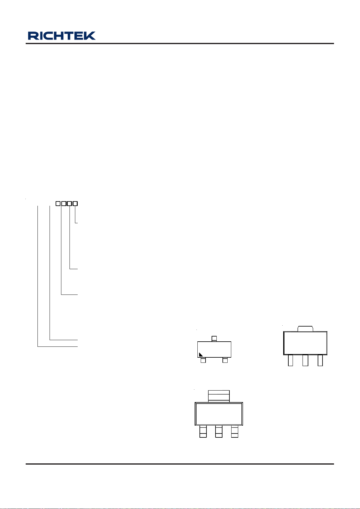
For ease of application, the RT9161/A comes in the popular
3-pin SOT-23 (300mA), SOT-89 (300mA), SOT-223
(500mA), or TO-92 packages.
Ordering Information
RT9161/A-
Package Type
V : SOT-23-3
X : SOT-89
G : SOT-223
ZL : TO-92 (L-Type)
ZT : TO-92 (T-Type)
Lead Plating System
P : Pb Free
G : Green (Halogen Free and Pb Free)
Output Voltage
15 : 1.5V
16 : 1.6V
:
49 : 4.9V
50 : 5.0V
500mA Output Current
300mA Output Current
Note :
Richtek products are :
` RoHS compliant and compatible with the current require-
ments of IPC/JEDEC J-STD-020.
` Suitable for use in SnPb or Pb-free soldering processes.
Features
zz
Low Dropout Voltage of 200mV at Output Current
z
zz
100mA, 450mV at Output Current 300mA, and
750mV at 500mA Output Current
zz
z Guaranteed 300/500mA Output Current
zz
zz
z Internal 1.5
zz
zz
z Low Ground Current 1 10
zz
zz
z 2% Accura cy Output V oltage
zz
zz
z Input Voltage Range up to 12V
zz
zz
z Extremely Tight Load Regulation
zz
zz
z Fast T ra nsient Respon se
zz
zz
z Current-limiting and Thermal-limiting
zz
zz
z RoHS Compliant and 100% Lead (Pb)-Free
zz
ΩΩ
Ω P-MOSFET Draws No Base Current
ΩΩ
μμ
μA
μμ
Applications
z Voltage Regulator for LAN Card, CD-ROM, and DVD
z Wireless Communication Systems
z Battery Powered Systems
Marking Information
For marking information, contact our sales representative
directly or through a Richtek distributor located in your
area.
Pin Configurations
(TOP VIEW)
VIN
3
123
VIN
GND
VOUT
(TAB)
SOT-89
GND
SOT-23-3
2
VOUT
2
1
GND
(TAB)
VIN
3
VOUT
SOT-223
DS9161/A-35 April 2011 www.richtek.com
1

RT9161/A
3
2
1VIN
TO-92 (L-Type)
Typical Application Circuit
V
IN
Functional Pin Description
Pin Name Pin Functio n
VOUT Output Voltage.
GND Ground.
C
1uF
VOUT
GND
3
2
1
VOUT
VIN
GND
TO-92 (T-Type)
+
IN
RT9161/A
VIN
GND
VOUT
+
C
OUT
10uF
Electrolytic
V
OUT
VIN Power Input.
Function Block Diagram
VIN
Current
Limiting
Sensor
Thermal
Shutdown
Error Amp
1.2V
Reference
VOUT
+
-
GND
DS9161/A-35 April 2011www.richtek.com
2
RT9161/A
Absolute Maximum Ratings
z Input Voltage ---------------------------------------------------------------------------------------------------------------- −0.3 to 14V
z Operating Junction Temperature Range ------------------------------------------------------------------------------- −40°C to 125°C
z Storage Temperature Range --------------------------------------------------------------------------------------------- −65°C to 150°C
z Power Dissipation, P
SOT-23-3--------------------------------------------------------------------------------------------------------------------- 0.4W
SOT-89 ----------------------------------------------------------------------------------------------------------------------- 0.571W
SOT-223 --------------------------------------------------------------------------------------------------------------------- 0.741W
TO-92 ------------------------------------------------------------------------------------------------------------------------- 0.625W
z Package Thermal Resistance (Note 1)
SOT-23-3, θJA--------------------------------------------------------------------------------------------------------------- 250°C/W
SOT-23-3, θJC--------------------------------------------------------------------------------------------------------------- 140°C/W
SOT-89, θJA----------------------------------------------------------------------------------------------------------------- 175°C/W
SOT-89, θJC----------------------------------------------------------------------------------------------------------------- 100°C/W
SOT-223, θJA---------------------------------------------------------------------------------------------------------------- 135°C/W
SOT-223, θJC--------------------------------------------------------------------------------------------------------------- 15°C/W
TO-92, θJA------------------------------------------------------------------------------------------------------------------- 160°C/W
TO-92, θJC------------------------------------------------------------------------------------------------------------------- 125°C/W
D
@ T
= 25°C
A
Electrical Characteristics
(TA = 25°C, CIN = 1μF, C
Parameter Symbol Test Conditions Min Typ Max Unit
Output Voltage Accuracy
Output Voltage Temperature
Coefficient
Line Regulation
Load Regulation (Note 2)
Current Limit
(Note 3)
Dropout Voltage (Note 4)
Standby Current
Note 1. θ
Note 2. Regulation is measured at constant junction temperature, using pulsed ON time.
Note 3. Current Limit is measured at constant junction temperature, using pulsed ON time.
Note 4. The dropout voltage is defined as V
is measured in the natural convection at TA = 25°C on a low effective single layer thermal conductivity test board of
JA
JEDEC 51-3 thermal measurement standard.
= 10μF, unless otherwise specified.)
OUT
ΔV
I
OUT
= 1mA, V
L
= 5V −2 -- 2 %
IN
-- 50 150
ΔV
IL = 1mA, VIN= 4.5 to 12V
LINE
ΔV
IL = 1m A to 300/500mA, VIN = 5V
LOAD
-- 2 3
-- 1 30/50 mV
RT9161 350 580 --
RT9161A
VIN = 5V, V
I
LIM
V
IL = 300/500mA
DROP
I
STANDBY IL
= 0, VIN = 12V
− V
IN
, which is measured when V
OUT
OUT
= 0V
500 900 --
-- 450/750 600/1000 mV
-- 110 180
is V
OUT
OUT(NORMAL)
− 100mV.
PPM/°C
%V
OUT
mA
μA
DS9161/A-35 April 2011 www.richtek.com
3
RT9161/A
>2 >
)
(
)
>2 >
)
(
)
Typical Operating Characteristics
Temperature Stability
3.4
V
= 3.3V
(°C)
OUT
V
OUT
OUT
125°C
= 2.5V
)
25°C
3.2
3
2.8
Output Voltage (V)
2.6
2.4
-50-250 255075100125
Temperature
Dropout Voltage (VIN-V
1
0.8
0.6
0.14
0.12
0.10
0.08
0.06
0.04
Quiescient Current (mA)
0.02
0.00
-30 0 30 60 90 120
Temperature
(°C)
Short Circuit Current
1.4
Quiescient Current vs. Temperature
1.2
1
0.8
125°C
25°C
VIN = 5V
0.4
Dropout Voltage (V)
0.2
V
= 3.3V
0
0 100 200 300 400 500
I
(mA)
Load
7
V
6
5
Input Voltage
Deviation
4
100
0
1
-100
Deviation (mV)
Output Voltage
-200
Line Transient Response
C
= 10μF Electrolytic
OUT
I
= 0.1A
OUT
T
≈
T
Time (100μS/Div
Time (100μs/Div)
OUT
V
OUT
= 25°C
T
A
= 3.3V
0.6
0.4
Short Circuit Current (A)
0.2
0
0246810
Input/Output Differential (V)
7
V
6
5
Input Voltage
Deviation
4
Line Transient Response
C
= 10μF Electrolytic
OUT
I
= 0.1A
OUT
T
V
OUT
T
= 25°C
A
= 2.5V
≈
T
Time (100μS/Div
Time (100μs/Div)
Output Voltage
Deviation (mV)
100
-100
-200
0
1
DS9161/A-35 April 2011www.richtek.com
4

RT9161/A
>
>
(
)
(
)
(
)
(
)
60
40
20
2
Deviation (mV)
Output Voltage
0
-20
≈
100
50
mA
1
1
Load Current
-50
60
40
20
Deviation (mV)
Output Voltage
0
2 >
Load Transient Response
CIN = 1μF
C
= 10μF
OUT
TA = 25°C
T
T
Time (100μs/Div)
Time (100μS/Div)
Load Transient Response
CIN = 1μF
= 10μF
C
OUT
TA = 25°C
T
VIN = 5V
V
= 3.3V
OUT
VIN = 5V
= 2.5V
V
OUT
≈
Output Voltage
Load Current
Output Voltage
Deviation (mV)
mA
Deviation (mV)
150
100
50
-50
200
100
10
-100
150
100
50
2 >
0
≈
1 >
2 >
0
Load Transient Response
CIN = 1μF
= 10μF
C
OUT
TA = 25°C
T
T
Time (100μS/Div)
Time (100μs/Div)
Load Transient Response
CIN = 1μF
= 10μF
C
OUT
TA = 25°C
T
VIN = 5V
V
= 3.3V
OUT
VIN = 5V
= 2.5V
V
OUT
≈
-20
≈
100
50
mA
1 >
1
Load Current
-50
T
Time (100μS/Div)
Time (100μs/Div)
PSRR
0
CIN = 1uF
C
= 10uF Tantalum
OUT
-10
V
= 5V
IN
V
= 3.3V
OUT
T
= 25°C
A
-20
-30
PSRR (dB)
-40
-50
-60
10 100 1000 10000 100000 1000000
Frequency (Hz)
100mA
10mA
-50
≈
≈
200
100
mA
1 >
10
Load Current
-100
T
Time (100μS/Div)
Time (100μs/Div)
≈
PSRR
0
CIN = 1uF
C
= 10uF Tantalum
OUT
-10
V
= 5V
IN
V
= 2.5V
OUT
T
= 25°C
A
-20
-30
PSRR (dB)
-40
-50
-60
1M100K10K1K
10 100 1000 10000 100000 1000000
Frequency (Hz)
100mA
10mA
1M100K10K1K
DS9161/A-35 April 2011 www.richtek.com
5

RT9161/A
Application Information
A 10uF capacitor with 200mΩ or higher ESR, connecting
between VOUT and GND pins, is recommended for
stability. A capacitor with ESR smaller than 200 mΩ may
cause VOUT oscillation as shown in Figure 1. Operating
temperature should be well considered to ensure that the
capacitance is no less than 10uF over the operating
temperature range. Please take the notice that Aluminum
electrolytic capacitors may cause VOUT oscillation when
operating below −25°C. The capacitance can be increased
without limit for better transient response.
A 1uF or higher capacitor should be placed between VIN
and GND to filter out input noise and ensure stable output
voltage.
Region of Stable C
100
V
= 3.3V
IN
C
= 1uF
IN
C
= 10uF
OUT
10
1
ESR (Ω)
OUT
C
0.1
ESR vs. Load Current
OUT
Stable
Instable
P
Where T
temperature 125°C, T
θ
= ( T
D(MAX)
J(MAX)
is the junction to ambient thermal resistance.
JA
− TA ) / θ
J(MAX)
JA
is the maximum operation junction
is the ambient temperature and the
A
For recommended operating conditions specification of
RT9161/A, where T
is the maximum junction
J(MAX)
temperature of the die (125°C) and TA is the maximum
ambient temperature. The junction to ambient thermal
resistance θJA is layout dependent. For SOT-223 packages,
the thermal resistance θJA is 135°C/W on the standard
JEDEC 51-3 single-layer 1S thermal test board. The
maximum power dissipation at TA = 25°C can be calculated
by following formula :
P
= ( 125°C − 25°C ) / 250 = 0.400 W for
D(MAX)
SOT-23-3 packages
P
= ( 125°C − 25°C ) / 175 = 0.571 W for
D(MAX)
SOT-89 packages
P
= ( 125°C − 25°C ) / 135 = 0.741 W for
D(MAX)
SOT-223 packages
P
= ( 125°C − 25°C ) / 160 = 0.625 W for
D(MAX)
TO-92 packages
0.01
0 100 200 300 400 500
Load Current (mA)
Figure 1
Thermal protection limits power dissipation in RT9161/A.
When the operation junction temperature exceeds 165°C,
the OTP circuit starts the thermal shutdown function and
turns the pass element off. The pass element turn on again
after the junction temperature cools by 30°C.
For continuous operation, do not exceed absolute
maximum operation junction temperature 125°C. The
power dissipation definition in device is :
PD = (V
IN
− V
OUT
) x I
+ VIN x I
OUT
Q
The maximum power dissipation depends on the thermal
resistance of IC package, PCB layout, the rate of
surroundings airflow and temperature difference between
junction to ambient. The maximum power dissipation can
be calculated by following formula :
The maximum power dissipation depends on operating
ambient temperature for fixed T
and thermal
J(MAX)
resistance θJA. For RT9161/A packages, the Figure 2 of
derating curves allows the designer to see the effect of
rising ambient temperature on the maximum power
allowed.
800
700
600
500
400
300
SOT-23-3 package
200
100
Maximum Power Dissipation (mW)
0
0 153045607590105120
SOT-223 package
TO-29 package
SOT-89 package
Ambient Temperature
(°C)
Figure 2. Derating Curves
DS9161/A-35 April 2011www.richtek.com
6

Outline Dimension
RT9161/A
D
E
L
b
e
D1
A1
A
C
Symbol
Dimensions In Millimeters Dimensions In Inches
Min Max Min Max
A 3.175 4.191
0.125 0.165
A1 1.143 1.372 0.045 0.054
b 0.406 0.533
C 0.406 0.533
0.016 0.021
0.016 0.021
D 4.445 5.207 0.175 0.205
D1 3.429 5.029
E 4.318 5.334
e 1.143 1.397
L
12.700
3-Lead TO-92 Plastic Package
0.135 0.198
0.170 0.210
0.045 0.055
0.500
DS9161/A-35 April 2011 www.richtek.com
7

RT9161/A
D
C
e
A
b
Dimensions In Millimeters Dimensions In Inches
Symbol
Min Max Min Max
A 0.889 1.295 0.035 0.051
A1 0.000 0.152 0.000 0.006
B
A1
H
L
B 1.397 1.803 0.055 0.071
b 0.356 0.508 0.014 0.020
C 2.591 2.997 0.102 0.118
D 2.692 3.099 0.106 0.122
e 1.803 2.007 0.071 0.079
H 0.080 0.254 0.003 0.010
L 0.300 0.610 0.012 0.024
SOT-23-3 Surface Mount Package
DS9161/A-35 April 2011www.richtek.com
8

D
D1
RT9161/A
A
C
b1
e
b
e
A
b
Dimensions In Millimeters Dimensions In Inches
Symbol
Min Max Min Max
A 1.397 1.600 0.055 0.063
b 0.356 0.483 0.014 0.019
B 2.388 2.591 0.094 0.102
b1 0.406 0.533 0.016 0.021
B
C1
H
C 3.937 4.242 0.155 0.167
C1 0.787 1.194 0.031 0.047
D 4.394 4.597 0.173 0.181
D1 1.397 1.753 0.055 0.069
e 1.448 1.549 0.057 0.061
H 0.356 0.432 0.014 0.017
3-Lead SOT-89 Surface Mount Package
DS9161/A-35 April 2011 www.richtek.com
9

RT9161/A
Symbol
Dimensions In Millimeters Dimensions In Inches
Min Max Min Max
A 1.400 1.800 0.055 0.071
A1 0.020 0.100
0.001
0.004
b 0.600 0.840 0.024 0.033
B 3.300 3.700 0.130 0.146
C 6.700 7.300 0.264 0.287
D 6.300 6.700 0.248 0.264
b1 2.900 3.100 0.114 0.122
e 2.300 0.091
H 0.230 0.350 0.009 0.014
L 1.500 2.000 0.059 0.079
L1 0.800 1.100 0.031 0.043
3-Lead SOT-223 Surface Mount Package
Richtek Technology Corporation
Headquarter
5F, No. 20, Taiyuen Street, Chupei City
Hsinchu, Taiwan, R.O.C.
Tel: (8863)5526789 Fax: (8863)5526611
Information that is provided by Richtek Technology Corporation is believed to be accurate and reliable. Richtek reserves the right to make any change in circuit
design, specification or other related things if necessary without notice at any time. No third party intellectual property infringement of the applications should be
guaranteed by users when integrating Richtek products into any application. No legal responsibility for any said applications is assumed by Richtek.
10
Richtek Technology Corporation
Taipei Office (Marketing)
5F, No. 95, Minchiuan Road, Hsintien City
Taipei County, Taiwan, R.O.C.
Tel: (8862)86672399 Fax: (8862)86672377
Email: marketing@richtek.com
DS9161/A-35 April 2011www.richtek.com

 Loading...