

Page 1

R-IN32M4-CL2
Board design editio n
Userʼs Manual
Renesas Electronics
User’s Manual:
All information contained in these materials, including pr oduct s and product specifications,
represents informat ion o n t he pr oduct at the time of publication and is subject to change by
Renesas Electronics Corp. without notice. Please review the latest information published by
Renesas Electronics Corp. through various means, including the Renesas Electronic s Corp.
website (http://www.renesas. com).
Document number: R18UZ0046EJ0200
Issue date: Dec. 28, 2018
www.renesas.com
Page 2

Notice
1. Descriptions of circuits, softw are and other related information in this document are provided only to illustrate the
operation of semiconductor products and application examples. You are fully responsible for the incorporation of these
circuits, software, and information in the design of your equipment. Renesas Electronics assumes no responsibility for
any losses incurred by you or third parties arising from the use of these circuits, software, or information.
2. Renesas Electronics has used reasonable care in preparing the information included in this document, but Renesa s
Electronics does not warrant that such information is error free. Renesas Electronics assumes no liabili ty w hatsoever
for any damages incurred by you resulting from errors in or omissions from the information included herein.
3. Renesas Electronics does not assume any liability for infringement of patents, copyrights, or other intellectual property
rights of third parties by or arising from the use of Renesas Electronics products or technical information described in
this document. No license, express, implied or otherwise, is granted hereby under any patents, copyrights or other
intellectual property rights of Renesas Electronics or others.
4. You should not alter, modify, copy, or otherwise misappropriate any Renesas Electronics product, whether in whole or
in part. Renesas Electronics assumes no responsibility for any losses incurred by you or third parties arising from such
alteration, modification, copy or otherwise misappropriation of Renesas Electronics product.
5. Renesas Electronics products are classified according to the following two quality grades: "Standard" and "High
Quality". The recommended applications for each Renesas Electronics product depends on the product's quality gra de,
as indicated below.
"Standard": Computers; office equipment; communications equipment; test and measurement equipment; audio
and visual equipment; home electronic appliances; machine tools; personal electronic equipment;
and industrial robots etc.
"High Quality": Transportation equipment (automobiles, trains, ships, etc.); traffic control systems; anti-disaster
systems; anti-crime systems; and safety equipment et c.
Renesas Electronics products are neither intended nor authorized for use in products or systems that may pose a
direct threat to human life or bodily injury (artificial life support devices or systems, surgical implantations etc.), or may
cause serious property damages (nuclear reactor control systems, military equipment etc.). You must check the quality
grade of each Renesas Electronics product before using it in a particular application. You may not use any Renesas
Electronics product for any application for which it is not intended. Renesas Electronics shall not be in any way liable
for any damages or losses incurred by you or third parties arising from the use of any Renesas Electronics product for
which the product is not intended by Renesas Electronics.
6. You should use the Renesas Electronics products described in this document within the range specified by Renesas
Electronics, especially with respect to the maximum rating, operating supply voltage range, movement power voltage
range, heat radiation characteristics, installation and other product characteristics. Renesas Electronics shall have no
liability for malfunctions or damages arising out of the use of Renesas Electronics products beyond such specified
ranges.
7. Although Renesas Electronics endeavors to improve the quality and reliability of its products, semiconductor products
have specific characteristics such as the occurrence of failure at a certain rate and malfunctions under certain use
conditions. Further, Renesas Electronics products are not subject to radiation resistance design. Please be sure to
implement safety measures to guard them against the possibility of physical injury, and injury or damage caused by fire
in the event of the failure of a Renesas Electronics product, such as safety design for hardware and software including
but not limited to redundancy, fire control and malfunction prevention, appropriate treatment for aging degradation or
any other appropriate measures. Becau se the ev aluat ion of micr oco mp uter softw ar e alone is very diffic ult, please
evaluate the safety of the final products or systems manufactured by you.
8. Please contact a Renesas Electronics sales office for details as to environmental matters such as the environmental
compatibility of each Renesas Electronics product. Please use Renesas Electronics products in compliance with all
applicable laws and regulations that regulate the inclusion or use of controlled substances, including without limitation,
the EU RoHS Directive. Renesas Electronics assumes no liability for damages or losses occurring as a result of your
noncompliance with applicable laws and regulations.
9. Renesas Electronics products and technology may not be used for or incorporated into any products or systems whose
manufacture, use, or sale is prohibited under any applicable domestic or foreign laws or regulations. You should not use
Renesas Electronics products or technology described in this document for any purpose relating to military applications
or use by the military, including but not limited to the development of weapons of mass destruction. When exporting the
Renesas Electronics products or technology described in this document, you should comply with the applicable export
control laws and regulations and follow the procedures required by such laws and regulations.
10. It is the responsibility of the buyer or distributor of Renesas Electronics products, who distributes, disposes of, or
otherwise places the product with a third party, to notify such third party in advance of the contents and conditions set
forth in this document, Renesas Electronics assumes no responsibility for any losses incurred by you or third parties as
a result of unauthorized use of Renesas Electronics products.
11. This document may not be reproduced or duplicated in any form, in whole or in part, without prior written consent of
Renesas Electronics.
12. Please contact a Renesas Electronics sales office if you have any questions regarding the information contained in this
document or Renesas Electronics products, or if you have any other inquiries.
(Note 1) "Renesas Electronics" as used in this document means Renesas Electronics Corporation and also includes its
majority-owned subsidiaries.
(Note 2) "Renesas Electronics product(s)" means any product developed or manufactured by or for Renesas Electronics.
Page 3

ensure that the reset line is only released after full stabilization of the clock signal. Moreover, when switching to a
- Arm® and Cortex® are registered trademarks of Arm Limited (or its subsidiaries) in the EU and/or elsewhere.
Instructions for the use of product
In this section, the precautions are described for over whole of CMOS device.
Please refer to this manual about individual precaution.
When there i s a mention unlike the text of this manual, a mention of the text takes first priority.
1. Handling of Unused Pins
Handle unused pins in accord with the directions given under Handling of Unused Pins in the manual.
- The input pins of CMOS products are generally in the high-impedance state. In operation with an unused pin in
the open-circuit state, extra electromagnetic noise is induced in the vicinity of LSI, associated shoot-through
current flows internally, and malfunctions occur due to the false recognition of the pin state as an input signal
become possible. Unused pins should be handled as described under Handling of Unused Pins in the manual.
2. Processing at Power-on
The state of the product is undefined at the moment when power is supplied.
- The states of internal circuits in the LSI are indeterminate and the states of register settings and pins are
undefined at the moment when power is supplied.
In a finished product where the reset signal is applied to the external reset pin, the states of pins are not
guaranteed from the moment when power is supplied until the reset process is completed.
In a similar way, the states of pins in a product that is reset by an on-chip power-on reset function are not
guaranteed from the moment when power is supplied until the power reaches the level at which resetting has
been specified.
3. Prohibition of Access to Reserved Addresses
Access to reserved addresses is prohibited.
- The reserved addresses are provided for the possible future expansion of functions. Do not access these
addresses; the correct operation of LSI is not guaranteed if they are accessed.
4. Clock Signals
After applying a reset, only release the reset line after the operating clock signal has become stable. When
switching the clock signal during program execution, wait until the target clock signal has stabilized.
- When the clock signal is generated with an external resonator (or from an external oscillator) during a reset,
clock signal produced with an external resonator (or by an external oscillator) while program execution is in
progress, wait until the target clock signal is stable.
All rights reserved.
- Ethernet is a registered trademark of Fuji Xerox Co., Ltd.
- IEEE is a registered trademark of the Institute of Electrical and Electronics Engineers Inc.
- CC-Link and CC-Link IE Field are registered trademarks of CC-Link Partner Association (CLPA).
- TRON is an acronym for "The Real-time Operation system N ucle us".
- ITRON is an acronym for "Industrial TRON".
- μITRON is an acronym for "Micro Industrial TRON".
- TRON, ITRON, and μITRON do not refer to any specific product or products.
- Additionally all product names and service names in this document are a trademark or a registered trademark which
belongs to the respective owners.
Page 4

within the body of the text, at the end of each section, and in the Usage Notes section.
point in this document.
refer to it.
Document Name
Document Number
R-IN32M4-CL2 User’s Manual
R18UZ0032EJ****
R-IN32M4-CL2 User’s Manual: Peripheral Modules
R18UZ0034EJ****
R-IN32M4-CL2 User’s Manual: Gigabit Ethernet PHY
R18UZ0044EJ****
R-IN32M4-CL2 Programming Manual: Driver
R18UZ0036EJ****
R-IN32M4-CL2 Programming Manual: OS
R18UZ0040EJ****
R-IN32M4-CL2 User’s Manual: Board des ign edi tion
This manual
How to Use This Manual
1. Purpose and Target Readers
This manual is intended for users who wish to understand the functions of an Ethernet communication LSI "R-IN32M4CL2" for designing app lic a tion of it. It is assumed that the reader of this manual has general knowledge in the fields of
electrical engineering, logic circuits, and microcontrollers.
Particular attention should be paid to the precautionary notes when using the manual. These notes occur
The revision history summarizes the locations of revisions and additions. It does not list all revisions. Refer to
the text of the manual for details.
The mark "<R>" means the updated point in this revision. The mark "<R>" let users search for the updated
Related
Documents
The related documents indicated in this publication may include preliminary versions. However,
preliminary versions a re not marked as such. Please be understand ing of this beforehand. In addition,
because we make document at development, planning of each core, the related document may be the
document for individual customers. Last four digits of document number (described as ****) indicate
version information of each document. Please download the latest document from our web site and
The document related to R-IN32M4-CL2
Page 5

2. Notation of Numbers and Symbols
Weight in data notation: Left is high-order column, right is low-order column
Active low notation:
xxxZ (capital letter Z after pin name or signal name)
or xxx_N (capital letter _N after pin name or signal name)
or xxnx (pin name or signal name contains small l etter n)
Note:
Explanatio n of (Note) i n the text
Caution:
Item deserving extra attention
Remark:
Supplementary explanation to the text
Numeric notation:
Binary … xxxx , xxxxB or n’bxxxx (n bits)
Decimal … xxxx
Hexadecimal … xxxxH or n’hxxxx (n bits)
Prefixes representing powers of 2 (address space, memory capacity):
K (kilo)… 2
M (mega)… 2
G (giga)… 2
Data Type:
Word … 32 bits
Halfword … 16 bits
Byte … 8 bits
10
= 1024
20
= 10242
30
= 10243
Page 6

Contents
1.
Overview ........................................................................................................................................................ 1
1.1 Definitio n of Pin Hand ling and Symbols in This Manual ................................................................................... 1
2. Power/Reset Pins .......................................................................................................................................... 2
2.1 Power-O n/O ff Se q ue nc e ..................................................................................................................................... 2
2.2 Power Supply Pins .............................................................................................................................................. 4
2.3 Reset Pins ........................................................................................................................................................... 5
3. Clock Input Pins ............................................................................................................................................. 6
3.1 Pin Functions ...................................................................................................................................................... 6
3.2 Notes on Configuring the Oscillation Circuit ..................................................................................................... 7
3.3 Configuration Example of Oscillation Circuits................................................................................................... 9
4. PLL Power Supply Pins ............................................................................................................................... 10
4.1 Recommended Configuration of Filter ............................................................................................................. 10
4.2 Notes on Placement of Peripheral Components ................................................................................................ 11
5. GPIO Port Pins ............................................................................................................................................ 12
6. Gigabit Ethernet PHY Pins .......................................................................................................................... 13
6.1 Power Supply Peripheral Circ uit ...................................................................................................................... 13
6.1.1 Circuit Configuration ............................................................................................................................... 13
6.1.2 Recommended Components .................................................................................................................... 14
6.2 Peripheral Circuit of Pulse Transformer ........................................................................................................... 15
6.2.1 Example of Circuit Configurat ion ........................................................................................................... 15
6.2.2 Recommended Components .................................................................................................................... 16
6.3 REF_REXT and REF_FILT Pins ..................................................................................................................... 17
6.3.1 Example of Circuit Configurat ion ........................................................................................................... 17
6.3.2 Recommended Resistors .......................................................................................................................... 17
6.3.3 Recommended Ceramic Capacitors ......................................................................................................... 17
6.4 PHYADD Pin Handling .................................................................................................................................... 18
6.4.1 Example of P in Handling ......................................................................................................................... 18
6.4.2 Handling of Pins ...................................................................................................................................... 18
6.5 Notes on Board Wiring ..................................................................................................................................... 19
Contents-1
Page 7

7. Thermal Design <R> ................................................................................................................................... 22
7.1 Deciding on whether Particular Measures for Heat Dissipation are Required .................................................. 22
7.1.1 Estimating Tj ........................................................................................................................................... 22
7.1.2 Estimating Power Consumption .............................................................................................................. 22
7.1.3 Thermal Resistances under the JEDEC Conditions (for θja and Ψjt) ...................................................... 23
7.1.4 Results of Estimating Po wer Consu mption of the 1-V Sub-Systems at Tj .............................................. 24
7.1.5 Relation between Temperature Increases (∆t) and Thermal Resistance (θja) at a Given Ambient
Temperature ............................................................................................................................................. 25
7.2 Examples of Measures for Heat Dissipation ..................................................................................................... 26
7.2.1 Measures for Heat Release in Designing the Board ................................................................................. 27
7.2.2 Heat Dissipation from the Periphery (Including the Casin g) ................................................................... 29
7.3 Caution <R> ..................................................................................................................................................... 30
7.3.1 Handling of Unused Pins ......................................................................................................................... 30
8. CC-Link Pins ................................................................................................................................................ 31
9. CC-Link IE Field Pins .................................................................................................................................. 33
9.1 Caution .............................................................................................................................................................. 33
10. External MCU/Memory Interface Pins ......................................................................................................... 34
10.1 External MCU Interface .................................................................................................................................... 35
10.1.1 Asynchronous-SRAM Supporting MCU Connection Mode ................................................................... 36
10.1.2 Synchronous-SRAM Supporting MCU Connection Mode ...................................................................... 38
10.1.3 Synchronous-Burst-Transfer Supporting MCU Connec tion Mode.......................................................... 40
10.2 External Memory Interface ............................................................................................................................... 44
10.2.1 Asynchronous SRAM MEMC ................................................................................................................. 44
10.2.2 Synchronous Burst Access MEM C ......................................................................................................... 47
11. Serial Flash ROM Connection Pins ............................................................................................................. 50
12. As ynchro nous Ser i al Int erfac e J Connec ti on Pins ...................................................................................... 51
13. I2C Connection Pins .................................................................................................................................... 52
14. CAN Pi ns ..................................................................................................................................................... 53
15. CSIH Pins <R> ............................................................................................................................................ 54
15.1 One Master and One Slave ............................................................................................................................... 54
15.2 One Master and Two Slaves ............................................................................................................................. 54
Contents-2
Page 8

16. A/D Converter Pins ...................................................................................................................................... 55
17. JTAG/Trace Pins ......................................................................................................................................... 56
18. Implementation Conditions .......................................................................................................................... 60
19. Package Information .................................................................................................................................... 61
20. Mount Pad Information ................................................................................................................................ 62
21. BSCAN Information ..................................................................................................................................... 63
21.1 BSCAN Operating Conditions .......................................................................................................................... 63
21.2 Maximum Operating Frequency of TCK .......................................................................................................... 63
21.3 IDCODE ........................................................................................................................................................... 63
21.4 BSCAN Non-Supported Pins ............................................................................................................................ 64
21.5 How to Get BSDL ............................................................................................................................................ 65
22. IBIS Information ........................................................................................................................................... 66
23. Marking Information ..................................................................................................................................... 67
24. Countermeasure for Noise <R> .................................................................................................................. 68
24.1 Stopping Cl ock Output ..................................................................................................................................... 68
Contents-3
Page 9

Description
Low level
This pin is connected to GND.
High level
This pin supplies VDD33 (3.3 V).
Frame GNDAnalog GND
GND
R18UZ0046EJ0200
R-IN32M4-CL2 User’s Manual: Board design edition Dec. 28, 2018
1. Overview
This manual is intended for being us ed by engi neers that work on a circuit and P C B design that is equipp ed with an
Ethernet communication LSI from the R-IN32M4-CL2 made by Renesas Electronics.
The target device is the R-IN32M4-CL2. It is recommended to stud y thi s manual carefully and to follow the
recommend ations duri ng the circ uit and board design.
1.1 Definition o f Pin Handling and Symbols in This Manual
Pin handling and symbols are defined as follows in this manual.
Table 1.1 Definition of Pin Handling
Figure 1.1 Definition of GND Symbols
R18UZ0046EJ0200 Page 1 of 68
Dec. 28, 2018
Page 10

External Power Supply
Voltage[V]
Power Supplied to
External Pin Name
R-IN32M4
VDD33, AVDD
GbE-PHY
VDD33_GPHY
VDD25
2.5±0.125
GbE-PHY
VDD25A
PLL_VDD
VDD1A
R-IN32M4-CL2 User’s Manual: Board design edition 2. Power/Reset Pins
2. Power/Reset Pins
2.1 Power-On/Off Sequence
Table 2.1 lists the external power supply to the R-IN32M4 and GbE-PHY. In addition, Figure 2.1 shows the power on/off
sequence. (GbE stands for Gigabit Ethernet.)
Though ther e is no spec ific order for supplying the power-supply voltages, we recommend supplying the VDD33
external power after supplying the VDD10 external power. Conversely, we recommend shutting down VDD10 after
VDD33.
If VDD33 is supplied first, the input/output modes of I/O buffer are unstable rather than fixed during the period from
VDD33 rising to VDD10 rising, and thus caution is required on this point.
Make sure to confirm that the power supply voltage is stable before applying 3.3 V to I/O pins.
Table 2.1 External Power Supply
VDD33 3.3±0.165
VDD10 1.0±0.05 R-IN32M4 VDD10
GbE-PHY VDD1
R18UZ0046EJ0200 Page 2 of 68
Dec. 28, 2018
Page 11

GND
90
% VDD33
90%
VDD33
10%
VDD10
10
% VDD10
95
%
VDD33
95
%
VDD25
95
%
VDD10
50 ms
100
ms
50
ms
VDD
33
VDD
25
VDD
10
100 ms
External power supply
R-
IN32M4
-CL2
R-IN32M4
GbE-PHY
2.
5±0.125V
VDD33
VDD10 VDD10
VDD33 VDD25
3.3±0.165V
1.0±0.05V
R-IN32M4-CL2 User’s Manual: Board design edition 2. Power/Reset Pins
(1) Power on
Supply power in a way that satisfies both conditions below.
1. The time from whichever is first to do so among VDD33, VDD25, and VDD10 reaches 10% VDD until all power
supplies exceed 90% VDD is within 100 ms.
2. The time from whichever is first to do so among VDD33, VDD25, and VDD10 reaches 95% VDD until all power
supplies exceed 95% VDD is within 50 ms.
(2) Power off
Supply power in a way that satisfies both conditions below.
1. The time from whichever is first to do so among VDD33, VDD25, and VDD10 reaches 90% until all power
supplies fall below 10% VDD is within 100 ms.
2. The time from whichever is first to do so among VDD33, VDD25, and VDD10 reaches 95% until all power
supplies fall below 95% VDD is within 50 ms.
Figure 2.1 Power-On/Off Sequence
Figure 2.2 Power Supply Channel to R-IN32M4 Chip and GbE-PHY
R18UZ0046EJ0200 Page 3 of 68
Dec. 28, 2018
Page 12

Pin Name
Function
Reference for Connection Example
PLL_VDD
PLL power supply (1.0 V)
See section 4, PLL Power Supply Pins.
PLL_GND
PLL_GND
See section 4, PLL Power Supply Pins.
regulator or DC-DC converter.
regulator or DC-DC converter.
GND
Ground potential for power supply (GND)
Connect GND of the system (board).
use the ferrite bead or the lik e.
use the ferrite bead or the lik e.
VDD33_GPHY
GbE-PHY internal power supply (3.3 V)
See Section 6.1, Power Supply Peripheral Circuit.
VDD25A
GbE-PHY analog power supply (2.5 V)
See Section 6.1, Power Supply Peripheral Circuit.
VDD1
GbE-PHY internal power supply (1.0 V)
See Section 6.1, Power Supply Peripheral Circuit.
VDD1A
GbE-PHY analog power supply (1.0 V)
See Section 6.1, Power Supply Peripheral Circuit.
R-IN32M4-CL2 User’s Manual: Board design edition 2. Power/Reset Pins
2.2 Power Supply Pins
This is a list of power supply pins of R-IN32M4-CL2. When designing with these pins, r efer to the connection example
as follows.
VDD33 R-IN32M4 I/O power supply (3.3 V) Supply power from the power unit such as a
VDD10 R-IN32M4 internal power supply (1.0 V) Supply power from the power unit such as a
AVDD Analog power supply for A/D converter
(3.3 V)
AGND Analog power supply for A/D converter
(GND)
Supply power from the power unit such as a
regulator or DC-DC converter.
To reduce the effect of noise, it is recommended to
Connect GND of the system (board).
To reduce the effect of noise, it is recommended to
R18UZ0046EJ0200 Page 4 of 68
Dec. 28, 2018
Page 13

Pin Name
Function
Reference for Connection Example
RESETZ
Reset input
-
Link IE field)
TRSTZ
JTAG reset signal
See Section 17, JTAG/Trace Pins.
RSTOUTZ
External reset output
-
R-IN32M4-CL2 User’s Manual: Board design edition 2. Power/Reset Pins
2.3 Reset Pins
This is a list of rese t pins of R-IN32M4-CL2.
As a width at low level of at least 1 µs is required for the reset input signals, secure this by applying the low level of the
reset signal over the oscillation stabilization time of the external oscillator (25 MHz).
In addition, de-assert the RESETZ and HOTRESETZ signals after de-asserting t he P ONRZ signal.
HOTRESETZ Hot reset input (reset pin for bypass mode of CC-
PONRZ Power-on reset input for built-in RAM
-
-
R18UZ0046EJ0200 Page 5 of 68
Dec. 28, 2018
Page 14

Pin Name
Attribute
Function
In external clock input mode (OSCTH = 1), drive XT1 to the low level.
input via XT2.
High level: XT2 is to be connected to an oscillator.
Note:
Connection with an oscillator is recommended.
R-IN32M4-CL2 User’s Manual: Board design edition 3. Clock Input Pins
3. Clock Input Pins
3.1 Pin Functions
This is a list of pin functions of clock input pins.
XT1 Input Connects an external oscillator .
XT2 I/O Connects an external oscillator .
When OSCTH = 0, this pin functions as an output pin.
In external clock input mode (OSCTH = 1), the clock signal from an external oscillator is
OSCTH
Note
Input Selects the clock oscillation source to be conne cted to the clock pin .
Low level: XT1 and XT2 are to be connected to a resonator.
R18UZ0046EJ0200 Page 6 of 68
Dec. 28, 2018
Page 15

R
-IN32M4-CL2
OSCTH
XT1 XT2
Board
GND pattern
R-IN32M4-CL2 User’s Manual: Board design edition 3. Clock Input Pins
3.2 Notes on Configuring the Oscillation Circuit
As the R-IN32M4-CL2 includes an oscillation block, oscillation circuits are easily configurable by externally connecting
a resonator and components for external constants. Though configuring an osci lla tion circuit is easy, the configured
circuit is analog and operates at a high frequency, so notes that differ for logic become applicable.
To achieve stable operation of the o scilla tion circuit, set components for external constants to the optimum values
(capacitors on the input and output sides, and limiting resistors) and observe the following points required for an analog
circuit.
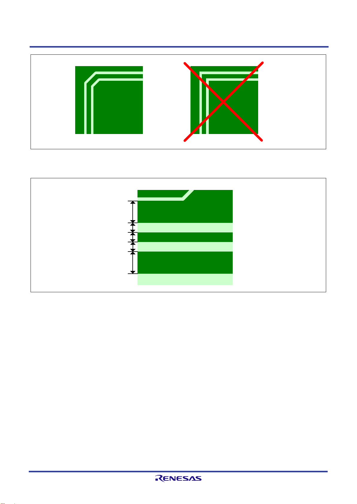
・Place the oscillation circuit near the R-IN32M4-CL2.
・Place the oscillation circuit as far as p ossible from high-frequency input pins such as clock pins.
・Place the resonators and components for external constants immediately clo se to the input and output pins of
oscillation circuit, and keep the connections as short as possible.
・Make the ground connections of the capacitors to the GND pins of R-IN32M4-CL2 as short and thick as possible.
・Make the lead wires between the resonator and capacitors as short as possible.
・Surround the components for external constant parts by as muc h GND wiring as is possible.
Figure 3.1 Example of GND Pattern for the Components for Ex ternal Constants
R18UZ0046EJ0200 Page 7 of 68
Dec. 28, 2018
Page 16

R-IN32M4-CL2 User’s Manual: Board design edition 3. Clock Input Pins
In addition, the following points to note should be observed in evaluating and determining the external constants.
・The range o f oscillating operati on may vary due to the dielectric constant of the board’s material, so use the actual
printed circuit board that will be used in the finished des ign.
・Check use of the board with the developed R-IN32M4-CL2 and the actual resonator to be mounted on it.
R18UZ0046EJ0200 Page 8 of 68
Dec. 28, 2018
Page 17

(1) Resonator input mode (2) External clock input mode
OSCTH
XT1
XT2
Resonator
C
1
C
2
Rd
OSCTH
XT1
XT2
Though Rd is an element to suppress the
excitation current and negative resistance of the
resonator, it may not be required depending on
the resonator to be used.
In external clock input mode, drive
XT1 to the low level.
R-IN32M4-CL2 R-IN32M4-CL2
VDD33 (3.3 V)
:
The input of
When
corresponding
Renesas
•
•
https://global.kyocera.com/prdct/electro/product/crystal-device/
R-IN32M4-CL2 User’s Manual: Board design edition 3. Clock Input Pins
3.3 Configuration Example of Oscillation Circuits
The following figure shows the configuration example of oscillation circu its.
Figure 3.2 Configuration Example of the Oscillation Circuit
Caution
a resonator is to be used, contact the resonator manufacturer and ask for a
Nihon Dempa Kogyo Co., Ltd. (NDK)
http://www.ndk.com/en/index.html
KYOCERA Crystal Device Corporation
the R-IN32M4-CL2 is fixed to 25 MHz.
part number and external constants.
recommends the following oscillator and resonator manufacturers.
R18UZ0046EJ0200 Page 9 of 68
Dec. 28, 2018
Page 18

C
1
PLL
PLL_GND
PLL_VDD
R
-
IN32
M
4-
CL2
VDD10 (1.0 V)
C
2
C1
: 0.
1-µ
F ceramic capacitor
C2: ≥ 4.7-µF capacitor
FB
FB
FB: Impedance
: 600
Ω at
100 MHz / DC resistance component
: 0.3
Ω or below
Reference ferrite beads
: TDK MPZ2012S601
A, MPZ
1608S601A
:
Place C1
If C2 is not placed immediately close to R-IN32M4-CL2, this will not cause any problems.
R-IN32M4-CL2 User’s Manual: Board design edition 4. PLL Power Supply Pins
4. PLL Power Supply Pins
The PLL circuit is susceptible to noise. To reduce the influence of noise, it is recommended to place filters in the power
supply pins of the PLL. In addition, to reduce the effects of noise between the power supplies for the board and PLL, the
use of ferrite beads is recommended.
4.1 Recommended Configuration of Filter
Figure 4.1 shows the rec ommended configurati on of the filter for the PLL po wer supply pins.
Figure 4.1 Recommended Configuration of Filter
Caution
immediately close to R-IN32M4-CL2.
R18UZ0046EJ0200 Page 10 of 68
Dec. 28, 2018
Page 19

PLL_
GND
PLL_
VDD
C1
Pay particular attention to the effects of
noise from signals with wiring running
parallel to these lines in this region.
C2
FB
GND
FB
Power supply
n:
PLL_VDD and P
Longer
more readily leading to effects.
R-IN32M4-CL2 User’s Manual: Board design edition 4. PLL Power Supply Pins
4.2 Notes on Placement of Peripheral Components
The 0.1-µF ceramic capacitor (C1) should be placed immediately close to R-IN32M4-CL2 (in the immediate vicinity of
the pin).
Figure 4.2 is a schematic view from below the board.
In addition, the wiring pattern s for the electrolytic capacitor (C2) and ferrite beads running parallel to other signal lines
should be avoided.
Figure 4.2 Schematic View from Below the Board
Cautio
wiring leads to stronger crosstalk because the LC components of the wiring increase,
LL_GND lines should be as short and thick as possible in PCB wiring.
R18UZ0046EJ0200 Page 11 of 68
Dec. 28, 2018
Page 20

R-IN32M4-CL2 User’s Manual: Board design edition 5. GPIO Port Pin s
5. GPIO Port Pins
GPIO is a general-purpose I/O port. As for the internal configur ation, see the section in the following document.
Section 7, Port Functions in the R-IN32M4-CL2 User’s Manual
R18UZ0046EJ0200 Page 12 of 68
Dec. 28, 2018
Page 21

10 µF
10 µF
10 µF
For the number
of pins
R-IN32M4-CL2 power
VDD1A
VDD1A
VDD1
VDD1
VDD1
VDD1
VDD25A
VDD25A
VDD25A
3.3 V
power plane
VDD33_GPHY
VDD33_GPHY
VDD33_GPHY
VDD33_GPHY
VDD33_GPHY
VDD33_GPHY
VDD33_GPHY
VDD33_GPHY
PLL_VDD
VDD10VDD33
GbE-PHY power
Place these
capacitors as close
to the respective
power source pins as
is possible.
Place these
capacitors as close
to the respective
power source pins
as is possible.
1.0 V
power plane
2.5 V
power plane
AVDD
◎ Decoupling capacitors (bypass capacitors)
Placing one within 0.5 inches of each power supply
pin is preferable.
Give priority to the placement of bypass capacitors
for GbE-PHY power pins. When placing bypass
capacitors for all of the R-IN power supply pins is
difficult, arrange one for every two or three pins.
47 µF 10 µF
10 µF
See Section 4, PLL
Power Supply Pins.
See Section 15, A/D
Converter Pins.
R-IN power
0.1 µF
Ferrite
bead
Ferrite
bead
47 µF 10 µF
R-IN32M4-CL2 User’s Manual: Board design edition 6. Gigabit Ethernet PHY Pins
6. Gigabit Ethernet PHY Pins
Since the Gigabit Ethernet PHY interface handles high-speed transfer, designing the board pattern for it and other
components requires full consideration on numerous points.
Design it in accord with the advice in this section.
6.1 Power Supply Peripheral Circuit
6.1.1 Circuit Configuration
Figure 6.1 Configuration of Gigabit Ethernet PH Y Power Supply Peripheral Circ uit
R18UZ0046EJ0200 Page 13 of 68
Dec. 28, 2018
Page 22

Manufacturer
Part Number
Capacitors
TDK
C32165R1C476M1160AB
47 µF
TDK
C2012X5R1C106K085AC
10 µF
TDK
C0603X5R0J104K030BC
0.1 µF
Manufacturer
Part Number
Impedance
Rated Current
Capacitors
muRata
BLM18PG121SN1
120Ω±25%
2 A
50mΩ
muRata
BLM21PG121SN1
120Ω±25%
3 A
30mΩ
R-IN32M4-CL2 User’s Manual: Board design edition 6. Gigabit Ethernet PHY Pins
6.1.2 Recommended Components
(1) Ceramic capacitors
We recommend using components that satisfy the following conditio ns.
Capacitors: 47 µF, 10 µF, and 0.1 µF
Thermal characteristic: X5R or X7R
ESR: No more than 0.1Ω (from 100 kHz to 100 MHz)
Table 6.1 Example of Recommended Components of Ceramic Capacitors
(2) Ferrite beads
We recommend using components that satisfy the following conditions.
Impedance: At least 80Ω (at 100 MHz)
Use beads with a high impedance in which the resistive component is dominant.
Rated current: At least 2 A
DC resistance: No more than 50mΩ
Figure 6.2 Example of Recommended Impedance Characteristics with Frequency of Ferrite Beads
Table 6.2 Example of Recommended Components of Ferrite Beads
R18UZ0046EJ0200 Page 14 of 68
Dec. 28, 2018
Page 23

Remark:
n = 0, 1
R-IN32M4-CL2 User’s Manual: Board design edition 6. Gigabit Ethernet PHY Pins
6.2 Peripheral Circuit o f Pulse Tr ans f or mer
An example of the circuit configuration for the Gigabit Ethernet PHY, pulse transformers, and RJ-45 connector, and
recommended pulse transformer products are shown below.
6.2.1 Example of Circuit Configuration
The circuits should be connected as shown in the following figure.
Figure 6.3 Peripheral Connection Example of Pulse Transformer
R18UZ0046EJ0200 Page 15 of 68
Dec. 28, 2018
Page 24

:
We
The impedance is 85, 100, or 115Ω
For details, contact the corresponding manufacturer.
Manufacturer
Product Type Name
Pulse
H5008NL
R-IN32M4-CL2 User’s Manual: Board design edition 6. Gigabit Ethernet PHY Pins
6.2.2 Recommended Components
We recommend using pulse transformer that satisfy the following conditions.
We also recommend the constitut i on illustrated in Transformer of Fig6.3.
Common-mode chokes are not required on the R-IN32M4-CL2 (PHY side) and is mounted on the connector.
Winding ratio: 1:1 (±2% or less, or ±3%) recommended
Return loss (see Figure 6.4): -18dB or le ss (1.0 MHz to 40 MHz)
-(12-20log(f/80))dB or less (40 MHz to 100MHz) *f: Frequency
Caution
recommend as little variation in return loss from 1.0 MHz to 40 MHz as possible.
.
Figure 6.4 Example of Return Loss of Pulse Transformer
Recommended components of the pulse transformer are as listed below.
R18UZ0046EJ0200 Page 16 of 68
Dec. 28, 2018
Page 25

1.0µF
2kΩ
REF_REXT
REF_FILT
Pla c e the wiring separately from that for other high-frequency
signals, but pl ac e the components close to the pins.
Join the wires
at a single
point, and
connect this to
GND.
Pla c e GND wiring as a guard.
R-IN32M4-CL2 User’s Manual: Board design edition 6. Gigabit Ethernet PHY Pins
6.3 REF_REXT and REF_FILT Pins
The method of handling the REF_REXT and REF_FILT pins and recommended values for the connected components
are shown below.
6.3.1 Example of Circuit Configuration
Figure 6.5 Example of Circuit Configuration for REF_REXT and REF_FILT
6.3.2 Recommended Resistors
We recommend using components that satisfy the following conditions.
Resistance value: 2kΩ, 1% accuracy
Rated power: At least 0.0625 W
6.3.3 Recommended Ceramic Capacitors
We recommend using components that satisfy the following conditions.
Capacitor: 1.0 µF, 10% accuracy
Thermal characteristic: C0G, X7R, or X5R
R18UZ0046EJ0200 Page 17 of 68
Dec. 28, 2018
Page 26

◎PHYADD[4:1] = 1111
PHYADD4
3.3 V
10 K
2.4 K
PHYADD3
3.3 V
10 K
2.4 K
PHYADD2
3.3 V
PHYADD1
3.3 V
PHYADD4
PHYADD3
PHYADD2
PHYADD1
◎PHYADD[4:1] = 0000
Floating
◎PHYADD[4:1] = 1010
PHYADD4
3.3 V
10 K
2.4 K
PHYADD3
PHYADD2
3.3 V
PHYADD1
Floating
Floating
Pin Name
Pin Handling
Low-level setting: Open circuit
Low-level setting: Open circuit
R-IN32M4-CL2 User’s Manual: Board design edition 6. Gigabit Ethernet PHY Pins
6.4 PHYADD Pin Handling
To change the PHY address, handle the pins as follows.
Leave the PHY address pins at 0000 (floating) unless otherwise specified.
6.4.1 Example of Pin Handling
6.4.2 Handling of Pins
The handling of pins depends on the pin. Handle the pins as fo llows.
PHYADD4, PHYADD3 High-le v el setting: Pulled u p to the 3.3-V power by a 2.4-kΩ resistor, and pulled down to
PHYADD2, PHYADD1 High-lev el setting: Connected to the 3.3-V power
GND by a 10-kΩ resistor
R18UZ0046EJ0200 Page 18 of 68
Dec. 28, 2018
Page 27

N
Pulse
transformer
R-
IN32M4-CL2
P
1 mm
Traces for the differential signal in the above
space should be of equal length.
Shorten the N trace.
R-IN32M4-CL2 User’s Manual: Board design edition 6. Gigabit Ethernet PHY Pins
6.5 Notes on Board Wiring
Pay attention to the foll owing no tes when placing the wiring on the board.
• Avoid long wir ing runs. We recommend to place the pulse transformer and the connector immediately as close as
possible to R-IN32M4-CL2.
• The components should be placed so that differential signal traces of TxP/N and RxP/N do not cross.
• Differentia l signal traces should be routed straight and as short as possible.
• Bends in lines sho uld be at angles of at least 135 degrees. (Figure 6.7)
• Differentia l signal traces between the R-IN32M4-CL2, pulse transformer, and RJ-45 connector should be designed
with a differential impedance of 100Ω ± 10% and with an impedance of 50Ω relating to GND.
• Diffe rential signal traces between the R-IN32M4-CL2 and pulse transformer, and those between the pulse
transformer and RJ-45 connector, should be equal in length. 0 .5 mm is the maximum deviation. Each of the
differential signal traces in e ach pair must be as nearly equal in length as is possible.
• As well as equal lengths, the designs o f signal lines for differential signals should be symmetrical. They should run
parallel to each other and be routed in the same layer. Placement of components, via holes, a nd the like should also
be symmetrical.
• Branches in signal lines act as stubs and should thus be avoided
• Place traces for differential signals with a separation from those for other signals. We recommend the width of the
gap to another signal line be at least five times the width of each differe ntial signal trace.
• Differential signal traces should not cross edges of the power/GND planes. The GND plane is desirable as the layer
below the differential signal trac e .
• Do not place any wiring, including any part of the power and GND planes, below the pulse transformer.
• Differential signal traces should be routed via as few via holes as possible. If via holes are essential, pay attention to
the following points.
- We recommend via holes for the related power and GND pla nes to be placed near the signal vias. The width
between the via holes for a signal and GND should be equal to the distance between the layers to avoid a
discontinuity in the impedance.
-
Metal planes close to the differential signal via holes could affect the impedance.
-
The diameter of a via hole should be almost equal to the width of the trace.
Figure 6.6 Example of Wiring for Dif f erenti al Sign als (1)
R18UZ0046EJ0200 Page 19 of 68
Dec. 28, 2018
Page 28
g
g
w
w
s
R-IN32M4-CL2 User’s Manual: Board design edition 6. Gigabit Ethernet PHY Pins
Figure 6.7 Example of Wiring for Diff erenti al Sign als (2)
Figure 6.8 Example of Wiring for Diff erenti al Sign als (3)
R18UZ0046EJ0200 Page 20 of 68
Dec. 28, 2018
Page 29

wa
w w
w
void
a
w
w
w
a
w
a
void
w
a
a
R-IN32M4-CL2 User’s Manual: Board design edition 6. Gigabit Ethernet PHY Pins
Figure 6.9 Example of Wiring for Diff erenti al Sign als (4)
R18UZ0046EJ0200 Page 21 of 68
Dec. 28, 2018
Page 30

Tj = Tt + Ψjt x power or Tj = Ta + θja x power
Tj
: Junction temperature [°C]
Tt
: Package surface temperature [°C]
Ta
: Ambient temperature [°C]
Thermal Resistances under the JEDEC Conditions (for θja and Ψjt).)
(
Thermal Resistances under the JEDEC Conditions (for θja and Ψjt).)
(1.0-V sub-systems + 2.5-V sub-systems + 3.3-V sub-systems)
Power (1.0-V sub-systems) = 320 + 100 × e
[mW]
R-IN32M4-CL2 User’s Manual: Board design edition 7. Thermal Design <R>
7. Thermal Design <R>
This section describes the thermal characteristics of the R-IN32M4-CL2, and includes notes that require attention in the
design of the board on which the device is mounted in terms of the dissipation of heat and the prevention of abnormal
heating. Since the R-IN32M4-CL2 incorporates a Gigabit Ethernet PH Y module and large-capacity memory, it requires
greater consideration of heat than most devices.
Design the board and casing in consideration of heat dissipation.
7.1 Deciding on whether Part ic ul ar Measur es for Heat Dissipation are Required
7.1.1 Estimating Tj
Take Tj ≤ 121.7°C as the criterion for Tj of the R-IN32M4-CL2. Estimate Tj from the following formul ae.
θja : Thermal resistance [°C/W] between the junction (at temperature Tj) and the ambient
environment (at Ta)
(See 0,
Ψjt : Thermal resistance [°C/W] between the junction (at temperature Tj) and the surface of
the package (at Tt)
See 0,
Power : Power consumption [W]
If Tj ≤ 121.7°C is satisf i ed, the semiconductor device does not require further measures for heat dissipation.
However, if the semiconductor device is to b e installed in ways that have var ying criteria for determining increases in
temperature, prepare measures for heat dissipation as required.
If Tj ≤ 121.7°C is not satisfied, heat dissipation solutions are necessary.
7.1.2 Estimating Power Consumption
For the 3.3-V and 2.5-V sub-systems, estimate the power consumption from the value for current on the R-IN32M4-CL2
user’s manual.
Since these are temperature dependent, the power consumption of the 1.0-V sub-systems is estimated from the following
formula according to the operating temperature.
(0.02106×Tj)
The list in 7.1.4, Results of Estimating Power Consumption of the 1-V Sub-Systems at Tj, gives results of estimation
under specific conditions.
R18UZ0046EJ0200 Page 22 of 68
Dec. 28, 2018
Page 31

θja [°C/W]
Ψjt [°C/W]
R-IN32M4-CL2
13.7
2.2
R-IN32M4-CL2 User’s Manual: Board design edition 7. Thermal Design <R>
7.1.3 Thermal Resistances under the JEDEC Conditions (for θja and Ψjt)
The thermal resistances under the JEDEC-2S2P conditions are as follows.
However, these values are for the devices alone; care is required since the actual thermal resistances will depend on the
board, casing, and peripheral components.
R18UZ0046EJ0200 Page 23 of 68
Dec. 28, 2018
Page 32

Tj [°C]
Power Consumption by 1-V Sub-Systems [mW]
(JEDEC)
(JEDEC)
-40
-20.2
-18.3
-10.8
-3.1
385.4
388.1
399.7
413.6
-35
-15.1
-13.2
-5.6
2.1
392.8
395.8
408.9
424.6
-30
-10.0
-8.0
-0.4
7.4
401.0
404.4
419.1
437.0
-25
-4.9
-2.9
4.8
12.8
410.3
414.1
430.7
450.9
-20
0.3
2.3
10.1
18.2
420.6
424.9
443.7
466.6
-15
5.4
7.5
15.4
23.6
432.2
437.0
458.2
484.5
-10
10.6
12.7
20.7
29.1
445.1
450.6
474.7
504.7
-5
15.8
17.9
26.1
34.7
459.6
465.8
493.2
527.7 0 21.0
23.1
31.5
40.4
475.8
482.8
514.1
554.0 5 26.3
28.4
37.0
46.1
494.0
502.0
537.8
584.1
10
31.6
33.8
42.5
52.0
514.5
523.6
564.8
618.9
15
36.9
39.1
48.1
58.0
537.5
548.0
595.5
659.2
20
42.2
44.5
53.8
64.2
563.5
575.5
630.7
706.3
25
47.6
50.0
59.6
70.6
592.8
606.7
671.1
761.9
30
53.1
55.5
65.6
77.2
626.0
642.1
717.8
828.5
35
58.6
61.1
71.7
84.3
663.7
682.4
772.2
909.7
40
64.2
66.8
77.9
91.8
706.6
728.6
836.2
1011.1
45
69.9
72.6
84.5
100.1
755.7
781.6
912.1
1143.1
50
75.7
78.6
91.3
109.7
812.0
842.9
1003.8
1328.0
N/A
N/A
N/A
N/A
N/A
N/A
N/A
N/A
N/A
N/A
N/A
N/A
N/A
N/A
N/A
N/A
N/A
N/A
N/A
N/A
N/A
N/A
N/A
N/A
R-IN32M4-CL2 User’s Manual: Board design edition 7. Thermal Design <R>
7.1.4 Results of Estimating Power Consumption of the 1-V Sub-Systems at Tj
The results of calculating power consumption by the 1-V sub-systems (maximum values) vary with the effects of θja and
Ta on Tj.
θja [°C/W]
Ta [°C]
13.7
15 20 25 13.7
15 20 25
55
60
65
70
75
80
85
81.5 84.6
87.6 90.9
93.8 97.4
100.2 104.2
106.9 111.4
114.0 119.2
121.7
98.5
106.4
115.3
876.9
952.4
1040.8
1145.3
1270.8
1424.2
1617.0
914.2 1116.7
997.9 1260.4
1097.2 1453.3
1216.7
1363.6
1549.7
R18UZ0046EJ0200 Page 24 of 68
Dec. 28, 2018
Page 33

Δt: Tt – Ta (
°C
)
Ta
: Ambient temperature (°C)
Tt: Package surface temperature (°C)
Tt
Ta
Δt
Note
Note.
The
casing.
R-IN32M4-CL2 User’s Manual: Board design edition 7. Thermal Design <R>
7.1.5 Relation between Temper ature Increases (∆t) and Thermal Resistance (θja) at a
Given Ambient Tempe r atur e
The thermal resistance (θja) of the R-IN32M4-CL2 depends on the board, casing, and peripheral components. If
respective criteria for the temperature rise (Δt = T
required θja to reach the target Δt. Take these values into consideration in the thermal design of the board.
As an example , the graph also shows the thermal resistance (actually measured) of the boards from Tessera Technology
Inc. and IA R Systems.
- Ta) apply to the end product, refer to the graph below that shows the
t
measured values and the result of simulation in the above figure were obtained without a
R18UZ0046EJ0200 Page 25 of 68
Dec. 28, 2018
Page 34

action.
dissipating gels should be applied, including for the casing as a whole if this is required.
.
I
surface layer and
layers as are possible.
.
Take
high temperatures.
R-IN32M4-CL2 User’s Manual: Board design edition 7. Thermal Design <R>
7.2 Examples of Measures for Heat Dissipation
We classify measures for heat dissipation into two types. For details, see the following pages.
(1) Measures for heat release in designing the board
• Take these types of measures into consideration when designing the board.
• The following measures are highly effective, so implement them as a matter of course.
(I) Thermal vias
(II) VDD/GND pattern
(III) Increase the number of board layers, and bring the GND pattern out to the surface layer.
(IV) Consider other factors of placement that will affect heat flows and take the appropriate
Note2
(2) Heat dissipation from the periphery (including the casing)
• If the measures listed in (1) above still don’t achieve your criterion for Δt or satisfy the condition Tj
= 121.7°C or below, further measures for heat dissipation in the form of heat sinks or heat
Notes 1
f increasing the number of layers in the board is difficult, bring the GND pattern out to the
make as many via connections between the GND patterns in different
Note1
2
special care in placement in terms of the regulator, since this operates at particularly
R18UZ0046EJ0200 Page 26 of 68
Dec. 28, 2018
Page 35

R-IN32M4-CL2 User’s Manual: Board design edition 7. Thermal Design <R>
7.2.1 Measures for Heat Release in Designing the Board
(1) Thermal Vias
Placing as many vias to the power supply and GND areas as possible below the center of the package increases the
number of paths for the flow of heat in the z direction. We recommend placing one via for each power supply and GND
ball.
(2) Power Supply and GND Planes
Secure as large an area as is possible for the power supply and GND planes of the board. This enables the broad diffusion
of heat through vias in the direct ion of the surface plane. Dividing paths for heat dissipation from plane to plane
decreases the effectiveness of heat dissipation. Therefore, place the GND pattern in such a way that the paths are divided
as little as is possible. We recommend L2 for the GND layer.
(3) Increase the Number of Board Layers, and Bring the GND Pattern out to the Surface Layer
Increasing the number of Cu wiring layers in the printed circuit board expands the area for hear release. Where possible,
place areas of the GND pattern on the surface layer and connect them to the main GND pattern via thermal vias. This
further improves heat dissipation. The board should have at least four layers, and we recommend six.
R18UZ0046EJ0200 Page 27 of 68
Dec. 28, 2018
Page 36

.
For example, placing a regulator with
has
the effect of significantly reducing its heat dissipation.
R-IN32M4-CL2 User’s Manual: Board design edition 7. Thermal Design <R>
(4) Appropriate Placement of Components
Placing heat-generating components close to this device affects its heat efficiency, so do not place heat-generating
components in its vicinity.
Caution
high power consumption in the vici nit y of this device
(5) Residual Copper Ratio of Cu Layers
Increasing the residual copper ratio in all layers of the board layers increases the breadth of the paths for heat transfer.
(6) Cu Thickness
Designing all Cu layers of the board to be thick increases the volume of paths for heat dissipation. Since thinner Cu
layers reduce the effectiveness of heat dissipation, care is required on this point. We recommend that the power supply
and GND layers be at least 35-um thick.
R18UZ0046EJ0200 Page 28 of 68
Dec. 28, 2018
Page 37

R-IN32M4-CL2 User’s Manual: Board design edition 7. Thermal Design <R>
7.2.2 Heat Dissipation from the Periphery (Including the Casing)
(1) Incorporating a Heat Sink
Incorporating a heat sink increases the area for heat dissipation, making heat dissipation fr o m the surface of the device
more efficient.
(2) Heat Conduction to the Casing
Placing heat dissipating gel on the surface of the device and connecting this to the metal surface of the casing increases
the efficie ncy of heat dissipatio n from the surface of the device.
(3) Placing a Fan in the Casing
Including a fan improves thermal conductivity through convection, which decreases the ambient temperature.
(4) Obtaining a Chimney Effect
Since heat tends to be released in the z direction, placing the board vertically leads to heat convection from the surface of
the device, improving the ther mal conductivity rate there.
(5) Enlarging Ventilation Holes
Larger ventilation holes accelerate the heat exchange between the air wit hin the casing and tha t outside, l owering the
temperature in the vicinity of the device.
(6) Thermal Insulation by Shielding Plates
If there is a particular source of much heat within the casing, thermal insulation by using shielding plates is effective.
Shielding t he device from the effects of such heat sources reduces the effect of the heat on the device.
R18UZ0046EJ0200 Page 29 of 68
Dec. 28, 2018
Page 38

R-IN32M4-CL2
Output mod e e nabled
Steady-state
current
R-IN32M4-CL2
Output mode disabled
Open-circuit
(floating)
Through-type
current
VDD33 (3.3 V)
VDD33 (3.3 V)
VDD33 (3.3 V)
VDD33 (3.3 V)
R-IN32M4-CL2 User’s Manual: Board design edition 7. Thermal Design <R>
7.3 Caution <R>
7.3.1 Handling of Unused Pins
If an unused pin is clamped to the GND or a power supply on the board, the corresponding pin must have the i nput
attribute as a fixed setting. If it is set as a n o utput, and the level at the point to which it is clamped is opposite that of the
pin, a large steady-state current will continuously flow through the output buffer.
On the other hand, if an unused pi n is open-circuit on the board, the corresponding pin can have either t he output attribute
or the input attribute as a fixed setting, ac c ompanied by enabling of the p ull-up or pull-down resistor. Setting a pin as an
input without enabling a pull-up or pull-down resistor may lead to the pin being in a floating state and the flow of a
through-type current.
Since the above factors lead to unnecessary heating, be sure to check the settings made by the software in these cases.
R18UZ0046EJ0200 Page 30 of 68
Dec. 28, 2018
Page 39

CC-Link Partner Association (CLPA)
TEL: 052-919-1588
FAX: 052-916-8655
Email: info@cc-link.org
Web: http://www.cc-link.org/jp/support/material/index.html
R-IN32M4-CL2 User’s Manual: Board design edition 8. CC-Link Pins
8. CC-Link Pins
A connection example for CC-Link remote device station is shown in Figure 8.1, Connection E xample for C C-Link
Remote Device Station.
For notes on the implementation of the CC-Link, refer to CC-Link Specifications: Implementation Specification (BAP-
05027) issued by the CC-Link Partner Association. Please contact the CC-Link Partner Association (CLPA) with any
requests for the corresponding material.
R18UZ0046EJ0200 Page 31 of 68
Dec. 28, 2018
Page 40

R-IN32M4-CL2
CCS_RD(P54)
CCS_SD(P56)
CCS_SDGA TE ON(P51)
2
3
5
4
SN75ALS181SN
13
14
5V
47k
47k
680
680
4
5
6
MC177050-A401
3
2
1
10
9
11
12
6
7
8
1
DA
DB
DC
SLD
FG
3300 pF
50V
HZU6.2ZTRF-E
CCS_STATION_NO_7(P77)
CCS_STATION_NO_6(P76)
CCS_STATION_NO_5(P75)
CCS_STATION_NO_4(P74)
CCS_STATION_NO_3(P73)
CCS_STATION_NO_2(P72)
CCS_STATION_NO_1(P71)
CCS_STATION_NO_0(P70)
8
4
2
1
8
4
2
1
CCS_BS_8(RP05)
CCS_BS_4(RP04)
CCS_BS_2(RP03)
CCS_BS_1(RP02)
8
4
2
1
STATION NO
X10
STATION NO
X1
B.RAT E
CCS_ERR Z(P25)
CCS_RUN Z(P26)
CCS_LNKRUNZ(P32)
CCS_RDZ (P54)
CCS_SDZ(P56)
VDD33(3.3V)
CCS_IOT ENSU (P22)
CCS_SENYU1(P24)
CCS_SENYU0(P23)
CCS_REF S TB (P50)
CCS_WDTZ(P12)
CCM_CLK80M
CCS_MON3(P12 or P67)
CCS_MON2(P01 or P11)
CCS_MON1(P00 or P10)
CCS_MON0(P06)
CCS_MON7(P05)
CCS_MON6(P04)
CCS_MON5(P03)
CCS_MON4(P55)
CCS_RES OUT(P07)
CCS_FUS EZ(P42)
8
4
2
1
123
4
876
5
330
RN-10k
LED
35605-5153-B00 PE
VCC
GND
Out put
OE
DSO32 1SR(80MHz)
33
0.1uF
4
2
3
1
RDEN L (Pxx)
Note
VDD33(3.3V)
VDD33(3.3V)
Note:
Control the RDENL signal by connecting it to a general-purpose output port pin.
R-IN32M4-CL2 User’s Manual: Board design edition 8. CC-Link Pins
Figure 8.1 Connection Example for CC-Link Remote Device Station
R18UZ0046EJ0200 Page 32 of 68
Dec. 28, 2018
Page 41

R-IN32M4-CL2 User’s Manual: Board design edition 9. CC-Link IE Field Pins
9. CC-Link IE Field Pins
9.1 Caution
When booting in external memory boot mode, external serial flash ROM boot mode, or instruction RAM boot mode,
drive the TRACEDATA2 pin (multiplexed with CCI_WAITEDGEH) and the TRACEDATA3 pin (multiplexed with
CCI_WRLENH ) high during a reset.
If the TRACEDATA2 and TRACEDATA3 pins are driven low during a reset, accessing the CC-Link IE field from the
CPU in the R -IN32M4-CL2 is not possible.
R18UZ0046EJ0200 Page 33 of 68
Dec. 28, 2018
Page 42

Mode Setting
External Connection Mode
MEMIFSEL
MEMCSEL
HIFSYNC
ADMUXMODE
Asynchronous SRAM MEMC
Synchronous burst access MEMC
Asynchronous-SRAM supporting MCU connection mode
Synchronous-SRAM supporting MCU connection mode
-
Setting prohibited
-
Setting prohibited
(address/data separated)
(address/data multiplexed)
ote:
Before
connection mode (MEMIFSEL high, MEMCSEL low, HIFSYNC high).
R-IN32M4-CL2 User’s Manual: Board design edition 10. External MCU/Memory Interface Pins
10. External MCU/Memory Interface Pins
This LSI is able to connect an external MCU or memory .
The connection mode is decided by the signal level of the MEMIFSEL, MEMCSEL, HIFSYNC, and ADMUXMODE
pins as shown in Table 10.1
Table 10.1 Mode Selection of External MCU/Memory Connection
Low Low - - External memory interface
High - - External memory interface
High Low Low - External MCU interface
High - External MCU interface
Note
High Low
High Low External MCU interface
Synchronous-burst-transfer su ppor ti ng MCU connection
mode
High External MCU interface
Synchronous-burst-transfer su ppor ti ng MCU connection
mode
N
access to the CC-Link IE field, select the synchronous-SRAM supporting MCU
R18UZ0046EJ0200 Page 34 of 68
Dec. 28, 2018
Page 43

aution:
The
MCU
Check the specifications of the product to be co nnected before determining the method.
R-IN32M4-CL2 User’s Manual: Board design edition 10. External MCU/Memory Interface Pins
10.1 External MCU Interface
The external MCU interface is multiplexed with the external memory interface. When the MEMIFSEL pin is set to the
high level, it functions as the external MCU interface.
The external MCU interface supports the asynchrono us-SRAM supporting MCU connection mode and the sync hronousSRAM supporting MCU connection mode. When the level on the HIFSYNC pin is high, it functions as a synchronous
SRAM inter face, and when HIFSYNC is set to low-level, it functions a s an asynchronous SRAM interface (see Table
10.1, Mode Selection of External MCU/Memory Connection).
In addition, the external MCU interface supports the synchronous-burst-transfer supporting MCU connection mode of
clock sync hronization, allowing access to large volumes of data at high speed. This function is enabled by setting the
MEMIFSEL and MEMCSEL pins to the high level.
C
method of connection for each signal depends on the bus interface specifications of the
to be connected.
R18UZ0046EJ0200 Page 35 of 68
Dec. 28, 2018
Page 44

R-IN32M4-CL2
External MCU
A2-A20
D0-D31
CSZ
HPGCSZ
Note3
HA2-HA20
Note4
HD0-HD31
PGCSZ
RDZ
HCSZ
HRDZ
WAITZHWAITZ
WRSTBZHWRSTBZ
Interrupt, port pin
HERROUTZ
Note2
HWRZ0 / HBENZ0
Note1
(WRZ0) / BENZ0
(WRZ1) / BENZ1
(WRZ2) / BENZ2
(WRZ3) / BENZ3
HWRZ1 / HBENZ1
Note1
HWRZ2 / HBENZ2
Note1
HWRZ3 / HBENZ3
Note1
HBUSCLK
R-
IN32M4-CL2
External MCU
A1-A20
D0-D15
CSZ
HPGCSZ
Note3
HA1-HA20
Note5
HD0-HD15
PGCSZ
RDZ
HCSZ
HRDZ
WAITZ
HWAITZ
WRSTBZHWRSTBZ
Interrupt, port pin
HERROUTZ
Note2
HBUSCLK
HWRZ0 / HBENZ0
Note1
(WRZ0) / BENZ0
(WRZ1) / BENZ1HWRZ1 / HBENZ1
Note1
R-IN32M4-CL2 User’s Manual: Board design edition 10. External MCU/Memory Interface Pins
10.1.1 Asynchronous-SRAM Supporti ng MCU Connection Mode
The following figure shows a general connection example in asynchronous-SRAM supporting MCU i nterface mode,
when thi s LSI chip is connected as a slave device to an external MCU.
Figure 10.1 Connection Example of 32-Bit External MCU Interface (in Asynchronous-SRAM Supporting
MCU Connection Mode)
Figure 10.2 Connection Example of 16-Bit External MCU Interface (in Asynchronous-SRAM Supporting
R18UZ0046EJ0200 Page 36 of 68
Dec. 28, 2018
MCU Connection Mode)
Page 45

1.
selected by the level on the HWRZSEL pin.
2.
Connect it to an interrupt or general-purpose port input of the MCU to be connected, if required.
3.
4.
IN32M4-CL2.
5.
IN32M4-CL2.
R-IN32M4-CL2 User’s Manual: Board design edition 10. External MCU/Memory Interface Pins
Notes
HWRZ0-HWRZ3 and HBENZ0-HBENZ3 are multiplexed on the same pins, and the pin functions are
Connecting the HERROUTZ signal is not indispensable.
This is a chip-select signal supporting paged access. Connect it if required.
Connected the address signal for a 4-byte boundary from the destination to the HA2 pin of the R-
Connected the address signal for a 2-byte boundary from the destination to the HA1 pin of the R-
R18UZ0046EJ0200 Page 37 of 68
Dec. 28, 2018
Page 46
R-IN32M4-CL2
External MCU
A2-A20
D0-D31
CSZ
HPGCSZ
Note3
HA2-HA20
Note4
HD0-HD31
PGCSZ
RDZ
HCSZ
HRDZ
WAITZHWAITZ
WRSTBZHWRSTBZ
Interrupt, port pin HERROUTZ
Note2
HWRZ0 / HBENZ0
Note1
(WRZ0) / BENZ0
(WRZ1) / BENZ1
(WRZ2) / BENZ2
(WRZ3) / BENZ3
HWRZ1 / HBENZ1
Note1
HWRZ2 / HBENZ2
Note1
HWRZ3 / HBENZ3
Note1
HBUSCLK BUSCLK
R
-IN32M4-CL2
External MCU
A1-A20
D0-D15
CSZ
HPGCSZ
Note3
HA1-HA20
Note5
HD0-HD15
PGCSZ
RDZ
HCSZ
HRDZ
WAITZHWAITZ
WRSTBZHWRSTBZ
Interrupt, port pinHERROUTZ
Note2
HWRZ0 / HBENZ0
Note1
(WRZ0) / BENZ0
(WRZ1) / BENZ1
HWRZ1 / HBENZ1
Niote1
HBUSCLK BUSCLK
R-IN32M4-CL2 User’s Manual: Board design edition 10. External MCU/Memory Interface Pins
10.1.2 Synchronous-SRAM Suppor ti ng MCU Connection Mode
The following figure shows a general connection example in synchronous-SRAM supporting MCU interface mode, when
this LSI chip is connected as a slave device to an external MCU.
Figure 10.3 Connection Example of 32-Bit External MCU Interface (in Synchronous-SRAM Supporting MCU
Connection Mode)
Figure 10.4 Connection Example of 16-Bit External MCU Interface ( in Synchronous-SRAM Supporting MCU
Connection Mode)
R18UZ0046EJ0200 Page 38 of 68
Dec. 28, 2018
Page 47

.
HWRZ0
selected by the level on the HWRZSEL pin.
2.
Connecting the
Connect it to an interrupt or general-purpose port input of the MCU to be connected, if required.
3.
This is a chip-select signal supporting paged access. Connect it if required.
4.
Connected the address signal for a 4
IN32M4-CL2.
5.
Connected the address signal for a 2
IN32M4-CL2.
R-IN32M4-CL2 User’s Manual: Board design edition 10. External MCU/Memory Interface Pins
Notes 1
-HWRZ3 and HBENZ0-HBENZ3 are multiplexed on the same pins, and the pin functions are
HERROUTZ signal is not indispensable.
-byte boundary from the destination to the HA2 pin of the R-
-byte boundary from the destination to the HA1 pin of the R-
R18UZ0046EJ0200 Page 39 of 68
Dec. 28, 2018
Page 48

R-IN32
M4-CL2
External MCU
D
0-
D
31
CSZ
HBCYSTZ
HD
0
-H
D31
BCYSTZ
/ ADV
RDZ
HCSZ
HRDZ
WAITZHWAITZ
WRSTBZHWRSTBZ
Interrupt
, port pinHERROUTZ
Note2
HBUSCLK
H
WRZ0 / HBENZ0 BENZ0
BENZ1
BENZ2
BENZ3
HWRZ
1
/
HBENZ
1
HWRZ2
/ H
BENZ2
HWRZ
3 / HBENZ3
BUSCLK
HWRZSEL
Note
1
ADMUXMODE
HPGCSZ
PGCSZ
VDD33 (
3.3V)
R-IN32M4-CL2
External MCU
D0-D15
CSZ
HBCYSTZ
HD0-HD15
BCYSTZ / ADV
RDZ
HCSZ
HRDZ
WAITZ
HWAITZ
WRSTBZ
HWRSTBZ
Interrupt, port pin HERROUTZ
Note2
HWRZ0 / HBENZ0
BENZ0
BENZ1
HWRZ1 / HBENZ1
HBUSCLK BUSCLK
A17-A20
Note4
HA17-HA20
Note3
HWRZSEL
Note1
ADMUXMODE
HPGCSZ
PGCSZ
VDD33 (3.3V)
R-IN32M4-CL2 User’s Manual: Board design edition 10. External MCU/Memory Interface Pins
10.1.3 Synchronous-Burst-Transfer Supporting MCU Connection Mode
The following figure shows a general connection example in synchronous-burst-transfer supporting MCU connection
mode, when this LSI chip is connected as a slave device to an external MCU.
10.1.3.1 Address/Data Multiplexed Mode (ADMUXMODE = H)
Figure 10.5 Connection Example of 32-Bit External MCU Interface
Figure 10.6 Connection Example of 16-Bit External MCU Interface
R18UZ0046EJ0200 Page 40 of 68
Dec. 28, 2018
Page 49

Notes 1.
In this mode, drive the HWRZSEL pin low.
2.
Connect it to an interrupt or general-purpose port input of the MCU to be connected, if required.
3.
R-IN32M4-CL2.
4.
Accessed is by byte-wise addressing.
R-IN32M4-CL2 User’s Manual: Board design edition 10. External MCU/Memory Interface Pins
Connecting the HERROUTZ signal is not indispensable.
Connected the address signal for a 128-Kbyte boundary from the destination to the HA17 pin of the
R18UZ0046EJ0200 Page 41 of 68
Dec. 28, 2018
Page 50

R-IN32M4-CL2
External MCU
D0-D31
CSZ
HBCYSTZ
HD0-HD31
BCYSTZ / ADV
RDZ
HCSZ
HRDZ
WAITZ
HWAITZ
WRSTBZHWRSTBZ
Interrupt, port pin
HERROUTZ
Note2
HBUSCLK
HWRZ0 / HBENZ0 BENZ0
BENZ1
BENZ2
BENZ3
HWRZ1 / HBENZ1
HWRZ2 / HBENZ2
HWRZ3 / HBENZ3
BUSCLK
HWRZSEL
Note1
ADMUXMODE
A2-A20
Note4
HA1-HA19
Note3
HPGCSZ
PGCSZ
R
-
IN32
M4-CL2 External MCU
D0-D15
PGCSZ
HBCYSTZ
HD0-HD15
BCYSTZ /
ADV
RDZ
HPGCSZ
HRDZ
WAITZHWAITZ
WRSTBZHWRSTBZ
Interrupt,
port pin
HERROUTZ
Note2
HWRZ0 / HBENZ0 BENZ0
BENZ1HWRZ1 / HBENZ1
HBUSCLK
BUSCLK
A1-A20
Note4
HA1-HA20
Note3
HWRZSEL
Note1
ADMUXMODE
HCSZ CSZ
R-IN32M4-CL2 User’s Manual: Board design edition 10. External MCU/Memory Interface Pins
10.1.3.2 Address/Data Sep ar ated Mode (ADMUXMODE = L)
Figure 10.7 Connection Example of 32-Bit External MCU Interface
Figure 10.8 Connection Example of 16-Bit External MCU Interface
R18UZ0046EJ0200 Page 42 of 68
Dec. 28, 2018
Page 51

Notes 1.
In this mode, drive the HWRZSEL pin low.
2.
Connect it to an interrupt or general-purpose port input of the MCU to be connected, if required.
3.
16-bit width: Connected the address signal for a 16-bit boundary from the destination to the HA1 pin.
4.
Accessed is by byte-wise addressing.
R-IN32M4-CL2 User’s Manual: Board design edition 10. External MCU/Memory Interface Pins
Connecting the HERROUTZ signal is not indispensable.
32-bit width: Connected the address signal for a 32-bit boundary from the destination to the HA1 pin.
R18UZ0046EJ0200 Page 43 of 68
Dec. 28, 2018
Page 52

R-IN32M4-CL2 User’s Manual: Board design edition 10. External MCU/Memory Interface Pins
10.2 External Memory Interface
This section describes the connection as a master device to an external memory.
The operating connection mode of the external memory interface depends on the level of the signal on the MEMCSEL
pin (see Table 10.1, Mode Selection of External M C U / M emo ry Connection).
10.2.1 Asynchronous SRAM MEMC
The asynchr onous SRAM MEMC is externally connectable to paged ROM, ROM, SRAM, or peripheral devices with an
interface similar to the SRAM interface via a 16- or 32-bit bus.
The external MCU interfaces for the asynchrono us SRAM MEM C and the sync hro no u s method burst access MEMC are
multiplexed with each other. When both the MEMCSEL and MEMIFSEL pins are at the low level, t he asynchronous
SRAM MEMC can be used.
When both t he BOOT0 and BOOT1 pins are at the low level, booting up proceeds from the memory connected to CSZ0.
R18UZ0046EJ0200 Page 44 of 68
Dec. 28, 2018
Page 53

R-IN32M4-CL2
RDZ
A2-A19
D16-D31
CSZn
SRAM
(256 Kwords × 16 bits)
A0-A17
I/O1-I/O16
/CS
/UB
/WE
/OE
/LB
(WRZ3) / BENZ3
(WRZ2) / BENZ2
(WRZ1) / BENZ1
WRSTBZ
D0-D15
(WRZ0) / BENZ0
SRAM
(256 Kwords × 16 bits)
A0-A17
I/O1-I/O16
/CS
/UB
/WE
/OE
/LB
R-IN32M4-CL2
SRAM
(256 Kwords × 16 bits)
A0-A17
I/O1-I/O16
/CS
/UB
/WE
RDZ
A1-A18
/OE
/LB
CSZn
(WRZ1) / BENZ1
WRSTBZ
D0-D15
(WRZ0) / BENZ0
Remark:
n = 0 to 3
R-IN32M4-CL2 User’s Manual: Board design edition 10. External MCU/Memory Interface Pins
10.2.1.1 Connection Ex ample w i th SRAM
The following figure shows an example when this LSI chip is connected to SRAM.
Figure 10.9 Connection Example with 32-Bit SRAM (Asynchronous SRAM MEMC)
Figure 10.10 Connection Example with 16-Bit SRAM (Asynchronous SRAM MEMC)
R18UZ0046EJ0200 Page 45 of 68
Dec. 28, 2018
Page 54

R-IN32M4-CL2
RDZ
A2-A21
D16
-
D31
CSZ0
D0-D15
Paged ROM
(1 Mword × 16 bits)
A0-A19
O0-O15
/CE
/OE
WRSTBZ
/WE
Paged
ROM
(1 Mword × 16 bits)
A0-A19
O
0-
O
15
/CE
/OE
/WE
R-IN32M4-CL2
Paged ROM
(1Mword×16bit)
A0-A19
O0-O15
/CE
RDZ
A1-A20
/OE
CSZ0
D0-D15
/WEWRSTBZ
Caution:
The on-page mode of paged ROM can only be used when CSZ0 is connected.
R-IN32M4-CL2 User’s Manual: Board design edition 10. External MCU/Memory Interface Pins
10.2.1.2 Connection Example with Paged ROM
The following figure shows an example when this LSI chip is connected to paged ROM.
Figure 10.11 Connection Example with 32-Bit Paged ROM (Asynchronous SR AM ME MC)
Figure 10.12 Connection Example with 16-Bit Paged ROM (Asynchronous SRAM MEMC)
R18UZ0046EJ0200 Page 46 of 68
Dec. 28, 2018
Page 55

R-IN32M4-CL2 User’s Manual: Board design edition 10. External MCU/Memory Interface Pins
10.2.2 Synchronous Burst Access MEMC
The synchronous burst access MEMC is externally connectable to paged ROM, ROM, SRAM, PSRAM, NOR-flash
memory, or peripheral devices with an interface similar to the SRAM interface via a 16- or 32-bit bus.
In addition, setting the ADMUXMODE pin to the high level enables multiplexing of the address and data signals.
The external MCU interfaces for the synchronous me thod burst access MEMC and the asynchronous SRAM MEMC are
multiplexed with each other. When the ME MCSEL and MEMI FSEL pins are set to high level and low level respectively,
the synchronous burst access MEMC can be used.
When both t he BOOT0 and BOOT1 pins are at the low level, booting up proceeds from the memory connected to CSZ0.
R18UZ0046EJ0200 Page 47 of 68
Dec. 28, 2018
Page 56

R-IN32M4-CL2
SRAM
(256 Kwords × 16 bits)
A0-A17
Note
I/O1-I/O16
/CS
/UB
/WE
RDZ
A2-A19
Note
D16-D31
/OE
/LB
CSZn
(WRZ3) / BENZ3
(WRZ2) / BENZ2
(WRZ1) / BENZ1
WRSTBZ
D0-D15
(WRZ0) / BENZ0
BUSCLK BUSCLK
SRAM
(256 Kwords × 16 bits)
A0-A17
Note
I/O1-I/O16
/CS
/UB
/WE
/OE
/LB
BUSCLK
R-IN32M4-CL2
SRAM
(256 Kwords × 16 bits)
A0-A17
Note
I/O1-I/O16
/CS
/UB
/WE
RDZ
A1-A18
Note
/OE
/LB
CSZn
(WRZ1) / BENZ1
WRSTBZ
D0-D15
(WRZ0) / BENZ0
BUSCLK BUSCLK
Remark:
n = 0 to 3
Note:
When the address/data multiplex
level), separate connection of the addres s bus is not require d.
R-IN32M4-CL2 User’s Manual: Board design edition 10. External MCU/Memory Interface Pins
10.2.2.1 Connection Example with SRAM
The following figure shows an example when this LSI chip is connected to SRAM.
Figure 10.13 Connection Example with 32-Bit SRAM (Synchronous Burst Access MEMC)
Figure 10.14 Connection Example with 16-Bit SRAM (Synchronous Burst Access MEMC)
R18UZ0046EJ0200 Page 48 of 68
Dec. 28, 2018
ing feature is enabled (the ADMUXMODE pin is at the high
Page 57

R-IN32M4-CL2
Paged ROM
(1 Mword × 16 bits)
A0-A19
Note
O0-O15
/CE
RDZ
A2-A21
Note
D16-D31
/OE
CSZ0
D0-D15
/WEWRSTBZ
BUSCLK
BUSCLK
Paged ROM
(1 Mword × 16 bits)
A0-A19
Note
O0-O15
/CE
/OE
/WE
BUSCLK
R-IN32M4-CL2
Paged ROM
(1 Mword × 16 bits
)
A0-A19
Note
O0-
O15
/CE
RDZ
A1-A20
Note
/OE
CSZ0
D0-D15
/
WEWRSTBZ
BUSCLK
BUSCLK
Caution:
The on-page mode of paged ROM can only be used when CSZ0 is connected.
Note:
When the address/data multiplex
level), separate connection of the addres s bus is not require d.
R-IN32M4-CL2 User’s Manual: Board design edition 10. External MCU/Memory Interface Pins
10.2.2.2 Connection Example with Paged ROM
The following figure shows an example when this LSI chip is connected to paged ROM.
Figure 10.15 Connection Example with 32-Bit Paged ROM (Synchronous Burst Access MEMC)
Figure 10.16 Connection Example with 16-Bit Paged ROM (Synchronous Burst Access MEMC)
ing feature is enabled (the ADMUXMODE pin is at the high
R18UZ0046EJ0200 Page 49 of 68
Dec. 28, 2018
Page 58

R-IN32M4-CL2
Serial flash
memory
C (CLK)
D (IO0)
SMSCK (P14)
SMCSZ (P17)
/S (/CS)
SMIO0 (P15)
SMIO1 (P16)
SMIO2 (P10)
SMIO3 (P11)
Q (IO1)
/WP (IO2)
/
HOLD (IO3)
R-IN32M4-CL2 User’s Manual: Board design edition 11. Serial Flash ROM Connection Pins
11. Serial Flash ROM Connection Pins
This LSI chip has a memory controller to connect the serial flash ROM that supports the SPI compatible interface.
Figure 11.1 Connection Example with Serial Flash ROM
R18UZ0046EJ0200 Page 50 of 68
Dec. 28, 2018
Page 59

R
-IN32M4-CL2
RXD0 (P20)
TXD0 (P21)
TXD1 (P31)
RXD1 (P30)
UART device
Rxd
Txd
UART device
Rxd
Txd
R-IN32M4-CL2 User’s Manual: Board design edition 12. Asynchronous Serial Interface J Connect ion Pins
12. Asynchronous Serial Interface J Connection Pins
The following figure shows a conne ction example between the R-IN32M4-CL2 and the asynchronous serial interface J
(UARTJ) device.
Figure 12.1 Connection Example between R-IN32M4-CL2 and UART Device
R18UZ0046EJ0200 Page 51 of 68
Dec. 28, 2018
Page 60

R-IN32M4-CL2
Clock output
VDD33 (3.3 V)
SCLn
(Clock input
)
Data output
Data input
(
Clock output)
Slave device
Clock input
Data output
Data input
SCLn
SDAn SDAn
RP
00
(
SCL
1
)/
P
60
(
SCL
0)
RP
01(
SDA
1)/
P
61(
SDA0
)
VDD33 (3.3 V)
Remark:
n = 0 to 3
R-IN32M4-CL2 User’s Manual: Board design edition 13. I2C Connection Pins
13. I2C Connection Pins
Figure 13.1 Connection Example between R-IN32M4-CL2 and I2C Slave Device shows a connection example between
the R-IN32M4-CL2 and t he I
Since the serial clock line and serial data line are N-ch. open drain outputs, an external pull-up resistor is required.
2
C slave device.
Figure 13.1 Connection Example between R-IN32M4-CL2 and I2C Slave Dev ice
R18UZ0046EJ0200 Page 52 of 68
Dec. 28, 2018
Page 61

R-IN32M4-CL2
CAN transceiver
Rxd
Txd
CRXD0 (P53) /CRXD1 (P55)
CTXD0 (P54) /CTXD1 (P56)
CAN_H
CAN_L
CAN bus
R-IN32M4-CL2 User’s Manual: Board design edition 14. CAN Pins
14. CAN Pins
The following figure shows a conne ction example between the R-IN32M4-CL2 and the CAN transceiver.
The CAN transceiver is used to connect the CAN bus.
Figure 14.1 Connection Example between R-IN32M4-CL2 and CAN Transceiver
R18UZ0046EJ0200 Page 53 of 68
Dec. 28, 2018
Page 62

R
-IN32M4-CL2 (Master)
Slave
CSISCKn (out)
CSISOn
CSISIn
SCK (in)
MOSI
MISO
R-IN32M4-CL2 (Slave) Master
CSISCKn (in)
CSISIn
CSISOn
SCK (out)
MOSI
MISO
Remark
:
n = 0, 1
R-IN32M4-CL2 (Master) Slave 1
CSISCKn (out)
CSISOn
CSISIn
SCK (in)
MOSI
MISO
SSI
Slave 2
SCK (in)
MOSI
MISO
SSI
CSICSn0
CSICSn1
Remark:
n = 0, 1
R-IN32M4-CL2 User’s Manual: Board design edition 15. CSIH Pins <R>
15. CSIH Pins <R>
Examples of connections of the R-IN32M4-CL2 with a CSI master and slave are given below.
15.1 One Master and One Slav e
The following figure illustrates the connections between one master and one slave.
Figure 15.1 Direct Master/Slave Connection
15.2 One Master and Two Slav es
The following figure illustrate s the connections between an R-IN32M4-CL2 as a master and two slaves.
In this example, the R-IN32M4-CL2 supplies one chip select (CS) signal to each of the slaves. This signal is connected to
the slave select input (SSI) of the slave.
Figure 15.2 Connection between One Master and Two Slaves
R18UZ0046EJ0200 Page 54 of 68
Dec. 28, 2018
Page 63

10µF
R-IN32M4-CL2
AVREFP
AVREFM
AGND
AVDD
AIN0-AIN7
10µF
0.1µF
0.1µF
Note2
100
Ω
1000pF to
0.1µ
F
Analog input
Configuration example of low-pass filter circuit
ADTRG
(RP
02)
ADTRGRDY (
RP
03)
Place the
0.1-µF capacitor in the
immediate vicinity of the pin.
Since noise from the power supplies for
the digital systems affects the
3.
3V
/
AGND power-supply lines for the A/D
converter, we recommend using ferrite
beads and the like to separate the power
supply lines.
Control these signals according to the usage.
FB
FB
FB
FB
3
.
3V
Note1
3.3V
Note1
Note2
Note2
Notes 1.
Same potential as AVDD
2.
Same potential as AGND
R-IN32M4-CL2 User’s Manual: Board design edition 16. A/D Converter Pins
16. A/D Converter Pins
The following figure shows a recommended connection example between the A/D converter power supply pins and
analog input pins.
Figure 16.1 Recommended Connection Example for A/D Converter
R18UZ0046EJ0200 Page 55 of 68
Dec. 28, 2018
Page 64

About 4.7 kΩ to
10 kΩ
R-IN32M4-CL2
TCK
ICE connecter (20-pin half-pitch)
TCK
TMS
TDI
TDO
TMS
TDI
TDO
TRSTZ
nRESET
RESETZ
HOTRESETZ
Reset
circuit
VDD33 (3.3 V)
Wired OR connection with open drain
JTAGSEL
Not connected
R-IN32M4-CL2 User’s Manual: Board design edition 17. JTAG/Trace Pins
17. JTAG/Trace Pins
The following figures show examples when this LSI chip is connected to the ICE (in-circuit emulator).
They are examples when connected to the 20-pin half-pitch c onne cter or 20-p in full-pitch connecter of standard.
Figure 17.1 Connection Example of JTAG Interface (20-Pin Half-Pitch without Trace)
As long as nRESET is input to RESETZ, nRESET is not required to input to HOTRESETZ.
RESRTZ resets the entire LSI, but the internal PLL is not reset in the case of only HOTRESETZ. Please use it to meet
your needs. In addition, nRESE T should not be connect to PONRZ.
R18UZ0046EJ0200 Page 56 of 68
Dec. 28, 2018
Page 65

R-IN32M4-CL2
TCK
ICE connecter (20-pin half-pitch)
TCK
TMS
TDI
TDO
TMS
TDI
TDO
TRSTZ
nRESET
RESETZ
HOTRESETZ
Reset circuit
VDD33 (3.3 V)
About 4.7 kΩ to
10 kΩ
TRACECLK
TRACEDATA0
TRACEDATA1
TRACEDATA2
TRACECLK
TRACEDATA0
TRACEDATA1
TRACEDATA2
TRACEDATA3 TRACEDATA3
JTAGSEL
About 22 to 33 Ω
The wiring runs should preferably be no
longer than 50 mm. If the wiring runs have to
be longer than this because of the
circumstances of the set as a whole, they
should be kept within 100 mm.
Wired OR connection with open drain
Not connected
R-IN32M4-CL2 User’s Manual: Board design edition 17. JTAG/Trace Pins
Figure 17.2 Connection Example of JTAG Interface (20-Pin Half-Pitch with Trace)
R18UZ0046EJ0200 Page 57 of 68
Dec. 28, 2018
Page 66

R
-
IN32
M
4
-
CL2
TCK (SWCLK)
ICE connecter (20-pin half-pitch)
TCK (SWCLK)
TMS (SWDIO)
TDI
TDO
TMS (SWDIO)
TDI
TDO
TRSTZ
nRESET
RESETZ
HOTRESETZ
Reset
circuit
VDD33 (3.3 V)
About 4.7 kΩ to
10 kΩ
JTAGSEL
Wired OR connection with open drain
Not connected
Not connected
Not connected
R-IN32M4-CL2 User’s Manual: Board design edition 17. JTAG/Trace Pins
Figure 17.3 Connection Example of SWD Interface (20-Pin Half-Pitch without Trace)
R18UZ0046EJ0200 Page 58 of 68
Dec. 28, 2018
Page 67

R
-IN32M4-CL2
TCK
ICE connecter (20-pin full-pitch)
TCK
TMS
TDI
TDO
TMS
TDI
TDO
TRSTZ
nSRST
RESETZ
HOTRESETZ
Reset
circuit
About 4.7 kΩ to
10 kΩ
JTAGSEL
nTRST
Wired OR connection with open drain
VDD33 (3.3 V)
R-IN32M4-CL2 User’s Manual: Board design edition 17. JTAG/Trace Pins
Figure 17.4 Connection Example of JTAG Interface (20-Pin Full-Pitch)
R18UZ0046EJ0200 Page 59 of 68
Dec. 28, 2018
Page 68

Open the aluminum dry pack
Infrared reflow
(within 3 times)
Baking
(125°C, 24 to 72h)
Storage period is
within 7 days*
Yes
No
*Storage conditions: 5 to 30°C temperature,
less than 70% humidity
・Maximum temperature (package surface temperature)
: 250°C or below
・Time of maximum temperatur e
: 30 s or less
・Time over which the temperature is 217°C or more
: Within 150 s
・Time to reach preheating temperature (150 to 200°C)
: 60 to 120 s
・Maximum number of times to reflow
: 3 times
・
pack
: Within 7 days
Package surface temperature (°C)
Time (s)
60 to 120 s
(preheating)
150
°C
200
°C
217
°C
250
°C max.
60 to 150 s
30 s max.
245
°C
R-IN32M4-CL2 User’s Manual: Board design edition 18. Implementation Conditions
18. Implementation Conditions
The following figure s show implementation conditions of the R-IN32M4-CL2.
Figure 18.1 Implementation Flow
Safe-keeping restriction period after opening the dray
Figure 18.2 Infrared Reflow Temperature Profile
R18UZ0046EJ0200 Page 60 of 68
Dec. 28, 2018
Page 69

R-IN32M4-CL2 User’s Manual: Board design edition 19. Package Information
19. Package Information
The following figure shows the package information of R-IN32M4-CL2.
Figure 19.1 Package Information
R18UZ0046EJ0200 Page 61 of 68
Dec. 28, 2018
Page 70

1
.
00
mm
0.43 to 0.53 mm
0.50 to 0.70 mm
1.00 mm
0.43 to 0.53 mm
R-IN32M4-CL2 User’s Manual: Board design edition 20. Mount Pad Information
20. Mount Pad Information
The following figure shows the mount pad information of the R-IN32M4-CL2.
Figure 20.1 Mount Pad Sizes
R18UZ0046EJ0200 Page 62 of 68
Dec. 28, 2018
Page 71

:
If
the
Placing the 3st pin in the Hi-Z state creates a possibility of a floating current flowing.
IDCODE 0x082C7447
<breakdown>
Fixed code
1
R-IN32M4-CL2 User’s Manual: Board design edition 21. BSCAN Information
21. BSCAN Information
The R-IN32M4-CL2 provides the BSDL file.
Caution
the other device is connected to an input pin without the pin bei ng pulled up or down, clamp
level on the board or set the logic in the other device.
21.1 BSCAN Operating Conditions
Fix the leve l of the pins as follows.
• JTAGSEL: Fixed to the high level
• TMODE0: Fixed to the low level
• TMODE1: Fixed to the low level
• TMODE2: Fixed to the low level
21.2 Maximum Operating Frequency of TCK
The maximum operating frequency of TCK is 10 MHz.
21.3 IDCODE
IDCODE is as follows.
Version
Part number
Manufacturer number : Renesas Electronics
0000
1000 0010 1100 0111
0100 0100 011
R18UZ0046EJ0200 Page 63 of 68
Dec. 28, 2018
Page 72

R-IN32M4-CL2
TEST4, TEST5, and analog pins
R-IN32M4-CL2 User’s Manual: Board design edition 21. BSCAN Information
21.4 BSCAN Non-Supported Pins
The following pins do not support BSCAN.
Table 21.1 List of BSCAN Non-Supported Pins
XT1, XT2, PONRZ, JTAGSEL, TMODE0-TMODE2, T MS , TDI, TDO, TRSTZ, TCK, TMC1, TMC2, TE S T1 , TEST3,
R18UZ0046EJ0200 Page 64 of 68
Dec. 28, 2018
Page 73

R-IN32M4-CL2 User’s Manual: Board design edition 21. BSCAN Information
21.5 How to Get BSDL
With regard to obtain the BSDL file, please contact a Renesas Sales Representative or Distributor in your area.
R18UZ0046EJ0200 Page 65 of 68
Dec. 28, 2018
Page 74

R-IN32M4-CL2 User’s Manual: Board design edition 22. IBIS Information
22. IBIS Information
For IBIS information, please contact a Renesas Sales Representative or Distributor in your area.
R18UZ0046EJ0200 Page 66 of 68
Dec. 28, 2018
Page 75

R-IN32M4-CL2 User’s Manual: Board design edition 23. Marking Information
23. Marking Information
Product name: R9J03G019GBG
Figure 23.1 R-IN32M4-CL2 Marking Information
R18UZ0046EJ0200 Page 67 of 68
Dec. 28, 2018
Page 76

R-IN32M4-CL2 User’s Manual: Board design edition 24. Countermeasure for Noise <R>
24. Countermeasure for Noise <R>
This section describes a countermeasure for noise in circuits that include an R-IN32M4-CL2.
24.1 Stopping Clock Output
If the BUSCLK pin is not in use, output on the pin from the R-IN32M4-CL2 can be stopped. See section 2.2.2, Clock
Control Registers (CLKGTD0 , CLK G TD1) in the R-IN32M4-CL2 User’s Manual: Peripheral Modules regarding control
of the GCBCLK bit in the CLKGTD 1 register, which enables or disables output from the BUSCLK pin.
R18UZ0046EJ0200 Page 68 of 68
Dec. 28, 2018
Page 77

REVISION HISTORY
R-IN32M4-CL2 User’s M anual: Board design edition
Description
Page
Summary
0.01
Mar. 4, 2016
-
First edition issued
1.00
Feb. 28, 2017
1
1.1 Definition of Pin Handling and Symbols in This Manual, newly added
Note on OSCTH added
Representation of pin handling and GND in figure 3.2 modified
Representation of pin handling and GND in figure 4.1 modified
Representation of GND in figure 6.1 modified
Remark added
List of recommended components of the pulse transformer added
Description when the PHY address is not specif ied add ed
Representation of GND in the figure modified
Description added to precautionary notes
Description of measures for heat dissipation modified
Reference to a connection example for CC-Link remote device station added
31
Representation of pin handling and GND in figure 8.1 modified
Representation of pin handling in figures 10.1 and 10.2 modified
Representation of pin handling in figures 10.5 and 10.6 modified
Representation of pin handling in figures 10.7 and 10.8 modified
slave device added. Represent atio n of pin handlin g in figur e 13.1 mod ifie d
Representation of pin handling in figure 15.1 modified and notes added
Representation of pin handling in figure 16.1 modified
Representation of pin handling in figure 16.2 modified
R-IN32M4-CL2 User’s Manual: Board design edition REVISION HISTO RY
Rev. Date
6 3.1 Pin Functions
9 3.3 Configuration Example of Oscillation Circuits
10 4.1 Recommended Configuration of Filter
13 6.1.1 Circuit Configuration
15 6.2.1 Example of Circuit Configuration
Pin names and representation of GND in figure 6.3 modified
16 6.2.2 Recommended Components
18 6.4 PHYADD Pin Handling
18 6.4.1 Example of Pin Handling
19 6.5 Notes on Board Wiring
22 to 29 7. Guide to Thermal Design
30 8. CC-Link Pins
35 10.1.1 Asynchronous-SRAM Supporting MCU Connection Mode
39 10.1.3.1 Address/Data Multiplexed Mode (ADMUXMODE = H)
41 10.1.3.2 Address/Data Separated Mode (ADMUXMODE = L)
51 13. I2C Connection Pins
Reference to a connection example between the R-IN32M4-CL2 and the I2C
53 15. A/D Converter Pins
54 16. JTAG/Trace Pins
55 16. JTAG/Trace Pins
C-1
Page 78

Description
Page
Summary
Representation of pin handling in figure 16.3 modified
Representation of pin handling in figure 16.4 modified
Section title, modified
Newly added
Newly added
Newly added
—
Error corrected, description modified, and contents and expressions adjusted
R-IN32M4-CL2 User’s Manual: Board design edition REVISION HISTO RY
Rev. Date
1.00 Feb. 28, 2017 56 16. JTAG/Trace Pins
57 16. JTAG/Trace Pins
2.00 Dec. 28, 2018 22 7. Thermal Design
30 7.3 Caution
54 15. CSIH Pins
68 24. Countermeasure for Noise
C-2
Page 79

R-IN32M4-CL2 User’s Manual: Board design edition REVISION HISTO RY
[MEMO]
C-3
Page 80

Published by: Renesas Electronics Corporation
R-IN32M4-CL2 User’s Manual: Board design edition
Publication Date: Rev.0.01 Mar. 4, 2016
Rev.2.00 Dec. 28, 2018
Page 81

R-IN32M4-CL2 User’s Manual
Board design edition
R18UZ0046EJ0200
Page 82

http://www.renesas.com
Refer to "http://www.renesas.com/" for the latest and detailed information.
Renesas Electronics America Inc.
1001 Murphy Ranch Road, Milpitas, CA 95035, U.S.A.
Tel: +1-408-432-8888, Fax: +1-408-434-5351
Renesas Electronics Canada Limited
9251 Yonge Street, Suite 8309 Richmond Hill, Ontario Canada L4C 9T3
Tel: +1-905-237-2004
Renesas Electronics Europe Limited
Dukes Meadow, Millboard Road, Bourne End, Buckinghamshire, SL8 5FH, U.K
Tel: +44-1628-651-700, Fax: +44-1628-651-804
Renesas Electronics Europe GmbH
Arcadiastrasse 10, 40472 Düsseldorf, Germany
Tel: +49-211-6503-0, Fax: +49-211-6503-1327
Renesas Electronics (China) Co., Ltd.
Room 1709 Quantum Plaza, No.27 ZhichunLu, Haidian District, Beijing, 100191 P. R. China
Tel: +86-10-8235-1155, Fax: +86-10-8235-7679
Renesas Electronics (Shanghai) Co., Ltd.
Unit 301, Tower A, Central Towers, 555 Langao Road, Putuo District, Shanghai, 200333 P. R. China
Tel: +86-21-2226-0888, Fax: +86-21-2226-0999
Renesas Electronics Hong Kong Limited
Unit 1601-1611, 16/F., Tower 2, Grand Century Place, 193 Prince Edward Road West, Mongkok, Kowloon, Hong Kong
Tel: +852-2265-6688, Fax: +852 2886-9022
Renesas Electronics Taiwan Co., Ltd.
13F, No. 363, Fu Shing North Road, Taipei 10543, Taiwan
Tel: +886-2-8175-9600, Fax: +886 2-8175-9670
Renesas Electronics Singapore Pte. Ltd.
80 Bendemeer Road, Unit #06-02 Hyflux Innovation Centre, Singapore 339949
Tel: +65-6213-0200, Fax: +65-6213-0300
Renesas Electronics Malaysia Sdn.Bhd.
Unit 1207, Block B, Menara Amcorp, Amcorp Trade Centre, No. 18, Jln Persiaran Barat, 46050 Petaling Jaya, Selangor Darul Ehsan, Malaysia
Tel: +60-3-7955-9390, Fax: +60-3-7955-9510
Renesas Electronics India Pvt. Ltd.
No.777C, 100 Feet Road, HAL 2nd Stage, Indiranagar, Bangalore 560 038, India
Tel: +91-80-67208700, Fax: +91-80-67208777
Renesas Electronics Korea Co., Ltd.
17F, KAMCO Yangjae Tower, 262, Gangnam-daero, Gangnam-gu, Seoul, 06265 Korea
Tel: +82-2-558-3737, Fax: +82-2-558-5338
SALES OFFICES
© 2018 Renesas Electronics Corporation. All rights reserved.
Colophon 5.0
 Loading...