Renesas R2J20656ANP Schematics

Preliminary Datasheet
R2J20656ANP
R07DS0201EJ0100
Rev.1.00
Integrated Driver - MOS FET (DrMOS)
Jan 25, 2011
Description
The R2J20656ANP multi-chip module incorporates a high-side MOS FET, low-side MOS FET, and MOS-FET driver
in a single QFN package. The on and off timing of the power MOS FET is optimized by the built-in driver, making this
device suitable for large-current buck converters. The chip also incorporates a high-side bootstrap switch, eliminating
the need for an external SBD for this purpose.
Features
Compliant with Intel 6 6 DrMOS Specification.
Built-in power MOS FET suitable for Notebook, Desktop, Server application.
Low-side MOS FET with built-in SBD for lower loss and reduced ringing.
Built-in driver circuit which matches the power MOS FET
Built-in tri-state input function which can support a number of PWM controllers
High-frequency operation (above 1 MHz) possible
VIN operating-voltage range: 27 Vmax
Large average output current (Max. 3 5 A)
Achieve low power dissipation
Controllable driver: Remote on/off
Zero current detection for a diode emulation operation
Double thermal protection: Thermal Warning & Thermal Shutdown
Built-in bootstrapping Switch
Small package: QFN40 (6 mm 6 mm 0.95 mm)
Pb-free/Halogen-Free
Outline
THWN
DISBL#
ZCD_EN#
PWM
Integrated Driver-MOS FET (DrMOS)
QFN40 package 6 mm × 6 mm
VINGHBOOTVCIN
MOS FET Driver
CGND VDRV GL PGND
VSWH
110
40
Driver
Pad
Low-side MOS Pad
31
30 21
(Bottom view)
High-side
MOS Pad
11
20
R07DS0201EJ0100 Rev.1.00 Page 1 of 15
Jan 25, 2011
R2J20656ANP Preliminary
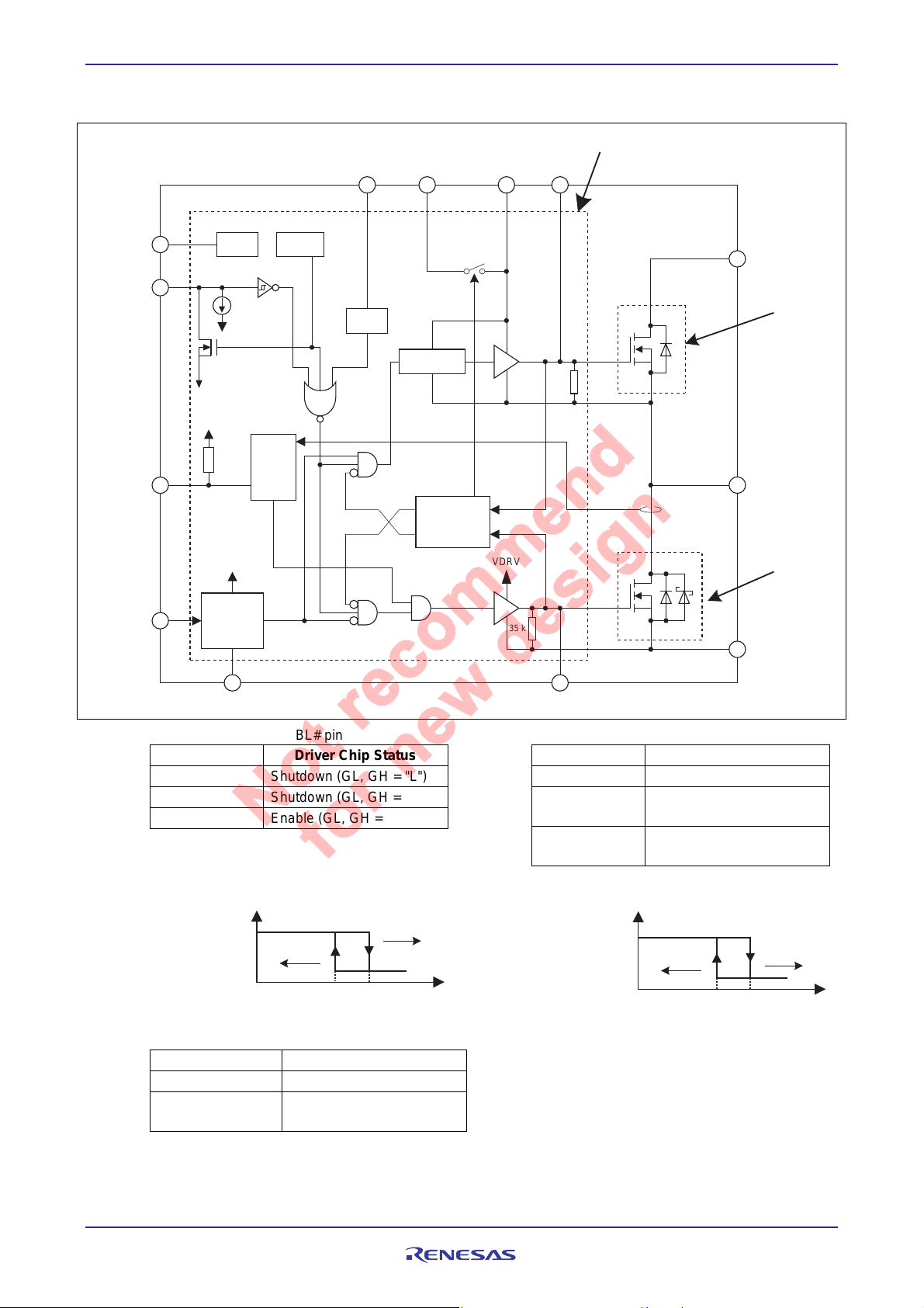
Block Diagram
Driver Chip
THWN
DISBL#
ZCD_EN#
PWM
THWN THDN
2 μA
CGND
CGND
VCIN
160 k
VCIN
Input Logic
(TTL Level)
(3 state in)
Zero
Current
Det.
VCIN
UVL
VDRV
Level Shifter
Overlap
Protection.
& Logic
BOOT GH
Boot
SW
VDRV
VIN
High Side
MOS FET
20 k
VSWH
Low Side
MOS FET
35 k
PGND
GLCGND
Notes: 1. Truth table for the DISBL# pin 2. Truth table for the ZCD_EN# pin
DISBL# Input Driver Chip Status
"L" Shutdown (GL, GH = "L")
"Open" Shutdown (GL, GH = "L")
"H" Enable (GL, GH = "Active")
ZCD_EN# Input Driver Chip Status
"L" "Diode Emulation Mode"
"Open"
"Continuous Conduction
Mode"
"H"
"Continuous Conduction
Mode"
3. Output signal from the UVL block 4. Output signal from the THWN block
VHVL
For active
VCIN
Thermal Warning
Logic Level
"H"
"L"
Normal
operating
Thermal
Warning
T
(°C)
IC
TwarnHTwarnL
UVL output
Logic Level
"H"
For shutdown
"L"
5. Truth table for the THDN block
Driver IC Temp. Driver Chip Status
< 150°C Enable (GL, GH = "Active")
> 150°C
Shutdown (GL, GH = "L")
(latch-off)
R07DS0201EJ0100 Rev.1.00 Page 2 of 15
Jan 25, 2011
R2J20656ANP Preliminary
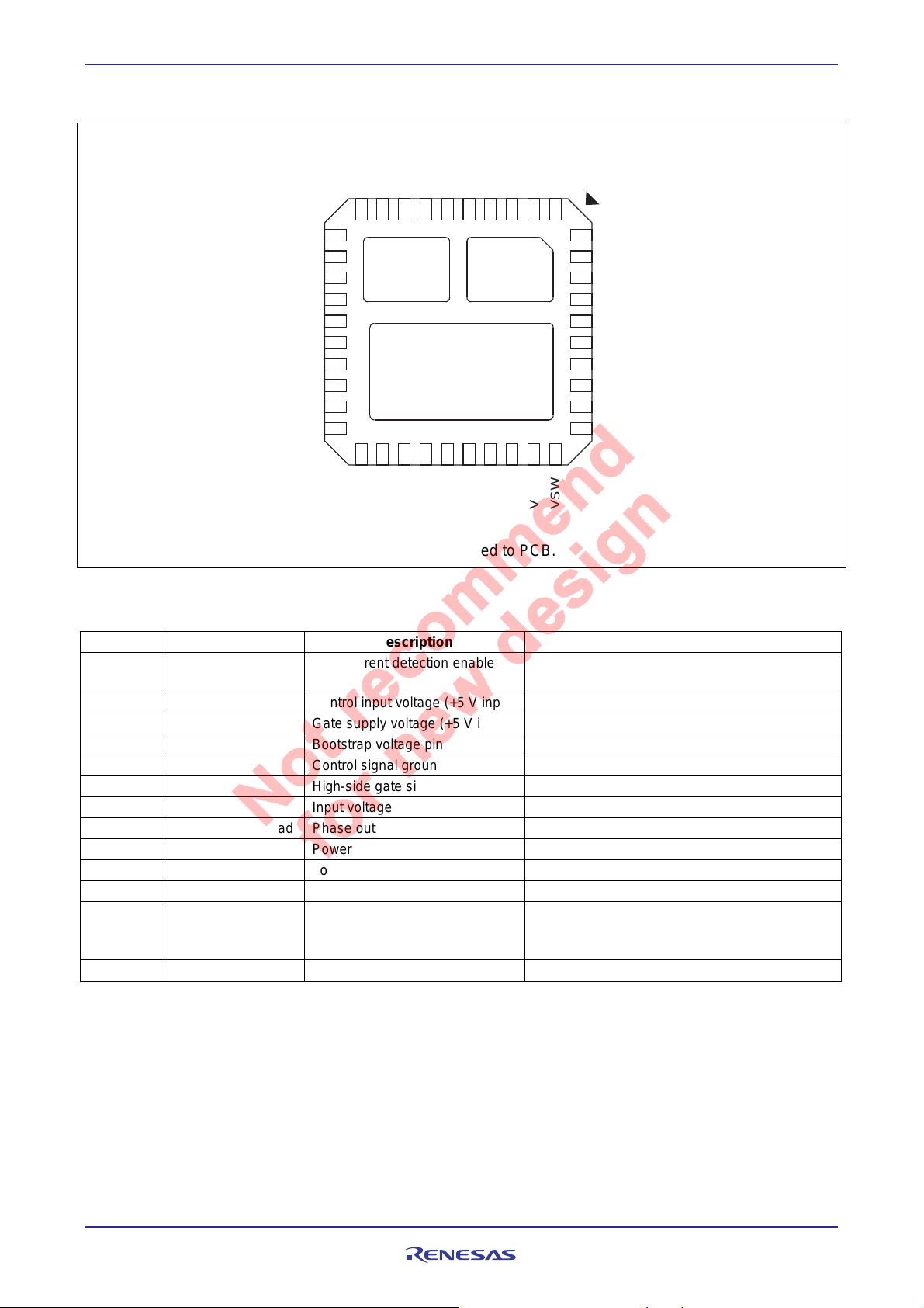
Pin Arrangement
VIN
VIN
VIN
VSWHGHCGND
1098765432
11
VIN PWM
12
VIN
13
VIN
14
VIN
VSWH
PGND
PGND
PGND
PGND
PGND VSWH
15
16
17
18
19
20
VIN
VSWH
21 22 23 24 25 26 27 28 29 30
PGND
PGND
PGND
PGND
PGND
PGND
BOOT
VDRV
CGND
PGND
PGND
VCIN
VSWH
(Top view)
Note: All die-pads (three pads in total) should be soldered to PCB.
Pin Description
ZCD_EN#
1
40
39
38
37
36
35
34
33
32
31
VSWH
DISBL#
THWN
CGND
GL
VSWH
VSWH
VSWH
VSWH
Pin Name Pin No. Description Remarks
ZCD_EN# 1 Zero current detection enable
When asserted "L" signal, zero crossing
detection is enabled
VCIN 2 Control input voltage (+5 V input) Driver Vcc input
VDRV 3 Gate supply voltage (+5 V input) 5 V gate drive
BOOT 4 Bootstrap voltage pin To be supplied +5 V through internal switch
CGND 5, 37, Pad Control signal ground Should be connected to PGND externally
GH 6 High-side gate signal Pin for monitor
VIN 8 to 14, Pad Input voltage
VSWH 7, 15, 29 to 35, Pad Phase output/Switch output
PGND 16 to 28 Power ground
GL 36 Low-side gate signal Pin for monitor
THWN 38 Thermal warning Thermal warning when over 115°C
DISBL# 39 Signal disable
Disabled when DISBL# is "L".
This Pin is pulled low when internal IC over the
thermal shutdown level, 150°C.
PWM 40 PWM drive logic input 5 V logic input
R07DS0201EJ0100 Rev.1.00 Page 3 of 15
Jan 25, 2011
R2J20656ANP Preliminary
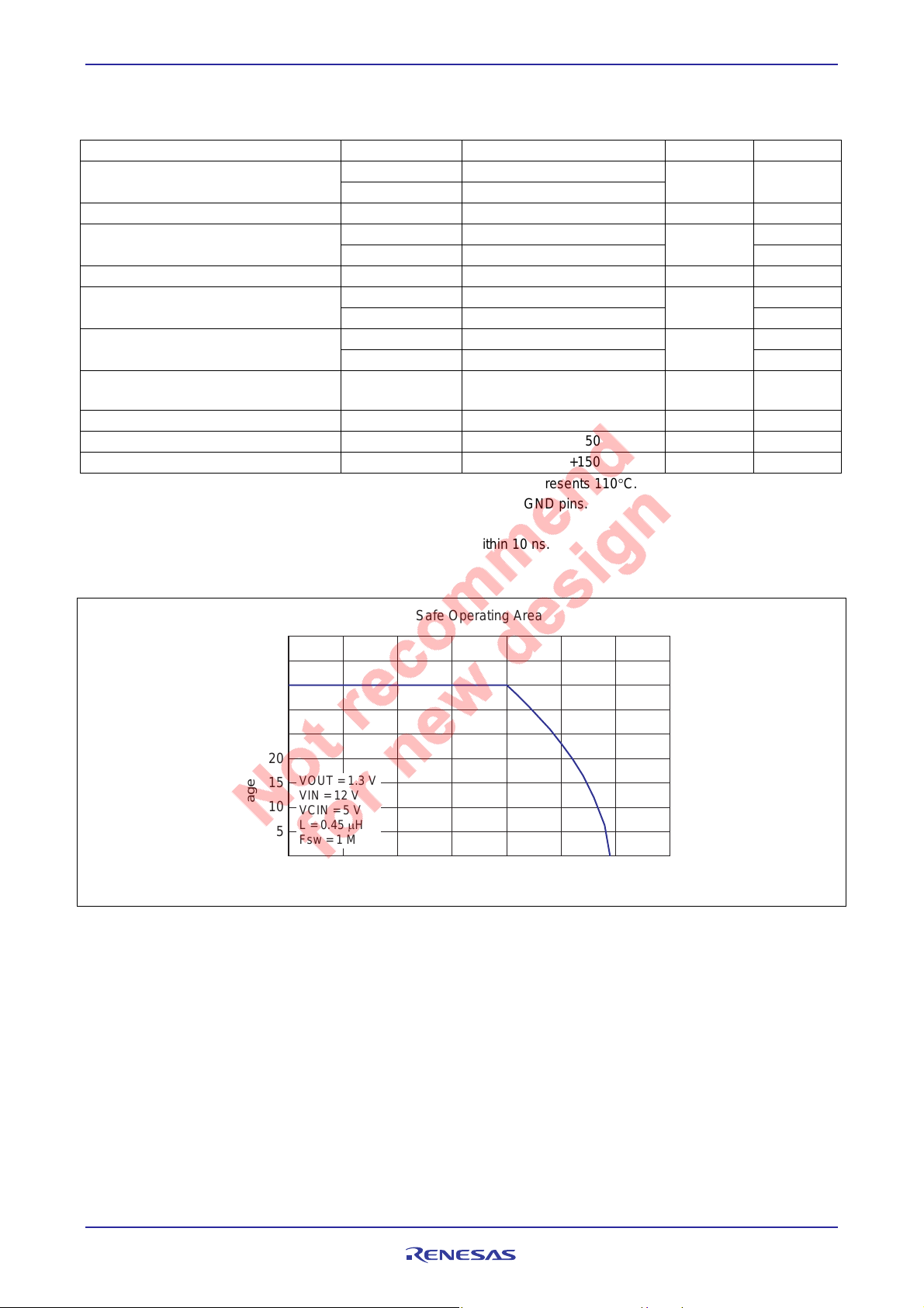
Absolute Maximum Ratings
(Ta = 25°C)
Item Symbol Rating Units Note
Pt(25) 25 Power dissipation
Pt(110) 8
Average output current Iout 35 A
VIN(DC) –0.3 to +27 2 Input voltage
VIN(AC) 30
Supply voltage & Drive voltage VCIN & VDRV –0.3 to +6 V 2
VSWH(DC) 27 2 Switch node voltage
VSWH(AC) 30
VBOOT(DC) 32 2 BOOT voltage
VBOOT(AC) 36
I/O voltage
THWN/THDN current Ithwn, Ithdn 0 to 1.0 mA
Operating junction temperature Tj-opr –40 to +150 °C
Storage temperature Tstg –55 to +150 °C
Notes: 1. Pt(25) represents a PCB temperature of 25°C, and Pt(110) represents 110C.
2. Rated voltages are relativ e to voltages on the CGND and PGND pins.
3. For rated current, (+) indicates inflow.
4. The specification values indicated "AC" are limited within 10 ns.
5. VCIN + 0.3 V < 6 V
Vpwm, Vdisble,
Vlsdbl, Vthwn
–0.3 to VCIN + 0.3 V 2, 5
W 1
V
2, 4
V
2, 4
V
2, 4
Safe Operating Area
45
40
35
30
25
20
VOUT = 1.3 V
15
VIN = 12 V
10
VCIN = 5 V
L = 0.45 μH
Average Output Current (A)
5
Fsw = 1 MHz
0
0 25 50 75 100 125 150 175
PCB Temperature (°C)
R07DS0201EJ0100 Rev.1.00 Page 4 of 15
Jan 25, 2011
R2J20656ANP Preliminary
Recommended Operating Condition
Item Symbol Rating Units Note
Input voltage VIN 4.5 to 22 V
Supply voltage & Drive voltage VCIN & VDRV 4.5 to 5.5 V
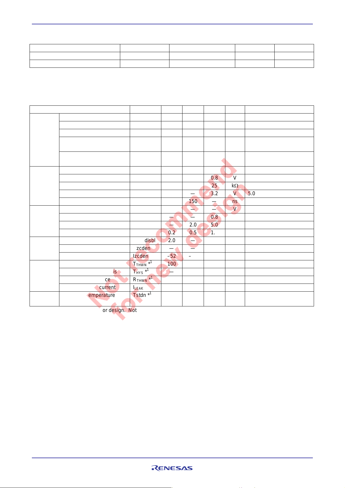
Electrical Characteristics
(Ta = 25°C, VCIN = 5 V, VDRV = 5 V, VSWH = 0 V, unless otherwise specified)
Item Symbol Min Typ Max Units Test Conditions
Supply
PWM
input
DISBL#
input
ZCD_EN#
Thermal
warning
Thermal
shutdown
Note: 1. Reference values for design. Not 100% tested in production.
VCIN start threshold VH 4.1 4.3 4.5 V
VCIN shutdown threshold VL 3.6 3.8 4.0 V
UVLO hysteresis dUVL — 0.5 — V VH – VL
VCIN operating current I
— 49 — mA
CIN
f
PWM
= 1 MHz,
Ton_pwm = 120 ns
VCIN disable current I
— — 150 A
CIN-DISBL
DISBL# = 0 V,
PWM = ZCD_EN# = Open
PWM input high level V
PWM input low level V
PWM input resistance R
PWM input tri-state range V
Shutdown hold-off time t
Enable level V
Disable level V
Input current I
THDN on resistance R
4.0 — — V 5.0 V PWM interface
H-PWM
— — 0.8 V
L-PWM
6.5 12.5 25 k PWM = 1 V
IN-PWM
1.5 — 3.2 V 5.0 V PWM interface
IN-tri
HOLD-OFF
ENBL
DISBL
DISBL
THDN
1
*
— 150 — ns
2.0 — — V
— — 0.8 V
— 2.0 5.0 A DISBL# = 1 V
*1 0.2 0.5 1.0 k DISBL# = 0.2 V
ZCD disable level Vzcddisbl 2.0 — — V
ZCD enable level Vzcden — — 0.8 V
Input current Izcden –52 –25 –12 A ZCD_EN# = 1 V
Warning temperature T
Temperature hysteresis T
THWN on resistance R
THWN leakage current I
Shutdown temperature Tstdn *
*1 100 115 130 °C Driver IC temperature
THWN
*1 — 15 — °C
HYS
*1 0.2 0.5 1.0 k THWN = 0.2 V
THWN
— — 1.0 A THWN = 5 V
LEAK
1
130 150 — °C Driver IC temperature
R07DS0201EJ0100 Rev.1.00 Page 5 of 15
Jan 25, 2011
R2J20656ANP Preliminary
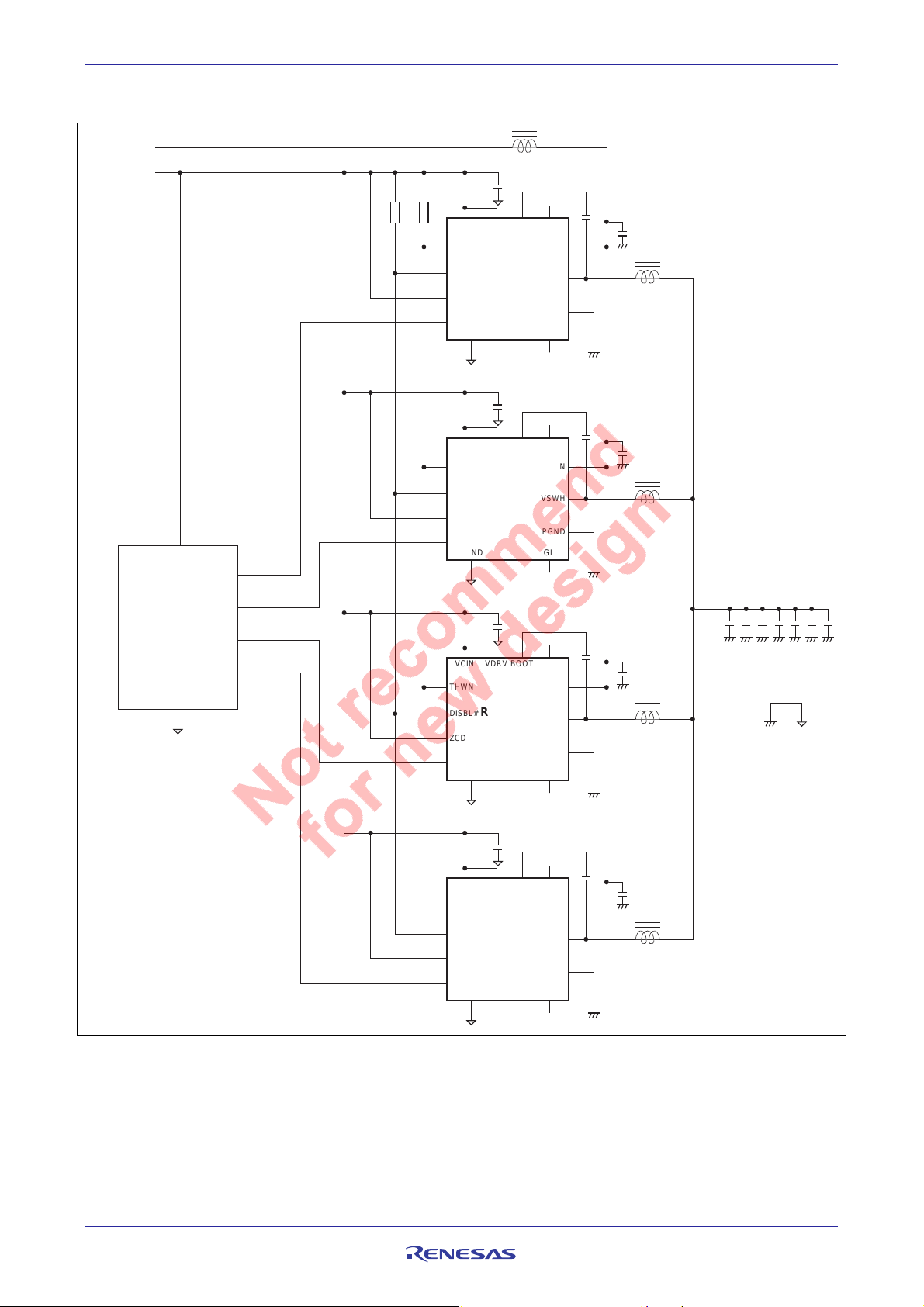
Typical Application
4.5 to 22 V
+5 V
PWM
Control
Circuit
PWM1
PWM2
PWM3
PWM4
VCIN
THWN
DISBL#
ZCD_EN#
PWM
CGND GL
VCIN
THWN
DISBL#
ZCD_EN#
PWM
CGND GL
VCIN
THWN
DISBL#
ZCD_EN#
PWM
CGND GL
BOOT
R2J20656
ANP
BOOT GHVDRV
R2J20656
ANP
BOOT
R2J20656
ANP
GHVDRV
VIN
VSWH
PGND
VIN
VSWH
PGND
+1.3 V
GHVDRV
VIN
VSWH
Power GND Signal GND
PGND
VCIN
THWN
DISBL#
ZCD_EN#
PWM
CGND GL
BOOT
R2J20656
ANP
GHVDRV
VIN
VSWH
PGND
R07DS0201EJ0100 Rev.1.00 Page 6 of 15
Jan 25, 2011
 Loading...