

Page 1
REJ11J0038-0002
PRELIMINARY
Notice: This is not a final specification.
Some parametric limits are subject to change.
32
SH7216 CPU Board
R0K572167
User's Manual
Renesas 32-Bit RISC Microcomputers
SuperH TM RISC engine Family / SH7216 Group
Rev. 0.02
Issued on: Mar. 27, 2009
Page 2

Page 3

Table of Contents
Chapter 1 Overview .............................................................................................................................1-1
1.1 Introduction................................................................................................................................................................. 1-2
1.2 Configuration .............................................................................................................................................................. 1-2
1.3 Board Specifications................................................................................................................................................... 1-3
1.4 Exterior....................................................................................................................................................................... 1-4
1.5 Block Diagram ............................................................................................................................................................ 1-5
1.6 Component Layout ..................................................................................................................................................... 1-6
1.7 Memory Maps............................................................................................................................................................. 1-9
1.8 Absolute Maximum Ratings...................................................................................................................................... 1-11
1.9 Operating Conditions................................................................................................................................................ 1-11
Chapter 2 Functions ............................................................................................................................2-1
2.1 Overview of Functions ................................................................................................................................................ 2-2
2.2 CPU............................................................................................................................................................................ 2-3
2.3 External Memory ........................................................................................................................................................ 2-4
2.3.1 SDRAM ............................................................................................................................................................. 2-4
2.4 Serial Port Interface.................................................................................................................................................... 2-5
2.5 I/O Ports ..................................................................................................................................................................... 2-6
2.6 USB Interface ............................................................................................................................................................. 2-9
2.7 RCAN Interface ........................................................................................................................................................ 2-10
2.8 Ethernet Interface..................................................................................................................................................... 2-11
2.9 Interrupt Switches..................................................................................................................................................... 2-12
2.10 E10A-USB Interface ............................................................................................................................................... 2-13
2.11 Power Supply Module............................................................................................................................................. 2-14
2.12 Clock Module.......................................................................................................................................................... 2-15
2.13 Reset Module ......................................................................................................................................................... 2-15
Chapter 3 Operating Specifications .....................................................................................................3-1
3.1 Connectors ................................................................................................................................................................. 3-2
3.1.1 H-UDI Port Connectors (J2 and J3) .................................................................................................................. 3-4
3.1.2 Serial Port Connector (J7)................................................................................................................................. 3-6
3.1.3 Power Supply Connector (J4) ........................................................................................................................... 3-7
3.1.4 SH7216 External Power Supply Connectors (J8, J9, J12, J13) ........................................................................ 3-8
3.1.5 DC Power Supply Jack (J6) ............................................................................................................................ 3-10
3.1.6 Expansion Connectors (JA1, JA2, JA3, JA5, JA6) .......................................................................................... 3-11
3.1.7 RCAN Port Connector (J10)............................................................................................................................ 3-18
3.1.8 USB Port Connector (J5)................................................................................................................................. 3-19
3.1.9 LAN Port Connector (J1)................................................................................................................................. 3-20
3.1.10 GND Connector (J11).................................................................................................................................... 3-21
3.2 Switches and LEDs .................................................................................................................................................. 3-22
3.2.1 USB Boot Clock Switch Jumper (JP1) ............................................................................................................ 3-23
3.2.2 External Power Supply Switch Jumpers (JP7, JP3, JP8, JP9)........................................................................ 3-24
Rev. 0.02 Mar. 27, 2009
REJ11J0038-0002
(i)
Page 4

3.2.3 Serial Port Switch Jumpers (JP2 and JP4)...................................................................................................... 3-25
3.2.4 RCAN Port Switch Jumpers (JP5 and JP6)..................................................................................................... 3-26
3.2.5 Switches and LEDs ......................................................................................................................................... 3-27
3.2.6 Jumper/Switch Setting when Using the Development Tools ........................................................................... 3-30
3.3 Dimensions............................................................................................................................................................... 3-31
Appendix.............................................................................................................................................A-1
SCHEMATICS
Rev. 0.02 Mar. 27, 2009
REJ11J0038-0002
(ii)
Page 5

Chapter 1Overview
Chapter 1
Overview
1-1
Page 6
1
1.1 Introduction
1.1 Introduction
The R0K572167 is a CPU board designed for evaluating the features and performance of the SH7216 Group of
Renesas Technology single-chip RISC microcomputers (MCUs). It is also used for developing and evaluating
application software for these MCUs. The MCU’s data bus, address bus, and internal peripheral pins are connected
to expansion connectors on the R0K572167 to allow for timing evaluation with peripherals using measurement
instruments, and the development of the expansion board according to its application. The Renesas Technology
E10A-USB on-chip emulator can be connected to the R0K572167.
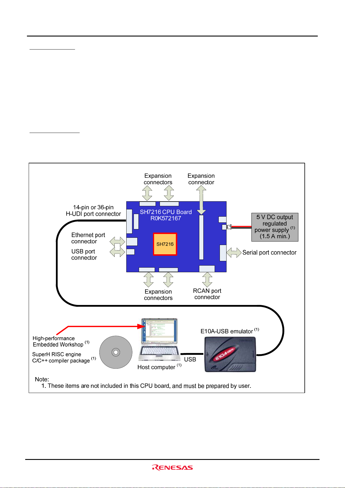
1.2 Configuration
The following figure shows an example of a system configuration using the R0K572167.
Overview
Figure 1.2.1 Configuration using the R0K572167
Rev. 0.02 Mar. 27, 2009 1-2
REJ1 1J0038-0002
Page 7

1
1.3 Board Specifications
The following table lists the specifications of the R0K572167.
Table 1.3.1 Board Specifications
Item Description
SH7216
• Input (XIN) clock: 12.5 MHz
• CPU clock: 200 MHz max.
CPU
Memory • SDRAM: 16 MB (16-bit bus x 1)
Connectors
LEDs
Switches
Board specifications
• Bus clock: 50 MHz max.
• Internal memory
¾ Flash memory: 1024 KB
¾ RAM: 128 KB
¾ FLD(flash memory for data): 32 KB
• Expansion connectors (bus, I/O, VCC, GND)
• USB port connector (Series-B receptacle)
• Ethernet port connector (8-pin, RJ-45)
• Serial port connector (D-sub, 9-pin)
• RCAN port connector (D-sub, 9-pin)
• 14-pin H-UDI port connector
• 36-pin H-UDI port connector
• Power supply LED: 1
• User LEDs: 6
• PHY-LSI LEDs: 5
• Reset switch: 1
• NMI switch: 1
• IRQ6 switch: 1
• System setting DIP switches: 4/package
• User DIP switches: 4/package
• PHY-LSI setting DIP switches: 6/package
• Dimensions: 130 mm x 175 mm
• Mounting form: 4-layer, double-sided
• Number of boards: 1
Overview
1.3 Board Specifications
Rev. 0.02 Mar. 27, 2009 1-3
REJ1 1J0038-0002
Page 8

1
1.4 Exterior
The following figure shows the exterior of the R0K572167.
Overview
1.4 Exterior
Figure 1.4.1 R0K572167 Exterior
Rev. 0.02 Mar. 27, 2009 1-4
REJ1 1J0038-0002
Page 9

1
1.5 Block Diagram
The following figure shows the block diagram of the R0K572167.
Overview
1.5 Block Diagram
Ethernet port
connector
RCAN port
connector
XTAL
(25 MHz)
RCAN
PHY
LSI
H-UDI port connector
(36-pin)
H-UDI
AUD
Bus
switch
Expansion connector
Figure 1.5.1 R0K572167 Block Diagram
H-UDI port connector
(14-pin)
SH7216
(200 MHz)
8/16 bits
8/16 bits
Serial port
connector
SCI1
USB
USBEXTAL
(48.0 MHz)
SDRAM
EXTAL
(12.5 MHz)
External bus 50 MHz max.
16 MB
USB port
connector
16 bits
SH7216 CPU Board
R0K572167
Rev. 0.02 Mar. 27, 2009 1-5
REJ1 1J0038-0002
Page 10

1
1.6 Component Layout
Figure 1.6.1 and Figure 1.6.2 show the layout of major components on the R0K572167.
7
14
1
8
Overview
1.6 Component Layout
Figure 1.6.1 R0K572167 Component Layout (Top View of the Component Side)
Rev. 0.02 Mar. 27, 2009 1-6
REJ1 1J0038-0002
Page 11

1
Overview
1.6 Component Layout
Figure 1.6.2 R0K572167 Component Layout (Top Vie w of the Solder Si de)
Rev. 0.02 Mar. 27, 2009 1-7
REJ1 1J0038-0002
Page 12

Overview
1
The following table lists the major components on the R0K572167.
Table 1.6.1 Major Components on the R0K572167
Symbol Name Remarks
U1 CPU SH7216 (Renesas)
U5 SDRAM MT48LC8M16A2P-7E (Micron)
U14 RS-232C driver SP3232ECA-L (Sipex)
U16 RCAN driver HA13721RPJE (Renesas)
U11 3.3 V regulator LM2738-YMY 550 KHz (NS)
U13 1.55 V regulator Optional
U9 Reset IC M51957BFP (Renesas)
X1 Crystal unit
X2 Resonator (Ceralock) CSTCZ48M0X11R**-B0 (Murata)
X3 Oscillator
J2 36-pin H-UDI connector DX10M-36SE (Hirose)
J3 14-pin H-UDI connector HTST-107-01-T-DV (Samtec)
J7 Serial port connector 154188 (ERNI)
J4 Power supply connector S2B-XH-A (J.S.T.)
J8 External power supply connector Optional A2-2PA-2.54DSA (Hirose)
J9 External power supply connector Optional A2-2PA-2.54DSA (Hirose)
J12 External power supply connector Optional A2-2PA-2.54DSA (Hirose)
J13 External power supply connector Optional A2-2PA-2.54DSA (Hirose)
J6 DC power supply jack KLDX-SMT2-0202-A (Kycon)
JA1,
JA2
JA3 50-pin expansion connector Optional FCN-744Q050-AU/0 (FUJITSU)
JA5,
JA6
J14 USB port connector
J13 RCAN port connector 154236 (ENRI)
J1 Ethernet port connector RJ-45 TLA-6T718 (TDK)
LED1 to
LED5
LED6 Power supply LED Blue
LED7 to
LED12
SW4 Power supply switch MS-12AAH1 (Nikkai)
SW3 Reset switch B3SN-3012 (OMRON)
SW5 User DIP switches A6S-4104 (4/package) (OMRON)
SW1 System setting DIP switches A6S-4104 (4/package) (OMRON)
SW2 PHY-LSI setting DIP switches A6S-6104 (6/package) (OMRON)
SW6 NMI switch B3SN-3012 (OMRON)
SW7 IRQ6 switch B3SN-3012 (OMRON)
26-pin expansion connectors Optional FCN-744Q026-AU/0 (FUJITSU)
24-pin expansion connectors Optional FCN-744Q024-AU/0 (FUJITSU)
PHY-LSI LEDs Yellow
User LEDs Green
CX5032GB 12500
(Kyocera Kinseki)
SG-8002JF_25MHz_PCC
(Epson Toyocom)
UBB-4R-D14T-4D(SN)(LF) (J.S.T.)
Recommended Optional Components
(Manufacturer Name and Part Number)
LM2738-YMY 550 kHz (NS)
1.6 Component Layout
Rev. 0.02 Mar. 27, 2009 1-8
REJ1 1J0038-0002
Page 13

1
1.7 Memory Maps
Figure 1.7.1 and Figure 1.7.2 show memory map examples of the SH7216 and R0K5721 67.
SH7216 Logic Space
in MCU Mode 3
(Single-chip Mode)
H'0000 0000
H'000F FFFF
H'0010 0000
Internal ROM (1024 KB)
H'0000 0000
H'000F FFFF
H'0010 0000
Overview
1.7 Memory Map
R0K572167 Memory Map
Internal ROM (1024 KB)
H'FFF7 FFFF
H'FFF8 0000
H'FFF9 FFFF
H'FFFA 0000
Reserved
Internal RAM (128 KB)
Reserved
H'FFF7 FFFF
H'FFF8 0000
H'FFF9 FFFF
H'FFFA 0000
Reserved
Internal RAM (128 KB)
Reserved
H'FFFD FFFF
H'FFFE 0000
H'FFFF FFFF
Rev. 0.02 Mar. 27, 2009 1-9
REJ1 1J0038-0002
Peripheral I/O
Figure 1.7.1 SH7216 Memory Map Example (MCU Mode 3)
H'FFFD FFFF
H'FFFE 0000
H'FFFF FFFF
Peripheral I/O
Page 14

1
H'0000 0000
H'000F FFFF
H'0010 0000
H'01FF FFFF
H'0200 0000
H'03FF FFFF
H'0400 0000
H'07FF FFFF
H'0800 0000
H'0BFF FFFF
H'0C00 0000
H'0FFF FFFF
H'1000 0000
H'13FF FFFF
H'1400 0000
H'17FF FFFF
H'1800 0000
H'1BFF FFFF
H'1C00 0000
H'1FFF FFFF
H'2000 0000
SH7216 Logic Space
in MCU Mode 2
(Internal ROM Enabled Mode)
Internal ROM (1024 KB)
Reserved
CS0 space
CS1 space
CS2 space
CS3 space
CS4 space
CS5 space
CS6 space
CS7 space User area
H'0000 0000
H'000F FFFF
H'0010 0000
H'01FF FFFF
H'0200 0000
H'03FF FFFF
H'0400 0000
H'07FF FFFF
H'0800 0000
H'0BFF FFFF
H'0C00 0000
H'0FFF FFFF
H'1000 0000
H'13FF FFFF
H'1400 0000
H'17FF FFFF
H'1800 0000
H'1BFF FFFF
H'1C00 0000
H'1FFF FFFF
H'2000 0000
Overview
1.7 Memory Map
R0K572167 Memory Map
Internal ROM (1024 KB)
Reserved
User area
User area
User area
SDRAM (16 MB)
User area
User area
User area
User area
H'FFF7 FFFF
H'FFF8 0000
H'FFF8 7FFF
H'FFF8 8000
H'FFFB FFFF
H'FFFC 0000
H'FFFC FFFF
H'FFFD 0000
H'FFFD FFFF
H'FFFE 0000
H'FFFF FFFF
Reserved
H'FFF7 FFFF
Internal RAM (128 KB)
Reserved
SDRAM mode setting
Reserved
Peripheral I/O
Figure 1.7.2 SH7216 Memory Map Example (MCU Mode 2)
H'FFF8 0000
H'FFF8 7FFF
H'FFF8 8000
H'FFFB FFFF
H'FFFC 0000
H'FFFC FFFF
H'FFFD 0000
H'FFFD FFFF
H'FFFE 0000
H'FFFF FFFF
Reserved
Internal RAM (128 KB)
Reserved
SDRAM mode setting
Reserved
Peripheral I/O
Rev. 0.02 Mar. 27, 2009 1-10
REJ1 1J0038-0002
Page 15

1
1.8 Absolute Maximum Ratings
1.8 Absolute Maximum Ratings
The following table lists the absolute maximum ratings of the R0K572167.
Table 1.8.1 R0K572167 Absolute Maximum Ratings
Symbol Parameter Value Remarks
5VCC 5 V system power supply voltage -0.3 to 6.0 V Reference voltage: VSS
3VCC 3.3 V system power supply voltage -0.3 to 4.6 V Reference voltage: VSS
1.5VCC 1.5 V system power supply voltage -0.3 to 2.3 V Reference voltage: VSS
T
Operating temperature 0°C to 50°C Do not expose to condensation or corrosive gas
opr
T
Storage temperature -10°C to 60°C Do not expose to condensation or corrosive gas
stg
Note: Temperature refers to the air temperature in the vicinity of the board.
1.9 Operating Conditions
The following table lists the operating conditions for the R0K572167.
Overview
Table 1.9.1 R0K572167 Operating Conditions
Symbol Items Value Remarks
5VCC 5 V system power supply voltage 4.5 to 5.5 V Reference voltage: VSS
3VCC 3.3 V system power supply voltage 3.0 to 3.6 V Reference voltage: VSS
1.5VCC 1.5 V system power supply voltage 1.5 to 1.6 V Reference voltage: VSS
- Maximum current consumption 1.5 A max.
T
Operating temperature 0°C to 50°C Do not expose to condensation or corrosive gas
opr
Rev. 0.02 Mar. 27, 2009 1-1 1
REJ1 1J0038-0002
Page 16

1
Overview
1.9 Operating Conditions
This page intentionally left blank.
Rev. 0.02 Mar. 27, 2009 1-12
REJ1 1J0038-0002
Page 17

Chapter 2Functions
Chapter 2
Functions
2-1
Page 18

2
2.1 Overview of Functions
The R0K572167 includes the function modules listed in the following table.
Table 2.1.1 R0K572167 Function Modules
Section Function Description
SH7216
• Input (XIN) clock: 12.5 MHz
• CPU clock: 200 MHz max.
2.2 CPU
2.3 External memory
2.4 Serial port interface Connects the SH7216 SCI1 pin to the serial port connector
2.5 I/O ports Connect to the SH7216 I/O ports
2.6 USB interface
2.7 RCAN interface
2.8 Ethernet interface
2.9 Interrupt switch Connects to the NMI pin and IRQ6 pin
2.10 E10A-USB interface
2.11 Power supply module Controls the R0K572167 system power supply
2.12 Clock module
2.13 Reset module Resets the devices mounted on the R0K572167
- Operating specifications
• Bus clock: 50 MHz max.
Internal memory
• Flash memory: User MAT: 1024 KB
• FLD: 32 KB
• RAM: 128 KB
SDRAM: 16 MB (16-bit bus)
Connects the SH7216 USB pin to the USB port connector
- Clock source
¾ USB: 48 MHz ceramic resonator
Connects the SH7216 RCAN pin to the RCAN port connector via the
RCAN transceiver
Connects the SH7216 Ethernet pin to the Ethernet port connector (pulse
transformer included) via the PHY-LSI
Connects the SH7216 H-UDI/AUD pin to the H-UDI port connector
* Do not use the AUD pin when using the Ethernet interface.
Controls the system clock
- Clock source
¾ Crystal unit: 12.5 MHz
Connectors, switches, and LEDs
• SH7216 expansion connectors
• Switches and LEDs
• H-UDI port connectors
• Serial port connector
• USB port connector
• RCAN port connector
• Ethernet port connector
Refer to Chapter 3 for details.
Functions
2.1 Overview of Functions
Rev. 0.02 Mar. 27, 2009 2-2
REJ11J0038-0002
Page 19
Functions
2
2.2 CPU
The R0K572167 includes the SH7216, the 32-bit RISC MCU that operates with a maximum frequency of 200 MHz. The
SH7216 has 1024 KB of flash memory, 32 KB of EEPROM, and 128 KB of RAM to support various applications such as
data processing and equipment control.
The SH7216 can operate at a CPU clock frequency of 200 MHz (external bus is a maximum 50 MHz) when the input
clock is 12.5 MHz on the R0K572167.
The following figure shows a block diagram of the SH7216 on the R0K572167.
SH7216
Clocks
System
Control
User LEDs
IIC
USB port
connector (J5)
GPIO, control signal,
MTU2/2S, interrupt, etc.
RCAN port
connector (J10)
Serial port
connector (J7)
H-UDI connectors
Mode switch
EXTAL
XTAL
PA18/CK
RES
NMI
WDTOVF
PE9/TIOC3B/DACK2/TX_EN
PE11/TIOC3D/DACK3/MII_TXD0
PE12/TIOC4A/MII_TXD1
PE13/TIOC4B/MRES/MII_TXD2
PE14/DACK0/TIOC4C/MI_TXD3
PE15/DACK1/TIOC4D/IRQOUT/TX_ER
PB2/A18/RASL/IRQ2/RXD3/TIOC0B/BACK/FRAME
PB12/SCL/POE1/IRQ2
PB13/SDA/POE2/IRQ3
USBXTAL
USBEXTAL
PB14/IRQ6
VBUS
USD+
USDPB15/(PUPD)/IRQ7
PE1/TIOC0B/TIOC4BS/TEND0/MDC
PE2/TIOC0C/TIOC4CS/DREQ1/WOL
PE3/TIOC0D/TIOC4DS/TEND1/COL
PE4/TIOC1A/SCK3/POE8/IRQ4/CRS
PE5/TIOC1B/TIOC3BS/TXD3/MDIO
PE6/TIOC2A/TIOC3DS/RXD3
PA21/RD/CKE/BACK/POE3/IRQ5/SCK1/FRAME
PA20/WRL-DQMLL/CASU/BREQ/POE4/IRQ6/TXD1/AH
PA19/WRH-DQMLU/RASU/WAIT/POE8/IRQ7/RXD1/BS
PA17/RD
PA16/WRL-DQMLL
PA15/WRH-DQMLU
PA14/WRHH-DQMUU/RASL
PA13/WRHL-DQMUL/CASL
PB7/A23/IRQ7/SCK4/TCLKC/TEND0
PB8/A24/CS2/TCLKB/DREQ0/RXD4
PB9/A25/CS3/TCLKA/DACK0/TXD4
PB10/RXD2/CS6/CS2/CS0/IRQ0
PB11/TXD2/CS7/CS3/CS1/IRQ1
PA0/RXD0/CS0/CRx0/IRQ4/RX_CLK
PA1/TXD0/CS1/CTx0/IRQ5/MII_RXD0
PA2/SCK0/SSL0/CS2/TCLKD/MII_RXD1
PA3/RXD1/MISO/CS3/TCLKC/MII_RXD2
PA4/TXD1/MOSI/CS4/TCLKB/MII_RXD3
PA5/SCK1/RSPCK/CS5/TCLKA/RX_ER
PE7/TIOC2B/UBCTRG/RXD2/SSL1/RX_DV
PE8/TIOC3A/DREQ2/SCK2/SSL2/EXOUT
PE10/TIOC3C/DREQ3/TXD2/SSL3/TX_CLK
PE0/TIOC0A/TIOC4AS/DREQ0/LINKSTA
TDI
TDO
TCK
TMS
TRST
ASEMD0
FWE/ASEBRKAK
MD1
MD0
/ASEBRK
PC10/A10/TIOC1A/CRx0/RXD0
PB1/A17/IRQOUT/ADTRG/TIOC0A/IRQ1
PB3/A19/CASL/IRQ3/TXD3/TIOC0C/BREQ/AH
PB4/A20/IRQ4/SCK3/TIOC0D/WAIT/BACK/BS
PB6/A22/IRQ6/TXD0/TCLKD/WAIT
PD16/D16/IRQ0/POE0/UBCTRG/AUDATA0
PD17/D17/IRQ1/POE4/ADTRG/AUDATA1
PD18/D18/IRQ2/AUDATA2/MDIO
PD19/D19/IRQ3\/AUDATA3/LINKSTA
PD20/D20/IRQ4/AUDSYNC/MDC
PD21/D21/IRQ5/TEND1/AUDCK/EXOUT
PD26/D26/TIOC4BS/MII_RXD0
PD27/D27/TIOC4AS/MII_RXD1
PD28/D28/TIOC3DS/MII_RXD2
PD29/D29/TIOC3BS/MII_RXD3
PD30/D30/TIOC3CS/SSL3/RX_ER
PD31/D31/TIOC3AS/SSL2/RX_DV
PA12/IRQ0/TIC5U/CS0/SSL1/TX_CLK
PA11/IRQ1/TIC5V/CS1/TX_EN/CRx0/RXD0
PA10/IRQ2/TIC5W/CS2/MII_TXD0/CTx0/TXD0
PA9/IRQ3/TCLKD/CS3/MII_TXD1/SSL0/SCK0
PA8/IRQ4/TCLKC/CS4/MII_TXD2/MISO/RXD1
PA7/IRQ5/TCLKB/CS5/MII_TXD3/MOSI/TXD1
PA6/IRQ6/TCLKA/CS6/TX_ER/RSPCK/SCK1
PC0/A0/POE0/IRQ4
PC8/A8/CRx0/RXD0
PC9/A9/CTx0/TXD0
PC11/A11/TIOC1B/CTx0/TXD0
PC13/A13/IRQ0/TCLKB
PC14/A14/IRQ1/TCLKC
PC15/A15/IRQ2/TCLKD
PB0/A16/IRQ0/RDWR/TIOC2A
PB5/A21/IRQ5/RXD0/BREQ
PD2/D2/TIC5U/RXD2
PD3/D3/TIC5V/TXD2
PD4/D4/TIC5W/SCK2
PD10/D10/TIOC3BS
PD11/D11/TIOC3DS
PD12/D12/TIOC4AS
PD13/D13/TIOC4BS
PD14/D14/TIOC4CS
PD15/D15/TIOC4DS
PD22/D22/IRQ6/DREQ1/WOL
PD23/D23/IRQ7/DACK1/COL
PD24/D24/TIOC4DS/CRS
PD25/D25/TIOC4CS/RX_CLK
PC1/A1
PC2/A2
PC3/A3
PC4/A4
PC5/A5
PC6/A6
PC7/A7
PC12/A12/TCLKA
PD0/D0
PD1/D1
PD5/D5/TIC5US
PD6/D6/TIC5VS
PD7/D7/TIC5WS
PD8/D8/TIOC3AS
PD9/D9/TIOC3CS
PF0/AN0
PF1/AN1
PF2/AN2
PF3/AN3
PF4/AN4
PF5/AN5
PF6/AN6
PF7/AN7
Address bus
Data bus
Ethernet
A/D
User DIP
switches
(SW5)
2.2 CPU
AUD
RSPI
Figure 2.2.1 SH7216 Block Diagram
Rev. 0.02 Mar. 27, 2009 2-3
REJ11J0038-0002
Page 20
2
2.3 External Memory
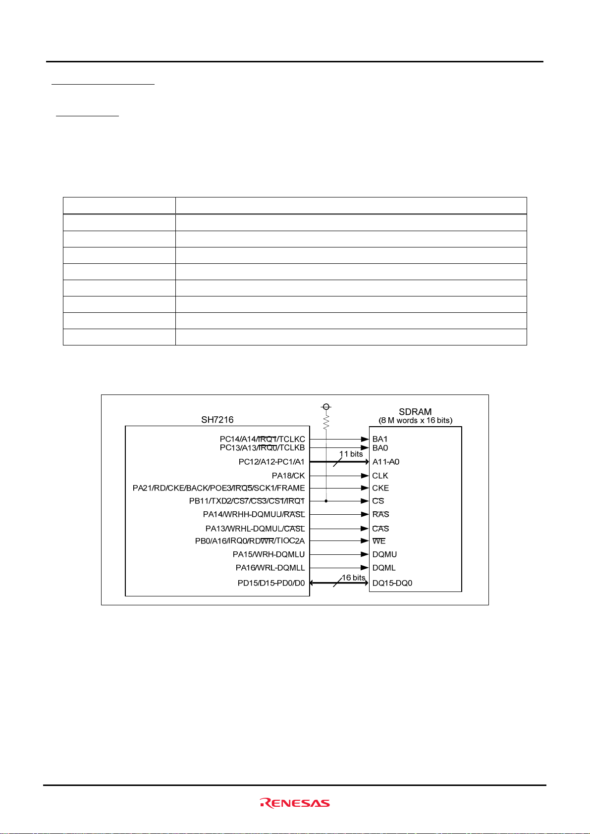
2.3 External Memory
2.3.1 SDRAM
The R0K572167 includes 16 MB of SDRAM. The SH7216 on-chip bus state controller (BSC) controls the SDRAM.
The following table lists the SDRAM specifications.
Table 2.3.1 SDRAM Specifications
Item Specification
Configuration 2 megawords x 16 bits x 4 banks
Capacity 16 MB (8 M words/16 bits)
Access time 5.4 ns
CAS latency 2 (when bus clock is 50 MHz)
Refresh interval 4096 cycles every 64 ms
Row address A11-A0
Column address A8-A0
Number of banks 4 (controlled by BA0 and BA1)
Functions
The following figure shows the SDRAM connection circuit for the SH7216 MCU and SDRAM.
Figure 2.3.1 Connection Circuit for the SH7216 and SDRAM
Rev. 0.02 Mar. 27, 2009 2-4
REJ11J0038-0002
Page 21
Functions
2
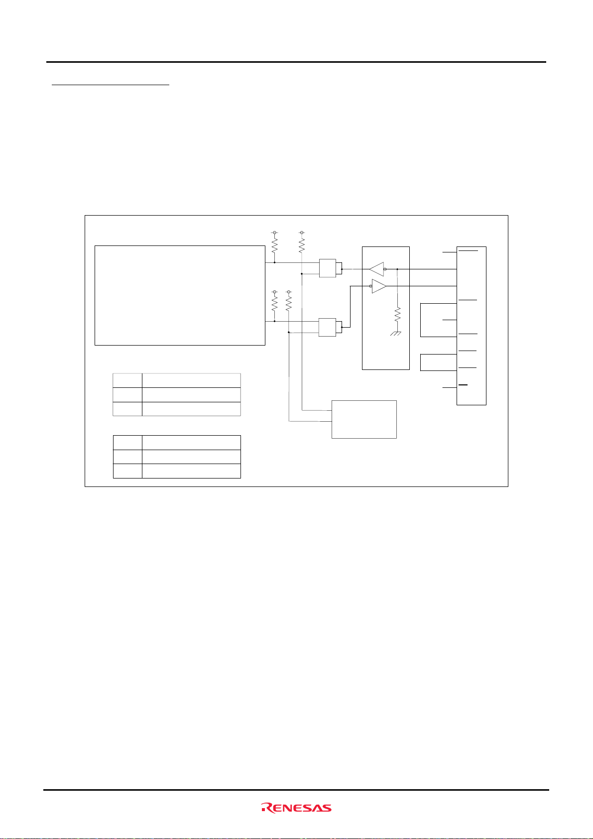
2.4 Serial Port Interface
2.4 Serial Port Interface
On the R0K572167, SH7216 SCI channel 1 is connected to the serial port connector via the RS-232C transceiver. Also,
SH7216 SCI channel 1 can be connected to the expansion connector (JA6), and the expansion connector can be
connected to the serial port connector via the RS-232C transceiver. When using SH7216 SCI channel 1 as a serial port,
do not connect it to the expansion connector.
The following figure shows the block diagram of the serial port on the R0K572167.
NC
GND
NC
Serial port
connector
1
DCD
2
RxD
3
TxD
4
DTR
5
GND
6
DSR
7
RTS
8
CTS
9
RI
SH7216
PA3/RXD1/MISO/CS3/TCLKC/MII_RXD2
PA4/TXD1/MOSI/CS4/TCLKB/MII_RXD3
JP2
1-2 TXD1 - RS232C
3-4 JA6 - RS232C
1-3 TXD1 - JA6
JP4
RS-232C
transceiver
JP4
2
1
3
4
JP2
2
1
3
4
Expansion connector (JA6)
RS232RX
RS232TX
1-2 RXD1 - RS232C
3-4 JA6 - RS232C
1-3 RXD1 - JA6
Figure 2.4.1 Serial Port Block Diagram
Rev. 0.02 Mar. 27, 2009 2-5
REJ11J0038-0002
Page 22
Functions
2
2.5 I/O Ports
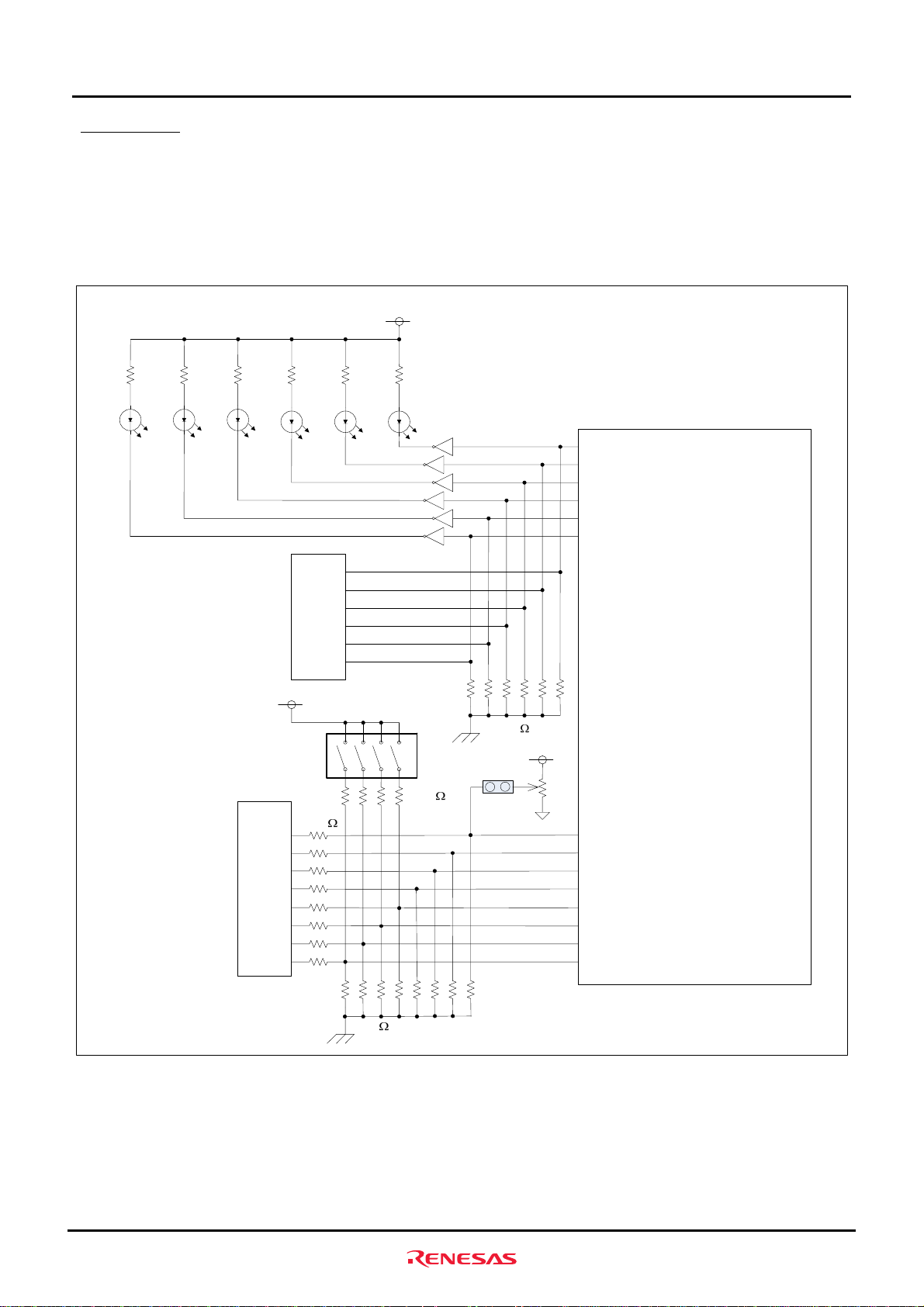
2.5 I/O Ports
SH7216 I/O ports are connected to the expansion connector on the R0K572167. Some I/O ports are also connected to
DIP switches and LEDs, and can be used at the user’s discretion.
The following figure shows the connection diagram of the LEDs and DIP switches.
5VCC
LED7
Green
LED6
Green
LED5
Green
User DIP switches
(SW5)
JA6
VccQ
LED4
Green
14
15
16
17
18
19
20
21
100
JA2
LED3
Green
13
14
15
16
17
18
SW3-4
LED2
Green
HD74LV06ATELL
PE9/TIOC3B/DACK2/TX_EN
PE11/TIOC3D/DACK3/MII_TXD0
PE12/TIOC4A/MII_TXD1
PE13/TIOC4B/MRES/MII_TXD2
PE14/DACK0/TIOC4C/MI_TXD3
PE15/DACK1/TIOC4D/IRQOUT/TX_ER
SW3-1
SW3-2
SW3-3
4.7 K
100 K
AVREF
VR1
JP10
PF0/AN0
PF1/AN2
PF2/AN2
PF3/AN3
PF4/AN4
PF5/AN5
PF6/AN6
PF7/AN7
SH7216
100 K
Figure 2.5.1 Connection Diagram of LEDs and DIP Switches
Rev. 0.02 Mar. 27, 2009 2-6
REJ11J0038-0002
Page 23
Functions
[23]
[7]
2
Table 2.5.1 and Table 2.5.2 list the I/O port functions.
Table 2.5.1 I/O Port Functions (1/2)
No. Pin name JA1 JA2 JA3 JA5 JA6
1 PE1/TIOC0B/TIOC4BS/TEND0/MDC 20 TIOC0B/TIOC4BS
2 PE2/TIOC0C/TIOC4CS/DREQ1/WOL 21 TIOC0C/TIOC4CS
3 PE3/TIOC0D/TIOC4DS/TEND1/COL 22 TIOC0D/TIOC4DS
4 PE4/TIOC1A/SCK3/POE8/IRQ4/CRS 12 TIOC1A/SCK3
5 PE5/TIOC1B/TIOC3BS/TXD3/MDIO 10 TIOC1B/TIOC3BS/TXD3
6 PE6/TIOC2A/TIOC3DS/RXD3 11 TIOC2A/TIOC3DS/RXD3
9 PA21/RD/CKE/BACK/POE3/IRQ5/SCK1/FRAME 46 CKE
10 PA20/WRL-DQMLL/CASU/BREQ/POE4/IRQ6/TXD1/AH
11 PA19/WRH-DQMLU/RASU/WAIT/POE8/IRQ7/RXD1/BS 15 PA19
12 PA18/CK 44 CK
14 PA17/RD 25 RD
15 PA16/WRL-DQMLL 48 WRL-DQMLL
16 PA15/WRH-DQMLU 47 WRH-DQMLU
17 PA14/WRHH-DQMUU/RASL 50 RASL
18 PA13/WRHL-DQMUL/CASL 49 CASL
21 PC0/A0/POE0/IRQ4 1 A0
22 PC1/A1 2A1
23 PC2/A2 3A2
24 PC3/A3 4A3
25 PC4/A4 5A4
26 PC5/A5 6A5
27 PC6/A6 7A6
28 PC7/A7 8A7
30 PC8/A8/CRx0/RXD0 9 A8
31 PC9/A9/CTx0/TXD0 10 A9
32 PC10/A10/TIOC1A/CRx0/RXD0 11 A10
33 PC11/A11/TIOC1B/CTx0/TXD0 12 A11
34 PC12/A12/TCLKA 13 A12
35 PC13/A13/IRQ0/TCLKB 14 A13
36 PC14/A14/IRQ1/TCLKC 15 A14
37 PC15/A15/IRQ2/TCLKD 16 A15
41 PB0/A16/IRQ0/RDWR/TIOC2A 37/26 A16/RDWR
42 PB1/A17/IRQOUT/ADTRG/TIOC0A/IRQ1 38 A17
43 PB2/A18/RASL/IRQ2/RXD3/TIOC0B/BACK/FRAME 39 A18
44 PB3/A19/CASL/IRQ3/TXD3/TIOC0C/BREQ/AH 40 A19
45 PB4/A20/IRQ4/SCK3/TIOC0D/WAIT/BACK/BS 41 A20
46 PB5/A21/IRQ5/RXD0/BREQ 42 A21
47 PB6/A22/IRQ6/TXD0/TCLKD/WAIT 43 A22
48 PB7/A23/IRQ7/SCK4/TCLKC/TEND0 3 TEND0
52 PB8/A24/CS2/TCLKB/DREQ0/RXD4 1 DREQ0
53 PB9/A25/CS3/TCLKA/DACK0/TXD4 2 DACK0
54 PB10/RXD2/CS6/CS2/CS0/IRQ0 27 CS2
55 PB11/TXD2/CS7/CS3/CS1/IRQ1 28 CS3
57 PD0/D0 17 D0
58 PD1/D1 18 D1
59 PD2/D2/TIC5U/RXD2 19 D2
60 PD3/D3/TIC5V/TXD2 20 D3
61 PD4/D4/TIC5W/SCK2 21 D4
62 PD5/D5/TIC5US 22 D5
63 PD6/D6/TIC5VS 23 D6
64 PD7/D7/TIC5WS 24 D7
67 PD8/D8/TIOC3AS 29 D8
68 PD9/D9/TIOC3CS 30 D9
69 PD10/D10/TIOC3BS 31 D10
70 PD11/D11/TIOC3DS 32 D11
71 PD12/D12/TIOC4AS 33 D12
72 PD13/D13/TIOC4BS 34 D13
73 PD14/D14/TIOC4CS 35 D14
74 PD15/D15/TIOC4DS 36
77 PD16/D16/IRQ0/POE0/UBCTRG/AUDATA0
78 PD17/D17/IRQ1/POE4/ADTRG/AUDATA1 13 ADTRG/AUDATA1
Brackets [] indicate the signals connected to the CPU pin via a device, element, and jumper.
SH7216 Expansion Connectors
IRQ6
D15
IRQ0/AUDATA0
2.5 I/O Ports
Remarks
Rev. 0.02 Mar. 27, 2009 2-7
REJ11J0038-0002
Page 24

Functions
[22]
_
[15]
[
_
[14]
[
_
[13]
[
_
[8]
_
[6]
_
[12]
[
_
[11]
[
_
[10]
[
_
[20]
[9]
[TX_ER][
]
(
[3]
[
[1]
[
_
_
_
_
[6] [
_
[5] [
_
_
_
_
_
_
_
_
_
2
Table 2.5.2 I/O Port Functions (2/2)
No. Pin name JA1 JA2 JA3 JA5 JA6
82
PD21/D21/IRQ5/TEND1/AUDCK/EXOUT
83
PD22/D22/IRQ6/DREQ1/WOL
93
PD30/D30/TIOC3CS/SSL3/RX
94
PD31/D31/TIOC3AS/SSL2/RX
97
PA12/IRQ0/TIC5U/CS0/SSL1/TX
98
PA11/IRQ1/TIC5V/CS1/TX
99
PA10/IRQ2/TIC5W/CS2/MII
100
PA9/IRQ3/TCLKD/CS3/MII
101
PA8/IRQ4/TCLKC/CS4/MII
102
PA7/IRQ5/TCLKB/CS5/MII
103
PA6/IRQ6/TCLKA/CS6/TX
110
PB12/SCL/POE1/IRQ2
111
PB13/SDA/POE2/IRQ3
116
PB14/IRQ6
117
121
123
133
138
139
140
141
146
147
148
149
154
157
158
159
160
161
162
165
166
167
168
169
170
171
172
173
176
PUPD)/IRQ7
PB15/
EXTAL
NMI
RES
PF0/AN0
PF1/AN1
PF2/AN2
PF3/AN3
PF4/AN4
PF5/AN5
PF6/AN6
PF7/AN7
WDTOVF
PA0/RXD0/CS0/CRx0/IRQ4/RX
PA1/TXD0/CS1/CTx0/IRQ5/MII
PA2/SCK0/SSL0/CS2/TCLKD/MII
PA3/RXD1/MISO/CS3/TCLKC/MII
PA4/TXD1/MOSI/CS4/TCLKB/MII
PA5/SCK1/RSPCK/CS5/TCLKA/RX
PE7/TIOC2B/UBCTRG/RXD2/SSL1/RX
PE8/TIOC3A/DREQ2/SCK2/SSL2/EXOUT
PE10/TIOC3C/DREQ3/TXD2/SSL3/TX
PE9/TIOC3B/DACK2/TX
PE11/TIOC3D/DACK3/MII
PE12/TIOC4A/MII
PE13/TIOC4B/MRES/MII
PE14/DACK0/TIOC4C/MI
PE15/DACK1/TIOC4D/IRQOUT/TX
PE0/TIOC0A/TIOC4AS/DREQ0/LINKSTA
Brackets [] indicate the signals connected to the CPU pin via device, element, and jumper.
.
SH7216 Expansion Connectors
21 WOL
ER
DV
CLK
EN/CRx0/RXD0
TXD0/CTx0/TXD0
TXD1/SSL0/SCK0
TXD2/MISO/RXD1
TXD3/MOSI/TXD1
ER/RSPCK/SCK1
CLK
RXD0
RXD1
RXD2
RXD3
ER
DV
CLK
EN
TXD0
TXD1
TXD2
TXD3
ER
25 SCL
26 SDA
17 PB14
16 PB15
2 EXTAL
5WDTOVF
12 TCLKD
11 TCLKA
13 PE9/TIOC3B
14 PE11/TIOC3D
15 PE12/TIOC4A
16 PE13/TIOC4B
17 PE14/TIOC4C
18 PE15/TIOC4D
19 TIOC0A/TIOC4AS
PDX21
SSL3]
SSL2]
SSL1]
SSL0]
MISO]
MOSI]
NMI]
RES]
14 AN0 [VR1]
15 AN1
16 AN2
17 AN3
18 PF4/AN4
19 PF5/AN5
20 PF6/AN6
21 PF7/AN7
6 CRx0
5CTx0
RXD1]
TXD1]
8 TIOC2B/RXD2
9 TIOC3A/SCK2
7 TIOC3C/TXD2
2.5 I/O Ports
Remarks
RSPCK
Rev. 0.02 Mar. 27, 2009 2-8
REJ11J0038-0002
Page 25

Functions
2
2.6 USB Interface
2.6 USB Interface
The R0K572167 includes a USB port connector (Series-B receptacle). Use the SH7216 PUPD output pin (PB15) to
control the USB line. Set the PUPD pin to a low level to disable the VBUS input and USD+ pull-up when delaying the
connection notification (such as high-priority processing or initialization) to a USB host or hub.
When the PUPD pin is set to a high level and VBUS power is supplied from the USB port connector, the SH7216 VBUS
input and USD+ pull-up are enabled, and the USB host or hub detects that a USB device has been connected.
When the VBUS pin is set to a low level, the SH7216 MCU retains its powered state regardless of the USD+ or USDstate.
When connecting a USB cable to a USB host or hub when this board is not ON, the USB host or hub supplies the
voltage to the VBUS. Be sure to turn the CPU board ON before connecting the USB cable.
The following figure shows the R0K572167 USB interface block diagram.
3.3 V
3.3 V
Ceramic resonator
(built-in capacitors)
CSTCZ48M0X11R
(Murata)
SH7216
DrVCC
DrVSS
USBEXTAL
USBXTAL
PB15/(PUPD)/IRQ7
Vbus PUPD VBUS D+ Remarks
0 0 0 Hi-Z Default value
0 1 0 Hi-Z
1 0 0 Hi-Z
1 1 1 Pull-up When USB is connected
VccQ
VBUS
USD+
USD-
PB14/IRQ6
HD74LV1GT08ACME-E
HD74LV1GT126ACME-E
3.3 V
3.3 V
47 K
JP1
Select the clock when
in USB boot mode
OE
3.3 V
USB Series-B
receptacle
Vbus
D+
D-
GND
Figure 2.6.1 USB Interface Block Diagram
Rev. 0.02 Mar. 27, 2009 2-9
REJ11J0038-0002
Page 26

Functions
2
2.7 RCAN Interface
2.7 RCAN Interface
The R0K572167 includes an RCAN port connector (D-sub, 9-pin connector). The CTx0 and RTx0 pins are connected to
the RCAN connector (J10) via the RCAN transceiver. These pins can be connected to the expansion connector (JA5)
via the switch jumpers (JP5 and JP6).
The following figure shows the R0K572167 RCAN interface block diagram.
U1
PA1/TXD0/CS1/CTx0/IRQ5/MII_RXD0
PA0/RXD0/CS0/CRx0/IRQ4/RX_CLK
SH7216
JP5
1
2
3
From JA5
JP6
1
2
3
To JA5
VccQ
VccQ
Voltage shifter IC
3.3/5 V to 5 V
U15
VccA
DIR
Voltage shifter IC
5 V to 3.3/5 V
VccQ
U17
VccA
A
DIR
→
GND
←
GND
VccB
5VCC
VccB
5VCCVccQ
BA
5VCC
B
Figure 2.7.1 RCAN Interface Block Diagram
RCAN transceiver IC
5VCC
U16
TxD
RxD CANH
CANL
RCAN connector
D-sub 9-pin
J10
CANH
CANL
Rev. 0.02 Mar. 27, 2009 2-10
REJ11J0038-0002
Page 27

2
2.8 Ethernet Interface
The R0K572167 includes an Ethernet port connector (RJ-45 connector) with a built-in pulse transformer.
The following figure shows the R0K572167 Ethernet interface block diagram.
Functions
2.8 Ethernet Interface
Figure 2.8.1 Ethernet Interface Block Diagram
Rev. 0.02 Mar. 27, 2009 2-1 1
REJ11J0038-0002
Page 28

2
2.9 Interrupt Switches
The SH7216 NMI and IRQ6 pins are connected to the push-button switches on the R0K572167.
The following figure shows the interrupt switch block diagram.
Functions
2.9 Interrupt Switches
Figure 2.9.1 Interrupt Switch Block Diagram
Rev. 0.02 Mar. 27, 2009 2-12
REJ11J0038-0002
Page 29

Functions
2
2.10 E10A-USB Interface
2.10 E10A-USB Interface
The R0K572167 includes two H-UDI port connectors (J1 and J2) to connect to the E10A-USB emulator.
The SH7216 ASEBRKAK
OFF to connect the R0K572167 to the E10A-USB emulator. If SW1-1 is ON, the R0K572167 cannot be debugged
correctly. Do not use the AUD pin when using the Ethernet interface.
The following figure shows the E10A-USB interface block diagram.
____________________
________________
/ASEBRK
/FEW pins are connected to the SW1-1 system setting DIP switch. Turn SW1-1
36-pin H-UDI port connector
2
GND
4
GND
6
GND
8
GND
10
GND
12
GND
14
GND
16
GND
18
GND
20
GND
22
(GND)
24
GND
26
GND
28
GND
ASEBRKAK
30
GND
32
GND
34
GND
36
GND
14-pin H-UDI port connector
9
(GND)
10
GND
12
GND
13
GND
ASEBRKAK/ASEBRK
14
GND
AUDCK
AUDSYNC
AUDATA3
AUDATA2
AUDATA1
AUDATA0
N.C.
N.C.
TCK
TMS
TRST
TDO
/ASEBRK
UVCC
RES
GND
N.C.
TRST
TMS
RES
N.C.
UVCC
TDI
TCK
TDO
TDI
VccQ
1
11
9
7
5
3
13
15
17
19
21
23
25
27
29
31
33
35
Turn OFF when using
1
2
3
4
5
6
7
8
11
the E10A-USB emulator
VccQ
SW1-1
VccQ
VccQ
Reset signal
VccQ
AUD/Ethernet, ADTRG, IRQ0
VccQ
SN74CBTLV16210
SH7216
PD21/D21/IRQ5/TEND1/AUDCK/EXOUT
PD20/D20/IRQ4/AUDSYNC
PD19/D19/IRQ3\/AUDATA3/LINKSTA
PD18/D18/IRQ2/AUDATA2/MDIO
PD17/D17/IRQ1/POE4/ADTRG/AUDATA1
PD16/D16/IRQ0/POE0/UBCTRG/AUDATA0
TCK
TMS
TRST
TDI
TDO
FWE/ASEBRKAK
ASEMD0
RES
MDC
LINKSTA
MDIO
ADTRG
IRQ0
EXOUT
/MDC
/ASEBRK
Ethernet
PHY
Figure 2.10.1 E10A-USB Interface Block Diagram
Rev. 0.02 Mar. 27, 2009 2-13
REJ11J0038-0002
Page 30

Functions
2
2.11 Power Supply Module
2.11 Power Supply Module
A 5 V power supply is input to R0K572167, and the regulator on the R0K572167 generates 1.5 V and 3.3 V. As it is a step
down DC-DC switching regulator, the desired voltage can be generated by changing the resistance value. The R0K572167
can use a 5 V DC output stabilized power supply via power connector J4 or J6. The R0K572167 can use the jumper setting to
supply external power supplies to the SH7216 system power (CVCC, 15 V), (3VCC, 3.3 V), A/D power supply (AVCC, 5 V),
and ACREF power supply (AVREF, 5 V).
The following figure shows the R0K572167 power supply circuit block diagram.
3VCC
Figure 2.11.1 Power Supply Circuit Block Diagram
Rev. 0.02 Mar. 27, 2009 2-14
REJ11J0038-0002
Page 31

Functions
R
2
2.12 Clock Module
2.12 Clock Module
The R0K572167 clock module is composed of two blocks. One block connects a crystal unit to EXTAL and XTAL, and
one block connects EXTAL to the expansion connector (JA2). As a default, a 12.5 MHz crystal unit is connected to
EXTAL and XTAL.
The following figure shows the clock module block diagram.
Figure 2.12.1 Clock Module Block Diagram
2.13 Reset Module
The reset module controls the reset signal of the SH7216.
The following figure shows the R0K572167 reset circuit block diagram.
+
RbRa
×
25.1
=
b
Figure 2.13.1 Reset Circuit Block Diagram
Rev. 0.02 Mar. 27, 2009 2-15
REJ11J0038-0002
Page 32

2
Functions
2.13 Reset Module
This page intentionally left blank.
Rev. 0.02 Mar. 27, 2009 2-16
REJ11J0038-0002
Page 33

Chapter 3Operating Specifications
Chapter 3
Operating Specifications
3-1
Page 34

3
3.1 Connectors
Figure 3.1.1 and Figure 3.1.2 show the connector assignments for the R0K572167.
Operating Specifications
3.1 Connectors
Figure 3.1.1 R0K572167 Connector Assignments (Top View of the Component Side)
Rev. 0.02 Mar. 27, 2009 3-2
REJ11J0038-0002
Page 35

3
Operating Specifications
3.1 Connectors
Figure 3.1.2 R0K572167 Connector Assignments (Top View of the Solder Side)
Rev. 0.02 Mar. 27, 2009 3-3
REJ11J0038-0002
Page 36

Operating Specifications
3
3.1.1 H-UDI Port Connectors (J2 and J3)
The R0K572167 includes 36-pin (J2) and 14-pin (J3) H-UDI port connectors to connect the board to an E10A-USB
emulator.
The following figure shows the pin assignments for J2.
3.1.1 H-UDI Port Connectors (J2 and J3)
Figure 3.1.3 J2 Pin Assignments
The following table lists the pin descriptions for J2.
Table 3.1.1 J2 Pin Descriptions
Pin Number Signal Name Pin Number Signal Name
1
2
3
4
5
6
7
8
9
10
11
12
13
14
15
16
17
18
AUDCK
GND
AUDATA0
GND
AUDATA1
GND
AUDATA2
GND
AUDATA3
GND
________________
AUDSYNC
GND
NC
GND
NC
GND
TCK
GND
19
20
21
22
23
24
25
26
27
28
29
30
31
32
33
34
35
36
TMS
GND
_________
TRST
ASEMD# (GND)
TDI
GND
TDO
GND
___________________
ASEBRKAK
GND
UVCC
GND
_______
RES
GND
GND
GND
NC
GND
______________
/ASEBRK
Rev. 0.02 Mar. 27, 2009 3-4
REJ11J0038-0002
Page 37

3
The following figure shows the pin assignments for J3.
Operating Specifications
3.1.1 H-UDI Port Connectors (J2 and J3)
714613512411310291
Top view of the
component side
8
J3
Side view
Note that the pin number assignments of this connector differ from those of
the connector manufacturer.
714613512411310291
13
11
7
9
5
3
8
1
Pin assignments
of this connector
Pin assignments
by connector
4
14 6
12
10
8
2
manufacturer
Figure 3.1.4 J3 Pin Assignments
The following table lists the pin descriptions for J3.
Table 3.1.2 J3 Pin Descriptions
Pin Number Signal Name Pin Number Signal Name
1
2
3
4
5
6
7
TCK
_________
TRST
TDO
___________________
ASEBRKAK
TMS
TDI
_______
RES
______________
/ASEBRK
8
9
10
11
12
13
14
NC
ASEMD# (GND)
GND
UVCC
GND
GND
GND
Rev. 0.02 Mar. 27, 2009 3-5
REJ11J0038-0002
Page 38

3
3.1.2 Serial Port Connector (J7)
The R0K572167 includes a serial port connector (J7).
The figure below shows the pin assignments for the serial port connector.
Operating Specifications
3.1.2 Serial Port Connector (J7)
Board edge
Board edge
The following table lists the pin descriptions for J7.
Pin Number Signal Name
1 NC
2 RXD
3 TXD
4 DTR
_______
5 GND
6 DSR
7 RTS
8 CTS
_______
_______
_______
9 NC
Pins 4 to 6, and 7 to 8 are loopback-connected.
1
6
1
6
5
9
5
9
Figure 3.1.5 J7 Pin Assignments
Table 3.1.3 J7 Pin Descriptions
Top view of the
component side
Side view
Rev. 0.02 Mar. 27, 2009 3-6
REJ11J0038-0002
Page 39

3
3.1.3 Power Supply Connector (J4)
The R0K572167 includes a power supply connector (J4).
The following figure shows the pin assignments for J4.
12
Board edge
12
Board edge
Operating Specifications
3.1.3 Power Supply Connector (J4)
Top view of the
component side
Side view
Figure 3.1.6 J4 Pin Assignments
The following table lists the pin descriptions for J4.
Table 3.1.4 J4 Pin Descriptions
Pin Number Signal Name
1 +5 V
2 GND
Rev. 0.02 Mar. 27, 2009 3-7
REJ11J0038-0002
Page 40

Operating Specifications
3
3.1.4 SH7216 External Power Supply Connectors (J8, J9, J12, J13)
External power supply connectors for CPU power, USB power, and analog power can be mounted on the R0K572167.
To supply power using these connectors, remove the receptacle of the external power supply jumpers (JP8, JP9,
JP12, and JP13) to leave it open.
The following figure shows the pin assignments for the external power supply connectors.
3.1.4 SH7216 External Power Supply Connectors (J8, J9, J12, J13)
Figure 3.1.7 External Power Supply Connector Pin Assignments
J13 is a connector for supplying the CPU core voltage externally. As the SH7216 generates the core voltage from a 3.3 V
power supply inside the LSI, J13 is not used on the R0K572167.
Rev. 0.02 Mar. 27, 2009 3-8
REJ11J0038-0002
Page 41

3
The following table lists the pin descriptions for J13.
Table 3.1.5 J13 Pin Descriptions
Pin Number Signal Name
1 CVCC
2 GND
The following table lists the pin descriptions for J12.
Table 3.1.6 J12 Pin Descriptions
Pin Number Signal Name
1 3VCC
2 GND
The following table lists the pin descriptions for J9.
Table 3.1.7 J9 Pin Descriptions
Pin Number Signal Name
3.1.4 SH7216 External Power Supply Connectors (J8, J9, J12, J13)
Operating Specifications
1 AVREF
2 AVREFVSS
The following table lists the pin descriptions for J8.
Table 3.1.8 J8 Pin Descriptions
Pin Number Signal Name
1 AVCC
2 AGND
Rev. 0.02 Mar. 27, 2009 3-9
REJ11J0038-0002
Page 42

3
3.1.5 DC Power Supply Jack (J6)
The R0K572167 includes a DC power supply jack (J6).
The following figure shows the pin assignments for J6.
Operating Specifications
3.1.5 DC Power Supply Jack (J6)
J6
Figure 3.1.8 J6 Pin Assignments
The table below lists the pin descriptions for J6.
Table 3.1.9 J6 Pin Descriptions
Pin Number Signal Name
1
2
3
GND
GND
+5 V
Rev. 0.02 Mar. 27, 2009 3-10
REJ11J0038-0002
Page 43

Operating Specifications
3
3.1.6 Expansion Connectors (JA1, JA2, JA3, JA5, JA6)
The R0K572167 includes through-holes for mounting expansion connectors. The SH7216 I/O pins are connected to
the through-holes. The standard MIL connector can be connected to the through-holes to connect the expansion
board, and to monitor the SH7216 bus signals.
Figure 3.1.9 and Figure 3.1.10 show the pin assignments for the expansion connectors.
3.1.6 Expansion Connectors (JA1, JA2, JA3, JA5, JA6)
23
24
23
24
JA6
1225
1225
1
26
26
JA1JA5
JA2
2
50
49
JA3
2
1
1
2
Figure 3.1.9 Expansion Connectors Pin Assignments (Top View of the Component Side)
Rev. 0.02 Mar. 27, 2009 3-11
REJ11J0038-0002
Page 44

3
Operating Specifications
3.1.6 Expansion Connectors (JA1, JA2, JA3, JA5, JA6)
JA3
1
2
50
49
2
1
1
2
JA1 JA5
JA2
25
2612
25
2612
23
24
JA6
23
24
Figure 3.1.10 Expansion Connectors Pin Assignments (Top View of the Solder Side)
Note: Pin assignments on the CPU board are based on the assumption that the expansion connectors are mounted
on the component side. If the expansion connectors are mounted on the solder side, these pin assignments do
not apply.
Rev. 0.02 Mar. 27, 2009 3-12
REJ11J0038-0002
Page 45

3
The following table lists the pin descriptions for JA1.
Table 3.1.10 JA1 Pin Descriptions
Pin Number
1 5VCC ―
2 GND ―
3 3VCC ―
4 GND ―
5 AVCC ―
6 AGND ―
7 AVREF ―
8 ― ―
9 ― ―
10 ― ―
11 ― ―
12 ― ―
13 ― ―
14 ― ―
15 PA19/WRH-DQMLU/RASU/WAIT/POE8/IRQ7/RXD1/BS ―
16 PB15/(PUPD)/IRQ7 U10-1 (VBUS voltage detect control)
17 PB14/IRQ6 ―
18 ― ―
19 ― ―
20 TX_ER ―
21 PD22/D22/IRQ6/DREQ1/WOL ―
22 PDX21 ―
23
24 ― ―
25 PB13/SDA ―
26 PB12/SCL ―
IRQ6IN
Signal Name
Operating Specifications
3.1.6 Expansion Connectors (JA1, JA2, JA3, JA5, JA6)
Other Connections
―
Rev. 0.02 Mar. 27, 2009 3-13
REJ11J0038-0002
Page 46

3
The following table lists the pin descriptions for JA2.
Table 3.1.11 JA2 Pin Descriptions
Pin Number Signal Name
1 RESET# ―
2 EXTAL ―
3 NMIIN ―
4 GND ―
5 WDTOVF# ―
6 TXD0 ―
7 IRQ0 ―
8 RXD0 ―
9 ― ―
10 ― ―
11 PA5/SCK1/RSPCK/CS5/TCLKA/RX_ER ―
12 PA2/SCK0/SSL0/CS2/TCLKD/MII_RXD1 ―
13 PE9/TIOC3B ―
14 PE11/TIOC3D ―
15 PE12/TIOC4A ―
16 PE13/TIOC4B ―
17 PE14/TIOC4C ―
18 PE15/TIOC4D ―
19 PE0/TIOC0A/TIOC4AS/DREQ0/LINKSTA ―
20 PE1/TIOC0B/TIOC4BS/TEND0/MDC ―
21
22
23
24
25
.
PE2/TIOC0C/TIOC4CS/DREQ1/WOL ―
PE3/TIOC0D/TIOC4DS/TEND1/COL ―
― ―
― ―
― ―
Operating Specifications
3.1.6 Expansion Connectors (JA1, JA2, JA3, JA5, JA6)
Other Connections
Rev. 0.02 Mar. 27, 2009 3-14
REJ11J0038-0002
Page 47

3
The following table lists the pin descriptions for JA3.
Table 3.1.12 JA3 Pin Descriptions
Pin Number Signal Name Other Connections
1
2
3
4
5
6
7
8
9
10
11
12
13
14
15
16
17
18
19
20
21
22
23
24
25
26
27
28
29
30
31
32
33
34
35
36
37
38
39
40
41
42
43
44
45
46
47
48
49
50
A0 ―
A1
A2
A3
A4
A5
A6
A7
A8
A9
A10
A11
A12
A13
A14
A15
D0
D1
D2
D3
D4
D5
D6
D7
RD
RDWR
CS2
CS3
D8
D9
D10
D11
D12
D13
D14
D15
A16
A17
A18
A19
A20
A21
A22
CK
―
CKE
WRH/DQMLU
WRL/DQMLL
CAS
RAS
3.1.6 Expansion Connectors (JA1, JA2, JA3, JA5, JA6)
SDRAM
SDRAM
SDRAM
SDRAM
SDRAM
SDRAM
SDRAM
SDRAM
SDRAM
SDRAM
SDRAM
SDRAM
SDRAM
SDRAM
―
SDRAM
SDRAM
SDRAM
SDRAM
SDRAM
SDRAM
SDRAM
SDRAM
―
SDRAM
―
SDRAM
SDRAM
SDRAM
SDRAM
SDRAM
SDRAM
SDRAM
SDRAM
SDRAM
RDWR
―
―
―
―
―
―
SDRAM
―
SDRAM
SDRAM
SDRAM
SDRAM
SDRAM
Operating Specifications
Rev. 0.02 Mar. 27, 2009 3-15
REJ11J0038-0002
Page 48

3
The following table lists the pin descriptions for JA5.
Table 3.1.13 JA5 Pin Descriptions
Pin Number Signal Name Other Connections
1 ― ―
2 ― ―
3 ― ―
4 ― ―
5 CTx0 U15-3 to RCAN transceiver
6 CRx0 U17-3 to RCAN transceiver
7 ― ―
8 ― ―
9 RSPCK ―
10 MOSI ―
11 M I S O ―
12 SSL0 ―
13 SSL1 ―
14 SSL2 ―
15 SSL3 ―
16 ― ―
17 ― ―
18 ― ―
19 ― ―
20 ― ―
21 ― ―
22 ― ―
23 ― ―
24 ― ―
3.1.6 Expansion Connectors (JA1, JA2, JA3, JA5, JA6)
Operating Specifications
Rev. 0.02 Mar. 27, 2009 3-16
REJ11J0038-0002
Page 49

3
The following table lists the pin descriptions for JA6.
Table 3.1.14 JA6 Pin Descriptions
Pin Number Signal Name Other Connections
1
2
3
4
5
6
7
8
9
10
11
12
13
14
15
16
17
18
19
20
21
22
23
24
DREQ0 ―
DACK ―
TEND ―
― ―
RS232TX ―
RS232RX ―
TXD2 ―
RXD2 ―
SCK2 ―
TXD3 ―
RXD3 ―
SCK3 ―
ADTRG ―
AD0 VR1 (potentiometer)
AD1 ―
AD2 ―
AD3 ―
AD4
AD5
AD6
AD7
AGND
―
GND
3.1.6 Expansion Connectors (JA1, JA2, JA3, JA5, JA6)
SW5-1
SW5-2
SW5-3
SW5-4
―
―
―
Operating Specifications
Rev. 0.02 Mar. 27, 2009 3-17
REJ11J0038-0002
Page 50

3
3.1.7 RCAN Port Connector (J10)
The R0K572167 supports RCAN transmission and reception.
The following figure shows the pin assignments for J10.
Operating Specifications
3.1.7 RCAN Port Connector (J10)
Figure 3.1.11 J10 Pin Assignments
The following table lists the pin descriptions for J10.
Table 3.1.15 J10 Pin Descriptions
Pin Number Signal Name
1
2
3
4
5
6
7
8
9
NC
CANL (U16)
GND
NC
NC
NC
CANH (U16)
NC
NC
Rev. 0.02 Mar. 27, 2009 3-18
REJ11J0038-0002
Page 51

3
3.1.8 USB Port Connector (J5)
The R0K572167 includes a USB port connector (Series-B receptacle).
The following figure shows the pin assignments for J5.
Operating Specifications
3.1.8 USB Port Connector (J5)
Top view of the
component side
Board edge
Side view
Board edge
The following table lists the pin descriptions for J5.
Pin Number Signal Name
1
2
3
4
Vbus
D-
D+
GND
2
3
2
Figure 3.1.12 J5 Pin Assignments
Table 3.1.16 J5 Pin Descriptions
1
4
1
43
Rev. 0.02 Mar. 27, 2009 3-19
REJ11J0038-0002
Page 52

3
3.1.9 LAN Port Connector (J1)
The R0K572167 includes a LAN port connector (J1).
The following figure shows the pin assignment for J1.
Operating Specifications
3.1.9 LAN Port Connector (J1)
Figure 3.1.13 J1 Pin Assignment
The following table lists the pin descriptions for J1.
Table 3.1.17 J1 Pin Descriptions
Pin Number Signal Name
1 TD+
2 TD-
3 TCT
4 RD+
5 RD-
6 RCT
7 NC
8 NC
Rev. 0.02 Mar. 27, 2009 3-20
REJ11J0038-0002
Page 53

3
3.1.10 GND Connector (J11)
The R0K572167 includes the GND connector (J11).
The following figure shows the pin assignments for J11.
Operating Specifications
3.1.10 GND Connector (J11)
JA3
Figure 3.1.14 J11 Pin Assignments
The following table lists the pin descriptions for J11.
Table 3.1.18 J11 Pin Descriptions
Pin Number Signal Name
1
2
3
GND
GND
GND
GNDJ11
13
Board edge
Rev. 0.02 Mar. 27, 2009 3-21
REJ11J0038-0002
Page 54

Operating Specifications
3
3.2 Switches and LEDs
3.2 Switches and LEDs
The R0K572167 includes switches, a potentiometer, and LEDs as operating components. For potentiometer accuracy,
refer to the manual provided by the manufacturer.
The following figure shows the assignments of the R0K572167 operating components.
SW2
PHY-LSI setting
DIP switches
LED1 to LED5
PHY-LSI LEDs
NMI switch
SW7
IRQ6 switch
SW6
Reset switch
LED6
Power supply LED
SW3
SW4
Power supply
switch
Analog input potentiometer
VR1
SW5
User DIP switches
SW1
System setting
DIP switches
LED7 to LED12
User LEDs
Figure 3.2.1 R0K572167 Operating Component Assignments (Top View of the Component Side)
Rev. 0.02 Mar. 27, 2009 3-22
REJ11J0038-0002
Page 55

Operating Specifications
3
3.2.1 USB Boot Clock Switch Jumper (JP1)
Set JP1 to switch the clock source in USB boot mode to the USB clock or system clock. Be sure to set the system
clock to 12 MHz when selecting the system clock.
The following figure shows the assignments of JP1.
JP1
3.2.1 USB Boot Clock Switch Jumper (JP1)
Figure 3.2.2 JP1 Assignments
The following table lists JP1 setting.
Table 3.2.1 JP1 Setting
Number Setting Description
JP1
Note: Do not change the jumper settings while the R0K572167 is ON. Be sure to turn the power OFF before changing
the settings.
1-2
2-3
Uses the system clock as the USB boot clock
Uses the USB clock as the USB boot clock (default setting)
Rev. 0.02 Mar. 27, 2009 3-23
REJ11J0038-0002
Page 56

Operating Specifications
3
3.2.2 External Power Supply Switch Jumpers (JP7, JP3, JP8, JP9)
Set JP3, JP8, and JP9 to switch the source of the power supply voltage to the system power supply (3VCC), analog
power supply (AVCC), and A/D reference power supply (AVREF). As the SH7216 MCU does not use JP7, it is not
mounted on this board.
The following figure shows the assignments of the external power supply switch jumpers.
Top view of the
component side
3.2.2 External Power Supply Switch Jumpers (JP7, JP3, JP8, JP9)
Board edge
FIX AVCC
AVCC SEL
AVREF SEL
3VCC SEL
1.5VCC SEL
2
FIX AVREF
2
FIX 3VCC
FIX 1.5VCC
Figure 3.2.3 External Power Switch Jumpers Assignments
The following table lists the external power supply switch jumpers setting.
Table 3.2.2 External Power Switch Jumper Setting
Number Setting Description
3VCC SEL
1-2
Open Uses the external power supply voltage (JA1 or J12)
Supplies the SH7216 USB power supply (3VCC) from J4 or J6 (via the regulator)
1-2 Connects the SH7216 AVCC to the 5 V fixed power supply voltage
AVCCSEL
AVREFSEL
Open Uses the external power supply voltage (JA1, J8, or H18)
1-2
Connects the SH7216 AVREF to the 5 V fixed power supply voltage
Open Uses the external power supply voltage (JA1, J9, or H19)
Notes:
1. Default setting.
2. Do not change the jumper settings while the board is ON. Be sure to turn the power OFF before changing
the settings.
2
JP8
1
JP9
1
JP3
12
JP7
12
J8
1
2
J9
1
2
J12
1
2
J13
1
(1)
JP3
(1)
JP8
(1)
JP9
Rev. 0.02 Mar. 27, 2009 3-24
REJ11J0038-0002
Page 57

Operating Specifications
3
3.2.3 Serial Port Switch Jumpers (JP2 and JP4)
Set the serial port switch jumpers (JP2 and JP4) to change the destination connector of the RS-232C transceiver,
which is connected to the serial power connector (J7).
SCI channel 1 is connected to J7 as default.
When connecting the RS232TX/RS232RX pins of JA6 to the RS-232C transceiver, do not use SCI channel 1.
SCI channel 1 can be connected directly to the RS232TX/RS232RX pins of JA6.
The following figure shows the assignments of JP2 and JP4.
Top view of the
component side
JP2
2
1
1
TXD
43
SEL
JP4
2
RXD
43
SEL
3.2.3 Serial Port Switch Jumpers (JP2 and JP4)
J10
Board edge
Figure 3.2.4 JP2 and JP4 Assignments
The following table lists JP2 and JP4 settings.
Table 3.2.3 JP2 and JP4 Settings
Number Setting Description
(1)
JP2
TXDSEL
1-2 Connects the SH7216 PA4/TXD1 pin to the RS-232C transceiver (U14)
3-4 Connects the RS232TX pin of JA6 to U14
1-3 Connects the SH7216 PA4/TXD1 pin to the RS232TX pin of JA6
1-2 Connects the SH7216 PA3/RXD1 pin to U14
(1)
JP4
RXD SEL
3-4 Connects the RS232RX pin of JA6 to U14
1-3 Connects the SH7216 PA3/RXD1 pin to the RS232RX pin of JA6
Notes:
1. Default setting.
2. Do not change the jumper settings while the board is ON. Be sure to turn the power OFF before changing the
settings.
Rev. 0.02 Mar. 27, 2009 3-25
REJ11J0038-0002
Page 58

Operating Specifications
3
3.2.4 RCAN Port Switch Jumpers (JP5 and JP6)
Set the RCAN port switch jumpers (JP5, and JP6) to switch the SH7216 pins connected to the RCAN transceiver (U16).
U16 is connected to the SH7216 PA1/CTx0 and PA0/CRx0 pins via the level shifter as default.
When not using these pins via U16, set JP5 and JP6 to 2-3.
The following figure shows the assignments of JP5 and JP6.
3.2.4 RCAN Port Switch Jumpers (JP5 and JP6)
Figure 3.2.5 JP5 and JP6 Assignments
The following table lists JP5 and JP6 settings.
Table 3.2.4 JP5 and JP6 Settings
Number Setting Description
1-2
TXDSEL
RXD SEL
Notes:
1. Default setting.
2. Do not change the jumper settings while the board is ON. Be sure to turn the power OFF before changing the
settings.
Open Connects the SH7216 PA1/CTx0 pin to JA5
1-2 Connects the SH7216 PA0/CRx0 pin to U16
Open Connects the SH7216 PA0/CRx0 pin to JA5
Connects the SH7216 PA1/CTx0 pin to U16
(1)
(1)
JP9
JP10
Rev. 0.02 Mar. 27, 2009 3-26
REJ11J0038-0002
Page 59

Operating Specifications
3
3.2.5 Switches and LEDs
The R0K572167 includes seven switches and 12 LEDs.
The following table lists the switches mounted on the board.
Table 3.2.5 Switches
No. Function Remarks
SW1 System setting DIP switches (4/package) Refer to Table 3.2.6 for functions.
SW2 PHY-LSI setting DIP switches (6/package)
SW2-1 ISOLATE
SW2-2 RPTR
SW2-3 SPEED
SW2-4 DUPLEX
SW2-5 ANE
SW2-6 LDPS
SW3 Reset switch Refer to Section 2.13 for details
SW4 Power supply switch ―
SW5 User DIP switches (4/package)
SW5-1 OFF: PE0 = high, ON: PE0 = low
SW5-2 OFF: PE1 = high, ON: PE1 = low
SW5-3 OFF: PE2 = high, ON: PE2 = low
SW5-4 OFF: PE3 = high, ON: PE3 = low
SW6 NMI switch Refer to Section 2.9 for details.
SW7 IRQ6 switch Refer to Section 2.9 for details.
Pins are pulled up.
Pins PF0, PF1, PF2, and PF3 are pulled down.
Refer to Section 2.5 for details.
3.2.5 Switches and LEDs
Rev. 0.02 Mar. 27, 2009 3-27
REJ11J0038-0002
Page 60

3
Operating Specifications
3.2.5 Switches and LEDs
The following table lists the SW1 functions. Set the SH7216 operating mode using the FWE, MD0, and MD1 pins.
The FWE pin is multiplexed to the ASEBRK
_______________
___________________
/ASEBRKAK
signals. Turn OFF SW1-1 (FWE) before using the
E10A-USB emulator.
Table 3.2.6 Switch (SW1) Functions
No. Setting Description
(1)
SW1-1
Operating mode setting
Signal line switch
FWE
MD1
MD0
Ethernet mode
OFF FWE is high (on-chip flash memory is write/erase enabled)
ON FWE is low (on-chip flash memory is write/erase protected)
OFF MD1 pin is fixed high
ON MD1 pin is fixed low
OFF MD0 pin is fixed high SW1-3
ON MD0 pin is fixed low
OFF AUD/RSPI/TXD0/RXD0 pins are enabled SW1-4
ON Ethernet/IRQ0/ADTRIG pins are enabled
(1)
SW1-2
(1)
(1)
Notes:
1. Default setting.
2. Do not change SW1 settings while the board is ON. Be sure to turn the power OFF before changing the
settings.
The following table lists the SH7216 operating mode setting.
Table 3.2.7 SH7216 Operating Mode Settings
SW1-1
(FWE)
ON ON ON Mode 0 MCU extension mode 0 (on-chip ROM is disabled, CS0 space: 32-bit bus)
ON ON OFF Mode 1 MCU extension mode 1 (on-chip ROM is disabled,CS0 space:16-bit bus)
ON OFF ON Mode 2 MCU extension mode 2 (on-chip ROM is enabled)
ON OFF OFF Mode 3 Single-chip mode (on-chip ROM enabled)
OFF ON ON Mode 4
OFF ON OFF Mode 5
OFF OFF ON Mode 6
OFF OFF OFF Mode 7
SW1-2
(MD1)
SW1-3
(MD0)
No. Name
(1)
Boot mode (on-chip ROM enabled)
(1)
User boot mode (on-chip ROM enabled)
(1)
User program mode (on-chip ROM enabled) (default setting)
(1)
USB boot mode (on-chip ROM enabled)
SH7216 Operating Mode
Notes:
1. Programming mode for the flash memory.
2. Do not change SW1 settings while the board is ON. Be sure to turn the power OFF before changing the
settings.
Rev. 0.02 Mar. 27, 2009 3-28
REJ11J0038-0002
Page 61

Operating Specifications
3
The following table lists the PHY operating mode settings.
Table 3.2.8 PHY Operating Mode Setting
No. Setting Description
OFF ISOLATE is high SW2-1
ISOLATE
RPTR
SPEED
DUPLEX
ANE
LDPS
Notes:
1. Default setting.
2. Do not change SW2 settings while the board is ON. Be sure to turn the power OFF before changing the
settings.
The following table lists the LEDs.
ON ISOLATE is low
OFF RPTR is high SW2-2
ON RPTR is low
OFF SPEED is high
ON SPEED is low
OFF DUPLEX is high
ON DUPLEX is low
OFF ANE is high
ON ANE is low
OFF LDPS is high SW2-6
ON LDPS is low
(1)
(1)
(1)
SW2-3
(1)
SW2-4
(1)
SW2-5
(1)
3.2.5 Switches and LEDs
PHY mode setting
Table 3.2.9 LEDs
Number Color Description/Remarks
LED1 Yellow PHY-LSI LED (LED_A)
LED2 Yellow PHY-LSI LED (LED_B)
LED3 Yellow PHY-LSI LED (LED_C)
LED4 Yellow PHY-LSI LED (LED_D)
LED5 Yellow PHY-LSI LED (LED_E)
LED6 Blue Power supply LED (LED6 is illuminated when power is supplied)
LED7 Green User LED (LED 7 is illuminated when PE9 outputs a high-level signal)
LED8 Green User LED (LED 8 is illuminated when PE11 outputs a high-level signal)
LED9 Green User LED (LED 9 is illuminated when PE12 outputs a high-level signal)
LED10 Green User LED (LED 10 is illuminated when PE13 outputs a high-level signal)
LED11 Green User LED (LED 11 is illuminated when PE14 outputs a high-level signal)
LED12 Green User LED (LED 12 is illuminated when PE15 outputs a high-level signal)
Rev. 0.02 Mar. 27, 2009 3-29
REJ11J0038-0002
Page 62

3
3.2.6 Jumper/Switch Setting when Using the Development Tools
3.2.6 Jumper/Switch Setting when Using the Development Tools
Operating Specifications
As the SH7216 signals connected to the emulator (FWE/ASEBRKAK
on-chip flash writing control pins, set the jumpers and switches as shown in the following table when using
development tools such as the E10A-USB emulator or the Flash Development Toolkit (FDT).
Table 3.2.10 Jumper/Switch Setting
Development Tool Connector
14-pin E10A-USB J3
36-pin E10A-USB J2
J7 OFF ON ON -
FDT
J5 OFF OFF OFF -
Note:
1: Do not change SW1 settings while the board is ON. Be sure to turn the power OFF before changing the settings
SW1-1 SW1-2 SW1-3 SW1-4
OFF OFF ON OFF RSPI can be used.
OFF OFF ON ON Ethernet can be used.
OFF OFF ON OFF RSPI and AUD can be used.
OFF OFF ON ON
_____________________
(1)
Setting
________________
/ASEBRK
, TDI, TDO pins) are multiplexed to the
Remarks
Ethernet can be used.
AUD cannot be used.
Mode 4
Boot mode
Mode 7
USB boot mode
Rev. 0.02 Mar. 27, 2009 3-30
REJ11J0038-0002
Page 63

3
3.3 Dimensions
Figure 3.3.1 and Figure 3.3.2 show the CPU board dimensions.
Operating Specifications
3.3 Dimensions
Figure 3.3.1 CPU Board Dimensions (Top View of the Component Side)
Rev. 0.02 Mar. 27, 2009 3-31
REJ11J0038-0002
Page 64

3
Operating Specifications
3.3 Dimensions
Figure 3.3.2 CPU Board Dimensions (Transparent View of the Solder Side)
Rev. 0.02 Mar. 27, 2009 3-32
REJ11J0038-0002
Page 65

3
Operating Specifications
3.3 Dimensions
This page intentionally left blank.
Rev. 0.02 Mar. 27, 2009 3-33
REJ11J0038-0002
Page 66

Appendix
SCHEMATICS
A-1
Page 67

1
2
3
4
5
SH7216 CPU Board R0K572167 SCHEMATICS
A A
Note:
TITLE
INDEX
SH7216
SDRAM-Ether/AUD,H-UDI,Reset
USB/SERIAL/RCAN/Power
B B
C C
Connectors,PUSH/DIP_SW,LED
PAGE
1
2
3
4
5
5VCC = Digital 5V
3VCC = 3.3V
1.5VCC = Core Vcc
AVCC = CPU Analog 5V
AVREF = CPU Analog 5V Reference
VccQ = CPU/etc. 3.3V
3AVCC = Ether Analog 3.3V
DrVCC = USB 3.3V
3VCC_SDRAM = SDRAM 3.3V
PLLVCC = CPU PLL 3.3V
CVCC = CPU Core 1.5V
R = Fixed Resistors
RA = Resister Array
C = Ceramic Caps
CE = Electrolytic Caps
CP = Decoupling Caps
(Put one cap
per each source pin)
CQ = Demitasse resonance Caps
L = Inductor
:not mounted
D D
Ver. 0.12
CHANGE
CHANGE
CHANGE
R98, R224 Remove
SCALE
SCALE
SCALE
DATE
DATE
DATE
09-03-25
09-03-25
09-03-25
1
2
3
RENESAS SOLUTIONS CORPORATION
RENESAS SOLUTIONS CORPORATION
RENESAS SOLUTIONS CORPORATION
APPROVED
APPROVED
DESIGNEDCHECKEDDRAWN
DESIGNEDCHECKEDDRAWN
DESIGNEDCHECKEDDRAWN
4
APPROVED
R0K572167
R0K572167
R0K572167
INDEX
INDEX
INDEX
DK30800
5
(
/)
15
(
/)
15
(
/)
15
Page 68

5
Mode Switch 1-3
Ether Mode Switch 4
DSW Power Switch 5
CP22
CP22
0.1µFP
0.1µFP
ON
OFF
ON
OFF
R8
4.7KΩR84.7KΩ
FWE
MD1
MD0
Ether_Mode
Ether Mode
Ether Mode
AUD Mode
DSW Power
Pull Up
Open
VccQ
R10
R10
4.7KΩ
4.7KΩ
R11 _0ΩR11 _0Ω
U2C
U2C
3 5
HD74LV2G14A
HD74LV2G14A
VccQ
84
U2D
U2D
HD74LV2G14A
HD74LV2G14A
CP23
CP23
0.1µFP
0.1µFP
ASEBRKAK#/ASEBRK#[3]
R120ΩR12
0Ω
C2
8pFC28pF
FWE
MD1
MD0
Ether_Mode [3]
R15 1MΩR15 1MΩ
CX5032GB 12500
CX5032GB 12500
X1
X1
1 3
VccQ
U3C
U3C
2 5
HD74LV1GW07A
HD74LV1GW07A
R250ΩR25
0Ω
R27 1MΩR27 1MΩ
X2
X2
3 1
2
R13
R13
560Ω
560Ω
R260ΩR26
0Ω
CSTCZ48M0X11R**-B0
CSTCZ48M0X11R**-B0
MODE
FWE MD1 MD0
0
LLL
1
L
L
8
7
6
5
H
H
L
L
H
SW1
SW1
ON
ON
A6S-4104
A6S-4104
R9
_4.7KΩR9_4.7KΩ
EXTAL[5]
H
L
H
L
H
L
1
2
3
4
2
L
3
D D
L
4
H
5
H
6
H
7
HHH
[12.5MHz:CPU]XTAL Type
C C
B B
[48MHz:USB]CERALOCK Type
4
AVCC
0.1µFP
0.1µFP
CP18
CP18
1 7
U3B
U3B
AVREF
0.1µFP
0.1µFP
CP21
CP21
FWE/ASEBRKAK#/ASEBRK#
R14
R14
560Ω
560Ω
0.01µFC10.01µF
43
HD74LV1GW07A
HD74LV1GW07A
VccQ
HD74LV1GW07A
HD74LV1GW07A
VccQ
JP1
JP1
1
3
XG8S-0331
XG8S-0331
CP24
CP24
0.001µFP
0.001µFP
CP27
CP27
0.001µFP
0.001µFP
0.1µFP
0.1µFP
CP20
CP20
U2B HD74LV2G14AU2B HD74LV2G14A
6 2
C1
RESET# [3,5]RESETSIG[3]
U3A
U3A
6 1
USB_XOUT
USB_XIN
2
CP25
CP25
0.01µFP
0.01µFP
CP28
CP28
0.01µFP
0.01µFP
AVREF[4,5]
AVREFVSS[4,5]
PF0/AN0[5]
PF1/AN1[5]
PF2/AN2[5]
PF3/AN3[5]
PF4/AN4[5]
PF5/AN5[5]
PF6/AN6[5]
PF7/AN7[5]
U2A HD74LV2G14AU2A HD74LV2G14A
C3
8pFC38pF
USB
LED
IIC
NMI[5]
WDTOVF#[5]
PA20/IRQ6[5]
PE9/TIOC3B[5]
PE11/TIOC3D[5]
PE12/TIOC4A[5]
PE13/TIOC4B[5]
PE14/TIOC4C[5]
PE15/TIOC4D[5]
PB12/SCL[5]
PB13/SDA[5]
PB14/IRQ6[5]
VBUS[4]
DP[4]
DM[4]
PB15/(PUPD)/IRQ7[4,5]
CP19
CP19
XIN
XOUT
0.1µFP
0.1µFP
R164.7KΩ R164.7KΩ
R2347KΩ R2347KΩ
CVCC
AVCC
CP11
CP11
U1
U1
142
AVCC
145
AVCC
143
AVREF
144
AVREF
136
AVREFVSS
151
AVREFVSS
137
AVSS
150
AVSS
AGND
138
PF0/AN0
139
PF1/AN1
140
PF2/AN2
141
PF3/AN3
146
PF4/AN4
147
PF5/AN5
148
PF6/AN6
149
PF7/AN7
MD0
152
MD0
MD1
153
MD1
134
FWE/ASEBRKAK/ASEBRK
121
EXTAL
119
XTAL
133
RES
123
NMI
154
WDTOVF
10
PA20/WRL-DQMLL/CASU/BREQ/POE4/IRQ6/TXD1/AH
168
PE9/TIOC3B/DACK2/TX_EN
169
PE11/TIOC3D/DACK3/MII_TXD0
170
PE12/TIOC4A/MII_TXD1
171
PE13/TIOC4B/MRES/MII_TXD2
172
PE14/DACK0/TIOC4C/MII_TXD3
173
PE15/DACK1/TIOC4D/IRQOUT/TX_ER
110
PB12/SCL/POE1/IRQ2
111
PB13/SDA/POE2/IRQ3
107
USBXTAL
109
USBEXTAL
116
PB14/IRQ6
118
VBUS
113
USD+
114
USD-
117
PB15/(PUPD)/IRQ7
DrVCC
112
DrVCC
CP26
CP26
0.1µFP
0.1µFP
115
DrVSS
PLLVCC
124
PLLVCC
CP29
CP29
0.1µFP
0.1µFP
122
PLLVSS
3
R2
R3
R1
0.1µFP
0.1µFP
Vcc7Vcc40Vcc49Vcc75Vcc
R4
_0ΩR2_0Ω
_0ΩR3_0Ω
_0ΩR1_0Ω
CP14
CP14
CP12
CP12
CP13
CP13
0.1µFP
0.1µFP
0.1µFP
0.1µFP
0.1µFP
0.1µFP
SH7216
VSS8VSS13VSS20VSS29VSS50VSS39VSS56VSS66VSS86VSS
VSS
76
2
VccQ
R5
R7
R6
_0ΩR5_0Ω
_0ΩR7_0Ω
_0ΩR6_0Ω
_0ΩR4_0Ω
CP15
CP15
CP17
CP17
CP16
CP16
0.1µFP
0.1µFP
0.1µFP
0.1µFP
0.1µFP
0.1µFP
106
132
155
Vcc
Vcc
PB2/A18/RASL/IRQ2/RXD3/TIOC0B/BACK/FRAME
PA21/RD/CKE/BACK/POE3/IRQ5/SCK1/FRAME
PA19/WRH-DQMLU/RASU/WAIT/POE8/IRQ7/RXD1/BS
VSS
VSS
VSS
VSS
VSS
VSS
VSS
96
105
108
120
131
156
164
175
VccQ
R5F72167D100FP
38
VccQ19VccQ
PB3/A19/CASL/IRQ3/TXD3/TIOC0C/BREQ/AH
PB4/A20/IRQ4/SCK3/TIOC0D/WAIT/BACK/BS
PD16/D16/IRQ0/POE0/UBCTRG/AUDATA0
PA11/IRQ1/TIC5V/CS1/TX_EN/CRx0/RXD0
PA10/IRQ2/TIC5W/CS2/MII_TXD0/CTx0/TXD0
PA9/IRQ3/TCLKD/CS3/MII_TXD1/SSL0/SCK0
PA8/IRQ4/TCLKC/CS4/MII_TXD2/MISO/RXD1
PA7/IRQ5/TCLKB/CS5/MII_TXD3/MOSI/TXD1
PA6/IRQ6/TCLKA/CS6/TX_ER/RSPCK/SCK1
PE7/TIOC2B/UBCTRG/RXD2/SSL1/RX_DV
PE10/TIOC3C/DREQ3/TXD2/SSL3/TX_CLK
R5F72167D100FP
65
85
104
130
163
174
VccQ51VccQ
PB1/A17/IRQOUT/ADTRG/TIOC0A/IRQ1
PD17/D17/IRQ1/POE4/ADTRG/AUDATA1
PD21/D21/IRQ5/TEND1/AUDCK/EXOUT
PA2/SCK0/SSL0/CS2/TCLKD/MII_RXD1
PA3/RXD1/MISO/CS3/TCLKC/MII_RXD2
PA4/TXD1/MOSI/CS4/TCLKB/MII_RXD3
PA5/SCK1/RSPCK/CS5/TCLKA/RX_ER
PE0/TIOC0A/TIOC4AS/DREQ0/LINKSTA
PE8/TIOC3A/DREQ2/SCK2/SSL2/EXOUT
PC0/A0/POE0/IRQ4
VccQ
VccQ95VccQ
VccQ
VccQ
VccQ
PC1/A1
PC2/A2
PC3/A3
PC4/A4
PC5/A5
PC6/A6
PC7/A7
PC8/A8/CRx0/RXD0
PC9/A9/CTx0/TXD0
PC10/A10/TIOC1A/CRx0/RXD0
PC11/A11/TIOC1B/CTx0/TXD0
PC12/A12/TCLKA
PC13/A13/IRQ0/TCLKB
PC14/A14/IRQ1/TCLKC
PC15/A15/IRQ2/TCLKD
PB0/A16/IRQ0/RDWR/TIOC2A
PB5/A21/IRQ5/RXD0/BREQ
PB6/A22/IRQ6/TXD0/TCLKD/WAIT
PD18/D18/IRQ2/AUDATA2/MDIO
PD19/D19/IRQ3/AUDATA3/LINKSTA
PD20/D20/IRQ4/AUDSYNC/MDC
PD22/D22/IRQ6/DREQ1/WOL
PD23/D23/IRQ7/DACK1/COL
PD25/D25/TIOC4CS/RX_CLK
PD26/D26/TIOC4BS/MII_RXD0
PD27/D27/TIOC4AS/MII_RXD1
PD28/D28/TIOC3DS/MII_RXD2
PD29/D29/TIOC3BS/MII_RXD3
PD30/D30/TIOC3CS/SSL3/RX_ER
PD31/D31/TIOC3AS/SSL2/RX_DV
PA12/IRQ0/TIC5U/CS0/SSL1/TX_CLK
PA14/WRHH-DQMUU/RASL
PA13/WRHL-DQMUL/CASL
PB11/TXD2/CS7/CS3/CS1/IRQ1
PB10/RXD2/CS6/CS2/CS0/IRQ0
PA0/RXD0/CS0/CRx0/IRQ4/RX_CLK
PA1/TXD0/CS1/CTx0/IRQ5/MII_RXD0
PE1/TIOC0B/TIOC4BS/TEND0/MDC
PE2/TIOC0C/TIOC4CS/DREQ1/WOL
PE3/TIOC0D/TIOC4DS/TEND1/COL
PE4/TIOC1A/SCK3/POE8/IRQ4/CRS
PE5/TIOC1B/TIOC3BS/TXD3/MDIO
PE6/TIOC2A/TIOC3DS/RXD3
PB7/A23/IRQ7/SCK4/TCLKC/TEND0
PB8/A24/CS2/TCLKB/DREQ0/RXD4
PB9/A25/CS3/TCLKA/DACK0/TXD4
PD0/D0
PD1/D1
PD2/D2/TIC5U/RXD2
PD3/D3/TIC5V/TXD2
PD4/D4/TIC5W/SCK2
PD5/D5/TIC5US
PD6/D6/TIC5VS
PD7/D7/TIC5WS
PD8/D8/TIOC3AS
PD9/D9/TIOC3CS
PD10/D10/TIOC3BS
PD11/D11/TIOC3DS
PD12/D12/TIOC4AS
PD13/D13/TIOC4BS
PD14/D14/TIOC4CS
PD15/D15/TIOC4DS
PD24/D24/TIOC4DS/CRS
PA17/RD
PA16/WRL-DQMLL
PA15/WRH-DQMLU
PA18/CK
ASEMD0
TRST
21
22
23
24
25
26
27
28
30
31
32
33
34
35
36
37
41
42
43
44
45
46
47
57
58
59
60
61
62
63
64
67
68
69
70
71
72
73
74
77
78
79
80
81
82
83
84
87
88
89
90
91
92
93
94
97
98
99
100
101
102
103
14
15
16
12
17
18
9
55
54
135
125
TDI
126
TDO
127
TCK
128
TMS
129
157
158
159
160
161
162
11
176
1
2
3
4
5
6
165
166
167
48
52
53
CLKOUT
CP1
CP1
0.1µFP
0.1µFP
A0
A1
A2
A3
A4
A5
A6
A7
A8
A9
A10
A11
A12
A13
A14
A15
A16
A17
A18
A19
A20
A21
A22
D0
D1
D2
D3
D4
D5
D6
D7
D8
D9
D10
D11
D12
D13
D14
D15
CP2
CP2
CP3
CP3
0.1µFP
0.1µFP
0.1µFP
0.1µFP
Decoupling Caps
A[22:0]
A16
D[15:0]
R17 0ΩR17 0Ω
R18 0ΩR18 0Ω
R19 0ΩR19 0Ω
R20 0ΩR20 0Ω
R21 0ΩR21 0Ω
R22 0ΩR22 0Ω
R24 22ΩR24 22 Ω
CP4
CP4
CP5
CP5
0.1µFP
0.1µFP
0.1µFP
0.1µFP
PB0/A16/IRQ0/RDWR/TIOC2A [3,5]
CP7
CP7
CP6
CP6
0.1µFP
0.1µFP
0.1µFP
0.1µFP
A[22:0] [3,5]
D[15:0] [3,5]
PD16/D16/IRQ0/POE0/UBCTRG/AUDATA0 [3]
PD17/D17/IRQ1/POE4/ADTRG/WRxD/AUDATA1 [3]
PD18/D18/IRQ2/AUDATA2/WTxD/MDIO [3]
PD19/D19/IRQ3/AUDATA3/WSCK/LINKSTA [3]
PD20/D20/IRQ4/AUDSYNC/MDC [3]
PD21/D21/IRQ5/TEND1/AUDCK/EXOUT [3]
PD22/D22/IRQ6/DREQ1/WOL [5]
PD23/D23/IRQ7/DACK1/COL [3]
PD24/D24/TIOC4DS/CRS [3]
PD25/D25/TIOC4CS/RX_CLK [3]
PD26/D26/TIOC4BS/MII_RXD0 [3]
PD27/D27/TIOC4AS/MII_RXD1 [3]
PD28/D28/TIOC3DS/MII_RXD2 [3]
PD29/D29/TIOC3BS/MII_RXD3 [3]
PD30/D30/TIOC3CS/SSL3/RX_ER [3]
PD31/D31/TIOC3AS/SSL2/RX_DV [3]
PA12/IRQ0/TIC5U/CS0/SSL1/TX_CLK [3]
PA11/IRQ1/TIC5V/CS1/TX_EN/CRx0/RXD0 [3]
PA10/IRQ2/TIC5W/CS2/MII_TXD0/CTx0/TXD0 [3]
PA9/IRQ3/TCLKD/CS3/MII_TXD1/SSL0/SCK0 [3]
PA8/IRQ4/TCLKC/CS4/MII_TXD2/MISO/RXD1 [3]
PA7/IRQ5/TCLKB/CS5/MII_TXD3/MOSI/TXD1 [3]
PA6/IRQ6/TCLKA/CS6/TX_ER/RSPCK/SCK1 [3]
PA17/RD# [5]
PA16/WRL#/DQMLL [3,5]
PA15/WRH#/DQMLU [3,5]
PA18/CLK [3]
PA18/CK [5]
PA14/WRHH/DQMUU/RASL# [3,5]
PA13/WRHL/DQMUL/CASL# [3,5]
PA21/RD/CKE/BACK/POE3/IRQ5/SCK1/FRAME [3,5]
PB11/TXD2/CS7#/CS3#/CS1#/IRQ1 [3,5]
PB10/RXD2/CS6#/CS2#/CS0#/IRQ0 [5]
ASEMD# [3]
TDI [3]
TDO [3]
TCK [3]
TMS [3]
TRST# [3]
PA0/RXD0/CS0/CRx0/IRQ4/RX_CLK [5]
PA1/TXD0/CS1/CTx0/IRQ5/MII_RXD0 [5]
PA2/SCK0/SSL0/CS2/TCLKD/MII_RXD1 [5]
PA3/RXD1/MISO/CS3/TCLKC/MII_RXD2 [4]
PA4/TXD1/MOSI/CS4/TCLKB/MII_RXD3 [4]
PA5/SCK1/RSPCK/CS5/TCLKA/RX_ER [5]
PA19/WRH-DQMLU/RASU/WAIT/POE8/IRQ7/RXD1/BS [5]
PE0/TIOC0A/TIOC4AS/DREQ0/LINKSTA [5]
PE1/TIOC0B/TIOC4BS/TEND0/MDC [5]
PE2/TIOC0C/TIOC4CS/DREQ1/WOL [5]
PE3/TIOC0D/TIOC4DS/TEND1/COL [5]
PE4/TIOC1A/SCK3/POE8/IRQ4/CRS [5]
PE5/TIOC1B/TIOC3BS/TXD3/MDIO [5]
PE6/TIOC2A/TIOC3DS/RXD3 [5]
PE7/TIOC2B/UBCTRG/RXD2/SSL1/RX_DV [5]
PE8/TIOC3A/DREQ2/SCK2/SSL2/EXOUT [5]
PE10/TIOC3C/DREQ3/TXD2/SSL3/TX_CLK [5]
PB7/A23/IRQ7/SCK4/TCLKC/TEND0 [5]
PB8/A24/CS2/TCLKB/DREQ0/RXD4 [5]
PB9/A25/CS3/TCLKA/DACK0/TXD4 [5]
CP8
CP8
0.1µFP
0.1µFP
H-UDI
CP9
CP9
0.1µFP
0.1µFP
D0
D1
D2
D3
D4
D5
D6
D7
D8
D9
D10
D11
D12
D13
D14
D15
CP10
CP10
0.1µFP
0.1µFP
1
RA1
RA1
4 5
3
2
1
RA2
RA2
4 5
3
2
1
RA3
RA3
8
7
6
RA4
RA4
8
7
6
A4.7KΩ
A4.7KΩ
A4.7KΩ
A4.7KΩ
A4.7KΩ
A4.7KΩ
A4.7KΩ
A4.7KΩ
VccQ
6
7
8
6
7
8
1
2
3
45
1
2
3
45
:not mounted
A A
Ver. 0.12
CHANGE
CHANGE
CHANGE
RENESAS SOLUTIONS CORPORATION
RENESAS SOLUTIONS CORPORATION
RENESAS SOLUTIONS CORPORATION
DESIGNEDCHECKED
DESIGNEDCHECKED
DRAWN
DRAWN
SCALE
SCALE
SCALE
DATE
DATE
DATE
09-03-25
09-03-25
5
4
09-03-25
3
DRAWN
DESIGNEDCHECKED
APPROVED
APPROVED
APPROVED
2
R0K572167
R0K572167
R0K572167
CPU_SH7216
CPU_SH7216
CPU_SH7216
DK30800
( / )25
( / )25
( / )25
1
Page 69

1
2
3
4
5
SDRAM
D[15:0][2,5]
A[22:0][2,5]
A A
PB11/TXD2/CS7#/CS3#/CS1#/IRQ1[2,5]
PA14/WRHH/DQMUU/RASL#[2,5]
PA13/WRHL/DQMUL/CASL#[2,5]
PA21/RD/CKE/BACK/POE3/IRQ5/SCK1/FRAME[2,5]
PB0/A16/IRQ0/RDWR/TIOC2A[2,5]
B B
A[22:0]
PA15/WRH#/DQMLU[2,5]
PA16/WRL#/DQMLL[2,5]
PA18/CLK[2]
CKE
DQMLU
DQMLL
A14
A13
A12
A11
A10
A9
A8
A7
A6
A5
A4
A3
A2
A1
D[15:0]
RA7A
RA7A
RA6C
RA6C
RA7B
RA7B
RA6D
RA6D
RA6A
RA6A
RA7C
RA7C
RA6B
RA6B
RA7D
RA7D
RA9A
RA9A
RA9B
RA9B
RA9C
RA9C
RA9D
RA9D
RA11A
RA11A
RA11B
RA11B
VccQ
R68 4.7KΩR68 4.7KΩ
R71 4.7KΩR71 4.7KΩ
R73 4.7KΩR73 4.7KΩ
1 8
3 6
2 7
4 5
1 8
3 6
2 7
4 5
1 8
2 7
3 6
4 5
1 8
2 7
VccQ
R47 4.7KΩR47 4.7KΩ
CKE
R59 22ΩR59 22 Ω
DQMLU
DQMLL
Signal Switch
PD16/D16/IRQ0/POE0/UBCTRG/AUDATA0[2]
PD17/D17/IRQ1/POE4/ADTRG/WRxD/AUDATA1[2]
PD18/D18/IRQ2/AUDATA2/WTxD/MDIO[2]
PD19/D19/IRQ3/AUDATA3/WSCK/LINKSTA[2]
PD20/D20/IRQ4/AUDSYNC/MDC[2]
PD21/D21/IRQ5/TEND1/AUDCK/EXOUT[2]
PD30/D30/TIOC3CS/SSL3/RX_ER[2]
PD31/D31/TIOC3AS/SSL2/RX_DV[2]
PA12/IRQ0/TIC5U/CS0/SSL1/TX_CLK[2]
PA9/IRQ3/TCLKD/CS3/MII_TXD1/SSL0/SCK0[2]
Ether_Mode[2]
VccQ
84
U7D
CP43
CP43
0.1µFP
0.1µFP
C C
U7D
HD74LV2G14A
HD74LV2G14A
PA8/IRQ4/TCLKC/CS4/MII_TXD2/MISO/RXD1[2]
PA7/IRQ5/TCLKB/CS5/MII_TXD3/MOSI/TXD1[2]
PA6/IRQ6/TCLKA/CS6/TX_ER/RSPCK/SCK1[2] TX_ER [5]
PA10/IRQ2/TIC5W/CS2/MII_TXD0/CTx0/TXD0[2]
PA11/IRQ1/TIC5V/CS1/TX_EN/CRx0/RXD0[2]
R81 4.7KΩR81 4.7KΩ
CP42
CP42
0.1µFP
0.1µFP
VccQ
1 7
HD74LV2G14A
HD74LV2G14A
6 2
HD74LV2G14A
HD74LV2G14A
3 5
HD74LV2G14A
HD74LV2G14A
U7A
U7A
U7B
U7B
U7C
U7C
SDRAM
16bit access = 16MB
U5
U5
SA14
A22Ω
A22Ω
A22Ω
A22Ω
A22Ω
A22Ω
A22Ω
A22Ω
A22Ω
A22Ω
A22Ω
A22Ω
A22Ω
A22Ω
A22Ω
A22Ω
A22Ω
A22Ω
A22Ω
A22Ω
A22Ω
A22Ω
A22Ω
A22Ω
A22Ω
A22Ω
A22Ω
A22Ω
R69 _4.7KΩR69 _4.7KΩ
R72 _4.7KΩR72 _4.7KΩ
R74 _4.7KΩR74 _4.7KΩ
SA13
SA12
SA11
SA10
SA9
SA8
SA7
SA6
SA5
SA4
SA3
SA2
SA1
PD16
PD17
PD18
PD19
PD20
PD21
PD30
PD31
PA12
PA9
PD16
PD17
PD18
PD19
PD20
PD21
PD30
PD31
PA12
PA9
SN74CBTLV16210
SN74CBTLV16210
PA8
PA7
PA6
PA10
PA11
PA8
PA7
PA6
PA10
PA11
SN74CBTLV16210
SN74CBTLV16210
21
BA1
20
BA0
35
A11
22
A10
34
A9
33
A8
32
A7
31
A6
30
A5
29
A4
26
A3
25
A2
24
A1
23
A0
36
NC
40
NC
19
CS
18
RAS
17
CAS
16
WE
39
DQMU
15
DQML
37
CKE
38
CLK
MT48LC8M16A2
MT48LC8M16A2
U6
U6
2
3
4
5
6
7
9
10
11
12
13
14
16
18
19
20
21
22
23
24
48
47
U8
U8
2
3
4
5
6
7
9
10
11
12
13
14
16
18
19
20
21
22
23
24
48
47
1A1
1A2
1A3
1A4
1A5
1A6
1A7
1A8
1A9
1A10
2A1
2A2
2A3
2A4
2A5
2A6
2A7
2A8
2A9
2A10
1OE
2OE
1A1
1A2
1A3
1A4
1A5
1A6
1A7
1A8
1A9
1A10
2A1
2A2
2A3
2A4
2A5
2A6
2A7
2A8
2A9
2A10
1OE
2OE
RA5
RA5
SD15
53
DQ15
SD14
51
50
48
47
45
44
42
13
11
10
8
7
5
4
2
1
14
27
54
41
28
3
9
43
49
52
46
12
6
6
SD13
7
SD12
8
RA8
RA8
SD11
SD10
6
SD9
7
SD8
8
RA10
RA10
SD7
1
SD6
2
SD5
3
SD4
4 5
RA12
RA12
SD3
1
SD2
2
SD1
3
SD0
4 5
3VCC_SDRAM
CP37
CP37
0.1µFP
0.1µFP
IRQ0 [5]
ADTRG [5]
PDX21 [5]
SSL3 [5]
SSL2 [5]
SSL1 [5]
SSL0 [5]
MISO [5]
MOSI [5]
RSPCK [5]
TXD0 [5]
RXD0 [5]
DQ14
DQ13
DQ12
DQ11
DQ10
DQ9
DQ8
DQ7
DQ6
DQ5
DQ4
DQ3
DQ2
DQ1
DQ0
VDD
VDD
VDD
VSS
VSS
VSS
MT48LC8M16A2 Micron
VDDQ
VDDQ
VDDQ
VDDQ
VSSQ
VSSQ
VSSQ
VSSQ
VccQ
CP41
CP41
0.1µFP
0.1µFP
15
GND
GND
8
17
32
VccQ
15
GND
GND
8
17
32
VCC
GND
0.1µFP
0.1µFP
VCC
GND
IRQ0
46
1B1
ADTRG
45
1B2
MDIO
44
1B3
LNKSTA
43
1B4
MDC
42
1B5
40
1B6
RX_ER
39
1B7
RX_DV
38
1B8
TX_CLK
37
1B9
MII_TXD1
36
1B10
AUDATA0
35
2B1
AUDATA1
34
2B2
AUDATA2
33
2B3
AUDATA3
31
2B4
AUDSYNC
30
2B5
AUDCK
29
2B6
SSL3
28
2B7
SSL2
27
2B8
SSL1
26
2B9
SSL0
25
2B10
1
NC
GND
41
CP44
CP44
MII_TXD2
46
1B1
MII_TXD3
45
1B2
TX_ER
44
1B3
MII_TXD0
43
1B4
TX_EN
42
1B5
40
1B6
39
1B7
38
1B8
37
1B9
36
1B10
MISO
35
2B1
MOSI
34
2B2
RSPCK
33
2B3
31
2B4
30
2B5
29
2B6
28
2B7
27
2B8
26
2B9
25
2B10
1
NC
GND
41
CP33
CP33
0.1µFP
0.1µFP
CP38
CP38
0.1µFP
0.1µFP
CP36
CP36
0.1µFP
0.1µFP
VccQ
PD29/D29/TIOC3BS/MII_RXD3[2]
PD28/D28/TIOC3DS/MII_RXD2[2]
PD27/D27/TIOC4AS/MII_RXD1[2]
PD26/D26/TIOC4BS/MII_RXD0[2]
PD25/D25/TIOC4CS/RX_CLK[2]
PD23/D23/IRQ7/DACK1/COL[2]
3AVCC
PD24/D24/TIOC4DS/CRS[2]
VccQ
CP32
CP32
0.1µFP
0.1µFP
X3
X3
4
GND2OE
SG-8002JF_25MHz_PCC
SG-8002JF_25MHz_PCC
A0Ω
A0Ω
D15
45
D14
3
D13
2
D12
1
A0Ω
A0Ω
D11
45
D10
3
D9
2
D8
1
A0Ω
A0Ω
D7
8
D6
7
D5
6
D4
A0Ω
A0Ω
D3
8
D2
7
D1
6
D0
CP35
CP35
CP34
CP34
0.1µFP
0.1µFP
0.1µFP
0.1µFP
CP40
CP40
CP39
CP39
0.1µFP
0.1µFP
0.1µFP
0.1µFP
IRQ0
R75 4.7KΩR75 4.7KΩ
ADTRG
R76 4.7KΩR76 4.7KΩ
EtherAUDRSPI
MII_TXD1
R78 4.7KΩR78 4.7KΩ
SSL3
R87 4.7KΩR87 4.7KΩ
SSL2
R88 4.7KΩR88 4.7KΩ
SSL1
R90 4.7KΩR90 4.7KΩ
SSL0
R91 4.7KΩR91 4.7KΩ
VccQ
Power On Reset
VccQ
EtherRSPI
MII_TXD2
MII_TXD3
TX_ER
MII_TXD0
TX_EN
MISO
MOSI
RSPCK
R94 4.7KΩR94 4.7KΩ
R95 4.7KΩR95 4.7KΩ
R96 4.7KΩR96 4.7KΩ
R97 4.7KΩR97 4.7KΩ
R98 _4.7KΩR98 _4.7KΩ
R101 4.7KΩR101 4.7KΩ
R102 4.7KΩR102 4.7KΩ
R103 4.7KΩR103 4.7KΩ
ETHER PHY-LSI
MDC
MDIO
MII_TXD3
MII_TXD2
MII_TXD1
MII_TXD0
TX_CLK
R29 0ΩR29 0Ω
TX_EN
R35 0ΩR35 0Ω
R36 0ΩR36 0Ω
R37 0ΩR37 0Ω
R40 0ΩR40 0Ω
R42 0ΩR42 0Ω
RX_DV
R44 0ΩR44 0Ω
RX_ER
R46 0ΩR46 0Ω
CRS
COL
0Ω
R480ΩR48
LNKSTA
LED_A
LED_B
1
LED_C
LED_D
LED_E
TCK[2]
TMS[2]
TRST#[2]
TDI[2]
TDO[2] ASEMD# [2]
ASEBRKAK#/ASEBRK#[2]
R99
R99
10KΩ
10KΩ
U9
8
7
OUT
NC
2
IN
VCC
GND
NC1NC
4
R106
R106
10KΩ
10KΩ
3
M51957BFPU9M51957BFP
CP45
CP45
0.1µFP
0.1µFP
OUT3VCC
25
26
3
4
5
6
7
2
18
19
20
21
16
22
24
23
1
46
47
9
10
12
13
15
RTL8201CPU4RTL8201CP
Cd
3AVCC VccQ
U4
MDC
MDIO
TXD3
TXD2
TXD1
TXD0
TXC
TXEN
RXD3
RXD2
RXD1
RXD0
RXC
RXDV
RXER/FXEN
CRS
COL
X1
X2
LED0/PHYAD0
LED1/PHYAD1
LED2/PHYAD2
LED3/PHYAD3
LED4/PHYAD4
AUDCK
AUDATA0
AUDATA1
AUDATA2
AUDATA3
AUDSYNC
R100
R100
4.7KΩ
4.7KΩ
R104 0ΩR104 0Ω
6
R105 100ΩR105 100Ω
5
CP46
CP46
0.1µFP
0.1µFP
36
AVDD33
AGND35AGND
29
VccQ
48
DVDD3314DVDD33
34
TPTX+
33
TPTX-
31
TPRX+
30
TPRX-
8
PWFBIN
32
PWFBOUT
28
RTSET
43
ISOLATE
40
RPTR
39
SPEED
38
DUPLEX
37
ANE
41
LDPS
44
MII/SNIB
42
RESETB
27
NC
DGND45DGND
DGND
17
11
VccQ VccQ
678
123
4 5
R93
R93
1KΩ
1KΩ
2
SW3
SW3
B3SN-3012
B3SN-3012
3 1
4
CP30
CP30
0.1µFP
0.1µFP
R320ΩR32
0Ω
R340ΩR34
0Ω
RTSET
ISOLATE
RPTR
SPEED
DUPLEX
ANEANE
LDPS
MII/SNIB
RESET#
RA13
RA13
A4.7KΩ
A4.7KΩ
RESETSIG [2]
CP31
CP31
C4
0.1µFP
0.1µFP
0.1µFC40.1µF
C6
0.1µFC60.1µF
L1 BLM18GG471SNL1 BLM18GG471SN
C8
0.1µFC80.1µF
SW2
SW2
ON
ON
1
2
3
4
5
A6S-6104
A6S-6104
R80
R80
R79
R79
4.7KΩ
4.7KΩ
4.7KΩ
4.7KΩ
CE1
CE1
22µF
22µF
R31
R31
49.9Ω
49.9Ω
R39
R39
49.9Ω
49.9Ω
R63
R63
4.7KΩ
4.7KΩ
RJ45 Connector
Include
pulse transformer
R430ΩR43
0Ω
MDC
MDIO
MII/SNIB
COL
CRS
RX_ER
RTSET
R64
R64
4.7KΩ
4.7KΩ
C5
R30
R30
0.1µFC50.1µF
49.9Ω
49.9Ω
R38
R38
C7
49.9Ω
49.9Ω
0.1µFC70.1µF
C9
+
+
0.1µFC90.1µF
VccQ
R62
R62
R61
R61
4.7KΩ
4.7KΩ
4.7KΩ
4.7KΩ
12
11
10
9
8
76
H-UDI Interface
678
RA14
R77
R77
4.7KΩ
4.7KΩ
RA14
A4.7KΩ
A4.7KΩ
123
4 5
R83 0ΩR83 0Ω
R84 0ΩR84 0Ω
R85 0ΩR85 0Ω
R86 0ΩR86 0Ω
R82 0ΩR82 0Ω
R89 0ΩR89 0Ω
RESET#[2,5]
1
2
3
4
5
6
7
8
9
10
R49 5.1KΩR49 5.1KΩ
R50 1.5KΩR50 1.5KΩ
R52 5.1KΩR52 5.1KΩ
R53 5.1KΩR53 5.1KΩ
R55 5.1KΩR55 5.1KΩ
R56 5.1KΩR56 5.1KΩ
R57 2.00KΩR57 2.00KΩ
R65
R65
4.7KΩ
4.7KΩ
VccQ
J2
J2
29
UVCC
1
AUDCK
3
AUDATA0
5
AUDATA1
7
AUDATA2
9
AUDATA3
11
_AUDSYNC
17
TCK
19
TMS
21
_TRST
23
TDI
25
TDO
27
_ASEBRAK
31
_RES
37
FRAME
38
FRAME
J3
J3
VccQ
11
UVCC
1
TCK
2
_TRST
3
TDO
4
_ASEBRAK
5
TMS
6
TDI
7
_RES
J1
TD+
TDTCT
RD+
RDRCT
N.C.
N.C.
GND
GND
TLA-6T718J1TLA-6T718
VccQ
R66
R66
4.7KΩ
4.7KΩ
ISOLATE
RPTR
SPEED
DUPLEX
ANE
LDPS
H-UDI (36PIN)
NC
NC
NC
GND
GND
GND
GND
GND
GND
GND
GND
GND
GND
ASEMD
GND
GND
GND
GND
GND
GND
GND
GND
DX10M-36SE
DX10M-36SE
HIROSE
H-UDI (14PIN)
NC
ASEMD
GND
GND
GND
GND
HTST-107-01-T-DV
HTST-107-01-T-DV
Samtec
15
13
35
2
4
6
8
10
12
14
16
18
20
22
24
26
28
30
32
33
34
36
8
9
10
12
13
14
LED_A
LED_B
LED_C
LED_D
LED_E
RESET#
TP1
TP1
_LED1
_LED1
TP2
TP2
_LED2
_LED2
TP3
TP3
_LED3
_LED3
TP4
TP4
_LED4
_LED4
TP5
TP5
_LED5
_LED5
VccQ
LED1
LED1
SML-311YT
SML-311YT
YELLOW
LED2
LED2
SML-311YT
SML-311YT
YELLOW
LED3
LED3
SML-311YT
SML-311YT
YELLOW
LED4
LED4
SML-311YT
SML-311YT
YELLOW
LED5
LED5
SML-311YT
SML-311YT
YELLOW
R92
R92
4.7KΩ
4.7KΩ
VccQ
R28
R28
5.1KΩ
5.1KΩ
R33
R33
510Ω
510Ω
R41
R41
5.1KΩ
5.1KΩ
R45
R45
510Ω
510Ω
R51
R51
5.1KΩ
5.1KΩ
R54
R54
510Ω
510Ω
R58
R58
5.1KΩ
5.1KΩ
R60
R60
510Ω
510Ω
R67
R67
5.1KΩ
5.1KΩ
R70
R70
510Ω
510Ω
714
81
J3
:not mounted
D D
Ver. 0.12
R98 Remove
CHANGE
CHANGE
CHANGE
RENESAS SOLUTIONS CORPORATION
RENESAS SOLUTIONS CORPORATION
RENESAS SOLUTIONS CORPORATION
DESIGNEDCHECKED
DESIGNEDCHECKED
DRAWN
DRAWN
SCALE
SCALE
SCALE
DATE
DATE
DATE
09-03-25
09-03-25
1
2
09-03-25
3
DRAWN
DESIGNEDCHECKED
APPROVED
APPROVED
APPROVED
4
R0K572167
R0K572167
R0K572167
SDRAM-Ether/AUD,H-UDI,Reset
SDRAM-Ether/AUD,H-UDI,Reset
SDRAM-Ether/AUD,H-UDI,Reset
DK30800
5
( / )35
( / )35
( / )35
Page 70

5
4
3
2
1
VBUS-IN
UART connector
mount tab = GND
RCAN connector
mount tab = GND
J10
J10
CP54
CP54
0.1µFP
0.1µFP
CANH0
CANL0
154188
154188
VccQ
53
U10B
U10B
HD74LV1GT08ACME-E
HD74LV1GT08ACME-E
USB B
J5
J5
1
Vbus
2
D-
3
D+
4
GND
5
FRAME
6
FRAME2
7
FRAME3
8
FRAME4
UBB-4R-D14T-4D(SN)(LF)
UBB-4R-D14T-4D(SN)(LF)
L5
_L600L5_L600
J7
1011
5
9
4
8
3
7
2
6
1
154188J7154188
ENRI
10
5
9
4
8
3
7
2
6
1
11
ENRI
5VCC
3AVCC
1.5VCC
CQ20
CQ20
CQ23
CQ23
CQ26
CQ26
CQ29
CQ29
CQ32
CQ32
CQ37
CQ37
CQ42
CQ42
CQ47
CQ47
CQ52
CQ52
CQ57
CQ57
CQ34
CQ34
CQ54
CQ54
CQ39
CQ39
CQ46
CQ46
CQ49
CQ49
CQ35
CQ35
_0.1µFQ
_0.1µFQ
CQ40
CQ40
_0.1µFQ
_0.1µFQ
0.1µFQ
0.1µFQ
0.1µFQ
0.1µFQ
0.1µFQ
0.1µFQ
0.1µFQ
0.1µFQ
0.1µFQ
0.1µFQ
0.1µFQ
0.1µFQ
0.1µFQ
0.1µFQ
0.1µFQ
0.1µFQ
0.1µFQ
0.1µFQ
0.1µFQ
0.1µFQ
0.1µFQ
0.1µFQ
0.1µFQ
0.1µFQ
0.1µFQ
0.1µFQ
0.1µFQ
0.1µFQ
0.1µFQ
0.1µFQ
J4
S2B-XH-AJ4S2B-XH-A
1
2
Power
Connector
J6
J6
KLDX-SMT2-0202-A
KLDX-SMT2-0202-A
Kycon
VccQ
CQ1
CQ1
0.1µFQ
0.1µFQ
CQ4
CQ4
0.1µFQ
0.1µFQ
CQ7
CQ7
0.1µFQ
0.1µFQ
CQ10
CQ10
0.1µFQ
0.1µFQ
CQ13
CQ13
0.1µFQ
0.1µFQ
CQ16
CQ16
0.1µFQ
0.1µFQ
CQ17
CQ17
0.1µFQ
0.1µFQ
CQ18
CQ18
0.1µFQ
0.1µFQ
CQ22
CQ22
0.1µFQ
0.1µFQ
CQ25
CQ25
0.1µFQ
0.1µFQ
CQ28
CQ28
0.1µFQ
0.1µFQ
CQ31
CQ31
0.1µFQ
0.1µFQ
CQ41
CQ41
0.1µFQ
0.1µFQ
CQ45
CQ45
0.1µFQ
0.1µFQ
CQ51
CQ51
0.1µFQ
0.1µFQ
CQ56
CQ56
0.1µFQ
0.1µFQ
1-2 Power On
2-3 Power Off
Power
Switch
SW4
SW4
2
3
2
1
3VCC
CQ3
CQ3
0.1µFQ
0.1µFQ
CQ6
CQ6
0.1µFQ
0.1µFQ
CQ9
CQ9
0.1µFQ
0.1µFQ
CQ12
CQ12
0.1µFQ
0.1µFQ
CQ15
CQ15
0.1µFQ
0.1µFQ
CQ19
CQ19
0.1µFQ
0.1µFQ
CQ21
CQ21
0.1µFQ
0.1µFQ
CQ24
CQ24
0.1µFQ
0.1µFQ
CQ27
CQ27
0.1µFQ
0.1µFQ
CQ30
CQ30
0.1µFQ
0.1µFQ
CQ58
CQ58
0.1µFQ
0.1µFQ
CQ59
CQ59
0.1µFQ
0.1µFQ
CQ60
CQ60
0.1µFQ
0.1µFQ
CQ61
CQ61
0.1µFQ
0.1µFQ
CQ62
CQ62
0.1µFQ
0.1µFQ
CQ63
CQ63
0.1µFQ
0.1µFQ
CQ64
CQ64
0.1µFQ
0.1µFQ
R108 10KΩR108 10KΩ
R109
R109
20KΩ
20KΩ
VccQ
CP51
CP51
0.1µFP
0.1µFP
16
V+
VCC
V-
R1IN
T1OUT
T2OUT
R2IN
GND
SP3232ECA-L
SP3232ECA-L
15
U16
U16
TxD
VCC
RxD
GND
MODE
NC
CANH
CANL
HA13721RPJE
HA13721RPJE
H1
_VBUSH1_VBUS
L3
_L600L3_L600
USB-DM
USB-DP
_HZM6.2Z4MFA
_HZM6.2Z4MFA
15
4
2
6
13
14
7
8
3
2
8
7
6
CP47
CP47
0.1µFP
0.1µFP
2
D3
D3
3
C12 0.1µFC12 0.1µF
C14 0.1µFC14 0.1µF
TxD
RxD
5VCC
USB Connector
1
24
HD74LV1GT08ACME-E
HD74LV1GT08ACME-E
VccQ
5
VCC
4
R124
R124
4.7KΩ
4.7KΩ
3.3V->5V
U15
U15
VCCA1VCCB
GND2DIR
A
SN74LVC1T45DCK
SN74LVC1T45DCK
3.3V<-5V
U17
U17
VCCA1VCCB
GND2DIR
A
SN74LVC1T45DCK
SN74LVC1T45DCK
R107 10KΩR107 10KΩ
CP49
CP49
0.1µFP
0.1µFP
R116
R116
1.5KΩ
1.5KΩ
1 4
JP2
JP2
1 2
3 4
XG8T-0431
XG8T-0431
JP4
JP4
1 2
3 4
XG8T-0431
XG8T-0431
5VCCVccQ
6
5
4
B
5VCCVccQ
6
5
CRx0-5V
4
B
C10
C10
C11
C11
0.1µF
0.1µF
1µF
1µF
L4
L4
_DLW21HN900SQ2
_DLW21HN900SQ2
2 3
U14
U14
1
C1+
C13
C13
0.1µF
0.1µF
3
C1-
4
C2+
C15
C15
0.1µF
0.1µF
5
C2-
12
R1OUT
11
T1IN
10
T2IN
9
R2OUT
R1250ΩR125
0Ω
VccQ
CP53
CP53
RCAN Transceiver
0.1µFP
0.1µFP
CP56
CP56
0.1µFP
0.1µFP
CTx0-5V
5VCC
R130
R130
47KΩ
47KΩ
1
4
5
PB15/(PUPD)/IRQ7[2,5]
VBUS[2]
D D
DM[2]
DP[2]
VccQ
R112 1KΩR112 1KΩ
U10A
U10A
U12
U12
1
OE
2
A
GND3Y
HD74LV1GT126ACME-E
HD74LV1GT126ACME-E
R114 24ΩR114 24Ω
R117 24ΩR117 24Ω
Serial Port Connector(COM)
VccQ
VccQ
VccQ VccQ
C C
PA4/TXD1/MOSI/CS4/TCLKB/MII_RXD3[2,5]
RS232TX[5]
PA3/RXD1/MISO/CS3/TCLKC/MII_RXD2[2,5]
RS232RX[5]
R128
R128
4.7KΩ
4.7KΩ
PA1/TXD0/CS1/CTx0/IRQ5/MII_RXD0[2]
B B
PA0/RXD0/CS0/CRx0/IRQ4/RX_CLK[2]
:not mounted
A A
CTx0[5]
CRx0[5]
VccQ
R121
R121
4.7KΩ
4.7KΩ
R122
R122
4.7KΩ
4.7KΩ
R123
R123
4.7KΩ
4.7KΩ
Voltage Level Shifter 3.3V<->5V
CP52
XG8S-0331
XG8S-0331
XG8S-0331
XG8S-0331
CP52
0.1µFP
0.1µFP
JP5
JP5
1
2
3
JP6
JP6
1
2
3
CP55
CP55
0.1µFP
0.1µFP
3
3
4.7KΩ
4.7KΩ
R129
R129
5V To 3.3V Switching Regulator
D1 BAT54-7-FD1 BAT54-7-F
5VCC VCC3V
1
3
MS-12AAH1
MS-12AAH1
U11 LM2738-YMYU11 LM2738-YMY
3
VIN C
2
VIN D
R111
R111
4
EN
100KΩ
100KΩ
+
+
CE2
CE2
10µF
10µF
5V To 1.5V Switching Regulator
U13 _LM2738-YMYU13 _LM2738-YMY
3
VIN C
2
VIN D
R118
R118
4
EN
_100KΩ
_100KΩ
+
+
CE5
CE5
_10µF
_10µF
BOOST
SW
FB
GND
GND
5
7
D4 _BAT54-7-FD4 _BAT54-7-F
BOOST
SW
FB
GND
GND
5
7
1
CP48
CP48
0.01µFP
0.01µFP
8
D2
6
CRS08D2CRS08
1
CP50
CP50
_0.01µFP
_0.01µFP
8
D5
6
_CRS08D5_CRS08
POWER TEST PIN
CVCC
H2
_5VH2_5V
H5
_5VH5_5V
H8
_GNDH8_GND
H10
H10
_GND
_GND
H13
H13
_GND
_GND
H14
H14
_GND
_GND
CQ2
CQ2
_0.1µFQ
_0.1µFQ
CQ5
CQ5
_0.1µFQ
_0.1µFQ
CQ8
CQ8
_0.1µFQ
_0.1µFQ
CQ11
CQ11
_0.1µFQ
_0.1µFQ
CQ14
CQ14
_0.1µFQ
_0.1µFQ
CQ44
CQ44
_0.1µFQ
_0.1µFQ
CQ50
CQ50
_0.1µFQ
_0.1µFQ
CQ55
CQ55
_0.1µFQ
_0.1µFQ
H3
_3VH3_3V
H6
_3VH6_3V
H9
_1.5VH9_1.5V
H11
H11
_1.5V
_1.5V
XG8S-0331
XG8S-0331
AVCC
DrVCC
3VCC5VCC
1.5VCC
J11
J11
1
2
3
CQ33
CQ33
0.1µFQ
0.1µFQ
CQ38
CQ38
0.1µFQ
0.1µFQ
CQ43
CQ43
0.1µFQ
0.1µFQ
CQ48
CQ48
0.1µFQ
0.1µFQ
CQ53
CQ53
0.1µFQ
0.1µFQ
CQ36
CQ36
0.1µFQ
0.1µFQ
1.5VCC
VCC3V
3AGND - GND - AGND
L11
L11
L300
L300
L2
L2
CDRH6D28NP-120NC
CDRH6D28NP-120NC
R113
R113
31.6KΩ
31.6KΩ
R115
R115
10KΩ
10KΩ
L6
L6
_CDRH6D28NP-8R6NC
_CDRH6D28NP-8R6NC
R119
R119
_18.7KΩ
_18.7KΩ
R120
R120
_20.0KΩ
_20.0KΩ
3VCC
JP3
JP3
R1260ΩR126
1 2
0Ω
XG8S-0231
XG8S-0231
R1270ΩR127
0Ω
L7
L300L7L300
L8
L300L8L300
L9
L300L9L300
JP7
JP7
1 2
_XG8S-0231
_XG8S-0231
L12
L12
L300
L300
+
CE3
+
CE3
47µF
47µF
1.5VCC
@1.55V
+
+
CE4
CE4
_47µF
_47µF
DrVCC
+
CE6
+
CE6
VccQ
+
+
CE7
CE7
3AVCC
+
CE8
+
CE8
PLLVCC
+
+
CE9
CE9
3VCC_SDRAM
+
CE10
+
CE10
10µF
10µF
CVCC
+
+
CE12
CE12
R1310ΩR131
0Ω
H4
_DrVCCH4_DrVCC
10µF
10µF
H7
_VccQH7_VccQ
10µF
10µF
H12
H12
_3AVCC
_3AVCC
10µF
10µF
H15
H15
_PLLVCC
_PLLVCC
10µF
10µF
H16
H16
_3V_SDRAM
_3V_SDRAM
H17
H17
_CVCC
_CVCC
_10µF
_10µF
AVREFVSS
Power LED
5VCC
R110
R110
1KΩ
1KΩ
AK
BLUE
LED6
LED6
UB1111C
UB1111C
AVCC EXTERNAL
AVREF EXTERNAL
AVREF[2,5]
AVREFVSS[2,5]
3VCC EXTERNAL
CVCC EXTERNAL
5VCC
JP8
JP8
1 2
XG8S-0231
XG8S-0231
JP9
JP9
1 2
XG8S-0231
XG8S-0231
AVREFVSS
J8
J8
_A2-2PA-2.54DSA
_A2-2PA-2.54DSA
J9
J9
_A2-2PA-2.54DSA
_A2-2PA-2.54DSA
AVREFVSS
J12
J12
_A2-2PA-2.54DSA
_A2-2PA-2.54DSA
J13
J13
_A2-2PA-2.54DSA
_A2-2PA-2.54DSA
AVCC
L10
L10
L300
L300
AVREF
L13
L13
L300
L300
AVCC
1
2
1
2
3VCC
1
2
CVCC
1
2
H18
H18
_AVCC
_AVCC
CE11
CE11
+
+
10µF
10µF
H19
H19
_AVREF
_AVREF
CE13
CE13
+
+
10µF
10µF
Ver. 0.12
CHANGE
CHANGE
CHANGE
RENESAS SOLUTIONS CORPORATION
RENESAS SOLUTIONS CORPORATION
RENESAS SOLUTIONS CORPORATION
DESIGNEDCHECKED
DESIGNEDCHECKED
DRAWN
DRAWN
SCALE
SCALE
SCALE
DATE
DATE
DATE
09-03-25
09-03-25
5
4
09-03-25
3
DRAWN
DESIGNEDCHECKED
2
APPROVED
APPROVED
APPROVED
R0K572167
R0K572167
R0K572167
USB/SERIAL/RCAN/Power
USB/SERIAL/RCAN/Power
USB/SERIAL/RCAN/Power
DK30800
1
( / )45
( / )45
( / )45
Page 71

1
LED&SW
H22
H22
H20
H20
H21
H21
_PE12
_PE12
_PE9
_PE9
_PE11
_PE11
CP57
CP57
0.1µFP
0.1µFP
8
7
6
5
ON
ON
A6S-4104
A6S-4104
SW5
SW5
PE9/TIOC3B
PE11/TIOC3D
PE12/TIOC4A
VccQ
147
PE13/TIOC4B
PE14/TIOC4C
PE15/TIOC4D
1
2
3
4
4.7KΩ
4.7KΩ
R155
R155
100KΩ
100KΩ
U18G
U18G
HD74LV06ATELL
HD74LV06ATELL
H23
H23
_PE13
_PE13
R151
R151
1SS355D61SS355
1SS355
1SS355
PE9/TIOC3B[2]
A A
PE11/TIOC3D[2]
PE12/TIOC4A[2]
PE13/TIOC4B[2]
PE14/TIOC4C[2]
PE15/TIOC4D[2]
VccQ
B B
PF0/AN0[2]
PF1/AN1[2]
PF2/AN2[2]
PF3/AN3[2]
PF4/AN4[2]
PF5/AN5[2]
PF6/AN6[2]
PF7/AN7[2]
NMI SWITCH CIRCUIT
R164 0ΩR164 0Ω
NMI[2]
C C
IRQ SWITCH CIRCUIT
PA20/IRQ6[2]
R177 0ΩR177 0Ω
SN74LVC14APW
SN74LVC14APW
U19C
U19C
SN74LVC14APW
SN74LVC14APW
U19D
U19D
56
98
U18A HD74LV06ATELLU18A HD74LV06ATELL
U18B HD74LV06ATELLU18B HD74LV06ATELL
U18C HD74LV06ATELLU18C HD74LV06ATELL
H24
H24
H25
H25
_PE14
_PE14
_PE15
_PE15
U18D HD74LV06ATELLU18D HD74LV06ATELL
U18E HD74LV06ATELLU18E HD74LV06ATELL
U18F HD74LV06ATELLU18F HD74LV06ATELL
R152
R152
1SS355D71SS355
4.7KΩ
4.7KΩ
D6
D7
1SS355
1SS355
R156
R156
100KΩ
100KΩ
D15
U19B
U19B
U19E
U19E
D15
U19A
U19A
34
SN74LVC14APW
SN74LVC14APW
U19F
U19F
1110
SN74LVC14APW
SN74LVC14APW
VccQ
14
U19G
U19G
VCC
VSS
SN74LVC14APW
SN74LVC14APW
7
D14
D14
SN74LVC14APW
SN74LVC14APW
SN74LVC14APW
SN74LVC14APW
CP58
CP58
0.1µFP
0.1µFP
1 2
3 4
13 12
R153
R153
4.7KΩ
4.7KΩ
R157
R157
100KΩ
100KΩ
12
+
+
1312
+
+
65
1011
89
R154
R154
1SS355D81SS355
4.7KΩ
4.7KΩ
D8
1SS355
1SS355
R158
R158
100KΩ
100KΩ
D16
D16
R163 10KΩR163 10KΩ
R165 220ΩR165 220Ω
CE14
CE14
NMI
2.2µF
2.2µF
SWITCH
R173 10KΩR173 10KΩ
R178 220ΩR178 220Ω
CE15
CE15
IRQ6
2.2µF
2.2µF
SWITCH
R132
R132
220Ω
220Ω
AK
GREEN GREEN GREEN
LED7
LED7
SML-310MT
SML-310MT
LED10
LED10
SML-310MT
SML-310MT
1SS355D91SS355
1SS355
1SS355
D9
D17
D17
VccQ
VccQ
31
4
2
31
4
2
LED8
LED8
SML-310MT
SML-310MT
R145
R145
220Ω
220Ω
AK
GREENGREEN GREEN
LED11
LED11
SML-310MT
SML-310MT
1SS355
1SS355
1SS355
1SS355
R159
R159
100KΩ
100KΩ
NMIIN
SW6
SW6
B3SN-3012
B3SN-3012
IRQ6IN
SW7
SW7
B3SN-3012
B3SN-3012
2
R133
R133
220Ω
220Ω
AK
LED9
LED9
SML-310MT
SML-310MT
R146
R146
220Ω
220Ω
AK
LED12
LED12
SML-310MT
SML-310MT
1SS355
1SS355
D10
D10
1SS355
1SS355
R160
R160
100KΩ
100KΩ
D18
D18
5VCC
R134
R134
220Ω
220Ω
AK
PA19/WRH-DQMLU/RASU/WAIT/POE8/IRQ7/RXD1/BS[2]
R147
R147
220Ω
220Ω
AK
AVCC
3
VR1
VR1
JP10
JP10
AVCC
1 2
2
CT-6ETV5KΩ
XG8S-0231
XG8S-0231
1SS355
1SS355
1SS355
D13
D13
1SS355
1SS355
R161
R161
100KΩ
100KΩ
D19
D19
1SS355
D11
D11
1SS355
1SS355
R162
R162
100KΩ
100KΩ
D20
D20
CT-6ETV5KΩ
COPAL
1
D12
D12
AN0
AN1
AN2
AN3
AN4
AN5
AN6
AN7
D21
D21
PA21/RD/CKE/BACK/POE3/IRQ5/SCK1/FRAME[2,3]
PB10/RXD2/CS6#/CS2#/CS0#/IRQ0[2]
PB11/TXD2/CS7#/CS3#/CS1#/IRQ1[2,3]
SCL
SDA
IRQ0
PA19
TXD0
RXD0
TCLKA
TCLKD
PE9/TIOC3B
PE11/TIOC3D
PE12/TIOC4A
PE13/TIOC4B
PE14/TIOC4C
PE15/TIOC4D
TIOC0A
TIOC0B
TIOC0C
TIOC0D
3
A[22:0][2,3]
D[15:0][2,3]
PB0/A16/IRQ0/RDWR/TIOC2A[2,3]
PA13/WRHL/DQMUL/CASL#[2,3]
PA14/WRHH/DQMUU/RASL#[2,3]
R179 4.7KΩR179 4.7KΩ
R180 4.7KΩR180 4.7KΩ
R182 _4.7KΩR182 _4.7KΩ
R186 100KΩR186 100KΩ
R188 100KΩR188 100KΩ
R190 100KΩR190 100KΩ
R193 100KΩR193 100KΩ
R195 100KΩR195 100KΩ
R197 100KΩR197 100KΩ
R198 100KΩR198 100KΩ
R201 100KΩR201 100KΩ
R204 100KΩR204 100KΩ
R207 100KΩR207 100KΩ
R210 100KΩR210 100KΩ
R213 100KΩR213 100KΩ
R216 100KΩR216 100KΩ
R219 100KΩR219 100KΩ
R222 100KΩR222 100KΩ
4
5
R0K507216 Extension Connector
5VCC3VCCAVCC
R135 0ΩR135 0Ω
R136 0ΩR136 0Ω
R137 0ΩR137 0Ω
AVREF[2,4]
PB15/(PUPD)/IRQ7[2,4]
PB14/IRQ6[2]
PD22/D22/IRQ6/DREQ1/WOL[2]
PA15/WRH#/DQMLU[2,3]
PA16/WRL#/DQMLL[2,3]
TX_ER[3]
PDX21[3]
PB13/SDA[2]
PB12/SCL[2]
PA17/RD#[2]
PA18/CK[2]
VccQ
R138 0ΩR138 0Ω
PA19 PE12/TIOC4A
R139 0ΩR139 0Ω
PB15
R140 0ΩR140 0Ω
PB14
R141 0ΩR141 0Ω
R142 0ΩR142 0Ω
R143 0ΩR143 0Ω
R144 0ΩR144 0Ω
IRQ6IN
R148 0ΩR148 0Ω
SDA
R149 0ΩR149 0Ω
SCL
R150 0ΩR150 0Ω
A0
A1
A2
A3
A4
A5
A6
A7
A8
A9
A10
A11
A12
A13
A14
A15
D0
D1
D2
D3
D4
D5
D6
D7
D8
D9
D10
D11
D12
D13
D14
D15
A16
A17
A18
A19
A20
A21
A22
CK
CKE
WRH/DQMLU
WRL/DQMLL
CAS
RAS
CTx0
R174 _100KΩR174 _100KΩ
CRx0
R176 _100KΩR176 _100KΩ
RSPCK
R181 _100KΩR181 _100KΩ
MOSI
R183 _100KΩR183 _100KΩ
MISO
R184 _100KΩR184 _100KΩ
SSL0
R185 _100KΩR185 _100KΩ
SSL1
R187 _100KΩR187 _100KΩ
SSL2
R189 _100KΩR189 _100KΩ
SSL3
R191 _100KΩR191 _100KΩ
DREQ0
R192 100KΩR192 100KΩ
DACK0
R194 100KΩR194 100KΩ
DEND0
R196 100KΩR196 100KΩ
RS232TX
R199 _100KΩR199 _100KΩ
RS232RX
R202 _100KΩR202 _100KΩ
TXD2
R205 100KΩR205 100KΩ
RXD2
R208 100KΩR208 100KΩ
SCK2
R211 100KΩR211 100KΩ
TXD3
R214 100KΩR214 100KΩ
RXD3
R217 100KΩR217 100KΩ
SCK3
R220 100KΩR220 100KΩ
ADTRG
R223 _100KΩR223 _100KΩ
JA1
JA1
1
2
3
4
5
6
7
8
9
10
11
12
13
14
15
16
17
18
19
20
21
22
23
24
25
26
_TST-113-01-T-D
_TST-113-01-T-D
Samtec Samtec
AGND
FCN-744Q026-AU/0
FUJITSU
JA3
JA3
1
2
3
4
5
6
7
8
9
10
11
12
13
14
15
16
17
18
19
20
21
22
23
24
25
26
27
28
29
30
31
32
33
34
35
36
37
38
39
40
41
42
43
44
45
46
47
48
49
50
_TST-125-01-T-D
_TST-125-01-T-D
Samtec
FCN-744Q050-AU/0
FUJITSU
A0
A15
A17
A18
A19
A20
A21
A22
PA19
PA5/SCK1/RSPCK/CS5/TCLKA/RX_ER[2]
PA2/SCK0/SSL0/CS2/TCLKD/MII_RXD1[2]
PE0/TIOC0A/TIOC4AS/DREQ0/LINKSTA[2]
PE1/TIOC0B/TIOC4BS/TEND0/MDC[2]
PE2/TIOC0C/TIOC4CS/DREQ1/WOL[2]
PE3/TIOC0D/TIOC4DS/TEND1/COL[2]
1
49
PB8/A24/CS2/TCLKB/DREQ0/RXD4[2]
PB9/A25/CS3/TCLKA/DACK0/TXD4[2]
PB7/A23/IRQ7/SCK4/TCLKC/TEND0[2]
RS232TX[4]
RS232RX[4]
PE10/TIOC3C/DREQ3/TXD2/SSL3/TX_CLK[2]
PE7/TIOC2B/UBCTRG/RXD2/SSL1/RX_DV[2]
PE8/TIOC3A/DREQ2/SCK2/SSL2/EXOUT[2]
PE5/TIOC1B/TIOC3BS/TXD3/MDIO[2]
PE4/TIOC1A/SCK3/POE8/IRQ4/CRS[2]
R200 100KΩR200 100KΩ
R203 100KΩR203 100KΩ
R206 100KΩR206 100KΩ
R209 100KΩR209 100KΩ
R212 100KΩR212 100KΩ
R215 100KΩR215 100KΩ
R218 100KΩR218 100KΩ
R221 100KΩR221 100KΩ
R224 _100KΩR224 _100KΩ
2
50
PE6/TIOC2A/TIOC3DS/RXD3[2]
RESET#[2,3]
EXTAL[2]
WDTOVF#[2]
ADTRG[3]
RESET#
EXTAL
NMIIN
WDTOVF
TXD0[3]
IRQ0
IRQ0[3]
RXD0[3]
TCLKA
TCLKD
PE9/TIOC3B
PE11/TIOC3D
PE13/TIOC4B
PE14/TIOC4C
PE15/TIOC4D
TIOC0A
TIOC0B
TIOC0C
TIOC0D
CTx0
CTx0[4]
CRx0
CRx0[4]
RSPCK[3]
RSPCK
MOSI
MOSI[3]
MISO
MISO[3]
SSL0
SSL0[3]
SSL1
SSL1[3]
SSL2
SSL2[3]
SSL3
SSL3[3]
DREQ0
DACK0
DEND0
RS232TX
RS232RX
TXD2
RXD2
SCK2
TXD3
RXD3
SCK3
ADTRG
AN0
AN1
AN2
AN3
AN4
AN5
AN6
AN7
R166 100ΩR166 100Ω
R167 100ΩR167 100Ω
R168 100ΩR168 100Ω
R169 100ΩR169 100Ω
R170 100ΩR170 100Ω
R171 100ΩR171 100Ω
R172 100ΩR172 100Ω
R175 100ΩR175 100Ω
AGND
JA2
JA2
1
2
3
4
5
6
7
8
9
10
11
12
13
14
15
16
17
18
19
20
21
22
23
24
25
26
_TST-113-01-T-D
_TST-113-01-T-D
FCN-744Q026-AU/0
FUJITSU
JA4
JA4
1
2
_Dummy
_Dummy
JA5
JA5
1
2
3
4
5
6
7
8
9
10
11
12
13
14
15
16
17
18
19
20
21
22
23
24
_TST-112-01-T-D
_TST-112-01-T-D
Samtec
FCN-744Q024-AU/0
FUJITSU
JA6
JA6
1
2
3
4
5
6
7
8
9
10
11
12
13
14
15
16
17
18
19
20
21
22
23
24
_TST-112-01-T-D
_TST-112-01-T-D
Samtec
FCN-744Q024-AU/0
FUJITSU
1
2
26
25
2
1
24
23
:not mounted
D D
Ver. 0.12
R224 (This Page) Remove (Double mount)
CHANGE
CHANGE
CHANGE
1
RENESAS SOLUTIONS CORPORATION
RENESAS SOLUTIONS CORPORATION
RENESAS SOLUTIONS CORPORATION
DESIGNEDCHECKED
DESIGNEDCHECKED
DRAWN
DRAWN
SCALE
SCALE
SCALE
DATE
DATE
DATE
09-03-25
09-03-25
2
09-03-25
3
DRAWN
DESIGNEDCHECKED
4
APPROVED
APPROVED
APPROVED
R0K572167
R0K572167
R0K572167
Connectors,PUSH/DIP_SW,LED
Connectors,PUSH/DIP_SW,LED
Connectors,PUSH/DIP_SW,LED
DK30800
5
( / )55
( / )55
( / )55
Page 72

Revision History SH7216 CPU board R0K572167 User's Manual
Rev. Date of Issue Revisions
page Summary
0.01 Feb. 20, 2009 ― First edition issued
0.02 Mar. 27, 2009 ―
Modified module name from EEPROM to FLD. Updated the schematics in
Appendix.
Page 73

SH7216 CPU board
R0K572167
User's Manual
Publication
Date
Rev. 0.02
Mar. 27, 2009
Published by
Renesas Technology Corp.
Renesas Solutions Corp.
© 2009. Renesas Technology Corp., All rights reserved. Printed in Japan.
Page 74

R0K572167
User's Manual
 Loading...