

Page 1

REJ09B0142-0500Z
The revision list can be viewed directly by
clicking the title page.
The revision list summarizes the locations of
revisions and additions. Details should always
be checked by referring to the relevant text.
16
H8/3664Group
Hardware Manual
Renesas 16-Bit Single-Chip Microcomputer
H8 Family/H8/300H Tiny Series
H8/3664N HD64N3664
H8/3664F HD64F3664,
H8/3664 HD6433664,
H8/3663 HD6433663,
H8/3662 HD6433662,
H8/3661 HD6433661,
H8/3660 HD6433660
Rev.5.00
Revision Date: Mar. 18, 2004
Page 2

Rev. 5.00, 03/04, page ii of xxviii
Page 3

Keep safety first in your circuit designs!
1. Renesas Technology Corp. puts the maximum effort into making semiconductor products better and
more reliable, but there is always the possibility that trouble may occur with them. Trouble with
semiconductors may lead to personal injury, fire or property damage.
Remember to give due consideration to safety when making your circuit designs, with appropriate
measures such as (i) placement of substitutive, auxiliary circuits, (ii) use of nonflammable material or
(iii) prevention against any malfunction or mishap.
Notes regarding these materials
1. These materials are intended as a reference to assist our customers in the selection of the Renesas
Technology Corp. product best suited to the customer's application; they do not convey any license
under any intellectual property rights, or any other rights, belonging to Renesas Technology Corp. or
a third party.
2. Renesas Technology Corp. assumes no responsibility for any damage, or infringement of any thirdparty's rights, originating in the use of any product data, diagrams, charts, programs, algorithms, or
circuit application examples contained in these materials.
3. All information contained in these materials, including product data, diagrams, charts, programs and
algorithms represents information on products at the time of publication of these materials, and are
subject to change by Renesas Technology Corp. without notice due to product improvements or
other reasons. It is therefore recommended that customers contact Renesas Technology Corp. or
an authorized Renesas Technology Corp. product distributor for the latest product information
before purchasing a product listed herein.
The information described here may contain technical inaccuracies or typographical errors.
Renesas Technology Corp. assumes no responsibility for any damage, liability, or other loss rising
from these inaccuracies or errors.
Please also pay attention to information published by Renesas Technology Corp. by various means,
including the Renesas Technology Corp. Semiconductor home page (http://www.renesas.com).
4. When using any or all of the information contained in these materials, including product data,
diagrams, charts, programs, and algorithms, please be sure to evaluate all information as a total
system before making a final decision on the applicability of the information and products. Renesas
Technology Corp. assumes no responsibility for any damage, liability or other loss resulting from the
information contained herein.
5. Renesas Technology Corp. semiconductors are not designed or manufactured for use in a device or
system that is used under circumstances in which human life is potentially at stake. Please contact
Renesas Technology Corp. or an authorized Renesas Technology Corp. product distributor when
considering the use of a product contained herein for any specific purposes, such as apparatus or
systems for transportation, vehicular, medical, aerospace, nuclear, or undersea repeater use.
6. The prior written approval of Renesas Technology Corp. is necessary to reprint or reproduce in
whole or in part these materials.
7. If these products or technologies are subject to the Japanese export control restrictions, they must
be exported under a license from the Japanese government and cannot be imported into a country
other than the approved destination.
Any diversion or reexport contrary to the export control laws and regulations of Japan and/or the
country of destination is prohibited.
8. Please contact Renesas Technology Corp. for further details on these materials or the products
contained therein.
Rev. 5.00, 03/04, page iii of xxviii
Page 4

General Precautions on Handling of Product
1. Treatment of NC Pins
Note: Do not connect anything to the NC pins.
The NC (not connected) pins are either not connected to any of the internal circuitry or are
used as test pins or to reduce noise. If something is connected to the NC pins, the
operation of the LSI is not guaranteed.
2. Treatment of Unused Input Pins
Note: Fix all unused input pins to high or low level.
Generally, the input pins of CMOS products are high-impedance input pins. If unused pins
are in their open states, intermediate levels are induced by noise in the vicinity, a passthrough current flows internally, and a malfunction may occur.
3. Processing before Initialization
Note: When power is first supplied, the product’s state is undefined.
The states of internal circuits are undefined until full power is supplied throughout the
chip and a low level is input on the reset pin. During the period where the states are
undefined, the register settings and the output state of each pin are also undefined. Design
your system so that it does not malfunction because of processing while it is in this
undefined state. For those products which have a reset function, reset the LSI immediately
after the power supply has been turned on.
4. Prohibition of Access to Undefined or Reserved Addresses
Note: Access to undefined or reserved addresses is prohibited.
The undefined or reserved addresses may be used to expand functions, or test registers
may have been be allocated to these addresses. Do not access these registers; the system’s
operation is not guaranteed if they are accessed.
Rev. 5.00, 03/04, page iv of xxviii
Page 5

Configuration of This Manual
This manual comprises the following items:
1. General Precautions on Handling of Product
2. Configuration of This Manual
3. Preface
4. Contents
5. Overview
6. Description of Functional Modules
• CPU and System-Control Modules
• On-Chip Peripheral Modules
The configuration of the functional description of each module differs according to the
module. However, the generic style includes the following items:
i) Feature
ii) Input/Output Pin
iii) Register Description
iv) Operation
v) Usage Note
When designing an application system that includes this LSI, take notes into account. Each section
includes notes in relation to the descriptions given, and usage notes are given, as required, as the
final part of each section.
7. List of Registers
8. Electrical Characteristics
9. Appendix
10. Main Revisions and Additions in this Edition (only for revised versions)
The list of revisions is a summary of points that have been revised or added to earlier versions.
This does not include all of the revised contents. For details, see the actual locations in this
manual.
11. Index
Rev. 5.00, 03/04, page v of xxviii
Page 6

Preface
The H8/3664 Group are single-chip microcomputers made up of the high-speed H8/300H CPU
employing Renesas Technology original architecture as their cores, and the peripheral functions
required to configure a system. The H8/300H CPU has an instruction set that is compatible with
the H8/300 CPU.
Target Users: This manual was written for users who will be using the H8/3664 Group in the
design of application systems. Target users are expected to understand the
fundamentals of electrical circuits, logical circuits, and microcomputers.
Objective: This manual was written to explain the hardware functions and electrical
characteristics of the H8/3664 Group to the target users.
Refer to the H8/300H Series Programming Manual for a detailed description of the
instruction set.
Notes on reading this manual:
• In order to understand the overall functions of the chip
Read the manual according to the contents. This manual can be roughly categorized into parts
on the CPU, system control functions, peripheral functions and electrical characteristics.
• In order to understand the details of the CPU's functions
Read the H8/300H Series Programming Manual.
• In order to understand the details of a register when its name is known
Read the index that is the final part of the manual to find the page number of the entry on the
register. The addresses, bits, and initial values of the registers are summarized in section 19,
List of Registers.
Example: Bit order: The MSB is on the left and the LSB is on the right.
Notes:
When using the on-chip emulator (E10T) for H8/3664 program development and debugging, the
following restrictions must be noted (the on-chip debugging emulator (E7) can also be used).
1. The NMI pin is reserved for the E10T, and cannot be used.
2. Pins P85, P86, and P87 cannot be used. In order to use these pins, additional hardware must be
provided on the user board.
3. Area H’7000 to H’7FFF is used by the E10T, and is not available to the user.
4. Area H’F780 to H’FB7F must on no account be accessed.
5. When the E10T is used, address breaks can be set as either available to the user or for use by
the E10T. If address breaks are set as being used by the E10T, the address break control
registers must not be accessed.
Rev. 5.00, 03/04, page vi of xxviii
Page 7

6. When the E10T is used, NMI is an input/output pin (open-drain in output mode), P85 and P87
are input pins, and P86 is an output pin.
Related Manuals: The latest versions of all related manuals are available from our web site.
Please ensure you have the latest versions of all documents you require.
http://www.renesas.com/eng/
H8/3664 Group manuals:
Document Title Document No.
H8/3664 Group Hardware Manual This manual
H8/300H Series Programming Manual ADE-602-053
User's manuals for development tools:
Document Title Document No.
H8S, H8/300 Series C/C++ Compiler, Assembler, Optimizing Linkage Editor
User's Manual
H8S, H8/300 Series Simulator/Debugger User's Manual ADE-702-282
H8S, H8/300 Series High-Performance Embedded Workshop,
High-Performance Debugging Interface Tutorial
High-Performance Embedded Workshop User's Manual ADE-702-201
ADE-702-247
ADE-702-231
Application notes:
Document Title Document No.
Single Power Supply F-ZTATTM On-Board Programming ADE-502-055
Rev. 5.00, 03/04, page vii of xxviii
Page 8

Rev. 5.00, 03/04, page viii of xxviii
Page 9

Contents
Section 1 Overview............................................................................................1
1.1 Features............................................................................................................................. 1
1.2 Internal Block Diagram..................................................................................................... 2
1.3 Pin Arrangement ............................................................................................................... 4
1.4 Pin Functions ....................................................................................................................8
Section 2 CPU....................................................................................................11
2.1 Address Space and Memory Map .....................................................................................12
2.2 Register Configuration...................................................................................................... 15
2.2.1 General Registers................................................................................................. 16
2.2.2 Program Counter (PC) .........................................................................................17
2.2.3 Condition-Code Register (CCR).......................................................................... 17
2.3 Data Formats..................................................................................................................... 19
2.3.1 General Register Data Formats............................................................................ 19
2.3.2 Memory Data Formats ......................................................................................... 21
2.4 Instruction Set ................................................................................................................... 22
2.4.1 Table of Instructions Classified by Function ....................................................... 22
2.4.2 Basic Instruction Formats ....................................................................................31
2.5 Addressing Modes and Effective Address Calculation..................................................... 33
2.5.1 Addressing Modes ............................................................................................... 33
2.5.2 Effective Address Calculation .............................................................................36
2.6 Basic Bus Cycle ................................................................................................................ 38
2.6.1 Access to On-Chip Memory (RAM, ROM)......................................................... 38
2.6.2 On-Chip Peripheral Modules ............................................................................... 39
2.7 CPU States ........................................................................................................................40
2.8 Usage Notes ......................................................................................................................41
2.8.1 Notes on Data Access to Empty Areas ................................................................41
2.8.2 EEPMOV Instruction........................................................................................... 41
2.8.3 Bit Manipulation Instruction................................................................................ 41
Section 3 Exception Handling ...........................................................................47
3.1 Exception Sources and Vector Address ............................................................................ 47
3.2 Register Descriptions........................................................................................................ 49
3.2.1 Interrupt Edge Select Register 1 (IEGR1) ........................................................... 49
3.2.2 Interrupt Edge Select Register 2 (IEGR2) ........................................................... 50
3.2.3 Interrupt Enable Register 1 (IENR1) ...................................................................51
3.2.4 Interrupt Flag Register 1 (IRR1).......................................................................... 52
3.2.5 Wakeup Interrupt Flag Register (IWPR) .............................................................53
3.3 Reset Exception Handling................................................................................................. 54
Rev. 5.00, 03/04, page ix of xxviii
Page 10

3.4 Interrupt Exception Handling ...........................................................................................54
3.4.1 External Interrupts ............................................................................................... 54
3.4.2 Internal Interrupts ................................................................................................55
3.4.3 Interrupt Handling Sequence ............................................................................... 56
3.4.4 Interrupt Response Time...................................................................................... 57
3.5 Usage Notes ...................................................................................................................... 59
3.5.1 Interrupts after Reset............................................................................................ 59
3.5.2 Notes on Stack Area Use ..................................................................................... 59
3.5.3 Notes on Rewriting Port Mode Registers ............................................................ 59
Section 4 Address Break ...................................................................................61
4.1 Register Descriptions........................................................................................................ 61
4.1.1 Address Break Control Register (ABRKCR) ...................................................... 62
4.1.2 Address Break Status Register (ABRKSR) ......................................................... 63
4.1.3 Break Address Registers (BARH, BARL)........................................................... 63
4.1.4 Break Data Registers (BDRH, BDRL) ................................................................ 63
4.2 Operation ..........................................................................................................................64
4.3 Usage Notes ...................................................................................................................... 65
Section 5 Clock Pulse Generators .....................................................................69
5.1 System Clock Generator ................................................................................................... 70
5.1.1 Connecting Crystal Resonator ............................................................................. 70
5.1.2 Connecting Ceramic Resonator ........................................................................... 71
5.1.3 External Clock Input Method .............................................................................. 71
5.2 Subclock Generator........................................................................................................... 72
5.2.1 Connecting 32.768-kHz Crystal Resonator .........................................................72
5.2.2 Pin Connection when Not Using Subclock.......................................................... 73
5.3 Prescalers ..........................................................................................................................73
5.3.1 Prescaler S ...........................................................................................................73
5.3.2 Prescaler W.......................................................................................................... 73
5.4 Usage Notes ...................................................................................................................... 73
5.4.1 Note on Resonators.............................................................................................. 73
5.4.2 Notes on Board Design........................................................................................ 75
Section 6 Power-Down Modes.......................................................................... 77
6.1 Register Descriptions........................................................................................................ 78
6.1.1 System Control Register 1 (SYSCR1)................................................................. 78
6.1.2 System Control Register 2 (SYSCR2)................................................................. 81
6.1.3 Module Standby Control Register 1 (MSTCR1) .................................................82
6.2 Mode Transitions and States of LSI.................................................................................. 83
6.2.1 Sleep Mode.......................................................................................................... 85
6.2.2 Standby Mode...................................................................................................... 86
6.2.3 Subsleep Mode..................................................................................................... 86
Rev. 5.00, 03/04, page x of xxviii
Page 11

6.2.4 Subactive Mode ...................................................................................................87
6.3 Operating Frequency in Active Mode............................................................................... 87
6.4 Direct Transition ...............................................................................................................87
6.4.1 Direct Transition from Active Mode to Subactive Mode ....................................87
6.4.2 Direct Transition from Subactive Mode to Active Mode ....................................88
6.5 Module Standby Function................................................................................................. 88
6.6 Usage Note........................................................................................................................ 88
Section 7 ROM ..................................................................................................89
7.1 Block Configuration.......................................................................................................... 89
7.2 Register Descriptions........................................................................................................ 90
7.2.1 Flash Memory Control Register 1 (FLMCR1)..................................................... 91
7.2.2 Flash Memory Control Register 2 (FLMCR2)..................................................... 92
7.2.3 Erase Block Register 1 (EBR1) ........................................................................... 92
7.2.4 Flash Memory Power Control Register (FLPWCR)............................................ 93
7.2.5 Flash Memory Enable Register (FENR).............................................................. 93
7.3 On-Board Programming Modes........................................................................................ 93
7.3.1 Boot Mode ...........................................................................................................94
7.3.2 Programming/Erasing in User Program Mode.....................................................97
7.4 Flash Memory Programming/Erasing............................................................................... 98
7.4.1 Program/Program-Verify..................................................................................... 98
7.4.2 Erase/Erase-Verify............................................................................................... 100
7.4.3 Interrupt Handling when Programming/Erasing Flash Memory..........................101
7.5 Program/Erase Protection .................................................................................................103
7.5.1 Hardware Protection ............................................................................................103
7.5.2 Software Protection..............................................................................................103
7.5.3 Error Protection....................................................................................................103
7.6 Programmer Mode ............................................................................................................104
7.7 Power-Down States for Flash Memory............................................................................. 104
Section 8 RAM ..................................................................................................105
Section 9 I/O Ports.............................................................................................107
9.1 Port 1................................................................................................................................. 107
9.1.1 Port Mode Register 1 (PMR1) ............................................................................. 108
9.1.2 Port Control Register 1 (PCR1) ...........................................................................109
9.1.3 Port Data Register 1 (PDR1)................................................................................109
9.1.4 Port Pull-Up Control Register 1 (PUCR1)........................................................... 110
9.1.5 Pin Functions ....................................................................................................... 110
9.2 Port 2................................................................................................................................. 112
9.2.1 Port Control Register 2 (PCR2) ...........................................................................113
9.2.2 Port Data Register 2 (PDR2)................................................................................113
9.2.3 Pin Functions ....................................................................................................... 114
Rev. 5.00, 03/04, page xi of xxviii
Page 12

9.3 Port 5................................................................................................................................. 115
9.3.1 Port Mode Register 5 (PMR5)............................................................................. 116
9.3.2 Port Control Register 5 (PCR5) ........................................................................... 117
9.3.3 Port Data Register 5 (PDR5) ...............................................................................117
9.3.4 Port Pull-Up Control Register 5 (PUCR5)........................................................... 118
9.3.5 Pin Functions ....................................................................................................... 118
9.4 Port 7................................................................................................................................. 120
9.4.1 Port Control Register 7 (PCR7) ........................................................................... 121
9.4.2 Port Data Register 7 (PDR7) ...............................................................................121
9.4.3 Pin Functions ....................................................................................................... 122
9.5 Port 8................................................................................................................................. 123
9.5.1 Port Control Register 8 (PCR8) ........................................................................... 123
9.5.2 Port Data Register 8 (PDR8) ...............................................................................124
9.5.3 Pin Functions ....................................................................................................... 124
9.6 Port B................................................................................................................................ 126
9.6.1 Port Data Register B (PDRB) .............................................................................. 127
Section 10 Timer A ...........................................................................................129
10.1 Features............................................................................................................................. 129
10.2 Input/Output Pins.............................................................................................................. 130
10.3 Register Descriptions........................................................................................................ 130
10.3.1 Timer Mode Register A (TMA)........................................................................... 131
10.3.2 Timer Counter A (TCA) ......................................................................................132
10.4 Operation ..........................................................................................................................132
10.4.1 Interval Timer Operation .....................................................................................132
10.4.2 Clock Time Base Operation................................................................................. 133
10.4.3 Clock Output........................................................................................................ 133
10.5 Usage Note........................................................................................................................ 133
Section 11 Timer V ...........................................................................................135
11.1 Features............................................................................................................................. 135
11.2 Input/Output Pins.............................................................................................................. 136
11.3 Register Descriptions........................................................................................................ 137
11.3.1 Timer Counter V (TCNTV) ................................................................................. 137
11.3.2 Time Constant Registers A and B (TCORA, TCORB) ....................................... 137
11.3.3 Timer Control Register V0 (TCRV0) .................................................................. 138
11.3.4 Timer Control/Status Register V (TCSRV) ......................................................... 140
11.3.5 Timer Control Register V1 (TCRV1) .................................................................. 141
11.4 Operation ..........................................................................................................................142
11.4.1 Timer V Operation............................................................................................... 142
11.5 Timer V Application Examples ........................................................................................ 145
11.5.1 Pulse Output with Arbitrary Duty Cycle.............................................................. 145
11.5.2 Pulse Output with Arbitrary Pulse Width and Delay from TRGV Input ............. 146
Rev. 5.00, 03/04, page xii of xxviii
Page 13

11.6 Usage Notes ......................................................................................................................147
Section 12 Timer W...........................................................................................149
12.1 Features............................................................................................................................. 149
12.2 Input/Output Pins.............................................................................................................. 151
12.3 Register Descriptions........................................................................................................ 152
12.3.1 Timer Mode Register W (TMRW) ......................................................................153
12.3.2 Timer Control Register W (TCRW) .................................................................... 153
12.3.3 Timer Interrupt Enable Register W (TIERW) ..................................................... 155
12.3.4 Timer Status Register W (TSRW) .......................................................................155
12.3.5 Timer I/O Control Register 0 (TIOR0) ................................................................157
12.3.6 Timer I/O Control Register 1 (TIOR1) ................................................................158
12.3.7 Timer Counter (TCNT)........................................................................................ 159
12.3.8 General Registers A to D (GRA to GRD)............................................................ 159
12.4 Operation ..........................................................................................................................160
12.4.1 Normal Operation ................................................................................................160
12.4.2 PWM Operation ...................................................................................................164
12.5 Operation Timing.............................................................................................................. 168
12.5.1 TCNT Count Timing ........................................................................................... 168
12.5.2 Output Compare Output Timing.......................................................................... 168
12.5.3 Input Capture Timing........................................................................................... 169
12.5.4 Timing of Counter Clearing by Compare Match ................................................. 170
12.5.5 Buffer Operation Timing ..................................................................................... 170
12.5.6 Timing of IMFA to IMFD Flag Setting at Compare Match................................. 171
12.5.7 Timing of IMFA to IMFD Setting at Input Capture ............................................172
12.5.8 Timing of Status Flag Clearing............................................................................ 172
12.6 Usage Notes ......................................................................................................................173
Section 13 Watchdog Timer ..............................................................................177
13.1 Features............................................................................................................................. 177
13.2 Register Descriptions........................................................................................................ 177
13.2.1 Timer Control/Status Register WD (TCSRWD).................................................. 178
13.2.2 Timer Counter WD (TCWD)............................................................................... 179
13.2.3 Timer Mode Register WD (TMWD) ...................................................................179
13.3 Operation ..........................................................................................................................180
Section 14 Serial Communication Interface3 (SCI3) ........................................181
14.1 Features............................................................................................................................. 181
14.2 Input/Output Pins.............................................................................................................. 183
14.3 Register Descriptions........................................................................................................ 183
14.3.1 Receive Shift Register (RSR) .............................................................................. 184
14.3.2 Receive Data Register (RDR) .............................................................................. 184
14.3.3 Transmit Shift Register (TSR) ............................................................................. 184
Rev. 5.00, 03/04, page xiii of xxviii
Page 14

14.3.4 Transmit Data Register (TDR)............................................................................. 184
14.3.5 Serial Mode Register (SMR) ............................................................................... 185
14.3.6 Serial Control Register 3 (SCR3) ........................................................................ 186
14.3.7 Serial Status Register (SSR) ................................................................................188
14.3.8 Bit Rate Register (BRR) ...................................................................................... 190
14.4 Operation in Asynchronous Mode .................................................................................... 195
14.4.1 Clock.................................................................................................................... 195
14.4.2 SCI3 Initialization................................................................................................ 196
14.4.3 Data Transmission ............................................................................................... 197
14.4.4 Serial Data Reception .......................................................................................... 199
14.5 Operation in Clocked Synchronous Mode........................................................................ 203
14.5.1 Clock.................................................................................................................... 203
14.5.2 SCI3 Initialization................................................................................................ 203
14.5.3 Serial Data Transmission ..................................................................................... 204
14.5.4 Serial Data Reception (Clocked Synchronous Mode) ......................................... 206
14.5.5 Simultaneous Serial Data Transmission and Reception....................................... 208
14.6 Multiprocessor Communication Function......................................................................... 210
14.6.1 Multiprocessor Serial Data Transmission ............................................................ 212
14.6.2 Multiprocessor Serial Data Reception ................................................................. 213
14.7 Interrupts........................................................................................................................... 217
14.8 Usage Notes ...................................................................................................................... 218
14.8.1 Break Detection and Processing .......................................................................... 218
14.8.2 Mark State and Break Sending ............................................................................ 218
14.8.3 Receive Error Flags and Transmit Operations
(Clocked Synchronous Mode Only) .................................................................... 218
14.8.4 Receive Data Sampling Timing and Reception Margin in
Asynchronous Mode............................................................................................ 219
Section 15 I2C Bus Interface (IIC)..................................................................... 221
15.1 Features............................................................................................................................. 221
15.2 Input/Output Pins.............................................................................................................. 223
15.3 Register Descriptions........................................................................................................ 223
15.3.1 I2C bus data register(ICDR)................................................................................. 224
15.3.2 Slave address register(SAR) ................................................................................ 226
15.3.3 Second slave address register(SARX) .................................................................226
15.3.4 I2C Bus Mode Register(ICMR)............................................................................ 227
15.3.5 I2C Bus Control Register(ICCR).......................................................................... 229
15.3.6 I2C Bus Status Register(ICSR)............................................................................. 232
15.3.7 Timer Serial Control Register(TSCR) .................................................................234
15.4 Operation ..........................................................................................................................235
15.4.1 I2C Bus Data Format............................................................................................ 235
15.4.2 Master Transmit Operation .................................................................................. 237
15.4.3 Master Receive Operation ................................................................................... 238
Rev. 5.00, 03/04, page xiv of xxviii
Page 15

15.4.4 Slave Receive Operation...................................................................................... 241
15.4.5 Slave Transmit Operation ....................................................................................243
15.4.6 Clock Synchronous Serial Format .......................................................................245
15.4.7 IRIC Setting Timing and SCL Control ................................................................245
15.4.8 Noise Canceler ..................................................................................................... 247
15.4.9 Sample Flowcharts............................................................................................... 247
15.5 Usage Notes ......................................................................................................................252
Section 16 A/D Converter..................................................................................257
16.1 Features............................................................................................................................. 257
16.2 Input/Output Pins.............................................................................................................. 259
16.3 Register Description.......................................................................................................... 260
16.3.1 A/D Data Registers A to D (ADDRA to ADDRD) ............................................. 260
16.3.2 A/D Control/Status Register (ADCSR) ...............................................................261
16.3.3 A/D Control Register (ADCR) ............................................................................ 262
16.4 Operation ..........................................................................................................................263
16.4.1 Single Mode......................................................................................................... 263
16.4.2 Scan Mode ...........................................................................................................263
16.4.3 Input Sampling and A/D Conversion Time ......................................................... 264
16.4.4 External Trigger Input Timing............................................................................. 265
16.5 A/D Conversion Accuracy Definitions............................................................................. 266
16.6 Usage Notes ......................................................................................................................267
16.6.1 Permissible Signal Source Impedance ................................................................. 267
16.6.2 Influences on Absolute Accuracy ........................................................................267
Section 17 EEPROM .........................................................................................269
17.1 Features............................................................................................................................. 269
17.2 Input/Output Pins.............................................................................................................. 271
17.3 Register Description.......................................................................................................... 271
17.3.1 EEPROM Key Register (EKR)............................................................................ 271
17.4 Operation ..........................................................................................................................272
17.4.1 EEPROM Interface .............................................................................................. 272
17.4.2 Bus Format and Timing .......................................................................................272
17.4.3 Start Condition .....................................................................................................272
17.4.4 Stop Condition .....................................................................................................272
17.4.5 Acknowledge .......................................................................................................273
17.4.6 Slave Addressing ................................................................................................. 273
17.4.7 Write Operations.................................................................................................. 274
17.4.8 Acknowledge Polling........................................................................................... 275
17.4.9 Read Operation ....................................................................................................276
17.5 Usage Notes ......................................................................................................................278
17.5.1 Data Protection at VCC On/Off.............................................................................. 278
17.5.2 Write/Erase Endurance ........................................................................................278
Rev. 5.00, 03/04, page xv of xxviii
Page 16

17.5.3 Noise Suppression Time ...................................................................................... 278
Section 18 Power Supply Circuit ......................................................................279
18.1 When Using Internal Power Supply Step-Down Circuit ..................................................279
18.2 When Not Using Internal Power Supply Step-Down Circuit............................................280
Section 19 List of Registers............................................................................... 281
19.1 Register Addresses (Address Order)................................................................................. 282
19.2 Register Bits...................................................................................................................... 285
19.3 Register States in Each Operating Mode .......................................................................... 288
Section 20 Electrical Characteristics .................................................................291
20.1 Absolute Maximum Ratings ............................................................................................. 291
20.2 Electrical Characteristics (F-ZTAT™ Version, F-ZTAT™ Version with EEPROM) ..... 291
20.2.1 Power Supply Voltage and Operating Ranges ..................................................... 291
20.2.2 DC Characteristics ............................................................................................... 293
20.2.3 AC Characteristics ............................................................................................... 299
20.2.4 A/D Converter Characteristics............................................................................. 303
20.2.5 Watchdog Timer Characteristics.......................................................................... 304
20.2.6 Flash Memory Characteristics ............................................................................. 305
20.2.7 EEPROM Characteristics .................................................................................... 307
20.3 Electrical Characteristics (Mask ROM Version) ..............................................................308
20.3.1 Power Supply Voltage and Operating Ranges ..................................................... 308
20.3.2 DC Characteristics ............................................................................................... 309
20.3.3 AC Characteristics ............................................................................................... 315
20.3.4 A/D Converter Characteristics............................................................................. 319
20.3.5 Watchdog Timer Characteristics.......................................................................... 320
20.4 Operation Timing.............................................................................................................. 320
20.5 Output Load Condition ..................................................................................................... 323
Appendix A Instruction Set ...............................................................................325
A.1 Instruction List.................................................................................................................. 325
A.2 Operation Code Map......................................................................................................... 340
A.3 Number of Execution States .............................................................................................343
A.4 Combinations of Instructions and Addressing Modes ......................................................354
Appendix B I/O Port Block Diagrams...............................................................355
B.1 I/O Port Block................................................................................................................... 355
B.2 Port States in Each Operating State .................................................................................. 371
Appendix C Product Code Lineup ....................................................................372
Appendix D Package Dimensions .....................................................................374
Rev. 5.00, 03/04, page xvi of xxviii
Page 17

Appendix E EEPROM Stacked-Structure Cross-Sectional View .....................379
Main Revisions and Additions in this Edition .....................................................381
Index .........................................................................................................385
Rev. 5.00, 03/04, page xvii of xxviii
Page 18

Rev. 5.00, 03/04, page xviii of xxviii
Page 19

Figures
Section 1 Overview
Figure 1.1 Internal Block Diagram of H8/3664 of F-ZTATTM and Mask-ROM Versions ............. 2
Figure 1.2 Internal Block Diagram of H8/3664N of F-ZTATTM Version with EEPROM .............3
Figure 1.3 Pin Arrangement of H8/3664 of F-ZTATTM and Mask-ROM Versions
(FP-64E, FP-64A).......................................................................................................... 4
Figure 1.4 Pin Arrangement of H8/3664 of F-ZTATTM and Mask-ROM Versions
(FP-48F, FP-48B) ..........................................................................................................5
Figure 1.5 Pin Arrangement of H8/3664 of F-ZTATTM and Mask-ROM Versions (DS-42S) ....... 6
Figure 1.6 Pin Arrangement of H8/3664N of F-ZTATTM Version with EEPROM (FP-64E) ........7
Section 2 CPU
Figure 2.1 Memory Map (1) ......................................................................................................... 12
Figure 2.1 Memory Map (2) ......................................................................................................... 13
Figure 2.1 Memory Map (3) ......................................................................................................... 14
Figure 2.2 CPU Registers .............................................................................................................15
Figure 2.3 Usage of General Registers .........................................................................................16
Figure 2.4 Relationship between Stack Pointer and Stack Area................................................... 17
Figure 2.5 General Register Data Formats (1).............................................................................. 19
Figure 2.5 General Register Data Formats (2).............................................................................. 20
Figure 2.6 Memory Data Formats................................................................................................. 21
Figure 2.7 Instruction Formats......................................................................................................32
Figure 2.8 Branch Address Specification in Memory Indirect Mode........................................... 35
Figure 2.9 On-Chip Memory Access Cycle.................................................................................. 38
Figure 2.10 On-Chip Peripheral Module Access Cycle (3-State Access).....................................39
Figure 2.11 CPU Operation States................................................................................................ 40
Figure 2.12 State Transitions........................................................................................................ 41
Figure 2.13 Example of Timer Configuration with Two Registers Allocated to
Same Address ............................................................................................................ 42
Section 3 Exception Handling
Figure 3.1 Reset Sequence............................................................................................................ 55
Figure 3.2 Stack Status after Exception Handling........................................................................ 57
Figure 3.3 Interrupt Sequence....................................................................................................... 58
Figure 3.4 Port Mode Register Setting and Interrupt Request Flag Clearing Procedure .............. 59
Section 4 Address Break
Figure 4.1 Block Diagram of Address Break................................................................................61
Figure 4.2 Address Break Interrupt Operation Example (1)......................................................... 64
Figure 4.2 Address Break Interrupt Operation Example (2)......................................................... 65
Figure 4.3 Operation when Condition is not Satisfied in Branch Instruction ............................... 65
Figure 4.4 Operation when Another Interrupt is Accepted at
Address Break Setting Instruction ...............................................................................66
Rev. 5.00, 03/04, page xix of xxviii
Page 20

Figure 4.5 Operation when the Instruction Set is not Executed and does not Branch due to
Conditions not Being Satisfied .................................................................................... 67
Section 5 Clock Pulse Generators
Figure 5.1 Block Diagram of Clock Pulse Generators.................................................................. 69
Figure 5.2 Block Diagram of System Clock Generator................................................................ 70
Figure 5.3 Typical Connection to Crystal Resonator.................................................................... 70
Figure 5.4 Equivalent Circuit of Crystal Resonator......................................................................70
Figure 5.5 Typical Connection to Ceramic Resonator.................................................................. 71
Figure 5.6 Example of External Clock Input................................................................................ 71
Figure 5.7 Block Diagram of Subclock Generator .......................................................................72
Figure 5.8 Typical Connection to 32.768-kHz Crystal Resonator................................................ 72
Figure 5.9 Equivalent Circuit of 32.768-kHz Crystal Resonator.................................................. 72
Figure 5.10 Pin Connection when not Using Subclock ................................................................ 73
Figure 5.11 Example of Incorrect Board Design.......................................................................... 75
Section 6 Power-Down Modes
Figure 6.1 Mode Transition Diagram ........................................................................................... 83
Section 7 ROM
Figure 7.1 Flash Memory Block Configuration............................................................................90
Figure 7.2 Programming/Erasing Flowchart Example in User Program Mode............................ 97
Figure 7.3 Program/Program-Verify Flowchart ........................................................................... 99
Figure 7.4 Erase/Erase-Verify Flowchart ................................................................................... 102
Section 9 I/O Ports
Figure 9.1 Port 1 Pin Configuration............................................................................................ 107
Figure 9.2 Port 2 Pin Configuration............................................................................................ 112
Figure 9.3 Port 5 Pin Configuration............................................................................................ 115
Figure 9.4 Port 7 Pin Configuration............................................................................................ 120
Figure 9.5 Port 8 Pin Configuration............................................................................................ 123
Figure 9.6 Port B Pin Configuration...........................................................................................126
Section 10 Timer A
Figure 10.1 Block Diagram of Timer A .....................................................................................130
Section 11 Timer V
Figure 11.1 Block Diagram of Timer V .....................................................................................136
Figure 11.2 Increment Timing with Internal Clock.................................................................... 142
Figure 11.3 Increment Timing with External Clock................................................................... 143
Figure 11.4 OVF Set Timing...................................................................................................... 143
Figure 11.5 CMFA and CMFB Set Timing................................................................................ 143
Figure 11.6 TMOV Output Timing ............................................................................................ 144
Figure 11.7 Clear Timing by Compare Match............................................................................ 144
Figure 11.8 Clear Timing by TMRIV Input ............................................................................... 144
Figure 11.9 Pulse Output Example............................................................................................. 145
Rev. 5.00, 03/04, page xx of xxviii
Page 21

Figure 11.10 Example of Pulse Output Synchronized to TRGV Input.......................................146
Figure 11.11 Contention between TCNTV Write and Clear ...................................................... 147
Figure 11.12 Contention between TCORA Write and Compare Match..................................... 148
Figure 11.13 Internal Clock Switching and TCNTV Operation ................................................. 148
Section 12 Timer W
Figure 12.1 Timer W Block Diagram......................................................................................... 151
Figure 12.2 Free-Running Counter Operation............................................................................ 160
Figure 12.3 Periodic Counter Operation..................................................................................... 161
Figure 12.4 0 and 1 Output Example (TOA = 0, TOB = 1)........................................................ 161
Figure 12.5 Toggle Output Example (TOA = 0, TOB = 1) ........................................................162
Figure 12.6 Toggle Output Example (TOA = 0, TOB = 1) ........................................................162
Figure 12.7 Input Capture Operating Example........................................................................... 163
Figure 12.8 Buffer Operation Example (Input Capture)............................................................. 163
Figure 12.9 PWM Mode Example (1) ........................................................................................ 164
Figure 12.10 PWM Mode Example (2) ......................................................................................165
Figure 12.11 Buffer Operation Example (Output Compare) ......................................................165
Figure 12.12 PWM Mode Example
(TOB, TOC, and TOD = 0: initial output values are set to 0)................................ 166
Figure 12.13 PWM Mode Example
(TOB, TOC, and TOD = 1: initial output values are set to 1)................................ 167
Figure 12.14 Count Timing for Internal Clock Source............................................................... 168
Figure 12.15 Count Timing for External Clock Source.............................................................. 168
Figure 12.16 Output Compare Output Timing ...........................................................................169
Figure 12.17 Input Capture Input Signal Timing........................................................................ 169
Figure 12.18 Timing of Counter Clearing by Compare Match................................................... 170
Figure 12.19 Buffer Operation Timing (Compare Match)..........................................................170
Figure 12.20 Buffer Operation Timing (Input Capture) .............................................................171
Figure 12.21 Timing of IMFA to IMFD Flag Setting at Compare Match.................................. 171
Figure 12.22 Timing of IMFA to IMFD Flag Setting at Input Capture...................................... 172
Figure 12.23 Timing of Status Flag Clearing by CPU................................................................172
Figure 12.24 Contention between TCNT Write and Clear .........................................................173
Figure 12.25 Internal Clock Switching and TCNT Operation.................................................... 174
Figure 12.26 When Compare Match and Bit Manipulation Instruction to TCRW
Occur at the Same Timing .....................................................................................175
Section 13 Watchdog Timer
Figure 13.1 Block Diagram of Watchdog Timer........................................................................ 177
Figure 13.2 Watchdog Timer Operation Example...................................................................... 180
Section 14 Serial Communication Interface3 (SCI3)
Figure 14.1 Block Diagram of SCI3........................................................................................... 182
Figure 14.2 Data Format in Asynchronous Communication ...................................................... 195
Rev. 5.00, 03/04, page xxi of xxviii
Page 22

Figure 14.3 Relationship between Output Clock and Transfer Data Phase
(Asynchronous Mode)(Example with 8-Bit Data, Parity, Two Stop Bits) ..............195
Figure 14.4 Sample SCI3 Initialization Flowchart ..................................................................... 196
Figure 14.5 Example SCI3 Operation in Transmission in Asynchronous Mode
(8-Bit Data, Parity, One Stop Bit)............................................................................ 197
Figure 14.6 Sample Serial Transmission Flowchart (Asynchronous Mode) .............................. 198
Figure 14.7 Example SCI3 Operation in Reception in Asynchronous Mode
(8-Bit Data, Parity, One Stop Bit)............................................................................ 199
Figure 14.8 Sample Serial Data Reception Flowchart (Asynchronous mode)(1)....................... 201
Figure 14.8 Sample Serial Reception Data Flowchart (2) .......................................................... 202
Figure 14.9 Data Format in Clocked Synchronous Communication ..........................................203
Figure 14.10 Example of SCI3 Operation in Transmission in Clocked Synchronous Mode...... 204
Figure 14.11 Sample Serial Transmission Flowchart (Clocked Synchronous Mode)................ 205
Figure 14.12 Example of SCI3 Reception Operation in Clocked Synchronous Mode............... 206
Figure 14.13 Sample Serial Reception Flowchart (Clocked Synchronous Mode)......................207
Figure 14.14 Sample Flowchart of Simultaneous Serial Transmit and Receive Operations
(Clocked Synchronous Mode) ............................................................................... 209
Figure 14.15 Example of Communication Using Multiprocessor Format
(Transmission of Data H'AA to Receiving Station A)........................................... 211
Figure 14.16 Sample Multiprocessor Serial Transmission Flowchart........................................ 212
Figure 14.17 Sample Multiprocessor Serial Reception Flowchart (1)........................................ 214
Figure 14.17 Sample Multiprocessor Serial Reception Flowchart (2)........................................ 215
Figure 14.18 Example of SCI3 Operation in Reception Using Multiprocessor Format
(Example with 8-Bit Data, Multiprocessor Bit, One Stop Bit).............................. 216
Figure 14.19 Receive Data Sampling Timing in Asynchronous Mode ...................................... 219
Section 15 I2C Bus Interface (IIC)
Figure 15.1 Block Diagram of I
Figure 15.2 I2C Bus Interface Connections (Example: This LSI as Master).............................. 223
Figure 15.3 I2C Bus Data Formats (I2C Bus Formats)................................................................ 236
Figure 15.4 I2C Bus Timing........................................................................................................ 236
Figure 15.5 Master Transmit Mode Operation Timing Example (MLS = WAIT = 0)................. 238
Figure 15.6 Master Receive Mode Operation Timing Example (1)
(MLS = ACKB = 0, WAIT = 1) ..............................................................................240
Figure 15.6 Master Receive Mode Operation Timing Example (2)
(MLS = ACKB = 0, WAIT = 1) ..............................................................................240
Figure 15.7 Example of Slave Receive Mode Operation Timing (1) (MLS = ACKB = 0) ........ 242
Figure 15.8 Example of Slave Receive Mode Operation Timing (2) (MLS = ACKB = 0) ........ 243
Figure 15.9 Example of Slave Transmit Mode Operation Timing (MLS = 0) ........................... 244
Figure 15.10 I2C Bus Data Format (Serial Format).................................................................... 245
Figure 15.11 IRIC Setting Timing and SCL Control.................................................................. 246
Figure 15.12 Block Diagram of Noise Canceler......................................................................... 247
Figure 15.13 Sample Flowchart for Master Transmit Mode ......................................................248
Rev. 5.00, 03/04, page xxii of xxviii
2
C Bus Interface ....................................................................... 222
Page 23

Figure 15.14 Sample Flowchart for Master Receive Mode ........................................................ 249
Figure 15.15 Sample Flowchart for Slave Receive Mode .......................................................... 250
Figure 15.16 Sample Flowchart for Slave Transmit Mode......................................................... 251
Figure 15.17 Flowchart and Timing of Start Condition Instruction Issuance
for Retransmission................................................................................................. 256
Section 16 A/D Converter
Figure 16.1 Block Diagram of A/D Converter ...........................................................................258
Figure 16.2 A/D Conversion Timing.......................................................................................... 264
Figure 16.3 External Trigger Input Timing ................................................................................ 265
Figure 16.4 A/D Conversion Accuracy Definitions (1).............................................................. 266
Figure 16.5 A/D Conversion Accuracy Definitions (2).............................................................. 267
Figure 16.6 Analog Input Circuit Example................................................................................. 268
Section 17 EEPROM
Figure 17.1 Block Diagram of EEPROM................................................................................... 270
Figure 17.2 EEPROM Bus Format and Bus Timing ..................................................................272
Figure 17.3 Byte Write Operation ..............................................................................................274
Figure 17.4 Page Write Operation ..............................................................................................275
Figure 17.5 Current Address Read Operation............................................................................. 276
Figure 17.6 Random Address Read Operation ........................................................................... 277
Figure 17.7 Sequential Read Operation (when current address read is used)............................. 278
Section 18 Power Supply Circuit
Figure 18.1 Power Supply Connection when Internal Step-Down Circuit is Used ....................279
Figure 18.2 Power Supply Connection when Internal Step-Down Circuit is Not Used .............280
Section 20 Electrical Characteristics
Figure 20.1 System Clock Input Timing.....................................................................................320
Figure 20.2 RES Low Width Timing.......................................................................................... 321
Figure 20.3 Input Timing............................................................................................................ 321
Figure 20.4 I2C Bus Interface Input/Output Timing................................................................... 321
Figure 20.5 SCK3 Input Clock Timing.......................................................................................322
Figure 20.6 SCI3 Input/Output Timing in Clocked Synchronous Mode.................................... 322
Figure 20.7 EEPROM Bus Timing............................................................................................. 323
Figure 20.8 Output Load Circuit................................................................................................. 323
Appendix B I/O Port Block Diagrams
Figure B.1 Port 1 Block Diagram (P17) .....................................................................................355
Figure B.2 Port 1 Block Diagram (P16 to P14).......................................................................... 356
Figure B.3 Port 1 Block Diagram (P12, P11)............................................................................. 357
Figure B.4 Port 1 Block Diagram (P10) .....................................................................................358
Figure B.5 Port 2 Block Diagram (P22) .....................................................................................359
Figure B.6 Port 2 Block Diagram (P21) .....................................................................................360
Figure B.7 Port 2 Block Diagram (P20) .....................................................................................361
Figure B.8 Port 5 Block Diagram (P57, P56)............................................................................. 362
Rev. 5.00, 03/04, page xxiii of xxviii
Page 24

Figure B.9 Port 5 Block Diagram (P55) ..................................................................................... 363
Figure B.10 Port 5 Block Diagram (P54 to P50)........................................................................ 364
Figure B.11 Port 7 Block Diagram (P76) ................................................................................... 365
Figure B.12 Port 7 Block Diagram (P75) ................................................................................... 366
Figure B.13 Port 7 Block Diagram (P74) ................................................................................... 367
Figure B.14 Port 8 Block Diagram (P87 to P85)........................................................................ 368
Figure B.15 Port 8 Block Diagram (P84 to P81)........................................................................ 369
Figure B.16 Port 8 Block Diagram (P80) ................................................................................... 370
Figure B.17 Port B Block Diagram (PB7 to PB0)...................................................................... 371
Appendix D Package Dimensions
Figure D.1 FP-64E Package Dimensions ...................................................................................374
Figure D.2 FP-64A Package Dimensions................................................................................... 375
Figure D.3 FP-48F Package Dimensions.................................................................................... 376
Figure D.4 FP-48B Package Dimensions ...................................................................................377
Figure D.5 DP-42S Package Dimensions................................................................................... 378
Appendix E EEPROM Stacked-Structure Cross-Sectional View
Figure E.1 EEPROM Stacked-Structure Cross-Sectional View................................................. 379
Rev. 5.00, 03/04, page xxiv of xxviii
Page 25

Tables
Section 1 Overview
Table 1.1 Pin Functions ............................................................................................................ 8
Section 2 CPU
Table 2.1
Table 2.2 Data Transfer Instructions.......................................................................................23
Table 2.3 Arithmetic Operations Instructions (1) ...................................................................24
Table 2.3 Arithmetic Operations Instructions (2) ...................................................................25
Table 2.4 Logic Operations Instructions................................................................................. 26
Table 2.5 Shift Instructions..................................................................................................... 26
Table 2.6 Bit Manipulation Instructions (1)............................................................................ 27
Table 2.6 Bit Manipulation Instructions (2)............................................................................ 28
Table 2.7 Branch Instructions................................................................................................. 29
Table 2.8 System Control Instructions.................................................................................... 30
Table 2.9 Block Data Transfer Instructions ............................................................................ 31
Table 2.10 Addressing Modes .................................................................................................. 33
Table 2.11 Absolute Address Access Ranges........................................................................... 34
Table 2.12 Effective Address Calculation (1)........................................................................... 36
Table 2.12 Effective Address Calculation (2)........................................................................... 37
Section 3 Exception Handling
Table 3.1
Table 3.2 Interrupt Wait States ...............................................................................................57
Operation Notation ................................................................................................. 22
Exception Sources and Vector Address .................................................................. 48
Section 4 Address Break
Table 4.1
Section 5 Clock Pulse Generators
Table 5.1
Section 6 Power-Down Modes
Table 6.1
Table 6.2 Transition Mode after SLEEP Instruction Execution and Interrupt Handling........ 84
Table 6.3 Internal State in Each Operating Mode................................................................... 85
Section 7 ROM
Table 7.1
Table 7.2 Boot Mode Operation .............................................................................................96
Table 7.3 System Clock Frequencies for which Automatic Adjustment of LSI Bit Rate
Table 7.4 Reprogram Data Computation Table .................................................................... 100
Table 7.5 Additional-Program Data Computation Table...................................................... 100
Table 7.6 Programming Time............................................................................................... 100
Access and Data Bus Used .....................................................................................63
Crystal Resonator Parameters................................................................................. 71
Operating Frequency and Waiting Time................................................................. 80
Setting Programming Modes ..................................................................................94
is Possible ...............................................................................................................97
Rev. 5.00, 03/04, page xxv of xxviii
Page 26

Table 7.7 Flash Memory Operating States............................................................................ 104
Section 10 Timer A
Table 10.1
Section 11 Timer V
Table 11.1
Table 11.2 Clock Signals to Input to TCNTV and Counting Conditions ............................... 139
Section 12 Timer W
Table 12.1
Table 12.2 Pin Configuration.................................................................................................. 151
Section 14 Serial Communication Interface3 (SCI3)
Table 14.1
Table 14.2 Examples of BRR Settings for Various Bit Rates (Asynchronous Mode) (1) ...... 191
Table 14.2 Examples of BRR Settings for Various Bit Rates (Asynchronous Mode) (2) ...... 192
Table 14.2 Examples of BRR Settings for Various Bit Rates (Asynchronous Mode) (3) ...... 193
Table 14.3 Maximum Bit Rate for Each Frequency (Asynchronous Mode) ..........................193
Table 14.4 BRR Settings for Various Bit Rates (Clocked Synchronous Mode)..................... 194
Table 14.5 SSR Status Flags and Receive Data Handling...................................................... 200
Table 14.6 SCI3 Interrupt Requests........................................................................................ 217
Pin Configuration.................................................................................................. 130
Pin Configuration.................................................................................................. 136
Timer W Functions ............................................................................................... 150
Pin Configuration.................................................................................................. 183
Section 15 I2C Bus Interface (IIC)
Table 15.1
Table 15.2 Communication Format........................................................................................ 227
Table 15.3 I2C Transfer Rate .................................................................................................. 229
Table 15.4 Flags and Transfer States...................................................................................... 235
Table 15.5 I2C Bus Timing (SCL and SDA Output) .............................................................. 252
Table 15.6 Permissible SCL Rise Time (tsr) Values ............................................................... 253
Table 15.7 I2C Bus Timing (with Maximum Influence of tsr/tsf) ............................................ 254
Section 16 A/D Converter
Table 16.1
Table 16.2 Analog Input Channels and Corresponding ADDR Registers.............................. 260
Table 16.3 A/D Conversion Time (Single Mode)................................................................... 265
Section 17 EEPROM
Table 17.1
Table 17.2 Slave Addresses.................................................................................................... 274
Section 20 Electrical Characteristics
Table 20.1
Table 20.2 DC Characteristics (1) ..........................................................................................293
Table 20.2 DC Characteristics (2) ..........................................................................................297
Table 20.2 DC Characteristics (3) ..........................................................................................298
Table 20.3 AC Characteristics ................................................................................................ 299
2
I
C Bus Interface Pins........................................................................................... 223
Pin Configuration.................................................................................................. 259
Pin Configuration.................................................................................................. 271
Absolute Maximum Ratings ................................................................................. 291
Rev. 5.00, 03/04, page xxvi of xxviii
Page 27

Table 20.4 I2C Bus Interface Timing...................................................................................... 301
Table 20.5 Serial Interface (SCI3) Timing .............................................................................302
Table 20.6 A/D Converter Characteristics.............................................................................. 303
Table 20.7 Watchdog Timer Characteristics........................................................................... 304
Table 20.8 Flash Memory Characteristics ..............................................................................305
Table 20.9 EEPROM Characteristics...................................................................................... 307
Table 20.10 DC Characteristics (1)...........................................................................................309
Table 20.10 DC Characteristics (2)...........................................................................................314
Table 20.11 AC Characteristics ................................................................................................315
Table 20.12 I2C Bus Interface Timing...................................................................................... 317
Table 20.13 Serial Interface (SCI3) Timing ............................................................................. 318
Table 20.14 A/D Converter Characteristics.............................................................................. 319
Table 20.15 Watchdog Timer Characteristics........................................................................... 320
Appendix A Instruction Set
Table A.1
Instruction Set....................................................................................................... 327
Table A.2 Operation Code Map (1) ....................................................................................... 340
Table A.2 Operation Code Map (2) ....................................................................................... 341
Table A.2 Operation Code Map (3) ....................................................................................... 342
Table A.3 Number of Cycles in Each Instruction.................................................................. 344
Table A.4 Number of Cycles in Each Instruction.................................................................. 345
Table A.5 Combinations of Instructions and Addressing Modes ..........................................354
Rev. 5.00, 03/04, page xxvii of xxviii
Page 28

Rev. 5.00, 03/04, page xxviii of xxviii
Page 29

Section 1 Overview
1.1 Features
• High-speed H8/300H central processing unit with an internal 16-bit architecture
Upward-compatible with H8/300 CPU on an object level
Sixteen 16-bit general registers
62 basic instructions
• Various peripheral functions
Timer A (can be used as a time base for a clock)
Timer V (8-bit timer)
Timer W (16-bit timer)
Watchdog timer
SCI3 (Asynchronous or clocked synchronous serial communication interface)
2
I
C Bus Interface (conforms to the I2C bus interface format that is advocated by Philips
Electronics)
10-bit A/D converter
• On-chip memory
Product Classification Model EEPROM ROM RAM
Flash memory version H8/3664N HD64N3664 512 bytes 32 kbytes 2,048 bytes
(F-ZTATTM version) H8/3664F HD64F3664 32 kbytes 2,048 bytes
Mask ROM version H8/3664 HD6433664 32 kbytes 1,024 bytes
H8/3663 HD6433663 24 kbytes 1,024 bytes
H8/3662 HD6433662 16 kbytes 512 bytes
H8/3661 HD6433661 12 kbytes 512 bytes
H8/3660 HD6433660 8 kbytes 512 bytes
• General I/O ports
I/O pins: 29 I/O pins (H8/3664N has 27 I/O pins), including 8 large current ports (I
mA, @V
= 1.5 V)
OL
Input-only pins: 8 input pins (also used for analog input)
• EEPROM interface (only for H8/3664N)
2
I
C Bus Interface (conforms to the I2C bus interface format that is advocated by Philips
Electronics)
• Supports various power-down modes
Note: F-ZTAT
TM
is a trademark of Renesas Technology Corp.
= 20
OL
Rev. 5.00, 03/04, page 1 of 388
Page 30
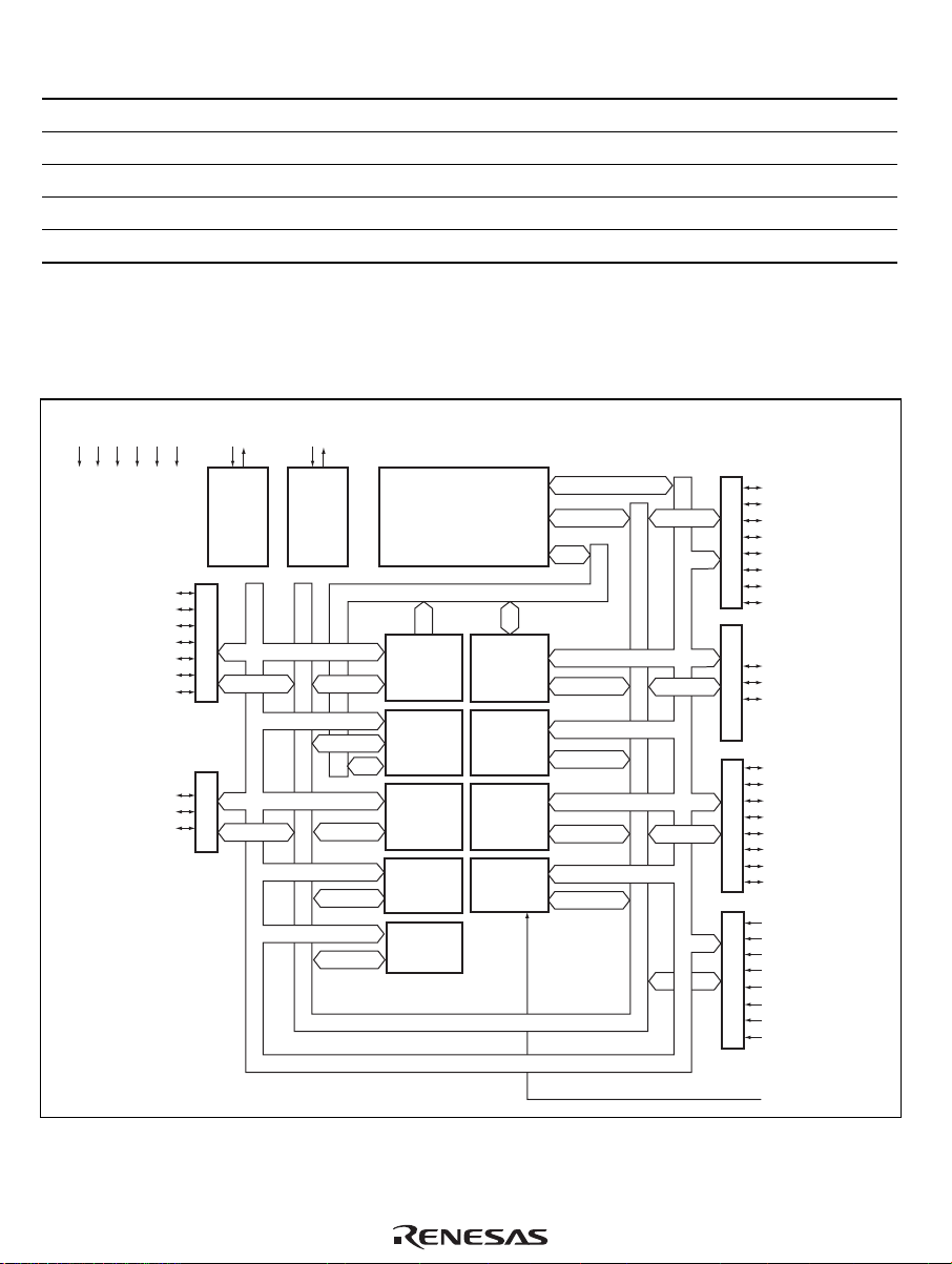
• Compact package
G
Package Code Body Size Pin Pitch
LQFP-64 FP-64E 10.0
× 10.0 mm 0.5 mm
QFP-64 FP-64A 14.0 × 14.0 mm 0.8 mm
LQFP-48 FP-48F 10.0 × 10.0 mm 0.65 mm
LQFP-48 FP-48B 7.0 × 7.0 mm 0.5 mm
SDIP-42 DP-42S 14.0 × 37.3 mm 1.78 mm
Only LQFP-64 (FP-64E) for H8/3664N package
1.2 Internal Block Diagram
VCCVSSVCLRES
P10/TMOW
P11
P12
P14/IRQ0
P15/IRQ1
P16/IRQ2
P17/IRQ3/TRGV
P20/SCK3
P21/RXD
P22/TXD
TEST
NMI
X1
Subclock
generator
Port 1
Port 2
OSC1
System
clock
generator
OSC2
CPU
H8/300H
Data bus (lower)
ROM
Timer W
Timer A
Timer V
2
I
C bus
interface
Data bus (upper)
Address bus
RAM
SCI3
Watchdog
timer
A/D
converter
P80/FTCI
P81/FTIOA
P82/FTIOB
P83/FTIOC
P84/FTIOD
P85
P86
P87
P74/TMRIV
P75/TMCIV
P76/TMOV
P50/WKP0
P51/WKP1
P52/WKP2
P53/WKP3
P54/WKP4
P55/WKP5/ADTR
P56/SDA
P57/SCL
PB0/AN0
PB1/AN1
PB2/AN2
PB3/AN3
PB4/AN4
Port B Port 5 Port 7 Port 8
PB5/AN5
PB6/AN6
PB7/AN7
AV
CC
X2
Figure 1.1 Internal Block Diagram of H8/3664 of F-ZTATTM and Mask-ROM Versions
Rev. 5.00, 03/04, page 2 of 388
Page 31

G
VCCVSSVCLRES
P10/TMOW
P11
P12
P14/IRQ0
P15/IRQ1
P16/IRQ2
P17/IRQ3/TRGV
TEST
NMI
X1
Subclock
generator
Port 1
OSC1
System
clock
generator
OSC2
CPU
H8/300H
Data bus (lower)
ROM
RAM
Port 7 Port 8
P80/FTCI
P81/FTIOA
P82/FTIOB
P83/FTIOC
P84/FTIOD
P85
P86
P87
P74/TMRIV
P75/TMCIV
P76/TMOV
X2
P20/SCK3
P21/RXD
P22/TXD
SDA
SCL
Port 2
C bus
2
I
Timer W
Timer A
Timer V
2
I
C bus
interface
Data bus (upper)
SCI3
Watchdog
timer
A/D
converter
P50/WKP0
P51/WKP1
P52/WKP2
P53/WKP3
Port 5
P54/WKP4
P55/WKP5/ADTR
PB0/AN0
PB1/AN1
PB2/AN2
PB3/AN3
PB4/AN4
Port B
PB5/AN5
PB6/AN6
PB7/AN7
Address bus
AV
CC
EEPROM
Note : The H8/3664N is a stacked-structure product in which an EEPROM chip is mounted on the
H8/3664F-ZTAT
Figure 1.2 Internal Block Diagram of H8/3664N of F-ZTATTM Version with EEPROM
TM
version.
Rev. 5.00, 03/04, page 3 of 388
Page 32

1.3 Pin Arrangement
G
NCNCP22/TXD
48 47 46 45 44 43 42 41 40 39 38 37 36 35 34 33
49
NC
50
NC
NC
NC
51
52
53
54
55
56
57
58
59
60
61
62
63
64
1 2 3 4 5 6 7 8 9 10 11 12 13 14 15 16
NC
P14/IRQ0
P15/IRQ1
P16/IRQ2
P17/IRQ3/TRGV
PB4/AN4
PB5/AN5
PB6/AN6
PB7/AN7
PB3/AN3
PB2/AN2
PB1/AN1
PB0/AN0
Note: Do not connect NC pins (* these pins are not connected to the internal circuitry).
NC
CC
AV
P21/RXD
P20/SCK3
X2
X1
P87
CL
V
P86
P85
H8/3664
Top view
RES
TEST
P84/FTIOD
P83/FTIOC
P82/FTIOB
SS
V
OSC2
OSC1
P81/FTIOA
P80/FTCI
NMINCNC
CC
V
P50/WKP0
P51/WKP1
NC
32
31
30
29
28
27
26
25
24
23
22
21
20
19
18
17
NC
NC
NC
P76/TMOV
P75/TMCIV
P74/TMRIV
P57/SCL
P56/SDA
P12
P11
P10/TMOW
P55/WKP5/ADTR
P54/WKP4
P53/WKP3
P52/WKP2
NC
NC
Figure 1.3 Pin Arrangement of H8/3664 of F-ZTATTM and Mask-ROM Versions
(FP-64E, FP-64A)
Rev. 5.00, 03/04, page 4 of 388
Page 33

P14/IRQ0
G
P15/IRQ1
P16/IRQ2
P17/IRQ3/TRGV
PB4/AN4
PB5/AN5
PB6/AN6
PB7/AN7
PB3/AN3
PB2/AN2
PB1/AN1
PB0/AN0
P22/TXD
P21/RXD
P20/SCK3
P87
P86
P85
P84/FTIOD
P83/FTIOC
P82/FTIOB
P81/FTIOA
36 35 34 33 32 31 30 29 28 27 26 25
37
38
39
40
41
42
43
44
45
46
47
48
123456789101112
H8/3664
Top View
P80/FTCI
NMI
24
23
22
21
20
19
18
17
16
15
14
13
P76/TMOV
P75/TMCIV
P74/TMRIV
P57/SCL
P56/SDA
P12
P11
P10/TMOW
P55/WKP5/ADTR
P54/WKP4
P53/WKP3
P52/WKP2
AVcc
X2
X1
CL
V
RES
TEST
SS
V
OSC2
OSC1
Vcc
P50/WKP0
P51/WKP1
Figure 1.4 Pin Arrangement of H8/3664 of F-ZTATTM and Mask-ROM Versions
(FP-48F, FP-48B)
Rev. 5.00, 03/04, page 5 of 388
Page 34

PB3/AN3
PB2/AN2
PB1/AN1
PB0/AN0
AV
X2
X1
V
RES
TEST
V
OSC2
OSC1
V
P50/WKP0
P51/WKP1
P52/WKP2
P53/WKP3
P54/WKP4
P55/WKP5/ADTRG
P10/TMOW
1
2
3
4
5
CC
6
7
8
CL
9
10
11
SS
12
13
14
CC
15
16
17
18
19
20
21
H8/3664
Top view
42
41
40
39
38
37
36
35
34
33
32
31
30
29
28
27
26
25
24
23
22
P17/IRQ3/TRGV
P16/IRQ2
P15/IRQ1
P14/IRQ0
P22/TXD
P21/RXD
P20/SCK3
P87
P86
P85
P84/FTIOD
P83/FTIOC
P82/FTIOB
P81/FTIOA
P80/FTCI
NMI
P76/TMOV
P75/TMCIV
P74/TMRIV
P57/SCL
P56/SDA
Note: DP-42S has no P11, P12, PB4/AN4, PB5/AN5, PB6/AN6, and PB7/AN7 pins.
Figure 1.5 Pin Arrangement of H8/3664 of F-ZTATTM and Mask-ROM Versions
(DS-42S)
Rev. 5.00, 03/04, page 6 of 388
Page 35

NCNCP22/TXD
G
P21/RXD
P20/SCK3
P87
P86
P85
P84/FTIOD
P83/FTIOC
P82/FTIOB
P81/FTIOA
P80/FTCI
NMINCNC
48 47 46 45 44 43 42 41 40 39 38 37 36 35 34 33
49
NC
50
NC
NC
NC
51
52
53
54
55
56
57
58
59
60
61
62
63
64
1 2 3 4 5 6 7 8 9 10111213141516
NC
AVcc
X2
NC
X1
H8/3664N
Top View
CL
V
RES
TEST
SS
V
OSC2
OSC1
Vcc
P50/WKP0
P14/IRQ0
P15/IRQ1
P16/IRQ2
P17/IRQ3/TRGV
PB4/AN4
PB5/AN5
PB6/AN6
PB7/AN7
PB3/AN3
PB2/AN2
PB1/AN1
PB0/AN0
Note: Do not connect NC pins.
* These pins are only available for the I2C bus interface in the F-ZATTM version with EEPROM.
P51/WKP1
NC
32
31
30
29
28
27
26
25
24
23
22
21
20
19
18
17
NC
NC
NC
P76/TMOV
P75/TMCIV
P74/TMRIV
SCL*
SDA*
P12
P11
P10/TMOW
P55/WKP5/ADTR
P54/WKP4
P53/WKP3
P52/WKP2
NC
NC
Figure 1.6 Pin Arrangement of H8/3664N of F-ZTATTM Version with EEPROM
(FP-64E)
Rev. 5.00, 03/04, page 7 of 388
Page 36

1.4 Pin Functions
Table 1.1 Pin Functions
Pin No.
H8/3664 H8/3664N
FP-64E,
Type Symbol
Power source
pins
V
AVCC 3 1 5 3 Input Analog power supply pin for the A/D
V
Clock pins OSC1 11 9 13 11 Input
OSC2 10 8 12 10 Output
X1 5 3 7 5 Input For connection to a 32.768 kHz crystal
X2 4 2 6 4 Output
System control RES 7 5 9 7 Input Reset pin. When this driven low, the chip
TEST 8 6 10 8 Input Test pin. Connect this pin to Vss.
Interrupt pins NMI 35 25 27 35 Input Non-maskable interrupt request input pin.
IRQ0 to
WKP0 to
VCC 12 10 14 12 Input Power supply pin. Connect this pin to the
SS
CL
IRQ3
WKP5
FP-64A
9 7 11 9 Input Ground pin. Connect all these pins to the
6 4 8 6 Input Internal step-down power supply pin.
51 to 54 37 to 40 39 to 42 51 to 54 Input External interrupt request input pins. Can
13, 14,
19 to 22
FP-48F,
FP-48B DP-42S FP-64E I/O Functions
system power supply.
system power supply (0V).
converter. When the A/D converter is not
used, connect this pin to the system
power supply.
Connect a
capacitor of around 0.1 µF between this
pin and
the Vss pin for stabilization.
These pins connect to a crystal or ceramic
resonator for system clocks, or can be
used to input an external clock.
These pins can be used to input an
external clock.
See section 5, Clock Pulse Generators,
for a typical connection.
resonator for subclocks.
See section 5, Clock Pulse Generators,
for a typical connection.
is reset.
Be sure to pull-up by a pull-up resistor.
select the rising or falling edge.
11 to 16 15 to 20 13, 14,
19 to 22
Input External interrupt request input pins. Can
select the rising or falling edge.
Rev. 5.00, 03/04, page 8 of 388
Page 37

Pin No.
H8/3664 H8/3664N
FP-64E,
Type Symbol
Timer A TMOW 23 17 21 23 Output This is an output pin for divided clocks.
Timer V TMOV 30 24 26 30 Output This is an output pin for waveforms
TMCIV 29 23 25 29 Input External event input pin.
TMRIV 28 22 24 28 Input Counter reset input pin.
TRGV 54 40 42 54 Input Counter start trigger input pin.
Timer W FTCI 36 26 28 36 Input External event input pin.
FTIOA to
FTIOD
I2C bus
inerface
SCL 27*2 21 23 27*1 I/O
Serial commu-
nication
interface (SCI)
SCK3 44 34 36 44 I/O Clock I/O pin
A/D converter AN7 to
ADTRG 22 16 20 22 Input A/D converter trigger input pin.
I/O ports PB7 to
P17 to
P22 to
P57 to
SDA 26*2 20 22 26*1 I/O IIC data I/O pin. Can directly drive a bus
TXD 46 36 38 46 Output Transmit data output pin
RXD 45 35 37 45 Input Receive data input pin
AN0
PB0
P14,
P12 to
P10
P20
P50 (P55
to P50 for
H8/3664N)
FP-64A
37 to 40 27 to 30 29 to 32 37 to 40 I/O Output compare output/ input capture
55 to 62 41 to 48 1 to 4*2 55 to 62 Input Analog input pin
55 to 62 41 to 48 1 to 4*2 55 to 62 Input 8-bit input port.
51 to 54
23 to 25
44 to 46 34 to 36 36 to 38 44 to 46 I/O 3-bit I/O port.
13,14,
19 to 22
26, 27
FP-48F,
FP-48B DP-42S FP-64E I/O Functions
generated by the output compare function.
input/ PWM output pin
by NMOS open-drain output. When using
this pin, external pull-up resistance is
required.
IIC clock I/O pin. Can directly drive a bus
37 to 40
17 to 19
21, 20,
16 to 11
39 to 42,
2
21*
15 to 20,
22, 23
51 to 54,
23 to 25
13, 14,
19 to 22
(EEPROM:
input)
I/O 7-bit I/O port.
I/O 8-bit I/O port
by NMOS open-drain output. When using
this pin, external pull-up resistance is
required.
(6-bit I/O port for H8/3664N)
Rev. 5.00, 03/04, page 9 of 388
Page 38

Pin No.
H8/3664 H8/3664N
FP-64E,
Type Symbol
I/O ports P76 to
P74
P87 to
P80
Note : 1. These pins are only available for the I2C bus interface in the F-ZATTM version with EEPROM. Since
the I
FP-64A
28 to 30 22 to 24 24 to 26 28 to 30 I/O 3-bit I/O port
36 to 43 26 to 33 28 to 35 36 to 43 I/O 8-bit I/O port.
2
C bus is disabled after canceling a reset, the ICE bit in ICCR must be set to 1 by using the
FP-48F,
FP-48B DP-42S FP-64E I/O Functions
program.
2. The DP-42S does not have the P11, P12, PB4/AN4, PB5/AN5, PB6/AN6, and PB7/AN7 pins.
Rev. 5.00, 03/04, page 10 of 388
Page 39

Section 2 CPU
This LSI has an H8/300H CPU with an internal 32-bit architecture that is upward-compatible with
the H8/300CPU, and supports only normal mode, which has a 64-kbyte address space.
• Upward-compatible with H8/300 CPUs
Can execute H8/300 CPUs object programs
Additional eight 16-bit extended registers
32-bit transfer and arithmetic and logic instructions are added
Signed multiply and divide instructions are added.
• General-register architecture
Sixteen 16-bit general registers also usable as sixteen 8-bit registers or eight 32-bit registers
• Sixty-two basic instructions
8/16/32-bit data transfer and arithmetic and logic instructions
Multiply and divide instructions
Powerful bit-manipulation instructions
• Eight addressing modes
Register direct [Rn]
Register indirect [@ERn]
Register indirect with displacement [@(d:16,ERn) or @(d:24,ERn)]
Register indirect with post-increment or pre-decrement [@ERn+ or @–ERn]
Absolute address [@aa:8, @aa:16, @aa:24]
Immediate [#xx:8, #xx:16, or #xx:32]
Program-counter relative [@(d:8,PC) or @(d:16,PC)]
Memory indirect [@@aa:8]
• 64-kbyte address space
• High-speed operation
All frequently-used instructions execute in one or two states
8/16/32-bit register-register add/subtract : 2 state
8 × 8-bit register-register multiply : 14 states
16 ÷ 8-bit register-register divide : 14 states
16 × 16-bit register-register multiply : 22 states
32 ÷ 16-bit register-register divide : 22 states
• Power-down state
Transition to power-down state by SLEEP instruction
CPU30H2A_000020020300 Rev. 5.00, 03/04, page 11 of 388
Page 40

2.1 Address Space and Memory Map
The address space of this LSI is 64 kbytes, which includes the program area and the data area.
Figures 2.1 show the memory map.
(Flash memory version)
H'0000
H'0033
H'0034
H'7FFF
HD64F3664
Interrupt vector
On-chip ROM
(32 kbytes)
Not used
H'0000
H'0033
H'0034
H'1FFF
HD6433660
(Mask ROM version)
Interrupt vector
On-chip ROM
(8 kbytes)
Not used
H'0000
H'0033
H'0034
H'2FFF
HD6433661
(Mask ROM version)
Interrupt vector
On-chip ROM
(12 kbytes)
Not used
H'F780
(1-kbyte work area
for flash memory
programming)
H'FB7F
H'FB80
H'FF7F
H'FF80
H'FFFF
On-chip RAM
(2 kbytes)
(1-kbyte user area)
Internal I/O register
Rev. 5.00, 03/04, page 12 of 388
H'FD80
H'FF7F
H'FF80
H'FFFF
On-chip RAM
(512 bytes)
Internal I/O register
Figure 2.1 Memory Map (1)
H'FD80
H'FF7F
H'FF80
H'FFFF
On-chip RAM
(512 bytes)
Internal I/O register
Page 41

H'0000
H'0033
H'0034
HD6433662
(Mask ROM version)
Interrupt vector
On-chip ROM
(16 kbytes)
H'0000
H'0033
H'0034
HD6433663
(Mask ROM version)
Interrupt vector
On-chip ROM
(24 kbytes)
H'0000
H'0033
H'0034
HD6433664
(Mask ROM version)
Interrupt vector
H'3FFF
Not used
H'5FFF
H'FB80
On-chip ROM
(32 kbytes)
H'7FFF
Not used
Not used
H'FB80
H'FD80
H'FF7F
H'FF80
H'FFFF
On-chip RAM
(512 bytes)
Internal I/O register
On-chip RAM
(1 kbyte)
H'FF7F
H'FF80
Internal I/O register
H'FFFF
Figure 2.1 Memory Map (2)
On-chip RAM
(1 kbyte)
H'FF7F
H'FF80
Internal I/O register
H'FFFF
Rev. 5.00, 03/04, page 13 of 388
Page 42

HD64N3664
(On-chip EEPROM module)
User area
(512 bytes)
Not used
Slave address
register
H'0000
H'01FF
H'FF09
Not used
Figure 2.1 Memory Map (3)
Rev. 5.00, 03/04, page 14 of 388
Page 43
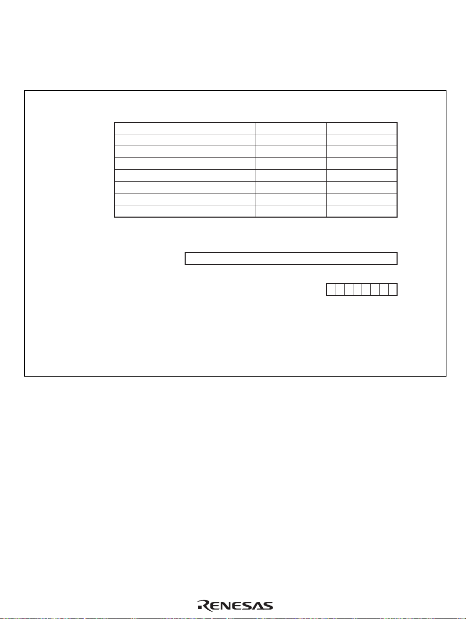
2.2 Register Configuration
The H8/300H CPU has the internal registers shown in figure 2.2. There are two types of registers;
general registers and control registers. The control registers are a 24-bit program counter (PC), and
an 8-bit condition code register (CCR).
General Registers
15 0 7 0 7 0
ER0
ER1
ER2
ER3
ER4
ER5
ER6
ER7 (SP)
E0
E1
E2
E3
E4
E5
E6
E7
R0H
R1H
R2H
R3H
R4H
R5H
R6H
R7H
R0L
R1L
R2L
R3L
R4L
R5L
R6L
R7L
Control Registers (CR)
Legend
:Stack pointer
SP
:Program counter
PC
:Condition-code register
CCR
:Interrupt mask bit
I
:User bit
UI
23 0
PC
76543210
CCR
IUIHUNZVC
:Half-carry flag
H
:User bit
U
:Negative flag
N
:Zero flag
Z
:Overflow flag
V
:Carry flag
C
Figure 2.2 CPU Registers
Rev. 5.00, 03/04, page 15 of 388
Page 44
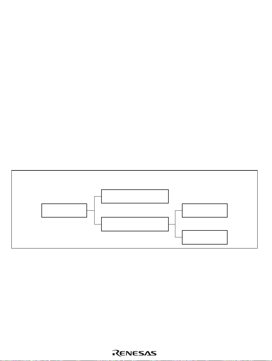
2.2.1 General Registers
The H8/300H CPU has eight 32-bit general registers. These general registers are all functionally
identical and can be used as both address registers and data registers. When a general register is
used as a data register, it can be accessed as a 32-bit, 16-bit, or 8-bit register. Figure 2.3 illustrates
the usage of the general registers. When the general registers are used as 32-bit registers or address
registers, they are designated by the letters ER (ER0 to ER7).
The ER registers divide into 16-bit general registers designated by the letters E (E0 to E7) and R
(R0 to R7). These registers are functionally equivalent, providing a maximum of sixteen 16-bit
registers. The E registers (E0 to E7) are also referred to as extended registers.
The R registers divide into 8-bit registers designated by the letters RH (R0H to R7H) and RL (R0L
to R7L). These registers are functionally equivalent, providing a maximum of sixteen 8-bit
registers.
The usage of each register can be selected independently.
General register ER7 has the function of stack pointer (SP) in addition to its general-register
function, and is used implicitly in exception handling and subroutine calls. Figure 2.4 shows the
stack.
• Address registers
• 32-bit registers
ER registers
(ER0 to ER7)
Figure 2.3 Usage of General Registers
Rev. 5.00, 03/04, page 16 of 388
• 16-bit registers • 8-bit registers
E registers (extended registers)
(E0 to E7)
R registers
(R0 to R7)
RH registers
(R0H to R7H)
RL registers
(R0L to R7L)
Page 45

Free area
SP (ER7)
Stack area
Figure 2.4 Relationship between Stack Pointer and Stack Area
2.2.2 Program Counter (PC)
This 24-bit counter indicates the address of the next instruction the CPU will execute. The length
of all CPU instructions is 2 bytes (one word), so the least significant PC bit is ignored. (When an
instruction is fetched, the least significant PC bit is regarded as 0). The PC is initialized when the
start address is loaded by the vector address generated during reset exception-handling sequence.
2.2.3 Condition-Code Register (CCR)
This 8-bit register contains internal CPU status information, including an interrupt mask bit (I) and
half-carry (H), negative (N), zero (Z), overflow (V), and carry (C) flags. The I bit is initialized to 1
by reset exception-handling sequence, but other bits are not initialized.
Some instructions leave flag bits unchanged. Operations can be performed on the CCR bits by the
LDC, STC, ANDC, ORC, and XORC instructions. The N, Z, V, and C flags are used as branching
conditions for conditional branch (Bcc) instructions.
For the action of each instruction on the flag bits, see appendix A.1 Instruction List.
Rev. 5.00, 03/04, page 17 of 388
Page 46

Bit Bit Name Initial Value R/W Description
7 I 1 R/W Interrupt Mask Bit
Masks interrupts other than NMI when set to 1.
NMI is accepted regardless of the I bit setting.
The I bit is set to 1 at the start of an exceptionhandling sequence.
6 UI undefined R/W User Bit
Can be written and read by software using the
LDC, STC, ANDC, ORC, and XORC instructions.
5 H undefined R/W Half-Carry Flag
When the ADD.B, ADDX.B, SUB.B, SUBX.B,
CMP.B, or NEG.B instruction is executed, this
flag is set to 1 if there is a carry or borrow at bit 3,
and cleared to 0 otherwise. When the ADD.W,
SUB.W, CMP.W, or NEG.W instruction is
executed, the H flag is set to 1 if there is a carry
or borrow at bit 11, and cleared to 0 otherwise.
When the ADD.L, SUB.L, CMP.L, or NEG.L
instruction is executed, the H flag is set to 1 if
there is a carry or borrow at bit 27, and cleared to
0 otherwise.
4 U undefined R/W User Bit
Can be written and read by software using the
LDC, STC, ANDC, ORC, and XORC instructions.
3 N undefined R/W Negative Flag
Stores the value of the most significant bit of data
as a sign bit.
2 Z undefined R/W Zero Flag
Set to 1 to indicate zero data, and cleared to 0 to
indicate non-zero data.
1 V undefined R/W Overflow Flag
Set to 1 when an arithmetic overflow occurs, and
cleared to 0 at other times.
0 C undefined R/W Carry Flag
Set to 1 when a carry occurs, and cleared to 0
otherwise. Used by:
• Add instructions, to indicate a carry
• Subtract instructions, to indicate a borrow
• Shift and rotate instructions, to indicate a
carry
The carry flag is also used as a bit accumulator
by bit manipulation instructions.
Rev. 5.00, 03/04, page 18 of 388
Page 47
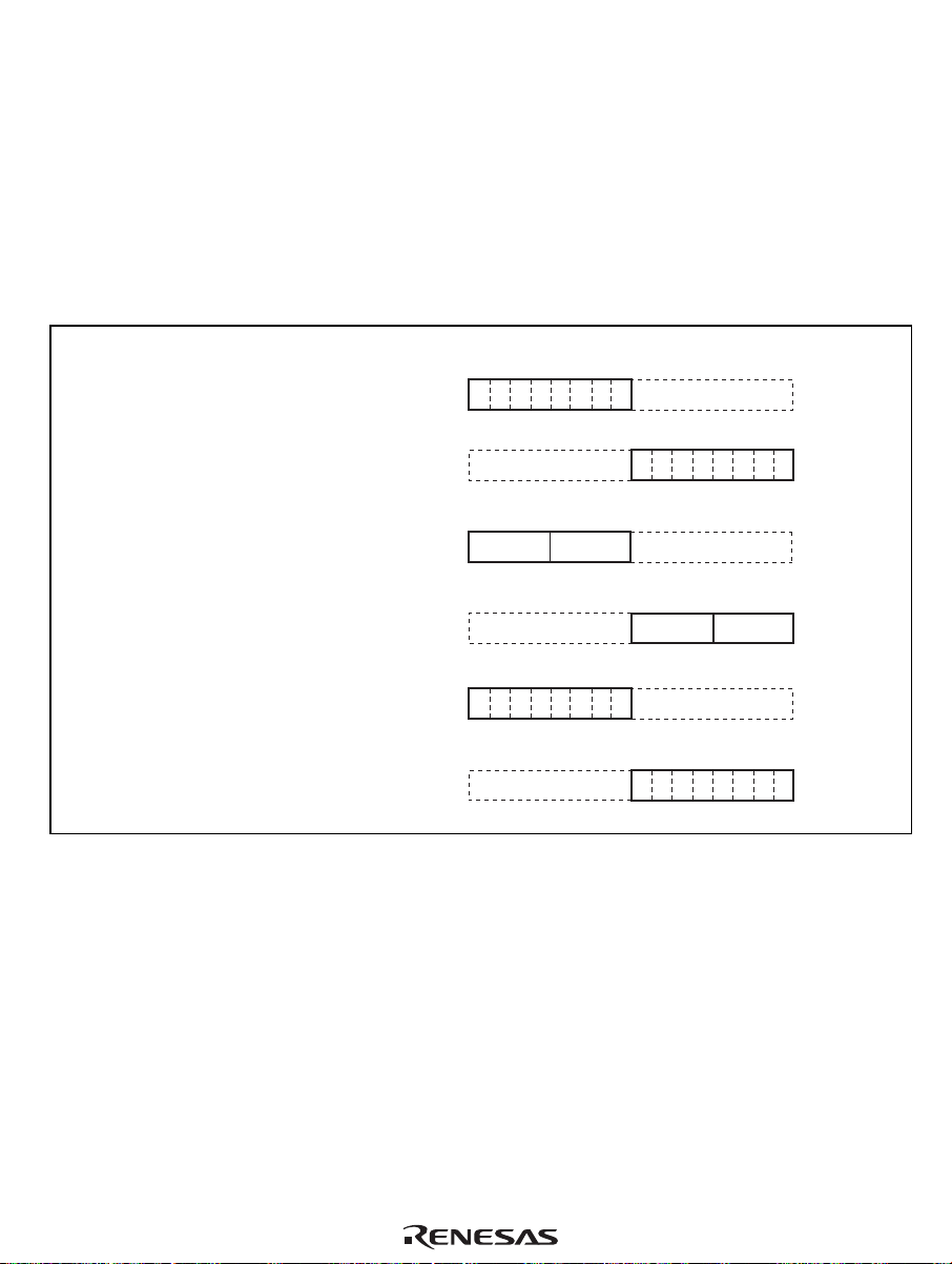
2.3 Data Formats
The H8/300H CPU can process 1-bit, 4-bit (BCD), 8-bit (byte), 16-bit (word), and 32-bit
(longword) data. Bit-manipulation instructions operate on 1-bit data by accessing bit n (n = 0, 1, 2,
…, 7) of byte operand data. The DAA and DAS decimal-adjust instructions treat byte data as two
digits of 4-bit BCD data.
2.3.1 General Register Data Formats
Figure 2.5 shows the data formats in general registers.
Data Type General Register Data Format
70
6543271
Don't care
0
1-bit data
RnH
1-bit data
4-bit BCD data
4-bit BCD data
Byte data
Byte data
7
RnL
RnH
RnL
RnH
RnL
Don't care
7 04 3
Upper Lower
Don't care
7 0
MSB LSB
Don't care
65432710
Don't care
704 3
Upper Lower
7
MSB LSB
Figure 2.5 General Register Data Formats (1)
0
Don't care
0
Rev. 5.00, 03/04, page 19 of 388
Page 48

Data Type Data FormatGeneral
Register
Word data
Word dataRnEn
Longword
ERn
data
Legend
ERn
: General register ER
En
: General register E
Rn
: General register R
RnH
: General register RH
RnL
: General register RL
MSB
: Most significant bit
LSB
: Least significant bit
15 0
MSB LSB
15 0
MSB LSB
31 16
MSB
15 0
Figure 2.5 General Register Data Formats (2)
LSB
Rev. 5.00, 03/04, page 20 of 388
Page 49

2.3.2 Memory Data Formats
Figure 2.6 shows the data formats in memory. The H8/300H CPU can access word data and
longword data in memory, however word or longword data must begin at an even address. If an
attempt is made to access word or longword data at an odd address, an address error does not
occur, however the least significant bit of the address is regarded as 0, so access begins the
preceding address. This also applies to instruction fetches.
When ER7 (SP) is used as an address register to access the stack, the operand size should be word
or longword.
Data Type Address
1-bit data
Byte data
Word data
Longword data Address 2N
Address L
Address L
Address 2M
Address 2M+1
Address 2N+1
Address 2N+2
Address 2N+3
Figure 2.6 Memory Data Formats
Data Format
70
76 543210
MSB
MSB
MSB
LSB
LSB
LSB
Rev. 5.00, 03/04, page 21 of 388
Page 50

2.4 Instruction Set
2.4.1 Table of Instructions Classified by Function
The H8/300H CPU has 62 instructions. Tables 2.2 to 2.9 summarize the instructions in each
functional category. The notation used in tables 2.2 to 2.9 is defined below.
Table 2.1 Operation Notation
Symbol Description
Rd General register (destination)*
Rs General register (source)*
Rn General register*
ERn General register (32-bit register or address register)
(EAd) Destination operand
(EAs) Source operand
CCR Condition-code register
N N (negative) flag in CCR
Z Z (zero) flag in CCR
V V (overflow) flag in CCR
C C (carry) flag in CCR
PC Program counter
SP Stack pointer
#IMM Immediate data
disp Displacement
+ Addition
– Subtraction
× Multiplication
÷ Division
∧ Logical AND
∨ Logical OR
⊕ Logical XOR
→ Move
¬ NOT (logical complement)
:3/:8/:16/:24 3-, 8-, 16-, or 24-bit length
Note: * General registers include 8-bit registers (R0H to R7H, R0L to R7L), 16-bit registers (R0 to
R7, E0 to E7), and 32-bit registers/address register (ER0 to ER7).
Rev. 5.00, 03/04, page 22 of 388
Page 51

Table 2.2 Data Transfer Instructions
Instruction Size* Function
MOV B/W/L (EAs) → Rd, Rs → (EAd)
Moves data between two general registers or between a general register
and memory, or moves immediate data to a general register.
MOVFPE B (EAs) → Rd, Cannot be used in this LSI.
MOVTPE B Rs → (EAs) Cannot be used in this LSI.
POP W/L @SP+ → Rn
Pops a general register from the stack. POP.W Rn is identical to MOV.W
@SP+, Rn. POP.L ERn is identical to MOV.L @SP+, ERn.
PUSH W/L Rn → @–SP
Pushes a general register onto the stack. PUSH.W Rn is identical to
MOV.W Rn, @–SP. PUSH.L ERn is identical to MOV.L ERn, @–SP.
Note: * Refers to the operand size.
B: Byte
W: Word
L: Longword
Rev. 5.00, 03/04, page 23 of 388
Page 52

Table 2.3 Arithmetic Operations Instructions (1)
Instruction Size* Function
ADD
SUB
ADDX
SUBX
INC
DEC
ADDS
SUBS
DAA
DAS
MULXU B/W Rd × Rs → Rd
MULXS B/W Rd × Rs → Rd
DIVXU B/W Rd ÷ Rs → Rd
Note: * Refers to the operand size.
B: Byte
W: Word
L: Longword
B/W/L Rd ± Rs → Rd, Rd ± #IMM → Rd
Performs addition or subtraction on data in two general registers, or on
immediate data and data in a general register (immediate byte data
cannot be subtracted from byte data in a general register. Use the SUBX
or ADD instruction.)
B Rd ± Rs ± C → Rd, Rd ± #IMM ± C → Rd
Performs addition or subtraction with carry on byte data in two general
registers, or on immediate data and data in a general register.
B/W/L Rd ± 1 → Rd, Rd ± 2 → Rd
Increments or decrements a general register by 1 or 2. (Byte operands
can be incremented or decremented by 1 only.)
L Rd ± 1 → Rd, Rd ± 2 → Rd, Rd ± 4 → Rd
Adds or subtracts the value 1, 2, or 4 to or from data in a 32-bit register.
B Rd decimal adjust → Rd
Decimal-adjusts an addition or subtraction result in a general register by
referring to the CCR to produce 4-bit BCD data.
Performs unsigned multiplication on data in two general registers: either
8 bits × 8 bits → 16 bits or 16 bits × 16 bits → 32 bits.
Performs signed multiplication on data in two general registers: either 8
bits × 8 bits → 16 bits or 16 bits × 16 bits → 32 bits.
Performs unsigned division on data in two general registers: either 16
bits ÷ 8 bits → 8-bit quotient and 8-bit remainder or 32 bits ÷ 16 bits →
16-bit quotient and 16-bit remainder.
Rev. 5.00, 03/04, page 24 of 388
Page 53

Table 2.3 Arithmetic Operations Instructions (2)
Instruction Size* Function
DIVXS B/W Rd ÷ Rs → Rd
Performs signed division on data in two general registers: either 16 bits ÷
8 bits → 8-bit quotient and 8-bit remainder or 32 bits ÷ 16 bits → 16-bit
quotient and 16-bit remainder.
CMP B/W/L Rd – Rs, Rd – #IMM
Compares data in a general register with data in another general register
or with immediate data, and sets CCR bits according to the result.
NEG B/W/L 0 – Rd → Rd
Takes the two's complement (arithmetic complement) of data in a
general register.
EXTU W/L Rd (zero extension) → Rd
Extends the lower 8 bits of a 16-bit register to word size, or the lower 16
bits of a 32-bit register to longword size, by padding with zeros on the
left.
EXTS W/L Rd (sign extension) → Rd
Extends the lower 8 bits of a 16-bit register to word size, or the lower 16
bits of a 32-bit register to longword size, by extending the sign bit.
Note: * Refers to the operand size.
B: Byte
W: Word
L: Longword
Rev. 5.00, 03/04, page 25 of 388
Page 54

Table 2.4 Logic Operations Instructions
Instruction Size* Function
AND B/W/L Rd ∧ Rs → Rd, Rd ∧ #IMM → Rd
Performs a logical AND operation on a general register and another
general register or immediate data.
OR B/W/L Rd ∨ Rs → Rd, Rd ∨ #IMM → Rd
Performs a logical OR operation on a general register and another
general register or immediate data.
XOR B/W/L Rd ⊕ Rs → Rd, Rd ⊕ #IMM → Rd
Performs a logical exclusive OR operation on a general register and
another general register or immediate data.
NOT B/W/L ¬ (Rd) → (Rd)
Takes the one's complement of general register contents.
Note: * Refers to the operand size.
B: Byte
W: Word
L: Longword
Table 2.5 Shift Instructions
Instruction Size* Function
SHAL
SHAR
SHLL
SHLR
ROTL
ROTR
ROTXL
ROTXR
Note: * Refers to the operand size.
B: Byte
W: Word
L: Longword
B/W/L Rd (shift) → Rd
Performs an arithmetic shift on general register contents.
B/W/L Rd (shift) → Rd
Performs a logical shift on general register contents.
B/W/L Rd (rotate) → Rd
Rotates general register contents.
B/W/L Rd (rotate) → Rd
Rotates general register contents through the carry flag.
Rev. 5.00, 03/04, page 26 of 388
Page 55

Table 2.6 Bit Manipulation Instructions (1)
Instruction Size* Function
BSET B 1 → (<bit-No.> of <EAd>)
Sets a specified bit in a general register or memory operand to 1. The bit
number is specified by 3-bit immediate data or the lower three bits of a
general register.
BCLR B 0 → (<bit-No.> of <EAd>)
Clears a specified bit in a general register or memory operand to 0. The
bit number is specified by 3-bit immediate data or the lower three bits of a
general register.
BNOT B ¬ (<bit-No.> of <EAd>) → (<bit-No.> of <EAd>)
Inverts a specified bit in a general register or memory operand. The bit
number is specified by 3-bit immediate data or the lower three bits of a
general register.
BTST B ¬ (<bit-No.> of <EAd>) → Z
Tests a specified bit in a general register or memory operand and sets or
clears the Z flag accordingly. The bit number is specified by 3-bit
immediate data or the lower three bits of a general register.
BAND
BIAND
BOR
BIOR
Note: * Refers to the operand size.
B: Byte
B
B
B
B
C ∧ (<bit-No.> of <EAd>) → C
ANDs the carry flag with a specified bit in a general register or memory
operand and stores the result in the carry flag.
C ∧ ¬ (<bit-No.> of <EAd>) → C
ANDs the carry flag with the inverse of a specified bit in a general
register or memory operand and stores the result in the carry flag.
The bit number is specified by 3-bit immediate data.
C ∨ (<bit-No.> of <EAd>) → C
ORs the carry flag with a specified bit in a general register or memory
operand and stores the result in the carry flag.
C ∨ ¬ (<bit-No.> of <EAd>) → C
ORs the carry flag with the inverse of a specified bit in a general register
or memory operand and stores the result in the carry flag.
The bit number is specified by 3-bit immediate data.
Rev. 5.00, 03/04, page 27 of 388
Page 56

Table 2.6 Bit Manipulation Instructions (2)
Instruction Size* Function
BXOR
BIXOR
BLD
BILD
BST
BIST
Note: * Refers to the operand size.
B: Byte
B
B
B
B
B
B
C ⊕ (<bit-No.> of <EAd>) → C
XORs the carry flag with a specified bit in a general register or memory
operand and stores the result in the carry flag.
C ⊕ ¬ (<bit-No.> of <EAd>) → C
XORs the carry flag with the inverse of a specified bit in a general
register or memory operand and stores the result in the carry flag.
The bit number is specified by 3-bit immediate data.
(<bit-No.> of <EAd>) → C
Transfers a specified bit in a general register or memory operand to the
carry flag.
¬ (<bit-No.> of <EAd>) → C
Transfers the inverse of a specified bit in a general register or memory
operand to the carry flag.
The bit number is specified by 3-bit immediate data.
C → (<bit-No.> of <EAd>)
Transfers the carry flag value to a specified bit in a general register or
memory operand.
¬ C → (<bit-No.> of <EAd>)
Transfers the inverse of the carry flag value to a specified bit in a general
register or memory operand.
The bit number is specified by 3-bit immediate data.
Rev. 5.00, 03/04, page 28 of 388
Page 57

Table 2.7 Branch Instructions
Instruction Size Function
Bcc* — Branches to a specified address if a specified condition is true. The
branching conditions are listed below.
Mnemonic Description Condition
BRA (BT) Always (true) Always
BRN (BF) Never (false) Never
BHI High C ∨ Z = 0
BLS Low or same C ∨ Z = 1
BCC (BHS) Carry clear
(high or same)
BCS (BLO) Carry set (low) C = 1
BNE Not equal Z = 0
BEQ Equal Z = 1
BVC Overflow clear V = 0
BVS Overflow set V = 1
BPL Plus N = 0
BMI Minus N = 1
BGE Greater or equal N ⊕ V = 0
BLT Less than N ⊕ V = 1
BGT Greater than Z∨(N ⊕ V) = 0
BLE Less or equal Z∨(N ⊕ V) = 1
JMP — Branches unconditionally to a specified address.
BSR — Branches to a subroutine at a specified address.
JSR — Branches to a subroutine at a specified address.
RTS — Returns from a subroutine
Note: * Bcc is the general name for conditional branch instructions.
C = 0
Rev. 5.00, 03/04, page 29 of 388
Page 58

Table 2.8 System Control Instructions
Instruction Size* Function
TRAPA — Starts trap-instruction exception handling.
RTE — Returns from an exception-handling routine.
SLEEP — Causes a transition to a power-down state.
LDC B/W (EAs) → CCR
Moves the source operand contents to the CCR. The CCR size is one
byte, but in transfer from memory, data is read by word access.
STC B/W CCR → (EAd), EXR → (EAd)
Transfers the CCR contents to a destination location. The condition code
register size is one byte, but in transfer to memory, data is written by
word access.
ANDC B CCR ∧ #IMM → CCR, EXR ∧ #IMM → EXR
Logically ANDs the CCR with immediate data.
ORC B CCR ∨ #IMM → CCR, EXR ∨ #IMM → EXR
Logically ORs the CCR with immediate data.
XORC B CCR ⊕ #IMM → CCR, EXR ⊕ #IMM → EXR
Logically XORs the CCR with immediate data.
NOP — PC + 2 → PC
Only increments the program counter.
Note: * Refers to the operand size.
B: Byte
W: Word
Rev. 5.00, 03/04, page 30 of 388
Page 59

Table 2.9 Block Data Transfer Instructions
Instruction Size Function
EEPMOV.B — if R4L ≠ 0 then
Repeat @ER5+ → @ER6+,
R4L–1 → R4L
Until R4L = 0
else next;
EEPMOV.W — if R4 ≠ 0 then
Repeat @ER5+ → @ER6+,
R4–1 → R4
Until R4 = 0
else next;
Transfers a data block. Starting from the address set in ER5, transfers
data for the number of bytes set in R4L or R4 to the address location set
in ER6.
Execution of the next instruction begins as soon as the transfer is
completed.
2.4.2 Basic Instruction Formats
H8/300H CPU instructions consist of 2-byte (1-word) units. An instruction consists of an
operation field (op field), a register field (r field), an effective address extension (EA field), and a
condition field (cc).
Figure 2.7 shows examples of instruction formats.
Rev. 5.00, 03/04, page 31 of 388
Page 60

• Operation Field
Indicates the function of the instruction, the addressing mode, and the operation to be carried
out on the operand. The operation field always includes the first four bits of the instruction.
Some instructions have two operation fields.
• Register Field
Specifies a general register. Address registers are specified by 3 bits, and data registers by 3
bits or 4 bits. Some instructions have two register fields. Some have no register field.
• Effective Address Extension
8, 16, or 32 bits specifying immediate data, an absolute address, or a displacement. A24-bit
address or displacement is treated as a 32-bit data in which the first 8 bits are 0 (H'00).
• Condition Field
Specifies the branching condition of Bcc instructions.
(1) Operation field only
op
(2) Operation field and register fields
op
(3) Operation field, register fields, and effective address extension
op
EA(disp)
rn
rn rm
rm
NOP, RTS, etc.
ADD.B Rn, Rm, etc.
MOV.B @(d:16, Rn), Rm
(4) Operation field, effective address extension, and condition field
op cc EA(disp) BRA d:8
Rev. 5.00, 03/04, page 32 of 388
Figure 2.7 Instruction Formats
Page 61

2.5 Addressing Modes and Effective Address Calculation
The following describes the H8/300H CPU. In this LSI, the upper eight bits are ignored in the
generated 24-bit address, so the effective address is 16 bits.
2.5.1 Addressing Modes
The H8/300H CPU supports the eight addressing modes listed in table 2.10. Each instruction uses
a subset of these addressing modes. Addressing modes that can be used differ depending on the
instruction. For details, refer to appendix A.4, Combinations of Instructions and Addressing
Modes.
Arithmetic and logic instructions can use the register direct and immediate modes. Data transfer
instructions can use all addressing modes except program-counter relative and memory indirect.
Bit manipulation instructions use register direct, register indirect, or the absolute addressing mode
to specify an operand, and register direct (BSET, BCLR, BNOT, and BTST instructions) or
immediate (3-bit) addressing mode to specify a bit number in the operand.
Table 2.10 Addressing Modes
No. Addressing Mode Symbol
1 Register direct Rn
2 Register indirect @ERn
3 Register indirect with displacement @(d:16,ERn)/@(d:24,ERn)
4 Register indirect with post-increment
Register indirect with pre-decrement
5 Absolute address @aa:8/@aa:16/@aa:24
6 Immediate #xx:8/#xx:16/#xx:32
7 Program-counter relative @(d:8,PC)/@(d:16,PC)
8 Memory indirect @@aa:8
Register Direct—Rn
@ERn+
@–ERn
The register field of the instruction specifies an 8-, 16-, or 32-bit general register containing the
operand. R0H to R7H and R0L to R7L can be specified as 8-bit registers. R0 to R7 and E0 to E7
can be specified as 16-bit registers. ER0 to ER7 can be specified as 32-bit registers.
Register Indirect—@ERn
The register field of the instruction code specifies an address register (ERn), the lower 24 bits of
which contain the address of the operand on memory.
Rev. 5.00, 03/04, page 33 of 388
Page 62

Register Indirect with Displacement—@(d:16, ERn) or @(d:24, ERn)
A 16-bit or 24-bit displacement contained in the instruction is added to an address register (ERn)
specified by the register field of the instruction, and the lower 24 bits of the sum the address of a
memory operand. A 16-bit displacement is sign-extended when added.
Register Indirect with Post-Increment or Pre-Decrement—@ERn+ or @-ERn
• Register indirect with post-increment—@ERn+
The register field of the instruction code specifies an address register (ERn) the lower 24 bits
of which contains the address of a memory operand. After the operand is accessed, 1, 2, or 4 is
added to the address register contents (32 bits) and the sum is stored in the address register.
The value added is 1 for byte access, 2 for word access, or 4 for longword access. For the word
or longword access, the register value should be even.
• Register indirect with pre-decrement—@-ERn
The value 1, 2, or 4 is subtracted from an address register (ERn) specified by the register field
in the instruction code, and the lower 24 bits of the result is the address of a memory operand.
The result is also stored in the address register. The value subtracted is 1 for byte access, 2 for
word access, or 4 for longword access. For the word or longword access, the register value
should be even.
Absolute Address—@aa:8, @aa:16, @aa:24
The instruction code contains the absolute address of a memory operand. The absolute address
may be 8 bits long (@aa:8), 16 bits long (@aa:16), 24 bits long (@aa:24)
For an 8-bit absolute address, the upper 16 bits are all assumed to be 1 (H'FFFF). For a 16-bit
absolute address the upper 8 bits are a sign extension. A 24-bit absolute address can access the
entire address space.
The access ranges of absolute addresses for the group of this LSI are those shown in table 2.11,
because the upper 8 bits are ignored.
Table 2.11 Absolute Address Access Ranges
Absolute Address Access Range
8 bits (@aa:8) H'FF00 to H'FFFF
16 bits (@aa:16) H'0000 to H'FFFF
24 bits (@aa:24) H'0000 to H'FFFF
Rev. 5.00, 03/04, page 34 of 388
Page 63

Immediate—#xx:8, #xx:16, or #xx:32
The instruction contains 8-bit (#xx:8), 16-bit (#xx:16), or 32-bit (#xx:32) immediate data as an
operand.
The ADDS, SUBS, INC, and DEC instructions contain immediate data implicitly. Some bit
manipulation instructions contain 3-bit immediate data in the instruction code, specifying a bit
number. The TRAPA instruction contains 2-bit immediate data in its instruction code, specifying a
vector address.
Program-Counter Relative—@(d:8, PC) or @(d:16, PC)
This mode is used in the BSR instruction. An 8-bit or 16-bit displacement contained in the
instruction is sign-extended and added to the 24-bit PC contents to generate a branch address. The
PC value to which the displacement is added is the address of the first byte of the next instruction,
so the possible branching range is –126 to +128 bytes (–63 to +64 words) or –32766 to +32768
bytes (–16383 to +16384 words) from the branch instruction. The resulting value should be an
even number.
Memory Indirect—@@aa:8
This mode can be used by the JMP and JSR instructions. The instruction code contains an 8-bit
absolute address specifying a memory operand. This memory operand contains a branch address.
The memory operand is accessed by longword access. The first byte of the memory operand is
ignored, generating a 24-bit branch address. Figure 2.8 shows how to specify branch address for in
memory indirect mode. The upper bits of the absolute address are all assumed to be 0, so the
address range is 0 to 255 (H'0000 to H'00FF).
Note that the first part of the address range is also the exception vector area.
Specified
by @aa:8
Dummy
Branch address
Figure 2.8 Branch Address Specification in Memory Indirect Mode
Rev. 5.00, 03/04, page 35 of 388
Page 64

2.5.2 Effective Address Calculation
Table 2.12 indicates how effective addresses are calculated in each addressing mode. In this LSI
the upper 8 bits of the effective address are ignored in order to generate a 16-bit effective address.
Table 2.12 Effective Address Calculation (1)
No
Addressing Mode and Instruction Format Effective Address Calculation Effective Address (EA)
1
Register direct(Rn)
op
2
Register indirect(@ERn)
op
Register indirect with displacement
3
@(d:16,ERn) or @(d:24,ERn)
o
Register indirect with post-increment or
4
pre-decrement
•Register indirect with post-increment @ERn+
o
•Register indirect with pre-decrement @-ERn
rn
rm
r
p
r
p
r
disp
31
General register contents
31
General register contents
31
Sign extension
1
3
General register contents
31
General register contents
p
dis
1, 2, or 4
Operand is general register contents.
0
0
0
0
0
23
23
3
2
23
0
0
0
0
p
o
r
Rev. 5.00, 03/04, page 36 of 388
1, 2, or 4
The value to be added or subtracted is 1 when the
operand is byte size, 2 for word size, and 4 for
longword size.
Page 65

Table 2.12 Effective Address Calculation (2)
Addressing Mode and Instruction Format
No
5
@aa:8
Absolute address
op
abs
Effective Address Calculation Effective Address (EA)
7
23
H'FFFF
8
0
@aa:16
@aa:24
6
#xx:8/#xx:16/#xx:32
7
P
@(d:8
Memor
Legend
r, rm,rn :
op :
disp :
IMM :
abs :
op
op
Immediate
op
rogram-counter relative
,PC) @(d:16,PC)
op
y indirect @@aa:8
op8abs
Register field
Operation field
Displacement
Immediate data
Absolute address
abs
abs
IMM
disp
23
Sign extension
23
Operand is immediate data.
23
PC contents
23
Sign
extension
23
H'0000
dis
15
Memory contents
0
0
p
7
8
0
abs
0
23
23
H'00
15
16
5
1
16
0
0
0
0
Rev. 5.00, 03/04, page 37 of 388
Page 66

2.6 Basic Bus Cycle
CPU operation is synchronized by a system clock (ø) or a subclock (ø
edge of ø or ø
to the next rising edge is called one state. A bus cycle consists of two states or
SUB
). The period from a rising
SUB
three states. The cycle differs depending on whether access is to on-chip memory or to on-chip
peripheral modules.
2.6.1 Access to On-Chip Memory (RAM, ROM)
Access to on-chip memory takes place in two states. The data bus width is 16 bits, allowing access
in byte or word size. Figure 2.9 shows the on-chip memory access cycle.
Bus cycle
T
state
2
Read data
ø or ø
SUB
Internal address bus
Internal read signal
Internal data bus
(read access)
Internal write signal
T1 state
Address
Internal data bus
(write access)
Figure 2.9 On-Chip Memory Access Cycle
Rev. 5.00, 03/04, page 38 of 388
Write data
Page 67

2.6.2 On-Chip Peripheral Modules
On-chip peripheral modules are accessed in two states or three states. The data bus width is 8 bits
or 16 bits depending on the register. For description on the data bus width and number of
accessing states of each register, refer to section 19.1, Register Addresses. Registers with 16-bit
data bus width can be accessed by word size only. Registers with 8-bit data bus width can be
accessed by byte or word size. When a register with 8-bit data bus width is accessed by word size,
access is completed in two cycles. In two-state access, the operation timing is the same as that for
on-chip memory.
Figure 2.10 shows the operation timing in the case of three-state access to an on-chip peripheral
module.
Bus cycle
ø or ø
T1 state
SUB
T2 state T3 state
Internal
address bus
Internal
read signal
Internal
data bus
(read access)
Internal
write signal
Internal
data bus
(write access)
Address
Read data
Write data
Figure 2.10 On-Chip Peripheral Module Access Cycle (3-State Access)
Rev. 5.00, 03/04, page 39 of 388
Page 68

2.7 CPU States
There are four CPU states: the reset state, program execution state, program halt state, and
exception-handling state. The program execution state includes active mode and subactive mode.
In the program halt state there are a sleep mode, standby mode, and sub-sleep mode. These states
are shown in figure 2.11. Figure 2.12 shows the state transitions. For details on program execution
state and program halt state, refer to section 6, Power-Down Modes. For details on exception
processing, refer to section 3, Exception Handling.
CPU state Reset state
The CPU is initialized
Program
execution state
Program halt state
A state in which some
or all of the chip
functions are stopped
to conserve power
The CPU executes successive program
instructions at high speed,
synchronized by the system clock
The CPU executes
successive program
instructions at reduced
speed, synchronized
by the subclock
Active
(high speed) mode
Subactive mode
Sleep mode
Standby mode
Subsleep mode
Power-down
modes
handling state
A transient state in which the CPU changes
the processing flow due to a reset or an interrupt
Figure 2.11 CPU Operation States
Rev. 5.00, 03/04, page 40 of 388
Exception-
Page 69

Reset state
Reset cleared
Exception-handling state
Reset occurs
Reset
occurs
Program halt state
Reset
occurs
SLEEP instruction executed
Interrupt
source
Interrupt
source
Program execution state
Exceptionhandling
complete
Figure 2.12 State Transitions
2.8 Usage Notes
2.8.1 Notes on Data Access to Empty Areas
The address space of this LSI includes empty areas in addition to the ROM, RAM, and on-chip
I/O registers areas available to the user. When data is transferred from CPU to empty areas, the
transferred data will be lost. This action may also cause the CPU to malfunction. When data is
transferred from an empty area to CPU, the contents of the data cannot be guaranteed.
2.8.2 EEPMOV Instruction
EEPMOV is a block-transfer instruction and transfers the byte size of data indicated by R4L,
which starts from the address indicated by R5, to the address indicated by R6. Set R4L and R6 so
that the end address of the destination address (value of R6 + R4L) does not exceed H'FFFF (the
value of R6 must not change from H'FFFF to H'0000 during execution).
2.8.3 Bit Manipulation Instruction
The BSET, BCLR, BNOT, BST, and BIST instructions read data from the specified address in
byte units, manipulate the data of the target bit, and write data to the same address again in byte
units. Special care is required when using these instructions in cases where two registers are
assigned to the same address or when a bit is directly manipulated for a port, because this may
rewrite data of a bit other than the bit to be manipulated.
Bit manipulation for two registers assigned to the same address
Example: Bit manipulation for the timer load register and timer counter
(Applicable for timer B and timer C, not for the group of this LSI.)
Rev. 5.00, 03/04, page 41 of 388
Page 70

Figure 2.13 shows an example of a timer in which two timer registers are assigned to the same
address. When a bit manipulation instruction accesses the timer load register and timer counter of
a reloadable timer, since these two registers share the same address, the following operations takes
place.
1. Data is read in byte units.
2. The CPU sets or resets the bit to be manipulated with the bit manipulation instruction.
3. The written data is written again in byte units to the timer load register.
The timer is counting, so the value read is not necessarily the same as the value in the timer load
register. As a result, bits other than the intended bit in the timer counter may be modified and the
modified value may be written to the timer load register.
Count clock Timer counter
Reload
Timer load register
Read
Write
Internal bus
Figure 2.13 Example of Timer Configuration with Two Registers Allocated to Same
Address
Example 2: The BSET instruction is executed for port 5.
P57 and P56 are input pins, with a low-level signal input at P57 and a high-level signal input at
P56. P55 to P50 are output pins and output low-level signals. An example to output a high-level
signal at P50 with a BSET instruction is shown below.
Rev. 5.00, 03/04, page 42 of 388
Page 71

Prior to executing BSET
P57 P56 P55 P54 P53 P52 P51 P50
Input/output Input Input Output Output Output Output Output Output
Pin state Low
level
PCR5 0 0 1 1 1 1 1 1
PDR5 1 0 0 0 0 0 0 0
High
level
Low
level
Low
level
Low
level
Low
level
Low
level
Low
level
BSET instruction executed
BSET #0, @PDR5
The BSET instruction is executed for port 5.
After executing BSET
P57 P56 P55 P54 P53 P52 P51 P50
Input/output Input Input Output Output Output Output Output Output
Pin state Low
level
PCR5 0 0 1 1 1 1 1 1
PDR5 0 1 0 0 0 0 0 1
High
level
Low
level
Low
level
Low
level
Low
level
Low
level
High
level
Description on operation
When the BSET instruction is executed, first the CPU reads port 5.
Since P57 and P56 are input pins, the CPU reads the pin states (low-level and high-level input).
P55 to P50 are output pins, so the CPU reads the value in PDR5. In this example PDR5 has a
value of H'80, but the value read by the CPU is H'40.
Next, the CPU sets bit 0 of the read data to 1, changing the PDR5 data to H'41.
Finally, the CPU writes H'41 to PDR5, completing execution of BSET.
As a result of the BSET instruction, bit 0 in PDR5 becomes 1, and P50 outputs a high-level signal.
However, bits 7 and 6 of PDR5 end up with different values. To prevent this problem, store a copy
of the PDR5 data in a work area in memory. Perform the bit manipulation on the data in the work
area, then write this data to PDR5.
Rev. 5.00, 03/04, page 43 of 388
Page 72

Prior to executing BSET
MOV.B #80, R0L
MOV.B R0L, @RAM0
MOV.B R0L, @PDR5
P57 P56 P55 P54 P53 P52 P51 P50
Input/output Input Input Output Output Output Output Output Output
Pin state Low
level
PCR5 0 0 1 1 1 1 1 1
PDR5 1 0 0 0 0 0 0 0
RAM0 1 0 0 0 0 0 0 0
The PDR5 value (H'80) is written to a work area in
memory (RAM0) as well as to PDR5.
High
level
Low
level
Low
level
Low
level
Low
level
Low
level
Low
level
BSET instruction executed
BSET #0, @RAM0
The BSET instruction is executed designating the PDR5
work area (RAM0).
After executing BSET
MOV.B @RAM0, R0L
The work area (RAM0) value is written to PDR5.
MOV.B R0L, @PDR5
P57 P56 P55 P54 P53 P52 P51 P50
Input/output Input Input Output Output Output Output Output Output
Pin state Low
level
PCR5 0 0 1 1 1 1 1 1
PDR5 1 0 0 0 0 0 0 1
RAM0 1 0 0 0 0 0 0 1
High
level
Low
level
Low
level
Low
level
Low
level
Low
level
High
level
Bit Manipulation in a Register Containing a Write-Only Bit
Example 3: BCLR instruction executed designating port 5 control register PCR5
P57 and P56 are input pins, with a low-level signal input at P57 and a high-level signal input at
P56. P55 to P50 are output pins that output low-level signals. An example of setting the P50 pin as
an input pin by the BCLR instruction is shown below. It is assumed that a high-level signal will be
input to this input pin.
Rev. 5.00, 03/04, page 44 of 388
Page 73

Prior to executing BCLR
P57 P56 P55 P54 P53 P52 P51 P50
Input/output Input Input Output Output Output Output Output Output
Pin state Low
level
PCR5 0 0 1 1 1 1 1 1
PDR5 1 0 0 0 0 0 0 0
High
level
Low
level
Low
level
Low
level
Low
level
Low
level
Low
level
BCLR instruction executed
BCLR #0, @PCR5
The BCLR instruction is executed for PCR5.
After executing BCLR
P57 P56 P55 P54 P53 P52 P51 P50
Input/output Output Output Output Output Output Output Output Input
Pin state Low
level
PCR5 1 1 1 1 1 1 1 0
PDR5 1 0 0 0 0 0 0 0
High
level
Low
level
Low
level
Low
level
Low
level
Low
level
High
level
Description on operation
When the BCLR instruction is executed, first the CPU reads PCR5. Since PCR5 is a write-only
register, the CPU reads a value of H'FF, even though the PCR5 value is actually H'3F.
Next, the CPU clears bit 0 in the read data to 0, changing the data to H'FE.
Finally, H'FE is written to PCR5 and BCLR instruction execution ends.
As a result of this operation, bit 0 in PCR5 becomes 0, making P50 an input port. However, bits 7
and 6 in PCR5 change to 1, so that P57 and P56 change from input pins to output pins. To prevent
this problem, store a copy of the PDR5 data in a work area in memory and manipulate data of the
bit in the work area, then write this data to PDR5.
Rev. 5.00, 03/04, page 45 of 388
Page 74

Prior to executing BCLR
MOV.B #3F, R0L
MOV.B R0L, @RAM0
MOV.B R0L, @PCR5
P57 P56 P55 P54 P53 P52 P51 P50
Input/output Input Input Output Output Output Output Output Output
Pin state Low
level
PCR5 0 0 1 1 1 1 1 1
PDR5 1 0 0 0 0 0 0 0
RAM0 0 0 1 1 1 1 1 1
The PCR5 value (H'3F) is written to a work area in
memory (RAM0) as well as to PCR5.
High
level
Low
level
Low
level
Low
level
Low
level
Low
level
Low
level
BCLR instruction executed
BCLR #0, @RAM0
The BCLR instructions executed for the PCR5 work area
(RAM0).
After executing BCLR
MOV.B @RAM0, R0L
The work area (RAM0) value is written to PCR5.
MOV.B R0L, @PCR5
P57 P56 P55 P54 P53 P52 P51 P50
Input/output Input Input Output Output Output Output Output Output
Pin state Low
level
PCR5 0 0 1 1 1 1 1 0
PDR5 1 0 0 0 0 0 0 0
RAM0 0 0 1 1 1 1 1 0
High
level
Low
level
Low
level
Low
level
Low
level
Low
level
High
level
Rev. 5.00, 03/04, page 46 of 388
Page 75

Section 3 Exception Handling
Exception handling may be caused by a reset, a trap instruction (TRAPA), or interrupts.
• Reset
A reset has the highest exception priority. Exception handling starts as soon as the reset is cleared
by the RES pin. The chip is also reset when the watchdog timer overflows, and exception handling
starts. Exception handling is the same as exception handling by the RES pin.
• Trap Instruction
Exception handling starts when a trap instruction (TRAPA) is executed. The TRAPA instruction
generates a vector address corresponding to a vector number from 0 to 3, as specified in the
instruction code. Exception handling can be executed at all times in the program execution state.
• Interrupts
External interrupts other than NMI and internal interrupts other than address break are masked by
the I bit in CCR, and kept masked while the I bit is set to 1. Exception handling starts when the
current instruction or exception handling ends, if an interrupt request has been issued.
3.1 Exception Sources and Vector Address
Table 3.1 shows the vector addresses and priority of each exception handling. When more than
one interrupt is requested, handling is performed from the interrupt with the highest priority.
Rev. 5.00, 03/04, page 47 of 388
Page 76

Table 3.1 Exception Sources and Vector Address
Relative Module Exception Sources
RES pin
Watchdog timer
Reserved for system use 1 to 6 H'0002 to H'000D
External interrupt
pin
CPU
Address break Break conditions satisfied 12 H'0018 to H'0019
CPU Direct transition by executing the
External interrupt
pin
Timer A Overflow 19 H'0026 to H'0027
Reserved for system use 20 H'0028 to H'0029
Timer W Input capture A/compare match A
Timer V Timer V compare match A
SCI3 SCI3 receive data full
IIC Data transfer end
A/D converter A/D conversion end 25 H'0032 to H'0033 Low
Reset 0 H'0000 to H'0001 High
NMI 7 H'000E to H'000F
Trap instruction (#0) 8 H'0010 to H'0011
(#1) 9 H'0012 to H'0013
(#2) 10 H'0014 to H'0015
(#3) 11 H'0016 to H'0017
SLEEP instruction
IRQ0 14 H'001C to H'001D
IRQ1 15 H'001E to H'001F
IRQ2 16 H'0020 to H'0021
IRQ3 17 H'0022 to H'0023
WKP 18 H'0024 to H'0025
Input capture B/compare match B
Input capture C/compare match C
Input capture D/compare match D
Timer W overflow
Timer V compare match B
Timer V overflow
SCI3 transmit data empty
SCI3 transmit end
SCI3 receive error
Address inequality
Stop conditions detected
Vector
Number Vector Address Priority
13 H'001A to H'001B
21 H'002A to H'002B
22 H'002C to H'002D
23 H'002E to H'002F
24 H'0030 to H'0031
Rev. 5.00, 03/04, page 48 of 388
Page 77

3.2 Register Descriptions
Interrupts are controlled by the following registers.
• Interrupt edge select register 1 (IEGR1)
• Interrupt edge select register 2 (IEGR2)
• Interrupt enable register 1 (IENR1)
• Interrupt flag register 1 (IRR1)
• Wakeup interrupt flag register (IWPR)
3.2.1 Interrupt Edge Select Register 1 (IEGR1)
IEGR1 selects the direction of an edge that generates interrupt requests of pins NMI and IRQ3 to
IRQ0.
Bit Bit Name Initial Value R/W Description
7 NMIEG 0 R/W NMI Edge Select
0: Falling edge of NMI pin input is detected
1: Rising edge of NMI pin input is detected
6
5
4
3 IEG3 0 R/W IRQ3 Edge Select
2 IEG2 0 R/W IRQ2 Edge Select
1 IEG1 0 R/W IRQ1 Edge Select
0 IEG0 0 R/W IRQ0 Edge Select
1
1
1
Reserved
These bits are always read as 1.
0: Falling edge of IRQ3 pin input is detected
1: Rising edge of IRQ3 pin input is detected
0: Falling edge of IRQ2 pin input is detected
1: Rising edge of IRQ2 pin input is detected
0: Falling edge of IRQ1 pin input is detected
1: Rising edge of IRQ1 pin input is detected
0: Falling edge of IRQ0 pin input is detected
1: Rising edge of IRQ0 pin input is detected
Rev. 5.00, 03/04, page 49 of 388
Page 78

3.2.2 Interrupt Edge Select Register 2 (IEGR2)
IEGR2 selects the direction of an edge that generates interrupt requests of the pins ADTRG and
WKP5 to WKP0.
Bit Bit Name Initial Value R/W Description
7 6
5 WPEG5 0 R/W WKP5 Edge Select
4 WPEG4 0 R/W WKP4 Edge Select
3 WPEG3 0 R/W WKP3 Edge Select
2 WPEG2 0 R/W WKP2 Edge Select
1 WPEG1 0 R/W WKP1Edge Select
0 WPEG0 0 R/W WKP0 Edge Select
1
1
Reserved
These bits are always read as 1.
0: Falling edge of WKP5 (ADTRG) pin input is detected
1: Rising edge of WKP5 (ADTRG) pin input is detected
0: Falling edge of WKP4 pin input is detected
1: Rising edge of WKP4 pin input is detected
0: Falling edge of WKP3 pin input is detected
1: Rising edge of WKP3 pin input is detected
0: Falling edge of WKP2 pin input is detected
1: Rising edge of WKP2 pin input is detected
0: Falling edge of WKP1 pin input is detected
1: Rising edge of WKP1 pin input is detected
0: Falling edge of WKP0 pin input is detected
1: Rising edge of WKP0 pin input is detected
Rev. 5.00, 03/04, page 50 of 388
Page 79

3.2.3 Interrupt Enable Register 1 (IENR1)
IENR1 enables direct transition interrupts, timer A overflow interrupts, and external pin interrupts.
Bit Bit Name Initial Value R/W Description
7 IENDT 0 R/W Direct Transfer Interrupt Enable
When this bit is set to 1, direct transition interrupt requests
are enabled.
6 IENTA 0 R/W Timer A Interrupt Enable
When this bit is set to 1, timer A overflow interrupt
requests are enabled.
5 IENWP 0 R/W Wakeup Interrupt Enable
This bit is an enable bit, which is common to the pins
WKP5 to WKP0. When the bit is set to 1, interrupt
requests are enabled.
4 1 Reserved
This bit is always read as 1.
3 IEN3 0 R/W IRQ3 Interrupt Enable
When this bit is set to 1, interrupt requests of the IRQ3 pin
are enabled.
2 IEN2 0 R/W IRQ2 Interrupt Enable
When this bit is set to 1, interrupt requests of the IRQ2 pin
are enabled.
1 IEN1 0 R/W IRQ1 Interrupt Enable
When this bit is set to 1, interrupt requests of the IRQ1 pin
are enabled.
0 IEN0 0 R/W IRQ0 Interrupt Enable
When this bit is set to 1, interrupt requests of the IRQ0 pin
are enabled.
When disabling interrupts by clearing bits in an interrupt enable register, or when clearing bits in
an interrupt flag register, always do so while interrupts are masked (I = 1). If the above clear
operations are performed while I = 0, and as a result a conflict arises between the clear instruction
and an interrupt request, exception handling for the interrupt will be executed after the clear
instruction has been executed.
Rev. 5.00, 03/04, page 51 of 388
Page 80

3.2.4 Interrupt Flag Register 1 (IRR1)
IRR1 is a status flag register for direct transition interrupts, timer A overflow interrupts, and IRQ3
to IRQ0 interrupt requests.
Bit Bit Name Initial Value R/W Description
7 IRRDT 0 R/W Direct Transfer Interrupt Request Flag
[Setting condition]
When a direct transfer is made by executing a SLEEP
instruction while DTON in SYSCR2 is set to 1.
[Clearing condition]
When IRRDT is cleared by writing 0
6 IRRTA 0 R/W Timer A Interrupt Request Flag
[Setting condition]
When the timer A counter value overflows
[Clearing condition]
When IRRTA is cleared by writing 0
5 4
3 IRRI3 0 R/W IRQ3 Interrupt Request Flag
2 IRRI2 0 R/W IRQ2 Interrupt Request Flag
1 IRRI1 0 R/W IRQ1 Interrupt Request Flag
0 IRRl0 0 R/W IRQ0 Interrupt Request Flag
1
1
Reserved
These bits are always read as 1.
[Setting condition]
When IRQ3 pin is designated for interrupt input and the
designated signal edge is detected.
[Clearing condition]
When IRRI3 is cleared by writing 0
[Setting condition]
When IRQ2 pin is designated for interrupt input and the
designated signal edge is detected.
[Clearing condition]
When IRRI2 is cleared by writing 0
[Setting condition]
When IRQ1 pin is designated for interrupt input and the
designated signal edge is detected.
[Clearing condition]
When IRRI1 is cleared by writing 0
[Setting condition]
When IRQ0 pin is designated for interrupt input and the
designated signal edge is detected.
[Clearing condition]
When IRRI0 is cleared by writing 0
Rev. 5.00, 03/04, page 52 of 388
Page 81

3.2.5 Wakeup Interrupt Flag Register (IWPR)
IWPR is a status flag register for WKP5 to WKP0 interrupt requests.
Bit Bit Name Initial Value R/W Description
7
6
5 IWPF5 0 R/W WKP5 Interrupt Request Flag
4 IWPF4 0 R/W WKP4 Interrupt Request Flag
3 IWPF3 0 R/W WKP3 Interrupt Request Flag
2 IWPF2 0 R/W WKP2 Interrupt Request Flag
1 IWPF1 0 R/W WKP1 Interrupt Request Flag
0 IWPF0 0 R/W WKP0 Interrupt Request Flag
1
1
Reserved
These bits are always read as 1.
[Setting condition]
When WKP5 pin is designated for interrupt input and the
designated signal edge is detected.
[Clearing condition]
When IWPF5 is cleared by writing 0.
[Setting condition]
When WKP4 pin is designated for interrupt input and the
designated signal edge is detected.
[Clearing condition]
When IWPF4 is cleared by writing 0.
[Setting condition]
When WKP3 pin is designated for interrupt input and the
designated signal edge is detected.
[Clearing condition]
When IWPF3 is cleared by writing 0.
[Setting condition]
When WKP2 pin is designated for interrupt input and the
designated signal edge is detected.
[Clearing condition]
When IWPF2 is cleared by writing 0.
[Setting condition]
When WKP1 pin is designated for interrupt input and the
designated signal edge is detected.
[Clearing condition]
When IWPF1 is cleared by writing 0.
[Setting condition]
When WKP0 pin is designated for interrupt input and the
designated signal edge is detected.
[Clearing condition]
When IWPF0 is cleared by writing 0.
Rev. 5.00, 03/04, page 53 of 388
Page 82

3.3 Reset Exception Handling
When the RES pin goes low, all processing halts and this LSI enters the reset. The internal state of
the CPU and the registers of the on-chip peripheral modules are initialized by the reset. To ensure
that this LSI is reset at power-up, hold the RES pin low until the clock pulse generator output
stabilizes. To reset the chip during operation, hold the RES pin low for at least 10 system clock
cycles. When the RES pin goes high after being held low for the necessary time, this LSI starts
reset exception handling. The reset exception handling sequence is shown in figure 3.1.
The reset exception handling sequence is as follows:
1. Set the I bit in the condition code register (CCR) to 1.
2. The CPU generates a reset exception handling vector address (from H'0000 to H'0001), the
data in that address is sent to the program counter (PC) as the start address, and program
execution starts from that address.
3.4 Interrupt Exception Handling
3.4.1 External Interrupts
There are external interrupts, NMI, IRQ3 to IRQ0, and WKP5 to WKP0.
NMI Interrupt
NMI interrupt is requested by input signal edge to pin NMI. This interrupt is detected by either
rising edge sensing or falling edge sensing, depending on the setting of bit NMIEG in IEGR1.
NMI is the highest-priority interrupt, and can always be accepted without depending on the I
bit value in CCR.
IRQ3 to IRQ0 Interrupts
IRQ3 to IRQ0 interrupts are requested by input signals to pins IRQ3 to IRQ0. These four
interrupts are given different vector addresses, and are detected individually by either rising
edge sensing or falling edge sensing, depending on the settings of bits IEG3 to IEG0 in IEGR1.
When pins IRQ3 to IRQ0 are designated for interrupt input in PMR1 and the designated signal
edge is input, the corresponding bit in IRR1 is set to 1, requesting the CPU of an interrupt.
When IRQ3 to IRQ0 interrupt is accepted, the I bit is set to 1 in CCR. These interrupts can be
masked by setting bits IEN3 to IEN0 in IENR1.
Rev. 5.00, 03/04, page 54 of 388
Page 83

WKP5 to WKP0 Interrupts
WKP5 to WKP0 interrupts are requested by input signals to pins WKP5 to WKP0. These six
interrupts have the same vector addresses, and are detected individually by either rising edge
sensing or falling edge sensing, depending on the settings of bits WPEG5 to WPEG0 in
IEGR2.
When pins WKP5 to WKP0 are designated for interrupt input in PMR5 and the designated
signal edge is input, the corresponding bit in IWPR is set to 1, requesting the CPU of an
interrupt. These interrupts can be masked by setting bit IENWP in IENR1.
Reset cleared
Initial program
instruction prefetch
RES
ø
Vector fetch
Internal
processing
Internal
address bus
Internal read
signal
Internal write
signal
Internal data
bus (16 bits)
(1) Reset exception handling vector address (H'0000)
(2) Program start address
(3) Initial program instruction
(2) (3)
(2)(1)
Figure 3.1 Reset Sequence
3.4.2 Internal Interrupts
Each on-chip peripheral module has a flag to show the interrupt request status and the enable bit to
enable or disable the interrupt. For timer A interrupt requests and direct transfer interrupt requests
generated by execution of a SLEEP instruction, this function is included in IRR1 and IENR1.
When an on-chip peripheral module requests an interrupt, the corresponding interrupt request
status flag is set to 1, requesting the CPU of an interrupt. When this interrupt is accepted, the I bit
is set to 1 in CCR. These interrupts can be masked by writing 0 to clear the corresponding enable
bit.
Rev. 5.00, 03/04, page 55 of 388
Page 84

3.4.3 Interrupt Handling Sequence
Interrupts are controlled by an interrupt controller.
Interrupt operation is described as follows.
1. If an interrupt occurs while the NMI or interrupt enable bit is set to 1, an interrupt request
signal is sent to the interrupt controller.
2. When multiple interrupt requests are generated, the interrupt controller requests to the CPU for
the interrupt handling with the highest priority at that time according to table 3.1. Other
interrupt requests are held pending.
3. The CPU accepts the NMI and address break without depending on the I bit value. Other
interrupt requests are accepted, if the I bit is cleared to 0 in CCR; if the I bit is set to 1, the
interrupt request is held pending.
4. If the CPU accepts the interrupt after processing of the current instruction is completed,
interrupt exception handling will begin. First, both PC and CCR are pushed onto the stack. The
state of the stack at this time is shown in figure 3.2. The PC value pushed onto the stack is the
address of the first instruction to be executed upon return from interrupt handling.
5. Then, the I bit of CCR is set to 1, masking further interrupts excluding the NMI and address
break. Upon return from interrupt handling, the values of I bit and other bits in CCR will be
restored and returned to the values prior to the start of interrupt exception handling.
6. Next, the CPU generates the vector address corresponding to the accepted interrupt, and
transfers the address to PC as a start address of the interrupt handling-routine. Then a program
starts executing from the address indicated in PC.
Figure 3.3 shows a typical interrupt sequence where the program area is in the on-chip ROM and
the stack area is in the on-chip RAM.
Rev. 5.00, 03/04, page 56 of 388
Page 85

SP – 4
SP – 3
SP – 2
SP – 1
SP (R7)
Stack area
SP (R7)
SP + 1
SP + 2
SP + 3
SP + 4
CCR
CCR
PCH
PCL
*3
Even address
Prior to start of interrupt
exception handling
Legend:
:
Upper 8 bits of program counter (PC)
PC
H
PC
:
Lower 8 bits of program counter (PC)
L
CCR:
Condition code register
SP:
Stack pointer
1.2.PC shows the address of the first instruction to be executed upon return from the interrupt
Notes:
handling routine.
Register contents must always be saved and restored by word length, starting from
an even-numbered address.
3. Ignored when returning from the interrupt handling routine.
PC and CCR
saved to stack
After completion of interrupt
exception handling
Figure 3.2 Stack Status after Exception Handling
3.4.4 Interrupt Response Time
Table 3.2 shows the number of wait states after an interrupt request flag is set until the first
instruction of the interrupt handling-routine is executed.
Table 3.2 Interrupt Wait States
Item States Total
Waiting time for completion of executing instruction* 1 to 23 15 to 37
Saving of PC and CCR to stack 4
Vector fetch 2
Instruction fetch 4
Internal processing 4
Note: * Not including EEPMOV instruction.
Rev. 5.00, 03/04, page 57 of 388
Page 86

Prefetch instruction of
interrupt-handling routine
Internal
processing
Vector fetch
Stack access
Internal
processing
Instruction
prefetch
(9)
(3) (9)(8)(6)(5)
(4) (1) (7) (10)
Interrupt is
accepted
Interrupt level
decision and wait for
end of instruction
Interrupt
request signal
Rev. 5.00, 03/04, page 58 of 388
(1)
ø
Internal
address bus
Internal read
signal
(2)
Internal write
signal
Internal data bus
Figure 3.3 Interrupt Sequence
(1) Instruction prefetch address (Instruction is not executed. Address is saved as PC contents, becoming return address.)
(2)(4) Instruction code (not executed)
(3) Instruction prefetch address (Instruction is not executed.)
(5) SP – 2
(6) SP – 4
(7) CCR
(8) Vector address
(9) Starting address of interrupt-handling routine (contents of vector)
(16 bits)
(10) First instruction of interrupt-handling routine
Page 87

3.5 Usage Notes
3.5.1 Interrupts after Reset
If an interrupt is accepted after a reset and before the stack pointer (SP) is initialized, the PC and
CCR will not be saved correctly, leading to a program crash. To prevent this, all interrupt requests,
including NMI, are disabled immediately after a reset. Since the first instruction of a program is
always executed immediately after the reset state ends, make sure that this instruction initializes
the stack pointer (example: MOV.W #xx: 16, SP).
3.5.2 Notes on Stack Area Use
When word data is accessed the least significant bit of the address is regarded as 0. Access to the
stack always takes place in word size, so the stack pointer (SP: R7) should never indicate an odd
address. Use PUSH Rn (MOV.W Rn, @–SP) or POP Rn (MOV.W @SP+, Rn) to save or restore
register values.
3.5.3 Notes on Rewriting Port Mode Registers
When a port mode register is rewritten to switch the functions of external interrupt pins, IRQ3 to
IRQ0, and WKP5 to WKP0, the interrupt request flag may be set to 1.
Figure 3.4 shows a port mode register setting and interrupt request flag clearing procedure.
When switching a pin function, mask the interrupt before setting the bit in the port mode register.
After accessing the port mode register, execute at least one instruction (e.g., NOP), then clear the
interrupt request flag from 1 to 0.
Interrupts masked. (Another possibility
←
CCR I bit 1
Set port mode register bit
Execute NOP instruction
Clear interrupt request flag to 0
←
CCR I bit 0
is to disable the relevant interrupt in
interrupt enable register 1.)
After setting the port mode register bit,
first execute at least one instruction
(e.g., NOP), then clear the interrupt
request flag to 0
Interrupt mask cleared
Figure 3.4 Port Mode Register Setting and Interrupt Request Flag Clearing Procedure
Rev. 5.00, 03/04, page 59 of 388
Page 88

Rev. 5.00, 03/04, page 60 of 388
Page 89

Section 4 Address Break
The address break simplifies on-board program debugging. It requests an address break interrupt
when the set break condition is satisfied. The interrupt request is not affected by the I bit of CCR.
Break conditions that can be set include instruction execution at a specific address and a
combination of access and data at a specific address. With the address break function, the
execution start point of a program containing a bug is detected and execution is branched to the
correcting program. Figure 4.1 shows a block diagram of the address break.
Internal address bus
Comparator
BARH BARL
Interrupt
generation
control circuit
BDRH BDRL
Legend:
BARH, BARL: Break address register
BDRH, BDRL: Break data register
ABRKCR: Address break control register
ABRKSR: Address break status register
Figure 4.1 Block Diagram of Address Break
4.1 Register Descriptions
Address break has the following registers.
• Address break control register (ABRKCR)
• Address break status register (ABRKSR)
• Break address register (BARH, BARL)
• Break data register (BDRH, BDRL)
ABRKCR
ABRKSR
Internal data bus
Comparator
Interrupt
ABK0000A_000020020300 Rev. 5.00, 03/04, page 61 of 388
Page 90

4.1.1 Address Break Control Register (ABRKCR)
ABRKCR sets address break conditions.
Bit Bit Name Initial Value R/W Description
7 RTINTE 1 R/W RTE Interrupt Enable
When this bit is 0, the interrupt immediately after
executing RTE is masked and then one instruction must
be executed. When this bit is 1, the interrupt is not
masked.
6 5 CSEL1
CSEL0 0 0
4
ACMP2
3
ACMP1
2
ACMP0
1 0 DCMP1
DCMP0 0 0
Legend: X: Don't care.
0
0
0
R/W
Condition Select 1 and 0
R/W
These bits set address break conditions.
00: Instruction execution cycle
01: CPU data read cycle
10: CPU data write cycle
11: CPU data read/write cycle
R/W
Address Compare Condition Select 2 to 0
R/W
These bits comparison condition between the address set
in BAR and the internal address bus.
R/W
000: Compares 16-bit addresses
001: Compares upper 12-bit addresses
010: Compares upper 8-bit addresses
011: Compares upper 4-bit addresses
1XX: Reserved (setting prohibited)
R/W
Data Compare Condition Select 1 and 0
R/W
These bits set the comparison condition between the data
set in BDR and the internal data bus.
00: No data comparison
01: Compares lower 8-bit data between BDRL and data
bus
10: Compares upper 8-bit data between BDRH and data
bus
11: Compares 16-bit data between BDR and data bus
When an address break is set in the data read cycle or data write cycle, the data bus used will
depend on the combination of the byte/word access and address. Table 4.1 shows the access and
data bus used. When an I/O register space with an 8-bit data bus width is accessed in word size, a
byte access is generated twice. For details on data widths of each register, see section 19.1,
Register Addresses.
Rev. 5.00, 03/04, page 62 of 388
Page 91

Table 4.1 Access and Data Bus Used
Word Access Byte Access
Even Address Odd Address Even Address Odd Address
ROM space Upper 8 bits Lower 8 bits Upper 8 bits Upper 8 bits
RAM space Upper 8 bits Lower 8 bits Upper 8 bits Upper 8 bits
I/O register with 8-bit data bus
width
I/O register with 16-bit data
bus width
Upper 8 bits Upper 8 bits Upper 8 bits Upper 8 bits
Upper 8 bits Lower 8 bits — —
4.1.2 Address Break Status Register (ABRKSR)
ABRKSR consists of the address break interrupt flag and the address break interrupt enable bit.
Bit Bit Name Initial Value R/W Description
7 ABIF 0 R/W Address Break Interrupt Flag
[Setting condition]
When the condition set in ABRKCR is satisfied
[Clearing condition]
When 0 is written after ABIF=1 is read
6 ABIE 0 R/W Address Break Interrupt Enable
When this bit is 1, an address break interrupt request is
enabled.
5 to 0 — All 1 — Reserved
These bits are always read as 1.
4.1.3 Break Address Registers (BARH, BARL)
BARH and BARL are 16-bit read/write registers that set the address for generating an address
break interrupt. When setting the address break condition to the instruction execution cycle, set
the first byte address of the instruction. The initial value of this register is H'FFFF.
4.1.4 Break Data Registers (BDRH, BDRL)
BDRH and BDRL are 16-bit read/write registers that set the data for generating an address break
interrupt. BDRH is compared with the upper 8-bit data bus. BDRL is compared with the lower 8bit data bus. When memory or registers are accessed by byte, the upper 8-bit data bus is used for
even and odd addresses in the data transmission. Therefore, comparison data must be set in
BDRH for byte access. For word access, the data bus used depends on the address. See section
Rev. 5.00, 03/04, page 63 of 388
Page 92

4.1.1, Address Break Control Register (ABRKCR), for details. The initial value of this register is
undefined.
4.2 Operation
When the ABIF and ABIE bits in ABRKSR are set to 1, the address break function generates an
interrupt request to the CPU. The ABIF bit in ABRKSR is set to 1 by the combination of the
address set in BAR, the data set in BDR, and the conditions set in ABRKCR. When the interrupt
request is accepted, interrupt exception handling starts after the instruction being executed ends.
The address break interrupt is not masked because of the I bit in CCR of the CPU.
Figures 4.2 show the operation examples of the address break interrupt setting.
When the address break is specified in instruction execution cycle
Register setting
• ABRKCR = H'80
• BAR = H'025A
NOP
instruc-
tion
prefetch
φ
Address
bus
Interrupt
request
0258
Program
0258
NOP
025A
*
NOP
025C
MOV.W @H'025A,R0
0260
NOP
0262
NOP
:
:
NOP
instruc-
prefetch
MOV
instruc-
tion
tion 1
prefetch
025A 025C 025E SP-2 SP-4
Interrupt acceptance
MOV
instruc-
tion 2
prefetch
Underline indicates the address
to be stacked.
Internal
processing
Stack save
Figure 4.2 Address Break Interrupt Operation Example (1)
Rev. 5.00, 03/04, page 64 of 388
Page 93

When the address break is specified in the data read cycle
Register setting
• ABRKCR = H'A0
• BAR = H'025A
Program
0258
NOP
025A
NOP
025C
*
MOV.W @H'025A,R0
0260
NOP
0262
NOP
:
:
Underline indicates the address
to be stacked.
φ
Address
bus
Interrupt
request
MOV
instruc-
tion 1
prefetch
025C
MOV
instruc-
tion 2
prefetch
NOP
instruc-
prefetch
025E 0260 025A 0262 0264 SP-2
tion
MOV
instruc-
tion
execution
tion
Next
instru-
ction
prefetch
NOP
instruc-
prefetch
Interrupt acceptance
Internal
processing
Stack
save
Figure 4.2 Address Break Interrupt Operation Example (2)
4.3 Usage Notes
When an address break is set to an instruction after a conditional branch instruction, and the
instruction set when the condition of the branch instruction is not satisfied is executed (see figure
4.3), note that an address break interrupt request is not generated. Therefore an address break must
not be set to the instruction after a conditional branch instruction.
[Register setting]
ABRKCR=H'80
BAR=H'0136
[Program]
012A MOV.B . . .
: :
0134 BNE
*0136 NOP
0138 NOP
: :
BNE
NOP
MOV
NOP
instruction
prefetch
Address bus
Address break
interrupt request
instruction
prefetch
0134
instruction
instruction
prefetch
prefetch
0136 102A 0138
Figure 4.3 Operation when Condition is not Satisfied in Branch Instruction
Rev. 5.00, 03/04, page 65 of 388
Page 94

When another interrupt request is accepted before an instruction to which an address break is set is
executed, exception handling of an address break interrupt is not executed. However, the ABIF bit
is set to 1 (see figure 4.4). Therefore the ABIF bit must be read during exception handling of an
address break interrupt.
[Register setting]
ABRKCR=H'80
BAR=H'0144
External interrupt Underlined indicates the address to be stacked.
Address bus
Address break
interrupt request
ABIF
MOV
instruction
prefetch
0142 0144 0146 SP-2
External interrupt acceptance
[Program]
001C 0900
: :
0142
0144
*
0146
MOV
instruction
prefetch
MOV.B #H'23,R1H
MOV.B #H'45,R1H
MOV.B #H'67,R1H
MOV
instruction
prefetch
Internal
processing
Stack save
SP-4
Vector
fetch
processing
001C
Internal
External interrupt
acceptance
0900
Figure 4.4 Operation when Another Interrupt is Accepted at Address Break Setting
Instruction
When an address break is set to an instruction as a branch destination of a conditional branch
instruction, the instruction set when the condition of the branch instruction is not satisfied is not
executed, and an address break is generated. Therefore an address break must not be set to the
instruction as a branch destination of a conditional branch instruction.
Rev. 5.00, 03/04, page 66 of 388
Page 95

[Register setting]
• ADBRKCR = H'80
• BAR = H'0150
BNE
instruction
prefetch
φ
[Program]
0134
0136
0138
0150
*
NOP
instruction
prefetch
BNE
NOP
NOP
MOV.B
MOV
instruction
prefetch
. . .
NOP
instruction
prefetch
Address bus
Address break
interrupt request
0134
0136 0150 0138
Interrupt acceptance
Figure 4.5 Operation when the Instruction Set is not Executed and does not Branch due to
Conditions not Being Satisfied
Rev. 5.00, 03/04, page 67 of 388
Page 96

Rev. 5.00, 03/04, page 68 of 388
Page 97

Section 5 Clock Pulse Generators
Clock oscillator circuitry (CPG: clock pulse generator) is provided on-chip, including both a
system clock pulse generator and a subclock pulse generator. The system clock pulse generator
consists of a system clock oscillator, a duty correction circuit, and system clock dividers. The
subclock pulse generator consists of a subclock oscillator circuit and a subclock divider.
Figure 5.1 shows a block diagram of the clock pulse generators.
ø
OSC
ø
OSC
OSC
1
2
X
1
X
2
System
clock
oscillator
System clock pulse generator
Subclock
oscillator
Subclock pulse generator
ø
(f
OSC
OSC
)
Duty
correction
circuit
ø
W
(fW)
ø
(f
OSC
OSC
)
System
clock
divider
Subclock
divider
/8
OSC
ø
/16
OSC
/32
ø
OSC
ø
/64
OSC
ø
/2
W
ø
/4
W
ø
/8
W
ø
Prescaler S
Prescaler W
(13 bits)
ø
SUB
(5 bits)
ø/2
to
ø/8192
/8
ø
W
to
øW/128
Figure 5.1 Block Diagram of Clock Pulse Generators
The basic clock signals that drive the CPU and on-chip peripheral modules are ø and ø
SUB
. The
system clock is divided by prescaler S to become a clock signal from ø/8192 to ø/2, and the
subclock is divided by prescaler W to become a clock signal from øw/128 to øw/8. Both the
system clock and subclock signals are provided to the on-chip peripheral modules.
CPG0200A_000020020300 Rev. 5.00, 03/04, page 69 of 388
Page 98

5.1 System Clock Generator
Clock pulses can be supplied to the system clock divider either by connecting a crystal or ceramic
resonator, or by providing external clock input. Figure 5.2 shows a block diagram of the system
clock generator.
OSC
2
OSC
1
LPM: Low-power mode (standby mode, subactive mode, subsleep mode)
LPM
Figure 5.2 Block Diagram of System Clock Generator
5.1.1 Connecting Crystal Resonator
Figure 5.3 shows a typical method of connecting a crystal resonator. An AT-cut parallel-resonance
crystal resonator should be used. Figure 5.4 shows the equivalent circuit of a crystal resonator. A
resonator having the characteristics given in table 5.1 should be used.
C
OSC
OSC
1
2
1
C
2
C = C = 12 pF ±20%
12
Figure 5.3 Typical Connection to Crystal Resonator
L
S
C
S
R
S
OSC
1
Figure 5.4 Equivalent Circuit of Crystal Resonator
Rev. 5.00, 03/04, page 70 of 388
OSC
C
0
2
Page 99

Table 5.1 Crystal Resonator Parameters
Frequency (MHz) 2 4 8 10 16
RS (max) 500 Ω 120 Ω 80 Ω 60 Ω 50 Ω
C0 (max) 7 pF 7 pF 7 pF 7 pF 7 pF
5.1.2 Connecting Ceramic Resonator
Figure 5.5 shows a typical method of connecting a ceramic resonator.
C
OSC
OSC
1
2
1
C
2
C1 = 30 pF ±10%
C
= 30 pF ±10%
2
Figure 5.5 Typical Connection to Ceramic Resonator
5.1.3 External Clock Input Method
Connect an external clock signal to pin OSC
, and leave pin OSC2 open. Figure 5.6 shows a typical
1
connection. The duty cycle of the external clock signal must be 45 to 55%.
OSC
OSC
1
2
Open
External clock input
Figure 5.6 Example of External Clock Input
Rev. 5.00, 03/04, page 71 of 388
Page 100

5.2 Subclock Generator
Figure 5.7 shows a block diagram of the subclock generator.
x
2
8MΩ
x
1
Note : Capacitance is a reference value.
Figure 5.7 Block Diagram of Subclock Generator
5.2.1 Connecting 32.768-kHz Crystal Resonator
Clock pulses can be supplied to the subclock divider by connecting a 32.768-kHz crystal
resonator, as shown in figure 5.8. Figure 5.9 shows the equivalent circuit of the 32.768-kHz crystal
resonator.
C
X
1
X
2
1
C
2
C = C = 15 pF (typ.)
12
Figure 5.8 Typical Connection to 32.768-kHz Crystal Resonator
L
S
X
1
C
S
C
O
R
S
X
2
CO = 1.5 pF (typ.)
R
= 14 kΩ (typ.)
S
f
= 32.768 kHz
W
Note: Constants are reference values.
Figure 5.9 Equivalent Circuit of 32.768-kHz Crystal Resonator
Rev. 5.00, 03/04, page 72 of 388
 Loading...