

Page 1
Application Note
Renesas RA Family
Securing Data at R est Utilizing the Renesas Security
MPU
Introduction
This application project discusses the considerations for securing Data at Rest in an embedded system and
provides guidelines on how to use the Security MPU hardware feature of the RA Family MCUs to implement
a secure Data at Rest solution. At the time of release of this App lica ti on Proj ec t, the group of RA Family
MCUs which include the Security MPU are RA6M3, RA 6M2, R A6M1, RA4M1, RA4W1 and RA2A1. Securing
Data at Rest refers to the features and services provided to protect sensitive data residing on a device which
may or may not be modifiable.
Note: In the following sections within this application note, “RA MCUs” refers to RA MCU Groups RA6M3,
RA6M2, RA6M1, RA4M1, RA4W1 and RA2A 1 only.
RA MCUs offer data encryption, authentication schemes, and read/write and write-once access protection
from CPU and bus masters for secure Data at Rest designs. In addition, RA MCUs provide security functions
that disable control of certain security-related peripherals from non-secure software access.
For internal flash applications, this application project provides usage examples for sensitive data read
protection, write protection, read/write protection, write-once protection, and write-once with read protection.
For internal SRAM usage, this application project provides usage examples for read and write protection.
Upon completion of this guide, you will be able to use the secure Data at Rest features and solutions
provided by RA MCUs in your own design, configure the secure components correctly for the target
application, and write code using the included application example code as a reference. This guide provides
a step-by-step operational flow for setting up the memory access features to efficiently use the security
features of the RA MCU. More detailed hardware feature and API descriptions are available in the hardware
user manual and the Flexible Software Package (FSP) User’s Manual (see References section).
Required Resources
Development tools and software
• The e
• Renesas Flex Software Package (FSP) v2.2.0 or later
• SEGGER J-link
• Visual Studio 2017 Community Version (https://visualstudio.microsoft.com/downloads/
• Download and install Renesas Flash Programmer V3 using https://www.renesas.com/us/en/software-
• SEGGER J-Link V6.86 or later (segger.com/downloads/jlink/)
Hardware
• EK-RA6M3, Evaluation Kit for RA6M3 MCU Group (renesas.com/ra/ek-ra6m3
• Workstation running Wind o w s® 10; the Tera Term console, or similar a pp lic ation
• Two USB device cables (type-A male to micro-B male)
2
studio ISDE v2020-10 or greater
®
USB driver
The above three software components: the FSP, J-Link USB drivers and e2 studio are bundled in a
downloadable platform installer available on the FSP webpage at renesas.com/ra/fsp
Other tools:
tool/renesas-flash-programmer-programming-gui#downloads
)
)
Prerequisites and Intended Audience
This application project assumes you have some experience with the Renesas e2 studio ISDE and FSP.
Before you perform the procedures in this application note, follow the procedure in the EK-RA6M3-Quick
Start Guide to build and run the Out of Box program. Doing so enables you to become familiar with e
and the FSP and validates that the debug connection to your board functions properly. In addition, this
2
studio
R11AN0416EU0130 Rev.1.30 Page 1 of 46
Dec.15.20
Page 2

Renesas RA Family Securing Data at Rest Utilizing the Renesas Security MPU
application project assumes you have some knowledge on RA6M3 flash memory or gan izati on and
customizing e
The intended audience are users who are interested in developing secure Data at Rest solutions with RA
MCUs.
2
studio linker script.
Contents
1. Secure Data Overview ............................................................................................................. 4
1.1 Sensitive Data at Rest Topology ............................................................................................................. 4
1.2 Data at Rest Security Measures .............................................................................................................. 4
1.2.1 Data Encryption ..................................................................................................................................... 4
1.2.2 Data Access Control .............................................................................................................................. 4
1.3 Data at Rest Risk Profile and Attack Surface Analysis ........................................................................... 6
1.4 Secure Data at Rest with and without Secure Boot Loader .................................................................... 6
2. RA MCU Features for Secure Data at Rest ............................................................................. 6
2.1 Overview of RA MCU Security Elements ................................................................................................ 7
2.2 Security MPU ........................................................................................................................................... 7
2.2.1 Secure Data Regions ............................................................................................................................ 7
2.3 Flash Access Window (FAW) ................................................................................................................ 11
2.3.1 Using the Security MPU and FAW for Code Flash Write Protection ................................................... 11
2.4 Debugging Security Considerations ...................................................................................................... 13
2.5 Notes on Arm MPU, Bus Master MPU, Bus Slave MPU ....................................................................... 13
2.6 Other Security Elements ....................................................................................................................... 13
2.6.1 Secure Crypto Engine (SCE) .............................................................................................................. 13
3. Configuring the Security Elements ......................................................................................... 14
3.1 Overview of RA MCU Option-Setting Memory ...................................................................................... 14
3.2 Configuring the Security MPU ............................................................................................................... 15
3.2.1 Setting up the Security MPU Registers ............................................................................................... 15
3.2.2 Locating Secure Code/Data to a Specific Memory Region ................................................................. 16
3.2.3 Resetting the Security MPU registers ................................................................................................. 16
3.3 Configuring the FAW ............................................................................................................................. 16
3.3.1 Setting up the FAW Region ................................................................................................................. 16
3.3.2 Clearing the FAW Regions .................................................................................................................. 16
3.4 Permanent Locking of the FAW Region ................................................................................................ 17
3.5 Setting up the Security Control for Debugging ...................................................................................... 17
3.5.1 Methods of Setting the OSIS ID Code ................................................................................................ 18
3.5.2 Method of Setting up the OSIS ID Code for Debugging ..................................................................... 19
3.5.3 Method of Resetting the OSIS ID code ............................................................................................... 19
4. Operational Flow using Security MPU and FAW .................................................................... 19
4.1 Internal Flash and SRAM Read Protection ........................................................................................... 19
4.2 Internal Flash Write Protection .............................................................................................................. 20
R11AN0416EU0130 Rev.1.30 Page 2 of 46
Dec.15.20
Page 3

Renesas RA Family Securing Data at Rest Utilizing the Renesas Security MPU
4.2.1 Operational Flow ................................................................................................................................. 21
4.3 Internal Flash and SRAM Read/Write Protection .................................................................................. 21
4.3.1 Operational Flow ................................................................................................................................. 21
4.4 Internal Flash Write-Once Protection .................................................................................................... 22
4.4.1 Operational Flow ................................................................................................................................. 22
4.5 Internal Flash Write-Once and Read Protection ................................................................................... 22
4.5.1 Operational Flow ................................................................................................................................. 22
4.6 Operation Notes .................................................................................................................................... 23
4.6.1 Memory Allocation ............................................................................................................................... 23
4.6.2 Limitations on Programming the Option-S ett ing Me mo r y ................................................................... 23
4.6.3 Factory Bootloader Accessibility ......................................................................................................... 23
4.6.4 Access Secure Function from Non-Secure Functions ........................................................................ 23
4.6.5 Debugger Access to the Security MPU Regions ................................................................................. 23
2
5. Security Application e
5.1 Project 1: e2 studio project - Internal Flash and SRAM Read Write Protection .................................... 24
5.1.1 Software Architecture Overview .......................................................................................................... 24
5.1.2 Memory Allocation Arrangement ......................................................................................................... 25
studio Projects: Internal Flash and SRAM ......................................... 23
5.1.3 Functionality Description ..................................................................................................................... 27
5.1.4 Establishing and Running Software from Secure SRAM Region ........................................................ 28
5.1.5 Importing and Building the Project ...................................................................................................... 29
5.1.6 Hardware Setup................................................................................................................................... 29
5.1.7 Verifying the Secure Functi ona lities .................................................................................................... 29
5.1.8 Migrating to Other RA MCUs ............................................................................................................... 36
5.2 Project 2: e2 studio Project - Reset the Security MPU and FAW setting .............................................. 36
5.3 Project 3: PC Application to Permanently Lock the FAW...................................................................... 38
5.4 Example Reset J-Link Script for the Security MPU and FAW ............................................................... 40
5.5 J-Link Scripts for Resetting OSIS ID code for RA6M3 .......................................................................... 41
6. Secure Data at Rest Next Steps ............................................................................................ 44
6.1 Secure Data Encryption and Authentication ......................................................................................... 44
6.2 External Storage Secure Data at Rest .................................................................................................. 44
6.3 Example using the Security MPU Security Functions ........................................................................... 44
7. References ............................................................................................................................ 44
8. Website and Support ............................................................................................................. 45
Revision History ............................................................................................................................ 46
R11AN0416EU0130 Rev.1.30 Page 3 of 46
Dec.15.20
Page 4

Renesas RA Family Securing Data at Rest Utilizing the Renesas Security MPU
1. Secure Data Overview
With the dawn of AI, IoT, and Cloud connectivity, digital data security has become the number one priority
when protecting trade secrets and personal privacy.
Secure data technology includes Data in Transit and Data at Rest. Data in Transit, or data in motion is
data actively moving from one location to another, such as across the internet or through a private network.
Data in Transit protection is the protection of data while it is traveling from network to network or being
transferred from a local storage device to a cloud storage device. Data at Rest is data that is not actively
moving from device to device or network to network, such as data stored on a hard drive, laptop, flash drive,
embedded memory, or archived/stored in some other way. Data at Rest protection aims to secure inactive
data stored on any device or network. This application project focuses on Data at Rest design in an
embedded environment using a RA MCU.
Data at Rest protection uses Data Encryption and Data Access Control as major security measures.
This application project provides detailed steps to establish the Write Once and Read/Write Access Control
for a RA MCU as well as guidelines for applying these security features to a wide range of secure Data at
Rest applications. Data Encryption is not covered in this release and may be provided in later releases.
When considering securing Data at Rest, one should consider the impact of using a secure boot solution to
the overall application design.
1.1 Sensitive Data at Rest Topology
In an embedded system, secure data can reside in volatile data storage (MCU’s internal SRAM or external
SDRAM) or non-volatile data storage (such as MCU’s internal flash storage, external QSPI storage, and
external EEPROM storage.) As part of the application security design, one must consider the topology of the
data based on its use case. As an example, in a medical device, some data (like bloo d press ur e measur e d
every 5 minutes) can be stored in volatile memory while other types of data (daily blood pressure averages)
may need to be stored in non-volatile memory for future use. One should consider the nature of the data and
therefore determine its topology before beginning the design as this decision will have an impact on securing
the data.
With the first release of this application project, example code will be available to demonstrate how to secure
data that resides in an internal SRAM or internal flash storage. The follow-on release of this application
project will describe the methodology and provide sample projects to secure data in external storage (QSPI,
EEPROM, and so forth.)
1.2 Data at Rest Security Measures
Encryption and Access Control are two of the main secure Data at Rest protection schemes that will be
discussed in this application project. These two schemes apply to both volatile and non-volatile storage types
including internal and external storage. With the first release of this application project, access control for
internal storage (both volatile and non-volat ile) w ill be c over ed with exa mp le proj ec ts.
1.2.1 Data Encryption
Data Encryption is widely used in both secure Data at Rest and Data in Transit.
®
Securing internal data through encryption is increasingly becoming a necessity for small Arm
as these devices are used more in networking and communication applications. Secure Data at Rest almost
always means the data is encrypted or certain protocols exist that include encryption to protect the data from
unauthorized access. The SCE (Secure Crypto Engine) feature of RA MCUs are, for example, used to
generate encrypted private key s .
An example use of encryption of Data at Rest is encryption of data in external storage. An embedded system
could use an AES key to encrypt sensitive data and code that resides on the external storage. Upon
successful authentication, the external code data can be decrypted and used.
1.2.2 Data Access Control
Increased demands for device connectivity as well as increased complexity in embedded systems result in
more potential attack surfaces exposed. Controlled access to the secure data effectively reduces the attack
surface, thus increasing system security. The following is a brief introduction to possible use cases where
access controls provided in RA MCUs can be applied.
Cortex MCUs
R11AN0416EU0130 Rev.1.30 Page 4 of 46
Dec.15.20
Page 5

Renesas RA Family Securing Data at Rest Utilizing the Renesas Security MPU
1.2.2.1 Read Protection
Sensitive data and code residing in flash and SRAM can have read protection properties set such that only
software granted with read permission can access them. RA MCUs have a Security MPU unit that can help
establish sensitive regions with read protection.
• Section 2.2 introduces the Security MPU’s functionality
• Section 3.2 provides the configuration methods for the Security MPU
• Section 4.1 explains the operational flow of establishing read protection using the Security MPU .
1.2.2.2 Write Protection
It is important to protect sensitive data from being maliciously modified or erased. Volatile and non-volatile
data can be write-protected to avoid unauthorized writes by using the memory options setting in RA MCUs.
There are two ways to establish flash write protection:
• The RA MCU Security MPU can disable the flash erase and write access from non-secure software
access. See section 2.2 for details.
• The RA MCU Flash Access Window (FAW) can protect sensitive flash data from being modified by
secure and non-secure software.
Section 2.3 introduces the FAW functionality
Section 3.3 provides the configuration methods for the FAW
Section 4.2 explains the operational flow of establishing write protection using the FAW.
1.2.2.3 Read/Write Protection
Read/write protection reduces the attack surface from malware and IP theft. For internal flash data, similar to
write protection, there are two ways RA MCUs can provide read/write protection:
• The RA Security MPU can disable read and write access to the security MPU flash and SRAM regions
from non-secure software.
• When the Security MPU and FAW are used together, the sensitive data in flash can be read and write
protected from both secure and non-secure software. An example project for this use case is provided in
this release.
Section 4.3 explains the operational flow of establishing read and write protec tio n us ing the Security
MPU and FAW.
1.2.2.4 Write-Once Protection
In some use cases, sensitive Data at Rest needs to be protected from access or alteration for the lif eti me of
the device. For example, a secure boot loader must be immutable for the lifetime of the product. For use
cases where the data resides on internal flash, FAW settings can be programmed to provide write-once
protection.
It is important to note the implication of using a secure boot manager in your design. If your end application
uses a secure bootloader, then special consideration must be taken to include the write-once data memory
regions for the application with the regions that the secure bootloader reserves for its own. This must be
done because setting the Flash Access Window (FAW) properties to implement the write once policy can
only be done once for the lifetime of the device. In other words, once the FAW policies are programmed, they
cannot be changed.
• Section 4.4 explains the operational flow of establishing write-once secure data and program usage.
1.2.2.5 Write-Once and Read Protection
Write-once protected data can be optionally read protected. When handling sensitive data, read protection
can be provided to the write-once protected flash data such that only secure software can read the contents.
For RA MCUs, this is realized by using both the Security MPU and FAW.
• Section 4.5 explains the operational flow of establishing write-once and read protection for RA MCUs.
R11AN0416EU0130 Rev.1.30 Page 5 of 46
Dec.15.20
Page 6

Renesas RA Family Securing Data at Rest Utilizing the Renesas Security MPU
1.3 Data at Rest Risk Profile and Attack Surface Analysis
To fully consider and design for secure Data at Rest in an embedded environment, one should thoroughly
consider the following topics:
1. Consider who will have access to the sensitive data in the embedded system.
2. Consider if the CPU bus can access the sensitive data.
3. Consider if other bus masters can access the sensitive data. If so, determine which peripheral the bus
master connects to, and what entity this peripheral communicates with.
4. Consider if the debugger can access the sensitive data.
5. Consider the robustness of the application design such that there are measures taken against the
application itself to accidently damage the sensitive data by overwriting the security policies and
measures in place.
Reducing the attack surface helps in all of the above situations. Securing the entire MCU’s memory may not
effectively enhance the overall data security, since a larger attack surface translates to a higher chance that
hackers will find a weak point. A good guideline for securing sensitive data is to design the application such
that only the minimum amount of data is secured, and access is controlled throu g h str ateg ical in ter faces .
The analysis of a system’s risk profile and attack surface is outside of the scope of this application note;
however, the security measures offered by RA MCUs will be introduced to help in reducing the attack surface
and minimizing the system’s risk profile.
1.4 Secure Data at Rest with and without Secure Boot Loader
Whether your system will or will not use a secure bootloader solution will have an impact on how to
implement secure Data at Rest.
As mentioned before in section 1.2.2 Data Access Control, there may be a need for the application to protect
sensitive data for the lifetime of the device and a secure boot manager is being used. In this case, one must
consider the setting of FAW (Flash Access Window) properties appropriately to ensure that the applicationspecific sensitive data can be allocated in the region unmodifiable by FAW and programmed onto the MCU
at the same time the secure boot manager is programmed during the manufacturing provisioning process. In
addition, if the application must protect sensitive data with read protection only, the Security MPU region
needs to be appropriately considered to ensure that the application-specific read-protected sensitive data
can be allocated within the Security MPU reg ion.
It is worth noting that RA MCUs allocate the Security MPU setting in the first block of the user flash (which is
a block of 8 KB flash). As a result, if there is a need to permanently lock the Security MPU settings, the first
8 KB of internal flash needs to be part of the write-once flash region.
2. RA MCU Features for Secure Data at Rest
RA MCUs provide a rich set of hardware features to address secure Data at Rest needs. From a hi gh leve l,
RA MCUs support the following data protection features:
• Write Once access control for internal flash
• Read/write access control for internal flash
• Read/write access control for internal SRAM
• Data access protection from bus masters and debuggers
• Hardware data encryption support for both volatile and non-volatile, internal and external storage
• Security functions to disable certain peripherals from being accessed by a non-secure program
This chapter will introduce the hardware features that can support the above security features without getting
into the operational details. Details on the configurations of these hardware components are provided in
section 3.
Integration of the MCU internal data access control with encryption support for external data provides a
consistent level of security support for the entire embedded system.
R11AN0416EU0130 Rev.1.30 Page 6 of 46
Dec.15.20
Page 7
Renesas RA Family Securing Data at Rest Utilizing the Renesas Security MPU
MCU Groups ►
RA6M3, RA6M2,
RA4M1
RA2A1
MCU Feature▼
Security MPU
Yes
Yes
Yes
FAW
Yes
Yes
Yes
SCE
Yes (*)
Yes (*)
Yes (*)
OSIS Register
Yes
Yes
Yes
2.1 Overview of RA MCU Security Elements
Following is a list of security elements on the RA MCUs.
• Security MPU
• Flash Access Window (FAW)
• Secure Crypto Engine (SCE)
• Debug Protection with OSIS
Table 1 summarizes the availability of the secure elements on the RA MCUs.
Table 1. Secure Elements of RA MCUs
RA6M1
Note: * Refer to section 2.6.1 for details on the SCE support for RA MCU families. RA2A1 MCU hardware
user manual named the Secur ity and Encryption hardware bl ock differently compared with t he
other part.
This section also explains how the Arm
Data at Rest from a high level.
®
MPU, bus master MPU, and bus slave MPU operation relate to
2.2 Security MPU
The Security MPU feature of RA MCUs implements a set of versatile data security policies by creating
isolation between different s oftwar e and hardware components. Identif ication of secure and non-secure
program and data is based on address location.
The Security MPU settings are read and applied before the reset vector is fetched, and therefore apply
before any code is executed.
Security MPU exists on every RA MCU.
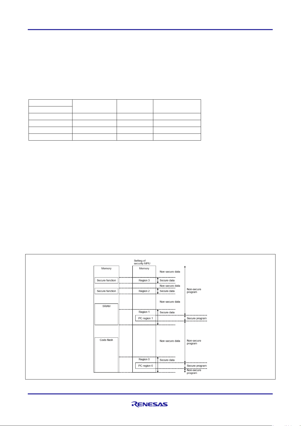
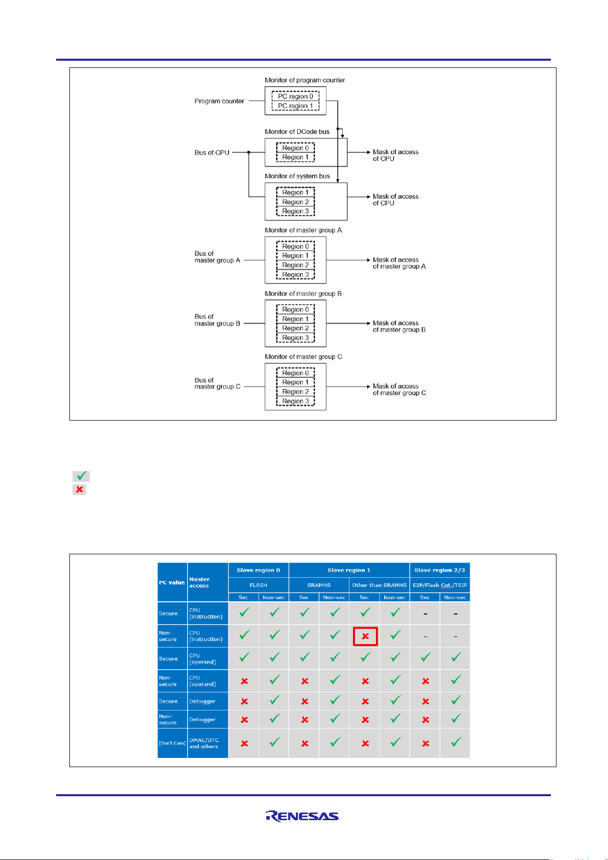
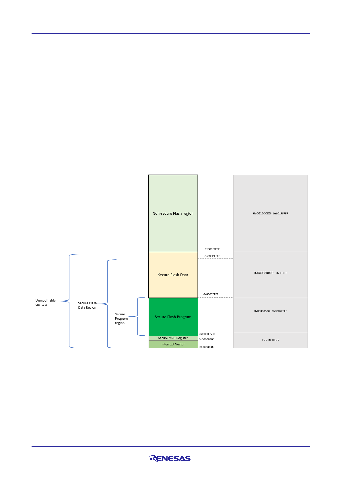
2.2.1 Secure Data Regions
Figure 1 describes the available secure data regions and secure program regions provided by the Security
MPU. Each region is defined by a pair of start and end addresses and an enable bit.
R11AN0416EU0130 Rev.1.30 Page 7 of 46
Dec.15.20
Figure 1. Security MPU Secure Regions
Page 8
Renesas RA Family Securing Data at Rest Utilizing the Renesas Security MPU
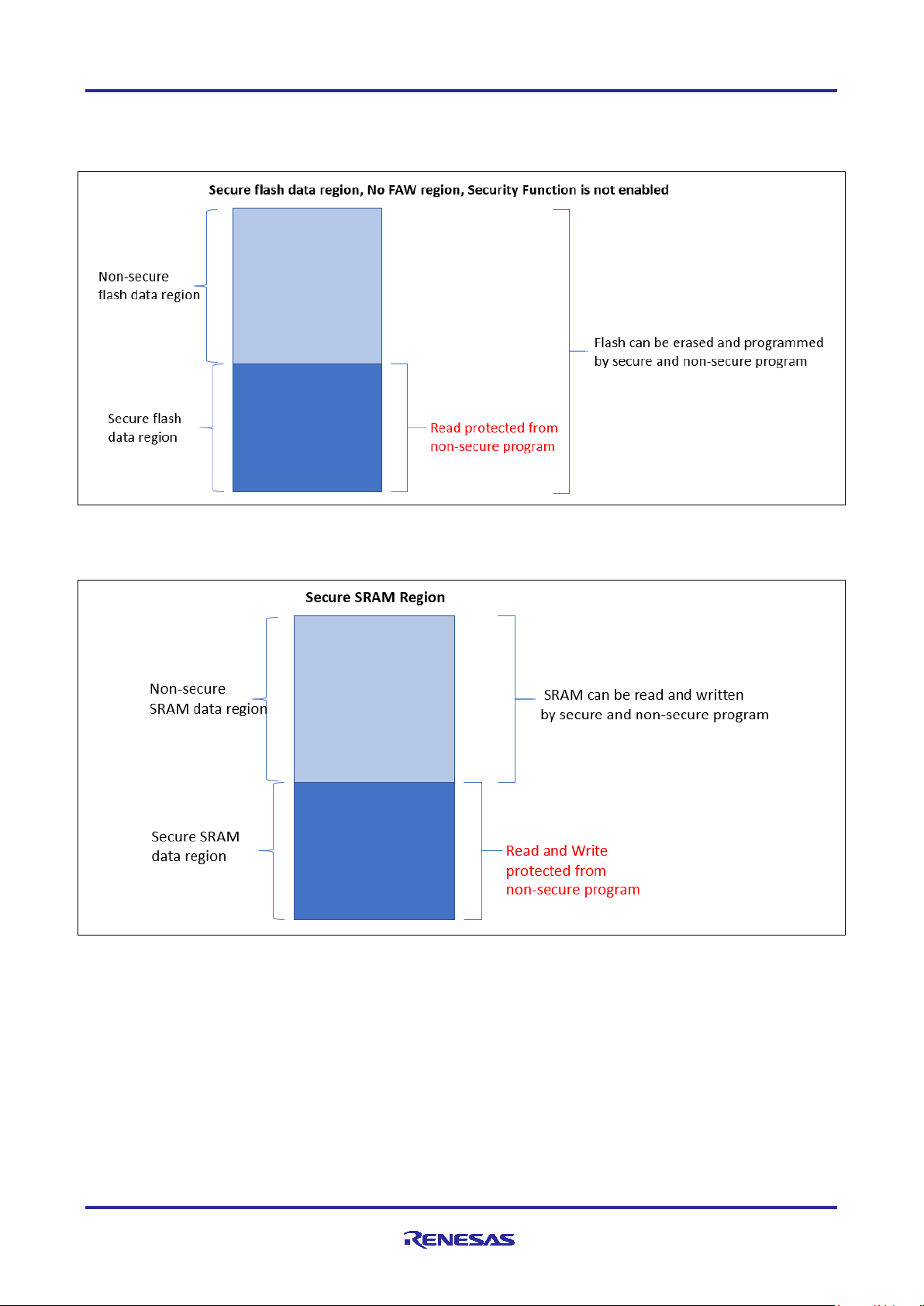
The Security MPU provides four secure data regions, as shown in Figure 1.
• One secure flash data region (located in the MCU’s code flash region). Note that in terms of Security
MPU usage, the secure flash data region can contain both secure flash data and secure flash program.
Figure 2. Secure Flash Data Region
• One secure SRAM data region. Note that in terms of Security MPU usage, secure SRAM data region can
contain both secure SRAM data and secure SRAM program.
Figure 3. Secure SRAM Data Region
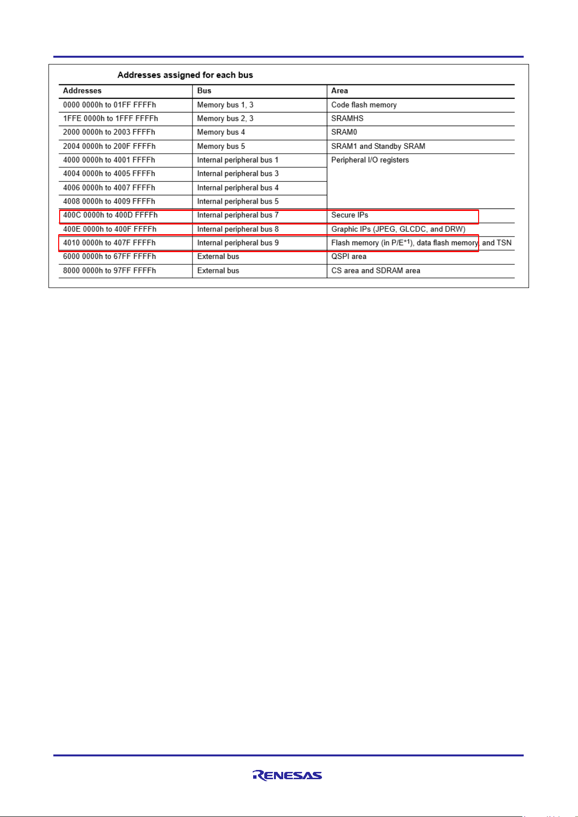
• Two security function regions
Security function region for the SCE (Secure Crypto Engine): address 0x400C0000 to 0x400DFFFF
• This region maps to the RA MCU’s internal peripheral bus 7
• When this security function is enabled, the SCE cannot be controlled from a non-secure program
Security function for the flash (code and data) erase and program (E/P): address 0x40100000 to
0x407FFFFF
• This region maps to the RA MCU’s internal peripheral bus 9
• When this security function is enabled, the flash cannot be put in erase and program mode from a
non-secure program
• Note that this security function does not control TSN even though it is in the same memory space.
R11AN0416EU0130 Rev.1.30 Page 8 of 46
Dec.15.20
Page 9
Renesas RA Family Securing Data at Rest Utilizing the Renesas Security MPU
Figure 4. Security Function Regions
2.2.1.1 Secure Program
The Security MPU provides two secure program regions, each defined by a pair of start and end Program
Counter (PC) addresses and an enable bit. There can be one secure flash program region and one secure
SRAM program region. For security purpose, it is recommended that the secure program regions are located
within the secure flash and secure SRAM data region respectively as shown in Figure 1.
Note: The secure program region can reside outside of the secure flash and secure SRAM region; however,
in this case, there is a security hole. The secure program in Flash and SRAM can be read by nonsecure software.
Non-secure program and secure program can make function calls into each secure and non-secure region,
which provides efficiency in embedded system design.
2.2.1.2 Secure Access Monitor and Protection
• The Security MPU monitors and protects secure flash and secure SRAM data regions (Region 0 and
Region 1) from unauthorized CPU read from the D Code bus (Data access), as shown in Figure 5. The
I Code bus (Instruction access) is not monitored. This allows secure instructions to be accessed by the
non-secure program.
• The Security MPU monitors and protects secure SRAM data and security function regions from system
bus access (such as debugger access), as shown in Figure 5.
• The Security MPU monitors and protects all four secure data regions from access from the three bus
master groups. See the hardwar e user’s manual for definition of the bus master groups.
R11AN0416EU0130 Rev.1.30 Page 9 of 46
Dec.15.20
Page 10
Renesas RA Family Securing Data at Rest Utilizing the Renesas Security MPU
Figure 5. Data Protection for Security MPU Regions
The table in Figure 6 describes the details of CPU access and debugger access to the secure and nonsecure regions.
• indicates that the bus master on the left is granted access to the region on the top
• indicates that the bus master on the left is not granted access to the region on the top
Note: The secure program located in the SRAM region other than the SRAMHS region cannot be fetched by
a non-secure program as marked by the red box shown in Figure 6.
Configuration details of the Security MPU are described in section 3.2.
Figure 6. CPU and Debugger Access Summary
R11AN0416EU0130 Rev.1.30 Page 10 of 46
Dec.15.20
Page 11
Renesas RA Family Securing Data at Rest Utilizing the Renesas Security MPU
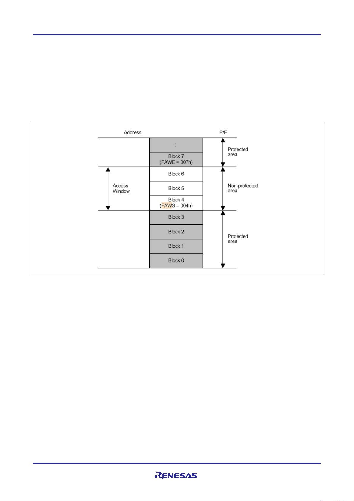
2.3 Flash Access Window (FAW)
The Flash Access Window (FAW) defines one contiguous flash region within the MCU flash space. Within
this region, the flash erase and write operation is allowed from both secure and non-secure program. The
access window is only valid in the program flash area. The access window provides protection in selfprogramming mode, serial programming mode, and on-chip debug mode.
The FAW region setting uses flash block boundaries as the start and end addresses of the flash access
window. There is one bit (FSPR bit) in the FAW control register that, when cleared, disables any possible
update to the flash access window setting for the lifetime of the device. The internal flash write-once
protection uses this bit to implement the write-once protection.
Refer to section 3.3 for configuration details on the FAW.
Figure 7. Flash Access Window
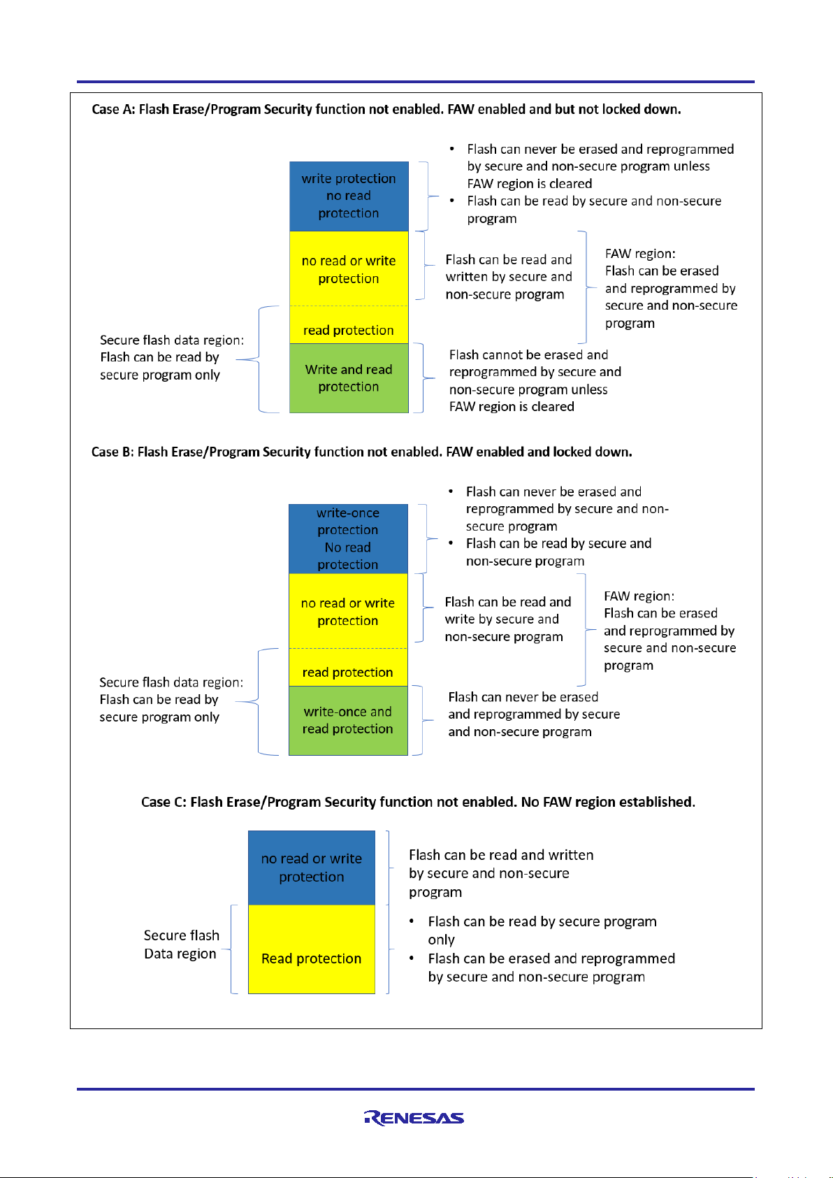
2.3.1 Using the Security MPU and FAW for Code Flash Write Protection
As explained in section 1.2.2, there are two ways to establish flash region write protection. In this application
project, the FAW is used to establish flash write protection. Figure 8 summarizes the code flash read, erase
and programming access control when the Security MPU is used in conjunction with the FAW, and the
security function is not enabled.
R11AN0416EU0130 Rev.1.30 Page 11 of 46
Dec.15.20
Page 12
Renesas RA Family Securing Data at Rest Utilizing the Renesas Security MPU
Figure 8. Code Flash Read, Erase, and Program Control when Security Function is not Enabled
R11AN0416EU0130 Rev.1.30 Page 12 of 46
Dec.15.20
Page 13

Renesas RA Family Securing Data at Rest Utilizing the Renesas Security MPU
2.4 Debugging Security Considerations
The RA MCUs provide OCD/serial programmer ID code protection with the OSIS register. The OSIS register
stores the ID for ID code protection of the OCD/serial programmer. Once the OSIS register ID code is set for
the MCU, the user must provide the matching ID code when connecting an OCD/serial programmer. If the
ID code matches, debugging is allowed; otherwise, the debugging process is not allowed. Configuration of
the OSIS ID code protection is described in section 3.5.
2.5 Notes on Arm MPU, Bus Master MPU, Bus Slave MPU
This section explains how the MPU, Bus Master MPU, and Bus Slave MPU relate to Data at Rest design.
Refer to the Arm
Refer to RA MCUs hardware user’s manuals to understand the definition and settings of the Bus Master and
Bus Slave MPUs.
While these three MPUs intend to catch inadvertent accesses to the regions defined by these MPUs, they do
not provide protection of reading and updating the register settings from non-secure program. The register
settings of these MPUs are not protected from reading by a debugger nor by non-secure programs. Secure
and non-secure programs can follow correct procedures to update the registers.
In addition, the MPU regions defined by these three MPUs do not provide the same level of security
compared to the protection prov ide d by the Security M PU:
• A debugger can access the protected regions
• A read-protected region (without write protection) can be written by secure and non-secure code
• A write-protected region (without read protection) can be read by secure and non-secure code
• A read/write-protected region cannot be read nor written by either secure or non-secure code
®
Cortex technical user manual to understand the definition and settings of the Arm MPU.
2.6 Other Security Elements
2.6.1 Secure Crypto Engine (SCE)
The Secure Crypto Engine (SCE) hardware block on RA MCUs provides data encryption and authentication
capability. Following are the encryption and authentication algorithms supported.
2.6.1.1 Security Algorithms
• Symmetric algorithms: AES
• Asymmetric algorithms: RSA and ECC
• MCU support status:
RA6M3, RA6M2, and RA6M1 MCU Groups support all the above symmetric and asymmetric
algorithms
RA4M1, RA4W1, and RA2A1 support only symmetric algorithms
Configuration details of the SCE is outside the scope of this application project. Refer to the hardware user
manual and FSP user manual for operational details.
2.6.1.2 Other Crypto Security Features
• TRNG (True Random Number Generator)
• Hash value generation: SH A1, SH A22 4, SHA 256 , GH ASH
• 128-bit unique ID
• MCU support:
RA6M3, RA6M2, and RA6M1 support this entire group of features
RA4M1, RA4W1 supports AES, TRNG and GHASH
RA2A1 supports AES and TRNG.
R11AN0416EU0130 Rev.1.30 Page 13 of 46
Dec.15.20
Page 14
Renesas RA Family Securing Data at Rest Utilizing the Renesas Security MPU
3. Configuring the Security Elements
This section explains the detailed process to setup the Security MPU, FAW, and the OSIS ID register to
provide the desired security level for Data at Rest security design. It also explains how to undo the security
feature settings in the development stage. In addition, steps needed to lock the security features in the MCU
are provided.
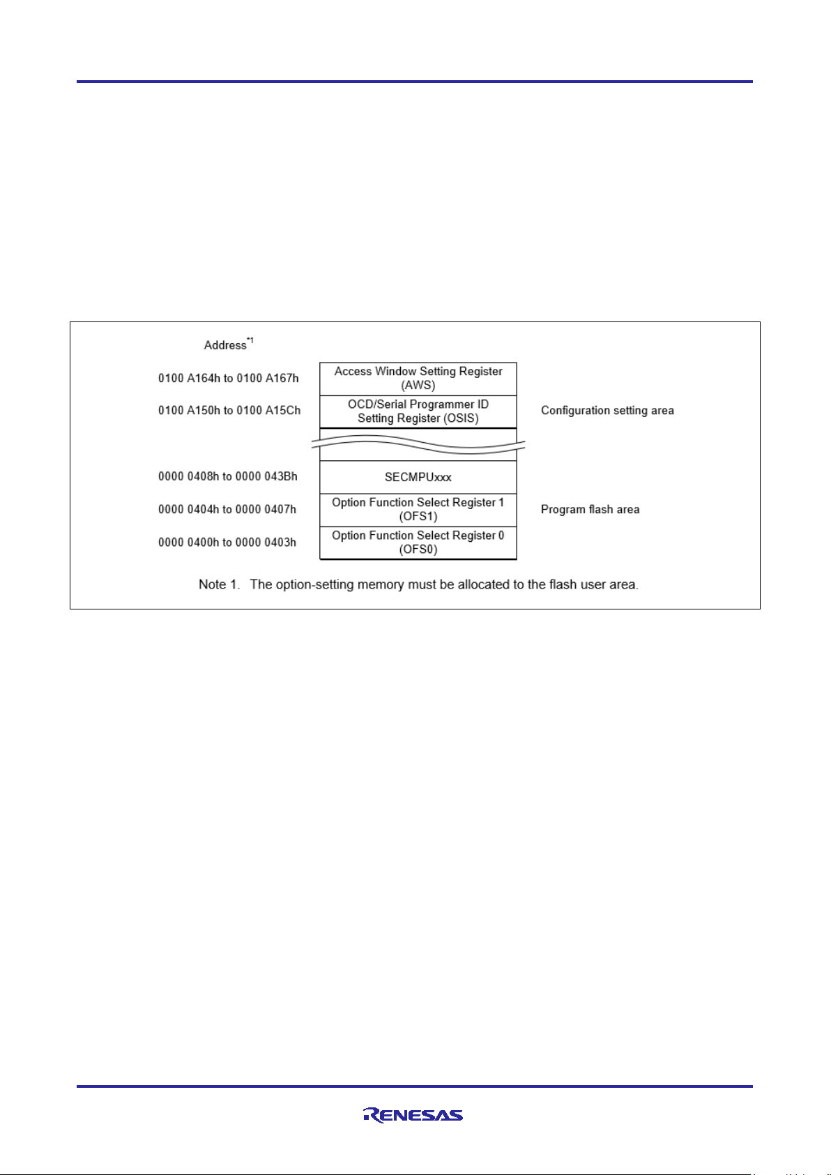
3.1 Overview of RA MCU Option-Setting Memory
The Security MPU and the FAW registers are in the MCU Option-Setting Memory, as shown below. The
option-setting memory is in the flash user area. Setting these registers requires different procedures
compared to erasing and programming the other part of the code and data flash area. Figure 9 is an
example location of the option-setting mem or y based o n RA6M3. Other MCUs can have the FAW register
located at a different loc at io n. Refer to the hardware user’s manual for the exact location for the MCU
involved.
Figure 9. Option-setting Memory Area
As we can see from Figure 9, the Security MPU registers are allocated in the first sector of the program flash
area. The FAW register and OSIS register settings are allocated in the configuration setting area.
With FSP 0.8 or lower, we recommend using the following methods to set up the Security MPU and FAW
registers:
• Use the RA MCU configurator to define the Security MPU registers. Section 3.2.1 describes this method.
• Use the FSP flash driver API to configure the FAW register when locking the register settings is not
required. Use the factory bootloader to lock the FAW register setting. Section 3.3 describes this method.
Other methods of setting the Security MPU and FAW registers include the following:
• Use a J-Link script.
• Use a serial port to communicate with the MCU’s factory bootloader and use the factory bootloader’s
utilities (section 3.4 describes using this method to clear the locking bit, FSPR and hence permanently
lock the FAW register setting).
R11AN0416EU0130 Rev.1.30 Page 14 of 46
Dec.15.20
Page 15
Renesas RA Family Securing Data at Rest Utilizing the Renesas Security MPU
3.2 Configuring the Security MPU
This section describes the steps needed to set up and reset the Security MPU registers.
3.2.1 Setting up the Security MPU Registers
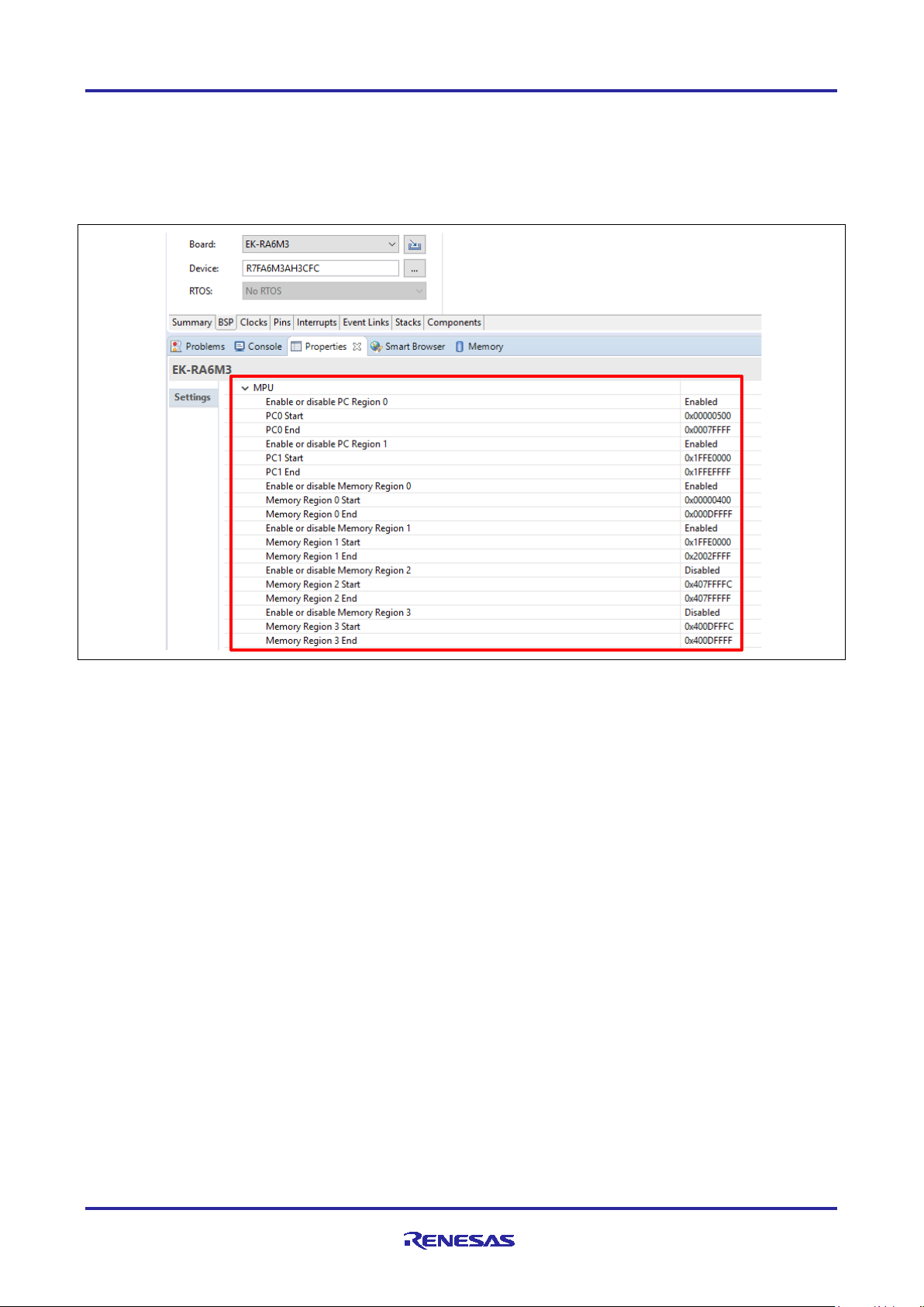
Through the RA MCU configurator FSP BSP tab, users can define and enable the four secure data regions
and the two secure program regions.
Figure 10. Security MPU Configuration
The following list describes all the regions defined by the above property fields (in bold).
• Secure flash program
PC0 Start and PC0 End: program counter region for the secure flash program
Enable or disable PC Region 0: enable or disable the secure flash program
• Secure SRAM program
PC1 Start and PC1 End: program counter region for the secure SRAM program
Enable or disable PC Region 1: enable or disable the secure SRAM program
• Secure flash data region
Memory Region 0 Start and Memory Region 0 End: secure flash data region start and end
addresses
Enable or disable Memory Region 0: enable or disable the secure flash data region
• Secure SRAM data region
Memory Region 1 Start and Memory Region 1 End: secure SRAM data region start and end
addresses
Enable or disable Memory Region 1: enable or disable the secure SRAM data region
• Security Function Region 1
Memory Region 2 Start and Memory Region 2 End: security function 1 start and end addresses
(must be the address space for internal peripheral bus 7 or 9, see description that follows)
Enable or disable Memory Region 2: enable or disable the security function 1
• Security Function Region 2
Memory Region 3 Start and Memory Region 3 End: security function 2 start and end addresses
(must be the address space for internal peripheral bus 7 or 9, see description that follows)
Enable or disable Memory Region 3: enable or disable security function 2
See section 4.1 for the operational flow of using the Security MPU in an application project.
R11AN0416EU0130 Rev.1.30 Page 15 of 46
Dec.15.20
Page 16

Renesas RA Family Securing Data at Rest Utilizing the Renesas Security MPU
3.2.2 Locating Secure Code/Data to a Specific Memory Region
In addition to setting up the Security MPU registers, one must allocate the secure code and secure data to
the intended memory region. This is achieved by customizing the linker script. When you have regions of
secure and non-secure program, the default linker is not sufficient. When designing with the Security MPU,
you must define multiple flash and/or SRAM regions in the linker script.
Refer to section 5.1.2 for an example of locating secure code/data to a specific memory region.
3.2.3 Resetting the Security MPU registers
Resetting the Security MPU registers is possible if the Security MPU registers are located in the FAW region,
or if they are located outside the FAW region, but the FAW region is not permanently locked down.
Resetting the Security MPU requires a flash erase operation for the first block of the MCU flash. Be low are
the steps to reset the Security MPU setting with a RA MCU e2 studio project:
1. Create an SRAM project to execute from an SRAM region other than SRAMHS.
2. Open the flash HAL driver.
3. If the Security MPU flash region is not part of the FAW region, clear the FAW register setting first. See
section 3.3.2 to understand how to clear the FAW region.
4. Erase the first flash block using the flash HAL driver.
5. Close the flash HAL driver.
Reference the example e
the implementation of these steps.
2
studio project secure_data_at_rest_ek_ra6m3 described in section 5.2 for
3.3 Configuring the FAW
This section describes the steps to set up and clear the FAW regions, and to permanently lock the FAW
setting.
3.3.1 Setting up the FAW Region
Call the following FSP FAW API to set up the FAW:
err = R_FLASH_HP_AccessWindowSet(&g_flash0_ctrl, FAW_START, FAW_END);
where,
• g_flash0_ctrl is the instance of this flash HAL driver.
• FAW_START is the start address of the FAW window.
• FAW_END is the address of the next block acceptable for programming and erasure defined by the access
window.
Note: This API always intends to disable the FAW locking. If the FAW is permanently locked prior to running
this API, this API will NOT function as expected, the FAW region cannot be updated anymore.
3.3.2 Clearing the FAW Regions
Call the following FSP FAW API to clear the FAW setting:
err = R_FLASH_HP_AccessWindowClear(g_flash0.p_ctrl);
The R_FLASH_HP_AccessWindowClear API clears the FAW window setting, essentially disabling the
FAW control by setting the start address and end address to 0. This routine will work only if the FAW is not
permanently locked.
Follow the steps below to clear the FAW setting in the development stage (prior to clear FSPR) in a RA MCU
2
studio project:
e
1. Create an SRAM project to execute from an SRAM region other than SRAMHS.
2. Open the flash HAL driver.
3. Clear the FAW setting using R_FLASH_HP_AccessWindowClear.
4. Close the flash HAL drive.
R11AN0416EU0130 Rev.1.30 Page 16 of 46
Dec.15.20
Page 17

Renesas RA Family Securing Data at Rest Utilizing the Renesas Security MPU
3.4 Per m anent Locking of the FAW Region
Permanently locking the FAW region prevents a user from updating the FAW region. This step is needed to
establish the write-once flash region.
There are two use cases when a user may want to consider permanently locking the FAW region:
1. To lock critical runtime data in real time when the device is deployed to the field (the use case without
secure bootloader).
2. To lock critical data/code during the manufacturing stage (the use case with secure bootloader).
FSP 0.8 or earlier does not support the first use case.
For manufacturing usage, to permanently lock the FAW register, we can use the factory bootloader routines,
which implement the FAW register setting and clearing procedure. This application project provides an
example PC application final_program_installer to program the application and permanently lock the
FAW.
Figure 11. Permanently Locking the FAW
3.5 Setting up the Security Control for Debugging
The OCD/Serial Programming ID Setting Register (OSIS) stores the ID code protection for the OCD/serial
programmer. Upon connection, an OCD/serial programmer must provide an ID value so that the MCU can
determine whether to permit the connection.
Following are the brief rules to set up the ID Code. Refer to the hardware user’s manual for details.
• OSIS
128-bit register holds the ID for authenticating the debugger/programmer.
SCI/USB boot mode programming also uses this ID code.
• Bit [127] = 0 totally disables the debug and factory programming
• Bit [126] = 1 allows the debug and factory programming on ID code match
The flash is erased on connecting in factory programming mode.
If the FAW window is permanently locked, the flash cannot be erased.
If the Security MPU is enabled for the flash block, the Factory Bootloader is disabled.
• Bit [126] = 0 allows debug and factory programming on ID code match.
There are multiple ways the user can set up the OSIS ID code:
• Use the RA MCU Configurator with the support of the J-Link debugger
• Use Renesas Flash Programming Tool (RFP)
See the Reference section for the RFP down lo ad link .
• Use a J-Link script
• Use the factory bootloader
• Use the flash HAL driver to program the OSIS ID
R11AN0416EU0130 Rev.1.30 Page 17 of 46
Dec.15.20
Page 18

Renesas RA Family Securing Data at Rest Utilizing the Renesas Security MPU
3.5.1 Methods of Setting the OSIS ID Code
3.5.1.1 Using the RA MCU Configurator and J-Link Debugger
The RA MCU configurator allows the user to set up the OSIS ID code through the FSP property setting
shown in Figure 12.
Figure 12. Setting up OSIS ID using RA MCU Configurator
• During development stage, it is recommended to choose “Locked with All Erase support” for the ID Code
Mode selection. Section 5.5 provides an example a J-Link script which erases the entire flash to reset the
ID code setting to all FFs.
• When “Locked” is selected for the ID Code Mode, the device will be disabled from debugging and factory
programming.
3.5.1.2 Using a J-Link script
The J-Link script SEGGER can setup the OSIS ID. This application project does not provide an example script
for this usage.
3.5.1.3 Using the factory bootloader
The factory bootloader has capability of setting up the OSIS ID. This application project does not provide an
example for this functionality.
3.5.1.4 Using the flash driver
FSP 0.8 or later has the capability of setting up the OSIS ID using the flash driver.
err = R_FLASH_HP_IdCodeSet(&g_flash0_ctrl, id_bytes, FLASH_ID_CODE_MODE );
• g_flash0_ctrl is the instance of this flash HAL driver.
• Id_bytes is the ID code to set.
• FLASH_ID_CODE_MODE has three options:
FLASH_ID_CODE_MODE_UNLOCKED: ID code is ignored;
FLASH_ID_CODE_MODE_LOCKED_WITH_ALL_ERASE_SUPPORT: ID code is checked. All erase is
available;
FLASH_ID_CODE_MODE_LOCKED: ID code is checked.
This application project does not provide an example using this API.
R11AN0416EU0130 Rev.1.30 Page 18 of 46
Dec.15.20
Page 19

Renesas RA Family Securing Data at Rest Utilizing the Renesas Security MPU
3.5.2 Method of Setting up the OSIS ID Code for Debugging
With e2 studio, a user can set up the ID code using this interface.
Figure 13. Setting up the ID Code with e2 studio
3.5.3 Method of Resetting the OSIS ID code
Following are the methods of resetting the OSIS ID code.
3.5.3.1 Using J-Link script
This application project includes an example J-Link script to reset the OSIS ID code by erasing the entire
flash. Refer to section 5.5 for details on the operation.
3.5.3.2 Using factory bootloader
User can use the RFP routine to reset the OSIS ID.
3.5.3.3 Self-programming
Supported by FSP Flash driver.
4. Operational Flow using Security MPU and FAW
This section describes the operational flow for designing a secure application using the RA MCU Security
MPU and FAW.
4.1 Internal Flash and SRAM Read Protection
When the Security MPU enables the secure flash data and secure SRAM data regions, these regions gain
read protection:
• Secure SRAM regions are read and write protected from non-secure flash and SRAM programs
• Secure flash regions are read protected from non-secure flash and non-secure SRAM programs
• The bus master and debuggers are disabled from access to the secure region
The high-level operational flow of establishing the Security MPU regions is described by the flow diagram in
Figure 14. Reference Figure 8 for examples of internal flash read protection.
R11AN0416EU0130 Rev.1.30 Page 19 of 46
Dec.15.20
Page 20

Renesas RA Family Securing Data at Rest Utilizing the Renesas Security MPU
Figure 14. Operational Flow for Using the Security MPU
The following is a summary of setting up the Security MPU for the MCU:
• Use the configurator BSP tab to define secure regions
• Use the linker script to define the secure regions and non-secure regions
• Establish the secure and non-secure functions
• Copy the secure SRAM function (if defined) from the secure flash region to the secure SRAM region
• Test the system.
Note: Once the Security MPU is enabled, the MCU needs to run the reset routine (refer to section 5.2)
whenever a new program needs to be programmed on the device.
4.2 Internal Flash Write Protection
As described in section 4.1, the internal SRAM region gains write protection when the Security MPU is
enabled for the secure SRAM region. The internal flash region can gain write protection through two
methods:
• Set up the FAW region such that it does not include the secure flash region. The entire region (whether it
is part of the secure flash region or non-secure flash region) that is not included in the FAW region will
have erase and write protection from secure and non-secure program. Reference Figure 8 for an
example of internal flash write protection.
• When the Security Function for internal peripheral bus 9 is enabled, the entire flash region, including
secure and non-secure flash regions, is protected from erasing and programming by non-secure flash
and non-secure SRAM program.
In this application project, only the first method is described. See section 5.1 for an example of the
implementation.
R11AN0416EU0130 Rev.1.30 Page 20 of 46
Dec.15.20
Page 21

Renesas RA Family Securing Data at Rest Utilizing the Renesas Security MPU
4.2.1 Operational Flow
The FSP API, R_FLASH_HP_AccessWindowSet (see section 3.3.1) must be called from the user
application to set up the erase and write enabled region. The rest of the flash region will be disabled for
erase and write from both secure and non-secure programs.
Figure 15. Establish Write Protected Internal Flash Region
4.3 Internal Flash and SRAM Read/Write Protection
When the Security MPU is enabled for the secure SRAM region, the secure SRAM gains read/write
protection from non-s ec ure flas h and non-secure SRAM programs.
If the write-protected flash region is part of the secure flash region, this secure flash region is read and write
protected from non-secure program and write protected from secure program. Reference Figure 8 for an
example of internal flash read and write protection.
4.3.1 Operational Flow
When the internal SRAM region gains read protection by setting up the secure SRAM region, it also gains
write protection by the same process. Refer to section 4.1 for details on the operational flow.
If the write protected internal flash region is set up through the FAW, and it is also part of the secure flash
data region, this section of the secure flash region is erase and write protected from the secure and nonsecure programs. The entire secure flash region is read protected from the non-secure program.
Refer to section 5.1 for an example of the implementation of internal SRAM and flash read and write
protection.
Figure 16. Establish Read/write Protected Internal Flash Region
R11AN0416EU0130 Rev.1.30 Page 21 of 46
Dec.15.20
Page 22

Renesas RA Family Securing Data at Rest Utilizing the Renesas Security MPU
4.4 Internal Flash Write-Once Protection
When the FSPR bit is cleared in the FAW register, the intern al fl as h region which is not included in the FAW
window becomes write-once protected from the secure and non-secure programs. The content within this
write-once protected region cannot be altered for the lifetime of the device. Reference Figure 8 for an
example of the internal flash write-once protection.
4.4.1 Operational Flow
Before performing the write-once protection:
• Fully test the critical data and/or code which the application intends to lock down
• Ensure that no other critical data and/or code need to be assigned to the write-once protected region
Figure 17 is the operational flow when operating in a manufacturing stage. Refer to section 5.3 for an
implementation of the write-once protection.
Figure 17. Write-once Protection
As explained in section 3.4, runtime write-once protection by locking the FAW register is not supported by
FSP 0.8 or earlier.
4.5 Internal Flash Write-Once and Read Protection
The write-once and read protection can be achieved for secure flash program and data. When a secure flash
region gains read/write protection by setting up the Security MPU and FAW region, a user can permanently
lock the FAW window such that the corresponding region can never be erased and programmed by any
tools, and it is read protected from non-secure software. Erasing and programming this flash region is not
possible via the factory boot loader, J-Link script, or self-programming.
Region 8 in Figure 8 is an example of write-once and read protected internal flash region.
4.5.1 Operational Flow
For internal secure flash applications, a user can follow these operational steps to set up regions that are
write-once from secure and non-secure program and read protected from non-secure program.
Figure 18. Write-once and Read Protection
Refer to section 5.3 for an ex amp le imple men tat ion of loc king down the FAW region.
R11AN0416EU0130 Rev.1.30 Page 22 of 46
Dec.15.20
Page 23

Renesas RA Family Securing Data at Rest Utilizing the Renesas Security MPU
4.6 Oper ation Notes
4.6.1 Memory Allocation
4.6.1.1 Space between Secure and Non-secure Instructions
An address space of greater than 12 bytes is required between the last instruction of a non-sec ure pr ogram
and the first instruction of a secure program. If a secure program is stored the area following the non-secure
program without the gap, the secure program might be fetched as non-secure program. See hardware user
manual for details.
4.6.1.2 Do Not Assign the Memory Mirror Region to the Secure Region
Setting of the memory mirror space (for example, 0200 0000h to 027F FFFFh for RA6M3) for secure region
is prohibited.
4.6.1.3 Startup Area of Security MPU Regions
The start address area of the secure flash data region cannot be set at the vector table area.
The start address of the secure SRAM data region cannot be set at the stack area or the vector table area.
4.6.2 Limitations on Programming the Option-Setting Memory
Refer to the hardware user manual section “Changing the option-setting memory by self-programming” and
“Debugging through an OCD or programming by a flash writer “to understand the limitations on programming
the Option-Setting Memory for flash access window setup and OSIS ID setup.
The application code included in this application project follows the guidelines provided in the user manual.
4.6.3 Factory Bootloader Accessibility
If the Security MPU is enabled, the factory bootloader is not available anymore. Reset of the Security MPU
register settings is needed to re-enable the factory bootloader. Refer to section 5.2 for a Security MPU reset
example implementation.
4.6.4 Access Secure Function from Non-Secure Functions
Secure functions can be called from non-secure functions (see Figure 6 in 2.2).
The application project implemented in this release calls the secure function directly from the non-secure
function.
Special considerations are needed when accessing secure functions located in a secure bootloader:
• Define a group of secure function entry points (function pointers) in the secure flash data region
• Access the secure function from a function pointer stored in the secure function table
4.6.5 Debugger Access to the Security MPU Regions
When the debugger is operating in debug mode, viewing of the Security MPU flash and secure SRAM region
contents are disabled. With e
are shown as “0”.
2
studio, when the secure region is viewed from the ‘memory’ view, the values
5. Security Application e2 studio Projects: Internal Flash and SRAM
This section introduces the example projects for using the Security MPU and FAW as follows:
• Access secure flash and secure SRAM data from secure flash and secure SRAM code
• Access secure flash and secure SRAM data from non-secure flash
There are three example projects included for the internal flash and SRAM secure Data at Rest application:
R11AN0416EU0130 Rev.1.30 Page 23 of 46
Dec.15.20
Page 24

Renesas RA Family Securing Data at Rest Utilizing the Renesas Security MPU
• Project 1: e2 studio RA MCU project (\embedded\secure_data_at_rest_ek_ra6m3) that
demonstrates the following:
Secure flash data read protection
Secure and non-secure flash data write protection
Secure SRAM read and write protection
• Project 2: e
following:
Reset of the Security MPU
Reset of the FAW region
• Project 3: PC-based Visual Studio application (programInstaller.sln) that downloads the
application created from project 1 and provides the option to permanently lock the FAW via the factory
bootloader on the MCU, thus realizing the write-once protection of the regions not included in the FAW.
In addition, there are several example J-Link scripts included in this application project, which performs the
Security MPU, FAW, and OSIS ID code resetting.
Section 5.4 explains a J-Link script that resets the FAW and Security MPU registers before the FAW region
is permanently locked down.
Section 5.5 explains the procedures for setting up the OSIS ID with an e
project and the usage of the J-Link scripts to reset the OSIS ID. The reset OSIS ID script is used in
conjunction with the blinky project to demonstrate an end-to-end development for debugging security
handling with the RA MCUs using FSP 0.8.
2
studio RA MCU project (\embedded\reset_flash_pk_ra6m3) that demonstrates the
2
studio auto generated blinky
5.1 Project 1: e2 studio project - Internal Flash and SRAM Read Write Protection
5.1.1 Software Architecture Overview
Project 1: This project implements four groups of the software components that demonstrate the flash and
SRAM read and write protection.
• J-Link RTT Viewer User Interface code
• Secure flash code
• Secure SRAM code
• Non-secure flash code
The J-Link RTT user code runs in the non-secure flash region. It monitors user input from the J-Link RTT
Viewer and activates the corresponding secure flash/SRAM and non-secure flash application code. See
Figure 19.
Figure 19. Project 1 Software Block Diagram
R11AN0416EU0130 Rev.1.30 Page 24 of 46
Dec.15.20
Page 25
Renesas RA Family Securing Data at Rest Utilizing the Renesas Security MPU
5.1.2 Memory Allocation Arrangement
The SRAM and Flash memory regions of the system is controlled by the linker script
\secure_data_at_rest_ek_ra6m3\script\ra6m3.ld.
The Security MPU regions are defined by the configuration settings under the BSP tab in the RA Smart
Configurator as shown Figure 10. Security MPU Configuration.
The FAW region is defined by below two macros \src\ DAR_utilities.h.
• #define FAW_START (0x100000)
• #define FAW_END (0x1FFFFF)
It is important to note that the RTT Viewer message output included in this application project is based on the
default project settings for the SRAM, Flash memory regions, Security MPU regions and default FAW setting
as shown below. If these configurations are changed, different outputs are expected. These are not covered
in the provided screen shots as the result varies based on the configurations.
The software uses macros defined in secure_definitions.h to allocate the different secure and nonsecure code.
Figure 20 shows the flash memory allocation based on the flash software components.
Figure 20. Project 1 Internal Flash
In this example project, the FAW window does not include any Secure MPU defined secure flash region. By
setting up the FAW window like this, the Security MPU Registers as well as the secure flash data region is
protected from modification from both secure and non-secure code.
If user wishes to have a portion of the secure flash data region inside the FAW window, they can update the
FAW_START macro definition to adjust the FAW window location.
Note that it is always recommended to exclude the Secure MPU Register settings outside the FAW window,
so the Security MPU settings can be protected from modification and thus enhance the security of the
system.
R11AN0416EU0130 Rev.1.30 Page 25 of 46
Dec.15.20
Page 26

Renesas RA Family Securing Data at Rest Utilizing the Renesas Security MPU
Figure 21 shows the SRAM memory allocation based on the different SRAM software components.
Figure 21. Project 1 Internal SRAM
Following are the memory regions defined by the linker script (\script\ra6m3.ld):
/* Linker script to configure memory regions. */
MEMORY
{
VECTOR_TABLE (rx) : ORIGIN = 0x00000000, LENGTH = 0x00000400 /*1024 bytes */
SECURE_PROGRAM (rx) : ORIGIN = 0x00000400, LENGTH = 0x0007FC00 /* 512K - 1024 bytes */
SECURE_DATA (rw) : ORIGIN = 0x00080000, LENGTH = 0x00080000 /* 512K bytes */
FLASH (rx) : ORIGIN = 0x00100000, LENGTH = 0x00100000 /* 1MB */
SECURE_RAM_PROGRAM (rwx) : ORIGIN = 0x1FFE0000, LENGTH = 0x00010000 /* 64K */
SECURE_RAM (rw) : ORIGIN = 0x1FFF0000, LENGTH = 0x00040000 /* 256K */
RAM (rwx) : ORIGIN = 0x20030000, LENGTH = 0x00050000 /* 320K */
DATA_FLASH (rx) : ORIGIN = 0x40100000, LENGTH = 0x00008000 /* 32K */
QSPI_FLASH (rx) : ORIGIN = 0x60000000, LENGTH = 0x04000000 /* 64M */
SDRAM (rwx) : ORIGIN = 0x90000000, LENGTH = 0x02000000 /* 32M */
}
Following are the memory assignment macros used by the secure software and data sections defined by
secure_definitions.h:
#define SECURE_PROGRAM __attribute__((section (".secure_text")))
#define SECURE_CONST __attribute__((section (".secure_rodata")))
#define SECURE_DATA __attribute__((section (".secure_data")))
#define SECURE_BSS __attribute__((section (".secure_bss")))
#define SECURE_SRAM_PROGRAM __attribute__((section (".secure_sram_program")))
Following are the test variables that are used to demonstrate the protection on secure flash data and secure
SRAM data.
Global variables are used to allow read and write directly from non-secure program to simulate reading and
writing to the secure data area.
R11AN0416EU0130 Rev.1.30 Page 26 of 46
Dec.15.20
Page 27

Renesas RA Family Securing Data at Rest Utilizing the Renesas Security MPU
Data Type
Global Variable Name
Comment for data type
Comment on functionality
Secure flash data
s_dataConst
Constant
No access function is provided.
valid.
Secure initialized
s_dataInit
Initialized
No access function is provided.
Secure
example
s_dataWritten
Uninitialized
Write to this variable from non-
Table 2. Test Variables
example
SRAM data
example
uninitialized
SRAM data
Access to this variable from
non-secure program is not
Access to this variable from
non-secure program is not
valid.
secure flash program and show
the write is not valid.
5.1.3 Functionality Description
5.1.3.1 J-Link RTT Viewer user interface
This section of code takes user input from the RTT Viewer, activates the operation and then print the test
results on the RTT Viewer.
5.1.3.2 Secure flash program
• Read and write from the secure flash program to the secure SRAM and non-secure SRAM region
Show access to all SRAM regions are granted
• Read from the secure flash program to the secure flash data region and non-secure flash data region
Show access to all flash regions are granted
5.1.3.3 Secure SRAM program
• Read and write from the secure SRAM program to the secure SRAM and non-secure SRAM region
Show access to all SRAM regions are granted
• Read and write from the secure SRAM program to the secure flash and non-secure flash region
Show access to all flash regions are granted
5.1.3.4 Non-secure flash program
• Read and write from the non-secure flash program to the secure SRAM and non-secure SRAM region
Show access to the non-secure SRAM region is granted
Show access to the secure SRAM region is not granted
• Read and write from the non-secure flash program to the secure and non-secure flash region
Show that before the FAW is set up, write access to all flash regions is granted. This is an example of
internal flash read protection (see section 4.1)
Show that after the FAW is set up, write access to the non-FAW region is not granted. This is an
example of internal flash write protection (see section 4.2).
• If this non-FAW region is part of the Security MPU region, this is an example of internal flash read
and write protection (see section 4.3)
If we lock the FAW setting (via clearing the FSPR bit):
• The above flash write-protected region beco mes a writ e-once region (see section 4.4)
• The above flash read/write protected region becomes a write-once and read protected region (see
Special Note on the macro definition for SECURE_PADDING:This macro inserts the gap between secure and
non-secure code execution as requested by the Security MPU arc hitect ur e as described in section
section 4.5)
4.6.1.1.
R11AN0416EU0130 Rev.1.30 Page 27 of 46
Dec.15.20
Page 28

Renesas RA Family Securing Data at Rest Utilizing the Renesas Security MPU
User input callbacks
Non-secure flash program
Secure flash program
Secure SRAM program
RTT Application User Interface
Data at Rest Utility
Figure 22 shows the source files grouped by functionality.
Figure 22. Source Code
Note that the non-secure functions defined in the above source files may call secure subroutines and secure
functions defined above may call non-secure subroutines. Security MPU allows cross domain function calls
between secure and non-secure domain.
Care should be taken such that the secure information is not leaking to non-secure region via the stack area.
Whenever it is possible, design the secure function such that they do not use the stack area to store local
variables.
5.1.4 Establishing and Running Software from Secure SRAM Region
Running secure programs from the secure SRAM region involves the following actions:
• Set up the secure SRAM region from the linker script, as shown in section 5.1.2
• Relocate the secure SRAM application code (.secure_sram_program region) from the secure flash
region to the secure SRAM region in the linker script
• Copy the secure SRAM code from the secure flash region to the secure SRAM region using application
code. Refer to the secure_sram_section_copy function (in secure_flash_functions.c) for
implementation
The .code_in_ram FSP code section relocates the flash writing routine to RAM. In this application
project, we allocated this section of the code in the secure SRAM section as shown above.
R11AN0416EU0130 Rev.1.30 Page 28 of 46
Dec.15.20
Figure 23. Allocate Code to Secure SRA M
Page 29

Renesas RA Family Securing Data at Rest Utilizing the Renesas Security MPU
5.1.5 Importing and Building the Project
Create a new workspace and import the \embedded\secure_data_at_rest_ek_ra6m3 project into e2
studio, build, and run the project.
5.1.6 Hardware Setup
Connect J10 using the micro USB cable to the workstation to provide power and debugging capability using
the on-board debugger.
5.1.7 Verifying the Secure Functionalities
Launch ‘J-Link RTT Viewer’ V6.52b or later.
Figure 24. Launch J-Link RTT Viewer
Select ‘USB’ as connection type. Click on the ‘ ’ button to select ‘R7FA6M3AH’ as the device.
If the host PC has more than one J-Link debugg er connec ted to the PC, set the ‘Serial No’ (by default Serial
No is set to 0).
Click ‘Next’ to establish the connection.
Figure 25. Launch SEGGER RTT Viewer
Step 1: The main menu items are printed on the RTT Viewer Te rminal 0.
Figure 26. Main Menu
R11AN0416EU0130 Rev.1.30 Page 29 of 46
Dec.15.20
Page 30

Renesas RA Family Securing Data at Rest Utilizing the Renesas Security MPU
Step 2: Input ‘1’ on RTT Viewer Terminal 0 and view the default Security MPU and FAW settings (Function
read_secure_settings performs this task).
Figure 27. Security Setting
Step 3: Input ‘2’ on RTT Viewer Terminal 0 to view the secure flash functions (functions running in secure
flash region).
Figure 28. Secure Flash Program Operation Menu
Input ‘a’ to read the secure flash, secure SRAM, non-secure flash, non-secure SRAM region from the secure
flash functions and confirm that read accesses are granted. Function secure_code_read() verifies this
functionality.
Figure 29. Secure Flash Program Read
R11AN0416EU0130 Rev.1.30 Page 30 of 46
Dec.15.20
Page 31

Renesas RA Family Securing Data at Rest Utilizing the Renesas Security MPU
Input ‘b’ to perform writing of the secure SRAM, non-secure SRAM regions from the secure flash functions
and confirm the write accesses are granted. Function secure_code_write() performs this function.
Figure 30. Secure Flash Program Writes
Input ‘c’ to set up the FAW. Figure 31 shows the default FAW region set up by the example project. Input ‘1’
to confirm FAW is set up.
Figure 31. Set up the FAW (from 0x100000 to 0x1FFFFF)
R11AN0416EU0130 Rev.1.30 Page 31 of 46
Dec.15.20
Page 32

Renesas RA Family Securing Data at Rest Utilizing the Renesas Security MPU
Input ‘2’ and then ‘d’ to reset the FAW from secure flash program.
Figure 32. Reset the FAW
Input ‘1’ to confirm the FAW region is disabled.
Figure 33. Confirm FAW is Disabled
Step 4: Input ‘3’ to view the secure SRAM functions (functions running out of the secure SRAM region).
Figure 34. Secure SRAM Program
R11AN0416EU0130 Rev.1.30 Page 32 of 46
Dec.15.20
Page 33

Renesas RA Family Securing Data at Rest Utilizing the Renesas Security MPU
Input ‘g’ to read the secure flash, secure SRAM, non-secure flash, non-secure SRAM region from the secure
SRAM functions and confirm read accesses are granted. Function secure_sram_code_read performs this
function.
Figure 35. Secure SRAM Program Read
Input ‘h’ to write to the secure flash, secure SRAM, non-secure flash, non-secure SRAM regions from the
secure SRAM functions with FAW region enabled from 0x100000 to 0x1FFFFF. Function
secure_sram_code_write performs this function.
Figure 36 Secure SRAM Program Write
R11AN0416EU0130 Rev.1.30 Page 33 of 46
Dec.15.20
Page 34

Renesas RA Family Securing Data at Rest Utilizing the Renesas Security MPU
Step 5: Input ‘r’ then ‘4’ to view the non-secure flash functions (functions running out of non-secure flash
region).
Figure 37. Non-secure Flash Program Functions
Input ‘m’ to read the secure flash, secure SRAM, non-secure flash, non-secure SRAM region from the nonsecure flash functions and confirm that reading secure memory is not valid. Function
non_secure_code_read performs this function.
Figure 38. Read Operation from Non-secure Flash Program
Input ‘n’ to write the secure flash, secure SRAM, non-secure flash, non-secure SRAM regions from nonsecure flash program with FAW region enabled from 0x100000 to 0x1FFFFF and show that secure flash
memory should be protected with FAW to prevent non-secure code writing. Function
non_secure_code_write performs this function.
R11AN0416EU0130 Rev.1.30 Page 34 of 46
Dec.15.20
Page 35

Renesas RA Family Securing Data at Rest Utilizing the Renesas Security MPU
Figure 39. Write Operation from Non-secure Flash Program
Step 6: Input ‘d’ to reset the FAW setting and verify the operation by input ‘1’.
Figure 40. Reset FAW and Confirm FAW is Reset
R11AN0416EU0130 Rev.1.30 Page 35 of 46
Dec.15.20
Page 36

Renesas RA Family Securing Data at Rest Utilizing the Renesas Security MPU
5.1.7.1 Summary of the functionalities provided in this application project:
• Establish read/write protection to the secure flash and secure SRAM regions using Security MPU and
FAW setting.
• Shield secure data from the debugger. For demonstration, try to view the memory of the secure data
region from the debugger, value “0” is presented. The protection from debugger is effective after first
power recycle.
Figure 41. Secure Data Region is not Viewable from Debugger
• Establish a blueprint of how to implement secure flash and secure SRAM regions with read & write
protection of the secure SRAM and secure flash regions.
5.1.8 Migrating to Other RA MCUs
As each MCU group and each MCU within a group may have different internal flash and SRAM size.
Follow these steps to migrate this application:
1. Modify the BSP Security MPU region settings to fit the memory size.
2. Copy over the RA6M3.ld and rename to confirm to the new RA MCU.
3. Modify the linker script to take care of the new secure flash and SRAM regions defined in the BSP tab.
4. Modify the FAW region range if needed in the application code based on the flash size of the new MCU.
5. The entire application code size is about 22kB flash and 5kB of SRAM. Please use these numbers as
reference when migrating to other RA MCU devices. No application code update is needed when
migrating to RA6M1 and RA6M2.
5.2 Project 2: e2 studio Project - Reset the Security MPU and FAW setting
This e2 studio project \embedded\reset_ek_ra6m3 provides an example to reset the Security MPU and
FAW setting using the FSP Flash HAL driver. The user is advised to run this routine every time they update a
project with the Security MPU enabled or load a new project.
• Note that the linker script is updated from the default to assign both program and data section to SRAM.
• Stack pointer and Program counter needs to update to match the new memory layout based on the linker
script.
R11AN0416EU0130 Rev.1.30 Page 36 of 46
Dec.15.20
Page 37

Renesas RA Family Securing Data at Rest Utilizing the Renesas Security MPU
Figure 42. Set up the SP and PC
Figure 43. Flash Driver on r_flash_hp
After these preparations, call the routines in Figure 44 to clear the FAW region setting. Build and run the
project. Pause the project, it should have reached: while(1); after successful flash erase.
Figure 44. Resetting Security MPU and FAW Settings
R11AN0416EU0130 Rev.1.30 Page 37 of 46
Dec.15.20
Page 38

Renesas RA Family Securing Data at Rest Utilizing the Renesas Security MPU
5.3 Project 3: PC Application to Permanently Lock the FAW
The workstation utility that permanently locks the FAW uses the MCU’s factory loader as shown in Figure 11.
Factory Boot Loader Mode:
Connect Jumper J12 to 2 and 3 to enable USB FS Device mode of RA6M3. Connect J12 to PC using the micro
USB cable.
• Connecting jumper J16 and power cycle the board, the RA6M3 boots with the factory bootloader in USB
program mode, which enables you to load a program directly to the internal microcontroller flash through
the USB device interface (CDC Class).
To use this tool, follow the steps below:
Step 1: Exercise the default evaluation content which programs the default program to EK-RA6M3. The
default progamInstaller.exe under \pc program\final_program_installer_script does not lock
down the FAW. It does set up the FAW region.
1. Put the RA MCU in factory bootloader mode.
2. Open the device manager and find the enumerated COM port number for “USB Ser i al Device”.
3. Run the deploy_app.bat fi le and provide the enumer ated COM port number as the argument. See
example output in Figure 45.
C:\MyProjects\RA\Data at Rest Repo\ra_solutions\Data-at-Rest-Dev\pc
program\final_program_installer_script>deploy_app.bat 12
C:\MyProjects\RA\Data at Rest Repo\ra_solutions\iotsg-2712-secure-data-at-rest-dev\pc
program\final_program_installer_script>REM script to download application and setup FAW
C:\MyProjects\RA\Data at Rest Repo\ra_solutions\iotsg-2712-secure-data-at-rest-dev\pc
program\final_program_installer_script>echo off
Parsed SREC file: secure_data_at_rest_ek_ra6m3.srec (0x0..0x103513)
Initialising flash programming connection to port COM12
Established flash programming connection
Disabling flash access window (0x0..0xFFFFFFFF)
Flash access window is now disabled
Erasing flash
Flash erased OK
Writing flash for secure_data_at_rest_ek_ra6m3.srec region (bufferOffset=0x0, 0x103513
bytes)
Flash region written OK
Flash Access Window configured for start=0x100000, end=0x1fffff
Completed OK
Figure 45. Program the Application witho ut Locking the FAW Region (needs update)
Note: Every time before reprogramming the application, the reset routine must be performed successfully.
Step 2: Proceed with locking the FAW region if needed by following steps:
1. Open the Visual Studio project program_installer.sln (\pc
program\final_program_installer_src\pc\apps\programInstaller\programInstaller.
sln).
2. Open the project properties. Under C/C++>Preprocessor, add a Preprocessor definition for
ACTIVATE_THE_FSPR.
R11AN0416EU0130 Rev.1.30 Page 38 of 46
Dec.15.20
Page 39

Renesas RA Family Securing Data at Rest Utilizing the Renesas Security MPU
Figure 46. Set up the FAW Locking
3. Compile Program_Installer project.
If you are using Visual Studio 2017 professional or enterprise version, you will run into following error
message.
Figure 47. Compiling the Program Installer
To resolve this error message, right-click on the project and select Retarget Projects. Then choose the
SDK version you are using. Proceed to compiling.
Figure 48. Retarget the Solution
4. Compile the application Project 1 \embedded\secure_data_at_rest_ek_ra6m3 with ID code
region removed. This is a limitation of this tool. If you do not change
secure_data_at_rest_ek_ra6m3, there is no need to take this action as there is a copy of the
default .srec file included in the script folder.
5. Put the generated secure_data_at_rest_ek_ra6m3.srec and newly built
programInstaller.exe in the same folder as the deploy_app.bat file (\pc
program\final_program_installer_script).
6. Proceed to use the same steps from 1 to 3 in Step 1 in this section to program the final application.
Warning: The unmodifiable flash region will be permanently locked down with the current image (from 0x0
to 0xFFFFF).
R11AN0416EU0130 Rev.1.30 Page 39 of 46
Dec.15.20
Page 40

Renesas RA Family Securing Data at Rest Utilizing the Renesas Security MPU
Writing flash for secure_data_at_rest_ek_ra6m3.srec region (bufferOffset=0x0, 0x10BBE8
bytes)
Flash region written OK
Flash Access Window configured for start=0x100000, end=0x1fffff
Completed OK
Figure 49. Lock the FAW Region
5.4 Example Reset J-Link Script for the Security MPU a nd FAW
In the \reset_scripts folder, there is the Security MPU and FAW region reset J-Link Script under
\smpu_aws_reset_script. This script resets the Security MPU and FAW settings before the FSPR bit is
cleared (that is, the FAW region is permanently locked down). Under \smpu_aws_reset_script, there
are two files (Figure 50).
Figure 50. Security MPU and FAW Reset Script
Open RA6M3_ERASE_SMPU_AWS.bat and update the SEGGER J-Link version to match your J-Link version
by updating the folder name.
Figure 51. Update the SEGGER J-Link Version
The script performs the following functions:
1. Reset the device.
2. Reprogram the Flash Access Window configuration area (0x0100A160 for RA6M3) to all FFs.
3. Reset the device.
4. Erase the first block of code flash.
5. Reset the device.
To run the reset script, put RA6M3 into Normal Boot mode and open a command line window, navigate to
the location of the .bat file, and run the RA6M3_ERASE_SMPU_AWS.bat. The last portion of the output from
running this script is included below:
Normal Boot: Removing jumper J16 and power cycle the board, the RA6M3 st arts execution from inter nal
flash (ROM). This is the normal mode of operation.
R11AN0416EU0130 Rev.1.30 Page 40 of 46
Dec.15.20
Page 41

Renesas RA Family Securing Data at Rest Utilizing the Renesas Security MPU
J-Link Command File read successfully.
Processing script file...
J-Link connection not established yet but required for command.
Connecting to J-Link via USB...O.K.
Firmware: J-Link OB-S124 compiled Feb 23 2017 17:01:55
Hardware version: V1.00
S/N: 831004110
VTref=3.300V
Selecting SWD as current target interface.
Selecting 2000 kHz as target interface speed
Device "R7FA6M3AH" selected.
…… (omitted the middle portion of the output)
Writing AA00 -> 407FE084
00000000 = FFFFFFFF FFFFFFFF FFFFFFFF FFFFFFFF
00000010 = FFFFFFFF FFFFFFFF FFFFFFFF FFFFFFFF
00000020 = FFFFFFFF FFFFFFFF FFFFFFFF FFFFFFFF
00000030 = FFFFFFFF FFFFFFFF FFFFFFFF FFFFFFFF
00000040 = FFFFFFFF FFFFFFFF FFFFFFFF FFFFFFFF
00000050 = FFFFFFFF FFFFFFFF
Unknown command. '?' for help.
Reset delay: 0 ms
Reset type NORMAL: Resets core & peripherals via SYSRESETREQ & VECTRESET bit.
Reset: Halt core after reset via DEMCR.VC_CORERESET.
Reset: Reset device via AIRCR.SYSRESETREQ.
Script processing completed.
C:\MyProjects\RA\Data at Rest Repo\ra_solutions\iotsg-2712-secure-data-at-rest-dev\reset_scripts\smpu_aws_reset_script>pause
Press any key to continue . . .
Figure 52. Running the Security MPU and FAW Reset Script
5.5 J-Link Scripts for Resetting OSIS ID code for RA6M3
Under \reset_scripts\osis_id_resetting_script, there are three files:
• ID_Code_ERASEALL_RA6M3.bat
• IDCode_ALeRASE_RV40_ph2.jlinkscript
• RA6M3_connect.jlink
Follow the steps below to exercise these reset scripts.
Step 1: If you don’t have the SEGGER tools installed, go to https://www.segger.com/downloads/J-Link/
download and stall the latest J-Link software.
Step 2: Create a blinky project using the e2 studio.
R11AN0416EU0130 Rev.1.30 Page 41 of 46
Dec.15.20
and
Page 42

Renesas RA Family Securing Data at Rest Utilizing the Renesas Security MPU
Figure 53. Create a Blinky Project
Step 3: Setup the ID code in the “Property” field under the BSP tab. Note bit 127 and bit 126 are both set to
1.
Figure 54. Setup ID Code in Configurator
Step 4: Click Generate Project Content, and compile the project.
Step 5: Open the debug configuration Debugger>Connection Settings, input the OSIS ID below. Click
Apply>Debug.
Figure 55. Setup Matching ID Code in Debug Configuration
Step 6: Debug the project. If the debugging is happening, it is a proof that the ID code matched up.
Step 7: Stop the project.
The next couple of steps shows how to reset the OSIS ID code using the script included.
Step 8: Open a command prompt and navigate to the folder where you extracted the script files.
Step 9: Set the path to the version of J-Link that you are using for the RA projects:
set PATH=%PATH%;"C:\Program Files (x86)\SEGGER\JLink”
R11AN0416EU0130 Rev.1.30 Page 42 of 46
Dec.15.20
Page 43

Renesas RA Family Securing Data at Rest Utilizing the Renesas Security MPU
Step 10: Run the batch file ID_Code_ERASEALL_RA6M3.bat you should see output similar to the output
below:
Figure 56. Erase Entire Flash and Reset the OSIS ID Code
R11AN0416EU0130 Rev.1.30 Page 43 of 46
Dec.15.20
Page 44

Renesas RA Family Securing Data at Rest Utilizing the Renesas Security MPU
The following two steps confirm the OSIS ID reset is successfully done.
Step 11: Reset the OSIS ID to all FFs in the configurator for the blinky project (see Figure 54) and compile
the project.
Step 12: Reset the OSIS ID for the debugger configuration to all FFs (see Figure 55) and confirm the
debugging works.
6. Secure Data at Rest Next Steps
6.1 Secure Data Encryption and Authentication
A future release of this application project will cover secure data encryption and authentication.
6.2 External Storage Secure Data at Rest
A future release of this application project will cover external storage data encryption and authentication as
well as access control.
6.3 Example using the Security MPU Security Functions
As explained in section 2.2, there are two security functions that can be controlled by the Security MPU.
One security function controls the access to the Secure Crypto Engine (SCE). When this security function is
enabled, only secure program can access the SCE.
The other security function controls the access to the code and data flash Erase and Programming (E/P).
When this security function is enabled, only secure program can perform internal flash E/P.
This application project does not provide an example of using these security functions.
7. References
1. Renesas Flash Programmer: https://www.renesas.com/us/en/products/software-
tools/tools/programmer/renesas-flash-programmer-programming-gui.html#downloads
2. Arm®v7-M Architecture Reference Manual (ARM DDI 0403D)
3. Arm
4. Arm
®
Cortex®-M4 Processor Technical Reference Manual (ARM DDI 0439D)
®
Cortex®-M4 Devices Generic User Guide (ARM DUI 0553A)
R11AN0416EU0130 Rev.1.30 Page 44 of 46
Dec.15.20
Page 45

Renesas RA Family Securing Data at Rest Utilizing the Renesas Security MPU
8. Website and Support
Visit the following URLs to learn about the RA family of microcontrollers, download tools and documentation,
and get support.
EK-RA6M3 Resources renesas.com/ra/ek-ra6m3
RA Product Information renesas.com/ra
Flexible Software Package renesas.com/ra/fsp
RA Product Support Forum renesas.com/ra/forum
Renesas Support renesas.com/support
R11AN0416EU0130 Rev.1.30 Page 45 of 46
Dec.15.20
Page 46

Renesas RA Family Securing Data at Rest Utilizing the Renesas Security MPU
Rev.
Date
Description
Page
Summary
1.00
Oct.04.19
-
First release document
1.10
May 14.20
-
Update to FSP v1.1.0
1.20
July 15.20
-
Update to FSP v1.2.0, title updated
1.30
Dec.15.20
-
Update to FSP v2.2.0
Revision History
R11AN0416EU0130 Rev.1.30 Page 46 of 46
Dec.15.20
Page 47

Corporate Headquarters
Contact information
www.renesas.com
Trademarks
of their respective owners.
Notice
1. Descriptions of circuits, software and other related information in this document are provided only to illustrate the operation of sem iconductor products
and application examples. You are fully responsible for the incorporation or any other use of the circuits, software, and information in the design of your
product or system. Renesas Electronics disclaims any and all liability for any losses and damages incurred by you or third parties arising from the use
of these circuits, software, or information.
2. Renesas Electronics hereby expressly disclaims any warranties against and liability for infringement or any other claims involving patents, copyrights,
or other intellectual pro pe rty rights of third parties, by or arising from the use of Renesas Electronics products or technical information described in this
document, including but not limited to, the product data, drawings, charts, programs, algorithms, and application examples.
3. No license, express, implied or otherwise, is granted hereby under any patents, copyrights or other intellectual property rights of Renesas Electronics
or others.
4. You shall not alter, modify, copy, or reverse engineer any Renesas Electronics product, whether in whole or in part. Renesas Electronics disclaims any
and all liability for any losses or damages incurred by you or third parties arising from such alteration, modification, copying or reverse engineering.
5. Renesas Electronics products are classified according to the following two quali ty grad es: “Sta ndard” and “High Qualit y ”. The intended applications for
each Renesas Electronics product depends on the product’s quality grade, as indicated below.
"Standard": Computers; office equipment; communications equipment; test and measurement equipm e nt ; audi o and visu al equi p m ent ; hom e
"High Quality": Transportation equipment (automobiles, trains, ships, etc.); traffic control (traffic lights); large-scale communication equipment; key
Unless expressly designated as a high reliability product or a product for harsh environments in a Renesas Electronics data sheet or other Renesas
Electronics document, Renesas Electronics products are not intended or authorized for use in products or systems that may pose a direct threat to
human life or bodily injury (artificial life support devices or systems; surgical implantations; etc.), or may cause serious property damage (spac e
system; undersea repeaters; nuclear power control systems; aircraft control systems; key plant systems; military equipment; etc.). Renesas Electronics
disclaims any and all liability for any damages or losses incurred by you or any third parties arising from the use of any Renesas Electronics product
that is inconsistent with any Renesas Electronics data sheet, user’s manual or other Renesas Electronics document.
6. When using Renesas Electronics products, refer to the latest product information (data sheets, user’s manuals, application notes, “General Notes for
Handling and Using Semiconductor Devices” in the reliability handbook, etc.), and ensure that usage conditions are within the ranges specified by
Renesas Electronics with respect to maximum ratings, operating power supply voltage range, heat dissipation characteristics, installation, etc. Renesas
Electronics disclaims any and all liability for any malfunctions, failure or accident arising out of the use of Renesas Electronics products outsi de of such
specified ranges.
7. Although Renesas Electronics endeavors to improve the quality and reliability of Renesas Electronics products, semiconductor products have specific
characteristics, such as the occurrence of failure at a certain rate and malfunctions under certain use conditions. Unless designated as a high reliability
product or a product for harsh environments in a Renesas Electronics data sheet or other Renesas Electronics document, Renesas Electronics
products are not subject to radiation resistance design. You are responsible for implementing safety measures to guard against the possibility of bodily
injury, injury or damage caused by fire, and/or danger to the public in the event of a failure or malfunction of Renesas Electronics products, such as
safety design for hardware and software, including but not limited to redundancy, fire control and malfunction prevention, appropriate treatment for
aging degradation or any other appropriate measures. Because the evaluation of microcomputer software alone is very difficult and impractical, you are
responsible for evaluating the safety of the final products or systems manufactured by you.
8. Please contact a Renesas Electronics sales office for details as to environmental matters such as the environmental compatibility of each Renesas
Electronics product. You are responsible for carefully and sufficiently investigating applicable laws and regulations that regulate the inclusion or use of
controlled substances, including without limitation, the EU RoHS Directive, and using Renesas Electronics products in compliance with all these
applicable laws and regulations. Renesas Electronics disclaims any and all liability for damages or losses occurring as a result of your noncompliance
with applicable laws and regulations.
9. Renesas Electronics products and technologies shall not be used for or incorporated into any products or systems whose manufacture, use, or sale is
prohibited under any applicable domestic or foreign laws or regulations. You shall comply with any applicable export control laws and regulations
promulgated and administered by the governments of any countries asserting jurisdiction over the parties or transactions.
10. It is the responsibility of the buyer or distributor of Renesas Electronics products, or any other party who distributes, disposes of, or otherwise sells or
transfers the product to a third party, to notify such third party in advance of the contents and conditions set forth in this document.
11. This document shall not be reprinte d, r epr od uc e d or dupli c at ed in any form, in whole or in part, without prior written consent of Renesas Electronics.
12. Please contact a Renesas Electronics sales office if you have any questions regarding the information contained in this document or Renesas
Electronics products.
(Note1) “Renesas Electronics” as used in this document means Renesas Electronics Corporation and also includes its directly or indirectly controll ed
(Note2) “Renesas Electronics product(s)” means any product developed or manufactured by or for Renesas Electronics.
subsidiaries.
electronic appliances; machine tools; personal electronic equipment; industrial robots; etc.
financial terminal systems; safety control equipment; etc.
(Rev.4.0-1 November 2017)
TOYOSU FORESIA, 3-2-24 Toyosu,
Koto-ku, Tokyo 135-0061, Japan
Renesas and the Renesas logo are trademarks of Renesas Electronics
Corporation. All trademarks and registered trademarks are the property
For further information on a product, technology, the most up-to-date
version of a document, or your ne are s t sales office, please visit:
www.renesas.com/contact/
.
© 2020 Renesas Electronics Corporation. All rights reserved.
 Loading...