

Page 1
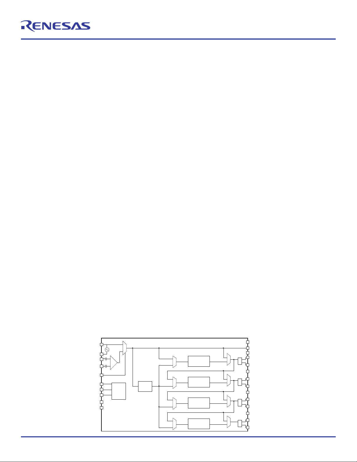
XIN/REF
XOUT
CLKIN
CLKINB
CLKSEL
SD/OE
SEL1/SDA
SEL0/S CL
V
DDA
V
DDD
V
DDO
0
OUT0 _SEL_I 2CB
V
DDO
1
OUT1
OUT1B
V
DDO
2
OUT2
OUT2B
V
DDO
3
OUT3
OUT3B
V
DDO
4
OUT4
OUT4B
FOD1
FOD2
FOD3
FOD4
PLL
OTP
and
Control
Logic
VersaClock® 6E Programmable
Clock Generator
5P49V6965
Datasheet
Description
The 5P49V6965 is a programmable clock generator intended for
high-performance consumer, networking, industrial, computing,
and data-communications applications. Configurations may be
stored in on-chip One-Time Programmable (OTP) memory or
changed using I
2
C interface. This is Renesas’ sixth generation of
programmable clock technology (VersaClock 6E).
The frequencies are generated from a single reference clock. The
reference clock can come from one of the two redundant clock
inputs. A glitchless manual switchover function allows one of the
redundant clocks to be selected during normal operation.
Two select pins allow up to four different configurations to be
programmed and accessible using processor GPIOs or
bootstrapping. The different selections may be used for different
operating modes (full function, partial function, partial
power-down), regional standards (US, Japan, Europe) or system
production margin testing. The device may be configured to use
one of two I
2
C addresses to allow multiple devices to be used in a
system.
Typical Applications
▪ Ethernet switch/router
▪ PCI Express 1.0 / 2.0 / 3.0 / 4.0 Spread Spectrum on
▪ PCI Express 1.0 / 2.0 / 3.0 / 4.0 / 5.0 Spread Spectrum off
▪ Broadcast video/audio timing
▪ Multi-function printer
▪ Processor and FPGA clocking
▪ Any-frequency clock conversion
▪ MSAN/DSLAM/PON
▪ Fiber Channel, SAN
▪ Telecom line cards
▪ Laser distance sensing
Features
▪ Flexible 1.8V, 2.5V, 3.3V power-rails
▪ High-performance, low phase noise PLL, < 0.5ps RMS typical
phase jitter on outputs
▪ Four banks of internal OTP memory
• In-system or factory programmable
• 2 select pins accessible with processor GPIOs or
bootstrapping
2
▪ I
C serial programming interface
• 0xD0 or 0xD4 I2C address options allows multiple devices
configured in a same system
▪ Reference LVCMOS output clock
▪ Four universal output pairs individually configurable:
• Differential (LVPECL, LVDS or HCSL)
• 2 single-ended (2 LVCMOS in-phase or 180 degrees out of
phase)
• I/O V
(LVDS and LVCMOS), 2.5V, or 3.3V
▪ Output frequency ranges:
• LVCMOS clock outputs: 1kHz to 200MHz
• LVDS, LVPECL, HCSL differential clock outputs: 1kHz to
350MHz
▪ Redundant clock inputs with manual switchover
▪ Programmable output enable or power-down mode
▪ Available in 4 × 4 mm 24-VFQFPN package
▪ -40° to +85°C industrial temperature operation
s can be mixed and matched, supporting 1.8V
DD
Block Diagram
1©2020 Renesas Electronics Corporation August 20, 2020
Page 2

5P49V6965 Datasheet
Contents
Description . . . . . . . . . . . . . . . . . . . . . . . . . . . . . . . . . . . . . . . . . . . . . . . . . . . . . . . . . . . . . . . . . . . . . . . . . . . . . . . . . . . . . . . . . . . . . . . . . . . . . . 1
Typical Applications . . . . . . . . . . . . . . . . . . . . . . . . . . . . . . . . . . . . . . . . . . . . . . . . . . . . . . . . . . . . . . . . . . . . . . . . . . . . . . . . . . . . . . . . . . . . . . . 1
Features . . . . . . . . . . . . . . . . . . . . . . . . . . . . . . . . . . . . . . . . . . . . . . . . . . . . . . . . . . . . . . . . . . . . . . . . . . . . . . . . . . . . . . . . . . . . . . . . . . . . . . . . 1
Block Diagram . . . . . . . . . . . . . . . . . . . . . . . . . . . . . . . . . . . . . . . . . . . . . . . . . . . . . . . . . . . . . . . . . . . . . . . . . . . . . . . . . . . . . . . . . . . . . . . . . . . 1
Pin Assignments. . . . . . . . . . . . . . . . . . . . . . . . . . . . . . . . . . . . . . . . . . . . . . . . . . . . . . . . . . . . . . . . . . . . . . . . . . . . . . . . . . . . . . . . . . . . . . . . . . 3
Pin Descriptions . . . . . . . . . . . . . . . . . . . . . . . . . . . . . . . . . . . . . . . . . . . . . . . . . . . . . . . . . . . . . . . . . . . . . . . . . . . . . . . . . . . . . . . . . . . . . . . . . . 3
Absolute Maximum Ratings . . . . . . . . . . . . . . . . . . . . . . . . . . . . . . . . . . . . . . . . . . . . . . . . . . . . . . . . . . . . . . . . . . . . . . . . . . . . . . . . . . . . . . . . . 5
Thermal Characteristics . . . . . . . . . . . . . . . . . . . . . . . . . . . . . . . . . . . . . . . . . . . . . . . . . . . . . . . . . . . . . . . . . . . . . . . . . . . . . . . . . . . . . . . . . . . . 5
Recommended Operating Conditions . . . . . . . . . . . . . . . . . . . . . . . . . . . . . . . . . . . . . . . . . . . . . . . . . . . . . . . . . . . . . . . . . . . . . . . . . . . . . . . . . 5
Electrical Characteristics . . . . . . . . . . . . . . . . . . . . . . . . . . . . . . . . . . . . . . . . . . . . . . . . . . . . . . . . . . . . . . . . . . . . . . . . . . . . . . . . . . . . . . . . . . . 6
I2C Bus Characteristics . . . . . . . . . . . . . . . . . . . . . . . . . . . . . . . . . . . . . . . . . . . . . . . . . . . . . . . . . . . . . . . . . . . . . . . . . . . . . . . . . . . . . . . . . . . 11
Test Loads . . . . . . . . . . . . . . . . . . . . . . . . . . . . . . . . . . . . . . . . . . . . . . . . . . . . . . . . . . . . . . . . . . . . . . . . . . . . . . . . . . . . . . . . . . . . . . . . . . . . . 12
Jitter Performance Characteristics . . . . . . . . . . . . . . . . . . . . . . . . . . . . . . . . . . . . . . . . . . . . . . . . . . . . . . . . . . . . . . . . . . . . . . . . . . . . . . . . . . . 13
PCI Express Jitter Performance and Specification . . . . . . . . . . . . . . . . . . . . . . . . . . . . . . . . . . . . . . . . . . . . . . . . . . . . . . . . . . . . . . . . . . 14
Features and Functional Blocks. . . . . . . . . . . . . . . . . . . . . . . . . . . . . . . . . . . . . . . . . . . . . . . . . . . . . . . . . . . . . . . . . . . . . . . . . . . . . . . . . . . . . 16
Device Startup and Power-On-Reset . . . . . . . . . . . . . . . . . . . . . . . . . . . . . . . . . . . . . . . . . . . . . . . . . . . . . . . . . . . . . . . . . . . . . . . . . . . . 16
Reference Clock and Selection . . . . . . . . . . . . . . . . . . . . . . . . . . . . . . . . . . . . . . . . . . . . . . . . . . . . . . . . . . . . . . . . . . . . . . . . . . . . . . . . . 16
Manual Switchover . . . . . . . . . . . . . . . . . . . . . . . . . . . . . . . . . . . . . . . . . . . . . . . . . . . . . . . . . . . . . . . . . . . . . . . . . . . . . . . . . . . . . . . . . . 16
Internal Crystal Oscillator (XIN/REF) . . . . . . . . . . . . . . . . . . . . . . . . . . . . . . . . . . . . . . . . . . . . . . . . . . . . . . . . . . . . . . . . . . . . . . . . . . . . 17
Programmable Loop Filter . . . . . . . . . . . . . . . . . . . . . . . . . . . . . . . . . . . . . . . . . . . . . . . . . . . . . . . . . . . . . . . . . . . . . . . . . . . . . . . . . . . . . 18
Fractional Output Dividers (FOD) . . . . . . . . . . . . . . . . . . . . . . . . . . . . . . . . . . . . . . . . . . . . . . . . . . . . . . . . . . . . . . . . . . . . . . . . . . . . . . . 18
Output Drivers . . . . . . . . . . . . . . . . . . . . . . . . . . . . . . . . . . . . . . . . . . . . . . . . . . . . . . . . . . . . . . . . . . . . . . . . . . . . . . . . . . . . . . . . . . . . . . 18
SD/OE Pin Function . . . . . . . . . . . . . . . . . . . . . . . . . . . . . . . . . . . . . . . . . . . . . . . . . . . . . . . . . . . . . . . . . . . . . . . . . . . . . . . . . . . . . . . . . 19
I2C Operation . . . . . . . . . . . . . . . . . . . . . . . . . . . . . . . . . . . . . . . . . . . . . . . . . . . . . . . . . . . . . . . . . . . . . . . . . . . . . . . . . . . . . . . . . . . . . . 19
Typical Application Circuits . . . . . . . . . . . . . . . . . . . . . . . . . . . . . . . . . . . . . . . . . . . . . . . . . . . . . . . . . . . . . . . . . . . . . . . . . . . . . . . . . . . . . . . . 20
Input – Driving the XIN/REF or CLKIN . . . . . . . . . . . . . . . . . . . . . . . . . . . . . . . . . . . . . . . . . . . . . . . . . . . . . . . . . . . . . . . . . . . . . . . . . . . 21
Output – Single-ended or Differential Clock Terminations . . . . . . . . . . . . . . . . . . . . . . . . . . . . . . . . . . . . . . . . . . . . . . . . . . . . . . . . . . . . 23
Package Outline Drawings. . . . . . . . . . . . . . . . . . . . . . . . . . . . . . . . . . . . . . . . . . . . . . . . . . . . . . . . . . . . . . . . . . . . . . . . . . . . . . . . . . . . . . . . . 26
Marking Diagram . . . . . . . . . . . . . . . . . . . . . . . . . . . . . . . . . . . . . . . . . . . . . . . . . . . . . . . . . . . . . . . . . . . . . . . . . . . . . . . . . . . . . . . . . . . . . . . . 26
Ordering Information . . . . . . . . . . . . . . . . . . . . . . . . . . . . . . . . . . . . . . . . . . . . . . . . . . . . . . . . . . . . . . . . . . . . . . . . . . . . . . . . . . . . . . . . . . . . . 26
Revision History . . . . . . . . . . . . . . . . . . . . . . . . . . . . . . . . . . . . . . . . . . . . . . . . . . . . . . . . . . . . . . . . . . . . . . . . . . . . . . . . . . . . . . . . . . . . . . . . . 27
2©2020 Renesas Electronics Corporation August 20, 2020
Page 3
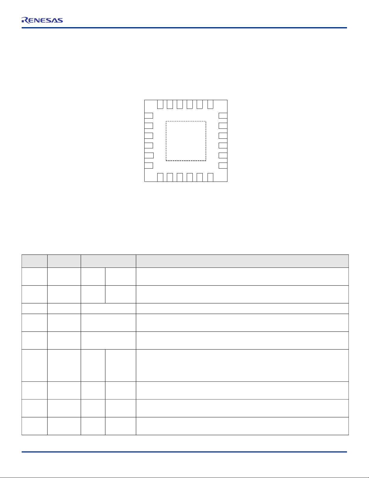
Pin Assignments
1
7
4 × 4 mm 24-VFQFPN
19
13
XOUT
XIN/REF
V
DDO
3
CLKIN
OUT3B
OUT2
CLKINB
CLKSEL
OUT3
OUT2B
V
DDO
2
V
DDA
SD/OE
SEL1/SDA
SEL0/SCL
V
DDO
4
OUT4
OUT4B
OUT1B
OUT1
V
DDO
1
V
DDD
V
DDO
0
OUT0_SEL_I2CB
EPAD
2
3
4
5
6
8
9101112
14
15
16
17
18
2021222324
Figure 1. Pin Assignments for 4 x 4 mm 24-VFQFPN Package – Top View
5P49V6965 Datasheet
Pin Descriptions
Table 1. Pin Descriptions
Number Name Type Description
Pull-down
Pull-down
Power
Pull-down
Pull-down
Pull-down
Pull-down
Internal
Internal
Internal
Internal
Internal
Internal
Differential clock input. Weak 100kΩ internal pull-down.
Complementary differential clock input. Weak 100kΩ internal pull-down.
Crystal oscillator interface input, or single-ended LVCMOS clock input. Input voltage needs
to be below 1.2V. Refer to the section Driving XIN/REF with a CMOS Driver.
Analog functions power supply pin. Connect to 1.8V to 3.3V. V
the same voltage applied.
Input clock select. Selects the active input reference source in manual switchover mode.
0 = XIN/REF, XOUT (default).
1 = CLKIN, CLKINB.
See Table 20. Input Clock Select for more details.
Enables/disables the outputs (OE) or powers down the chip (SD).
Configuration select pin, or I
2
C SDA input as selected by OUT0_SEL_I2CB. Weak internal
pull-down resistor.
2
Configuration select pin, or I
C SCL input as selected by OUT0_SEL_I2CB. Weak internal
pull-down resistor.
1 CLKIN Input
2 CLKINB Input
3 XOUT Output Crystal oscillator interface output.
4 XIN/REF Input
5 V
DDA
6 CLKSEL Input
7 SD/OE Input
8 SEL1/SDA Input
9 SEL0/SCL Input
DDA
and V
should have
DDD
3©2020 Renesas Electronics Corporation August 20, 2020
Page 4
Table 1. Pin Descriptions (Cont.)
Number Name Type Description
5P49V6965 Datasheet
10 V
4 Power Output power supply. Connect to 1.8 to 3.3V. Sets output voltage levels for OUT4/OUT4B.
DDO
11 OUT4 Output Output clock 4. Refer to the Output Drivers section for more details.
12 OUT4B Output Complementary output clock 4. Refer to the Output Drivers section for more details.
13 OUT3B Output Complementary output clock 3. Refer to the Output Drivers section for more details.
14 OUT3 Output Output clock 3. Refer to the Output Drivers section for more details.
15 V
3 Power Output power supply. Connect to 1.8 to 3.3V. Sets output voltage levels for OUT3/OUT3B.
DDO
16 OUT2B Output Complementary output clock 2. Refer to the Output Drivers section for more details.
17 OUT2 Output Output clock 2. Refer to the Output Drivers section for more details.
18 V
2 Power Output power supply. Connect to 1.8 to 3.3V. Sets output voltage levels for OUT2/OUT2B.
DDO
19 OUT1B Output Complementary output clock 1. Refer to the Output Drivers section for more details.
20 OUT1 Output Output clock 1. Refer to the Output Drivers section for more details.
21 V
22 V
23 V
1 Power Output power supply. Connect to 1.8 to 3.3V. Sets output voltage levels for OUT1/OUT1B.
DDO
DDD
0 Power
DDO
Power
Digital functions power supply pin. Connect to 1.8 to 3.3V. V
same voltage applied.
Power supply pin for OUT0_SEL_I2CB. Connect to 1.8 to 3.3V. Sets output voltage levels
for OUT0.
DDA
and V
should have the
DDD
Latched input/LVCMOS output. At power-up, the voltage at the pin OUT0_SEL_I2CB is
latched by the part and used to select the state of pins 8 and 9. If a weak pull-up (10kΩ) is
24
OUT0_SEL
_I2CB
Input/
Output
Internal
Pull-down
placed on OUT0_SEL_I2CB, pins 8 and 9 will be configured as hardware select pins, SEL1
and SEL0. If a weak pull-down (10kΩ) is placed on OUT0_SEL_I2CB or it is left floating,
pins 8 and 9 will act as the SDA and SCL pins of an I
2
C interface. After power-up, the pin
acts as an LVCMOS reference output.
25 GND GND Connect to ground pad.
4©2020 Renesas Electronics Corporation August 20, 2020
Page 5
5P49V6965 Datasheet
Absolute Maximum Ratings
The absolute maximum ratings are stress ratings only. Stresses greater than those listed below can cause permanent damage to the
device. Functional operation of the device at absolute maximum ratings is not implied. Exposure to absolute maximum rating conditions
may affect device reliability.
Table 2. Absolute Maximum Ratings
Item Rating
Supply Voltage, V
DDA
, V
DDD
, V
DDO
3.6V.
XIN/REF Input 1.2V.
CLKIN, CLKINB Input V
, 1.2V voltage swing.
DDO0
I2C Loading Current 10mA.
Storage Temperature, T
STG
-65°C to 150°C.
Junction Temperature 125°C
ESD Human Body Model 2000V.
Thermal Characteristics
Table 3. Thermal Characteristics
Symbol Parameter Value Units
θ
JA
θ
JB
θ
JC
Theta JA. Junction to air thermal impedance (0mps). 42 °C/W
Theta JB. Junction to board thermal impedance (0mps). 2.35 °C/W
Theta JC. Junction to case thermal impedance (0mps). 41.8 °C/W
Recommended Operating Conditions
Table 4. Recommended Operating Conditions
Symbol Parameter Minimum Typical Maximum Units
Power supply voltage for supporting 1.8V outputs. 1.71 1.8 1.89 V
V
V
V
DDOX
DDD
DDA
T
PU
T
A
C
L
Power supply voltage for supporting 2.5V outputs. 2.375 2.5 2.625 V
Power supply voltage for supporting 3.3V outputs. 3.135 3.3 3.465 V
Power supply voltage for core logic functions. 1.71 3.465 V
Analog power supply voltage. Use filtered analog power supply. 1.71 3.465 V
Power ramp time for all VDDs to reach 90% of VDD. 0.05 50 ms
Operating temperature, ambient. -40 85 °C
Maximum load capacitance (3.3V LVCMOS only). 15 pF
5©2020 Renesas Electronics Corporation August 20, 2020
Page 6
5P49V6965 Datasheet
Electrical Characteristics
Table 5. Current Consumption
V
, V
DDD
, V
DDA
Symbol Parameter Conditions Minimum Typical Maximum Units
I
DDCORE
I
DDOx
I
DDPD
= 3.3V ±5%, 2.5V ±5%, 1.8V ±5%, TA = -40°C to +85°C.
DDO0
1
Core Supply Current 100MHz on all outputs, 25MHz REFCLK. 33 42 mA
Output Buffer Supply
Current
LVPECL, 350MHz, 3.3V V
LVPECL, 350MHz, 2.5V V
LVDS, 350MHz, 3.3V V
LVDS, 350MHz, 2.5V V
LVDS, 350MHz, 1.8V V
HCSL, 250MHz, 3.3V V
HCSL, 250MHz, 2.5V V
DDOx2.
DDOx2.
DDOx2.
DDOx 2.
DDOx 2.
LVCMOS, 50MHz, 3.3V, V
LVCMOS, 50MHz, 2.5V, V
LVCMOS, 50MHz, 1.8V, V
LVCMOS, 200MHz, 3.3V V
LVCMOS, 200MHz, 2.5V V
LVCMOS, 200MHz, 1.8V V
DDOx.2.
DDOx.2.
DDOx
DDOx
DDOx
DDOx
DDOx
DDOx
2,3
. 22 27 mA
2,3
. 20 24 mA
2,3
. 17 21 mA
2,3
. 43 56 mA
2,3
. 33 43 mA
2,3
. 24 31 mA
45 58 mA
36 47 mA
26 32 mA
25 30 mA
22 27 mA
39 48 mA
37 46 mA
Power Down Current SD asserted, I2C programming. 10 12 mA
1
I
2
Measured into a 5” 50Ω trace. See Test Loads section for more details.
3
Single CMOS driver active.
DDCORE
= I
DDA
+ I
DDD
.
6©2020 Renesas Electronics Corporation August 20, 2020
Page 7
5P49V6965 Datasheet
Table 6. AC Timing Characteristics
V
, V
DDA
DDD
, V
= 3.3V ±5%, 2.5V ±5%, 1.8V ±5%, TA = -40°C to +85°C unless stated otherwise.
DDO0
Symbol Parameter Conditions Minimum Typical Maximum Units
Input frequency limit (crystal). 8 40 MHz
1
F
IN
Input Frequency
Input frequency limit (CLKIN,CLKINB). 1 350 MHz
Input frequency limit (single-ended over XIN). 1 200 MHz
F
OUT
f
T
VCO
DC
2
Output Frequency
Single-ended clock output limit (LVCMOS),
individual FOD mode.
Differential clock output limit
(LVPECL/LVDS/HCSL), individual FOD mode.
Single-ended clock output limit (LVCMOS),
cascaded FOD mode, output 2–4.
1 200
1 350
MHz
0.001 200
Differential clock output limit
(LVPECL/LVDS/HCSL), cascaded FOD mode,
0.001 350
output 2–4.
VCO Operating Frequency
Range
Measured at V
reference output, V
Measured at V
reference output, V
3
Output Duty Cycle
Measured at V
/2, all outputs except
DD
DD
DD
= 2.5V or 3.3V.
DDOX
/2, all outputs except
= 1.8V
DDOX
/2, reference output OUT0
(5MHz–150.1MHz) with 50% duty cycle input.
Measured at V
/2, reference output OUT0
DD
(150.1MHz–200MHz) with 50% duty cycle
2500 2900 MHz
45 50 55 %
40 50 60 %
40 50 60 %
30 50 70 %
input.
Skew between the same frequencies, with
T
SKEW
Output Skew
outputs using the same driver format and
phase delay set to 0ns.
Measured after all VDDs have risen above
T
STARTUP
4,5
Startup Time
90% of their target value 6.
PLL lock time from shutdown mode. 3 4 ms
1
Practical lower frequency is determined by loop filter settings.
2
A slew rate of 2.75V/ns or greater should be selected for output frequencies of 100MHz or higher.
3
Duty cycle is only guaranteed at maximum slew rate settings.
4
Actual PLL lock time depends on the loop configuration.
5
Includes loading the configuration bits from EPROM to PLL registers. It does not include EPROM programming/write time.
6
Power-up with temperature calibration enabled; contact Renesas if shorter lock-time is required in system.
7©2020 Renesas Electronics Corporation August 20, 2020
75 ps
30 ms
Page 8
5P49V6965 Datasheet
Table 7. General Input Characteristics
V
, V
DDA
DDD
, V
= 3.3V ±5%, 2.5V ±5%, 1.8V ±5%, TA = -40°C to +85°C unless stated otherwise.
DDO0
Symbol Parameter Conditions Minimum Typical Maximum Units
CLKIN,CLKINB,CLKSEL,SD/OE,SEL1/SD
A, SEL0/SCL.
CLKSEL, SD/OE, SEL1/SDA, SEL0/SCL,
CLKIN, CLKINB, OUT0_SEL_I2CB.
3 7 pF
100 300 kΩ
V
DDD
+ 0.3 V
DDD
DDD
+ 0.3 V
DDO0
T
C
R
V
V
V
V
V
V
R/TF
Input Capacitance
IN
Pull-down Resistor
PD
Input High Voltage CLKSEL, SD/OE. 0.7 x V
IH
Input Low Voltage CLKSEL, SD/OE. GND - 0.3 0.3 x V
IL
Input High Voltage OUT0_SEL_I2CB. 1.7 V
IH
Input Low Voltage OUT0_SEL_I2CB. GND - 0.3 0.4 V
IL
Input High Voltage XIN/REF. 0.8 1.2 V
IH
Input Low Voltage XIN/REF. GND - 0.3 0.4 V
IL
Input Rise/Fall Time CLKSEL, SD/OE, SEL1/SDA, SEL0/SCL. 300 ns
Table 8. CLKIN Electrical Characteristics
V
, V
DDA
DDD
, V
= 3.3V ±5%, 2.5V ±5%, 1.8V ±5%, TA = -40°C to +85°C unless stated otherwise.
DDO0
Symbol Parameter Conditions Minimum Typical Maximum Units
V
SWING
Input Amplitude – CLKIN, CLKINB Peak to peak value, single-ended. 200 1200 mV
dv/dt Input Slew Rate – CLKIN, CLKINB Measured differentially. 0.4 8 V/ns
V
DC
I
IL
I
IH
IN
Input Leakage Low Current VIN = GND. -5 5 μA
Input Leakage High Current VIN = 1.7V. 20 μA
Input Duty Cycle
Measurement from differential
waveform.
45 55 %
8©2020 Renesas Electronics Corporation August 20, 2020
Page 9
5P49V6965 Datasheet
Table 9. Electrical Characteristics – CMOS Outputs
V
, V
DDA
DDD
, V
= 3.3V ±5%, 2.5V ±5%, 1.8V ±5%, TA = -40°C to +85°C unless stated otherwise.
DDO0
Symbol Parameter Conditions Minimum Typical Maximum Units
V
OH
V
OL
R
OUT
T
SR
I
OZDD
Output High Voltage
IOH = -15mA (3.3V), -12mA (2.5V). 0.7 x V
= -8mA (1.8V). 0.5 x V
I
OH
DDO
DDO
V
V
DDO
DDO
Output Low Voltage IOL = 15mA (3.3V), 12mA (2.5V), 8mA (1.8V). 0.45 V
Output Driver Impedance CMOS output driver. 17 Ω
Slew Rate, SLEW[1:0] = 00
Slew Rate, SLEW[1:0] = 01 1.2 2.3
Slew Rate, SLEW[1:0] = 10 1.3 2.4
Single-ended 3.3V LVCMOS output clock rise and
fall time, 20% to 80% of V
= 3.3V.
V
DDOX
(output load = 5pF)
DDO
1.0 2.2
Slew Rate, SLEW[1:0] = 11 1.7 2.7
Slew Rate, SLEW[1:0] = 00
Slew Rate, SLEW[1:0] = 01 0.7 1.4
Slew Rate, SLEW[1:0] = 10 0.6 1.4
Single-ended 2.5V LVCMOS output clock rise and
fall time, 20% to 80% of V
= 2.5V.
V
DDOX
(output load = 5pF)
DDO
0.6 1.3
V/ns
Slew Rate, SLEW[1:0] = 11 1.0 1.7
Slew Rate, SLEW[1:0] = 00
Slew Rate, SLEW[1:0] = 01 0.4 0.8
Slew Rate, SLEW[1:0] = 10 0.4 0.9
Single-ended 1.8V LVCMOS output clock rise and
fall time, 20% to 80% of V
= 1.8V.
V
DD
(output load = 5pF)
DDO
0.3 0.7
Slew Rate, SLEW[1:0] = 11 0.7 1.2
Output Leakage Current
(OUT1–4)
Tri-state outputs. 5 μA
Output Leakage Current (OUT0) Tri-state outputs. 30 μA
V
V
Table 10. Electrical Characteristics – LVDS Outputs
V
, V
DDA
DDD
, V
= 3.3V ±5%, 2.5V ±5%, 1.8V ±5%, TA = -40°C to +85°C unless stated otherwise.
DDO0
Symbol Parameter Minimum Typical Maximum Units
(+) Differential Output Voltage for the TRUE Binary State 247 454 mV
V
OT
(-) Differential Output Voltage for the FALSE Binary State -454 -247 mV
V
OT
Change in VOT between Complimentary Output States 50 mV
ΔV
OT
Output Common Mode Voltage (Offset Voltage) at 3.3 V ±5%, 2.5V ±5% 1.125 1.25 1.375 V
V
ΔV
I
OS
I
OS
OSD
T
R
T
OS
F
Output Common Mode Voltage (Offset Voltage) at 1.8V ±5% 0.8 0.875 0.96 V
Change in VOS between Complimentary Output States 50 mV
Outputs Short Circuit Current, V
Differential Outputs Short Circuit Current, V
OUT
+ or V
- = 0V or V
OUT
+ = V
OUT
DDO
- 6 12 mA
OUT
9 24 mA
LVDS rise time 20%–80% 300 ps
LVDS fall time 80%–20% 300 ps
9©2020 Renesas Electronics Corporation August 20, 2020
Page 10

5P49V6965 Datasheet
Table 11. Electrical Characteristics – LVPECL Outputs
V
, V
DDA
DDD
, V
= 3.3V ±5%, 2.5V ±5%, TA = -40°C to +85°C unless stated otherwise.
DDO0
Symbol Parameter Minimum Typical Maximum Units
V
V
V
SWING
T
T
Output Voltage High, Terminated through 50Ω tied to V
OH
Output Voltage Low, Terminated through 50Ω tied to V
OL
Peak-to-Peak Differential Output Voltage Swing 1.1 2 V
LVPECL rise time 20%–80% 400 ps
R
LVPECL fall time 80%–20% 400 ps
F
Table 12. Electrical Characteristics – HCSL Outputs
V
, V
DDA
DDD
, V
= 3.3V ±5%, 2.5V ±5%, TA = -40°C to +85°C unless stated otherwise.
DDO0
- 2V V
DD
- 2V V
DD
1
- 1.19 V
DDO
- 1.94 V
DDO
- 0.69 V
DDO
- 1.4 V
DDO
Symbol Parameter Conditions Minimum Typical Maximum Units
2,3
dV/dt Slew Rate Scope averaging on
ΔdV/dt Slew Rate Matching Scope averaging on
V
MAX
V
MIN
V
SWING
V
CROSS
ΔV
CROSS
1
Guaranteed by design and characterization. Not 100% tested in production.
2
Measured from differential waveform.
3
Slew rate is measured through the V
4
V
CROSS
Maximum Voltage
Minimum Voltage -300 mV
Measurement on single-ended signal using absolute
value (scope averaging off).
Voltage Swing Scope averaging off
Crossing Voltage Value Scope averaging off
Crossing Voltage Variation Scope averaging off 5. 140 mV
voltage range centered around differential 0V. This results in a ±150mV window around differential 0V.
SWING
is defined as voltage where Clock = Clock# measured on a component test board and only applies to the differential rising edge (i.e. Clock
. 1 4 V/ns
2,3
. 20 %
1150 mV
2,6
. 300 mV
4,6
. 250 550 mV
rising and Clock# falling).
5
The total variation of all V
The intent is to limit V
6
Measured from single-ended waveform.
CROSS
measurements in any particular system. Note that this is a subset of V
CROSS
induced modulation by setting ΔV
to be smaller than V
CROSS
CROSS
CROSS
absolute.
min/max (V
absolute) allowed.
CROSS
Table 13. Spread Spectrum Generation Specifications
Symbol Parameter Conditions Minimum Typical Maximum Units
f
SSOUT
f
MOD
Spread Frequency Output frequency range for spread spectrum. 5 300 MHz
Mod Frequency Modulation frequency. 30 to 63 kHz
Amount of spread value (programmable)–center spread. ±0.1% to ±2.5%
f
SPREAD
Spread Value
Amount of spread value (programmable)–down spread. -0.2% to -5%
10©2020 Renesas Electronics Corporation August 20, 2020
%f
OUT
Page 11

I2C Bus Characteristics
5P49V6965 Datasheet
Table 14. I
2
C Bus (SCL/SDA) DC Characteristics
Symbol Parameter Conditions Minimum Typical Maximum Units
For SEL1/SDA pin and
SEL0/SCL pin.
For SEL1/SDA pin and
SEL0/SCL pin.
0.7 x V
DDD
DDD
0.3 x V
DDD
V
V
V
V
IH
IL
HYS
I
IN
OL
Input High Level
Input Low Level
Hysteresis of Inputs 0.05 x V
Input Leakage Current -1 36 μA
Output Low Voltage IOL = 3mA. 0.45 V
Table 15. I2C Bus (SCL/SDA) AC Characteristics
Symbol Parameter Conditions Minimum Typical Maximum Units
F
SCLK
t
BUF
t
SU:START
t
HD:START
t
SU:DATA
t
HD:DATA
t
OVD
C
B
t
R
t
F
t
HIGH
t
LOW
t
SU:STOP
1
A device must internally provide a hold time of at least 300ns for the SDA signal (referred to the V
Serial Clock Frequency (SCL) — 10 400 kHz
Bus Free Time between Stop and Start — 1.3 μs
Setup Time, Start — 0.6 μs
Hold Time, Start — 0.6 μs
Setup Time, Data Input (SDA) — 0.1 μs
Hold Time, Data Input (SDA)
1
— 0 μs
Output Data Valid from Clock — 0.9 μs
Capacitive Load for Each Bus Line — 400 pF
Rise Time, Data and Clock (SDA, SCL) — 20 + 0.1 x C
Fall Time, Data and Clock (SDA, SCL) — 20 + 0.1 x C
B
B
300 ns
300 ns
High Time, Clock (SCL) — 0.6 μs
Low Time, Clock (SCL) — 1.3 μs
Setup Time, Stop — 0.6 μs
of the SCL signal) to bridge the undefined
IH(MIN)
region of the falling edge of SCL.
2 I2
C inputs are 3.3V tolerant.
V
V
V
11©2020 Renesas Electronics Corporation August 20, 2020
Page 12

Test Loads
33 Ohm
5pF
Zo = 50 Ohm
Test
Point
Device
2pF
Differential
Zo = 100 Ohm
33 Ohm
Device
33 Ohm
50 Ohm
2pF
50 Ohm
Test
Points
Differential
Zo = 100 Ohm
100 Ohm
Test
Points
Device
2pF
2pF
Differential
Zo = 100 Ohm
Test
Points
Device
50Ohm 50 Ohm
R
2pF2pF
R = 50 Ohm for 3.3V LVPECL
R = 18 Ohm for 2.5V LVPECL
Figure 2. LVCMOS Test Load
Figure 3. HCSL Test Load
5P49V6965 Datasheet
Figure 4. LVDS Test Load
Figure 5. LVPECL Test Load
12©2020 Renesas Electronics Corporation August 20, 2020
Page 13

Jitter Performance Characteristics
Figure 6. Typical Phase Jitter Plot at 156.25MHz
5P49V6965 Datasheet
Note: Measured with OUT2 = 156.25MHz on, 39.625MHz input.
Table 16. Jitter Performance
1,2
Symbol Parameter Conditions Minimum Typical Maximum Units
LVCMOS 3.3V ±5%, -40°C–90°C. 5 30 ps
J
CY-CY
Cycle to Cycle Jitter
All differential outputs 3.3V ±5%, -40°C–90°C. 25 35 ps
LVCMOS 3.3V ±5%, -40°C–90°C. 28 40 ps
J
PK-PK
Period Jitter
All differential outputs 3.3V ±5%, -40°C–90°C. 4 30 ps
LVCMOS 3.3V ±5%, -40°C–90°C. 0.3 ps
J
1
Measured with 25MHz crystal input.
2
Configured with OUT0 = 25MHz–LVCMOS; OUT1 = 100MHz–HCSL; OUT2 = 125MHz–LVDS; OUT3 = 156.25MHz–LVPECL.
RMS Phase Jitter (12kHz–20MHz)
RMS
All differential outputs 3.3V ±5%, -40°C–90°C. 0.5 ps
13©2020 Renesas Electronics Corporation August 20, 2020
Page 14

5P49V6965 Datasheet
PCI Express Jitter Performance and Specification
Table 17. PCI Express Jitter Performance (Spread Spectrum = Off)
Parameter Symbol Conditions Minimum Typical Maximum Limit Units Notes
PCIe Phase Jitter
(Common Clocked
Architectures)
PCIe Phase Jitter
(SRNS Architectures)
t
jphPCIeG1-CC
t
jphPCIeG2-CC
t
jphPCIeG3-CC
t
jphPCIeG4-CC
t
jphPCIeG5-CC
t
jphPCIeG1-SRNS
t
jphPCIeG2-SRNS
t
jphPCIeG3-SRNS
t
jphPCIeG4-SRNS
PCIe Gen1 (2.5 GT/s)
SSC = OFF
PCIe Gen2 Lo Band (5.0 GT/s)
SSC = OFF
PCIe Gen2 Hi Band (5.0 GT/s)
SSC = OFF
PCIe Gen3 (8.0 GT/s)
SSC = OFF
PCIe Gen4 (16.0 GT/s)
SSC = OFF
PCIe Gen5 (32.0 GT/s)
SSC = OFF
PCIe Gen1 (2.5 GT/s)
SSC = OFF
PCIe Gen2 (5.0 GT/s)
SSC = OFF
PCIe Gen3 (8.0 GT/s)
SSC = OFF
PCIe Gen4 (16.0 GT/s)
SSC = OFF
4 86
0.05 3
0.22 3.1
0.12 1
0.12 0.5
0.05 0.15
0.3
0.26
0.07
N/A
0.07
ps
(p-p)
ps
(RMS)
ps
(RMS)
ps
(RMS)
ps
(RMS)
ps
(RMS)
ps
(p-p)
ps
(RMS)
ps
(RMS)
ps
(RMS)
1,2
1,2
1,2
1,2
1,2,3,4
1,2,3,5
1,2,6
1,2,6
1,2,6
1,2,6
t
jphPCIeG5-SRNS
1
The Refclk jitter is measured after applying the filter functions found in PCI Express Base Specification 5.0, Revision 1.0. See the Test Loads section
of the data sheet for the exact measurement setup. The worst case results for each data rate are summarized in this table.
2
Jitter measurements shall be made with a capture of at least 100,000 clock cycles captured by a real-time oscilloscope (RTO) with a sample rate
of 20GS/s or greater. Broadband oscilloscope noise must be minimized in the measurement. The measured PP jitter is used (no extrapolation) for
RTO measurements. Alternately, jitter measurements may be used with a Phase Noise Analyzer (PNA) extending (flat) and integrating and folding
the frequency content up to an offset from the carrier frequency of at least 200MHz (at 300MHz absolute frequency) below the Nyquist frequency.
For PNA measurements for the 2.5GT/s data rate, the RMS jitter is converted to peak to peak jitter using a multiplication factor of 8.83. In the case
where real-time oscilloscope and PNA measurements have both been done and produce different results, the RTO result must be used.
3
SSC spurs from the fundamental and harmonics are removed up to a cutoff frequency of 2MHz taking care to minimize removal of any non-SSC
content.
4
Note that 0.7ps RMS is to be used in channel simulations to account for additional noise in a real system.
5
Note that 0.25ps RMS is to be used in channel simulations to account for additional noise in a real system.
6
While the PCI Express Base Specification 5.0, Revision 1.0 provides the filters necessary to calculate SRIS jitter values, it does not provide
specification limits, hence the n/a in the Limit column. SRIS values are informative only. In general, a clock operating in an SRIS system must be
twice as good as a clock operating in a Common Clock system. For RMS values, twice as good is equivalent to dividing the CC value by Ö2.
PCIe Gen5 (32.0 GT/s)
SSC = OFF
0.07
ps
(RMS)
1,2,6
14©2020 Renesas Electronics Corporation August 20, 2020
Page 15

5P49V6965 Datasheet
Table 18. PCI Express Jitter Performance (Spread Spectrum = On)
Parameter Symbol Conditions Minimum Typical Maximum Limit Units Notes
PCIe Phase Jitter
(Common Clocked
Architectures)
PCIe Phase Jitter
(SRIS Architectures)
t
jphPCIeG1-CC
t
jphPCIeG2-CC
t
jphPCIeG3-CC
t
jphPCIeG4-CC
t
jphPCIeG5-CC
t
jphPCIeG1-SRIS
t
jphPCIeG2-SRIS
t
jphPCIeG3-SRIS
t
jphPCIeG4-SRIS
PCIe Gen 1 (2.5 GT/s)
-0.5%
SSC ≤
PCIe Gen 2 Lo Band (5.0 GT/s)
SSC ≤ -0.5%
PCIe Gen 2 Hi Band (5.0 GT/s)
SSC ≤ -0.5%
PCIe Gen 3 (8.0 GT/s)
SSC ≤ -0.5%
PCIe Gen 4 (16.0 GT/s)
SSC ≤ -0.5%
PCIe Gen 5 (32.0 GT/s)
SSC ≤ -0.5%
PCIe Gen 1 (2.5 GT/s)
SSC ≤ -0.3%
PCIe Gen 2 (5.0 GT/s)
SSC ≤ -0.3%
PCIe Gen 3 (8.0 GT/s)
SSC ≤ -0.3%
PCIe Gen 4 (16.0 GT/s)
SSC ≤ -0.3%
16 86
0.02 3
0.92 3.1
0.37 1
0.37 0.5
N/A 0.15
14
1.4
0.42
N/A
0.36
ps
(p-p)
ps
(RMS)
ps
(RMS)
ps
(RMS)
ps
(RMS)
ps
(RMS)
ps
(p-p)
ps
(RMS)
ps
(RMS)
ps
(RMS)
1,2
1,2
1,2
1,2
1,2,3,4
1,2,3,5
1,2,6
1,2,6
1,2,6
1,2,6
t
jphPCIeG5-SRIS
1
The Refclk jitter is measured after applying the filter functions found in PCI Express Base Specification 5.0, Revision 1.0. See the Test Loads section
of the data sheet for the exact measurement setup. The worst case results for each data rate are summarized in this table.
2
Jitter measurements shall be made with a capture of at least 100,000 clock cycles captured by a real-time oscilloscope (RTO) with a sample rate
of 20GS/s or greater. Broadband oscilloscope noise must be minimized in the measurement. The measured PP jitter is used (no extrapolation) for
RTO measurements. Alternately, jitter measurements may be used with a Phase Noise Analyzer (PNA) extending (flat) and integrating and folding
the frequency content up to an offset from the carrier frequency of at least 200MHz (at 300MHz absolute frequency) below the Nyquist frequency.
For PNA measurements for the 2.5GT/s data rate, the RMS jitter is converted to peak to peak jitter using a multiplication factor of 8.83. In the case
where real-time oscilloscope and PNA measurements have both been done and produce different results, the RTO result must be used.
3
SSC spurs from the fundamental and harmonics are removed up to a cutoff frequency of 2MHz taking care to minimize removal of any non-SSC
content.
4
Note that 0.7ps RMS is to be used in channel simulations to account for additional noise in a real system.
5
Note that 0.25ps RMS is to be used in channel simulations to account for additional noise in a real system.
6
While the PCI Express Base Specification 5.0, Revision 1.0 provides the filters necessary to calculate SRIS jitter values, it does not provide
specification limits, hence the n/a in the Limit column. SRIS values are informative only. In general, a clock operating in an SRIS system must be
twice as good as a clock operating in a Common Clock system. For RMS values, twice as good is equivalent to dividing the CC value by Ö2.
PCIe Gen 5 (32.0 GT/s)
SSC ≤ -0.3%
N/A
ps
(RMS)
1,2,6
15©2020 Renesas Electronics Corporation August 20, 2020
Page 16

Features and Functional Blocks
XIN/REF
XOUT
CLKIN
CLKINB
CLKSEL
OTP
and
Control
Logic
PRIMSRC
Reg 0x13[1]
5P49V6965 Datasheet
Device Startup and Power-On-Reset
The device has an internal power-up reset (POR) circuit. All VDDs
must be connected to desired supply voltage to trigger POR.
User can define specific default configurations through internal
One-Time-Programmable (OTP) memory. Either customer or
factory can program the default configuration. Please refer to
VersaClock 6E Family Register Descriptions and Programming
Guide for details or contact Renesas if a specific
factory-programmed default configuration is required.
Device will identity which of the 2 modes to operate in by the state
of OUT0_SEL_I2CB pin at POR. Both of the 2 modes default
configurations can be programmed as stated above.
1. Software Mode (I
2
C interface will be open to users for in-system programming,
I
overriding device default configurations at any time.
2. Hardware Select Mode: OUT0_SEL_I2CB is high at POR.
Device has been programmed to load OTP at power-up
(REG0[7]=1). The device will load internal registers according
to Table 19. Power-up Behavior.
Internal OTP memory can support up to 4 configurations,
selectable by SEL0/SEL1 pins.
At POR, logic levels at SEL0 and SEL1 pins must be settled,
resulting the selected configuration to be loaded at power up.
After the first 10ms of operation, the levels of the SELx pins
can be changed, either to low or to the same level as
V
DDD/VDDA
of < 300ns rise/fall time and only a single pin can be changed
at a time. After a pin level change, the device must not be
interrupted for at least 1ms so that the new values have time to
load and take effect.
2
C): OUT0_SEL_I2CB is low at POR.
. The SELx pins must be driven with a digital signal
Reference Clock and Selection
The device supports up to two clock inputs.
▪ Crystal input, can be driven by a single-ended clock.
▪ Clock input (CLKIN, CLKINB), a fully differential input that only
accepts a reference clock. A single-ended clock can also drive
it on CLKIN.
Figure 7. Clock Input Diagram, Internal Logic
Manual Switchover
The CLKSEL pin selects the input clock between either XTAL/REF
or (CLKIN, CLKINB).
CLKSEL polarity can be changed by I
0x13[1]) as shown in the table below.
0 = XIN/REF, XOUT (default); 1 = CLKIN, CLKINB.
Table 20. Input Clock Select
PRIMSRC CLKSEL Source
2
C programming (Byte
Table 19. Power-up Behavior
OUT0_SEL_I2CB
at POR SEL1 SEL0
1 0 0 No 0 0
1 0 1 No 0 1
1 1 0 No 0 2
1 1 1 No 0 3
0 X X Yes 1
0 X X Yes 0 0
I2C
Access REG0:7 Config
2
C
I
defaults
0 0 XIN/REF
0 1 CLKIN, CLKINB
1 0 CLKIN, CLKINB
1 1 XIN/REF
When SM[1:0] is “0x”, the redundant inputs are in manual
switchover mode. In this mode, CLKSEL pin is used to switch
between the primary and secondary clock sources. The PRIMSRC
bit determines the primary and secondary clock source setting.
During the switchover, no glitches will occur at the output of the
device, although there may be frequency and phase drift,
depending on the exact phase and frequency relationship
between the primary and secondary clocks.
16©2020 Renesas Electronics Corporation August 20, 2020
Page 17

5P49V6965 Datasheet
Internal Crystal Oscillator (XIN/REF)
Choosing Crystals
A crystal manufacturer will calibrate its crystals to the nominal
frequency with a certain load capacitance value. When the
oscillator load capacitance matches the crystal load capacitance,
the oscillation frequency will be accurate. When the oscillator load
capacitance is lower than the crystal load capacitance, the
oscillation frequency will be higher than nominal and vice versa so
for an accurate oscillation frequency you need to make sure to
match the oscillator load capacitance with the crystal load
capacitance.
Tuning the Crystal Load Capacitor
Ci1 and Ci2 are commonly programmed to be the same value.
Adjustment of the crystal tuning capacitors allows maximum
flexibility to accommodate crystals from various manufacturers.
The range of tuning capacitor values available are in accordance
with the following table.
Ci1/Ci2 starts at 9pF with setting 000000b and can be increased
up to 25pF with setting 111111b. The step per bit is 0.5pF.
Table 21. XTAL[5:0] Tuning Capacitor
Parameter Bits Step (pF) Minimum (pF) Maximum (pF)
XTAL 6 0.5 9 25
You can write the following equation for this capacitance:
Ci = 9pF + 0.5pF × XTAL[5:0]
C
= Ci1 + Cs1 + Ce1
XIN
C
= Ci2 + Cs2 + Ce2
XOUT
The final load capacitance of the crystal:
C
= C
XIN
× C
L
XOUT
/ (C
XIN
+ C
XOUT
)
It is recommended to set the same value for capacitors the same
at each crystal pin, meaning:
C
= C
XIN
XOUT
Example 1: The crystal load capacitance is specified as 8pF and
the stray capacitance at each crystal pin is Cs = 1.5pF. Assuming
equal capacitance value at XIN and XOUT, the equation is as
Cs1 and Cs2 are stray capacitances at each crystal pin and
follows:
typical values are between 1pF and 3pF.
8pF = (9pF + 0.5pF × XTAL[5:0] + 1.5pF) / 2
Ce1 and Ce2 are additional external capacitors, increasing the
So, XTAL[5:0] = 11 (decimal).
load capacitance reduces the oscillator gain so please consult the
factory when adding Ce1 and/or Ce2 to avoid crystal startup
issues. Ci1 and Ci2 are integrated programmable load capacitors,
one at XIN and one at XOUT. Ci1 and Ci2.
Example 2: The crystal load capacitance is specified as 12pF and
the stray capacitance Cs is unknown. Footprints for external
capacitors Ce are added and a worst case Cs of 5pF is used. For
now we use Cs + Ce = 5pF and the right value for Ce can be
The value of each capacitor is composed of a fixed capacitance
determined later to make 5pF together with Cs.
amount plus a variable capacitance amount set with the XTAL[5:0]
register.
12pF = (9pF + 0.5pF × XTAL[5:0] + 5pF) / 2
So, XTAL[5:0] = 20 (decimal).
Table 22. Recommended Crystal Characteristics
Parameter Minimum Typical Maximum Units
Mode of Oscillation Fundamental
Frequency 8 25 40 MHz
Equivalent Series Resistance (ESR) 10 100 Ω
Shunt Capacitance 7 pF
Load Capacitance (C
Load Capacitance (C
Maximum Crystal Drive Level 100 μW
) at < = 25MHz 6 8 12 pF
L
) > 25MHz to 40MHz 6 8 pF
L
17©2020 Renesas Electronics Corporation August 20, 2020
Page 18

5P49V6965 Datasheet
Programmable Loop Filter
The device PLL loop bandwidth range depends on the input
reference frequency (Fref).
Table 23. Loop Filter Settings
Input Reference
Frequency (MHz)
1 40 126
350 300 1000
Loop Bandwidth
Minimum (kHz)
Loop Bandwidth
Maximum (kHz)
Fractional Output Dividers (FOD)
The device has 4 fractional output dividers (FOD). Each of the
FODs are comprised of a 12-bit integer counter, and a 24-bit
fractional counter. The output divider can operate in integer divide
only mode for improved performance, or utilize the fractional
counters to generate a clock frequency accurate to 50ppb.
FOD has the following features:
Individual Spread Spectrum Modulation
The output clock frequencies can be modulated to spread energy
across a broader range of frequencies, lowering system EMI.
When device is at hardware select mode outputs will be
automatically aligned at POR. The same synchronization reset is
also triggered when switching between configurations with the
SEL0/1 pins. This ensures that the outputs remain aligned in
every configuration.
When using software mode I
during operation, alignment can be lost. Alignment can be
restored by manually triggering the reset through I
The outputs are aligned on the falling edges of each output by
default. Rising edge alignment can also be achieved by utilizing
the programmable skew feature to delay the faster clock by 180
degrees. The programmable skew feature also allows for fine
tuning of the alignment.
Programmable Skew
The device has the ability to skew outputs by quadrature values.
The skew on each output can be adjusted from 0 to 360 degrees.
Skew is adjusted in units equal to 1/32 of the VCO period. So, for
100MHz output and a 2800MHz VCO, you can select how many
11.161ps units you want added to your skew (resulting in units of
0.402 degrees). For example, 0, 0.402, 0.804, 1.206, 1.408, and
so on. The granularity of the skew adjustment is always
dependent on the VCO period and the output period.
2
C to reprogram an output divider
2
C.
Each divider has individual spread ability. Spread modulation
independent of output frequency, a triangle wave modulation
between 30 and 63kHz.
Spread spectrum can be applied to any output clock, any clock
frequency, and any spread amount from ±0.25% to ±2.5%
center-spread and -0.5% to -5% down-spread.
Bypass Mode
Bypass mode (divide by 1) to allow the output to behave as a
buffered copy from the input or another FOD.
Cascaded Mode
As shown in the block diagram, FODs can be cascaded for lower
output frequency.
For example, user currently has OUT1 running at 12.288MHz and
needs another 48kHz output. The user can cascade FOD2 by
taking input from OUT1, with a divide ratio of 256. In this way,
OUT 2 is running at 48kHz while in alignment with 12.288MHz on
OUT1.
Dividers Alignment
Each output divider block has a synchronizing pulse to provide
startup alignment between outputs dividers. This allows alignment
of outputs for low skew performance.
Output Drivers
The device output drivers support the following features
individually:
▪ 2.5V or 3.3V voltage level for HCSL/LVPECL operation
▪ 1.8V, 2.5V or 3.3V voltage levels for CMOS/LVDS operation
▪ CMOS supports 4 operating modes:
• CMOSD: OUTx and OUTxB 180 degrees out of phase
• CMOSX2: OUTx and OUTxB phase-aligned
• CMOS1: only OUTx pin is on
• CMOS2: only OUTxB pin is on
When a given output is configured to at CMOSD or CMOSX2, then
all previously described configuration and control apply equally to
both pins.
▪ Independent output enable/disabled by register bits. When
disabled, an output can be either in a logic 1 state or Hi-Z.
The following options are used to disable outputs:
1. Output turned off by I
2. Output turned off by SD/OE pin.
3. Output unused, which means is turned off regardless of OE pin
status.
2
C.
18©2020 Renesas Electronics Corporation August 20, 2020
Page 19

5P49V6965 Datasheet
SD/OE Pin Function
SD/OE pin can be programmed as following functions:
1. OE output enable (low active).
2. OE output enable (high active).
3. Global shutdown (low active).
4. Global shutdown (high active).
Output behavior when disabled is also programmable. User will
have the option to choose output driver behavior when it's off:
1. OUTx pin high, OUTxB pin low. (Controlled by SD/OE pin).
2. OUTx/OUTxB Hi-Z (Controlled by SD/OE pin).
3. OUTx pin high, OUTxB pin low. (Configured through I
4. OUTx/OUTxB Hi-Z (Configured by I
2
C).
The user has the option to disable the output with either I
SD/OE pin. Refer to VersaClock 6E Family Register Descriptions
and Programming Guide for details.
Figure 8. I2C R/W Sequence
2
C).
2
C or
I2C Operation
The device acts as a slave device on the I2C bus using one of the
2
two I
C addresses (0xD0 or 0xD4) to allow multiple devices to be
used in the system. The interface accepts byte-oriented block
write and block read operations.
Address bytes(2 bytes) specify the register address of the byte
position of the first register to write or read.
Data bytes (registers) are accessed in sequential order from the
lowest to the highest byte (most significant bit first).
Read and write block transfers can be stopped after any complete
byte transfer. During a write operation, data will not be moved into
the registers until the STOP bit is received, at which point, all data
received in the block write will be written simultaneously.
For full electrical I
SDATA and SCLK.
2
C compliance, use external pull-up resistors for
19©2020 Renesas Electronics Corporation August 20, 2020
Page 20

Typical Application Circuits
8
8
7
7
6
6
5
5
4
4
3
3
2
2
1
1
D D
C C
B B
A A
Layout notes:
1. Separate Xout and Xin Traces by 3 x the trace width
2. Do not share crystal load capacitor ground via with
other components.
3. Route power from bead through bulk capacitor pad
then through 0.1uF capacitor pad then to clock chip
Vdd pad.
4. Do not share ground vias. One ground pin one ground
via.
Revision history
0.1 11/30/16 first publication
Manufacture Part Number Z@100MHz PkgSz DC res. Current(Ma)
Fair-Rite 2504021217Y0 120 0402 0.5 200
muRata BLM15AG221SN1 220 0402 0.35 300
muRata BLM15BB121SN1 120 0402 0.35 300
TDK MMZ1005S241A 240 0402 0.18 200
TECSTAR TB4532153121 120 0402 0.3 300
NOTE:FERRITE BEAD FB1 =
PLACE NEAR
I2C CONTROLLER
IF USED
LVDS TERMINATION
3.3V LVPECL TERMINATION
2.5V and 3.3V HCSL TERMINATION
CONFIGURATION
PULL-UP FOR
HARDWARE
CONTROL
REMOVE FOR I2C
LVCMOS TERMINATION
FOR LVDS, LVPECL USE
TERMINATION ON RIGHT BEFORE
AC COUPLING
following pins have
weak internal
pull down resistors:
6, 7, 8, 9 and 24
for pins#: 22,23,21,18,15,10
pin# 5
FG_X1
OUT_0_SEL-I2C
V1P8VC
V1P8VC
OUTR0
CLKIN
CLKINB V1P8VC
OUTR1
CLKSEL OUTRB1
SDA V1P8VC
SCL OUTR2
OUTRB2
SD/OE
SDA
SCL CLKIN
CLKINB
OUT_0_SEL-I2C
FG_X2
V1P8VC V1P8VCA
V1P8VCA
OUTR3
OUTRB3
V1P8VC
OUTR4
OUTRB4
V1P8VC
VCC1P8
V3P3
V1P8VC
Size
Document Number Re v
Date: Sheet
of
0.1
Integrated Device Technology
A
11Wednesday, November 30, 2016
5P49V6965_SCH
San Jose, CA
Size
Document Number Re v
Date: Sheet
of
0.1
Integrated Device Technology
A
11Wednesday, November 30, 2016
5P49V6965_SCH
San Jose, CA
Size
Document Number Re v
Date: Sheet
of
0.1
Integrated Device Technology
A
11Wednesday, November 30, 2016
5P49V6965_SCH
San Jose, CA
R3 100
1 2
R2
2.2
1 2
C14
.1uF
12
C11
.1uF
12
FB1
SIGNAL_BEAD
1 2
U2
RECEIVER
1
2
R12 50
1 2
R9
10K
1 2
C5
.1uF
12
C8
.1uF
12
R5
49.9
1%
1 2
U4
RECEIVER
1
2
R14 33
1 2
C4
.1uF
12
C13 .1uF
1 2
R11 50
1 2
R10 50
1 2
R8
10K
1 2
C15
.1uF
12
R6 33
1 2
R4
49.9
1%
1 2
C3
.1uF
12
R15 33
1 2
C1
10uF
12
C7
NP
12
U5
5P49V6965A
XOUT3XIN/REF4CLKIN1CLKINB2CLKSEL6SEL1/SDA
8
SEL0/SCL9SD/OE
7
VDDA
5
VDDD
22
VDDO0
23
OUT0_SEL_I2CB
24
VDDO1
21
OUT1
20
OUT1B
19
VDDO2
18
OUT2
17
OUT2B
16
VDDO3
15
OUT3
14
OUT3B
13
VDDO4
10
OUT4
11
OUT4B
12
EPAD
25
EPAD
26
EPAD
27
EPAD
28
EPAD
29
EPAD
30
EPAD
31
EPAD
32
EPAD
33
R13 33
1 2
GNDGND
Y1
25.000 MHz
CL = 8pF
4
1
2
3
U3
RECEIVER
1
2
C12 .1uF
1 2
C6
NP
12
R7
10K
1 2
C2
1uF
12
Figure 9. Application Circuit Example
5P49V6965 Datasheet
20©2020 Renesas Electronics Corporation August 20, 2020
Page 21

5P49V6965 Datasheet
XO U T
XIN / REF
1 nF
Zo = 50 Ohm
Ro + Rs = 50 ohm
LVCMOS
VDD
Rs
Ro
R1
C3
R2
V_XIN
XOU T
XIN / REF
1 nF
5050
50
Zo = 50 Ohm
+3.3V LVPECL Driver
Zo = 50 Ohm
R2
R1
R3
C1
Input – Driving the XIN/REF or CLKIN
Driving XIN/REF with a CMOS Driver
In some cases, it is encouraged to have XIN/REF driven by a clock input for reasons like better SNR, multiple input select with device
CLKIN, etc. The XIN/REF pin is able to take an input when its amplitude is between 500mV and 1.2V and the slew rate more than
0.2V/ns.
The XIN/REF input can be overdriven by an LVCMOS driver or by one side of a differential driver through an AC coupling capacitor. The
XOUT pin can be left floating.
Figure 10. Overdriving XIN with a CMOS Driver
Table 24. Nominal Voltage Divider Values for Overdriving XIN with Single-ended Driver
LVCMOS Diver V
DD
Ro + Rs R1 R2 V_XIN (peak) Ro+Rs+R1+R2
3.3 50.0 130 75 0.97 255
2.5 50.0 100 100 1.00 250
1.8 50.0 62 130 0.97 242
Driving XIN with an LVPECL Driver
Figure 11 shows an example of the interface diagram for a +3.3V LVPECL driver. This is a standard LVPECL termination with one side of
the driver feeding the XIN/REF input. It is recommended that all components in the schematics be placed in the layout; though some
components might not be used, they can be utilized for debugging purposes. The datasheet specifications are characterized and
guaranteed by using a quartz crystal as the input. If the driver is 2.5V LVPECL, the only change necessary is to use the appropriate value
of R3.
Figure 11. Overdriving XIN with an LVPECL Driver
21©2020 Renesas Electronics Corporation August 20, 2020
Page 22

5P49V6965 Datasheet
R1
R2
Vrx
V er s aCloc k 5 Rec eive r
CLKI N
CLKI NB
LV CMOS
VDD
Zo = 50 Ohm
Ro + Rs = 5 0
Rs
Ro
Zo=50ohm
Zo=50ohm
CLKIN
CLKINB
VersaClock 6 Receiver
Q
nQ
Wiring the CLKIN Pin to Accept Single-ended Inputs
CLKIN cannot take a signal larger than 1.2V pk-pk due to the 1.2V regulated input inside. However, it is internally AC coupled so it is able
to accept both LVDS and LVPECL input signals.
Occasionally, it is desired to have CLKIN to take CMOS levels. Below is an example showing how this can be achieved.
This configuration has three properties:
1. Total output impedance of Ro and Rs matches the 50Ω transmission line impedance.
2. Vrx voltage is generated at the CLKIN which maintains the LVCMOS driver voltage level across the transmission line for best S/N.
3. R1–R2 voltage divider values ensure that Vrx p-p at CLKIN is less than the maximum value of 1.2V.
Figure 12. Recommended Schematic for Driving CLKIN with LVCMOS Driver
VersaClock 6 Receiver
Table 25 shows resistor values that ensure the maximum drive level for the CLKIN port is not exceeded for all combinations of 5%
tolerance on the driver V
DD
, V
and 5% resistor tolerances. The values of the resistors can be adjusted to reduce the loading for
DDO0
slower and weaker LVCMOS driver by increasing the impedance of the R1–R2 divider. To better assist this assessment, the total load
(Ro + Rs + R1 + R2) on the driver is included in the table.
Table 25. Nominal Voltage Divider Values for Overdriving CLKIN with Single-ended Driver
LVCMOS Diver V
DD
Ro + Rs R1 R2 Vrx (peak) Ro+Rs+R1+R2
3.3 50.0 130 75 0.97 255
2.5 50.0 100 100 1.00 250
1.8 50.0 62 130 0.97 242
Driving CLKIN with Differential Clock
CLKIN/CLKINB will accept DC coupled HCSL/LVPECL/LVDS signals.
Figure 13. CLKIN, CLKINB Input Driven by an HCSL Driver
22©2020 Renesas Electronics Corporation August 20, 2020
Page 23

5P49V6965 Datasheet
Output – Single-ended or Differential Clock Terminations
LVDS Termination
For a general LVDS interface, the recommended value for the termination impedance (ZT) is between 90Ω and 132Ω. The actual value
should be selected to match the differential impedance (Zo) of your transmission line. A typical point-to-point LVDS design uses a 100Ω
parallel resistor at the receiver and a 100Ω. differential transmission-line environment. In order to avoid any transmission-line reflection
issues, the components should be surface mounted and must be placed as close to the receiver as possible. The standard termination
schematic as shown in figure Standard Termination or the termination of figure Optional Termination can be used, which uses a center tap
capacitance to help filter common mode noise. The capacitor value should be approximately 50pF. In addition, since these outputs are
LVDS compatible, the input receiver's amplitude and common-mode input range should be verified for compatibility with the Renesas
LVDS output. If using a non-standard termination, it is recommended to contact Renesas and confirm that the termination will function as
intended. For example, the LVDS outputs can be AC coupled by placing capacitors between the LVDS outputs and the 100Ω shunt load.
This is a common practice with receiver with internal self-bias circuitry. If using a non-standard termination, it is recommended to contact
Renesas and confirm that the termination will function as intended.
Figure 14. Standard and Optional Terminations
Standard Termination
Z
LVDS
Driver
Z
O
T
Z
T
LVDS
Receiver
LVDS
Driver
Optional Termination
ZO Z
T
Z
T
2
Z
C
T
LVDS
Receiver
2
23©2020 Renesas Electronics Corporation August 20, 2020
Page 24

5P49V6965 Datasheet
LVPECL
Zo = 50 Ohm
Zo = 50 Ohm
3.3V
R1 R2
3.3V
50 Ohm
50 Ohm
RTT
50 Ohm
Input
+
-
LVPECL
Zo = 50 Ohm
Zo = 50 Ohm
3.3V
+
-
Input
R1 R2
3.3V
84 Ohm
84 Ohm
3.3V
R3 R4
125 Ohm
125 Ohm
2.5V LVPECL
Driver
Zo = 50 Ohm
Zo = 50 Ohm
2.5V
+
-
R2 R4
V
DDO
= 2.5V
62.5 Ohm
62.5 Ohm
2.5V
R1 R3
250 Ohm
250 Ohm
2.5V LVPECL
Driver
Zo = 50 Ohm
Zo = 50 Ohm
2.5V
+
-
R1 R2
V
DDO
= 2.5V
50 Ohm
50 Ohm
2.5V LVPECL
Driver
Zo = 50 Ohm
Zo = 50 Ohm
2.5V
+
-
R1 R2
V
DDO
= 2.5V
50 Ohm
50 Ohm
R3
18 Ohm
LVPECL Termination
The clock layout topology shown below is a typical termination for LVPECL outputs.
The differential outputs generate ECL/LVPECL compatible outputs. Therefore, terminating resistors (DC current path to ground) or
current sources must be used for functionality. These outputs are designed to drive 50Ω transmission lines. Matched impedance
techniques should be used to maximize operating frequency and minimize signal distortion.
For V
= 2.5V, the V
DDO
- 2V is very close to ground level. The R3 in 2.5V LVPECL output termination can be eliminated and the
DDO
termination is shown in Figure 17, 2.5V LVPECL Output Termination.
Figure 15. 3.3V LVPECL Output Termination (1)
Figure 16. 3.3V LVPECL Output Termination (2)
Figure 17. 2.5V LVPECL Output Termination
Figure 18. 2.5V LVPECL Driver Termination (1)
Figure 19. 2.5V LVPECL Driver Termination (2)
24©2020 Renesas Electronics Corporation August 20, 2020
Page 25

HCSL Termination
50 Ohm
HCSL
Zo = 50 Ohm
Zo = 50 Ohm
+
-
50 Ohm
VersaClock 6E Output
Driver
Receiver
33 Ohm
33 Ohm
HCSL
+
-
VersaClock 6E Output
Driver
Receiver
Zo = 50 Ohm
Zo = 50 Ohm
50 Ohm
50 Ohm
33 Ohm
33 Ohm
CMOSD
+
-
VersaClock 6E Output
Driver
Receiver
Zo = 50 Ohm
Zo = 50 Ohm
33 Ohm
33 Ohm
5P49V6965 Datasheet
HCSL termination scheme applies to both 3.3V and 2.5V V
Figure 20. HCSL Receiver Terminated
Figure 21. HCSL Source Terminated
DDO
.
LVCMOS Termination
Each output pair can be configured as a standalone CMOS or dual-CMOS output driver. CMOSD driver termination example is shown
below.
Figure 22. LVCMOS Termination
CMOS1 - Single CMOS active on OUTx pin.
CMOS2 - Single CMOS active on OUTxB pin.
CMOSD - Dual CMOS outputs active on both OUTx and OUTxB pins, 180 degrees out of phase.
CMOSX2 - Dual CMOS outputs active on both OUTx and OUTxB pins, in-phase.
25©2020 Renesas Electronics Corporation August 20, 2020
Page 26

5P49V6965 Datasheet
6965A
ddd
YWW**$
Package Outline Drawings
The package outline drawings are appended at the end of this document and are accessible from the link below. The package information
is the most current data available.
www.idt.com/us/en/document/psc/24-vfqfpn-package-outline-drawing-40-x-40-x-09-mm-body-05mm-pitch-epad-280-x-280-mm-nlg24p2
Marking Diagram
▪ Line 1: truncated part number.
▪ Line 2: “ddd” denotes dash code.
▪ Line 3:
• “YWW” is the last digit of the year and week that the part was assembled.
• “**” denotes sequential lot number.
• “$” denotes mark code.
Ordering Information
Orderable Part Number Package Carrier Type Temperature
5P49V6965AdddNLGI 4 × 4 mm, 0.5mm pitch 24-VFQFPN Tray -40° to +85°C
5P49V6965AdddNLGI8 4 × 4 mm, 0.5mm pitch 24-VFQFPN Tape and Reel -40° to +85°C
5P49V6965A000NLGI 4 × 4 mm, 0.5mm pitch 24-VFQFPN Tray -40° to +85°C
5P49V6965A000NLGI8 4 × 4 mm, 0.5mm pitch 24-VFQFPN Tape and Reel -40° to +85°C
1
“ddd” denotes factory programmed configurations based on required settings. Contact factory for factory programming.
2
“000” denotes un-programmed parts for user customization.
26©2020 Renesas Electronics Corporation August 20, 2020
Page 27

Revision History
Revision Date Description of Change
August 20, 2020 Updated the slew rate terminology in section Driving XIN/REF with a CMOS Driver.
5P49V6965 Datasheet
September 18, 2019
▪ Updated Absolute Maximum Ratings table.
▪ Updated PCI Express Jitter Performance tables (Table 17 and Table 18).
▪ Updated Electrical Characteristics tables (Table 9, Table 11, and Table 14).
June 19, 2019
▪ PCIe specification updated.
▪ Added recommended power ramp time.
▪ Expanded spread spectrum value range.
▪ I2C tolerant voltage footnote changed to 3.3V.
▪ LVDS Termination section allows AC-coupling for LVDS signals.
August 31, 2018 Updated schematics for Driving XIN/REF with a CMOS Driver and Driving XIN with an LVPECL Driver.
March 15, 2018
▪ Updated absolute maximum ratings for supply voltage to 3.6V.
▪ Updated typical and maximum values in Current Consumption table.
▪ Minor updates to AC Timing Characteristics, Electrical Characteristics – CMOS Outputs, and Electrical
Characteristics – LVDS Outputs tables.
November 6, 2017 Initial release.
27©2020 Renesas Electronics Corporation August 20, 2020
Page 28

© Integrated Device Technology, Inc.
24-VFQFPN, Package Outline Drawing
4.0 x 4.0 x 0.90 mm Body,0.50mm Pitch,Epad 2.80 x 2.80 mm
NLG24P2, PSC-4192-02, Rev 02, Page 1
Page 29

© Integrated Device Technology, Inc.
24-VFQFPN, Package Outline Drawing
4.0 x 4.0 x 0.90 mm Body,0.50mm Pitch,Epad 2.80 x 2.80 mm
NLG24P2, PSC-4192-02, Rev 02, Page 2
Package Revision History
Rev No.Date Created
Description
Rev 01
Add Chamfer
Oct 12, 2016
Rev 02
New Format, Recalculate Land Pattern
Nov 2, 2018
Page 30

IMPORTANT NOTICE AND DISCLAIMER
RENESAS ELECTRONICS CORPORATION AND ITS SUBSIDIARIES (“RENESAS”) PROVIDES TECHNICAL
SPECIFICATIONS AND RELIABILITY DATA (INCLUDING DATASHEETS), DESIGN RESOURCES (INCLUDING
REFERENCE DESIGNS), APPLICATION OR OTHER DESIGN ADVICE, WEB TOOLS, SAFETY INFORMATION, AND
OTHER RESOURCES “AS IS” AND WITH ALL FAULTS, AND DISCL AIMS ALL WARRANTIES, EXPRESS OR IMPLIED,
INCLUDING, WITHOUT LIMITATION, ANY IMPLIED WARRANTIES OF MERCHANTABILITY, FITNESS FOR A
PARTICULAR PURPOSE, OR NON-INFRINGEMENT OF THIRD PARTY INTELLECTUAL PROPERTY RIGHTS.
These resources are intended for developers skilled in the art designing with Renesas products. You are solely responsible
for (1) selecting the appropriate products for your application, (2) designing, validating, and testing your application, and (3)
ensuring your application meets applicable standards , and any other safety, security, or other requirements. These
resources are subject to change without notice. Renesas grants you permission to use these resources only for
development of an application that uses Renesas products. Other reproduction or use of these resources is strictly
prohibited. No license is granted to any other Renesas intellectual property or to any third party intellectual property.
Renesas disclaims responsibility for, and you will fully indemnify Renesas and its representatives against, any claims,
damages, costs, losses , or liabilities arising out of your use of these resources. Renesas' products are provided only subject
to Renesas' Terms and Conditions of Sale or other applicable terms agreed to in writing. No use of any Renesas resources
expands or otherwise alters any applicable warranties or warranty disclaimers for these products.
Corporate Headquarters
TOYOSU FORESIA, 3-2-24 Toyosu,
Koto-ku, Tokyo 135-0061, Japan
www.renesas .com
Trademarks
Renesas and the Renesas logo are trademarks of Renesas
Electronics Corporation. All trad emarks and registered
trademarks are the property of their respective owners.
(Rev.1.0 Mar 2020)
Contact Information
For further information on a product, technology, the most
up-to-date version of a document, or your nearest sales
office, please visit:
www.renesas .com/contact/
© 2020 Renesas Electronics Corporation. All rights reserved.
 Loading...