

Page 1

查询M38230G1-XXXFP供应商
3823 Group
SINGLE-CHIP 8-BIT CMOS MICROCOMPUTER
DESCRIPTION
The 3823 group is the 8-bit microcomputer based on the 740 family core technology.
The 3823 group has the LCD drive control circuit, an 8-channel A/
D converter, a serial interface, a watchdog timer, a ROM correction function, and as additional functions.
The various microcomputers in the 3823 group include variations
of internal memory size and packaging. For details, refer to the
section on part numbering.
FEATURES
●Basic machine-language instructions ...................................... 71
●The minimum instruction execution time ........................... 0.4 µs
(at f(XIN) = 10 MHz, High-speed mode)
●Memory size
ROM ............................................................... 16 K to 60 K bytes
RAM.................................................................640 to 2560 bytes
●ROM correction function .............................. 32 bytes ✕ 2 blocks
●Watchdog timer .............................................................. 8-bit ✕ 1
●Programmable input/output ports ............................................ 49
●Input ports .................................................................................. 5
●
Software pull-up/pull-down resistors (Ports P0-P7 except port P40)
●Interrupts ................................................. 17 sources, 16 vectors
(includes key input interrupt)
●Key Input Interrupt (Key-on Wake-Up) ...................................... 8
●Timers........................................................... 8-bit ✕ 3, 16-bit ✕ 2
●Serial interface ............ 8-bit ✕ 1 (UART or Clock-synchronized)
●A/D converter ............ 10-bit ✕ 8 channels or 8-bit ✕ 8 channels
REJ03B0146-0202
Rev.2.02
Jun.19.2007
●LCD drive control circuit
Bias...................................................................................1/2, 1/3
Duty ...........................................................................1/2, 1/3, 1/4
Common output.......................................................................... 4
Segment output ........................................................................ 32
●Main clock generating circuits.............. Built-in feedback resistor
(connect to external ceramic resonator or quartz-crystal oscillator)
●Sub-clock generating circuits
(connect to external quartz-crystal oscillator or on-chip oscillator)
●Power source voltage
In frequency/2 mode (f(XIN) ≤ 10 MHz) ................... 4.5 to 5.5 V
In frequency/2 mode (f(XIN) ≤ 8 MHz) ..................... 4.0 to 5.5 V
In frequency/4 mode (f(XIN) ≤ 10 MHz) ................... 2.5 to 5.5 V
In frequency/4 mode (f(XIN) ≤ 8 MHz) ..................... 2.0 to 5.5 V
In frequency/4 mode (f(XIN) ≤ 5 MHz) ..................... 1.8 to 5.5 V
In frequency/8 mode (f(XIN) ≤ 10 MHz) ................... 2.5 to 5.5 V
In frequency/8 mode (f(XIN) ≤ 8 MHz) ..................... 2.0 to 5.5 V
In frequency/8 mode (f(XIN) ≤ 5 MHz) ..................... 1.8 to 5.5 V
In low-speed mode .................................................... 1.8 to 5.5 V
●Power dissipation
In frequency/2 mode ............................................... 18 mW (std.)
(at f(XIN) = 8 MHz, Vcc = 5 V, Ta = 25 °C)
In low-speed mode at XCIN ................................................ 18 µW (std.)
(at f(XIN) stopped, f(XCIN) = 32 kHz, Vcc = 2.5 V, Ta = 25 °C)
In low-speed mode at on-chip oscillator .................. 35 µW (std.)
(at f(XIN) stopped, f(XCIN) = stopped, Vcc = 2.5 V, Ta = 25 °C)
●Operating temperature range..................................– 20 to 85 °C
APPLICATIONS
Camera, audio equipment, household appliances, consumer electronics, etc.
Rev.2.02 Jun 19, 2007 page 1 of 73
REJ03B0146-0202
Page 2
3823 Group
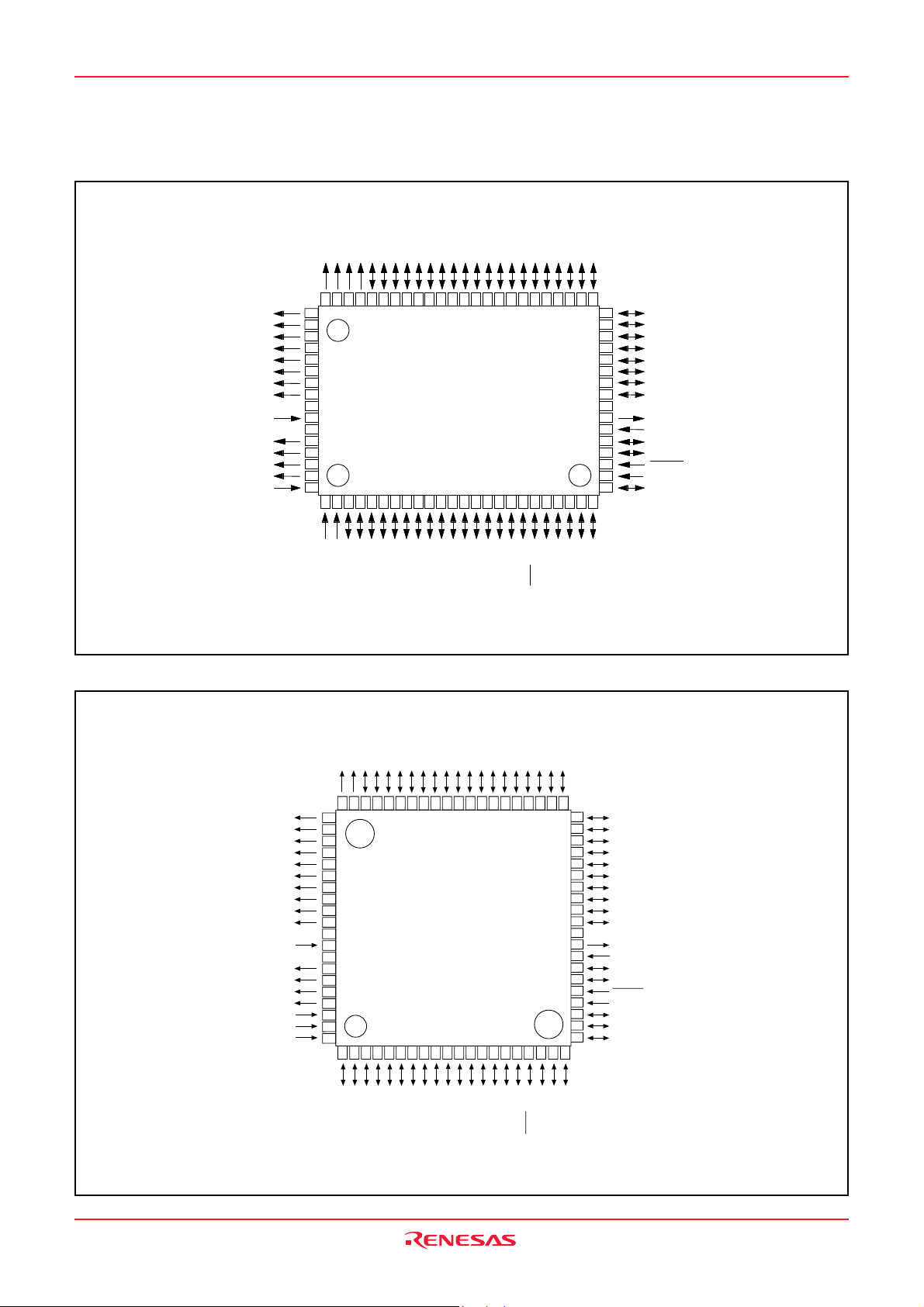
PIN CONFIGURATION (TOP VIEW)
8
9
G
G
S
E
S
E
E
S E G
7
6 5
S E G
S E G
S E G
S E G
S E G
SEG
S E G
V
A
C O M
C O M
C O M
C O M
V
C C
R E F
S
V
V L
6 6
6
5
6 7
4
6 8
6 9
3
7 0
2
1
7 1
7 2
0
7 3
7 4
7 5
S
3
7 6
2
7 7
1
7 8
0
7 9
8 0
3
1 234567891 01 112 1 314151 6171 819202 122 2 32 4
1
7
2
L
L
N
V
V
/
7
6
P
A
Package code : PRQP0080GB-A (80P6N-A) (80-pin plastic-molded QFP)
2
3
6
4
5
1
1
1
1
1
G
G
G
G
0
1
G
S
E
G
1
1
/
/
/
/
/
G
4
5
0
6
7
3
3
3
3
S E
S
0
S E
S E
S E
S E
S E
P
P
P
P
P
1
9
0
7
8
2
1
2
1
1
G
G
G
G
G
/
/
/
/
/
3
4
5
1
2
0
0
0
0
0
S E
S E
S E
S E
P
P
P
P
P
M 3 8 2 3 X G X - X X X F P
M 3 8 2 3 X G X F P
1
6
5
4
3
2
N
/
6
6
P
A
A
1
N
N
N
N
N
/
/
/
/
/
5
4
3
2
1
6
6
6
6
6
P
P
P
P
P
A
A
A
A
A
0
0
T
T
N
R
R
O
/
T
/
/
0
7
6
6
5
5
/
/
P
5
4
P
A D
P
U
R T
5
5
P
P
C N T
C N T
2
3
2
2
G
G
/
/
6
7
0
0
S E
S E
S E
P
P
3
1
0
T
P
P
/
/
/
1
3
2
5
5
5
P
I N
P
P
R T
8
5
6
7
9
0
4
2
2
2
G
G
G
/
/
/
1
2
0
1
1
1
S E
S E
S E
P
P
P
2
T
K
T
C
O
S
S
/
/
/
0
6
Y
5
4
P
I N
P
L
R
S
/
7
4
P
U
D
1
2
2
2
3
3
G
G
G
G
G
/
/
/
/
/
3
4
5
6
7
1
1
1
1
1
S E
S E
S E
S E
P
P
P
P
P
414243444546474849505152535455565758596061626364
40
39
38
37
36
35
34
33
32
31
30
29
28
27
26
25
0
1
D
D
T
T
X
X
T
R
/
/
/
/
5
4
3
2
4
4
4
4
P
P
P
P
I N
I N
P 20/ K W
P21/KW
P22/KW
P23/KW
P24/KW
P25/KW
P26/KW
P27/KW
V
SS
X
OUT
X
IN
P 70/ X
P 71/ X
R E S E T
P4
0
P41/φ
C O U T
C I N
0
1
2
3
4
5
6
7
Fig. 1 M3823XGX-XXXFP pin configuration
PIN CONFIGURATION (TOP VIEW)
SEG
SEG
SEG
SEG
SEG
SEG
SEG
SEG
SEG
SEG
V
AV
COM
COM
COM
COM
V
REF
V
V
V
61
9
62
8
63
7
64
6
65
5
66
4
67
3
68
2
1
69
70
0
CC
71
72
SS
73
3
74
2
75
1
76
0
77
L3
78
L2
79
L1
80
Package code : PLQP0080KB-A (80P6Q-A) (80-pin plastic-molded LQFP)
16
15
14
13
10
SEG
60
11
SEG
59
12
/SEG
4
P3
58
/SEG
5
P3
57
/SEG
6
P3
56
/SEG
7
P3
55
/SEG
0
P0
54
17
/SEG
1
P0
53
18
/SEG
2
P0
52
19
/SEG
3
P0
51
20
/SEG
4
P0
50
M3823XGX-XXXHP
M3823XGXHP
2
5
3
/AN
3
P6
6
2
/AN
2
P6
7
1
/AN
1
P6
8
0
/AN
0
P6
9
/ADT
7
P5
10
OUT
/T
6
P5
11
1
/CNTR
5
P5
1
7
/AN
7
P6
6
/AN
6
P6
3
5
/AN
5
P6
4
4
/AN
4
P6
22
21
/SEG
/SEG
6
5
P0
P0
49
48
13
12
0
/CNTR
4
P5
1
/RTP
3
P5
23
/SEG
7
P0
47
14
0
/RTP
2
P5
24
/SEG
0
P1
46
15
3
/INT
1
P5
25
/SEG
1
P1
45
16
2
/INT
0
P5
26
/SEG
2
P1
44
17
OUT
/S
RDY
/S
7
P4
27
/SEG
3
P1
43
18
CLK
/S
6
P4
28
/SEG
4
P1
42
19
D
X
/T
5
P4
29
/SEG
5
P1
41
40
39
38
37
36
35
34
33
32
31
30
29
28
27
26
25
24
23
22
21
20
D
X
/R
4
P4
P16/SEG
P17/SEG
P20/KW
P21/KW
P22/KW
P23/KW
P24/KW
P25/KW
P26/KW
P27/KW
V
SS
X
OUT
X
IN
P70/X
COUT
P71/X
CIN
RESET
P4
0
P41/φ
P42/INT
P43/INT
30
31
0
1
2
3
4
5
6
7
0
1
Fig. 2 M3823XGX-XXXHP pin configuration
Rev.2.02 Jun 19, 2007 page 2 of 73
REJ03B0146-0202
Page 3

3823 Group
Table 1 Performance overview
Parameter
Number of basic instructions
Instruction execution time
Oscillation frequency
Memory sizes ROM
RAM
Input port P34-P37, P40
I/O port P0-P2, P41-P47, P5, P6, P70, P71
Interrupt
Timer
Serial interface
A/D converter
Watchdog timer
ROM correction function
LCD drive control Bias
circuit
Main clock generating circuits
Sub-clock generating circuits
Power source voltage In frequency/2 mode (f(XIN) ≤ 10MHz)
Power dissipation In frequency/2 mode
Input/Output Input/Output withstand voltage
characteristics
Operating temperature range
Device structure
Package
Duty
Common output
Segment output
In frequency/2 mode (f(XIN) ≤ 8MHz)
In frequency/4 mode (f(XIN) ≤ 10MHz)
In frequency/4 mode (f(XIN) ≤ 8MHz)
In frequency/4 mode (f(XIN) ≤ 5MHz)
In frequency/8 mode (f(XIN) ≤ 10MHz)
In frequency/8 mode (f(XIN) ≤ 8MHz)
In frequency/8 mode (f(XIN) ≤ 5MHz)
In low-speed mode
In low-speed mode at XCIN
In low-speed mode at on-chip oscillator
Output current
Function
71
0.4 µs (Minimum instruction, f(XIN) 10 MHz, High-speed mode)
10 MHz (Maximum)
16 K to 60 K bytes
640 to 2560 bytes
4-bit ✕ 1, 1-bit ✕ 1
(4 pins sharing SEG)
8-bit ✕ 5, 7-bit ✕ 1, 2 bit ✕ 1
(16 pins sharing SEG)
17 sources, 16 vectors (includes key input interrupt)
8-bit ✕ 3, 16-bit ✕ 2
8-bit ✕ 1 (UART or Clock-synchronized)
10-bit ✕ 8 channels or 8 bit ✕ 8 channels
8-bit ✕ 1
32 bytes ✕ 2 blocks
1/2, 1/3
2, 3, 4
4
32
Built-in feedback resistor
(connect to external ceramic rasonator or quartz-crystal oscillator)
Built-in feedback resistor
(connect to external quartz-crystal oscillator or on-chip oscillator)
4.5 to 5.5V
4.0 to 5.5V
2.5 to 5.5V
2.0 to 5.5V
1.8 to 5.5V
2.5 to 5.5V
2.0 to 5.5V
1.8 to 5.5V
1.8 to 5.5V
Std. 18 mW (Vcc = 5V, f(XIN) = 8MHz, Ta = 25 °C)
Std. 18 µW (Vcc = 2.5V, f(XIN) = stopped, f(XCIN) = 32kHz, Ta = 25 °C)
Std. 35 µW (Vcc = 2.5V, f(XIN) = stopped, f(XCIN) = stopped, Ta = 25 °C)
VCC
10mA
-20 to 85 °C
CMOS sillicon gate
80-pin plastic molded LQFP/QFP
Rev.2.02 Jun 19, 2007 page 3 of 73
REJ03B0146-0202
Page 4
3823 Group
K
e y o n w a k e u
p
R
e a l t i m e p o r t f u n c t i o
n
I
N
T
2
,
I N
T
3
C
N T
R
0
,
C N T
R
1
O
U
T
A
D
T
I
N
T0,
I N
T
1
φ
,
X
C
I
N
R
T
P
0
,
R T
P
1
D
a t a b u
s
C
P
U
A
X
Y
S
C
H
C
L
P
S
E
S
E
T
V
C
C
V
S
S
R
e s e t I n p u
t
5
V
)
(
0 V
)
O
M
R
A
M
L
C D d i s p l a y
R
A M
(
1 6 b y t e s
)
2
5
7
1
3
0
/
O
P
o
r
t
P
5
P
4 ( 8
)
/
O
P
o
r
t
P
4
I
/ O P o r t P
2
2
(
8
)
I
/ O P o r t P
0
0
(
8
)
I
/ O P o r t P
1
1
(
8
)
P
6 ( 8
)
I
n p u t P o r t P
3
3
(
4
)
I
/ O P o r t P
6
P
5 ( 8
)
I
/ O P o r t P
7
7
(
2
)
8
0
7
9
8
7
6
5
7
4
7
0
6
9
6
8
7
6
5
4
3
2
6
1
6
0
5
9
4
7
4
8
4
9
5
0
5
1
5
2
3
5
4
3
9
0
1
4
2
4
3
4
4
4
5
4
6
3
1
3
2
3
3
4
3
5
3
6
7
8
5
5
6
5
7
8
9
2
0
2
1
2
2
3
2
4
1
7
1
8
2
6
2
7
1
2
4
5
7
7
3
2
1
0
1
1
1
2
1
3
1
4
1
5
6
C
l o c k g e n e r a t i n
g
c
i r c u i
t
M
a i n C l o c k n p u t
X
I
N
M
a i n C l o c k
O
u t p u t
X
O
U
T
X
C
O
U
T
u b - C l o c k u t p u
t
X
C
I
N
S
u b - C l o c k
I
n p u t
I
/
O
(
8
)
R
E
F
A
V
S
S
(
0
V
)
A
/ D c o n v e r t e
r
(
1
0
/
8
)
i
m
e
r
X
(
1
6
)
T
i m e r Y ( 1 6
)
i
m
e
r
1
(
8
)
T
i m e r 2 ( 8
)
T
i m e r 3 ( 8
)
C
D
r
i
v
e
c
o
n
t
r
o
l
i
r
c
u
i
t
V
L
1
V
L
2
V
L
3
C
O
M
0
C
O
M
1
C
O
M
2
C
O
M
3
E
G
0
E
G
1
E
G
2
E
G
3
E
G
4
S
E
G
5
S
E
G
6
S
E
G
7
S
E
G
8
S
E
G
9
S
E
G
1
0
S
E
G
1
1
φ
C
I
N
C
O
U
T
2
8
2
9
O
n - c h i
p
o
s c i l l a t o
r
R
O M o r r e c t i o n u n c t i o
n
W
a t c h d o
g
t
i m e
r
R
e s e
t
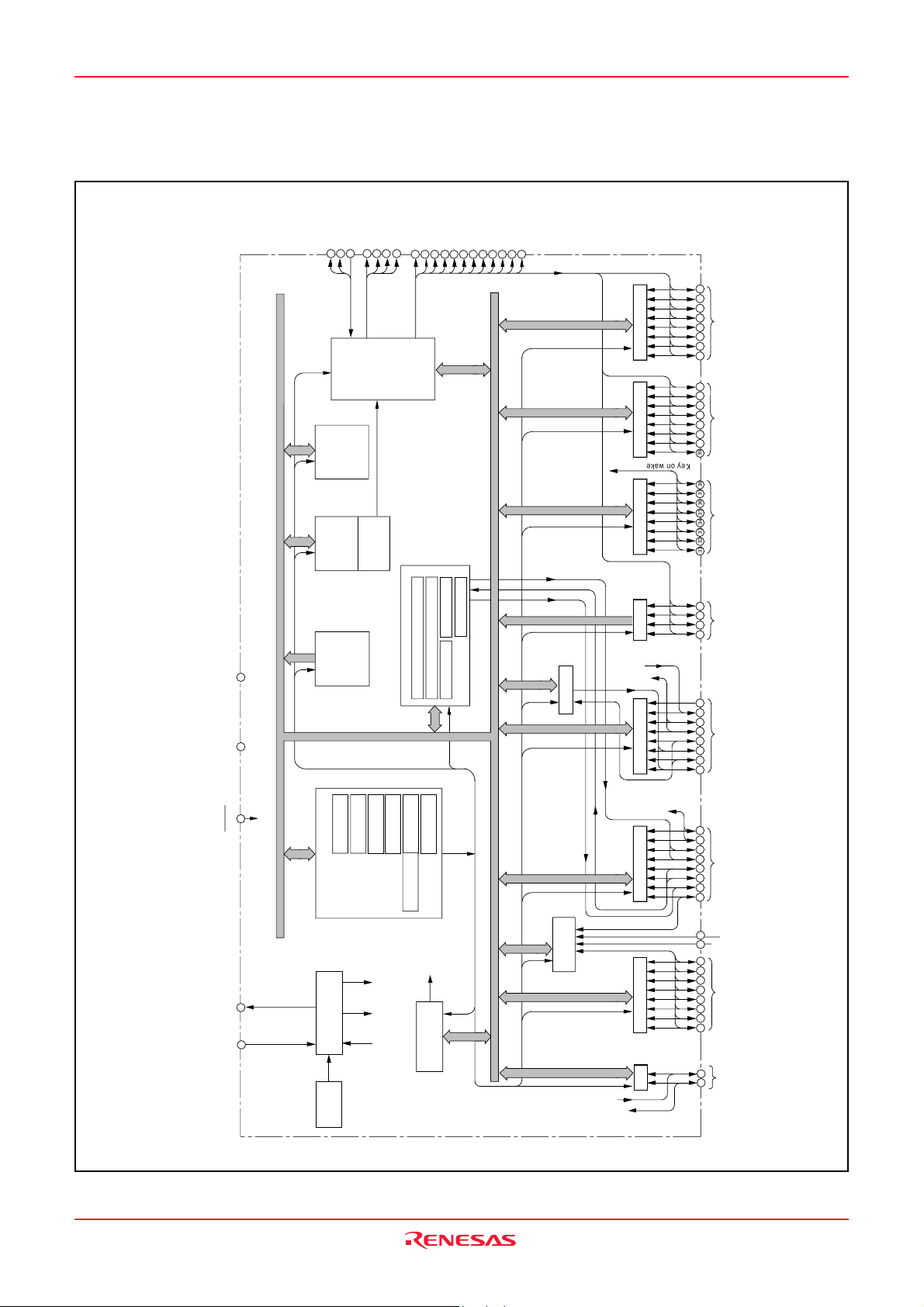
FUNCTIONAL BLOCK DIAGRAM (Package type : PLQP0080KB-A)
Fig. 3 Functional block diagram
Rev.2.02 Jun 19, 2007 page 4 of 73
REJ03B0146-0202
Page 5

3823 Group
PIN DESCRIPTION
Table 2 Pin description (1)
VCC, VSS
VREF
AVSS
RESET
XIN
XOUT
VL1–VL3
COM0–COM
SEG0–SEG
P00/SEG16–
P07/SEG23
P10/SEG24–
P17/SEG31
P20/KW0 –
P27/KW7
P34/SEG12 –
P37/SEG
15
FunctionPin Name
Power source •Apply voltage of power source to VCC, and 0 V to VSS. (For the limits of VCC, refer to “Recom-
Analog reference voltage
Analog power
source
Reset input
Clock input
Clock output
LCD power
source
Common output
3
11
Segment output
I/O port P0
I/O port P1
I/O port P2
Input port P3
mended operating conditions”).
•Reference voltage input pin for A/D converter.
•GND input pin for A/D converter.
•Connect to VSS.
•Reset input pin for active “L”.
•Input and output pins for the main clock generating circuit.
•Feedback resistor is built in between XIN pin and XOUT pin.
•Connect a ceramic resonator or a quartz-crystal oscillator between the XIN and XOUT pins to set
the oscillation frequency.
•If an external clock is used, connect the clock source to the XIN pin and leave the XOUT pin open.
•This clock is used as the oscillating source of system clock.
•Input 0 ≤ VL1 ≤ VL2 ≤ VL3 voltage.
•Input 0 – VL3 voltage to LCD.
•LCD common output pins.
•COM2 and COM3 are not used at 1/2 duty ratio.
•COM3 is not used at 1/3 duty ratio.
•LCD segment output pins.
•8-bit I/O port.
•CMOS compatible input level.
•CMOS 3-state output structure.
•I/O direction register allows each port to be individually
programmed as either input or output.
•Pull-down control is enabled.
•8-bit I/O port.
•CMOS compatible input level.
•CMOS 3-state output structure.
•I/O direction register allows each pin to be individually
programmed as either input or output.
•Pull-up control is enabled.
•4-bit input port.
•CMOS compatible input level.
•Pull-down control is enabled.
Function except a port function
•LCD segment output pins
•Key input (key-on wake-up) interrupt
input pins
•LCD segment output pins
Rev.2.02 Jun 19, 2007 page 5 of 73
REJ03B0146-0202
Page 6

3823 Group
Table 3 Pin description (2)
P40
P41/φ
P42/INT0,
P43/INT1
P44/RXD,
P45/TXD,
P46/SCLK,
P47/SRDY/SOUT
P50/INT2,
P51/INT3
P52/RTP0,
P53/RTP1
P54/CNTR0,
P55/CNTR1
P56/TOUT
P57/ADT
P60/AN0–
P67/AN7
P70/XCOUT,
P71/XCIN
Name
Input port P4
I/O port P4
I/O port P5
I/O port P6
I/O port P7
FunctionPin
•1-bit Input port.
•CMOS compatible input level.
•7-bit I/O port.
•CMOS compatible input level.
•CMOS 3-state output structure.
•I/O direction register allows each pin to be individually
programmed as either input or output.
•Pull-up control is enabled.
•8-bit I/O port.
•CMOS compatible input level.
•CMOS 3-state output structure.
•I/O direction register allows each pin to be individually
programmed as either input or output.
•Pull-up control is enabled.
•8-bit I/O port.
•CMOS compatible input level.
•CMOS 3-state output structure.
•I/O direction register allows each pin to be individually
programmed as either input or output.
•Pull-up control is enabled.
•2-bit I/O port.
•CMOS compatible input level.
•CMOS 3-state output structure.
•I/O direction register allows each pin to be individually
programmed as either input or output.
•Pull-up control is enabled.
Function except a port function
•QzROM program power pin
•φ clock output pin
•Interrupt input pins
•Serial interface function pins
•Interrupt input pins
•Real time port function pins
•Timer X, Y function pins
•Timer 2 output pins
•A/D trigger input pins
•A/D conversion input pins
•Sub-clock generating circuit I/O pins.
(Connect a resonator. External clock
cannot be used.)
Rev.2.02 Jun 19, 2007 page 6 of 73
REJ03B0146-0202
Page 7

3823 Group
PART NUMBERING
Product M38234 G 6 -XXX FP
Package code
FP : PRQP0080GB-A package
HP : PLQP0080KB-A package
ROM number
Omitted in the shipped in blank version.
ROM/PROM size
1 : 4096 bytes
2 : 8192 bytes
3 : 12288 bytes
4 : 16384 bytes
5 : 20480 bytes
6 : 24576 bytes
7 : 28672 bytes
8 : 32768 bytes
The first 128 bites and the last 2 bytes of ROM are
reserved areas ; they cannot be used.
9 : 36864 bytes
A : 40960 bytes
B : 45056 bytes
C : 49152 bytes
D : 53248 bytes
E : 57344 bytes
F : 61440 bytes
Memory type
G : QzROM version
RAM size
0 : 192 bytes
1 : 256 bytes
2 : 384 bytes
3 : 512 bytes
4 : 640 bytes
5 : 768 bytes
6 : 896 bytes
7 : 1024 bytes
8 : 1536 bytes
9 : 2048 bytes
A : 2560 bytes
Fig. 4 Part numbering
Rev.2.02 Jun 19, 2007 page 7 of 73
REJ03B0146-0202
Page 8
3823 Group
GROUP EXPANSION
Mitsubishi plans to expand the 3823 group as follows:
Memory Type
Support for QzROM version.
Memory Size
ROM size ........................................................... 16 K to 60 K bytes
RAM size ............................................................ 640 to 2560 bytes
Memory Expansion Plan
ROM size (bytes)
60K
56K
48K
40K
32K
28K
24K
20K
16K
Mass production
M38235G6
Mass production
M38234G4
Package
PRQP0080GB-A........................ 0.8 mm-pitch plastic molded QFP
PLQP0080KB-A....................... 0.5 mm-pitch plastic molded LQFP
Mass production
M3823AGF
Mass production
M38239GC
Mass production
M38238G8
12K
8K
4K
192
Fig. 5 Memory expansion plan
256 384 512 640 768 896
RAM size (bytes)
1,024
1,536 2,048
2,560
Rev.2.02 Jun 19, 2007 page 8 of 73
REJ03B0146-0202
Page 9
3823 Group
Currently products are listed below.
Table 4 List of products
Part No.
M3823AGF-XXXFP
M3823AGF-XXXHP
M3823AGFFP
M3823AGFHP
M38239GC-XXXFP
M38239GC-XXXHP
M38239GCFP
M38239GCHP
M38238G8-XXXFP
M38238G8-XXXHP
M38238G8FP
M38238G8HP
M38235G6-XXXFP
M38235G6-XXXHP
M38235G6FP
M38235G6HP
M38234G4-XXXFP
M38234G4-XXXHP
M38234G4FP
M38234G4HP
Note 1: RAM size includes RAM for LCD display and ROM corrections.
Note 2: RAM size includes RAM for LCD display.
ROM size (bytes)
size for User in ( )
61440
(61310)
49152
(49022)
32768
(32638)
24576
(24446)
16384
(16254)
ROM
RAM size
(bytes)
2560
(Note 1)
2048
(Note 2)
1536
(Note 2)
768
(Note 2)
640
(Note 2)
PRQP0080GB-A
PLQP0080KB-A
PRQP0080GB-A
PLQP0080KB-A
PRQP0080GB-A
PLQP0080KB-A
PRQP0080GB-A
PLQP0080KB-A
PRQP0080GB-A
PLQP0080KB-A
PRQP0080GB-A
PLQP0080KB-A
PRQP0080GB-A
PLQP0080KB-A
PRQP0080GB-A
PLQP0080KB-A
PRQP0080GB-A
PLQP0080KB-A
PRQP0080GB-A
PLQP0080KB-A
RemarksPackage
Blank
Blank
Blank
Blank
Blank
Blank
Blank
Blank
Blank
Blank
Rev.2.02 Jun 19, 2007 page 9 of 73
REJ03B0146-0202
Page 10
3823 Group
FUNCTIONAL DESCRIPTION
CENTRAL PROCESSING UNIT (CPU)
The 3823 group uses the standard 740 family instruction set. Refer to the table of 740 family addressing modes and machine
instructions or the 740 Family Software Manual for details on the
instruction set.
Machine-resident 740 family instructions are as follows:
The FST and SLW instruction cannot be used.
The STP, WIT, MUL, and DIV instruction can be used.
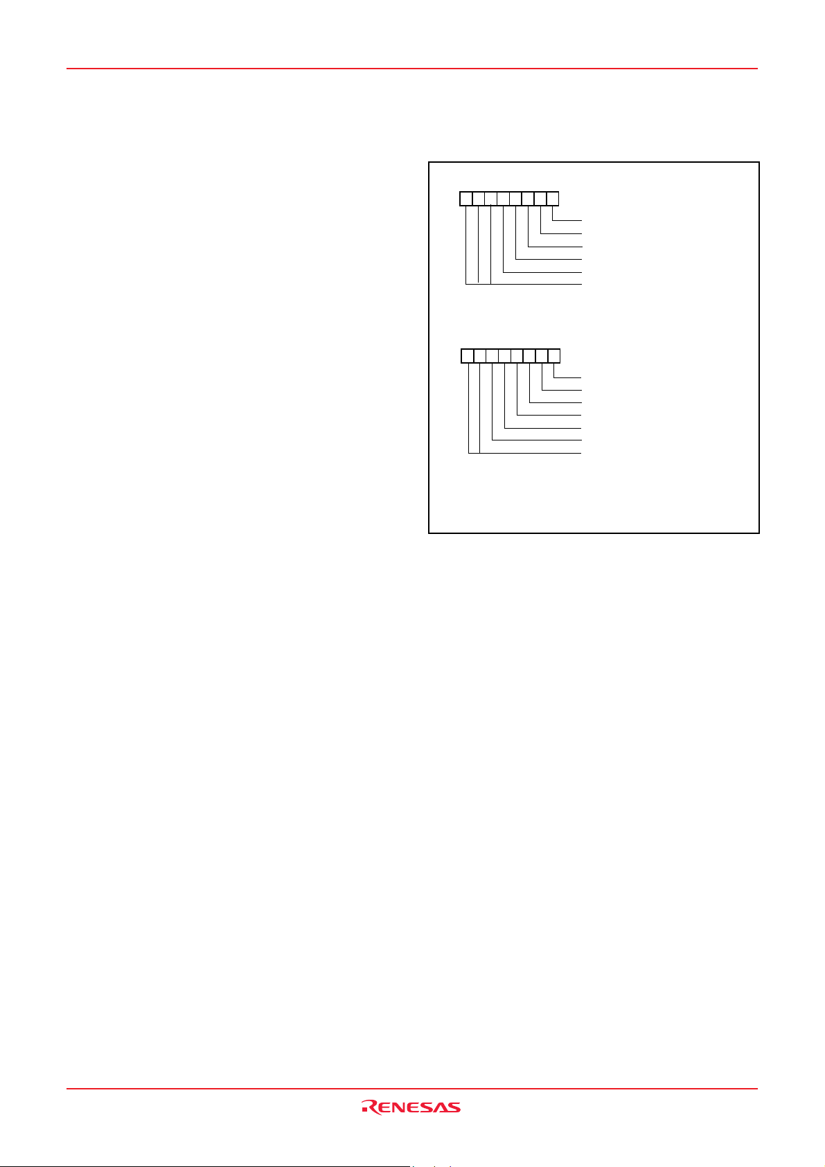
The central processing unit (CPU) has six registers. Figure 6
shows the 740 Family CPU register structure.
[Accumulator (A)]
The accumulator is an 8-bit register. Data operations such as data
transfer, etc., are executed mainly through the accumulator.
[Index Register X (X)]
The index register X is an 8-bit register. In the index addressing
modes, the value of the OPERAND is added to the contents of
register X and specifies the real address.
[Index Register Y (Y)]
The index register Y is an 8-bit register. In partial instruction, the
value of the OPERAND is added to the contents of register Y and
specifies the real address.
[Stack Pointer (S)]
The stack pointer is an 8-bit register used during subroutine calls
and interrupts. This register indicates start address of stored area
(stack) for storing registers during subroutine calls and interrupts.
The low-order 8 bits of the stack address are determined by the
contents of the stack pointer. The high-order 8 bits of the stack address are determined by the stack page selection bit. If the stack
page selection bit is “0” , the high-order 8 bits becomes “0016”. If
the stack page selection bit is “1”, the high-order 8 bits becomes
“0116”.
The operations of pushing register contents onto the stack and
popping them from the stack are shown in Figure 7.
Store registers other than those described in Table 4 with program
when the user needs them during interrupts or subroutine calls.
[Program Counter (PC)]
The program counter is a 16-bit counter consisting of two 8-bit
registers PCH and PCL. It is used to indicate the address of the
next instruction to be executed.
b7
b0
A Accumulator
b7
b0
X Index register X
b7
b0
Y Index register Y
b7 b0
S Stack pointer
b7b15 b0
H
PC
L
Program counterPC
b7 b0
N VTBDIZC Processor status register (PS)
Carry flag
Zero flag
Interrupt disable flag
Decimal mode flag
Break flag
Index X mode flag
Overflow flag
Negative flag
Fig. 6 740 Family CPU register structure
Rev.2.02 Jun 19, 2007 page 10 of 73
REJ03B0146-0202
Page 11
3823 Group
e
O n - g o i n g R o u t i n
P u s h r e t u r n a d d r e s s
o n s t a c k
P O P re t u r n
a d d r e s s f r o m s t a c k
I n t e r r u p t r e q u e s t
M ( S )( P CH)
S ) –
( S )
M ( S )( P CL)
S ) –
( S )
S u b r o u t i n e
E x e c u t e R T S
S ) +
( S )
( P CL)M ( S )
S ) +
( S )
( P CH)M ( S )
( N o t e )
(
(
1
(
(
M ( S )( P CH)
E x e c u t e J S R
1
1
1
( S )
( S ) – 1
M ( S )( P CL)
S ) –
( S )
(
M ( S )( P S )
S ) –
( S )
(
I n t e r r u p t
S e r v i c e R o u t i n e
E x e c u t e R T I
S ) +
( S )
(
( P S )M ( S )
S ) +
( S )
(
( P CL)M ( S )
S ) +
( S )
(
P u s h r e t u r n a d d r e s s
o n s t a c k
1
P u s h c o n t e n t s o f p r o c e s s o r
s t a t u s r e g i s t e r o n s t a c k
1
I F l a g i s s e t f r o m “ 0 ” t o “ 1 ”
F e t c h t h e j u m p v e c t o r
1
P O P c o n t e n t s o f
p r o c e s s o r s t a t u s
r e g i s t e r f r o m s t a c k
1
P O P r e t u r n
a d d r e s s
1
f r o m s t a c k
( P CH)M ( S )
N o t e: C o n d i t i o n f o r a c c e p t a n c e o f a n i n t e r r u p t I n t e r r u p t e n a b l e f l a g i s “ 1 ”
Fig. 7 Register push and pop at interrupt generation and subroutine call
Table 5 Push and pop instructions of accumulator or processor status register
Push instruction to stack
Accumulator
Processor status register
I n t e r r u p t d i s a b l e f l a g i s “ 0 ”
PHA
PHP
Pop instruction from stack
PLA
PLP
Rev.2.02 Jun 19, 2007 page 11 of 73
REJ03B0146-0202
Page 12
3823 Group
[Processor status register (PS)]
The processor status register is an 8-bit register consisting of 5
flags which indicate the status of the processor after an arithmetic
operation and 3 flags which decide MCU operation. Branch operations can be performed by testing the Carry (C) flag , Zero (Z) flag,
Overflow (V) flag, or the Negative (N) flag. In decimal mode, the Z,
V, N flags are not valid.
•Bit 0: Carry flag (C)
The C flag contains a carry or borrow generated by the arithmetic
logic unit (ALU) immediately after an arithmetic operation. It can
also be changed by a shift or rotate instruction.
•Bit 1: Zero flag (Z)
The Z flag is set if the result of an immediate arithmetic operation
or a data transfer is “0”, and cleared if the result is anything other
than “0”.
•Bit 2: Interrupt disable flag (I)
The I flag disables all interrupts except for the interrupt
generated by the BRK instruction.
Interrupts are disabled when the I flag is “1”.
•Bit 3: Decimal mode flag (D)
The D flag determines whether additions and subtractions are
executed in binary or decimal. Binary arithmetic is executed when
this flag is “0”; decimal arithmetic is executed when it is “1”.
Decimal correction is automatic in decimal mode. Only the ADC
and SBC instructions can be used for decimal arithmetic.
•Bit 4: Break flag (B)
The B flag is used to indicate that the current interrupt was
generated by the BRK instruction. The BRK flag in the processor
status register is always “0”. When the BRK instruction is used to
generate an interrupt, the processor status register is pushed
onto the stack with the break flag set to “1”.
•Bit 5: Index X mode flag (T)
When the T flag is “0”, arithmetic operations are performed
between accumulator and memory. When the T flag is “1”, direct
arithmetic operations and direct data transfers are enabled
between memory locations.
•Bit 6: Overflow flag (V)
The V flag is used during the addition or subtraction of one byte
of signed data. It is set if the result exceeds +127 to -128. When
the BIT instruction is executed, bit 6 of the memory location
operated on by the BIT instruction is stored in the overflow flag.
•Bit 7: Negative flag (N)
The N flag is set if the result of an arithmetic operation or data
transfer is negative. When the BIT instruction is executed, bit 7 of
the memory location operated on by the BIT instruction is stored
in the negative flag.
Table 6 Set and clear instructions of each bit of processor status register
Set instruction
Clear instruction
C flag
SEC
CLC
Z flag
–
–
I flag
SEI
CLI
D flag
SED
CLD
B flag
–
–
T flag
SET
CLT
V flag
–
CLV
N flag
–
–
Rev.2.02 Jun 19, 2007 page 12 of 73
REJ03B0146-0202
Page 13
3823 Group
[CPU Mode Register (CPUM)] 003B16
The CPU mode register contains the stack page selection bit and
the internal system clock selection bit.
The CPU mode register is allocated at address 003B
16.
b7
Note 1: In low speed mode (X
switch bit is set to "0".
2: In frequency/2/4/8 mode, X
3: When the system clock φ is divided by 4 of f(X
in the CPU mode extension register to “1”.
4: When using the on-chip oscillator in low-speed mode, set the bit 7 in the CPU mode register to “1” after setting the
bit 0 in the CPU mode extension register to “1”.
Fig. 8 Structure of CPU mode register
b0
CPU mode register
(CPUM (CM) : address 003B
Processor mode bits
b1 b0
0 0 : Single-chip mode
0 1 :
1 0 :
1 1 :
Stack page selection bit
0 : 0 page
1 : 1 page
Not used (returns “1” when read)
(Do not write “0” to this bit)
C
Port X
0 : I/O port function (stop oscillating)
1 : X
Main clock (X
0 : Oscillating
1 : Stopped
Main clock division ratio selection bit
0 : f(X
1 : f(X
Internal system clock selection bit
0 : X
1 : X
CIN
is selected as the system clock φ), X
IN-XOUT
oscillation does not stop even if the main clock (XIN-X
IN
), set the bit 6 in the CPU mode register to “0” after setting the bit 1
16
)
Not available
switch bit
(Note 1)
CIN–XCOUT
oscillating function
IN
–
X
OUT
) stop bit (Note 2)
IN
)/2 (frequency/2 mode), or
IN
)/8 (frequency/8 mode)
IN–XOUT
selected (frequency/2/4/8 mode)
CIN–XCOUT,
or on-chip oscillator selected (low-speed mode) (Note 4)
CIN-XCOUT
f(X
IN
)/4 (frequency/4 mode) (Note 3)
oscillation does not stop even if the port XC
OUT
) stop bit is set to "1".
[CPU Mode Extension Register (EXPCM)] 002B
16
f(XIN) divided by 4 for the system clock f and the on-chip oscillator
for the system clock f in low-speed mode can be selected by setting the CPU mode extension register. When the system clock f is
divided by 4 of f(XIN), set the bit 6 in the CPU mode register to “0”
after setting the bit 1 in the CPU mode extension register to “1”.
When using the on-chip oscillator in low-speed mode, set the bit 7
in the CPU mode register to “1” after setting the bit 0 in the CPU
mode extension register to “1”.
Rev.2.02 Jun 19, 2007 page 13 of 73
REJ03B0146-0202
b7
Note
1 : The on-chip oscillator is selected for the operation clock in low-speed mod regardless
CIN-XCOUT
of X
2 : Valid only when the main clock division ratio selection bit (bit 6 in the CPU mode
register) is set to "0".
When "1" (frequency/8 mode) is selected for the main clock division ratio selection bit or
when the internal system clock selection bit is set to 1, set "0" to the frequency/4 mode
control bit.
.
b0
CPU mode extension register
(EXPCM : address 002B
On-chip oscillator control bit
0 : On-chip oscillator not used
(On -chip oscillator sotpping)
1 : On-chip oscillator used (Note 1)
(On -chip oscillator oscillating)
Frequency/4 mode control bit (Note 2)
0 : Frequency/2 mode φ = f(X
1 : Frequency/4 mode φ = f(X
Not used (returns “0” when read)
(Do not write “1” to this bit)
Fig. 9 Structure of CPU mode extension register
16
)
IN
)/2
IN
)/4
Page 14
3823 Group
B F
RAM
R A M
A d d
4
6
8
2
0
C
C
R O M
R O M
A d d
A d d
FF
F F D C
FFFE
FFFF
XXXX
ZZZZ
RAM
R O M
RAM f
ROM
SFR
N
d
I
R
Z
S
R
LCD displ
RAM
R A M
R A M
F
A
A
F
Y Y Y Y
MEMORY
Special Function Register (SFR) Area
The Special Function Register area in the zero page contains control registers such as I/O ports and timers.
RAM
RAM is used for data storage and for stack area of subroutine
calls and interrupts.
ROM
The first 128 bytes and the last 2 bytes of ROM are reserved for
device testing and the rest is user area for storing programs.
Interrupt Vector Area
The interrupt vector area contains reset and interrupt vectors.
Zero Page
The 256 bytes from addresses 000016 to 00FF16 are called the
zero page area. The internal RAM and the special function register (SFR) are allocated to this area.
The zero page addressing mode can be used to specify memory
and register addresses in the zero page area. Access to this area
with only 2 bytes is possible in the zero page addressing mode.
Special Page
The 256 bytes from addresses FF0016 to FFFF16 are called the
special page area. The special page addressing mode can be
used to specify memory addresses in the special page area.
Access to this area with only 2 bytes is possible in the special
page addressing mode.
ROM Code Protect Address
“0016” is written into ROM code protect address (other than the
user ROM area) when selecting the protect bit write by using a serial programmer or selecting protect enabled for writing shipment
by Renesas Technology corp.. When “0016” is set to the ROM
code protect address, the protect function is enabled, so that reading or writing from/to QzROM is disabled by a serial programmer.
As for the QzROM product in blank, the ROM code is protected by
selecting the protect bit write at ROM writing with a serial programmer.
As for the QzROM product shipped after writing, “0016” (protect
enabled) or “FF16” (protect disabled) is written into the ROM code
protect address when Renesas Technology corp. performs writing.
The writing of “0016" or “FF16” can be selected as ROM option
setup (“MASK option” written in the mask file converter) when ordering.
area
s i z
( b y t e s )
6 4 0
7 6 8
1 5 3 6
2 0 4 8
2 5 6 0
a r e
s i z
( b y t e s )
1 6 3 8
2 4 5 7
3 2 7 6
4 9 1 5
6 1 4 4
r e s s
e
a
r e s
e
X X X X
0 2
0 3 3 F
0 6 3 F
0 8 3 F
0 A3 F
Y Y Y Y
0 0
A 0 0 0
8 0 0 0
4 0 0 0
10 0 0
1 6
1 6
1 6
1 6
1 6
1 6
r e s
s
1 6
1 6
0
1 6
1 6
1 6
1 6
Z Z Z Z
0 8
A 0 8 0
8 0 8 0
4 0 8 0
10 8 0
s
1 6
1 6
0
1 6
1 6
1 6
1 6
0000
0040
0050
0100
0A40
16
16
16
16
16
16
1 6
e s e r v e d R O M a r e
16
00
16
1 6
16
e s e r v e d R O M a r e
16
area
ay
area
or
correction
o t u s e
nterru pt vecto r area
ero page
0A00
16
1 f o r R O M c o r r e c t i o
0A1
16
2
0
1 6
0
2 f o r R O M c o r r e c t i o
3
0
1 6
a
p e c i a l p a g
a
e
n
n
Fig. 10 Memory map diagram
Rev.2.02 Jun 19, 2007 page 14 of 73
REJ03B0146-0202
Page 15

3823 Group
A
B
C
D
E
F
A
B
C
D
E
F
A
B
C
D
E
F
A
B
C
D
E
F
I
)
T i
)
T i
)
I
(INTEDGE)
C P U
)
I
(IREQ1)
I
(IREQ2)
I
)
T i
)
T i
)
T i
)
T i
)
T i
)
T i
)
T i
)
Ti
M)
(CKOUT)
S
)
LCD
(LM)
A D
)
A D
)
P
)
P
)
P
)
P
)
P
)
P
)
P
)
P
)
P
)
P
)
P
)
P
)
P
)
P
)
S
)
Serial I/O
(SIO1CON)
UART
(UARTCON)
Baud
(BRG)
P U L L
)
P U L L
)
T
( T B
)
P
)
R O M
)
R O M
)
R O M
)
R O M
)
R O M
)
T
)
T
)
C P U
)
T
)
RRF
(RRFR)
Periph
(EXP)
A D
)
W
(WDT)
N
0 0 0 01
0 0 0 11
0 0 0 21
0 0 0 31
0 0 0 41
0 0 0 51
0 0 0 61
0 0 0 71
0 0 0 81
0 0 0 91
0 0 0
0 0 0
0 0 0
0 0 0
000
0 0 0
0 0 1 01
0 0 1 11
0 0 1 21
0 0 1 31
0 0 1 41
0 0 1 51
0 0 1 61
0 0 1 71
001816
001916
001
0 0 1
0 0 1
001
001
0 0 1
o r t P 0 r e g i s t e r ( P 0
6
o r t P 0 d i r e c t i o n r e g i s t e r ( P 0 D
6
o r t P 1 r e g i s t e r ( P 1
6
o r t P 1 d i r e c t i o n r e g i s t e r ( P 1 D
6
o r t P 2 r e g i s t e r ( P 2
6
o r t P 2 d i r e c t i o n r e g i s t e r ( P 2 D
6
o r t P 3 r e g i s t e r ( P 3
6
6
o r t P 4 r e g i s t e r ( P 4
6
o r t P 4 d i r e c t i o n r e g i s t e r ( P 4 D
6
o r t P 5 r e g i s t e r ( P 5
1 6
o r t P 5 d i r e c t i o n r e g i s t e r ( P 5 D
1 6
o r t P 6 r e g i s t e r ( P 6
1 6
o r t P 6 d i r e c t i o n r e g i s t e r ( P 6 D
1 6
o r t P 7 r e g i s t e r ( P 7
16
o r t P 7 d i r e c t i o n r e g i s t e r ( P 7 D
1 6
c o r r e c t i o n a d d r e s s 1 h i g h - o r d e r r e g i s t e r ( R C A 1 H
6
c o r r e c t i o n a d d r e s s 1 l o w - o r d e r r e g i s t e r ( R C A 1 L
6
c o r r e c t i o n a d d r e s s 2 h i g h - o r d e r r e g i s t e r ( R C A 2 H
6
c o r r e c t i o n a d d r e s s 2 l o w - o r d e r r e g i s t e r ( R C A 2 L
6
c o r r e c t i o n e n a b l e r e g i s t e r ( R C R
6
6
r e g i s t e r A ( P U L L A
6
r e g i s t e r B ( P U L L B
6
r a n s m i t / R e c e i v e b u f f e r r e g i s t e
e r i a l I / O s t a t u s r e g i s t e r ( S I O S T S
16
1 6
1 6
16
16
1 6
control register
control register
rate generator
m e r X l o w - o r d e r r e g i s t e r ( T X L
0 0 2 01
6
m e r X h i g h - o r d e r r e g i s t e r ( T X H
0 0 2 11
6
m e r Y l o w - o r d e r r e g i s t e r ( T Y L
0 0 2 21
6
m e r Y h i g h - o r d e r r e g i s t e r ( T Y H
0 0 2 31
6
m e r 1 r e g i s t e r ( T 1
0 0 2 41
6
m e r 2 r e g i s t e r ( T 2
0 0 2 51
6
m e r 3 r e g i s t e r ( T 3
0 0 2 61
6
m e r X m o d e r e g i s t e r ( T X M
0 0 2 71
6
m e r Y m o d e r e g i s t e r ( T Y M
0 0 2 81
6
0 0 2 91
6
0 0 2
0 0 2
002
002
002
0 0 2
0 0 3 01
0 0 3 11
0 0 3 21
0 0 3 31
0 0 3 41
0 0 3 51
0 0 3 61
/ R B
r
0 0 3 71
003816
003916
003
0 0 3
003
003
003
0 0 3
mer 12 3 mode register (T123
1 6
φ output control register
m o d e e x p a n s i o n r e g i s t e r ( E X P C M
1 6
e m p o r a r y d a t a r e g i s t e r 0 ( T D 0
16
e m p o r a r y d a t a r e g i s t e r 1 ( T D 1
16
e m p o r a r y d a t a r e g i s t e r 2 ( T D 2
16
1 6
register
6
6
6
6
6
6
6
6
eral function expansion register
c o n t r o l r e g i s t e r ( A D C O N
c o n v e r s i o n h i g h - o r d e r r e g i s t e r ( A D H
c o n v e r s i o n l o w - o r d e r r e g i s t e r ( A D L
atchdog timer register
e g m e n t o u t p u t e n a b l e r e g i s t e r ( S E G
mode register
16
nterrupt edge selection register
m o d e r e g i s t e r ( C P U M
1 6
16
nterrupt request register 1
16
nterrupt request register 2
n t e r r u p t c o n t r o l r e g i s t e r 1 ( I C O N 1
16
n t e r r u p t c o n t r o l r e g i s t e r 2 ( I C O N 2
1 6
o t e : D o n o t a c c e s s t o t h e S F R a r e a i n c l u d i n g n o t h i n g
Fig. 11 Memory map of special function register (SFR)
Rev.2.02 Jun 19, 2007 page 15 of 73
REJ03B0146-0202
.
Page 16
3823 Group
P
PULL
A
b7b
P
D i
PULL
B
b7b
N
PULL
PULL
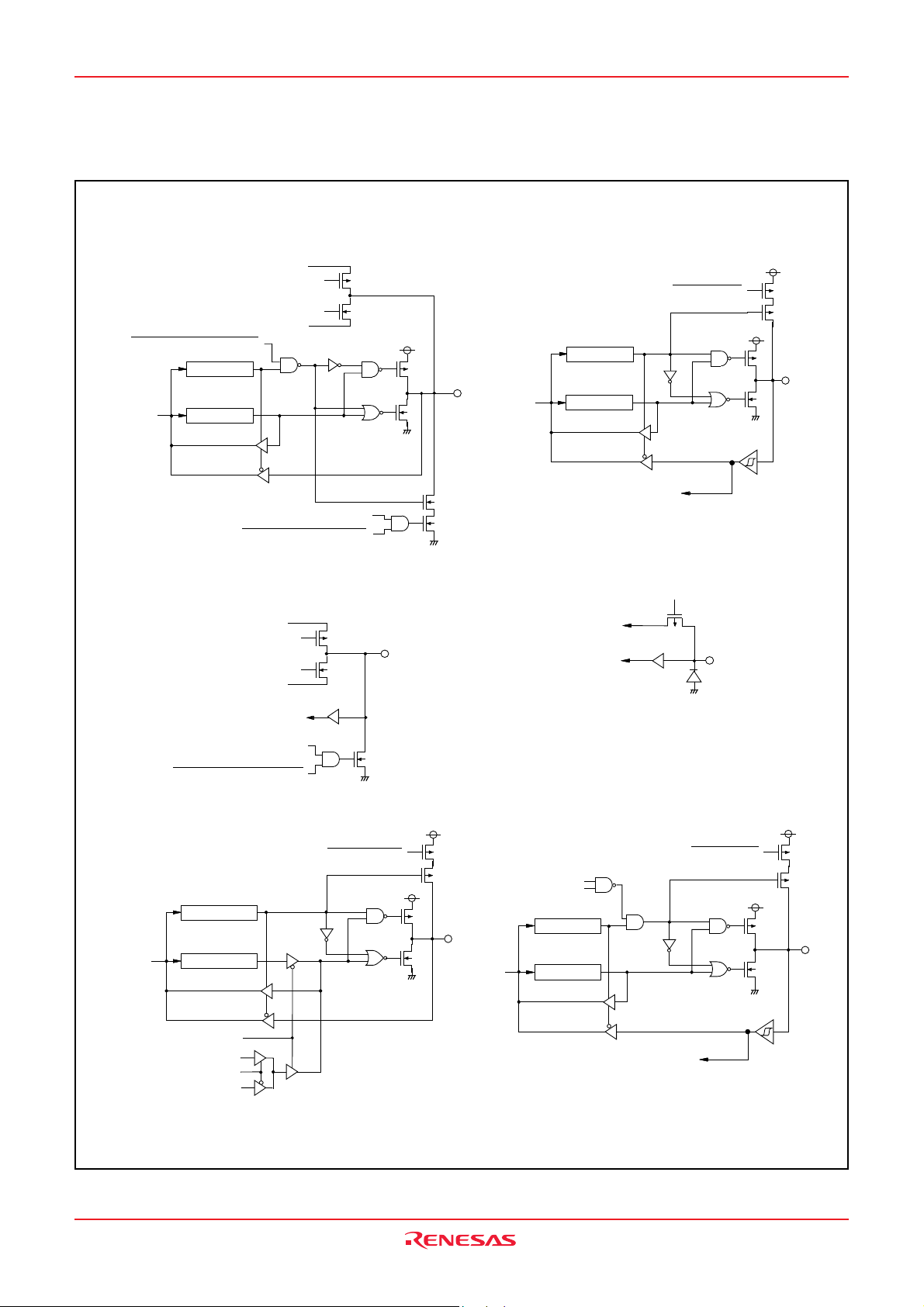
I/O PORTS
Direction Registers (ports P2, P4
1-P47, and
P5-P7)
The 3823 group has 49 programmable I/O pins arranged in seven
I/O ports (ports P0–P2, P41–P47 and P5-P7). The I/O ports P2,
P41–P47 and P5-P7 have direction registers which determine the
input/output direction of each individual pin. Each bit in a direction
register corresponds to one pin, and each pin can be set to be input port or output port.
When “0” is written to the bit corresponding to a pin, that pin becomes an input pin. When “1” is written to that bit, that pin becomes an output pin.
If data is read from a pin set to output, the value of the port output
latch is read, not the value of the pin itself. Pins set to input are
floating. If a pin set to input is written to, only the port output latch
is written to and the pin remains floating.
Direction Registers (ports P0 and P1)
Ports P0 and P1 have direction registers which determine the input/output direction of each individual port.
Each port in a direction register corresponds to one port, each port
can be set to be input or output. When “0” is written to the bit 0 of
a direction register, that port becomes an input port. When “1” is
written to that port, that port becomes an output port. Bits 1 to 7 of
ports P0 and P1 direction registers are not used.
0
register
(PULLA: address 001616)
00–P07 pull-down
P1
0
–P17 pull-down
P2
0
–P27 pull-up
P3
4
–P37 pull-down
P7
0
, P71 pull-up
Not used (return “0” when read)
0
register
(PULLB : address 001716)
41–P43 pull-up
P4
4
–P47 pull-up
P5
0
–P53 pull-up
P5
4
–P57 pull-up
P6
0
–P63 pull-up
P6
4
–P67 pull-up
Not used (return “0” when read)
ote: The contents of
do not affect ports programmed as the output port.
register A and
s a b l
0 :
1 : E n a b l e
e
register B
Fig. 12 Structure of PULL register A and PULL register B
Ports P3 and P40
These ports are only for input.
Pull-up/Pull-down Control
By setting the PULL register A (address 001616) or the PULL register B (address 001716), ports except for port P40 can control
either pull-down or pull-up (pins that are shared with the segment
output pins for LCD are pull-down; all other pins are pull-up) with
a program.
However, the contents of PULL register A and PULL register B do
not affect ports programmed as the output ports.
Rev.2.02 Jun 19, 2007 page 16 of 73
REJ03B0146-0202
Page 17

3823 Group
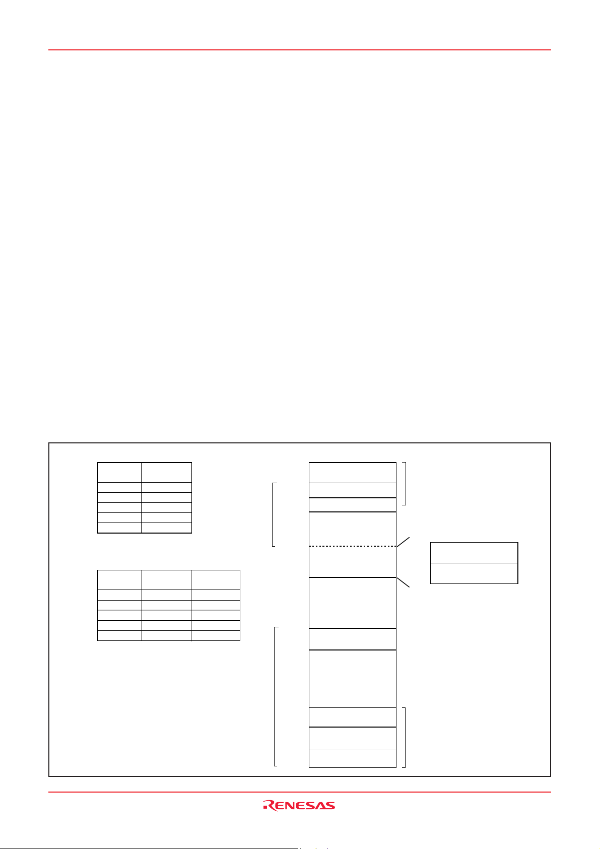
Table 7 List of I/O port function
Pin
P00/SEG16–
P07/SEG23
P10/SEG24–
P17/SEG31
Name
Port P0
Port P1
Input/Output
Input/output,
individual ports
I/O Format
CMOS compatible
input level
CMOS 3-state output
Non-Port Function
LCD segment output
Related SFRs
PULL register A
Segment output enable
register
Diagram No.
(1)
P20/KW0–
P27/KW7
P34/SEG12–
P37/SEG15
P40
P41/φ
P42/INT0,
Port P2
Port P3
Port P4
Input/output,
individual bits
Input
Input
Input/output,
individual bits
CMOS compatible
input level
CMOS 3-state output
CMOS compatible
input level
CMOS compatible
input level
CMOS compatible
input level
CMOS 3-state output
Key input (key-on
wake-up) interrupt
input
LCD segment output
QzROM program
power pin
φ clock output
XCIN frequency signal
output
External interrupt input
P43/INT1
P44/RXD
P45/TXD
Serial I/O function
input/output
P46/SCLK
P47/S
RDY/SOUT
P50/INT2,
P51/INT3
Port P5
Input/output,
individual bits
CMOS compatible
input level
External interrupt input
CMOS 3-state output
P52/RTP0,
P53/RTP1
P54/CNTR0
P55/CNTR1
P56/TOUT
P57/ADT
P60/AN0–
P67/AN7
Port P6
Input/output,
individual bits
CMOS compatible
input level
Real time port
function output
Timer X function I/O
Timer Y function input
Timer 2 function output
A/D trigger input
A/D conversion input
CMOS 3-state output
P70/XCOUT
P71/XCIN
COM0–COM3
SEG0–SEG11
Notes 1: For details of how to use double function ports as function I/O ports, refer to the applicable sections.
2: When an input level is at an intermediate potential, a current will flow from V
Especially, power source current may increase during execution of the STP and WIT instructions.
Fix the unused input pins to “H” or “L” through a resistor.
Port P7
Common
Segment
Input/output,
individual bits
Output
Output
CMOS compatible
input level
CMOS 3-state output
LCD common output
LCD segment output
Sub-clock
generating circuit I/O
CC to VSS through the input-stage gate.
PULL register A
Interrupt control register 2
PULL register A
Segment output enable
register
PULL register B
φ
output control register
Peripheral function
extension register
PULL register B
Interrupt edge selection
register
PULL register B
Serial I/O control register
Serial I/O status register
UART control register
Peripheral function
extension register
PULL register B
Interrupt edge selection
register
PULL register B
Timer X mode register
PULL register B
Timer X mode register
PULL register B
Timer Y mode register
PULL register B
Timer 123 mode register
PULL register B
A/D control register
PULL register A
CPU mode register
LCD mode register
(2)
(3)
(4)
(5)
(2)
(6)
(7)
(8)
(9)
(2)
(10)
(11)
(12)
(13)
(12)
(14)
(15)
(16)
(17)
(18)
Rev.2.02 Jun 19, 2007 page 17 of 73
REJ03B0146-0202
Page 18
3823 Group
(
)
t
(1) Ports P0, P1
S e g m e n t o u t p u t e n a b l e b i t
D a t a b u s
N o t e : B i t 0 o f d i r e c t i o n r e g i s t e r .
( 3 ) P o r t s P 34– P 3
N o t e
D i r e c t i o n r e g i s t e r
P o r t l a t c h
7
V
L 2
/ V
L 3
V
L 1
/ V
S S
P u l l - d o w n c o n t r o l
Segment output enable bit
V
L 2
/ V
L 3
VL1/V
SS
( 2 ) P o r t s P 2 , P 42, P 43, P 50, P 5
D i r e c t i o n r e g i s t e r
Data bus Port latch
Key input (Key-on wake-up) interrupt input
( 4 ) P o r t P 4
QZROM programmable
power source
INT
0
–INT3 interrupt input
0
Data bus
1
Pull-up control
S e g m e n t o u t p u t e n a b l e b i
(5) Port P4
1
D a t a b u s
φ o u t p u t c o n t r o l b i t
X
CIN
frequency signal
O u t p u t c l o c k s e l e c t i o n b i t
Pull-down control
D i r e c t i o n r e g i s t e r
Port latch
φ
D a t a b u s
Pull-up control
( 6 ) P o r t P 4
4
Serial I/O enable bit
R e c e i v e e n a b l e b i t
Direction register
Data bus Port latch
Pull-up control
Serial I/O input
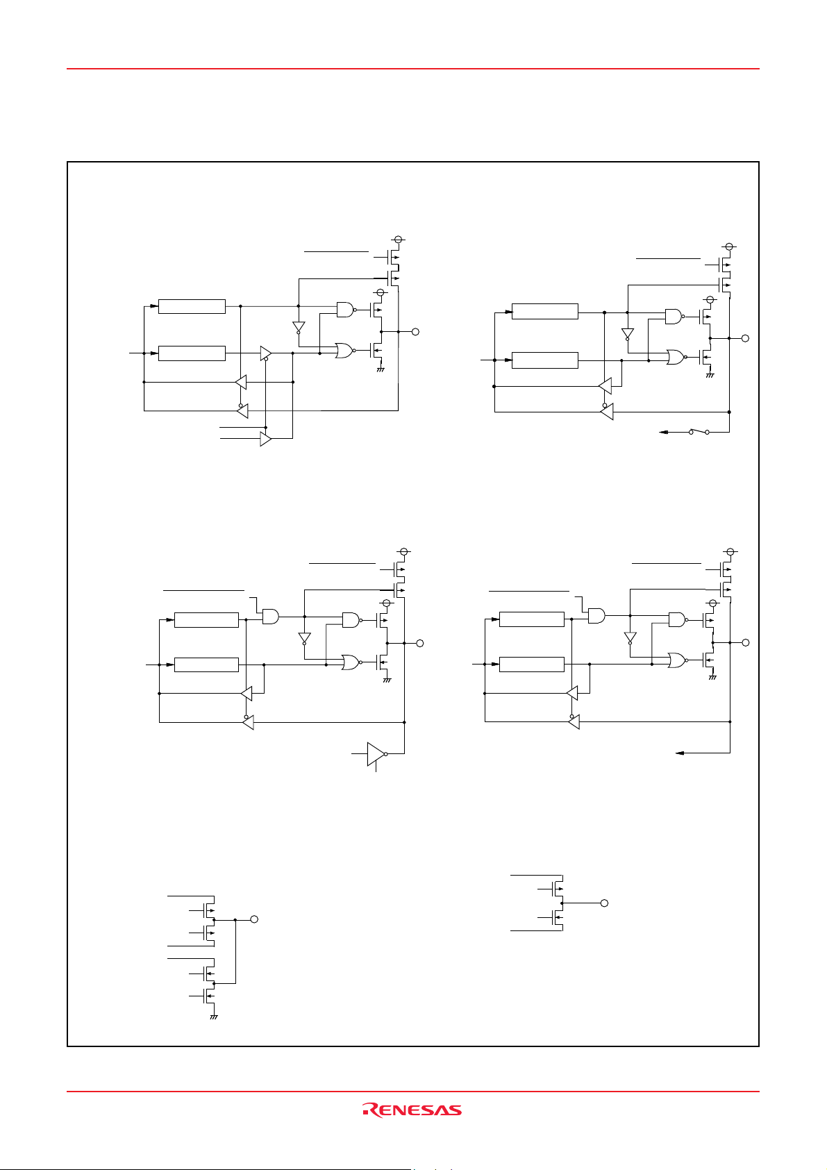
Fig. 13 Port block diagram (1)
Rev.2.02 Jun 19, 2007 page 18 of 73
REJ03B0146-0202
Page 19
3823 Group
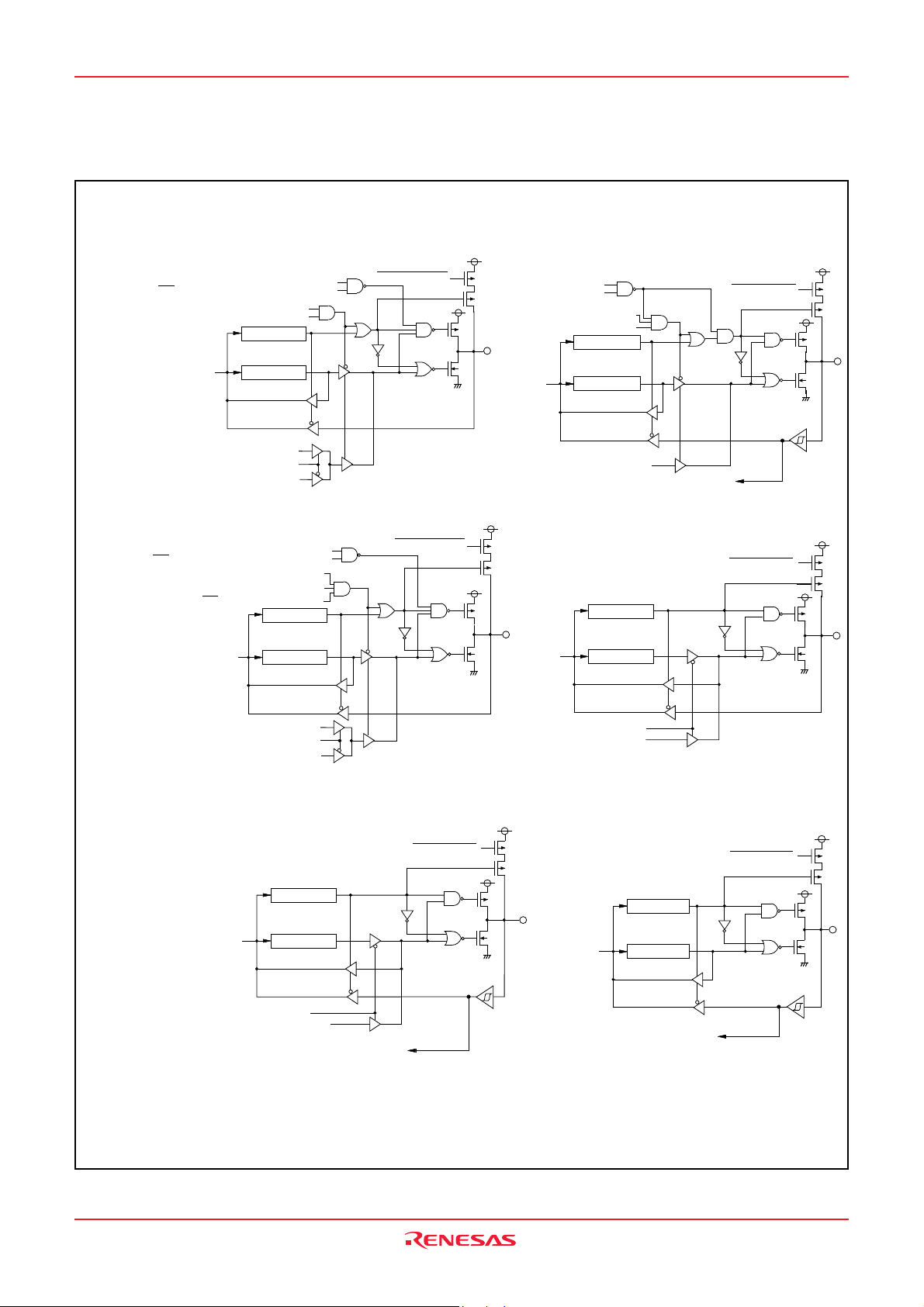
S
(
)
( 7 ) P o r t P 4
5
P-Channel output disabled selection bit
P 45/ T x D , P 47/ S
R D Y
/ S
O U T
P - c h a n n e l o u t p u t d i s a b l e b i t
Serial I/O enable bit
Transmit enable bit
D i r e c t i o n r e g i s t e r
D a t a b u s
P o r t l a t c h
As y n c h r o n o u s s e r i a l I / O o u t p u t
Sy n c h r o n o u s s e r i a l I / O o u t p u t p i n s e l e c t i o n b i t
e r i a l I / O o u t p u
s y n c h r o n o u s o r a s y n c h r o n o u s
(9) Port P4
7
P-Channel output disabled selection bit
P 45/ T x D , P 47/ S
R D Y
/ S
O U T
P - c h a n n e l o u t p u t d i s a b l e b i t
Serial I/O mode selection bit
Serial I/O enable bit
S
RDY,SOUT
output enable bit
D i r e c t i o n r e g i s t e r
D a t a b u s
Port latch
P u l l - u p c o n t r o l
( 8 ) P o r t P 4
synchronized selection bit
Serial I/O enable bit
Serial I/O mode selection bit
D a t a b u s
6
Serial I/O clock-
P u l l - u p c o n t r o l
Serial I/O enable bit
Direction register
Port latch
S e r i a l I / O c l o c k o u t p u t
t
(10) Ports P5
2, P53
S e r i a l I / O c l o c k i n p u t
Pull-up control
Pull-up control
Direction register
Port latchData bus
Synchronous serial I/O output
Synchronous serial I/O output pin s election bit
S e r i a l I / O r e a d y o u t p u t
( 1 1 ) P o r t P 5
4
D i r e c t i o n r e g i s t e r
P o r t l a t c hD a t a b u s
T i m e r X o p e r a t i n g m o d e b i t
(Pulse output mode selection)
T i m e r o u t p u t
CNTR
0
interrupt input
Pull-up control
R e a l t i m e p o r t c o n t r o l b i t
D a t a f o r r e a l t i m e p o r t
( 1 2 ) P o r t s P 5
D a t a b u s
5 ,
P 5
7
Direction register
Port latch
CNTR
1
A/D trigger interrupt input
interrupt input
Pull-up control
Fig. 14 Port block diagram (2)
Rev.2.02 Jun 19, 2007 page 19 of 73
REJ03B0146-0202
Page 20
3823 Group
( 1 3 ) P o r t P 56
D a t a b u s
U
o u t p u t c o n t r o l b i
TO
T
( 1 5 ) P o r t P 70
D i r e c t i o n r e g i s t e r
P o r t l a t c h
T i m e r o u t p u t
s w i t c h b i
P o r t X
C
D i r e c t i o n r e g i s t e r
t
s w i t c h b i t + P u l l - u p c o n t r o
P o r t X
( 1 4 ) P o r t P 6
P u l - u p c o n t r o l
Data bus
Direction register
Port latch
A / D c o n v e r s i o n i n p u t
P u l l - u p c o n t r o l
A n a l o g i n p u t p i n s e l e c t i o n b i t
( 1 6 ) P o r t P 71
s w i t c h b i t + P u l l - u p c o n t r o
C
t
l
Port X
P o r t X
C switch bit
Direction register
C
l
D a t a b u s
P o r t l a t c h
( 1 7 ) C O M0– C O M3
L 3
V
VL
2
VL
1
Fig. 15 Port block diagram (3)
O s c i l l a t i o n c i r c u i t
P o r t P 71
P o r t XC s w i t c h b i t
T h e g a t e i n p u t s i g n a l o f e a c h t r a n s i s t o r i s
c o n t r o l l e d b y t h e L C D d u t y r a t i o a n d t h e
b i a s v a l u e .
D a t a b u s
( 1 8 ) S E G0– S E G1
VL
2/
VL
3
VL
1/
VS
S
Port latch
S u b - c l o c k g e n e r a t i n g c i r c u i t i n p u t
1
T h e v o l t a g e a p p l i e d t o t h e s o u r c e s o f
P - c h a n n e l a n d N - c h a n n e l t r a n s i s t o r s
i s t h e c o n t r o l l e d v o l t a g e b y t h e b i a s
v a l u e .
Rev.2.02 Jun 19, 2007 page 20 of 73
REJ03B0146-0202
Page 21

3823 Group
Termination of unused pins
• Termination of common pins
I/O ports: Select an input port or an output port and follow
each processing method.
Output ports: Open.
Input ports: If the input level become unstable, through current
flow to an input circuit, and the power supply current
may increase.
Especially, when expecting low consumption current
(at STP or WIT instruction execution etc.), pull-up or
pull-down input ports to prevent through current
(built-in resistor can be used). Pull-down the P40/
(VPP) pin.
We recommend processing unused pins through a
resistor which can secure IOH(avg) or IOL(avg).
Because, when an I/O port or a pin which have an
output function is selected as an input port, it may
operate as an output port by incorrect operation etc.
Rev.2.02 Jun 19, 2007 page 21 of 73
REJ03B0146-0202
Page 22
3823 Group
Table 8 Termination of unused pins
Pin
P00/SEG16–P17/SEG23
P10/SEG24–P17/SEG31
P20/KW0–P27/KW7
P34/SEG12–P37/SEG15
P40/(VPP)
P41/φ
P42/INT0
P43/INT1
P44/RxD
P45/TxD
P46/SCLK
P47/SRDY/SOUT
P50/INT2
P51/INT3
P52/RTP0
P53/RTP1
P54/CNTR0
P55/CNTR1
P56/TOUT
P57/ADT
P60/AN0–P67/AN7
P70/XCOUT
P71/XCIN
VL3 (Note)
VL2 (Note)
VL1 (Note)
COM0–COM3
SEG0–SEG
AVSS
VREF
XOUT
Note : The termination of VL3, VL2 and VL1 is applied when the bit 3 of the LCD mode register is “0”
11
Termination 1 (recommend)
I/O port
Input port
Input port (pull-down)
I/O port
Connect to VSS
Connect to VSS
Connect to VSS
Open
Open
Connect to VSS
Connect to VCC or VSS
When an external clock is
input to the XIN pin, leave
the XOUT pin open.
When selecting SEG output, open.
When selecting KW function, perform
termination of input port.
When selecting SEG output, open.
When selecting φ output, open.
When selecting INT0 function,
perform termination of input port.
When selecting INT1 function,
perform termination of input port.
When selecting RXD function,
perform termination of input port.
When selecting TXD function,
perform termination of output port.
When selecting external clock input,
perform termination of input port.
When selecting SRDY function,
perform termination of output port.
When selecting INT2 function,
perform termination of input port.
When selecting INT3 function,
perform termination of input port.
When selecting RTP0 function,
perform termination of output port.
When selecting RTP1 function,
perform termination of output port.
When selecting CNTR0 input function,
perform termination of input port.
When selecting CNTR1 function,
perform termination of input port.
When selecting TOUT function,
perform termination of output port.
When selecting ADT function,
perform termination of input port.
When selecting AN function, these
pins can be opened. (A/D conversion
result cannot be guaranteed.)
Do not select XCIN-XCOUT oscillation
function by program.
Termination 2
–
–
–
–
–
–
–
–
–
Termination 3
–
–
–
–
–
–
–
–
–
When selecting internal clock output,
perform termination of output port.
When selecting SOUT function,
perform termination of output port.
–
–
–
–
When selecting CNTR0 output function,
perform termination of output port.
–
–
–
–
–
–
–
–
–
–
–
–
–
Rev.2.02 Jun 19, 2007 page 22 of 73
REJ03B0146-0202
Page 23

3823 Group
INTERRUPTS
The 3823 group interrupts are vector interrupts with a fixed priority scheme, and generated by 16 sources among 17 sources: 8
external, 8 internal, and 1 software.
The interrupt sources, vector addresses
are shown in Table 9.
Each interrupt except the BRK instruction interrupt has the interrupt request bit and the interrupt enable bit. These bits and the
interrupt disable flag (I flag) control the acceptance of interrupt requests. Figure 16 shows an interrupt control diagram.
Table 9 Interrupt vector addresses and priority
Interrupt Source
Reset (Note 2)
INT0
INT1
Serial I/O
reception
Serial I/O
transmission
Timer X
Timer Y
Timer 2
Timer 3
CNTR0
CNTR1
Timer 1
INT2
INT3
Key input
(Key-on wake-up)
ADT
A/D conversion
BRK instruction
Notes1: Vector addresses contain interrupt jump destination addresses.
2: Reset function in the same way as an interrupt with the highest priority.
Priority
1
2
3
4
5
6
7
8
9
10
11
12
13
14
15
16
17
(1)
, and interrupt priority
Vector Addresses (Note 1)
LowHigh
FFFD16
FFFB16
FFF916
FFF716
FFF516
FFF316
FFF116
FFEF16
FFED16
FFEB16
FFE916
FFE716
FFE516
FFE316
FFE116
FFDF16
FFDD16
FFFC16
FFFA16
FFF816
FFF616
FFF416
FFF216
FFF016
FFEE16
FFEC16
FFEA16
FFE816
FFE616
FFE416
FFE216
FFE016
FFDE16
FFDC16
An interrupt requests is accepted when all of the following
conditions are satisfied:
• Interrupt disable flag.................................“0”
• Interrupt disable request bit .....................“1”
• Interrupt enable bit................................... “1”
Though the interrupt priority is determined by hardware, priority
processing can be performed by software using the above bits
and flag.
Interrupt Request
Generating Conditions
At reset
At detection of either rising or
falling edge of INT0 input
At detection of either rising or
falling edge of INT1 input
At completion of serial interface
data reception
At completion of serial interface
transmit shift or when transmission buffer is empty
At timer X underflow
At timer Y underflow
At timer 2 underflow
At timer 3 underflow
At detection of either rising or
falling edge of CNTR0 input
At detection of either rising or
falling edge of CNTR1 input
At timer 1 underflow
At detection of either rising or
falling edge of INT2 input
At detection of either rising or
falling edge of INT3 input
At falling of conjunction of input
level for port P2 (at input mode)
At falling of ADT input
At completion of A/D conversion
At BRK instruction execution
Non-maskable
External interrupt
(active edge selectable)
External interrupt
(active edge selectable)
Valid when serial interface is se-
lected
Valid when serial interface is se-
lected
External interrupt
(active edge selectable)
External interrupt
(active edge selectable)
External interrupt
(active edge selectable)
External interrupt
(active edge selectable)
External interrupt
(Valid at falling)
Valid when ADT interrupt is selected, External interrupt
(Valid at falling)
Valid when A/D interrupt is selected
Non-maskable software interrupt
Remarks
Rev.2.02 Jun 19, 2007 page 23 of 73
REJ03B0146-0202
Page 24

3823 Group
t
t
t
I n t e r r u p t r e q u e s t b i
I n t e r r u p t e n a b l e b i
I n t e r r u p t d i s a b l e f l a g ( I )
Fig. 16 Interrupt control diagram
B R K i n s t r u c t i o n
R e s e
i n t e r r u p t r e q u e s t
Interrupt Disable Flag
The interrupt disable flag is assigned to bit 2 of the processor status register. This flag controls the acceptance of all interrupt
requests except for the BRK instruction. When this flag is set to
“1”, the acceptance of interrupt requests is disabled. When it is set
to “0”, acceptance of interrupt requests is enabled. This flag is set
to “1” with the SET instruction and set to “0” with the CLI instruction.
When an interrupt request is accepted, the contents of the processor status register are pushed onto the stack while the interrupt
disable flag remaines set to “0”. Subsequently, this flag is automatically set to “1” and multiple interrupts are disabled.
To use multiple interrupts, set this flag to “0” with the CLI instruction within the interrupt processing routine.
The contents of the processor status register are popped off the
stack with the RTI instruction.
Interrupt Request Bits
Once an interrupt request is generated, the corresponding interrupt request bit is set to “1” and remaines “1” until the request is
accepted. When the request is accepted, this bit is automatically
set to “0”.
Each interrupt request bit can be set to “0”, but cannot be set to
“1”, by software.
Interrupt Enable Bits
The interrupt enable bits control the acceptance of the corresponding interrupt requests. When an interrupt enable bit is set to
“0”, the acceptance of the corresponding interrupt request is disabled. If an interrupt request occurs in this condition, the
corresponding interrupt request bit is set to “1”, but the interrupt
request is not accepted. When an interrupt enable bit is set to “1”,
acceptance of the corresponding interrupt request is enabled.
Each interrupt enable bit can be set to “0” or “1” by software.
The interrupt enable bit for an unused interrupt should be set to
“0”.
Interrupt Source Selection
The following combinations can be selected by the interrupt
source selection bit of the AD control register (bit 6 of the address
003916).
• ADT or A/D conversion (refer Table 9)
Rev.2.02 Jun 19, 2007 page 24 of 73
REJ03B0146-0202
Page 25

3823 Group
b
b
I
I N T
i
( I N T E D G E
A
)
I
I N T
i
I
I N T
i
N
d
( I R E Q
C
)
( I C O N
E
)
I
C N T R
i
(IREQ
D16)
I
CNTR
d
(ICON
F16)
F
b7b
b7b
b
b
b7b
7
n t e r r u p t e d g e s e l e c t i o n r e g i s t e
0
: a d d r e s s 0 0 3
n t e r r u p t e d g e s e l e c t i o n b i
0
I N T
1
i n t e r r u p t e d g e s e l e c t i o n b i t
I N T
2
i n t e r r u p t e d g e s e l e c t i o n b i t
3
i n t e r r u p t e d g e s e l e c t i o n b i t
I N T
N o t u s e d ( r e t u r n “ 0 ” w h e n r e a d )
0
n t e r r u p t r e q u e s t r e g i s t e r
1 : a d d r e s s 0 0 3
n t e r r u p t r e q u e s t b i
0
1
i n t e r r u p t r e q u e s t b i t
I N T
S e r i a l I / O r e c e i v e i n t e r r u p t r e q u e s t b i t
S e r i a l I / O t r a n s m i t i n t e r r u p t r e q u e s t b i t
T i m e r X i n t e r r u p t r e q u e s t b i t
T i m e r Y i n t e r r u p t r e q u e s t b i t
T i m e r 2 i n t e r r u p t r e q u e s t b i t
T i m e r 3 i n t e r r u p t r e q u e s t b i t
r
1 6
t
a l l i n g e d g e a c t i v
0 :
e
1 : R i s i n g e d g e a c t i v e
1
1 6
7
t
0
n t e r r u p t r e q u e s t r e g i s t e r
2 : address 003
n t e r r u p t r e q u e s t b i
0
1
i n t e r r u p t r e q u e s t b i t
C N T R
2
t
T i m e r 1 i n t e r r u p t r e q u e s t b i t
I N T
2
i n t e r r u p t r e q u e s t b i t
3
i n t e r r u p t r e q u e s t b i t
I N T
K e y i n p u t i n t e r r u p t r e q u e s t b i t
A D T / A D c o n v e r s i o n i n t e r r u p t r e q u e s t b i t
N o t u s e d ( r e t u r n s “ 0 ” w h e n r e a d )
o i n t e r r u p t r e q u e s t i s s u e
0 :
1 : I n t e r r u p t r e q u e s t i s s u e d
0
nterrupt control register 1
1 : a d d r e s s 0 0 3
n t e r r u p t e n a b l e b i
I N T
0
1
i n t e r r u p t e n a b l e b i t
1 6
S e r i a l I / O r e c e i v e i n t e r r u p t e n a b l e b i t
S e r i a l I / O t r a n s m i t i n t e r r u p t e n a b l e b i t
T i m e r X i n t e r r u p t e n a b l e b i t
T i m e r Y i n t e r r u p t e n a b l e b i t
T i m e r 2 i n t e r r u p t e n a b l e b i t
T i m e r 3 i n t e r r u p t e n a b l e b i t
t
0
nterrupt control register 2
2 : address 003
0
interrupt enable bit
CNTR
1
interrupt enable bit
Timer 1 interrupt enable bit
INT
2
interrupt enable bit
3
interrupt enable bit
INT
Key input interrupt enable bit
ADT/AD conversion interrupt enable bit
Not used (returns “0” when read)
(Do not write “1” to this bit.)
0 : Interrupts disable
1 : Interrupts enabled
Fig. 17 Structure of interrupt-related registers
Rev.2.02 Jun 19, 2007 page 25 of 73
REJ03B0146-0202
Page 26

3823 Group
Interrupt Request Generation, Acceptance,
and Handling
Interrupts have the following three phases.
(i) Interrupt Request Generation
An interrupt request is generated by an interrupt source (external interrupt signal input, timer underflow, etc.) and the
corresponding request bit is set to “1”.
(ii) Interrupt Request Acceptance
Based on the interrupt acceptance timing in each instruction
cycle, the interrupt control circuit determines acceptance conditions (interrupt request bit, interrupt enable bit, and interrupt
disable flag) and interrupt priority levels for accepting interrupt
requests. When two or more interrupt requests are generated
simultaneously, the highest priority interrupt is accepted. The
value of interrupt request bit for an unaccepted interrupt remains the same and acceptance is determined at the next
interrupt acceptance timing point.
(iii) Handling of Accepted Interrupt Request
The accepted interrupt request is processed.
Figure 18 shows the time up to execution in the interrupt processing routine, and Figure 19 shows the interrupt sequence.
Figure 20 shows the timing of interrupt request generation, interrupt request bit, and interrupt request acceptance.
Interrupt Handling Execution
When interrupt handling is executed, the following operations are
performed automatically.
(1) Once the currently executing instruction is completed, an inter-
rupt request is accepted.
(2) The contents of the program counters and the processor status
register at this point are pushed onto the stack area in order
from 1 to 3.
1. High-order bits of program counter (PCH)
2. Low-order bits of program counter (PCL)
3. Processor status register (PS)
(3) Concurrently with the push operation, the jump address of the
corresponding interrupt (the start address of the interrupt processing routine) is transferred from the interrupt vector to the
program counter.
(4) The interrupt request bit for the corresponding interrupt is set
to “0”. Also, the interrupt disable flag is set to “1” and multiple
interrupts are disabled.
(5) The interrupt routine is executed.
(6) When the RTI instruction is executed, the contents of the reg-
isters pushed onto the stack area are popped off in the order
from 3 to 1. Then, the routine that was before running interrupt
processing resumes.
As described above, it is necessary to set the stack pointer and
the jump address in the vector area corresponding to each interrupt to execute the interrupt processing routine.
■Notes
The interrupt request bit may be set to “1” in the following cases.
•When setting the external interrupt active edge
Related registers: Interrupt edge selection register
(address 003A16)
Timer X mode register (address 002716)
Timer Y mode register (address 002816)
If it is not necessary to generate an interrupt synchronized with
these settings, take the following sequence.
(1) Set the corresponding enable bit to “0” (disabled).
(2) Set the interrupt edge selection bit (the active edge switch
bit) or the interrupt source bit.
(3) Set the corresponding interrupt request bit to “0” after one or
more instructions have been executed.
(4) Set the corresponding interrupt enable bit to “1” (enabled).
Interrupt request
generated
Main routine
*
When executing DIV instruction
*
0 to 16 cycles
Interrupt request
acceptance
7 to 23 cycles
Interrupt sequence
Stack push and
Vector fetch
7 cycles
Interrupt routine
starts
Interrupt handling
routine
Fig. 18 Time up to execution in interrupt routine
Push onto stack
Vector fetch
φ
SYNC
RD
WR
Address bus
Data busPCNot used
SYNC :CPU operation code fetch cycle
(This is an internal signal that cannot be observed from the external unit.)
BL, BH:Vector address of each interrupt
AL, AH:Jump destination address of each interrupt
SPS :“00
16
” or “0116”
([SPS] is a page selected by the stack page selection bit of CPU mode register.)
S,SPS S-1,SPS S-2,SPS
PCHPCLPS ALA
BLBHAL,A
Execute interrupt
routine
H
H
Fig. 19 Interrupt sequence
Rev.2.02 Jun 19, 2007 page 26 of 73
REJ03B0146-0202
Page 27

3823 Group
Instruction cycle
Internal clock φ
SYNC
21
T1 IR1 T2
T1 T2 T3: Interrupt acceptance timing points
IR1 IR2: Timings points at which the interrupt request bit is set to “1”.
Note: Period 2 indicates the last φ cycle during one instruction cycle.
(1) The interrupt request bit for an interrupt request generated during period 1 is set to “1” at timing point IR1.
(2) The interrupt request bit for an interrupt request generated during period 2 is set to “1” at timing point IR1 or IR2.
The timing point at which the bit is set to “1” varies depending on conditions. When two or more interrupt requests
are generated during the period 2, each request bit may be set to “1” at timing point IR1 or IR2 separately.
Push onto stack
Vector fetch
Fig. 20 Timing of interrupt request generation, interrupt request bit, and interrupt acceptance
Instruction cycle
IR2 T3
Rev.2.02 Jun 19, 2007 page 27 of 73
REJ03B0146-0202
Page 28

3823 Group
Key Input Interrupt (Key-on wake-up)
A Key-on wake-up interrupt request is generated by applying a
falling edge to any pin of port P2 that have been set to input mode.
In other words, it is gener1ated when AND of input level goes from
Port PX
X
“L” level output
P U L L r e g i s t e r A b i t 2 = “ 1 ”
P 2
P 2
P2
7
o u t p u t
6
o u t p u t
5
output
✽
✽
✽
✽✽
Port P2
7
latch
✽✽
✽✽
Port P2
latch
Port P2
latch
6
5
“1” to “0”. An example of using a key input interrupt is shown in
Figure 21, where an interrupt request is generated by pressing
one of the keys consisted as an active-low key matrix which inputs
to ports P20–P23.
Port P2
7
direction register = “1”
P o r t P 2
6
d i r e c t i o n r e g i s t e r = “ 1 ”
Port P2
5
direction register = “1”
Key input interrupt request
P2
4
P 2
P2
P 2
P2
output
3
i n p u t
2
input
1
i n p u t
0
input
Port P2
4
✽
✽
✽
✽
✽
✽✽
Port P2
latch
✽✽
Port P2
latch
✽✽
Port P2
latch
✽✽
Port P2
latch
✽
Port P2
latch
direction register = “1”
4
P o r t P 2
3
d i r e c t i o n r e g i s t e r = “ 0 ”
3
2
Port P2
direction register = “0”
2
Port P2
1
direction register = “0”
1
Port P2
0
direction register = “0”
0
P o r t P 2
I n p u t r e a d i n g c i r c u i t
✽ P-channel transistor for pull-up
✽✽ CMOS output buffer
Fig. 21 Connection example when using key input interrupt and port P2 block diagram
Rev.2.02 Jun 19, 2007 page 28 of 73
REJ03B0146-0202
Page 29

3823 Group
TIMERS
The 3823 group has five timers: timer X, timer Y, timer 1, timer 2,
and timer 3. Timer X and timer Y are 16-bit timers, and timer 1,
timer 2, and timer 3 are 8-bit timers.
All timers are down count timers. When the timer reaches “0016”,
an underflow occurs at the next count pulse and the corresponding timer latch is reloaded into the timer and the count is
continued. When a timer underflows, the interrupt request bit cor-
Real time port
control bit “1”
P5
2
P52 direction register
P5
3
P5
3
direction register
4
/CNTR
P5
0
f(XIN)/16
(f(SUB)/16 in low-speed mode✽)
CNTR
edge switch bit
Pulse width
measurement
mode
P5
Real time port
control bit “1”
P5
0
active
“0”
“1”
CNTR0 active
edge switch bit
P54 direction register
Pulse output mode
CNTR1 active
edge switch bit
P55/CNTR
1
“0”
“1”
f(XIN)/16
(f(SUB)/16 in low-speed mode])
Timer 1 count source
selection bit
f(SUB)
T
OUT
output
control bit
P5
6/TOUT
6
direction register
P5
f(XIN)/16(f(SUB)/16 in low-speed mode✽)
✽
f(SUB) is the source oscillation frequency in low-speed mode.
f(SUB) shows the oscillation frequency of X
oscillator.
Internal clock φ is f(SUB)/2 in the low-speed mode.
CIN
Q D
Latch
“0”
2
latch
Q D
Latch
“0”
3
latch
Timer X operating mode bits
“00”,“01”,“11”
“10”
P5
4
latch
f(XIN)/16
SUB
(f(
“00”,“01”,“11”
“10”
“0”
“1”
OUT
T
active edge
switch bit
6
latch
P5
or the on-chip
P5
P5
Real time port
control bit “0”
Timer X stop
control bit
“0”
S
Q
“1”
)16 in low-speed mode✽)
Timer Y operating
mode bits
T
Q
Timer Y stop
control bit
Timer 1 latch (8)
Timer 1 (8)
output
OUT
output
T
control bit
“0”
“1”
S
Q
T
Q
responding to that timer is set to “1”.
Read and write operation on 16-bit timer must be performed for
both high and low-order bytes. When reading a 16-bit timer, read
the high-order byte first. When writing to a 16-bit timer, write the
low-order byte first. The 16-bit timer cannot perform the correct
operation when reading during the write operation, or when writing
during the read operation.
Data bus
2
data for real time port
3
data for real time port
“1”
Timer X (low) latch (8) Timer X (high) latch (8)
Rising edge detection
Falling edge detection
Timer Y (low) latch (8)
Timer Y (low) (8)
Timer 3 count
source selection bit
Timer X mode register
write signal
Timer X write
control bit
Timer X (low) (8)
Pulse output
mode
Timer X (high) (8)
Timer Y operating mode bits
Pulse width HL continuously measurement mode
Period
measurement mode
Timer Y (high) latch (8)
Timer Y (high) (8)
Timer 2 count source
selection bit
“0”
Timer 2 latch (8)
Timer 2 (8)
“1”
f(XIN)/16
(f(SUB)/16 in low-speed mode
Timer 3 latch (8)
“0”
✽
)
Timer 3 (8)
“1”
“00”,“01”,“10”
“11”
Timer 2 write
control bit
Timer X
interrupt
request
CNTR
interrupt
request
CNTR
interrupt
request
Timer Y
interrupt
request
Timer 1
interrupt
request
Timer 2
interrupt
request
Timer 3
interrupt
request
0
1
Fig. 22 Timer block diagram
Rev.2.02 Jun 19, 2007 page 29 of 73
REJ03B0146-0202
Page 30

3823 Group
T i
T i
b
b
Timer X
Timer X is a 16-bit timer that can be selected in one of four modes
and can be controlled the timer X write and the real time port by
setting the timer X mode register.
●Real time port control
While the real time port function is valid, data for the real time port
are output from ports P52 and P53 each time the timer X
underflows. (However, after rewriting a data for real time port, if
the real time port control bit is changed from “0” to “1”, data are
(1) Timer Mode
The timer counts f(XIN)/16 (or f(SUB)/16 in low-speed mode).
f(SUB) is the source oscillation frequency in low-speed mode.
f(SUB) shows the oscillation frequency of XCIN or the on-chip oscillator. Internal clock φ is f(XCIN)/2 in the low-speed mode.
(2) Pulse Output Mode
Each time the timer underflows, a signal output from the CNTR0
pin is inverted. Except for this, the operation in pulse output mode
is the same as in timer mode. When using a timer in this mode,
output independent of the timer X operation.) If the data for the
real time port is changed while the real time port function is valid,
the changed data are output at the next underflow of timer X.
Before using this function, set the corresponding port direction
registers to output mode.
■Note on CNTR0 interrupt active edge
selection
CNTR0 interrupt active edge depends on the CNTR0 active edge
switch bit.
set the corresponding port P54 direction register to output mode.
(3) Event Counter Mode
The timer counts signals input through the CNTR0 pin.
7
Except for this, the operation in event counter mode is the same
as in timer mode. When using a timer in this mode, set the corresponding port P54 direction register to input mode.
(4) Pulse Width Measurement Mode
The count source is f(XIN)/16 (or f(SUB)/16 in low-speed mode). If
CNTR0 active edge switch bit is “0”, the timer counts while the in-
put signal of CNTR0 pin is at “H”. If it is “1”, the timer counts while
the input signal of CNTR0 pin is at “L”. When using a timer in this
mode, set the corresponding port P54 direction register to input
mode.
●Timer X write control
If the timer X write control bit is “0”, when the value is written in the
address of timer X, the value is loaded in the timer X and the latch
at the same time.
If the timer X write control bit is “1”, when the value is written in the
address of timer X, the value is loaded only in the latch. The value
in the latch is loaded in timer X after timer X underflows.
If the value is written in latch only, when writing in the timer latch at
the timer underflow, the value is set in the timer and the latch at
one time. Additionally, unexpected value may be set in the high-order counter when the writing in high-order latch and the underflow
of timer X are performed at the same timing.
Fig. 23 Structure of timer X mode register
0
m e r X m o d e r e g i s t e
( T X M : a d d r e s s 0 0 2 7
m e r X w r i t e c o n t r o l b i
0 : W r i t e v a l u e i n l a t c h a n d c o u n t e r
1 : W r i t e v a l u e i n l a t c h o n l y
R e a l t i m e p o r t c o n t r o l b i t
0 : R e a l t i m e p o r t f u n c t i o n i n v a l i d
1 : R e a l t i m e p o r t f u n c t i o n v a l i d
2
d a t a f o r r e a l t i m e p o r t
P 5
3
d a t a f o r r e a l t i m e p o r t
P 5
T i m e r X o p e r a t i n g m o d e b i t s
b 5 b 4
0 0 : T i m e r m o d e
0 1 : P u l s e o u t p u t m o d e
1 0 : E v e n t c o u n t e r m o d e
1 1 : P u l s e w i d t h m e a s u r e m e n t m o d e
0
a c t i v e e d g e s w i t c h b i t
C N T R
0 : C o u n t a t r i s i n g e d g e i n e v e n t c o u n t e r m o d e
S t a r t f r o m “ H ” o u t p u t i n p u l s e o u t p u t m o d e
M e a s u r e “ H ” p u l s e w i d t h i n p u l s e w i d t h
m e a s u r e m e n t m o d e
F a l l i n g e d g e a c t i v e f o r C N T R
1 : C o u n t a t f a l l i n g e d g e i n e v e n t c o u n t e r m o d e
S t a r t f r o m “ L ” o u t p u t i n p u l s e o u t p u t m o d e
M e a s u r e “ L ” p u l s e w i d t h i n p u l s e w i d t h
m e a s u r e m e n t m o d e
R i s i n g e d g e a c t i v e f o r C N T R
T i m e r X s t o p c o n t r o l b i t
0 : C o u n t s t a r t
1 : C o u n t s t o p
r
1 6
)
t
0
i n t e r r u p t
0
i n t e r r u p t
Rev.2.02 Jun 19, 2007 page 30 of 73
REJ03B0146-0202
Page 31

3823 Group
T i
b
b
N
)
Timer Y
Timer Y is a 16-bit timer that can be selected in one of four modes.
(1) Timer Mode
The timer counts f(XIN)/16 (or f(SUB)/16 in low-speed mode).
(2) Period Measurement Mode
CNTR1 interrupt request is generated at rising/falling edge of
CNTR1 pin input signal. Simultaneously, the value in timer Y latch
is reloaded in timer Y and timer Y continues counting down. Except for the above-mentioned, the operation in period
measurement mode is the same as in timer mode.
The timer value just before the reloading at rising/falling of CNTR1
pin input signal is retained until the timer Y is read once after the
reload.
The rising/falling timing of CNTR1 pin input signal is found by
CNTR1 interrupt. When using a timer in this mode, set the corresponding port P55 direction register to input mode.
7
0
m e r Y m o d e r e g i s t e
( T Y M : a d d r e s s 0 0 2 8
o t u s e d ( r e t u r n “ 0 ” w h e n r e a d
T i m e r Y o p e r a t i n g m o d e b i t s
b 5 b 4
0 0 : T i m e r m o d e
0 1 : P e r i o d m e a s u r e m e n t m o d e
1 0 : E v e n t c o u n t e r m o d e
1 1 : P u l s e w i d t h H L c o n t i n u o u s l y m e a s u r e m e n t
m o d e
1
a c t i v e e d g e s w i t c h b i t
C N T R
0 : C o u n t a t r i s i n g e d g e i n e v e n t c o u n t e r m o d e
M e a s u r e t h e f a l l i n g e d g e t o f a l l i n g e d g e
p e r i o d i n p e r i o d m e a s u r e m e n t m o d e
F a l l i n g e d g e a c t i v e f o r C N T R
1 : C o u n t a t f a l l i n g e d g e i n e v e n t c o u n t e r m o d e
M e a s u r e t h e r i s i n g e d g e p e r i o d i n p e r i o d
m e a s u r e m e n t m o d e
R i s i n g e d g e a c t i v e f o r C N T R
T i m e r Y s t o p c o n t r o l b i t
0 : C o u n t s t a r t
1 : C o u n t s t o p
r
1 6
)
1
i n t e r r u p t
1
i n t e r r u p t
(3) Event Counter Mode
The timer counts signals input through the CNTR1 pin.
Except for this, the operation in event counter mode is the same
as in timer mode. When using a timer in this mode, set the corresponding port P55 direction register to input mode.
(4) Pulse Width HL Continuously Measurement
Mode
CNTR1 interrupt request is generated at both rising and falling
edges of CNTR1 pin input signal. Except for this, the operation in
pulse width HL continuously measurement mode is the same as in
period measurement mode. When using a timer in this mode, set
the corresponding port P55 direction register to input mode.
■Note on CNTR1 interrupt active edge selection
CNTR1 interrupt active edge depends on the CNTR1 active edge
switch bit. However, in pulse width HL continuously measurement
mode, CNTR1 interrupt request is generated at both rising and
falling edges of CNTR1 pin input signal regardless of the setting of
CNTR1 active edge switch bit.
Fig. 24 Structure of timer Y mode register
Rev.2.02 Jun 19, 2007 page 31 of 73
REJ03B0146-0202
Page 32

3823 Group
T
i
T i
N
f ( S U B )
b7b
Timer 1, Timer 2, Timer 3
Timer 1, timer 2, and timer 3 are 8-bit timers. The count source for
each timer can be selected by timer 123 mode register. The timer
latch value is not affected by a change of the count source. However, because changing the count source may cause an
inadvertent count down of the timer, rewrite the value of timer
whenever the count source is changed.
●Timer 2 write control
If the timer 2 write control bit is “0”, when the value is written in the
address of timer 2, the value is loaded in the timer 2 and the latch
at the same time.
If the timer 2 write control bit is “1”, when the value is written in the
address of timer 2, the value is loaded only in the latch. The value
in the latch is loaded in timer 2 after timer 2 underflows.
●Timer 2 output control
When the timer 2 (TOUT) is output enabled, an inversion signal
from the TOUT pin is output each time timer 2 underflows.
In this case, set the port shared with the TOUT pin to the output
mode.
■Notes on timer 1 to timer 3
When the count source of timer 1 to 3 is changed, the timer counting value may be changed large because a thin pulse is generated
in count input of timer . If timer 1 output is selected as the count
source of timer 2 or timer 3, when timer 1 is written, the counting
value of timer 2 or timer 3 may be changed large because a thin
pulse is generated in timer 1 output.
Therefore, set the value of timer in the order of timer 1, timer 2
and timer 3 after the count source selection of timer 1 to 3.
0
m e r 1 2 3 m o d e r e g i s t e
( T 1 2 3 M : a d d r e s s 0 0 2 9
v e e d g e s w i t c h b i
O U T
o u t p u t a c t
0 : S t a r t a t “ H ” o u t p u t
1 : S t a r t a t “ L ” o u t p u t
O U T
o u t p u t c o n t r o l b i t
T
O U T
o u t p u t d i s a b l e d
0 : T
O U T
o u t p u t e n a b l e d
1 : T
T i m e r 2 w r i t e c o n t r o l b i t
0 : W r i t e d a t a i n l a t c h a n d c o u n t e r
1 : W r i t e d a t a i n l a t c h o n l y
T i m e r 2 c o u n t s o u r c e s e l e c t i o n b i t
0 : T i m e r 1 o u t p u t
I N
) / 1 6
1 : f ( X
( o r f ( S U B ) / 1 6 i n l o w - s p e e d m o d e )
T i m e r 3 c o u n t s o u r c e s e l e c t i o n b i t
0 : T i m e r 1 o u t p u t
I N
) / 1 6
1 : f ( X
( o r f ( S U B ) / 1 6 i n l o w - s p e e d m o d e )
T i m e r 1 c o u n t s o u r c e s e l e c t i o n b i t
I N
) / 1 6
0 : f ( X
( o r f ( S U B ) / 1 6 i n l o w - s p e e d m o d e )
1 : f ( S U B )
N o t u s e d ( r e t u r n “ 0 ” w h e n r e a d )
o t e
i s t h e s o u r c e o s c i l l a t i o n f r e q u e n c y i n l o w - s p e e d
:
m o d e . f ( S U B ) s h o w s t h e o s c i l l a t i o n f r e q u e n c y o f X
t h e o n - c h i p o s c i l l a t o r .
I n t e r n a l c l o c k φ i s f ( S U B ) / 2 i n t h e l o w - s p e e d m o d e .
Fig. 25 Structure of timer 123 mode register
r
1 6
)
t
C I N
o r
Rev.2.02 Jun 19, 2007 page 32 of 73
REJ03B0146-0202
Page 33

3823 Group
P
S
K
P
S
S
P
RXD
P
TXD
f ( X
)
F
F
r
A d d
R
)
R
)
Shif
k
S
A d d
C
B R G
D
A d d
Shif
k
T
hif
hif
(TSC)
T
)
T
)
T
Add
D
A d d
A
( f ( S U B )
)
T
Serial
S
T
N
X
h
R
S
Y
D7D0D1D2D3D4D5D
RBF
T B E
T B E
T
hif
k
Serial
TXD
S
RXD
W
O
N
T h
D7D0D1D2D3D4D5D
T
SERIAL INTERFACE
Serial I/O
Serial I/O can be used as either clock synchronous or asynchronous (UART) serial I/O. A dedicated timer (baud rate generator) is
also provided for baud rate generation.
a t a b u
s
r a n s f e r d i r e c t i o n s e l e c t i o n b i
t
44/
6
/
C L
4
R e c e i v e b u f f e r r e g i s t e
R e c e i v e s h i f t r e g i s t e r
c o u n t s o u r c e s e l e c t i o n b i
i n l o w - s p e e d m o d e
I N
1 / 4
output pin selection bit
47/
RDY1
/
45/
OUT
e r i a l o u t p u t p i n
s e l e c t i o n b i t
/
o t e : f ( S U B ) i s t h e s o u r c e o s c i l l a t i o n f r e q u e n c y i n l o w - s p e e d m o d e . f ( S U B ) s h o w s t h e o s c i l l a t i o n f r e q u e n c y o f
e o n - c h i p o s c i l l a t o r
r a n s f e r d i r e c t i o
F a l l i n g - e d g e d e t e c t o r
s e l e c t i o n b i t
n
r e s s 0 0 1
t cloc
e r i a l I / O
c l o c k s e l e c t i o n b i t
F r e q u e n c y d i v i s i o n r a t i o 1 / ( n + 1 )
t
B a u d r a t e g e n e r a t o r
r e s s 0 0 1
T r a n s m i t s h i f t r e g i s t e r
T r a n s m i t b u f f e r r e g i s t e r
r e s s 0 0 1
ata bus
(1) Clock Synchronous Serial I/O Mode
Clock synchronous serial I/O can be selected by setting the mode
selection bit of the serial I/O control register to “1”.
For clock synchronous serial I/O, the transmitter and the receiver
must use the same clock. If an internal clock is used, transfer is
started by a write signal to the transmit/receive buffer register.
The MSB first transfer is selected as the transfer direction by setting
the bit 0 in the peripheral function expansion register to “1”. Also, the
synchronous serial I/O output switches to the P47/SRDY/SOUT pin by
setting the bit 1 in the peripheral function expansion register to “1”.
8
t cloc
1 6
C l o c k c o n t r o l c i r c u i t
1 6
Clock control circuit
1 6
8
S e r i a l I / O c o n t r o l r e g i s t e r
e c e i v e b u f f e r f u l l f l a g ( R B F
e c e i v e i n t e r r u p t r e q u e s t ( R I
1 / 4
r a n s m i t i n t e r r u p t s o u r c e s e l e c t i o n b i
r a n s m i t b u f f e r e m p t y f l a g ( T B E
S e r i a l I / O s t a t u s r e g i s t e r
r e s s 0 0 1
ransmit s
r a n s m i t i n t e r r u p t r e q u e s t ( T I
t register s
t
ress 0019
1 6
t completion flag
16
C I N
o r t
.
Fig. 26 Block diagram of clock synchronous serial I/O
ransfer s
(1/2 to 1/2048 of the internal
clock, or an external clock)
e c e i v e e n a b l e s i g n a l
r i t e s i g n a l t o r e c e i v e / t r a n s m i t
b u f f e r r e g i s t e r ( a d d r e s s 0 0 1 8
t cloc
output
(or SOUT)
e r i a l i n p u t
x D a n d R x D a b o v e s h o w s t h e o p e r a t i o n w h e n s e l e c t i n g L S B f i r s t t r a n s f e r
R D
1 6)
=
=
0
1
6
6
.
T S C = 0
p i n .
e t r a n s m i t i n t e r r u p t ( T I ) c a n b e g e n e r a t e d e i t h e r w h e n t h e t r a n s m i t b u f f e r r e g i s t e r h a s e m p t i e d ( T B E = 1 ) o r a f t e r t h e t r a n s m i t
o t e
1 :
s
s h i f t o p e r a t i o n h a s e n d e d ( T S C = 1 ) , b y s e t t i n g t h e t r a n s m i t i n t e r r u p t s o u r c e s e l e c t i o n b i t ( T I C ) o f t h e s e r i a l I / O c o n t r o l r e g i s t e r .
2 : I f d a t a i s w r i t t e n t o t h e t r a n s m i t b u f f e r r e g i s t e r w h e n T S C = 0 , t h e t r a n s m i t c l o c k i s g e n e r a t e d c o n t i n u o u s l y a n d s e r i a l d a t a i s
o u t p u t c o n t i n u o u s l y f r o m t h e T
3 : T h e r e c e i v e i n t e r r u p t ( R I ) i s s e t w h e n t h e r e c e i v e b u f f e r f u l l f l a g ( R B F ) b e c o m e s “ 1 ” .
XD
TSC = 1
v e r r u n e r r o r ( O E )
d e t e c t i o n
= 1
Fig. 27 Operation of clock synchronous serial I/O function
Rev.2.02 Jun 19, 2007 page 33 of 73
REJ03B0146-0202
Page 34

3823 Group
f(XIN)
O E
P E
F E
D
Add
R
R
)
R
)
Baud
r
F
)
Add
C
D
T
hif
Add
T
hif
hif
(TSC)
T
(TBE)
T
(TI)
Add
S T d
S P
UART
A d d
B
C h
Add
A
B R G
t
T
t
Serial I/O
C l
C h
P
S
Serial I/O
P
RXD
P
TXD
( f ( S U B )
)
N
f ( S U B )
X
h
T S C
R B F
T B E
TBE
RBF
RBF
S T
D0D
S P
D0D
S T
SP
TBE
S T
D0D
S P
D0D
ST
S P
T
l
b i
E
RBF fl
N
S
TXD
S
RXD
R
l
T
k
(2) Asynchronous Serial I/O (UART) Mode
Clock asynchronous serial I/O mode (UART) can be selected by
clearing the serial I/O mode selection bit of the serial I/O control
register to “0”.
Eight serial data transfer formats can be selected, and the transfer
formats used by a transmitter and receiver must be identical.
The transmit and receive shift registers each have a buffer regis-
ata bus
ress 0018
16
4
4
6
4
e t e c t o
/
/
C L K
7 b i t s
r
8 b i t s
c o u n t s o u r c e s e l e c t i o n b i
i n l o w - s p e e d m o d e
1 / 4
a r a c t e r l e n g t h s e l e c t i o n b i
45/
o t e
i s t h e s o u r c e o s c i l l a t i o n f r e q u e n c y i n l o w - s p e e d m o d e . f ( S U B ) s h o w s t h e o s c i l l a t i o n f r e q u e n c y o f
e o n - c h i p o s c i l l a t o r
a r a c t e r l e n g t h s e l e c t i o n b i
:
I n t e r n a l c l o c k φ i s f ( S U B ) / 2 i n t h e l o w - s p e e d m o d e .
Fig. 28 Block diagram of UART serial I/O
R e c e i v e b u f f e r r e g i s t e r
t
e c e i v e s h i f t r e g i s t e
d e t e c t o
synchronous clock selection bit
requency division ratio 1/(n+1
rate generato
ress 001
S T / S P / P A g e n e r a t o r
ransmit s
t
Transmit buffer r egister
a t a b u
s
ter, but the two buffers have the same address in memory. Since
the shift register cannot be written to or read from directly, transmit
data is written to the transmit buffer, and receive data is read from
the receive buffer.
The transmit buffer can also hold the next data to be transmitted,
and the receive buffer register can hold a character while the next
character is being received.
ress 001
Serial I/O control register
e c e i v e b u f f e r f u l l f l a g ( R B F
e c e i v e i n t e r r u p t r e q u e s t ( R I
r
r
o c k c o n t r o l c i r c u i
16
1/16
r a n s m i t i n t e r r u p t s o u r c e s e l e c t i o n b i
t register
ress 0018
16
1 / 1 6
t
status register
16
control register
r e s s 0 0 1
ransmit s
t register s
ransmit interrupt request
ransmit buffer empty flag
ress 0019
C I N
o r t
1 6
t completion flag
16
.
ransmit or receive cloc
r a n s m i t b u f f e r w r i t e s i g n a
=
e r i a l o u t p u t
eceive buffer read signa
e r i a l i n p u t
o t e s
rror flag detection occurs at the same time that the
1 :
2 : The transmit interrupt (TI) can be selected to occur when either the TBE or TSC flag becomes “1” by the setting of the transmit interrupt source
selection bit (TIC) of the serial I/O control register.
3 : The receive interrupt (RI) is set when the RBF flag becomes “1”.
4 : After data is written to the transmit buffer register when TSC=1, 0.5 to 1.5 cycles of the data shift cycle is necessary until changing to TSC=0.
Fig. 29 Operation of UART serial I/O function
Rev.2.02 Jun 19, 2007 page 34 of 73
REJ03B0146-0202
0
=
T B E = 1
0
=0
1
t
1 s t a r t
7 o r 8 d a t a b i t s
1 o r 0 p a r i t y b i t
1 o r 2 s t o p b i t ( s )
1
=1
1
✽
G e n e r a t e d a t 2 n d b i t i n 2 - s t o p - b i t m o d e
=
=1
0
1
TSC=1
✽
=1
ag becomes “1” (at 1st stop bit, during rec eption).
Page 35

3823 Group
(3) Synchronous/Asynchronous Alternate
Transmit Mode
Synchronous/asynchronous alternate transmit mode is selected
by setting the transmit enable bit in the serial I/O control register to
“1” after setting the synchronous serial I/O output pin selection bit
in the peripheral function expansion register to “1”. Set the synchronous serial I/O output pin selection bit to “1” when the serial I/
O mode selection bit is set to “0”. In this mode, transmit cannot be
performed continuously. Write to the transmit buffer register after
6/SCLK
P4
B R G c o u n t s o u r c e
f ( X
I N
)
f(SUB) in low-speed mode
P 47/ S
R D Y
/ S
P4
5/TX
O U T
)
D
)
(
S y n c h r o n o u s o u t p u t
Asynchronous output
(
(Note)
1 / 4
S e r i a l I / O m o d e
s e l e c t i o n b i t ( S I O M )
s e l e c t i o n b i t
Clock control circuit
T r a n s m i t s h i f t r e g i s t e r
T r a n s m i t b u f f e r r e g i s t e r
Date bus
confirming that the transmit shift register is set to “1”, and then
changing the serial I/O mode selection bit. The SRDY output function cannot be used when the clock synchronous serial I/O is
selected. Also, when using the internal clock for the transfer clock
(the serial I/O synchronous clock selection bit is set to “0”), apply
“H” output to the P46 pin. The other operation is the same as clock
synchronous serial I/O mode and asynchronous serial I/O mode
(UART).
Serial I/O synchronous
clock selection bit
Baud rate generator
1/4
Frequency division
ratio 1/(n+1)
T r a n s m i t s h i f t r e g i s t e r s h i f t
Shift clock
c o m p l e t i o n f l a g ( T S C )
Transmit interrupt request (TI)
Address 001816
T r a n s m i t b u f f e r e m p t y f l a g ( T B E )
S e r i a l I / O s t a t u s r e g i s t e r
A d d r e s s 0 0 1 91
______
6
N o t e:
f ( S U B ) i s t h e s o u r c e o s c i l l a t i o n f r e q u e n c y i n l o w - s p e e d m o d e . f ( S U B ) s h o w s t h e o s c i l l a t i o n f r e q u e n c y o f X
Fig. 30 Block diagram of synchronous/asynchronous alternate transmit
T B E = 1
T S C = 0
P46/S
CLK
T S C = 0
P 45/ TXD
Asynchronous output
(
P 4
7
/ S
(
s y n c h r o n o u s o u t p u t
s y n c h r o n o u s s e r i a l I / O
o u t p u t s e l e c t i o n b i t
T r a n s m i t b u f f e r
w r i t e s i g n a l
S e r i a l I / O m o d e
s e l e c t i o n b i t
T B E = 1
)
O U T
)
S T SP
T B E = 0T
A s y n c h r o n o u s t r a n s m i t
1
D1D
T S C = 1
S P
7
D
B E =
0
0
S y n c h r o n o u s t r a n s m i t
D
6
D
1
Fig. 31 Operation of synchronous/asynchronous alternate transmit function
TSC=0
D
7
T B E = 1
T S C = 0
T B E = 0
STD
D
1
A s y n c h r o n o u s t r a n s m i t
D1D
C I N
o r t h e o n - c h i p o s c i l l a t o r .
TBE=1
TSC=0
TSC=1
7
T B E = 0
Synchronous
D
0
transmit
Rev.2.02 Jun 19, 2007 page 35 of 73
REJ03B0146-0202
Page 36

3823 Group
[Transmit Buffer/Receive Buffer Register
(TB/RB)] 0018
The transmit buffer register and the receive buffer register are located at the same address. The transmit buffer register is
write-only and the receive buffer register is read-only. If a character bit length is 7 bits, the MSB of data stored in the receive buffer
register is “0”.
16
[Serial I/O Status Register (SIOSTS)] 001916
The read-only serial I/O status register consists of seven flags
(bits 0 to 6) which indicate the operating status of the serial I/O
function and various errors.
Three of the flags (bits 4 to 6) are valid only in UART mode.
The receive buffer full flag (bit 1) is cleared to “0” when the receive
buffer is read.
If there is an error, it is detected at the same time that data is
transferred from the receive shift register to the receive buffer register, and the receive buffer full flag is set. A write to the serial I/O
status register clears all the error flags OE, PE, FE, and SE. Writing “0” to the serial I/O enable bit (SIOE) also clears all the status
flags, including the error flags.
All bits of the serial I/O status register are initialized to “0” at reset,
but if the transmit enable bit (bit 4) of the serial I/O control register
has been set to “1”, the transmit shift register shift completion flag
(bit 2) and the transmit buffer empty flag (bit 0) become “1”.
[Serial I/O Control Register (SIOCON)] 001A16
The serial I/O control register contains eight control bits for the serial I/O function.
[UART Control Register (UARTCON) ]001B16
The UART control register consists of four control bits (bits 0 to 3)
which are valid when asynchronous serial I/O is selected and set
the data format of an data transfer. One bit in this register (bit 4) is
always valid and sets the output structure of the P45/TXD pin.
[Baud Rate Generator (BRG)] 001C16
The baud rate generator determines the baud rate for serial transfer.
The baud rate generator divides the frequency of the count source
by 1/(n + 1), where n is the value written to the baud rate generator.
■Notes on serial I/O
When setting the transmit enable bit to “1”, the serial I/O transmit
interrupt request bit is automatically set to “1”. When not requiring
the interrupt occurrence synchronized with the transmission
enalbed, take the following sequence.
➀Set the serial I/O transmit interrupt enable bit to “0” (disabled).
➁Set the transmit enable bit to “1”.
➂Set the serial I/O transmit interrupt request bit to “0” after 1 or
more instructions have been executed.
➃Set the serial I/O transmit interrupt enable bit to “1” (enabled).
Rev.2.02 Jun 19, 2007 page 36 of 73
REJ03B0146-0202
Page 37

3823 Group
BRG
(CSS)
Serial I/O
T
)
S
UART
Ch
(CHAS)
T h
TXD
S
S
N
b 7b
e r i a l I / O s t a t u s r e g i s t e
0
( S I O S T S : a d d r e s s 0 0 1 9
r a n s m i t b u f f e r e m p t y f l a g ( T B E
0 : B u f f e r f u l l
1 : B u f f e r e m p t y
R e c e i v e b u f f e r f u l l f l a g ( R B F )
0 : B u f f e r e m p t y
1 : B u f f e r f u l l
T r a n s m i t s h i f t r e g i s t e r s h i f t c o m p l e t i o n f l a g ( T S C )
0 : T r a n s m i t s h i f t i n p r o g r e s s
1 : T r a n s m i t s h i f t c o m p l e t e d
O v e r r u n e r r o r f l a g ( O E )
0 : N o e r r o r
1 : O v e r r u n e r r o r
P a r i t y e r r o r f l a g ( P E )
0 : N o e r r o r
1 : P a r i t y e r r o r
F r a m i n g e r r o r f l a g ( F E )
0 : N o e r r o r
1 : F r a m i n g e r r o r
S u m m i n g e r r o r f l a g ( S E )
0 : ( O E ) U ( P E ) U ( F E ) = 0
1 : ( O E ) U ( P E ) U ( F E ) = 1
N o t u s e d ( r e t u r n s “ 1 ” w h e n r e a d )
b7 b0
control register
(UARTCON : address 001B
aracter length selection bit
0: 8 bits
1: 7 bits
Parity enable bit (PARE)
0: Parity checking disabled
1: Parity checking enabled
Parity selection bit (PARS)
0: Even parity
1: Odd parity
Stop bit length selection bit (STPS)
0: 1 stop bit
1: 2 stop bits
5/TX
P4
0: CMOS output (in output mode)
1: N-channel open-drain output (in output mode)
Not used (ret urn “1” when read )
D, P47/S
r
1 6
)
16
)
RDY/SOUT
P-channel output disable bit (POFF) (Note)
b 7b
0
(SIOCON : address 001A
0: f(XIN) (f(SUB) in low-speed mode)
1: f(X
Serial I/O synchroni zatio n clock sel ectio n bit (SCS)
0: BRG output divided by 4 when clock synchronized serial
I/O is selected.
BRG output divided by 16 when UART is selected.
1: External clock input when clock synchronized serial I/O is
selected.
External clock input divided by 16 when UART is selected.
RDY
S
0: P4
1: P4
Set the transmit disable bit and S
to “0” to disable transmit when selecting S
peripheral function extension register is necessary when
selecting S
Transmit interrupt source selection bit (TIC)
0: Interrupt when transmit buffer has emptied
1: Interrupt when transmit shift operation is completed
Transmit enable bit (TE)
0: Transmit disabled
1: Transmit enabled
Receive enable bit (RE)
0: Receive disabled
1: Receive enabled
Serial I/O mode selectio n bit (SIOM)
0: Asynchronous serial I/O (UART)
1: Clock synchronous serial I/O
Serial I/O enable bit (SIOE)
0: Serial I/O disabled
(pins P4
1: Serial I/O enabled
(pins P4
control register
16
)
count source selection bit
IN
)/4 (f(SUB)/4 in low-speed mode)
, S
OUT
output enable bit (S RDY)
7
pin operates as ordinary I/O pin
7
pin operates as S
OUT
4
–P47 operate as ordinary I/O pins)
4
–P47 operate as serial I/O pins)
RDY
or S
OUT
RDY
.)
output pin
, S
OUT
output enable bits
OUT
. (Setting
e p e r i p h e r a l f u n c t i o n e x t e n s i o n r e g i s t e r i s u s e d t o c h o o s e P
, P
otes
1 :
2 : f ( S U B ) i s t h e s o u r c e o s c i l l a t i o n f r e q u e n c y i n l o w - s p e e d m o d e . f ( S U B ) s h o w s t h e o s c i l l a t i o n f r e q u e n c y o f X
Fig. 32 Structure of serial I/O control registers
Rev.2.02 Jun 19, 2007 page 37 of 73
REJ03B0146-0202
5
/
7
/
R D Y
/
O U T
4
4
.
C I N
o r t h e o n - c h i p o s c i l l a t o r .
Page 38

3823 Group
A D
AD
A
V
AD
lid bi
b7b
I
N
d)
AD
AD
C
N
d)
b7b
A/D CONVERTER
[AD Conversion Register (ADH, ADL)] 0035
The AD conversion register is a read-only register that contains
the result of an A/D conversion. When reading this register during
an A/D conversion, the previous conversion result is read.The
high-order 8 bits of a conversion result is stored in the AD conversion high-order register (address 003516),and the low-order 2 bits
of the same result are stored in bit 7 and bit 6 of the AD conversion low-order register (address 003616).
The bit 0 in the AD conversion low-order register is used as the
conversion mode selection bit. 8-bit A/D mode is selected by setting this bit to “0” and 10-bit A/D mode is selected by setting it to
“1”.
16
[AD Control Register (ADCON)] 003416
The AD control register controls the A/D conversion process. Bits
0 to 2 of this register select specific analog input pins. Bit 3 signals
the completion of an A/D conversion. The value of this bit remains
at “0” during an A/D conversion, then changes to “1” when the
A/D conversion is completed. Writing “0” to this bit starts the A/D
conversion. Bit 4 is the VREF input switch bit which controls connection of the resistor ladder and the reference voltage input pin
(VREF). The resistor ladder is always connected to VREF when bit
4 is set to "1". When bit 4 is set to “0”, the resistor ladder is cut off
from VREF except for A/D conversion performed. When bit 5,
which is the AD external trigger valid bit, is set to “1”, this bit enables A/D conversion even by a falling edge of an ADT input. Set
the P57/ADT pin to input mode (set "0" to bit 7 of port P5 direction
register) when using an A/D external trigger.
[Comparison Voltage Generator]
The comparison voltage generator divides the voltage between
AVSS and VREF, and outputs the divided voltages.
[Channel Selector]
The channel selector selects one of the input ports P67/AN7–P60/
AN0, and inputs it to the comparator.
[Comparator and Control Circuit]
The comparator and control circuit compares an analog input voltage with the comparison voltage and stores the result in the AD
conversion register. When an A/D conversion is completed, the
control circuit sets the AD conversion completion bit and the AD
interrupt request bit to “1”.
The comparator is constructed linked to a capacitor. The conversion accuracy may be low because the charge is lost if the
conversion speed is not enough. Accordingly, set f(XIN) to at least
500kHz during A/D conversion in the middle-or high-speed mode.
Also, do not execute the STP or WIT instruction during an A/D
conversion.
In the low-speed mode, since the A/D conversion is executed by
the built-in self-oscillation circuit, the minimum value of f(XIN) frequency is not limited.
c o n t r o l r e g i s t e
0
( A D C O N : a d d r e s s 0 0 3 4
n a l o g i n p u t p i n s e l e c t i o n b i t
0 0 0 : P 6
0 0 1 : P 61/ A N
0 1 0 : P 62/ A N
0 1 1 : P 63/ A N
1 0 0 : P 64/ A N
1 0 1 : P 65/ A N
1 1 0 : P 66/ A N
1 1 1 : P 67/ A N
conversion completion bit
0 : Conversion in progress
1 : Conversion completed
REF
0 : ON during conversion
1 : Always ON
external trigger va
0 : A/D external trigger invalid
1 : A/D external trigger valid
nterrupt source selection bit
0 : Interrupt request at A/D
conversion completed
1 : Interrupt request at ADT
input falling
ot used (returns “0 ” when rea
0
conversion low-order register
(ADL : address 0036
onversion mode selection bit
0 : 8 bit A/D mode
1 : 10 bit A/D mode
conversion speed selection bit
00 : f(X
01 : f(X
10 : On-chip oscillat or
11 : Disabled
ot used (returns “0 ” when rea
• In 10-bit A/D mode
A/D conversion data storage
• In 8-bit A/D mode
Not used (Indefinite at read)
r
1 6
)
0
/ A N
0
1
2
3
4
5
6
7
input switch bit
16
)
IN
)/2
(this can be used in CPUM7 = “0” )
IN
)
(this can be used in CPUM7 = “0” )
(this can be used in CPUM7 = “0”
and EXPCM0 = “ 1”)
s
t
Fig. 33 Structure of AD conversion-related registers
Rev.2.02 Jun 19, 2007 page 38 of 73
REJ03B0146-0202
Page 39

3823 Group
• 1 0 b i t r e a d i n g ( R e a d a d d r e s s 0 0 3 5
A D c o n v e r s i o n h i g h - o r d e r r e g i s t e r
( A d d r e s s 0 0 3 5
1 6
) A D H
A D c o n v e r s i o n l o w - o r d e r r e g i s t e r
1 6
( A d d r e s s 0 0 3 6
) A D L
Note: The bit 5 to bit 3 of address 003616 become "0" at rea ding.
• 8 bit reading (Read only address 003516)
( A d d r e s s 0 0 3 5
Fig. 34 A/D conversion register reading
D a t a b u s
1 6
b e f o r e 0 0 3 6
b 7
b9 b8b0b7 b6 b5 b4 b3 b2
b 7
b1
b7
b7 b 6
1 6
)
1 6
)
b 0
000
b 5b 4b 3b 2b1b 0
(High-order)
b0
(low-order)
Conversion mode selection bit
AD conversion speed selection bit
b 0
A D c o n t r o l r e g i s t e r
P 57/ A D T
P 6
0
/ S
I N 2
/ A N
0
P 61/ A N
1
P62/AN
2
P 63/ A N
3
P 64/ A N
4
P 65/ A N
5
P66/AN
6
P67/AN
7
Fig. 35 A/D converter block diagram
r
C
h a n n e l s e l e c t o
b7 b0
3
A / D c o n t r o l c i r c u i t
C o m p a r a t o r
AD conversion
high-order register
(Address 003516)
AD conversion
low-order register
(Address 0036
R e s i s t o r l a d d e r
AV
SS
V
REF
A D T / A / D i n t e r r u p t
r e q u e s t
16
)
Rev.2.02 Jun 19, 2007 page 39 of 73
REJ03B0146-0202
Page 40

3823 Group
LCD DRIVE CONTROL CIRCUIT
The 3823 group has the built-in Liquid Crystal Display (LCD) drive
control circuit consisting of the following.
●LCD display RAM
●Segment output enable register
●LCD mode register
●Selector
●Timing controller
●Common driver
●Segment driver
●Bias control circuit
A maximum of 32 segment output pins and 4 common output pins
can be used.
Up to 128 pixels can be controlled for LCD display. When the LCD
b 7b
0
enable bit is set to “1” after data is set in the LCD mode register,
the segment output enable register and the LCD display RAM, the
LCD drive control circuit starts reading the display data automatically, performs the bias control and the duty ratio control, and
displays the data on the LCD panel.
Table 10 Maximum number of display pixels at each duty ratio
Duty ratio Maximum number of display pixel
2
3
4
S e g m e n t o u t p u t e n a b l e r e g i s t e r
( S E G : a d d r e s s 0 0 3 8
Segment output enable bit 0
0 : Input port P3
1 : Segment output SEG12–SEG
Segment output enable bit 1
0 : I/O port P0
1 : Segment output SEG16, SEG
Segment output enable bit 2
0 : I/O port P0
1 : Segment output SEG18–SEG
Segment output enable bit 3
0 : I/O port P1
1 : Segment output SEG24, SEG
Segment output enable bit 4
0 : I/O port P1
1 : Segment output SEG
Segment output enable bit 5
0 : I/O port P1
1 : Segment output SEG27–SEG
Not used (returns “0” when read)
Not used (returns “0” when read)
(Do not write
“1”
64 dots
or 8 segment LCD 8 digits
96 dots
or 8 segment LCD 12 digits
128 dots
or 8 segment LCD 16 digits
1 6
)
4
–P3
0
,P0
1
2
–P0
7
0
,P1
1
2
3
–P1
7
to this bit.)
7
15
17
23
25
26
31
b7 b0
N o t e : L C D C K i s a c l o c k f o r a L C D t i m i n g c o n t r o l l e r .
f ( S U B ) i s t h e s o u r c e o s c i l l a t i o n f r e q u e n c y i n l o w - s p e e d m o d e . f ( S U B ) s h o w s t h e o s c i l l a t i o n
f r e q u e n c y o f X
I n t e r n a l c l o c k φ i s f ( S U B ) / 2 i n t h e l o w - s p e e d m o d e .
C I N
o r t h e o n - c h i p o s c i l l a t o r .
LCD mode register
(LM : address 0039
Duty ratio selection bits
0 0 : Not used
0 1 : 2 (use COM
1 0 : 3 (use COM
1 1 : 4 (use COM
Bias control bit
0 : 1/3 bias
1 : 1/2 bias
LCD enable bit
0 : LCD OFF
1 : LCD ON
Not used (returns “0” when read)
(Do not write “1” to this bit)
LCD circuit divider division ratio selection bits
0 0 : Clock input
0 1 : 2 division of clock input
1 0 : 4 division of clock input
1 1 : 8 division of clock input
LCDCK count source selection bit (Note)
0 : f(SUB)/32
1 : f(X
IN
)/8192 (or f(SUB)/8192 in low-speed
mode)
Fig. 36 Structure of segment output enable register and LCD mode register
Rev.2.02 Jun 19, 2007 page 40 of 73
REJ03B0146-0202
16
)
0
, COM1)
0
–COM2)
0
–COM3)
Page 41
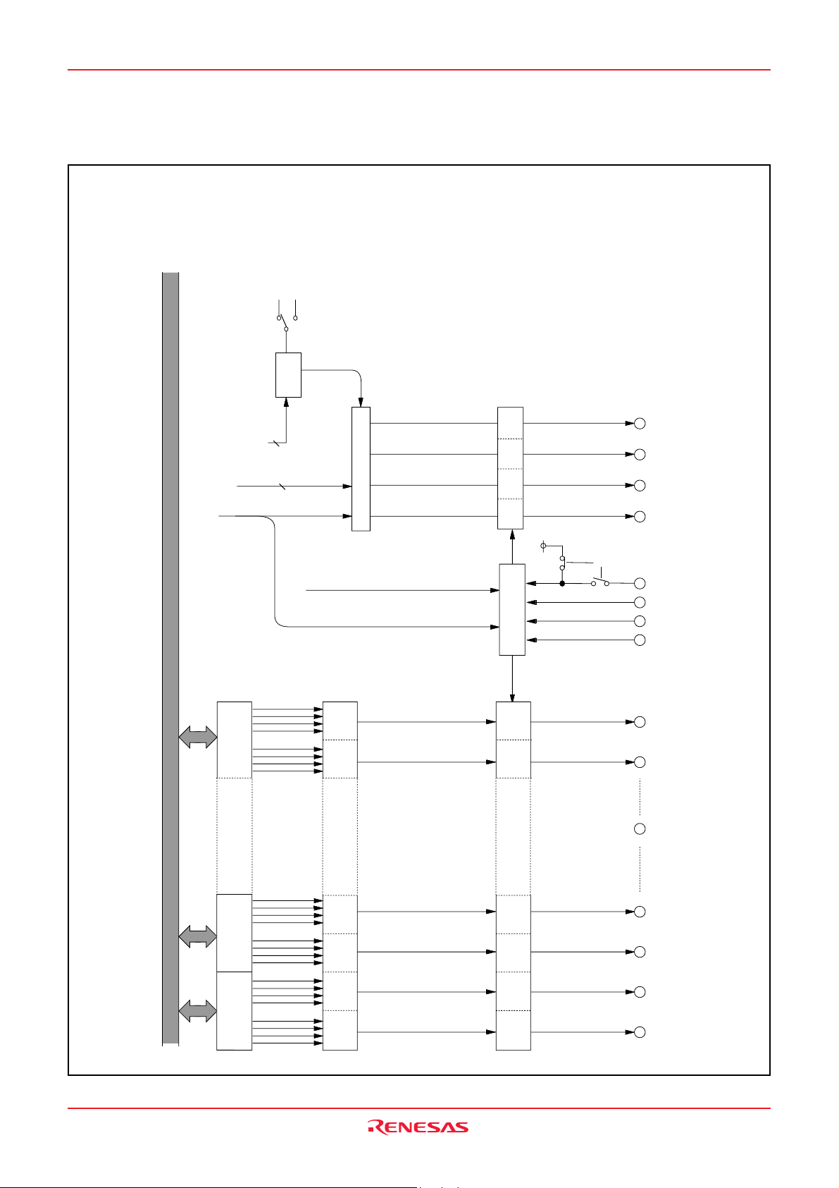
3823 Group
C
O
M
0
O
M
1
C
O
M
2
C
O
M
3
V
S
S
V
L
1
V
L
2
L
3
E
G
3
E
G
2
S
E
G
1
S
E
G
0
“
1
”
0
”
L
C D C
K
2
2
1
7
/
S
E
G
3
1
P
1
6
/
S
E
G
3
0
3
4
/
S
E
G
1
2
f
( S U B ) / 3
2
f
(
X
I
N
)
/ 8 1 9 2 ( o r f ( S U B ) / 8 1 9 2 i n
l
o w - s p e e d m o d e
)
a
t
a
b
u
s
A
d d r e s
s
0
0 4
0
1
6
d
d
r
e
s
s
0
4
1
1
6
A
d d r e s
s
0
0 4
F
1
6
S
e l e c t o
r
S
e l e c t o
r
S
e l e c t o
r
S
e l e c t o
r
S
e l e c t o
r
S
e l e c t o
r
S
e g m e n t r i v e
r
S
e g m e n
t
d
r i v e
r
e
g
m
e
n
t
r
i
v
e
r
S
e g m e n
t
d
r i v e
r
S
e g m e n t r i v e
r
S
e g m e n t r i v e
r
i
a
s
c
o
n
t
r
o
l
L
C
D
d
i v i d e
r
i
m
i
n
g
c
o
n
t
r
o
l
l
e
r
C
o m m o n r i v e
r
u
t
y
r
a
t
i
o
s
e
l
e
c
t
i
o
n
b
i
t
s
C
o m m o n r i v e
r
C
o m m o
n
d
r i v e
r
o
m
m
o
n
r
i
v
e
r
B
i a s c o n t r o l b i
t
L
C D c i r c u i t d i v i d e
r
d
i v i s i o n r a t i o s e l e c t i o n b i t
s
L
C D C K c o u n t s o u r c
e
s
e l e c t i o n b i
t
L
C D d i s p l a y R A
M
C
D
e
n
a
b
l
e
b
i
t
V
C
C
L
C
D
e
n a b l e b i
t
N
o t e :
f
( S U B ) i s t h e s o u r c e o s c i l l a t i o n f r e q u e n c y i n l o w - s p e e d m o d e . f ( S U B ) s h o w s t h e o s c i l l a t i o n f r e q u e n c y o f
X
C
I
N
o r t h e o n - c h i p o s c i l l a t o r
.
Fig. 37 Block diagram of LCD controller/driver
Rev.2.02 Jun 19, 2007 page 41 of 73
REJ03B0146-0202
Page 42

3823 Group
Bias Control and Applied Voltage to LCD
Power Input Pins
To the LCD power input pins (VL1–VL3), apply the voltage shown
in Table 11 according to the bias value.
Select a bias value by the bias control bit (bit 2 of the LCD mode
register).
Common Pin and Duty Ratio Control
The common pins (COM0–COM3) to be used are determined by
duty ratio.
Select duty ratio by the duty ratio selection bits (bits 0 and 1 of the
LCD mode register).
Contrast control
Table 11 Bias control and applied voltage to VL1–VL3
Bias value
VL3=VLCD
1/3 bias
1/2 bias
Note 1: VLCD is the maximum value of supplied voltage for the
LCD panel.
Table 12 Duty ratio control and common pins used
Duty
ratio
2
3
4
Notes1: COM2 and COM3 are open.
2: COM
VL2=2/3 VLCD
VL1=1/3 VLCD
VL3=VLCD
VL2=VL1=1/2 VLCD
Duty ratio selection bit
Bit 1 Bit 0
0
1
1
3 is open.
1
0
1
Voltage value
Common pins used
COM0, COM1 (Note 1)
COM0–COM2 (Note 2)
COM0–COM3
Contrast control
V
L3
R 1
V
L 2
R2
V
L1
R 3
R 1 = R 2 = R 3
Fig. 38 Example of circuit at each bias
V
L3
R 4
V
L 2
V
L1
R 5
R 4 = R 5
1 / 2 b i a s1 / 3 b i a s
Rev.2.02 Jun 19, 2007 page 42 of 73
REJ03B0146-0202
Page 43

3823 Group
LCD Display RAM
Address 004016 to 004F16 is the designated RAM for the LCD display. When “1” are written to these addresses, the corresponding
segments of the LCD display panel are turned on.
B i t
A d d r e s s
0040
0041
0042
0043
0044
0045
0046
0047
0048
0049
004A
004B
004C
004D
004E
004F
7
16
16
16
16
16
16
16
16
16
16
16
16
16
16
16
16
COM
3
COM
SEG
SEG
SEG
SEG
SEG
SEG
SEG
SEG
SEG
SEG
SEG
SEG
SEG
SEG
SEG
SEG
2
1
3
5
7
9
11
13
15
17
19
21
23
25
27
29
31
COM
LCD Drive Timing
The LCDCK timing frequency (LCD drive timing) is generated internally and the frame frequency can be determined with the
following equation;
(frequency of count source for LCDCK)
(divider division ratio for LCD)
f(LCDCK)
(duty ratio)
01
0
2
4
6
8
10
12
14
16
18
20
22
24
26
28
30
COM
0
1
3
2
COM
SEG
SEG
SEG
SEG
SEG
SEG
SEG
SEG
SEG
SEG
SEG
SEG
SEG
SEG
SEG
SEG
2
COM
1
f(LCDCK) =
Frame frequency =
3456
COM
0
COM
Fig. 39 LCD display RAM map
STP Instruction Execution
Execution of the STP instruction sets the LCD enable bit (bit 3 of
the LCD mode register) to “0” and the LCD panel turns off.To
make the LCD panel turn on after returning from the stop mode,
set the LCD enable bit to “1”.
Rev.2.02 Jun 19, 2007 page 43 of 73
REJ03B0146-0202
Page 44
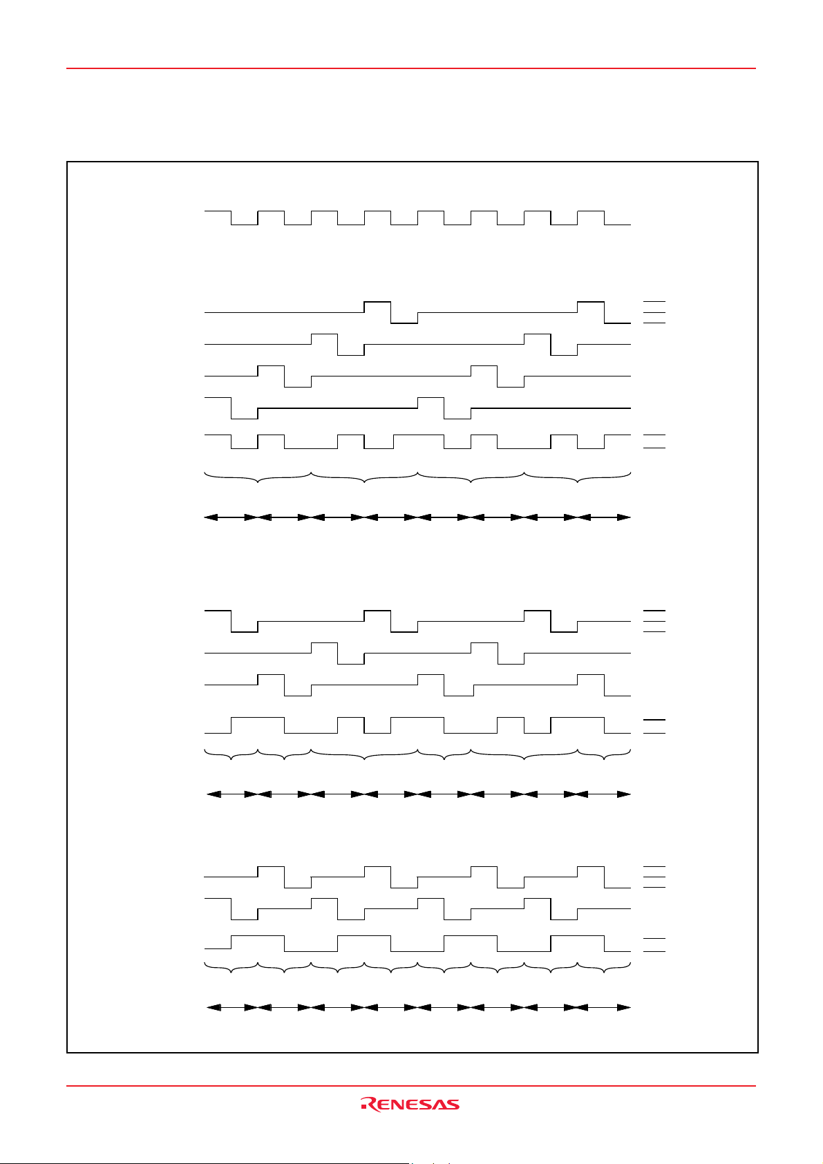
3823 Group
I n t e r n a l l o g i c
L C D C K t i m i n g
1 / 4 d u t y
C O M
C O M
C O M
C O M
S E G
1 / 3 d u t y
C O M
COM
Voltage level
V
L 3
V
L 2
= V
0
1
2
3
0
O F FO
C O M
3
COM2COM
0
1
N OFF O N
COM
1
COM
0
3
C O M2C O M1C O M
0
V
SS
V
L 3
V
S S
V
L 3
VL2=V
V
SS
L 1
L1
C O M
2
SEG
0
C O M0C O M2C O M
1 / 2 d u t y
C O M
0
C O M
1
S E G
0
C O M1C O M0C O M
Fig. 40 LCD drive waveform (1/2 bias)
O F FO N O NOFFO NO
COM
1
0
C O M2C O M
1
C O M0C O M
F
F
2
OFFON OFFON OFFON OFFON
COM
1
0
C O M1C O M
0
C O M1C O M
0
V
L 3
V
SS
V
L3
V
L 2
= V
L 1
V
S S
V
L 3
V
S S
Rev.2.02 Jun 19, 2007 page 44 of 73
REJ03B0146-0202
Page 45

3823 Group
I n t e r n a l l o g i c
L C D C K t i m i n g
1 / 4 d u t y
C O M
COM
C O M
C O M
SEG
1 / 3 d u t y
COM
C O M
V o l t a g e l e v e l
V
L 3
V
0
1
2
3
0
O F FON O F FO
COM
3
COM
2
COM1COM
0
1
COM
0
3
COM
2
N
COM1COM
0
L 2
V
L 1
V
S S
V
L 3
V
S S
V
L 3
V
L 2
V
L 1
V
SS
C O M
2
SEG
0
C O M
0
COM
1/2 duty
C O M
0
C O M
1
SEG
0
C O M1C O M
Fig. 41 LCD drive waveform (1/3 bias)
OFFO N ON OFF O NOFF
2
COM1COM
C O M2C O M1C O M0C O M
0
2
OFFO N O F FO N O F FO N OFFO N
0
C O M1C O M
C O M1C O M0C O M1C O M
0
0
V
L3
V
SS
V
L3
V
L 2
V
L 1
V
SS
V
L 3
V
S S
Rev.2.02 Jun 19, 2007 page 45 of 73
REJ03B0146-0202
Page 46

3823 Group
R A M
R A M
A
F
F
ROM CORRECTION FUNCTION
A part of program in ROM can be corrected.
Set the start address of the corrected ROM data (i.e. an Op code
address of the beginning instruction) to the ROM correction address low-order and high-order registers. The program for the
correction is stored in RAM for ROM correction.
When the program is being executed and the value of the program
counter matches with the set address value in the the ROM correction address registers,the program is branched to the start
address of RAM for ROM correction and then the correction program is executed. Use the JMP instruction (3-byte instruction) to
return the main program from the correction program.
The correctable area is up to two. There are two blocks of RAM for
ROM correction:
Block 1: Address 0A0016
Block 2: Address 0A2016
The ROM correction function is controlled by the ROM correction
enable register.
If the ROM correction function is not used, the ROM correction
vector may be used as normal RAM. When using the ROM correction vector as normal RAM, make sure to set bits 1 and 0 in the
ROM correction enable register to “0” (Disable).
Notes 1:When using the ROM correction function, set the ROM
correction address registers and then enable the ROM
correction with the ROM correction enable register.
2: Do not set addresses other than the ROM area in the
ROM correction address registers.
Do not set the same addresses in both the ROM correction address 1 registers and the ROM correction address
2 registers.
3: It is necessary to contain the process in the program to
transfer the correction program from an external
EEPROM and others to the RAM for ROM correction.
ROM correction address 1 high-order register (RCA1H)
ROM correction address 1 low-order register (RCA1L)
ROM correction address 2 high-order register (RCA2H)
ROM correction address 2 low-order register (RCA2L)
Note: Do not set addressed other than the ROM area.
Fig. 42 ROM correction address register
1 f o r R O M c o r r e c t i o
2 f o r R O M c o r r e c t i o
Fig. 43 RAM for ROM correction
0 0 1 01
6
0 0 1 11
6
001216
001316
0016
0
n
0A1
16
0A2016
n
0A3
16
b 7b
( N o t e
0
R O M c o r r e c t i o n e n a b l e r e g i s t e r ( A d d r e s s 0 0 1 41
R C R
A d d r e s s 1 e n a b l e b i t ( R C 0 )
0 : D i s a b l e
1 : E n a b l e
A d d r e s s 2 e n a b l e b i t ( R C 1 )
0 : D i s a b l e
1 : E n a b l e
N o t u s e d ( r e t u r n s “ 0 ” w h e n r e a d )
N o t e : S e t t h e R O M c o r r e c t i o n a d d r e s s r e g i s t e r s b e f o r e e n a b l i n g t h e R O M c o r r e c t i o n w i t h t h e
R O M c o r r e c t i o n e n a b l e r e g i s t e r .
Fig. 44 Structure of ROM correction enable register
Rev.2.02 Jun 19, 2007 page 46 of 73
REJ03B0146-0202
6)
)
Page 47

3823 Group
φφ
φ CLOCK SYSTEM OUTPUT FUNCTION
φφ
The internal system clock φ or XCIN frequency signal can be output from port P41 by setting the φ output control register. Set bit 1
of the port P4 direction register to “1” when outputting φ clock.
Set the bit 4 in the peripheral function expansion register to “1”
when the XCIN frequency signal is output.
b 7
b 0
φ output control register
(CKOUT : address 002A
φ output control bit
0 : port function
1 : φ clock output or X
Not used (return “0” when read)
Fig. 45 Structure of
φφ
φ output control register
φφ
Temporary data register
The temporary data register (addresses 002C16 to 002E16) is the
8-bit register and does not have the control function. It can be
used to store data temporarily. It is initialized after reset.
b7 b0
16
)
CIN
frequency signal output
RRF register
The RRF register (address 002F16)is the 8-bit register and does
not have the control function. As for the value written in this register, high-order 4 bits and low-order 4 bits interchange. It is
initialized after reset.
T e m p o r a r y d a t a r e g i s t e r 0 , 1 , 2
1 6
, 0 0 2 D
1 6
, 0 0 2 E
1 6
( A d d r e s s : 0 0 2 C
TD0,TD1,TD
2
)
b 7b
Fig. 46 Structure of temporary register, RPF register
0
d a t a s t o r a g e
D B
D B
1
d a t a s t o r a g e
D B
2
d a t a s t o r a g e
D B
3
d a t a s t o r a g e
D B
4
d a t a s t o r a g e
D B
5
d a t a s t o r a g e
D B
6
d a t a s t o r a g e
D B
7
d a t a s t o r a g e
0
R R F r e g i s t e r ( A d d r e s s : 0 0 2 F
R R F R
4
d a t a s t o r a g e
D B
D B
5
d a t a s t o r a g e
D B
6
d a t a s t o r a g e
D B
7
d a t a s t o r a g e
D B
0
d a t a s t o r a g e
D B
1
d a t a s t o r a g e
D B
2
d a t a s t o r a g e
D B
3
d a t a s t o r a g e
1 6
)
Rev.2.02 Jun 19, 2007 page 47 of 73
REJ03B0146-0202
Page 48

3823 Group
WATCHDOG TIMER
The watchdog timer gives a mean of returning to the reset status
when a program cannot run on a normal loop (for example, because of a software run-away). The watchdog timer consists of an
8-bit counter.
Initial Value of Watchdog Timer
At reset or writing to the watchdog timer control register, each
watchdog timer is set to “FF16.” Instructions such as STA, LDM
and CLB to generate the write signals can be used.
The written data in bits 0 to 5 are not valid, and the above values
are set.
Bits 7 and 6 can be rewritten only once after reset.
After rewriting it is disable to write any data to this bit. These bits
become “0” after reset.
Standard Operation of Watchdog Timer
The watchdog timer is in the stop state at reset and the watchdog
timer starts to count down by writing an optional value in the
watchdog timer control register. An internal reset occurs at an underflow of the watchdog timer. Then, reset is released after the
reset release time is elapsed, the program starts from the reset
vector address. Normally, writing to the watchdog timer control
register before an underflow of the watchdog timer is programmed. If writing to the watchdog timer control register is not
On-chip oscillator
X
CIN
Internal system clock
selection bit (bit 7 of
the CPU mode register)
X
IN
RESET
On-chip oscillator mode
control bit
“0”
“1”
STP instruction bit
1/1024
1/4
Undefined instruction
STP instruction
Watchdog timer count
source selection bit
“0”
“1”
Reset
executed, the watchdog timer does not operate.
When reading the watchdog timer control register is executed, the
contents of the high-order 6-bit counter and the STP instruction bit
(bit 6), and the count source selection bit (bit 7) are read out.
Bit 6 of Watchdog Timer Control Register
• When bit 6 of the watchdog timer control register is “0”, the MCU
enters the stop mode by execution of STP instruction.
Just after releasing the stop mode, the watchdog timer restarts
counting (Note). When executing the WIT instruction, the watchdog timer does not stop.
• When bit 6 is “1”, execution of STP instruction causes an internal
reset. When this bit is set to “1” once, it cannot be rewritten to
“0” by program. Bit 6 is “0” at reset.
The time until the underflow of the watchdog timer register after
writing to the watchdog timer control register is executed is as follows (when the bit 7 of the watchdog timer control register is “0”) ;
• at frequency/2/4/8 mode (f(XIN)) = 8 MHz): 32.768 ms
• at low-speed mode (f(XCIN) = 32 KHz): 8.19s
■ Note
The watchdog timer continues to count even during the wait time set
by timer 1 and timer 2 to release the stop state and in the wait
mode. Accordingly, do not underflow the watchdog timer in this time.
Data bus
Watchdog timer
L (2)
Watchdog timer
Wait until reset release
Reset
circuit
H (6)
“FF16” is set when
watchdog timer control
register is written to.
Internal reset
Fig. 47 Block diagram of Watchdog timer
b7 b0
Watchdog timer control register (Address 003716)
WDTCON
Watchdog timer H (for read-out of high-order 6 bit)
“FF
16” is set to watchdog timer by writing to these bits.
STP instruction function selection bit
0: Entering stop mode by execution of STP instruction
1: Internal reset by execution of STP instruction
Watchdog timer count source selection bit
0: f(X
IN)/1024 (f(SUB)/1024 at low-speed mode)
1: f(X
IN)/4 (f(SUB)/1024 at low-speed mode)
Fig. 48 Structure of Watchdog timer control register
N
f ( XI
)
I n t e r n a l r e s e t
s i g n a l
W a t c h d o g t i m e r
d e t e c t i o n
Fig. 49 Timing of reset output
Rev.2.02 Jun 19, 2007 page 48 of 73
REJ03B0146-0202
Note : Bits 6 and 7 can be rewritten only once after reset.
After rewriting it is disable to write any data to this bit.
f (
= 8 M
s e c
= 3 2m
(
XI
N)
HZ)
Page 49

3823 Group
PERIPHERAL FUNCTION EXTENSION REGISTER
The serial I/O transfer direction can be switched by setting the bit
0 in the peripheral function expansion register to “1”. This function
is valid only when the bit 6 in the serial I/O control register is set to
“1” (when the clock synchronous serial I/O is selected). P47 can
be selected as the output pin of the clock synchronous serial I/O
by setting the bit 1 in the peripheral function expansion register to
“1”. When setting P47 to the SOUT pin, set the bit 7 in the port P4
direction register to “1”. This function is valid only when the bit 6 in
the serial I/O control register to “1” (when the clock synchronous
serial I/O is selected). P-channel output of TXD and SOUT can be
disabled by the bits 2 and 3 in the peripheral function expansion
register. Set the bit 4 in the UART control register to “1” after selecting the pin to disable the P-channel output. XCIN frequency
signal can be output from the port P41 by setting the bit 4 in the
peripheral function expansion register to “1”. Set the bit 0 in the φ
output control register and the bit 1 in the port P4 direction register to “1” to output the XCIN frequency signal.
b 7b
0
Peripheral function ext ens ion register (A ddr ess: 003016)
EXP
Transfer direction selection bit (valid when UART is used)
0 : LSB first
1 : MSB first
Synchronous serial I/O output pin selection bit
0:P4
1:P4
P-channel output disabled selection bit
00: P4
01: The bit 4 in the UART control register is invalid
10: P4
11: P4
Output clock selection bit
0: φ clock output
1: X
Not used (returns “0” when read)
(Do not write “1” to this bit)
Fig. 50 Structure of peripheral function extension register
5/TX
7/SRDY/SOUT
5/TX
5/TX
7/SRDY/SOUT
CIN
frequency signal output
D pin
pin
D pin
D pin or P47/S
pin
RDY/SOUT
pin
Rev.2.02 Jun 19, 2007 page 49 of 73
REJ03B0146-0202
Page 50

3823 Group
RESET CIRCUIT
To reset the microcomputer, RESET pin should be held at an “L”
level for 2 µs or more. Then the RESET pin is returned to an “H”
level (the power source voltage should be between VCC(min.) and
5.5 V, and the quartz-crystal oscillator should be stable), reset is
released. After the reset is completed, the program starts from the
address contained in address FFFD16 (high-order byte) and address FFFC16 (low-order byte). Make sure that the reset input
voltage meets VIL spec. when a power source voltage passes
VCC(min.).
P o w e r
s o u r c e
R E S E T
R E S E T
V
C C
V
C C
v o l t a g e
0 V
R e s e t i n p u t
v o l t a g e
0 V
Fig. 51 Reset Circuit Example
P o w e r o n
V
I L
s p e c .
P o w e r s o u r c e v o l t a g e
d e t e c t i o n c i r c u i t
IN
X
φ
R E S E T
I n t e r n a l
r e s e t
A d d r e s s
D a t a
S Y N C
Fig. 52 Reset Sequence
????
N :
b o u t 8 0 0 0 c y c l e
XI
a
a n d f
= 8 • f
N o t e s 1 : T h e f r e q u e n c y r e l a t i o n o f f ( XI
2 : T h e q u e s t i o n m a r k s ( ? ) i n d i c a t e a n u n d e f i n e d s t a t e t h a t d e p e n d s o n t h e p r e v i o u s s t a t e .
s
N)
(φ) i s f ( XI
N)
(φ)
F F F CF F F D
ADL
R e s e t a d d r e s s f r o m
v e c t o r t a b l e
A D
H , A
DL
ADH
Rev.2.02 Jun 19, 2007 page 50 of 73
REJ03B0146-0202
Page 51

3823 Group
( 1 )
P o r t P 0 d i r e c t i o n r e g i s t e r
( 2 )
P o r t P 1 d i r e c t i o n r e g i s t e r
( 3 )
P o r t P 2 d i r e c t i o n r e g i s t e r
( 4 )
P o r t P 4 d i r e c t i o n r e g i s t e r
( 5 )
P o r t P 5 d i r e c t i o n r e g i s t e r
( 6 )
P o r t P 6 d i r e c t i o n r e g i s t e r
( 7 )
P o r t P 7 d i r e c t i o n r e g i s t e r
( 8 )
R O M c o r r e c t o i n e n a b l e r e g i s t e r ( R C R )
( 9 )
P U L L r e g i s t e r A
( 1 0 )
P U L L r e g i s t e r B
( 1 1 )
S i r i a l I / O s t a t u s r e g i s t e r
( 1 2 )
S i r i a l I / O c o n t r o l r e g i s t e r
( 1 3 )
U A R T c o n t r o l r e g i s t e r
( 1 4 )
T i m e r X h i g h - o r d e r r e g i s t e r
( 1 5 )
T i m e r X l o w - o r d e r r e g i s t e r
( 1 6 )
T i m e r Y h i g h - o r d e r r e g i s t e r
( 1 7 )
T i m e r Y l o w - o r d e r r e g i s t e r
( 1 8 )
T i m e r 1 r e g i s t e r
( 1 9 )
T i m e r 2 r e g i s t e r
( 2 0 )
T i m e r 3 r e g i s t e r
( 2 1 )
T i m e r X m o d e r e g i s t e r
( 2 2 )
T i m e r Y m o d e r e g i s t e r
( 2 3 )
T i m e r 1 2 3 m o d e r e g i s t e r
( 2 4 )
φ o u t p u t c o n t r o l r e g i s t e r
( 2 5 )
C P U m o d e e x t e n s i o n r e g i s t e r
( 2 6 )
Te m p o r a r y d a t a r e g i s t e r 0
( 2 7 )
T e m p o r a r y d a t a r e g i s t e r 1
( 2 8 )
T e m p o r a r y d a t a r e g i s t e r 2
( 2 9 )
R R F r e g i s t e r
( 3 0 )
P e r i p h e r a l f u n c t i o n e x t e n s i o n r e g i s t e r
( 3 1 )
A D c o n t r o l r e g i s t e r
( 3 2 )
A D c o n v e r s i o n l o w - o r d e r r e g i s t e r
( 3 3 )
W a t c h d o g t i m e r c o n t r o l r e g i s t e r
( 3 4 )
S e g m e n t o u t p u t e n a b l e r e g i s t e r
( 3 5 )
L C D m o d e r e g i s t e r
( 3 6 )
I n t e r r u p t e d g e s e l e c t i o n r e g i s t e r
( 3 7 )
C P U m o d e r e g i s t e r
( 3 8 )
I n t e r r u p t r e q u e s t r e g i s t e r 1
( 3 9 )
I n t e r r u p t r e q u e s t r e g i s t e r 2
( 4 0 )
I n t e r r u p t c o n t r o l r e g i s t e r 1
( 4 1 )
I n t e r r u p t c o n t r o l r e g i s t e r 2
( 4 2 )
P r o c e s s o r s t a t u s r e g i s t e r
( 4 3 )
P r o g r a m c o u n t e r
Address
0001
0003
0005
0009
000B
000D
000F
0014
0016
0017
0019
001A
001B
0020
0021
0022
0023
0024
0025
0026
0027
0028
0029
002A
002B
002C
002D
002E
002F
0030
0034
0036
0037
0038
0039
003A
003B
003C
003D
003E
003F
(PS)
(PC
(PC
R e g i s t e r C o n t e n t s
0 0
0 0
0 0
0 0
0 0
0 0
0 0
0 0
0 0
0 0
F F
F F
F F
F F
F F
0 1
F F
0 0
0 0
0 0
0 0
0 0
0 0
0 0
0 0
0 0
0 0
0 0
0 0
0 0
0 0
0 0
0 0
0 0
1 6
1 6
1 6
1 6
1 6
1 6
1 6
1 6
1 6
1 6
1 6
1 6
1 6
1 6
1 6
1 6
1 6
1 6
1 6
1 6
1 6
1 6
1 6
1 6
1 6
1 6
1 6
1 6
1 6
1 6
1 6
1 6
1 6
1 6
1
16
16
16
16
16
16
16
16
0 0001 110
16
16
1 0000 000
16
16
16
1 1100 000
16
16
16
16
16
16
16
16
16
16
16
16
16
16
16
16
16
0 0001 000
16
✕✕
16
00111 111
16
16
16
16
01001 000
16
16
16
16
16
000 000
✕✕✕✕✕ ✕✕
H
)
L
)
C o n t e n t s o f a d d r e s s F F F D
C o n t e n t s o f a d d r e s s F F F C
1 6
1 6
Note: The contents of all other registers and RAM are undefined after reset, so they must be
initialized by software.
✕: undefined
Fig. 53 Initial status of microcomputer after reset
Rev.2.02 Jun 19, 2007 page 51 of 73
REJ03B0146-0202
Page 52

3823 Group
CLOCK GENERATING CIRCUIT
The 3823 group has two built-in oscillation circuits. An oscillation
circuit can be formed by connecting a resonator between XIN and
XOUT (XCIN and XCOUT). Use the circuit constants in accordance
with the resonator manufacturer's recommended values. The oscillation start voltage and the oscillation start time differ in
accordance with an oscillator, a circuit constant, or temperature,
etc.
When power supply voltage is low and the high frequency oscillator is used, an oscillation start will require sufficient conditions. No
external resistor is needed between XIN and XOUT since a feedback resistor exists on-chip. (an external feed-back resistor may
be needed depending on conditions.) However, an external feedback resistor is needed between XCIN and XCOUT since a resistor
does not exist between them.
To supply a clock signal externally, input it to the XIN pin and make
the XOUT pin open. The sub-clock XCIN-XCOUT oscillation circuit
cannot directly input clocks that are externally generated. Accordingly, be sure to cause an external resonator to oscillate.
Immediately after poweron, only the XIN oscillation circuit starts
oscillating, and XCIN and XCOUT pins function as I/O ports.
X
CINXCOUT
Rf
C
CIN
Note : Insert a damping resistor if required. The resistance will vary
depending on the oscillator and the oscillation drive capacity
setting. Use the value recommended by the maker of the
oscillator. Also, if the oscillator manufacturer's data sheet
specifies that a feedback resistor be added external to the chip
though a feedback resistor exists on-chip, insert a feedback
resistor between X
Rd
C
COUT
IN
and X
XINX
OUT
Rd
C
IN
C
OUT
OUT
following the instruction.
Frequency Control
(1) frequency/8 Mode
The internal clock φ is the frequency of XIN divided by 8.
After reset, this mode is selected.
(2) frequency/4 Mode
The internal clock φ is the frequency of XIN divided by 4.
(3) frequency/2 Mode
The internal clock φ is half the frequency of XIN.
(4) Low-speed Mode
●The internal clock φ is the frequency of XIN or on-chip oscillation
frequency divided by 2.
●A low-power consumption operation can be realized by stopping
the main clock XIN in this mode. To stop the main clock, set bit 5
of the CPU mode register to “1”.
When the main clock XIN is restarted, set enough time for oscillation to stabilize by programming.
In low speed mode, the system clock φ can be switched to the
on-chip oscillator or XCIN. Use the on-chip oscillator control bit
(bit 0 in the CPU mode expansion register) for settings. To set
this bit to “0” from “1”, wait until XCIN oscillation stabilizes.
Note 1: If you switch the mode between frequency/2/4/8 mode
and low-speed, stabilize both XIN and XCIN oscillations.
The sufficient time is required for the sub-clock to stabilize, especially immediately after poweron and at
returning from stop mode. When switching the mode between middle/high-speed and low-speed, set the
frequency on condition that f(XIN) > 3f(XCIN).
2: In frequency/2/4/8 mode, XIN-XOUT oscillation does not
stop even if the main clock (XIN-XOUT) stop bit is set to
"1".
3: In low speed mode, XCIN-XCOUT oscillation does not stop
even if the port XC switch bit is set to "0".
Fig. 54 Ceramic resonator circuit example
X
C I N
X
Rf
C O U T
Rd
X
X
O U T
I N
Open
E x t e r n a l o s c i l l a t i o n c i r c u i t
C
C
C I N
C O U T
C C
V
V
S S
Fig. 55 External clock input circuit
Rev.2.02 Jun 19, 2007 page 52 of 73
REJ03B0146-0202
Page 53

3823 Group
Oscillation Control
(1) Stop Mode
If the STP instruction is executed, the internal clock φ stops at an
“H” level, and XIN and XCIN oscillators stop. Timer 1 is set to
“FF16” and timer 2 is set to “0116”.
Either XIN or XCIN divided by 16 is input to timer 1 as count
source, and the output of timer 1 is connected to timer 2. The bits
of the timer 123 mode register except bit 4 are cleared to “0”. Set
the timer 1 and timer 2 interrupt enable bits to disabled (“0”) before executing the STP instruction. Oscillator restarts at reset or
when an external interrupt is received, but the internal clock φ is
not supplied to the CPU until timer 2 underflows. This allows timer
for the clock circuit oscillation to stabilize.
Execution of the STP instruction sets the LCD enable bit (bit 3 of
the LCD mode register) to “0” and the LCD panel turns off.To
make the LCD panel turn on after returning from the stop mode,
set the LCD enable bit to “1”.
On-chip
oscillator
(Note 2)
Q
S
XCOUT
“1”
“0”
Port XC
switch bit
On-chip oscillator
control bit
Internal system clock selection bit
“1”
“0”
Frequency/2/4/8
mode
Main clock stop bit
(Note 1)
Low-speed mode
1/2
1/2
Frequency/4
mode
control bit
1/4
Frequency/2/4
mode or lowspeed mode
XCIN
XIN XOUT
(2) Wait Mode
If the WIT instruction is executed, only the system clock φ stops at
an "H" state. The states of main clock, on-chip oscillator and sub
clock are the same as the state before executing the WIT instruction, and oscillation does not stop. Since supply of system clock φ
is started immediately after the interrupt is received, the instruction can be executed immediately.
f(SUB)
Timer 1
count source
selection bit
“1”
1/2
Main clock division
ratio selection bit
“1”
“0”
S
“0”
Frequency/8 mode
Q
Q
Timer 1
S
Timer 2
count source
selection bit
“0”
“1”
Timing φ
(Internal system clock)
Timer 2
R
STP instruction
Reset
Interrupt disable flag 1
Interrupt request
Notes 1: When using the low-speed mode, set the port X
2: Although a feed-back resistor exists on-chip, an external feed-back resistor may be needed depending
on conditions.
Fig. 56 Clock generating circuit block diagram
Rev.2.02 Jun 19, 2007 page 53 of 73
REJ03B0146-0202
WIT
instruction
R
C
switch bit to “1” .
STP instruction
R
Page 54

3823 Group
Rese
t
b7 b4
CM
Frequency/8 mode (f(φ) = 1 MHz)
CM7 = 0 (8 MHz selected)
CM6 = 1 (Frequency/8)
CM5 = 0 (8 MHz oscillating)
CM4 = 0 (Stopped)
“0”
4
CM
“1”
Frequency/8 mode (f(φ) = 1 MHz)
CM7 = 0 (8 MHz selected)
CM6 = 1 (frequency/8)
CM5 = 0 (8 MHz oscillating)
CM4 = 1 (Oscillating)
or EXPCM0 = 1
(On-chip oscillator oscillation)
CM
“1”
6
“0”“1”
“0”
4
6
CM
“1”
CM
“1”
“0”
6
“0”“1”
“0”
7
CM
“1”
Low-speed mode (f(SUB)/2)
7
= 1 (32 kHz or on-chip
CM
oscillator selected)
CM6 = 1 (Middle-speed)
5
= 0 (8 MHz oscillating)
CM
CM4 = 1 (Oscillating)
“0”
5
CM
“1”
Low-power dissipation mode
(f(SUB)/2)
7
= 1 (32 kHz or on-chip
CM
oscillator selected)
CM6 = 1 (Middle-speed)
CM5 = 1 (8 MHz stopped)
4
= 1 (Oscillating)
CM
Notes
1 : Switch the mode by the allows shown between the mode blocks. (Do not switch between the mode directly without an allow.)
2 : The all modes can be switched to the stop mode or the wait mode and returned to the source mode when the stop mode or the wait mode is ended.
3 : Timer and LCD operate in the wait mode.
4 : When the stop mode is ended, a delay of approximately 1 ms occurs automatically by timer 1 and timer 2 in frequency/2/4/8 mode.
5 : When the stop mode is ended, a delay of approximately 0.25 s occurs automatically by timer 1 and timer 2 in low-speed mode.
6 : Wait until oscillation stabilizes after oscillating the main clock X
7 : The example assumes that 8 MHz is being applied to the X
8 : f(SUB) is the source oscillation frequency in low-speed mode. f(SUB) shows the oscillation frequency of X
Internal clock φ is f(SUB)/2 in the low-speed mode.
9 : Set the CPU mode expansion register in advance when switching to low-speed mode which uses mode divided by 4 and on-chip oscillator.
10: In low speed mode, the system clock φ can be switched to the on-chip oscillator or X
expansion register) for settings. To set this bit to "0" from "1", wait until X
CM
CM
6
“0”“1”
“0”
5
6
“1”
CM
“1”
“0”
“1”
6
CM
“0”“1”
Frequency/2 mode (f(φ) = 4 MHz)
or frequency/4 mode (f(φ) = 2 MHz)
CM
4
CM
6
“1”“0”
“0”
Frequency/2 mode (f(φ) = 4 MHz)
or frequency/4 mode (f(φ) = 2 MHz)
CM7 = 0 (8 MHz selected)
CM6 = 0 (Frequency/2/4)
CM
CM4 = 1 (Oscillating)
CM
“0”
5
CM
6
“1”
“0”
CM
7
= 0 (8 MHz selected)
CM6 = 0 (Frequency/2/4)
CM5 = 0 (8 MHz oscillating)
CM4 = 0 (Stopped)
“0”
4
CM
“1”
5
= 0 (8 MHz oscillating)
or EXPCM0 = 1
(On-chip oscillator oscillation)
“0”
7
CM
“1”
Low-speed mode (f(SUB)/2)
7
= 1 (32 kHz or on-chip
CM
oscillator selected)
CM6 = 0 (High-speed)
CM5 = 0 (8 MHz oscillating)
CM4 = 1 (Oscillating)
“0”
5
CM
“1”
Low-power dissipation mode
(f(SUB)/2)
7
= 1 (32 kHz or on-chip
CM
oscillator selected)
CM6 = 0 (high-speed)
CM5 = 1 (8 MHz stopped)
4
= 1 (Oscillating)
CM
IN
before the switching from the low-speed mode to frequency/2/4/8 mode.
IN
pin and 32 kHz to the X
Note 1 : The on-chip oscillator is selected for the operation clock
in low-speed mode regardless of X
2 : Valid only when the main clock division ratio selection bit
(bit 6 in the CPU mode register) is set to "0".
When "1" (frequency/8 mode) is selected for the main clock
division ratio selection bit or when the internal system clock
selection bit is set to 1, set "0" to the frequency/4 mode control bit.
b7 b4
Note 1 : In low speed mode (X
X
CIN-XCOUT
is set to "0".
2 : In frequency/2/4/8 mode, X
the main clock (X
3 : When the system clock φ is divided by 4 of f(X
the CPU mode register to “0” after setting the bit 1 in the CPU
mode extension register to “1”.
4 : When using the on-chip oscillator in low-speed mode, set the bit 7
in the CPU mode register to “1” after setting the bit 0 in the CPU
mode extension register to “1”.
CIN
pin. φ indicates the internal clock.
CIN
CIN
oscillation stabilizes.
. Use the on-chip oscillator control bit (bit 0 in the CPU mode
CPU mode extension register
(EXPCM : address: 002B
On-chip oscillator control bit
0 : On-chip oscillator not used
(on-chip oscillator stopping)
1 : On-chip oscillator used (Note 1)
(on-chip oscillator oscillating)
Frequency/4 mode control bit (Note 2)
(Valid only when high-speed mode)
0 : Frequency/2 mode φ = f(X
1 : Frequency/4 mode φ = f(X
Not used (returns “0” when read)
(Do not write “1” to this bit)
CPU mode register
(CPUM : address 003B
4
: Port Xc switch bit (Note 1)
CM
0: I/O port (Oscillation stopped)
CIN
, X
COUT
1: X
5
:Main clock (XIN–X
CM
0: Oscillating
1: Stopped
6
:Main clock division ratio selection bit
CM
0: f(X
or f(X
1: f(X
7
:Internal system clock selection bit
CM
0: X
1: X
(low-speed mode) (Note 4)
oscillating function
OUT
IN
)/2 (frequency/2 mode),
IN
)/4 (frequency/4 mode) (Note 3)
IN
)/8 (frequency/8 mode)
IN–XOUT
selected (frequency/2/4/8 mode)
CIN–XCOUT
, or on-chip oscillator selected
CIN
is selected as the system clock φ),
16
CIN-XCOUT
16
)
) stop bit (Note 2)
oscillation does not stop even if the port XC switch bit
IN-XOUT
IN-XOUT
CIN
or the on-chip oscillator.
oscillation does not stop even if
) stop bit is set to "1".
,)
IN
)/2
IN
)/4
.
IN
), set the bit 6 in
Fig. 57 State transitions of system clock
Rev.2.02 Jun 19, 2007 page 54 of 73
REJ03B0146-0202
Page 55

3823 Group
QzROM Writing Mode
In the QzROM writing mode, the user ROM area can be rewritten
while the microcomputer is mounted on-board by using a serial
programmer which is applicable for this microcomputer.
Table 13 lists the pin description (QzROM writing mode) and Figure 58 and Figure 59 show the pin connections.
Refer to Figure 60 and Figure 61 for examples of a connection
with a serial programmer.
Contact the manufacturer of your serial programmer for serial programmer. Refer to the user’s manual of your serial programmer
for details on how to use it.
Table 13 Pin description (QzROM writing mode)
Pin
VCC, VSS
RESET
XIN
XOUT
VREF
AVSS
P00 –P07
P10 –P17
P20 –P27
P34 –P37
P41–P44
P50 –P57
P60 –P67
P40
P44
P42
P43
Name
Power source
Reset input
Clock input
Clock output
Analog reference voltage
Analog power source
I/O port
VPP input
ESDA input/output
ESCLK input
ESPGMB input
I/O
Input
Input
Input
Output
Input
Input
I/O
Input
I/O
Input
Input
Function
• Apply 1.8 to 5.5 V to VCC, and 0 V to VSS.
•Reset input pin for active “L”. Reset occurs when RESET pin is hold at an “L” level
for 16 cycles or more of XIN.
•Set the same termination as the single-chip mode.
• Input the reference voltage of A/D converter to VREF.
•Connect AVss to Vss.
• Input “H” or “L” level signal or leave the pin open.
• QzROM programmable power source pin.
• Serial data I/O pin.
• Serial clock input pin.
• Read/program pulse input pin.
Rev.2.02 Jun 19, 2007 page 55 of 73
REJ03B0146-0202
Page 56

3823 Group
)
8
SEG
9
SEG
10
SEG
11
SEG
12
/SEG
4
P3
13
/SEG
5
P3
14
/SEG
6
P3
15
/SEG
7
P3
16
/SEG
0
P0
17
/SEG
1
P0
18
/SEG
2
P0
19
/SEG
3
P0
20
/SEG
4
P0
21
/SEG
5
P0
22
/SEG
6
P0
23
/SEG
7
P0
24
/SEG
0
P1
25
/SEG
1
P1
26
/SEG
2
P1
27
/SEG
3
P1
28
/SEG
4
P1
29
/SEG
5
P1
30
/SEG
6
P1
31
/SEG
7
P1
V
CC
GND
SEG7
SEG6
SEG5
SEG4
SEG3
SEG2
SEG1
SEG0
VREF
AV
COM3
COM2
COM1
COM0
VCC
VL3
65
66
67
68
69
70
71
72
73
74
75
SS
76
77
78
79
80
M3823XGX-XXXFP
M3823XGXFP
123456789101112131415161718192021222324
2
VL
4
5
6
/AN
6
P6
/AN
5
P6
/AN
4
P6
3
/AN
3
P6
2
/AN
2
P6
7
1
VL
/AN
7
P6
PRQP0080GB-A (80P6N-A)
Fig. 58 Pin connection diagram (M3823XGX-XXXFP)
15
14
13
12
11
10
SEG
SEG
/SEG
4
P3
/SEG
5
P3
/SEG
6
P3
/SEG
7
P3
0
1
/AN
/AN
0
1
P6
P6
ESPGMB
16
17
/SEG
/SEG
0
1
P0
P0
/ADT
7
P5
18
/SEG
2
P0
OUT
/T
6
P5
19
/SEG
3
P0
1
/CNTR
5
P5
ESDA
20
/SEG
4
P0
1
0
/RTP
3
/CNTR
4
P5
P5
21
/SEG
5
P0
0
/RTP
2
P5
22
/SEG
6
P0
3
/INT
1
P5
23
/SEG
7
P0
2
/INT
0
P5
24
/SEG
0
P1
OUT
/S
RDY
/S
7
P4
25
/SEG
1
P1
CLK
/S
6
P4
26
/SEG
2
P1
D
X
/T
5
P4
27
/SEG
3
P1
D
X
/R
4
P4
28
/SEG
4
P1
414243444546474849505152535455565758596061626364
1
/INT
3
P4
29
/SEG
5
P1
0
/INT
2
P4
40
P20/KW0
39
P21/KW1
38
P22/KW2
37
P23/KW3
36
P24/KW4
35
P25/KW5
34
P26/KW6
33
P27/KW7
32
VSS
31
XOU
30
XIN
T
29
P70/XCOUT
28
P71/XCIN
27
RESET
26
25
P4
P41/φ
0
GND
*
VPP
RESET
*: Connect to oscillation circuit.
: QzROM pin
ESCLK
60
59
58
57
56
55
M3823XGX-XXXHP
M3823XGXHP
2
5
4
3
6
2
3
4
5
6
/AN
/AN
/AN
/AN
/AN
2
3
4
5
6
P6
P6
P6
P6
P6
V
CC
GND
SEG
SEG
SEG
SEG
SEG
SEG
SEG
SEG
SEG
SEG
V
AV
COM
COM
COM
COM
61
9
62
8
63
7
64
6
65
5
66
4
67
3
68
2
1
69
70
0
V
CC
71
72
REF
SS
73
3
74
2
75
1
76
0
77
V
L3
78
V
L2
79
V
L1
80
1
7
/AN
7
P6
ESDA
PLQP0080KB-A (80P6Q-A
Fig. 59 Pin connection diagram (M3823XGX-XXXHP)
54
7
1
/AN
1
P6
8
53
0
/AN
0
P6
52
9
/ADT
7
P5
10
51
OUT
/T
6
P5
50
11
1
/CNTR
5
P5
49
48
13
12
1
0
/RTP
3
/CNTR
4
P5
P5
47
14
0
/RTP
2
P5
46
15
3
/INT
1
P5
16
45
2
/INT
0
P5
41
42
44
43
40
P16/SEG
39
38
37
36
35
34
33
32
31
30
29
28
27
26
25
24
23
22
21
20
19
18
17
D
D
X
X
CLK
OUT
/T
/R
/S
5
/S
4
6
P4
P4
P4
RDY
/S
7
P4
30
P17/SEG
31
P20/KW
0
P21/KW
1
P22/KW
2
P23/KW
3
P24/KW
4
P25/KW
5
P26/KW
6
P27/KW
7
V
SS
X
OUT
X
IN
P70/X
P71/X
RESET
0
P4
P41/φ
P42/INT
P43/INT
COUT
CIN
0
1
*
*: Connect to oscillation circuit.
: QzROM pin
GND
RESET
ESCLK
V
PP
ESPGMB
Rev.2.02 Jun 19, 2007 page 56 of 73
REJ03B0146-0202
Page 57

3823 Group
V c c
4 . 7 kΩ
4 . 7 kΩ
3 8 2 3 G r o u p
V c c
P 4
0
P 4
4
( E S D A )
2
( E S C L K )
P 4
3
(ESPGMB)
P4
RESET
14
1 2
1 0
8
6
4
2
1 3
1 1
9
7
5
3
1
circuit
*1
R E S E T
Vss
A V s s
I N
X
X
OUT
Set the same termination as
the single-chip mode.
1
: Open-collector buffer
*
Note: For the programming circuit, the wiring capacity of each signal pin must not exceed 47 pF.
Fig. 60 When using E8 programmer, connection example
Rev.2.02 Jun 19, 2007 page 57 of 73
REJ03B0146-0202
Page 58

3823 Group
3 8 2 3 G r o u p
T _ V D D
T _ V P P
T _ T X D
T_RXD
T _ S C L K
T_BUSY N.C.
T _ P G M / O E / M D
RESET circuit
T_RESET
4.7 kΩ
4 . 7 kΩ
Vcc
0
P4
P44 (ESDA)
2
(ESCLK)
P4
P4
3
(ESPGMB)
RESET
G N D
Note: For the programming circuit, the wiring capacity of each signal pin must not exceed 47 pF.
Fig. 61 When using programmer of Sisei Electronics System Co., LTD, connection example
Rev.2.02 Jun 19, 2007 page 58 of 73
REJ03B0146-0202
Vss
AVss
X
S e t t h e s a m e t e r m i n a t i o n a s t h e
s i n g l e - c h i p m o d e .
I N
X
OUT
Page 59

3823 Group
NOTES ON PROGRAMMING
Processor Status Register
The contents of the processor status register (PS) after a reset are
undefined, except for the interrupt disable flag (I) which is “1”. After a reset, initialize flags which affect program execution.
In particular, it is essential to initialize the index X mode (T) and
the decimal mode (D) flags because of their effect on calculations.
Initialize these flags at the beginning of the program.
Interrupt
The contents of the interrupt request bits do not change immediately after they have been written. After writing to an interrupt
request register, execute at least one instruction before performing a BBC or BBS instruction.
Decimal Calculations
•To calculate in decimal notation, set the decimal mode flag (D)
to “1”, then execute an ADC or SBC instruction. After executing
an ADC or SBC instruction, execute at least one instruction before executing a SEC, CLC, or CLD instruction.
• In decimal mode, the values of the negative (N), overflow (V),
and zero (Z) flags are invalid.
Timers
If a value n (between 0 and 255) is written to a timer latch, the frequency division ratio is 1/(n + 1).
A/D Converter
The comparator is constructed linked to a capacitor. The conversion accuracy may be low because the charge is lost if the
conversion speed is not enough. Accordingly, set f(XIN) to at least
500kHz during A/D conversion in the middle-or high-speed mode.
Also, do not execute the STP or WIT instruction during an A/D
conversion.
In the low-speed mode, since the A/D conversion is executed by
the on-chip oscillator, the minimum value of f(XIN) frequency is not
limited.
LCD Drive Control Circuit
Execution of the STP instruction sets the LCD enable bit (bit 3 of
the LCD mode register) to “0” and the LCD panel turns off.To
make the LCD panel turn on after returning from the stop mode,
set the LCD enable bit to “1”.
Instruction Execution Time
The instruction execution time is obtained by multiplying the frequency of the internal clock φ by the number of cycles needed to
execute an instruction.
The number of cycles required to execute an instruction is shown
in the list of machine instructions.
The frequency of the internal clock φ is half of the XIN frequency.
Multiplication and Division Instructions
The index mode (T) and the decimal mode (D) flags do not affect
the MUL and DIV instruction.
The execution of these instructions does not change the contents
of the processor status register.
Ports
The contents of the port direction registers cannot be read.
The following cannot be used:
• The data transfer instruction (LDA, etc.)
• The operation instruction when the index X mode flag (T) is “1”
• The addressing mode which uses the value of a direction register as an index
• The bit-test instruction (BBC or BBS, etc.) to a direction register
• The read-modify-write instruction (ROR, CLB, or SEB, etc.) to a
direction register
Use instructions such as LDM and STA, etc., to set the port direction registers.
Serial Interface
In clock synchronous serial I/O, if the receive side is using an external clock and it is to output the SRDY signal, set the transmit
enable bit, the receive enable bit, and the SRDY output enable bit
to “1”.
Serial I/O continues to output the final bit from the TXD pin after
transmission is completed.
Rev.2.02 Jun 19, 2007 page 59 of 73
REJ03B0146-0202
Page 60

3823 Group
Countermeasures against noise
(1) Shortest wiring length
➀ Wiring for RESET pin
Make the length of wiring which is connected to the RESET pin
as short as possible. Especially, connect a capacitor across the
RESET pin and the VSS pin with the shortest possible wiring
(within 20mm).
● Reason
The width of a pulse input into the RESET pin is determined by
the timing necessary conditions. If noise having a shorter pulse
width than the standard is input to the RESET pin, the reset is
released before the internal state of the microcomputer is completely initialized. This may cause a program runaway.
Noise
Reset
circuit
V
SS
N.G.
Reset
circuit
RESET
SS
V
RESET
Noise
X
IN
X
OUT
V
SS
N.G.
Fig. 63 Wiring for clock I/O pins
(2) Connection of bypass capacitor across VSS line and VCC line
In order to stabilize the system operation and avoid the latch-up,
connect an approximately 0.1 µF bypass capacitor across the VSS
line and the VCC line as follows:
• Connect a bypass capacitor across the VSS pin and the VCC pin
at equal length.
• Connect a bypass capacitor across the VSS pin and the VCC pin
with the shortest possible wiring.
• Use lines with a larger diameter than other signal lines for VSS
line and VCC line.
• Connect the power source wiring via a bypass capacitor to the
VSS pin and the VCC pin.
O.K.
X
X
V
IN
OUT
SS
SS
V
O.K.
Fig. 62 Wiring for the RESET pin
➁ Wiring for clock input/output pins
• Make the length of wiring which is connected to clock I/O pins
as short as possible.
• Make the length of wiring (within 20 mm) across the grounding
lead of a capacitor which is connected to an oscillator and the
VSS pin of a microcomputer as short as possible.
• Separate the VSS pattern only for oscillation from other VSS
patterns.
● Reason
If noise enters clock I/O pins, clock waveforms may be deformed. This may cause a program failure or program runaway.
Also, if a potential difference is caused by the noise between
the VSS level of a microcomputer and the VSS level of an oscillator, the correct clock will not be input in the microcomputer.
SS
V
V
V
CC
V
SS
CC
V
SS
N.G. O.K.
Fig. 64 Bypass capacitor across the VSS line and the VCC line
Rev.2.02 Jun 19, 2007 page 60 of 73
REJ03B0146-0202
Page 61

3823 Group
( N
)
( N
)
( N
)
( N
)
(3) Oscillator concerns
In order to obtain the stabilized operation clock on the user system
and its condition, contact the oscillator manufacturer and select
the oscillator and oscillation circuit constants. Be careful especially when range of votage and temperature is wide.
Also, take care to prevent an oscillator that generates clocks for a
microcomputer operation from being affected by other signals.
➀ Keeping oscillator away from large current signal lines
Install a microcomputer (and especially an oscillator) as far as
possible from signal lines where a current larger than the tolerance of current value flows.
● Reason
In the system using a microcomputer, there are signal lines for
controlling motors, LEDs, and thermal heads or others. When a
large current flows through those signal lines, strong noise occurs because of mutual inductance.
➁ Installing oscillator away from signal lines where potential levels
change frequently
Install an oscillator and a connecting pattern of an oscillator
away from signal lines where potential levels change frequently.
Also, do not cross such signal lines over the clock lines or the
signal lines which are sensitive to noise.
● Reason
Signal lines where potential levels change frequently (such as
the CNTR pin signal line) may affect other lines at signal rising
edge or falling edge. If such lines cross over a clock line, clock
waveforms may be deformed, which causes a microcomputer
failure or a program runaway.
➀ Keeping oscillator away from large current signal lines
Microcomputer
Mutual inductance
M
X
Large
current
IN
X
OUT
V
SS
GND
➁ Installing oscillator away from signal lines where potential
levels change frequently
Do not cross
CNTR
IN
X
X
OUT
V
SS
(4) Analog input
The analog input pin is connected to the capacitor of a voltage
comparator. Accordingly, sufficient accuracy may not be obtained
by the charge/discharge current at the time of A/D conversion
when the analog signal source of high-impedance is connected to
an analog input pin. In order to obtain the A/D conversion result
stabilized more, please lower the impedance of an analog signal
source, or add the smoothing capacitor to an analog input pin.
(5) Difference of memory size
When memory size differ in one group, actual values such as an
electrical characteristics, A/D conversion accuracy, and the amount
of -proof of noise incorrect operation may differ from the ideal values.
When these products are used switching, perform system evaluation for each product of every after confirming product specification.
(6) Wiring to P40/(VPP) pin
When using P40/(VPP) pin as an input port, connect an approximately
5 kΩ resistor to the P40/(VPP) pin the shortest possible in series.
When not using P40/(VPP) pin, connect the pin the shortest possible to the GND pattern which is supplied to the Vss pin of the
microcomputer. In addition connecting an approximately 5 kΩ re-
sistor in series to the GND could improve noise immunity. In this
case as well as the above mention, connect the pin the shortest
possible to the GND pattern which is supplied to the Vss pin of the
microcomputer.
● Reason
The P40/(VPP) pin of the QzROM version is the power source input pin
for the built-in QzROM. When programming in the QzROM, the impedance of the VPP pin is low to allow the electric current for writing to
flow into the built-in QzROM. Because of this, noise can enter easily. If
noise enters the P40/(VPP) pin, abnormal instruction codes or data are
read from the QzROM, which may cause a program runaway.
(1) When using P40/(VPP) pin as an input port
T h e s h o r t e s t
A p p r o x . 5 kΩ
P 40/ ( V
P P
)
o t e
o t e
S S
V
(2) When not using P40/(VPP) pin
T h e s h o r t e s t
P 40/ ( V
o t e
P P
)
A p p r o x . 5 kΩ
o t e
S S
V
T h e s h o r t e s t
N.G.
Fig. 65 Wiring for a large current signal line/
Wiring of signal
Fig. 66 Wiring for the P40/(VPP) pin
N o t e . S h o w s t h e m i c r o c o m p u t e r ' s p i n .
lines where potential levels change frequently
Rev.2.02 Jun 19, 2007 page 61 of 73
REJ03B0146-0202
Page 62

3823 Group
g
NOTES ON USE
Power Source Voltage
When the power source voltage value of a microcomputer is less
than the value which is indicated as the recommended operating
conditions, the microcomputer does not operate normally and may
perform unstable operation.
In a system where the power source voltage drops slowly when
the power source voltage drops or the power supply is turned off,
reset a microcomputer when the power source voltage is less than
the recommended operating conditions and design a system not
to cause errors to the system by this unstable operation.
LCD drive power supply
Power supply capacitor may be insufficient with the division resistance for LCD power supply,and the characteristic of the LCD panel.In
this case,there is the method of connecting the bypass capacitor
about 0.1 –0.33µF to VL1 –VL3 pins.The example of a strengthening
measure of the LCD drive power supply is shown in Figure 67.
L 3
V
V
L 2
V
L1
•C o n n e c t b y t h e s h o r t e s t
p o s s i b l e w i r i n g .
•C o n n e c t t h e b y p a s s c a p a c i t o r
t o t h e V
L 1
– V
L 3
a s p o s s i b l e .
( R e f e r e n t i a l v a l u e : 0 . 1 – 0 . 3 3
p i n s a s s h o r t
µ
F )
3823 Group
Fig. 67
Strengthening measure example of LCD drive power supply
Product shipped in blank
As for the product shipped in blank, Renesas does not perform the
writing test to user ROM area after the assembly process though
the QzROM writing test is performed enough before the assembly
process. Therefore, a writing error of approx.0.1 % may occur.
Moreover, please note the contact of cables and foreign bodies on a
socket, etc. because a writing environment may cause some writing errors.
NOTES ON QzROM
Notes On QzROM Writing Orders
When ordering the QzROM product shipped after writing, submit
the mask file (extension: .msk) which is made by the mask file
converter MM.
Be sure to set the ROM option ("MASK option" written in the mask
file converter) setup when making the mask file by using the mask
file converter MM.
Notes On ROM Code Protect
(QzROM product shipped after writing)
As for the QzROM product shipped after writing, the ROM code
protect is specified according to the ROM option setup data in the
mask file which is submitted at ordering.
The ROM option setup data in the mask file is “0016” for protect
enabled or “FF16” for protect disabled. Therefore, the contents of
the ROM code protect address (other than the user ROM area) of
the QzROM product shipped after writing is “0016” or “FF16”.
Note that the mask file which has nothing at the ROM option data
or has the data other than “0016” and “FF16” can not be accepted.
DATA REQUIRED FOR QzROM WRITING
ORDERS
The following are necessary when ordering a QzROM product
shipped after writing:
1. QzROM Writing Confirmation Form*
2. Mark Specification Form*
3. ROM data...........Mask file
* For the QzROM writing confirmation form and the mark specification form, refer to the “Renesas Technology Corp.” Homepage
(http://www.renesas.com).
Note that we cannot deal with special font marking (customer's
trademark etc.) in QzROM microcomputer.
Overvoltage
Make sure that voltage exceeding the Vcc pin voltage is not applied to other pins. In particular, ensure that the state indicated by
bold lines in figure below does not occur for pin P40 (VPP power
source pin for QzROM) during power-on or power-off. Otherwise
the contents of QzROM could be rewritten.
~
1.8V
V
CC
pin voltage
P40 pin voltage
“H” input
0
pin voltage
P4
“L” input
(1) Input voltage to other MCU pins rises before Vcc pin voltage.
(2) Input voltage to other MCU pins falls after Vcc pin voltage.
Note: The internal circuitry is unstable when Vcc is below the minimum voltage specification of 1.
8 V (shaded portion), so particular care should be exercised re
Fig. 68
Timing Diagram (Applies to section indicated by bold line.)
Rev.2.02 Jun 19, 2007 page 62 of 73
REJ03B0146-0202
~
~
~
~
~
1.8V
arding overvoltage.
Page 63
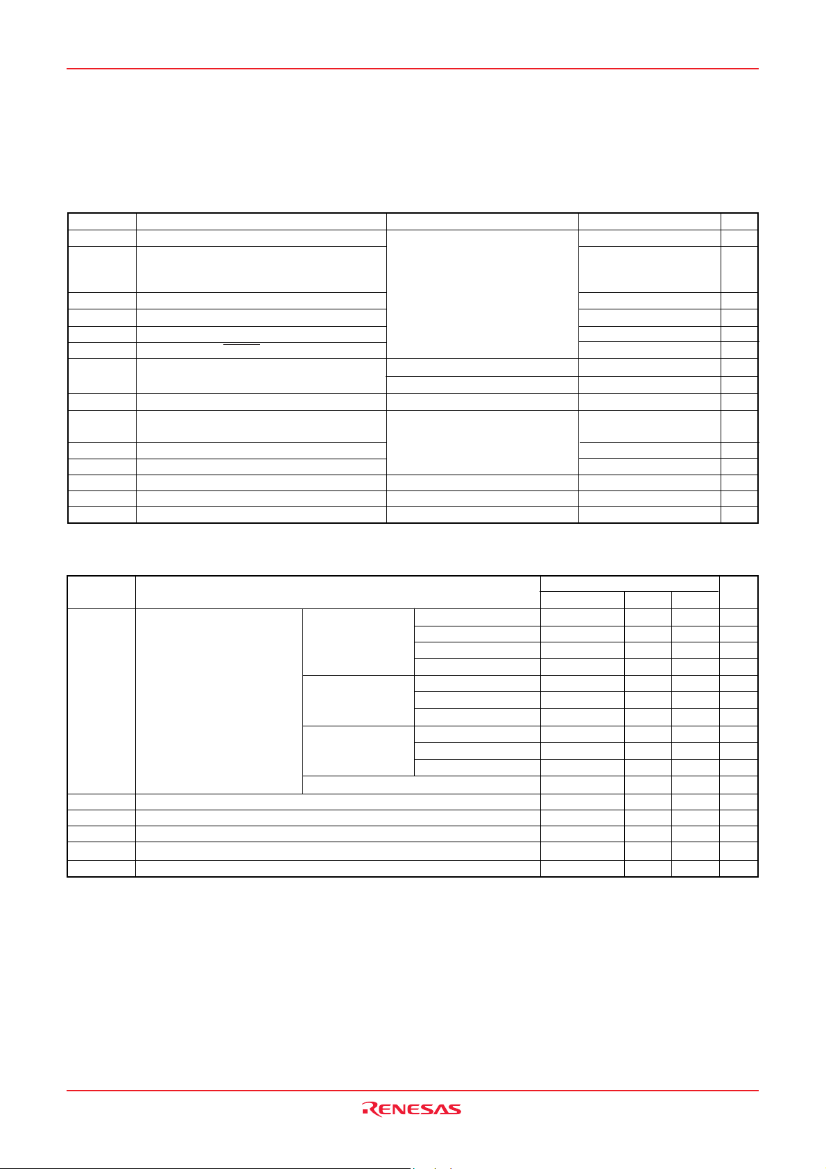
3823 Group
ELECTRICAL CHARACTERISTICS
Table 14 Absolute maximum ratings
Symbol Parameter Conditions Ratings Unit
VCC
VI
VI
VI
VI
VI
VO
VO
VO
VO
VO
Pd
Topr
Tstg
Input voltage P00–P07, P10–P17, P20–P27,
P34–P37, P40–P47, P50–P57
P60–P67, P70, P71
Input voltage VL1
Input voltage VL2
Input voltage VL3
Input voltage RESET, XIN
Output voltage P00–P07, P10–P17
Output voltage P34–P37
Output voltage P20–P27, P41–P47,P50–P57,
P60–P67, P70, P71
Output voltage SEG0–SEG11
Output voltage XOUT
Power dissipation
Operating temperature
Storage temperature
All voltages are based on VSS.
When an input voltage is measured, output transistors are cut
off.
At output port
At segment output
At segment output
Ta = 25°C
–0.3 to 6.5 VPower source voltage
–0.3 to VCC +0.3
–0.3 to VL2
VL1 to VL3
VL2 to 6.5
–0.3 to VCC +0.3
–0.3 to VCC +0.3
–0.3 to VL3
–0.3 to VL3
–0.3 to VCC +0.3
–0.3 to VL3
–0.3 to VCC +0.3
300
–20 to 85
–40 to 150
V
V
V
V
V
V
V
V
V
V
V
mW
°C
°C
Table 15 Recommended operating conditions (1)
(VCC = 1.8 to 5.5 V, Ta = –20 to 85 °C, unless otherwise noted)
Symbol Parameter
VCC
VSS
VL 3
VREF
AVSS
VIA
Note : When the A/D converter is used, refer to the recommended operating condition for A/D converter.
Power source voltage
(Note 1)
Power source voltage
LCD power voltage
A/D conversion reference voltage
Analog power source voltage
Analog input voltage AN0–AN7
Frequency/2 mode f(XIN) = 10 MHz
f(XIN) = 8 MHz
f(XIN) = 5 MHz
f(XIN) = 2.5 MHz
Frequency/4 mode f(XIN) = 10 MHz
f(XIN) = 8 MHz
f(XIN) = 5 MHz
Frequency/8 mode f(XIN) = 10 MHz
f(XIN) = 8 MHz
f(XIN) = 5 MHz
Low-speed mode (OCO included)
Min.
4.5
4.0
2.0
1.8
2.5
2.0
1.8
2.5
2.0
1.8
1.8
2.5
1.8
AVSS
Limits
Typ. Max.
5.0
5.0
5.0
5.0
5.0
5.0
5.0
5.0
5.0
5.0
5.0
0
0
5.5
5.5
5.5
5.5
5.5
5.5
5.5
5.5
5.5
5.5
5.5
5.5
VCC
VREF
Unit
V
V
V
V
V
V
V
V
V
V
V
V
V
V
V
V
Rev.2.02 Jun 19, 2007 page 63 of 73
REJ03B0146-0202
Page 64

3823 Group
Table 16 Recommended operating conditions (2)
(VCC = 1.8 to 5.5 V, Ta = –20 to 85 °C, unless otherwise noted)
Symbol Parameter
VIH
VIH
VIH
VIH
VIL
VIL
VIL
VIL
“H” input voltage P00–P07, P10–P17,P34–P37, P40, P41, P45, P47, P52,
P53,P56,P60–P67,P70,P71 (CM4= 0)
“H” input voltage P20–P27, P42–P44,P46,P50, P51, P54, P55, P57
“H” input voltage RESET
“H” input voltage XIN
“L” input voltage P00–P07, P10–P17,P34–P37, P40, P41, P45, P47, P52, P53,
P56,P60–P67,P70,P71 (CM4= 0)
“L” input voltage P20–P27, P42–P44,P46,P50, P51, P54, P55, P57
“L” input voltage RESET
“L” input voltage XIN
Min.
0.7VCC
0.8VCC
0.8VCC
0.8VCC
0
0
0
0
Limits
Typ. Max.
VCC
VCC
VCC
VCC
0.3 VCC
0.2 VCC
0.2 VCC
0.2 VCC
Unit
V
V
V
V
V
V
V
V
Rev.2.02 Jun 19, 2007 page 64 of 73
REJ03B0146-0202
Page 65

3823 Group
Table 17 Recommended operating conditions (3)
(VCC = 1.8 to 5.5 V, Ta = –20 to 85 °C, unless otherwise noted)
Symbol Parameter
ΣIOH(peak)
ΣIOH(peak)
ΣIOL(peak)
ΣIOL(peak)
ΣIOH(avg)
ΣIOH(avg)
ΣIOL(avg)
ΣIOL(avg)
IOH(peak)
IOH(peak)
“H” total peak output current
“H” total peak output current
“L” total peak output current
“L” total peak output current
“H” total average output current
“H” total average output current
“L” total average output current
“L” total average output current
“H” peak output current
“H” peak output current
P00–P07, P10–P17, P20–P27 (Note 1)
P41–P47, P50–P57, P60–P67, P70, P71 (Note 1)
P00–P07, P10–P17, P20–P27 (Note 1)
P41–P47, P50–P57, P60–P67, P70, P71 (Note 1)
P00–P07, P10–P17, P20–P27 (Note 1)
P41–P47, P50–P57, P60–P67, P70, P71 (Note 1)
P00–P07, P10–P17, P20–P27 (Note 1)
P41–P47, P50–P57, P60–P67, P70, P71 (Note 1)
P00–P07, P10–P17 (Note 2)
P20–P27, P41–P47, P50–P57, P60–P67, P70, P71
Min.
(Note 2)
IOL(peak)
IOL(peak)
“L” peak output current
“L” peak output current
P00–P07, P10–P17 (Note 2)
P20–P27, P41–P47, P50–P57, P60–P67, P70, P71
(Note 2)
IOH(avg)
IOH(avg)
“H” average output current
“H” average output current
P00–P07, P10–P17 (Note 3)
P20–P27, P41–P47, P50–P57, P60–P67, P70, P71
(Note 3)
IOL(avg)
IOL(avg)
f(CNTR0)
f(CNTR1)
“L” average output current
“L” average output current
Input frequency for timers X and Y
(duty cycle 50%)
P00–P07, P10–P17 (Note 3)
P20–P27, P41–P47, P50–P57, P60–P67, P70, P71
(Note 3)
(4.5 V ≤ VCC ≤ 5.5 V)
(4.0 V ≤ VCC ≤ 4.5 V)
(2.0 V ≤ VCC ≤ 4.0 V)
(VCC ≤ 2.0 V)
f(XIN)
Main clock input oscillation frequency
(duty cycle 50%)
(Note 4)
Frequency/2 mode
(4.5 V ≤ VCC ≤ 5.5 V)
Frequency/2 mode
(4.0 V ≤ VCC ≤ 4.5 V)
Frequency/2 mode
(2.0 V ≤ VCC ≤ 4.0 V)
Frequency/2 mode
(1.8 V ≤ VCC ≤ 2.0 V)
Frequency/4 mode
(2.5 V ≤ VCC ≤ 5.5 V)
Frequency/4 mode
(2.0 V ≤ VCC ≤ 2.5 V)
Frequency/4 mode
(1.8 V ≤ VCC ≤ 2.0 V)
Frequency/8 mode
(2.5 V ≤ VCC ≤ 5.5 V)
Frequency/8 mode
(2.0 V ≤ VCC ≤ 2.5 V)
Frequency/8 mode
(1.8 V ≤ VCC ≤ 2.0 V)
f(XCIN)
Sub-clock input oscillation frequency
(duty cycle 50%)
(Note 5)
Notes 1: The total output current is the sum of all the currents flowing through all the applicable ports. The total average current is an average value
measured over 100 ms. The total peak current is the peak value of all the currents.
2: The peak output current is the peak current flowing in each port.
3: The average output current is an average value measured over 100 ms.
4: When the A/D converter is used, refer to the recommended operating condition for A/D converter.
5: When using the microcomputer in low-speed mode, make sure that the sub-clock input oscillation frequency on condition that f(X
Limits
Typ. Max.
–40
–40
–20
–20
–1.0
–2.5
2 ✕ VCC – 4
0.75 ✕ VCC + 1
6.25 ✕ VCC - 10
4 ✕ VCC – 8
1.5 ✕ VCC + 2
12.5 ✕ VCC - 20
4 ✕ V
15 ✕ VCC – 22
4 ✕ V
15 ✕ VCC – 22
32.768
40
40
20
20
–2
–5
5
10
2.5
5.0
5.0
10.0
10.0
CC
10.0
CC
80
CIN) < f(XIN)/3.
Unit
mA
mA
mA
mA
mA
mA
mA
mA
mA
mA
mA
mA
mA
mA
mA
mA
MHz
MHz
MHz
MHz
MHz
MHz
MHz
MHz
MHz
MHz
MHz
MHz
MHz
MHz
kHz
Rev.2.02 Jun 19, 2007 page 65 of 73
REJ03B0146-0202
Page 66
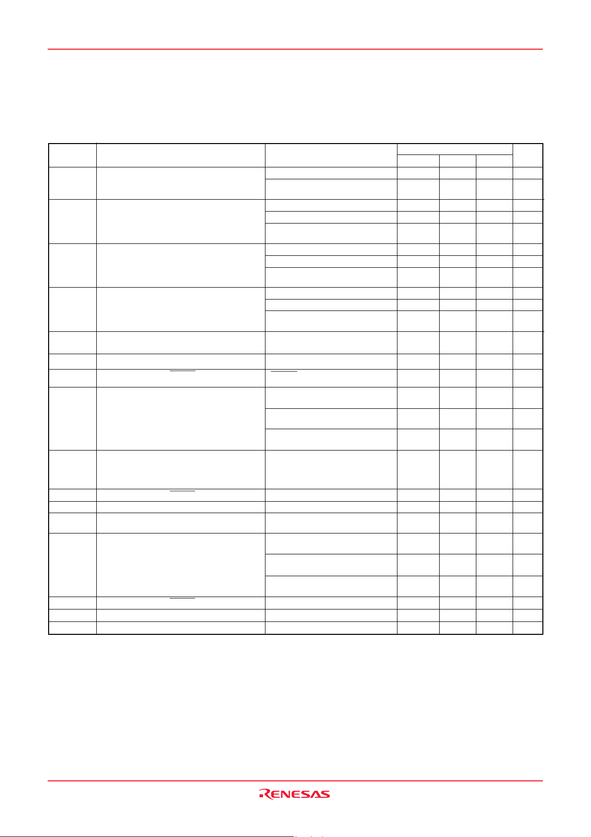
3823 Group
Table 18 Electrical characteristics (1)
(VCC = 4.0 to 5.5 V, Ta = –20 to 85 °C, unless otherwise noted)
Symbol Parameter
VOH
VOH
VOL
VOL
VT+ – VT–
VT+ – VT–
VT+ – VT–
IIH
IIH
“H” output voltage
P00–P07, P10–P17
“H” output voltage
P20–P27, P41–P47, P50–P57, P60–P67,
P70, P71 (Note)
“L” output voltage
P00–P07, P10–P7
“L” output voltage
P20–P27, P41–P47, P50–P57, P60–P67,
P70, P71 (Note)
Hysteresis
INT0–INT3, ADT , CNTR0, CNTR1, P20–P27
Hysteresis SCLK, RXD
Hysteresis RESET
“H” input current
P00–P07, P10–P17, P34–P37
“H” input current
P20–P27, P40–P47, P50–P57, P60–P67,
P70, P71 (Note)
Test conditions
IOH = –2.5 mA
IOH = –0.6 mA
VCC = 2.5 V
IOH = –5 mA
IOH = –1.25 mA
IOH = –1.25 mA
VCC = 2.5 V
IOL = 5 mA
IOL = 1.25 mA
IOL = 1.25 mA
VCC = 2.5 V
IOL = 10 mA
IOL = 2.5 mA
IOL = 2.5 mA
VCC = 2.5 V
RESET : VCC = 2.0 V to 5.5 V
VI = VCC
Pull-downs “off”
VCC = 5 V, VI = VCC
Pull-downs “on”
VCC = 3 V, VI = VCC
Pull-downs “on”
VI = VCC
Min.
VCC–1.0
VCC–2.0
VCC–0.5
VCC–1.0
30
6.0
Limits
Typ. Max.
0.5
0.5
0.5
70
25
Unit
2.0
0.5
2.0
0.5
5.0 µA
140
45
5.0
VVCC–2.0
V
V
V
V
V
V
V1.0
V
V
V1.0
V
V
V
µA
µA
µA
IIH
IIH
IIL
IIL
IIL
IIL
VRAM
Note: When “1” is set to the port XC switch bit (bit 4 at address 003B16) of CPU mode register, the drive ability of port P70 is different from the value above
mentioned.
“H” input current RESET
“H” input current XIN
“L” input current
P00–P07, P10–P17, P34–P37,P40
“L” input current
P20–P27, P41–P47, P50–P57, P60–P67,
P70, P71 (Note)
“L” input current RESET
“L” input current XIN
RAM hold voltage
VI = VCC
VI = VCC
VI = VSS
VI = VSS
Pull-ups “off”
VCC = 5 V, VI = VSS
Pull-ups “on”
VCC = 3 V, VI = VSS
Pull-ups “on”
VI = VSS
VI = VSS
When clock is stopped
–30
–6.0
1.8
4.0
–70
–25
–4.0
5.0
–5.0
–5.0
–140
–45
–5.0
5.5
µA
µA
µA
µA
µA
µA
µA
µA
V
Rev.2.02 Jun 19, 2007 page 66 of 73
REJ03B0146-0202
Page 67

3823 Group
Table 19 Electrical characteristics (2)
(VCC = 1.8 to 5.5 V, Ta = –20 to 85 °C, unless otherwise noted)
Symbol Parameter Test conditions
ICC Power source current
ROCO
On-chip oscillator oscillatoin
Frequency/2 mode
Frequency/4 mode
Frequency/8 mode
Frequency/2/4/8
mode
In WIT state
Low-speed mode
f(XIN) = stopped
Low-speed mode
f(XIN) = stopped
In WIT state
Current increased at
A/D converter operating
All oscillation stopped
Ta = 25 °C, Output transistors “off”
All oscillation stopped
Ta = 85 °C, Output transistors “off”
VCC = 2.5 V, Ta = 25
VCC = 5.0 V
VCC = 2.5 V
VCC = 5.0 V
VCC = 2.5 V
VCC = 5.0 V
VCC = 2.5 V
VCC = 5.0 V
VCC = 2.5 V
VCC = 5.0 V
VCC = 2.5 V
VCC = 5.0 V
VCC = 2.5 V
°C
f(XIN) = 10 MHz
f(XIN) = 8 MHz
f(XIN) = 4 MHz
f(XIN) = 4 MHz
f(XIN) = 2 MHz
f(XIN) = 10 MHz
f(XIN) = 8 MHz
f(XIN) = 4 MHz
f(XIN) = 10 MHz
f(XIN) = 8 MHz
f(XIN) = 4 MHz
f(XIN) = 2 MHz
f(XIN) = 10 MHz
f(XIN) = 8 MHz
f(XIN) = 4 MHz
f(XIN) = 2 MHz
f(XIN) = 10 MHz
f(XIN) = 8 MHz
f(XIN) = 4 MHz
f(XIN) = 2 MHz
f(XIN) = 10 MHz
f(XIN) = 8 MHz
f(XIN) = 4 MHz
f(XIN) = 2 MHz
f(XIN) = 10 MHz
f(XIN) = 8 MHz
f(XIN) = 4 MHz
f(XIN) = 2 MHz
f(XCIN) = 32 kHz
On-chip oscillator
f(XCIN) = 32 kHz
On-chip oscillator
f(XCIN) = 32 kHz
On-chip oscillator
f(XCIN) = 32 kHz
On-chip oscillator
VCC = 5 V, all modes
VCC = 2.5 V, all modes
(in STP state)
(in STP state)
Min.
Limits
Typ. Max.
4.3
3.7
2.5
0.8
0.4
2.9
2.5
1.7
1.0
0.8
0.5
0.3
2.2
1.9
1.4
1.0
0.7
0.6
0.4
0.2
1.35
1.2
0.9
0.8
0.35
0.3
0.2
0.15
13
80
14
5.5
20
3.5
3.5
500
50
0.1
80
8.6
7.4
5.0
1.6
0.8
5.8
5.0
3.4
2.0
1.6
1.0
0.6
4.4
3.8
2.8
2.0
1.4
1.2
0.8
0.4
2.7
2.4
1.8
1.6
0.7
0.6
0.4
0.3
26
240
7
14
42
60
10
1.0
10
Unit
mA
mA
mA
mA
mA
mA
mA
mA
mA
mA
mA
mA
mA
mA
mA
mA
mA
mA
mA
mA
mA
mA
mA
mA
mA
mA
mA
mA
µA
µA
µA
µA
µA
11
µA
µA
7
µA
µA
µA
µA
µA
kHz
Rev.2.02 Jun 19, 2007 page 67 of 73
REJ03B0146-0202
Page 68

3823 Group
Table 20 A/D converter characteristics (1) (in 8 bit A/D mode)
(VCC = 1.8 to 5.5 V, Ta = –20 to 85 °C, unless otherwise noted)
Symbol Parameter
–
Resolution
ABS
tCONV
RLADDER
IVREF
IIA
Absolute accuracy
(excluding quantization error)
Conversion time
Ladder resistor
Reference power source input current
Analog port input current
ADL2 = “0”, ADL1 = “0”, CPUM7 = “0”
2.2 V ≤ VCC = VREF ≤ 5.5 V
f(XIN) = 2 ✕ VCC MHz ≤ 10 MHz
ADL2 = “0”, ADL1 = “0”, CPUM7 = “0”
2.0 V ≤ VCC = VREF < 2.2 V
f(XIN) = 4.4 MHz
ADL2 = “0”, ADL1 = “1”, CPUM7 = “0”
VCC = VREF = 4.0 to 5.5 V
f(XIN) = 2 ✕ VCC MHz ≤ 10 MHz
ADL2 = “1”, ADL1 = “0”, CPUM7 = “1” and EXPCM0 = “1”
VCC = VREF = 1.8 to 2.2 V
f(XIN) = 8 MHz (ADL2 = “0”, ADL1 = “0”, CPUM7 = “0”)
VREF = 5 V
Test conditions
Min.
Typ. Max.
125035
Limits
150
8
±2
±3
±3
±4
TC(XIN)✕100
100
200
5.0
Unit
Bits
LSB
LSB
LSB
LSB
µs
kΩ
µA
µA
Table 21 A/D converter characteristics (2) (in 10 bit A/D mode)
(VCC = 1.8 to 5.5 V, Ta = –20 to 85 °C, unless otherwise noted)
Symbol Parameter
–
Resolution
ABS
tCONV
RLADDER
IVREF
IIA
Absolute accuracy
(excluding quantization error)
Conversion time
Ladder resistor
Reference power source input current
Analog port input current
ADL2 = “0”, ADL1 = “0”, CPUM7 = “0”
2.2 V ≤ VCC = VREF ≤ 5.5 V
f(XIN) = 2 ✕ VCC MHz ≤ 10 MHz
ADL2 = “0”, ADL1 = “1”, CPUM7 = “0”
VCC = VREF = 4.0 to 5.5 V
f(XIN) = 2 ✕ VCC MHz ≤ 10 MHz
ADL2 = “1”, ADL1 = “0”, CPUM7 = “1” and EXPCM0 = “1”
VCC = VREF = 1.8 to 2.2 V
f(XIN) = 8 MHz (ADL2 = “0”, ADL1 = “0”, CPUM7 = “0”)
VREF = 5 V
Test conditions
Min.
Typ. Max.
125035
Limits
150
10
±4
±4
±4
TC(XIN)✕100
100
200
5.0
Unit
Bits
LSB
LSB
LSB
µs
kΩ
µA
µA
Rev.2.02 Jun 19, 2007 page 68 of 73
REJ03B0146-0202
Page 69

3823 Group
Table 22 Timing requirements (1)
(VCC = 4.0 to 5.5 V, VSS = 0 V, Ta = –20 to 85 °C, unless otherwise noted)
Symbol Parameter
tw(RESET)
tc(XIN)
twH(XIN)
twL(XIN)
tc(CNTR)
twH(CNTR)
twL(CNTR)
twH(INT)
twL(INT)
tc(SCLK)
twH(SCLK)
twL(SCLK)
t
su(RXD–S
th(SCLK–RXD)
Note: When bit 6 of address 001A16 is “1” (clock synchronous).
Divide this limits value by four when bit 6 of address 001A
Reset input “L” pulse width
Main clock input cycle time (XIN input)
Main clock input “H” pulse width
Main clock input “L” pulse width
CNTR0, CNTR1 input cycle time
CNTR0, CNTR1 input “H” pulse width
CNTR0, CNTR1 input “L” pulse width
INT0 to INT3 input “H” pulse width
INT0 to INT3 input “L” pulse width
Serial I/O clock input cycle time (Note)
Serial I/O clock input “H” pulse width (Note)
Serial I/O clock input “L” pulse width (Note)
Serial I/O input set up time
CLK
)
Serial I/O input hold time
4.0 ≤ Vcc < 4.5 V
4.5 ≤ Vcc ≤ 5.5 V
4.0 ≤ Vcc < 4.5 V
4.5 ≤ Vcc ≤ 5.5 V
4.0 ≤ Vcc < 4.5 V
4.5 ≤ Vcc ≤ 5.5 V
4.0 ≤ Vcc < 4.5 V
4.5 ≤ Vcc ≤ 5.5 V
4.0 ≤ Vcc < 4.5 V
4.5 ≤ Vcc ≤ 5.5 V
4.0 ≤ Vcc < 4.5 V
4.5 ≤ Vcc ≤ 5.5 V
16 is “0” (UART).
Min.
2
1000/(4 ✕ VCC–8)
100
45
40
45
40
1000/(2 ✕ VCC–4)
200
105
85
105
85
80
80
800
370
370
220
100
Limits
Typ. Max.
Unit
µs
ns
ns
ns
ns
ns
ns
ns
ns
ns
ns
ns
ns
ns
ns
ns
ns
ns
ns
ns
Table 23 Timing requirements (2)
(VCC = 1.8 to 4.0 V, VSS = 0 V, Ta = –20 to 85 °C, unless otherwise noted)
Symbol Parameter
tw(RESET)
tc(XIN)
Reset input “L” pulse width
Main clock input cycle time (XIN input)
2.0 ≤ Vcc ≤ 4.0 V
Vcc < 2.0 V
twH(XIN)
Main clock input “H” pulse width
2.0 ≤ Vcc ≤ 4.0 V
Vcc < 2.0 V
twL(XIN)
Main clock input “L” pulse width
2.0 ≤ Vcc ≤ 4.0 V
Vcc < 2.0 V
tc(CNTR)
CNTR0, CNTR1 input cycle time
2.0 ≤ Vcc ≤ 4.0 V
Vcc < 2.0 V
twH(CNTR)
twL(CNTR)
twH(INT)
twL(INT)
tc(SCLK)
twH(SCLK)
twL(SCLK)
t
su(RXD–S
th(SCLK–RXD)
Note: When bit 6 of address 001A16 is “1” (clock synchronous).
Divide this limits value by four when bit 6 of address 001A
CNTR0, CNTR1 input “H” pulse width
CNTR0, CNTR1 input “L” pulse width
INT0 to INT3 input “H” pulse width
INT0 to INT3 input “L” pulse width
Serial I/O clock input cycle time (Note)
Serial I/O clock input “H” pulse width (Note)
Serial I/O clock input “L” pulse width (Note)
Serial I/O input set up time
CLK
)
Serial I/O input hold time
16 is “0” (UART).
Min.
2
125
1000/(10 ✕ VCC–12)
50
70
50
70
1000/VCC
1000/(5 ✕ VCC–8)
tc(CNTR)/2–20
tc(CNTR)/2–20
230
230
2000
950
950
400
200
Limits
Typ. Max.
Unit
µs
ns
ns
ns
ns
ns
ns
ns
ns
ns
ns
ns
ns
ns
ns
ns
ns
ns
Rev.2.02 Jun 19, 2007 page 69 of 73
REJ03B0146-0202
Page 70

3823 Group
M
F
C M O S
t
N
UART
N-ch
)
k
F
M
Table 24 Switching characteristics (1)
(VCC = 4.0 to 5.5 V, VSS = 0 V, Ta = –20 to 85 °C, unless otherwise noted)
Symbol Parameter
twH(SCLK)
twL(SCLK)
td(SCLK–TXD)
tv(SCLK–TXD)
tr(SCLK)
tf(SCLK)
Note : When the P45/TXD P-channel output disable bit of the UART control register (bit 4 of address 001B16) is “0”.
Serial I/O clock output “H” pulse width
Serial I/O clock output “L” pulse width
Serial I/O output delay time (Note)
Serial I/O output valid time (Note)
Serial I/O clock output rising time
Serial I/O clock output falling time
Table 25 Switching characteristics (2)
(VCC = 1.8 to 4.0 V, VSS = 0 V, Ta = –20 to 85 °C, unless otherwise noted)
Symbol Parameter
twH(SCLK)
twL(SCLK)
td(SCLK–TXD)
tv(SCLK–TXD)
tr(SCLK)
tf(SCLK)
Note : When the P45/TXD P-channel output disable bit of the UART control register (bit 4 of address 001B16) is “0”.
Serial I/O clock output “H” pulse width
Serial I/O clock output “L” pulse width
Serial I/O output delay time (Note)
Serial I/O output valid time (Note)
Serial I/O clock output rising time
Serial I/O clock output falling time
Min.
tC (SCLK)/2–30
tC (SCLK)/2–30
–30
Min.
tC (SCLK)/2–100
tC (SCLK)/2–100
–30
Limits
Typ. Max.
Limits
Typ.
140
30
30
Max.
350
100
100
Unit
ns
ns
ns
ns
ns
ns
Unit
ns
ns
ns
ns
ns
ns
e a s u r e m e n t o u t p u t p i
n
1 0 0 p
o u t p u
Fig. 69 Circuit for measuring output switching characteristics
easurement output pin
ote: When bit 4 of the
(address 001B
drain output mode)
16
1
Ω
100 p
annel open-drain output (Note
control register
) is “1”. (N-channel open-
Rev.2.02 Jun 19, 2007 page 70 of 73
REJ03B0146-0202
Page 71

3823 Group
V
C
V
V
C
V
C
V
C
V
C
)
V
C
V
C
)
V
C
V
C
r
V
V
C N T R0, C N T R1
I N T0– I N T3
R E S E T
0 . 8
0 . 8
C
C
0.2
( C N T R
tC
H ( C N T R
tW
) tW L ( C N T R )
H ( I N T
tW
) tW L ( I N T )
( R E S E T
tW
CC
)
)
0.2
0.2
C
C
0.8
C
XIN
SCLK
XD
R
TXD
Fig. 70 Timing diagram
tC(XIN)
0.2
0.8
H (
tW
XI
N)
C
tC(SCLK
tf
0 . 2
tWL(SCLK)
C
t
0.8
L (
tW
XI
N
C
L
H (
tW
SC
K)
C
tsu(RXD-SCLK) th(SCLK-RXD)
0.8
CC
0.2
CC
L
(
td
SC
K-
TXD ) tv(SCLK-TXD)
Rev.2.02 Jun 19, 2007 page 71 of 73
REJ03B0146-0202
Page 72

3823 Group
PACKAGE OUTLINE
Diagrams showing the latest package dimensions and mounting information are available in the “Packages” section of the Renesas
Technology website.
PRQP0080GB-A 80P6N-A
H
D
*1
D
64
65
80
1
Z
D
Index mark
A
e
y
Previous CodeJEITA Package Code RENESAS Code
*3
b
p
MASS[Typ.]
1.6gP-QFP80-14x20-0.80
41
40
NOTE)
DIMENSIONS "*1" AND "*2"1.
E
E
H
*2
E
Z
25
24
F
c
2
A
1
A
Detail F
L
DO NOT INCLUDE MOLD FLASH.
DIMENSION "*3" DOES NOT
2.
INCLUDE TRIM OFFSET.
Dimension in Millimeters
Reference
Symbol
D
E
A
2
H
D
H
E
A
A
1
b
p
c
e
y
Z
D
Z
E
L
2.8
0
0.8
0.65 0.95
0.8
1.0
MaxNomMin
20.220.019.8
14.214.013.8
23.122.822.5
17.116.816.5
3.05
0.20.1
0.450.350.3
0.20.150.13
10°0°
0.10
0.80.60.4
Rev.2.02 Jun 19, 2007 page 72 of 73
REJ03B0146-0202
Page 73

3823 Group
PLQP0080KB-A 80P6Q-A
H
D
*1
D
60
61
80
1
Z
D
Index mark
y
e
Previous CodeJEITA Package Code RENESAS Code
41
40
E
Z
21
20
F
*3
b
p
x
MASS[Typ.]
0.5gP-LQFP80-12x12-0.50
NOTE)
1. DIMENSIONS "*1" AND "*2"
DO NOT INCLUDE MOLD FLASH.
2.
DIMENSION "*3" DOES NOT
bp
b
1
1
c
Detail F
c
c
L
L
1
E
E
H
*2
Terminal cross section
2
A
A
1
A
INCLUDE TRIM OFFSET.
Dimension in Millimeters
Reference
Symbol
D
E
A
2
H
D
H
E
A
A
1
0
b
p
b
1
c
c
1
e
x
y
Z
D
Z
E
L
L
1
1.4
0.18
0.125
0.5
1.25
1.25
1.0
MaxNomMin
12.112.011.9
12.112.011.9
14.214.013.8
14.214.013.8
1.7
0.20.1
0.250.200.15
0.200.1450.09
10°0°
0.08
0.08
0.70.50.3
Rev.2.02 Jun 19, 2007 page 73 of 73
REJ03B0146-0202
Page 74

REVISION HISTORY 3823 GROUP DATA SHEET
Rev. Date Description
Page Summary
1.00 05/13/05 First edition
2.00 05/07/07 6 Table 3 is partly revised
8 Fig.5 is partly added
9 Table 4 is revised
14 “ROM Code Protect Address” is added
Fig.10 is revised
40 “STP instruction Execution” is revised
49 “Oscillation Control” (1) Stop Mode is partly revised
52 “LCD drive Control Circuit” is revised
54 “(6) Wiring to P40/(VPP) pin” is revised
Fig.59 is revised
55 Fig.60 is partly deleted
“NOTES ON QzROM” is added
60 Table 18 is partly added
2.01 05/11/08 6 Table 3 is partly revised
61 Table 19, 20 are partly revised
65-66 PACKAGE OUTLINE revised
2.02 07/06/19 − “RENESAS TECHNICAL UPDATE” reflected:
TN-740-A111A/E
6Table 3: Function except a port function; •Serial I/O function pins → •Serial inter-
face function pins
8 Fig. 5 M38234G4, M38235G6: Under development → Mass production
Note deleted
9 Table 4: Under development deleted
10 FUNCTIONAL DESCRIPTION CENTRAL PROCESSING UNIT (CPU):
Description added
15 Fig. 11: Note added
CPU mode extension register (002B16) → CPU mode expansion register
Peripheral function extension register (003016) → Peripheral function
expansion register
22 Table 8: AVSS added, Note revised
23-27 INTERRUPTS: Description revised, Fig. 18-20 added
46 ROM CORRECTION FUNCTION: Description added
48 Initial Value of Watchdog Timer: Description added
Standard Operation of Watchdog Timer: A part of description deleted
Bit 6 and bit 7 of Watchdog Timer Control Register: added and revised
Fig. 48 revised, Note added
51 Fig. 53: Port P0 direction register (000016) → (000116)
52 Frequency Control: Description revised
53 Fig. 56: revised
54 Fig. 57: revised
55-58 QzROM Writing Mode: added
58 Processor Status Register: added
59 Overvoltage: Description revised and Fig. 68 added
63 Table 15
VCC: Frequency/4 mode → Frequency/8 mode
VREF: Limits Min. 2.0 → 1.8
66 Table 18: VRAM added
(1/2)
Page 75

REVISION HISTORY 3823 GROUP DATA SHEET
Rev. Date Description
Page Summary
2.02 07/06/19 67 Table 19
ROCO: Ta = 25 °C added
72 Note added
(2/2)
Page 76

Sales Strategic Planning Div. Nippon Bldg., 2-6-2, Ohte-machi, Chiyoda-ku, Tokyo 100-0004, Japan
Notes:
1. This document is provided for reference purposes only so that Renesas customers may select the appropriate Renesas products for their use. Renesas neither makes
warranties or representations with respect to the accuracy or completeness of the information contained in this document nor grants any license to any intellectual property
rights or any other rights of Renesas or any third party with respect to the information in this document.
2. Renesas shall have no liability for damages or infringement of any intellectual property or other rights arising out of the use of any information in this document, including,
but not limited to, product data, diagrams, charts, programs, algorithms, and application circuit examples.
3. You should not use the products or the technology described in this document for the purpose of military applications such as the development of weapons of mass
destruction or for the purpose of any other military use. When exporting the products or technology described herein, you should follow the applicable export control laws
and regulations, and procedures required by such laws and regulations.
4. All information included in this document such as product data, diagrams, charts, programs, algorithms, and application circuit examples, is current as of the date this
document is issued. Such information, however, is subject to change without any prior notice. Before purchasing or using any Renesas products listed in this document,
please confirm the latest product information with a Renesas sales office. Also, please pay regular and careful attention to additional and different information to be
disclosed by Renesas such as that disclosed through our website. (http://www.renesas.com )
5. Renesas has used reasonable care in compiling the information included in this document, but Renesas assumes no liability whatsoever for any damages incurred as a
result of errors or omissions in the information included in this document.
6. When using or otherwise relying on the information in this document, you should evaluate the information in light of the total system before deciding about the applicability
of such information to the intended application. Renesas makes no representations, warranties or guaranties regarding the suitability of its products for any particular
application and specifically disclaims any liability arising out of the application and use of the information in this document or Renesas products.
7. With the exception of products specified by Renesas as suitable for automobile applications, Renesas products are not designed, manufactured or tested for applications
or otherwise in systems the failure or malfunction of which may cause a direct threat to human life or create a risk of human injury or which require especially high quality
and reliability such as safety systems, or equipment or systems for transportation and traffic, healthcare, combustion control, aerospace and aeronautics, nuclear power, or
undersea communication transmission. If you are considering the use of our products for such purposes, please contact a Renesas sales office beforehand. Renesas shall
have no liability for damages arising out of the uses set forth above.
8. Notwithstanding the preceding paragraph, you should not use Renesas products for the purposes listed below:
(1) artificial life support devices or systems
(2) surgical implantations
(3) healthcare intervention (e.g., excision, administration of medication, etc.)
(4) any other purposes that pose a direct threat to human life
Renesas shall have no liability for damages arising out of the uses set forth in the above and purchasers who elect to use Renesas products in any of the foregoing
applications shall indemnify and hold harmless Renesas Technology Corp., its affiliated companies and their officers, directors, and employees against any and all
damages arising out of such applications.
9. You should use the products described herein within the range specified by Renesas, especially with respect to the maximum rating, operating supply voltage range,
movement power voltage range, heat radiation characteristics, installation and other product characteristics. Renesas shall have no liability for malfunctions or damages
arising out of the use of Renesas products beyond such specified ranges.
10. Although Renesas endeavors to improve the quality and reliability of its products, IC products have specific characteristics such as the occurrence of failure at a certain
rate and malfunctions under certain use conditions. Please be sure to implement safety measures to guard against the possibility of physical injury, and injury or damage
caused by fire in the event of the failure of a Renesas product, such as safety design for hardware and software including but not limited to redundancy, fire control and
malfunction prevention, appropriate treatment for aging degradation or any other applicable measures. Among others, since the evaluation of microcomputer software
alone is very difficult, please evaluate the safety of the final products or system manufactured by you.
11. In case Renesas products listed in this document are detached from the products to which the Renesas products are attached or affixed, the risk of accident such as
swallowing by infants and small children is very high. You should implement safety measures so that Renesas products may not be easily detached from your products.
Renesas shall have no liability for damages arising out of such detachment.
12. This document may not be reproduced or duplicated, in any form, in whole or in part, without prior written approval from Renesas.
13. Please contact a Renesas sales office if you have any questions regarding the information contained in this document, Renesas semiconductor products, or if you have
any other inquiries.
RENESAS SALES OFFICES
http://www.renesas.com
Refer to "http://www.renesas.com/en/network" for the latest and detailed information.
Renesas Technology America, Inc.
450 Holger Way, San Jose, CA 95134-1368, U.S.A
Tel: <1> (408) 382-7500, Fax: <1> (408) 382-7501
Renesas Technology Europe Limited
Dukes Meadow, Millboard Road, Bourne End, Buckinghamshire, SL8 5FH, U.K.
Tel: <44> (1628) 585-100, Fax: <44> (1628) 585-900
Renesas Technology (Shanghai) Co., Ltd.
Unit 204, 205, AZIACenter, No.1233 Lujiazui Ring Rd, Pudong District, Shanghai, China 200120
Tel: <86> (21) 5877-1818, Fax: <86> (21) 6887-7898
Renesas Technology Hong Kong Ltd.
7th Floor, North Tower, World Finance Centre, Harbour City, 1 Canton Road, Tsimshatsui, Kowloon, Hong Kong
Tel: <852> 2265-6688, Fax: <852> 2730-6071
Renesas Technology Taiwan Co., Ltd.
10th Floor, No.99, Fushing North Road, Taipei, Taiwan
Tel: <886> (2) 2715-2888, Fax: <886> (2) 2713-2999
Renesas Technology Singapore Pte. Ltd.
1 Harbour Front Avenue, #06-10, Keppel Bay Tower, Singapore 098632
Tel: <65> 6213-0200, Fax: <65> 6278-8001
Renesas Technology Korea Co., Ltd.
Kukje Center Bldg. 18th Fl., 191, 2-ka, Hangang-ro, Yongsan-ku, Seoul 140-702, Korea
Tel: <82> (2) 796-3115, Fax: <82> (2) 796-2145
Renesas Technology Malaysia Sdn. Bhd
Unit 906, Block B, Menara Amcorp, Amcorp Trade Centre, No.18, Jalan Persiaran Barat, 46050 Petaling Jaya, Selangor Darul Ehsan, Malaysia
Tel: <603> 7955-9390, Fax: <603> 7955-9510
© 2007. Renesas Technology Corp., All rights reserved. Printed in Japan.
Colophon .7.0
 Loading...