


查询M38030F1-XXXHP供应商
3803 Group (Spec.L)
SINGLE-CHIP 8-BIT CMOS MICROCOMPUTER
DESCRIPTION
The 3803 group (Spec.L) is the 8-bit microcomputer based on the
740 family core technology.
The 3803 group (Spec.L) is designed for household products,
office automation equipment, and controlling systems that
require analog signal processing, including the A/D converter
and D/A converters.
FEATURES
• Basic machine-language instructions ................................. 71
• Minimum instruction execution time .......................... 0.24 µs
(at 16.8 MHz oscillation frequency)
• Memory size
Mask ROM/Flash memory ............................ ........ 60 K bytes
RAM ...................................................................... 2048 bytes
• Programmable input/output ports ................ ....................... 56
• Software pull-up resistors............................................ Built-in
• Interrupts
21 sources, 16 vectors........................ .......................................
(external 8, internal 12, software 1)
• Timers .. ............................... ................................ ..... 16-bit × 1
8-bit × 4
(with 8-bit prescaler)
• Serial interface.........8-bit × 2 (UART or Clock-synchronized)
8-bit × 1 (Clock-synchronized)
• PWM ....................................... 8-bit × 1 (with 8-bit prescaler)
• A/D converter ........................................ 10-bit × 16 channels
(8-bit reading enabled)
• D/A converter ............................................ 8-bit × 2 channels
• Watchdog timer ...................................................... 16-bit × 1
• LED direct drive port..............................................................8
• Clock generating circuit ............................. Built-in 2 circuits
(connect to external ceramic resonator or quartz-crystal oscillator)
• Power source voltage (Mask ROM version)
[In high-speed mode]
At 16.8 MHz oscillation frequency ....................4.5 to 5.5 V
At 12.5 MHz oscillation frequency ....................4.0 to 5.5 V
At 8.4 MHz oscillation frequency ......................2.7 to 5.5 V
At 4.2 MHz oscillation frequency ......................2.2 to 5.5 V
At 2.1 MHz oscillation frequency ......................2.0 to 5.5 V
[In middle-speed mode]
At 16.8 MHz oscillation frequency ....................4.5 to 5.5 V
At 12.5 MHz oscillation frequency ....................2.7 to 5.5 V
At 8.4 MHz oscillation frequency ......................2.2 to 5.5 V
At 6.3 MHz oscillation frequency ......................1.8 to 5.5 V
[In low-speed mode]
At 32 kHz oscillation frequency.........................1.8 to 5.5 V
REJ03B0212-0100
Rev.1.00
Apr 2, 2007
• Power source voltage (Flash memory version)
[In high-speed mode]
At 16.8 MHz oscillation frequency....................4.5 to 5.5 V
At 12.5 MHz oscillation frequency............ ........4.0 to 5.5 V
At 8.4 MHz oscillation frequency......................2.7 to 5.5 V
[In middle-speed mode]
At 16.8 MHz oscillation frequency....................4.5 to 5.5 V
At 12.5 MHz oscillation frequency............ ........2.7 to 5.5 V
[In low-speed mode]
At 32 kHz oscillation frequency......................... 2.7 to 5.5 V
• Power dissipation (Mask ROM version)
In high-speed mode ........................................... 40 mW (typ.)
(at 16.8 MHz oscillation frequency, at 5 V power source voltage)
In low-speed mode ................... ......................... 45 µW (typ.)
(at 32 kHz oscillation frequency, at 3 V power source voltage)
• Power dissipation (Flash memory version)
In high-speed mode ........................................ 27.5 mW (typ.)
(at 16.8 MHz oscillation frequency, at 5 V power source voltage)
In low-speed mode ........................................ 1200 µW (typ.)
(at 32 kHz oscillation frequency, at 3 V power source voltage)
• Operating temperature range ............................. −20 to 85 °C
• Packages
SP...............PRDP0064BA-A (64P4B) (64-pin 750 mil SDIP)
......PLQP0064KB-A (64P6Q-A) (64-pin 10 × 10 mm LQFP)
HP
KP
......PLQP0064GA-A (64P6U-A) (64-pin 14 × 14 mm LQFP)
WG ........PTLG0064JA-A (64F0G) (64-pin 6 × 6 mm FLGA)
<Flash memory mode>
• Power source voltage .................. .............. V
• Program/Erase voltage ............................. VCC = 2.7 to 5.5 V
• Programming method .. ............. Programming in unit of byte
• Erasing method ................................................. Block erasing
• Program/Erase control by software command
• Number of times for programming/erasing ...................... 100
<Notes>
The flash memory version cannot be used for application
embedded in the MCU card.
CC = 2.7 to 5.5 V
Rev.1.00 Apr 2, 2007 Page 1 of 117
REJ03B0212-0100
3803 Group (Spec.L)
P37/SRDY3
P36/SCLK3
P35/TXD3
P34/RXD3
P33
P32
P31/DA2
P30/DA1
VCC
VREF
AVSS
P67/AN7
P66/AN6
P65/AN5
P64/AN4
P63/AN3
P00/AN8
P01/AN9
P02/AN10
48
474645444342414039383736353433
49
50
51
52
53
54
55
56
57
58
59
60
61
62
63
64
M38039MFL-XXXHP/KP
M38039FFLHP/KP
123456789
P03/AN11
P04/AN12
P05/AN13
P06/AN14
P07/AN15
P10/INT41
P11/INT01
P12
P13
P16
P14
P15
P17
32
P20(LED0)
31
P2
30
29
28
27
26
25
24
23
22
21
20
19
18
17
10111213141516
1(LED1)
P2
2(LED2)
3(LED3)
P2
4(LED4)
P2
P2
5(LED5)
P2
6(LED6)
P27(LED7)
VSS
XOUT
XIN
P40/INT40/XCOUT
P41/INT00/XCIN
RESET
SS
CNV
P42/INT1
P61/AN1
P60/AN0
P62/AN2
5/CNT R1
P57/INT3
P56/PWM
P54/CNT R0
P5
P50/SIN2
P52/SCLK2
P51/SOUT2
P53/SRDY2
P47/SRDY1/C NTR2
P43/INT2
P45/TXD1
P44/RXD1
P46/SCLK1
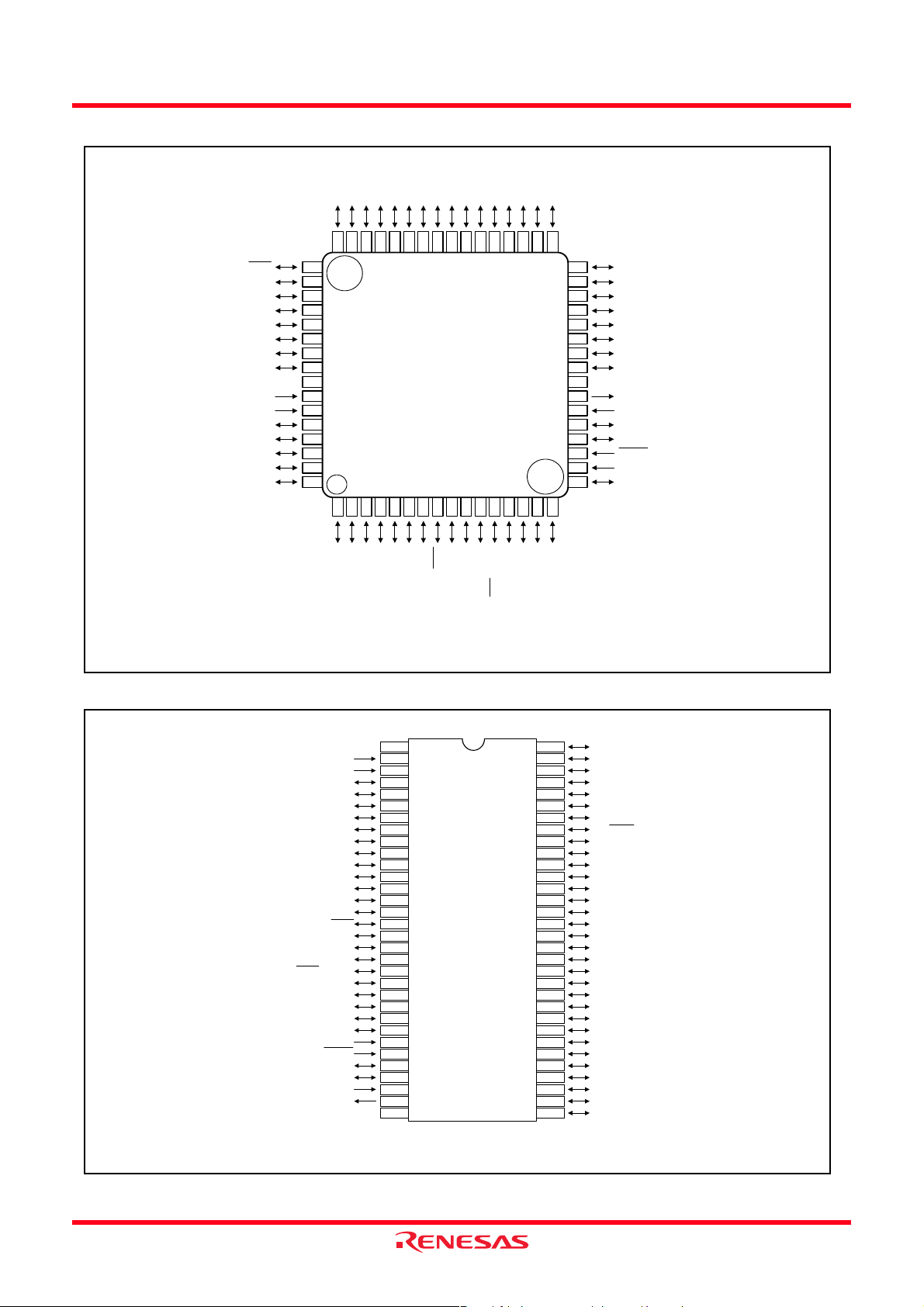
Package code : PLQP0064KB-A (64P6Q-A)/PLQP0064GA-A (64P6U-A)
Fig 1. Pin configuration (Top view) PLQP0064KB-A (64P6Q-A)/PLQP0064GA-A (64P6U-A)
VREF
AVSS
P67/AN7
P66/AN6
P65/AN5
P64/AN4
P63/AN3
P62/AN2
P61/AN1
P60/AN0
P57/INT3
P56/PWM
5/CNTR1
P5
P54/CNTR0
P53/SRDY2
P52/SCLK2
P51/SOUT2
P50/SIN2
P47/SRDY1/CNTR2
P46/SCLK1
P45/TXD1
P44/RXD1
P43/INT2
P42/INT1
CNVSS
RESET
P4
1/INT00/XCIN
P40/INT40/XCOUT
XOUT
VCC
XIN
VSS
2
3
4
5
6
7
8
9
10
11
12
13
14
15
16
17
18
19
20
21
22
23
24
25
26
27
28
29
30
31
32
M38039MFL-XXXSP
M38039FFLSP
641
63
62
61
60
59
58
57
56
55
54
53
52
51
50
49
48
47
46
45
44
43
42
41
40
39
38
37
36
35
34
33
P30/DA1
P31/DA2
P32
P33
P34/RXD3
P35/TXD3
P36/SCLK3
P37/SRDY3
P00/AN8
P01/AN9
P02/AN10
P03/AN11
P04/AN12
P05/AN13
P06/AN14
P07/AN15
P10/INT41
P11/INT01
P1
2
P13
P14
P15
P16
P17
P20(LED0)
1(LED1)
P2
P2
2(LED2)
P23(LED3)
P2
4(LED4)
P2
5(LED5)
P2
6(LED6)
P27(LED7)
Package code : PRDP0064BA-A (64P4B)
Fig 2. Pin configuration (Top view) (PRDP0064BA-A (64P4B))
Rev.1.00 Apr 2, 2007 Page 2 of 117
REJ03B0212-0100
3803 Group (Spec.L)
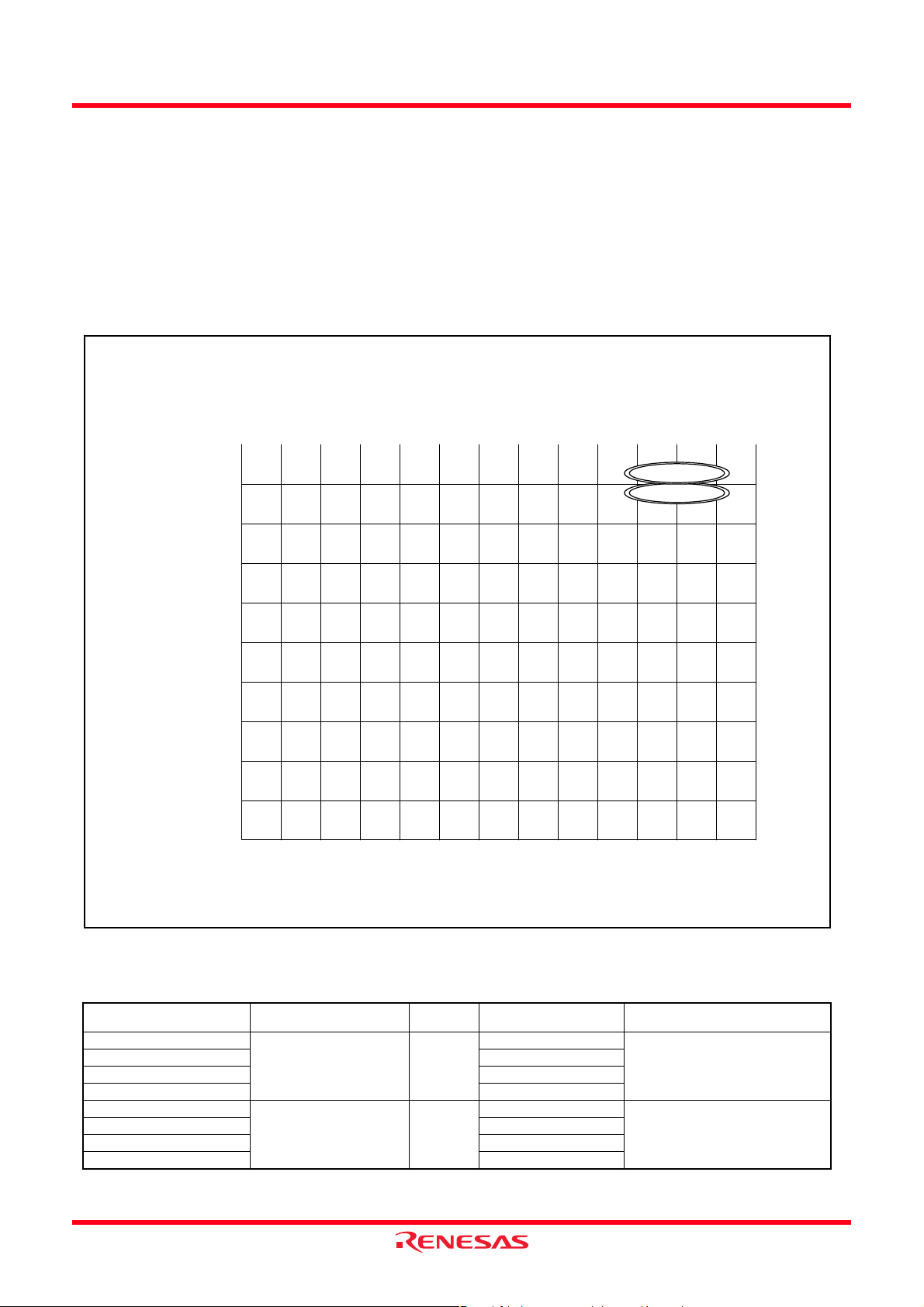
PIN CONFIGURATION (TOP VIEW)
ABCDEFGH
8
7
6
5
4
3
2
50 46 44 41 40 32 31 30
P3
6/SCLK3 P02/AN10 P04/AN12 P07/AN15 P10/INT41 P20(LED0)P21(LED1)P22(LED2)
51 47 45 42 39 27 29 28
P3
5/TXD3 P01/AN9 P03/AN11 P06/AN14 P11/INT01 P25(LED5)P23(LED3)P24(LED4)
53 52 48 43 38 37 26 25
P33 P34/RXD3 P00/AN8 P05/AN13 P12 P13 P26(LED6)P27(LED7)
56 55 54 49 33 36 35 34
P30/DA1 P31/DA2 P32 P37/SRDY3 P17 P14 P15 P16
1 64 58 59 57 24 22 23
2/AN2 P63/AN3 VREF AVSS VCC VSS XIN XOUT
P6
60 61 4 7 12 14 21 20
P67/AN7 P66/AN6 P57/INT3 P54/CNTR0
P4
7/SRDY1/CNTR2
P45/TXD1
P4
62 63 5 8 10 13 17 19
P65/AN5 P64/AN4 P56/PWM P53/SRDY2 P51/SOUT2 P46/SCLK1 P42/INT1 RESET
0/INT40/XCOUT
8
7
6
5
4
3
P41/INT00/XCIN
2
1
2 3 6 9 11 15 16 18
P61/AN1 P60/AN0 P55/CNTR1 P52/SCLK2 P50/SIN2 P44/RXD1 P43/INT2 CNVSS
ABCDEFGH
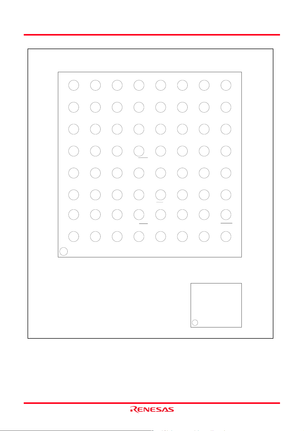
Package code : PTLG0064JA-A (64F0G)
Note : The numbers in circles corresponds with the number on the packages FP/HP/KP.
Fig 3. Pin configuration (Top view) (PTLG0064JA-A (64F0G))
1
M38039MFL
-XXXWG
M38039
FFLWG
Package (TOP VIEW)
Rev.1.00 Apr 2, 2007 Page 3 of 117
REJ03B0212-0100
3803 Group (Spec.L)
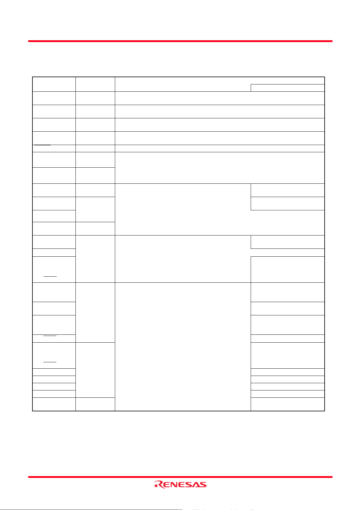
Table 1 Performance overview
Parameter Function
Number of basic instructions 71
Minimum instruction execution time 0.24 µs (Oscillation frequency 16.8 MHz)
Oscillation frequency Oscillation frequency 16.8 MHz(Maximum)
Memory
sizes
I/O port P0-P6 56 pins
Software pull-up resistors Built-in
Interrupt 21 sources, 16 vectors (8 external, 12 internal, 1 software)
Timer 8-bit × 4 (with 8-bit prescaler), 16-bit × 1
Serial interface 8-bit × 2 (UART or Clock-synchronized)
PWM 8-bit × 1 (with 8-bit prescaler)
A/D converter 10-bit × 16 channels (8-bit reading enabled)
D/A converter 8-bit × 2 channels
Watchdog timer 16-bit × 1
LED direct drive port
Clock generating circuits Built-in 2 circuits
Power
source
voltage
Power
dissipation
Input/Output
characteristics
Operating temperature range -20 to 85 °C
Device structure CMOS sillicon gate
Package 64-pin plastic molded SDIP/LQFP/FLGA
Mask ROM version ROM 60 Kbytes
RAM 2048 bytes
Flash memory version ROM 60 Kbytes
RAM 2048 bytes
8-bit × 1 (Clock-synchronized)
8 (average current: 15 mA, peak current: 30 mA, total current: 90 mA)
(connect to external ceramic rasonator or quartz-crystal oscillator)
In high-speed
mode
In middlespeed mode
In low-speed
mode
In high-speed mode Mask ROM version 40 mW
In low-speed mode Mask ROM version 45 µW
Input/Output withstand voltage VCC
Output current 10 mA
At 16.8 MHz
At 12.5 MHz
At 8.4 MHz
At 4.2 MHz Mask ROM version 2.2 to 5.5 V
At 2.1 MHz Mask ROM version 2.0 to 5.5 V
At 16.8 MHz
At 12.5 MHz
At 8.4 MHz Mask ROM version 2.2 to 5.5 V
At 6.3 MHz Mask ROM version 1.8 to 5.5 V
At 32 MHz
Mask ROM version
Flash memory version
Mask ROM version
Flash memory version
Mask ROM version
Flash memory version
Mask ROM version
Flash memory version
Mask ROM version
Flash memory version
Mask ROM version 1.8 to 5.5 V
Flash memory version 2.7 to 5.5 V
Flash memory version 27.5 mW
Flash memory version 1200 µW
4.5 to 5.5 V
4.0 to 5.5 V
2.7 to 5.5 V
4.5 to 5.5 V
2.7 to 5.5 V
Rev.1.00 Apr 2, 2007 Page 4 of 117
REJ03B0212-0100
3803 Group (Spec.L)
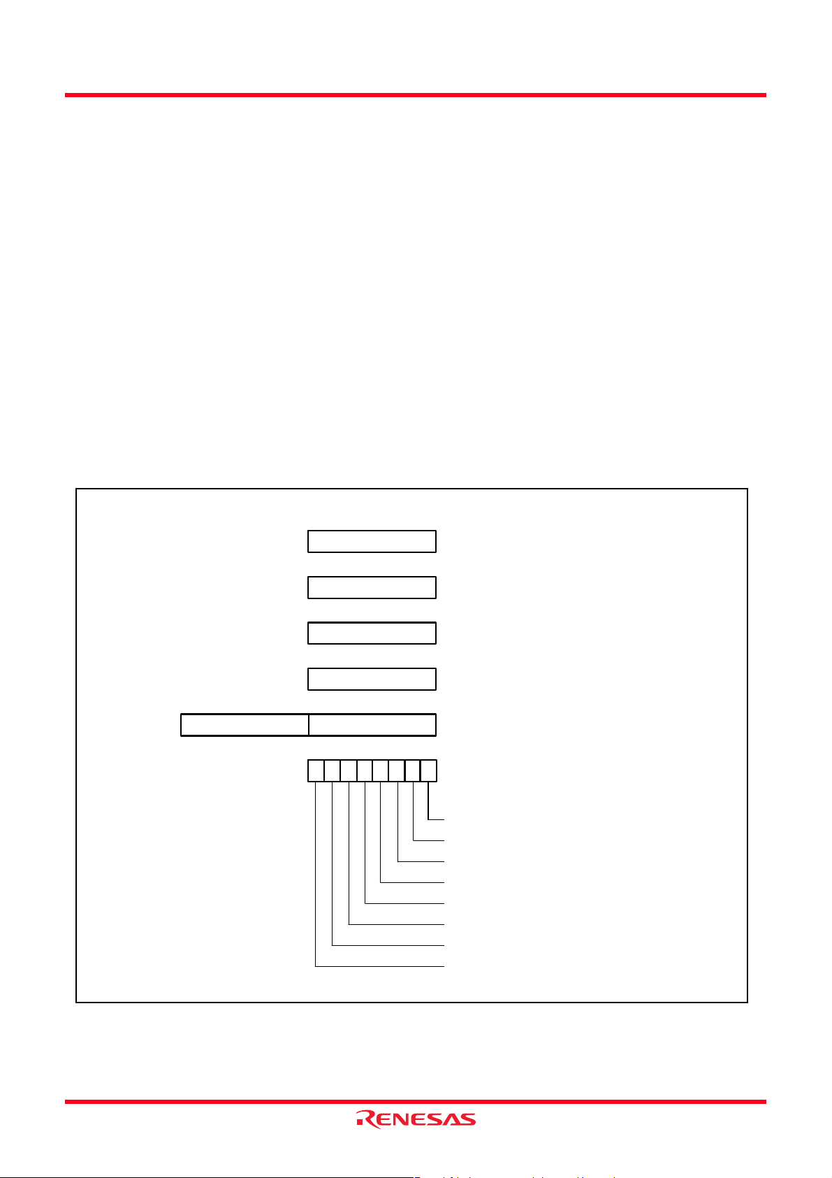
Reset in p ut
26
CNVSS
27
RESET
1
VCC
32
VSS
P0 (8)
Timer 1 (8 )
Timer 2 (8 )
Timer Y (8)
Timer X (8 )
INT01
INT41
Timer Z (16)
P1 (8)
Prescaler Y (8)
Prescaler X (8)
Prescaler 12 (8)
CNTR0
CNTR1
CNTR2
SI/O3 (8)
P2 (8)
P3 (8)
D/A
1 (8)
converter
A
X
Y
S
PS
PCLPCH
Data bus
D/A
2 (8)
converter
INT00
INT1
INT2
INT40
I/O port P0
49 50 51 52 5354 55 56
44 46 48
43 45 47
I/O port P1
42
41
I/O port P2
(LED drive)
33 35 37 3934 36 38 40
I/O port P3
58 6259 61 6360 6457
C P U
0
P4 (8)
I/O port P4
21 2522 24 2823 2920
R A M R O M
29
Sub-clock
output
28
XCIN XCOUT
Sub-clock
input
31
Main
clock
output
30
XIN XOUT
Main
clock
input
Clock generating circuit
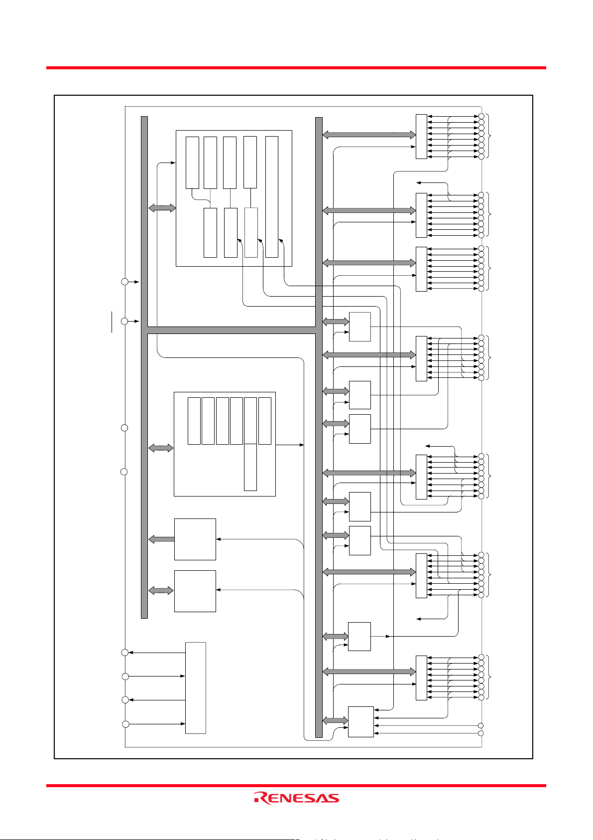
FUNCTIONAL BLOCK DIAGRAM (Package: PRDP0064BA-A (64P4B))
Fig 4. Functional block diagram
Rev.1.00 Apr 2, 2007 Page 5 of 117
REJ03B0212-0100
SI/O2 (8) SI/O1 (8)
P5 (8)
INT3
PWM (8)
P6 (8)
A/D
(10)
converter
1912
13 1714 16 1815
4681057911
3
2
I/O port P5
I/O port P6
AVSS
VREF
3803 Group (Spec.L)
PIN DESCRIPTION
Table 2 P in des c r iption
Pin Name Functions
CC, VSS Power source • Apply voltage of 1.8 V − 5.5 V to VCC, and 0 V to VSS. In the flash memory version, apply
V
SS CNVSS input • This pin controls the operation mode of the chip.
CNV
REF Reference
V
voltage of 2.7 V − 5.5 V to V
• Normally connected to V
CC.
SS.
• Reference voltage input pin for A/D and D/A converters.
Function except a port function
voltage
SS Analog power
AV
source
RESET
IN Main clock input • Input and output pins for the clock generating circuit.
X
OUT Main clock
X
Reset input • Reset input pin for active “L”.
output
P0
P0
P1
0/AN8−
7/AN15
0/INT41
I/O port P0 • 8-bit CMOS I/O port.
I/O port P1 • Interrupt input pin
P11/INT01
2−P17
P1
P20(LED0)P2
7(LED7)
0/DA1
P3
I/O port P2
I/O port P3 • 8-bit CMOS I/O port.
P31/DA2
P3
2, P33
P34/RXD3
P35/TXD3
P36/SCLK3
P37/SRDY3
0/INT40/XCOUT
P4
I/O port P4 • 8-bit CMOS I/O port.
P41/INT00/XCIN
P4
2/INT1
P43/INT2
4/RXD1
P4
• Analog power source input pin for A/D and D/A converters.
• Connect to V
SS.
• Connect a ceramic resonator or quartz-crystal oscillator between the X
the oscillation frequency.
• When an external clock is used, connect the clock source to the X
IN pin and leave the XOUT pin
open.
• A/D converter input pin
• I/O direction register allows each pin to be individually
programmed as either input or output.
• CMOS compatible input level.
• CMOS 3-state output structure.
• Pull-up control is enabled in a bit unit.
•P2
0 − P27 (8 bits) are enabled to output large current for
LED drive.
• D/A converter input pin
• I/O direction register allows each pin to be individually
programmed as either input or output.
• CMOS compatible input level.
•P3
0, P31, P34 − P37 are CMOS 3-state output structure.
•P3
2, P33 are N-channel open-drain output structure.
• Pull-up control of P3
0, P31, P34 − P37 is enabled in a bit unit.
• Serial I/O3 function pin
• Interrupt input pin
• I/O direction register allows each pin to be individually
programmed as either input or output.
• CMOS compatible input level.
• Sub-clock generating I/O pin
(resonator connected)
• Interrupt input pin
• CMOS 3-state output structure.
• Pull-up control is enabled in a bit unit.
• Serial I/O1 function pin
IN and XOUT pins to set
P45/TXD1
P46/SCLK1
P4
7/SRDY1/CNTR2
0/SIN2
P5
I/O port P5 • Serial I/O2 function pin
• Serial I/O1, timer Z function pin
P51/SOUT2
P52/SCLK2
P53/SRDY2
4/CNTR0 • Timer X function pin
P5
5/CNTR1 • Timer Y function pin
P5
6/PWM • PWM output pin
P5
7/INT3 • Interrupt input pin
P5
P6
P6
0/AN0−
7/AN7
I/O port P6 • A/D converter input pin
Rev.1.00 Apr 2, 2007 Page 6 of 117
REJ03B0212-0100

3803 Group (Spec.L)
PART NUMBERING
Product name
M3803 9 M F
−
L
XXX SP
Package code
SP : PRDP0064BA-A (64P4B)
HP : PLQP0064KB-A (64P6Q-A)
KP : PLQP0064GA-A (64P6U-A)
WG : PTLG0064JA-A (64F0G)
ROM number
Omitted in the flash memory version.
−: standard
Omitted in the flash memory version.
−: Minner spec. change product
L
ROM/Flash memory size
1: 4096 bytes
2: 8192 bytes
3: 12288 bytes
4: 16384 bytes
5: 20480 bytes
6: 24576 bytes
7: 28672 bytes
8: 32768 bytes
The first 128 bytes and the last 2 bytes of ROM are reserved areas ; they
cannot be used as a user’s ROM area.
However, they can be programmed or erased in the flash memory version,
so that the users can use them.
9: 36864 bytes
A: 40960 bytes
B: 45056 bytes
C: 49152 bytes
D: 53248 bytes
E: 57344 bytes
F: 61440 bytes
Fig 5. Part numbering
Memory type
M:Mask ROM version
F: Flash memory version
RAM size
0: 192 bytes
1: 256 bytes
2: 384 bytes
3: 512 bytes
4: 640 bytes
5: 768 bytes
6: 896 bytes
7: 1024 bytes
8: 1536 bytes
9: 2048 bytes
Rev.1.00 Apr 2, 2007 Page 7 of 117
REJ03B0212-0100
3803 Group (Spec.L)
GROUP EXPANSION
Renesas plans to expand the 3803 group (Spec.L) as follows.
Memory Size
• Flash memory size .....................................................60 Kbytes
• Mask ROM size.........................................................60 Kbytes
• RAM size................................................................. 2048 bytes
Memory Expansion Plan
ROM size (bytes)
60 K
48 K
32 K
Packages
• PRDP0064BA-A (64P4B)
..............................................64-pin shrink plastic-molded DIP
• PLQP0064KB-A (64P6Q-A)
...........................................0.5 mm-pitch plast ic molded LQFP
• PLQP0064GA-A (64P6U-A)
...........................................0.8 mm-pitch plast ic molded LQFP
• PTLG0064JA-A (64F0G)
........................................0.65 mm-pitch plastic molded FLGA
M38039FFL
M38039MFL
28 K
24 K
20 K
16 K
12 K
8 K
512
384 768640
1024896 12801152 1408 20481536
RAM size (byte s)
Fig 6. Memory expansion plan
Table 3 S up port products
Part No.
M38039MFL-XXXSP
M38039MFL-XXXHP PLQP0064KB-A (64P6Q-A)
M38039MFL-XXXKP PLQP0064GA-A (64P6U-A)
M38039MFL-XXXWG PTLG0064JA-A (64F0G)
M38039FFLSP
M38039FFLHP PLQP0064KB-A (64P6Q-A)
M38039FFLKP PLQP0064GA-A (64P6U-A)
M38039FFLWG PTLG0064JA-A (64F0G)
ROM size (bytes)
ROM size for User in ( )
61440
(61310)
57344+4096 (NOTE) 2048
RAM size
(bytes)
2048
Package Remarks
PRDP0064BA-A (64P4B)
PRDP0064BA-A (64P4B)
NOTE:
1. ROM size includes the ID code area.
Mask ROM version
Flash memory version
VCC = 2.7 to 5.5 V
40323072
Rev.1.00 Apr 2, 2007 Page 8 of 117
REJ03B0212-0100
3803 Group (Spec.L)
FUNCTIONAL DESCRIPTION
CENTRAL PROCESSING UNIT (CPU)
The 3803 group (Spec.L) uses the standard 740 Family
instruction set. Refer to the table of 740 Family addressing
modes and machine instructions or the 740 Family Software
Manual for details on the instruction set.
Machine-resident 740 Family instructions are as follows:
The FST and SLW instructions cannot be used.
The STP, WIT, MUL, and DIV instructions can be used.
[Accumulator (A)]
The accumulator is an 8-bit register. Data operations such as data
transfer, etc. are executed mainly through the accumulator.
[Index Register X (X)]
The index register X is an 8-bit register. In the index addressing
modes, the value of the OPERAND is added to the contents of
register X and specifies the real address.
[Index Register Y (Y)]
The index register Y is an 8-bit register. In partial instruction, the
value of the OPERAND is added to the contents of register Y
and specifies the real address.
b7 b0
A
b7 b0
X
b7 b0
Y
b7 b0
S
[Stack Pointer (S)]
The stack pointer is an 8-bit register used during subroutine calls
and interrupts. This register indicates start address of stored area
(stack) for storing registers during subroutine calls and
interrupts.
The low-order 8 bits of the stack address are determined by the
contents of the stack pointer. The high-order 8 bits of the stack
address are determined by the stack page selection bit. If the
stack page selection bit is “0”, the high-order 8 bits becomes
“00
16”. If the stack page selection bit is “1”, the high-order 8 bits
becomes “01
The operations of pushing register contents onto the stack and
popping them from the stack are shown in Figure 8.
Store registers other than those described in Fi gure 7 with
program when the user needs them during interrupts or
subroutine calls (see Table 4).
[Program Counter (PC)]
The program counter is a 16-bit counter consisting of two 8-bit
registers PC
next instruction to be executed.
16”.
H and PCL. It is used to indicate the address of the
Accumulator
Index Register X
Index Register Y
Stack Pointer
b15
b7 b0
b7 b0
Fig 7. 740 Family CPU register structure
PC
LPCH
Program Counter
CZIDBTVN
Processor Status Register (PS)
Carry Flag
Zero Flag
Interrupt Disable Flag
Decimal Mode Flag
Break Flag
Index X Mode Flag
Overflow Flag
Negative Flag
Rev.1.00 Apr 2, 2007 Page 9 of 117
REJ03B0212-0100
3803 Group (Spec.L)
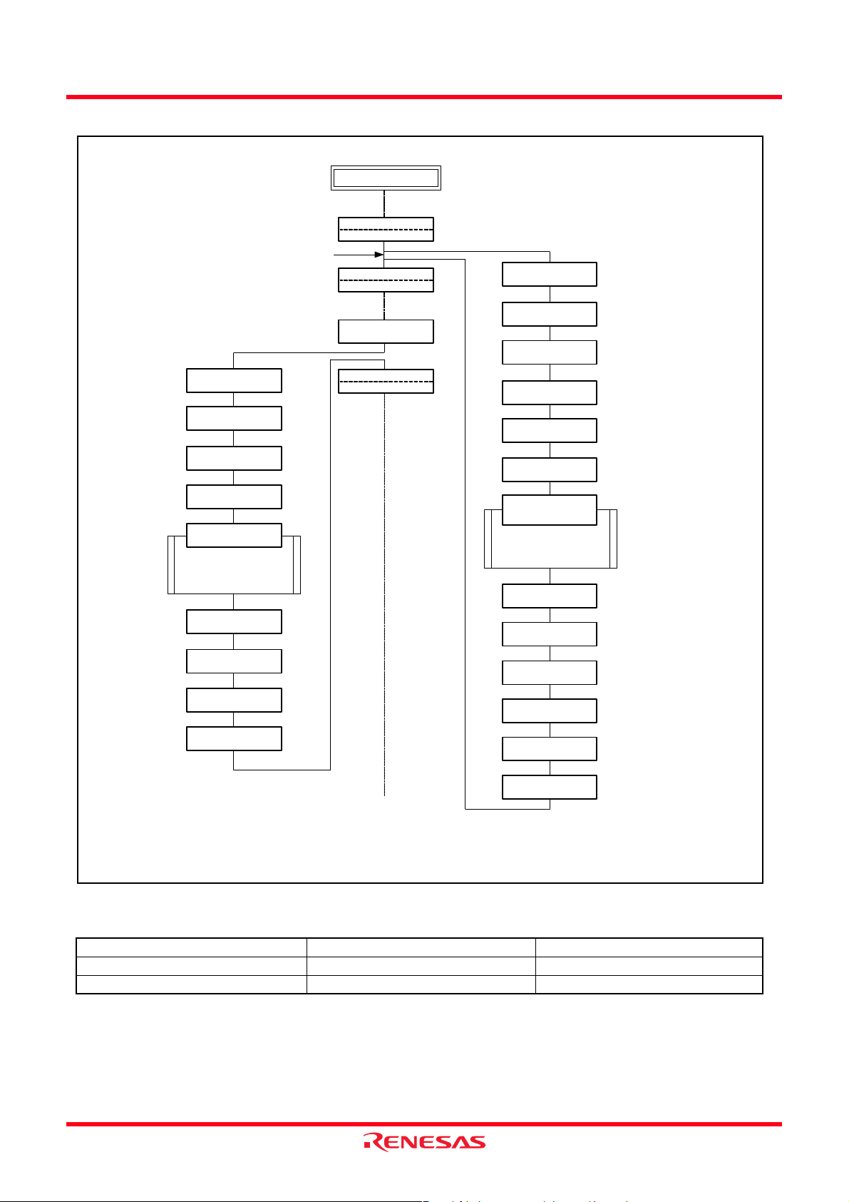
On-going Routine
Push Return
Address
on Stack
POP Return
Address from
Stack
Interrupt request
M(S)←(PCH)
(S)←(S) − 1
M(S)←(PCL)
(S)←(S) − 1
Subroutine
.....
Execute RTS
(S)←(S) + 1
(PCL)←M(S)
(1)
Execute JSR
M(S)←(PCH)
(S)←(S) − 1
M(S)←(PCL)
(S)←(S) − 1
M(S)←(PS)
(S)←(S) − 1
Interrupt
Service Routine
.....
Execute RTI
(S)←(S) + 1
(PS)←M(S)
(S)←(S) + 1
Push Return Address
on Stack
Push Contents of
Processor
Status Register on Stack
I Flag is Set from
“0” to “1”
Fetch the Jump
Vector
POP Contents of
Processor Status Register
from Stack
(S)←(S) + 1
(PCH)←M(S)
Note 1 : Condition for acceptance of an interrupt → Interrupt enable flag is “1”
Interrupt disable flag is “0”
(PCL)←M(S)
(S)←(S) + 1
(PCH)←M(S)
POP Return
Address from Stack
Fig 8. Register push and pop at interrupt generatio n and subroutine call
Table 4 Push and pop instructions of accumulator or processor status register
Push instruction to stack Pop instruction from stack
Accumulator PHA PLA
Processor status register PHP PLP
Rev.1.00 Apr 2, 2007 Page 10 of 117
REJ03B0212-0100

3803 Group (Spec.L)
[Processor status register (PS)]
The processor status register is an 8-bit register consisting of 5
flags which indicate the status of the processor after an
arithmetic operation and 3 flags which decide MCU operation.
Branch operations can be performed by testing the Carry (C)
flag, Zero (Z) flag, Overflow (V) flag, or the Negative (N) flag.
In decimal mode, the Z, V, N flags are not valid.
Bit 0: Carry flag (C)
The C flag contains a carry or borrow generated by the
arithmetic logic unit (ALU) immediately after an arithmetic
operation. It can also be changed by a sh ift or rotate
instruction.
Bit 1: Zero flag (Z)
The Z flag is set if the result of an immediate arithmetic
operation or a data transfer is “0”, and cleared if the result is
anything other than “0”.
Bit 2: Interrupt disable flag (I)
The I flag disables all interrupts except for the interrupt
generated by the BRK instruction.
Interrupts are disabled when the I flag is “1”.
Bit 3: Decimal mode flag (D)
The D flag determines whether additions and subtractions are
executed in binary or decimal. Binary arithmetic is executed
when this flag is “0”; decimal arithmetic is executed when it
is “1”.
Decimal correction is automatic in decimal mode. Only the
ADC and SBC instructions can execute decimal arithmetic.
Bit 4: Break flag (B)
The B flag is used to indicate that the current interrupt was
generated by the BRK instruction. The BRK flag in the
processor status register is always “0”. When the BRK
instruction is used to generate an interrupt, the processor
status register is pushed onto the stack with the break flag set
to “1”.
Bit 5: Index X mode flag (T)
When the T flag is “0”, arithmetic operations are performed
between accumulator and memory. When the T flag is “1”,
direct arithmetic operations and direct data transfers are
enabled between memory locations.
Bit 6: Overflow flag (V)
The V flag is used during the addition or subtraction of one
byte of signed data. It is set if the result exceeds +127 to −
128. When the BIT instruction is executed, bit 6 of the
memory location operated on by the BIT instruction is stored
in the overflow flag.
Bit 7: Negative flag (N)
The N flag is set if the result of an arithmetic operation or
data transfer is negative. When the BIT instruction is
executed, bit 7 of the memory location operated on by the
BIT instruction is stored in the negative flag.
Table 5 Set and clear instructions of each bit of processor status register
C flag Z flag I flag D flag B flag T flag V flag N flag
Set instruction SEC
Clear instruction CLC − CLI CLD − CLT CLV −
− SEI SED − SET −−
Rev.1.00 Apr 2, 2007 Page 11 of 117
REJ03B0212-0100
3803 Group (Spec.L)
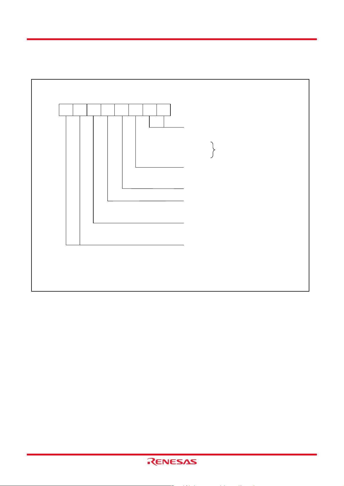
[CPU Mode Register (CPUM)] 003B16
The CPU mode register contains the stack page selection bit, the
internal system clock control bits, etc.
The CPU mode register is allocated at address 003B16.
b7 b0
1
CPU mode register
(CPUM: address 003B
Processor mode bits
b1 b0
0 0 : Single-chip mode
01:
1 0 : Not available
11:
Stack page selection bit
0 : 0 page
1 : 1 page
Fix this bit to “1”.
Port XC switch bit
0 : I/O port function (stop oscillating)
CIN-XCOUT oscillating function
1:X
Main clock (X
0 : Oscillating
1 : Stopped
Main clock division ratio selection bits
b7 b6
00:φ = f(X
01:φ = f(X
10:φ = f(X
1 1 : Not available
IN-XOUT) stop bit
16)
IN)/2 (high-speed mode)
IN)/8 (middle-speed mode)
CIN)/2 (low-speed mode)
Fig 9. Structure of CPU mode register
Rev.1.00 Apr 2, 2007 Page 12 of 117
REJ03B0212-0100
3803 Group (Spec.L)
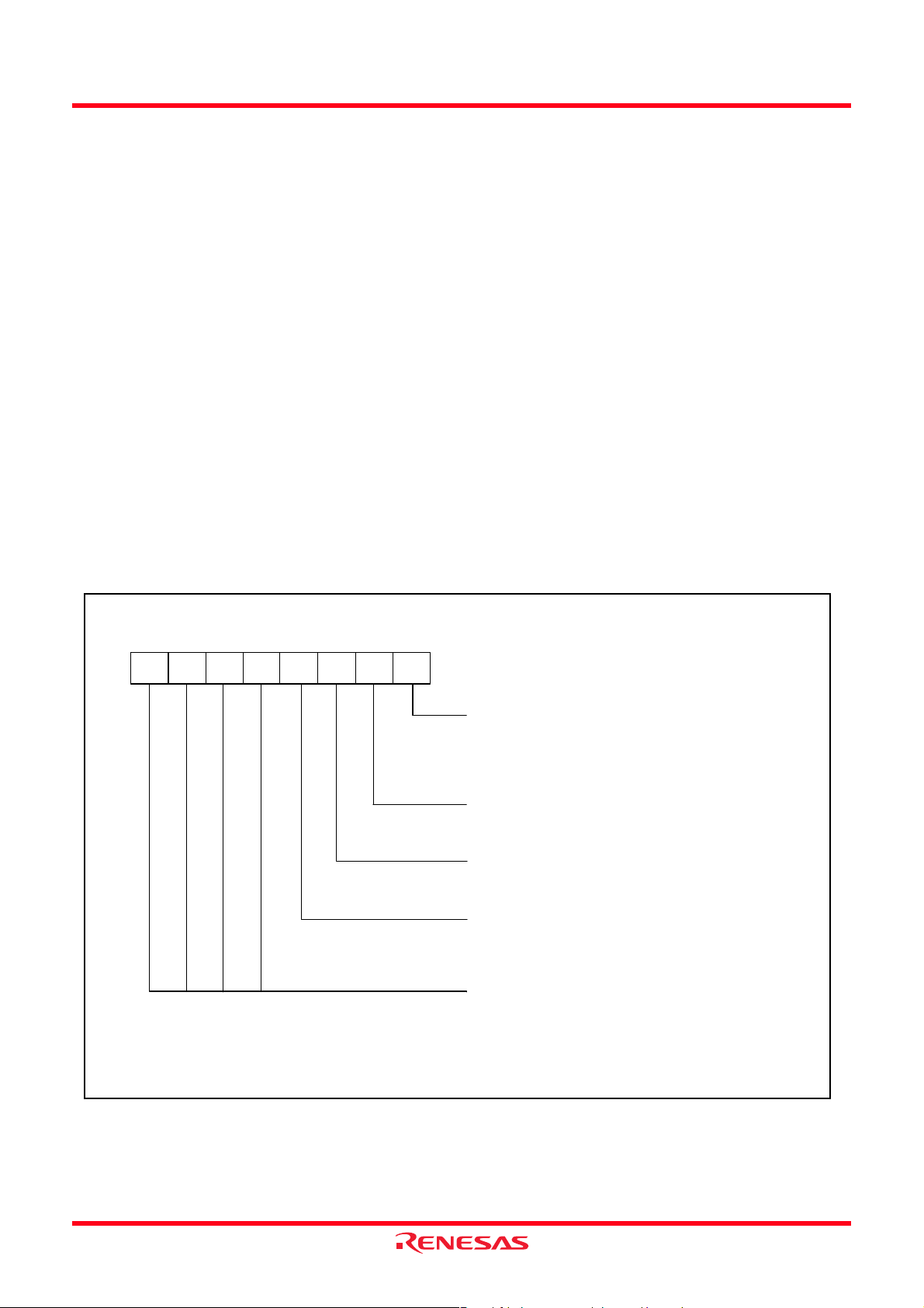
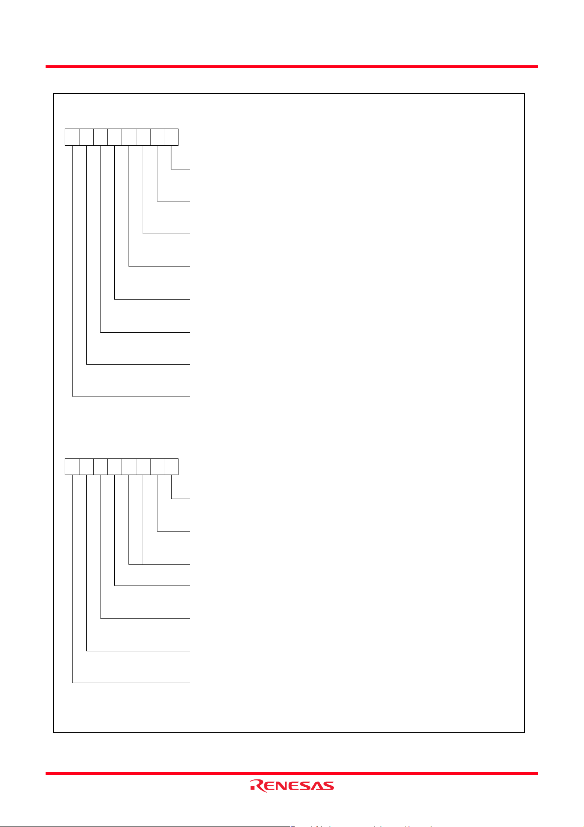
MISRG
(1) Bit 0 of address 0010
16: Oscillation stabilizing time
set after STP instruction released bit
When the MCU stops the clock oscillation by the STP instruction
and the STP instruction has been released by an external
interrupt source, usually, the fixed values of Timer 1 and
Prescaler 12 (Timer 1 = 0116, Prescaler 12 = FF16) are
automatically reloaded in order for the oscillation to stabilize.
The user can inhibit the automatic setting by setting “1” to bit 0
of MISRG (address 0010
16).
However, by setting this bit to “1”, the previous values, set just
before the STP instruction was executed, will remain in Timer 1
and Prescaler 12. Therefore, you will need to set an appropriate
value to each register, in accordance with the oscillation
stabilizing time, before executing the STP instruction.
Figure 10 shows the structure of MISRG.
(2) Bits 1, 2, 3 of address 0010
16: Middle-speed Mode
Automatic Switch Function
In order to switch the clock mode of an MCU which has a subclock, the following procedure is necessary:
set CPU mode register (003B
16) --> start main clock oscillation
--> wait for oscillation stabilization --> switch to middle-speed
mode (or high-speed mode).
However, the 3803 group (Spec.L) has the built-in function
which automatically switches from low to middle-spee d mode by
program.
• Middle-speed mode automatic switch by program
The middle-speed mode can also be automatically switche d by
program while operating in low-speed mode. By setting the
middle-speed automatic switch start bit (bit 3) of MISRG
(address 0010
16) to “1” in the condition that the middle-speed
mode automatic switch set bit is “1” while operating in lowspeed mode, the MCU will automatically switch to middle-speed
mode. In this case, the oscillation stabilizing time of the main
clock can be selected by the middle-speed automatic switch wait
time set bit (bit 2) of MISRG (address 0010
16).
b7 b0
Note 1 : When automatic switch to middle-speed mode from low-speed mode occurs,
the values of CPU mode register (3B
MISRG
(MISRG: address 0010
Oscillation stabilizing time set after STP instruction
released bit
0 : Automatically set “01
Prescaler 12
1 : Automatically set disabled
Middle-speed mode automatic switch set bit
0 : Not set automatically
1 : Au tomatic switching enabled
Middle-speed mode automatic switch wait time set bit
0 : 4.5 to 5.5 machine cycles
1 : 6.5 to 7.5 machine cycles
Middle-speed mode automatic switch start bit
(Depending on program)
0 : Invalid
1 : Automatic switch start
Not used (return “0” when read)
(Do not write “1” to this bit)
16) change.
16)
16” to Timer 1, “FF16” to
(1)
(1)
Fig 10. Structure of MISRG
Rev.1.00 Apr 2, 2007 Page 13 of 117
REJ03B0212-0100
3803 Group (Spec.L)
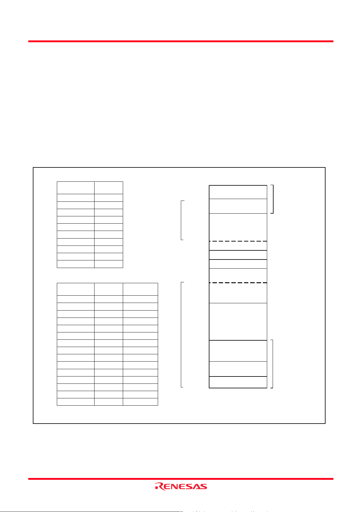
MEMORY
• Special Function Register (SFR) Area
The Special Function Register area in the zero page contains
control registers such as I/O ports and timers.
• RAM
The RAM is used for data storage and for stack area of
subroutine calls and interrupts.
•ROM
The first 128 bytes and the last 2 bytes of ROM are reserved for
device testing and the rest is a user area for storing programs.
The reserved ROM area can program/erase in the flash memory
version.
RAM area
RAM size
(bytes)
192
256
384
512
640
768
896
1024
1536
2048
Address
XXXX
00FF
16
013F16
01BF16
023F16
02BF16
033F16
03BF16
043F16
063F16
083F16
16
RAM
ROM area
ROM size
(bytes)
4096
8192
12288
16384
20480
24576
28672
32768
36864
40960
45056
49152
53248
57344
61440
Address
YYYY
F000
16
E00016
D00016
C00016
B00016
A00016
900016
800016
700016
600016
500016
400016
300016
200016
100016
Address
16
ZZZZ
16
F08016
E08016
D08016
C08016
B08016
A08016
ROM
908016
808016
708016
608016
508016
408016
308016
208016
108016
• Interrupt Vector Area
The interrupt vector area contains reset and interrupt vectors.
• Zero Page
Access to this area with only 2 bytes is possible in the zero page
addressing mode.
• Special Page
Access to this area with only 2 bytes is possible in the special
page addressing mode.
<Note>
Since the contents of RAM are undefined at reset, be sure to set
an initial value before use.
000016
004016
SFR area
Zero page
010016
XXXX16
0FE016
0FEF16
0FF016
0FFF
16
Not used
SFR area (Note 1)
SFR area
Not used
YYYY16
Reserved ROM area
(128 bytes)
ZZZZ16
FF0016
FFDC16
Special page
Interrupt vector area
FFFE16
FFFF16
Notes1: Only flash memory version has this SFR area.
2: The reserved ROM area can program/erase in
Reserved ROM area
the flash memory version. Note the difference of
the mask version.
Fig 11. Memory map diagram
Rev.1.00 Apr 2, 2007 Page 14 of 117
REJ03B0212-0100
3803 Group (Spec.L)
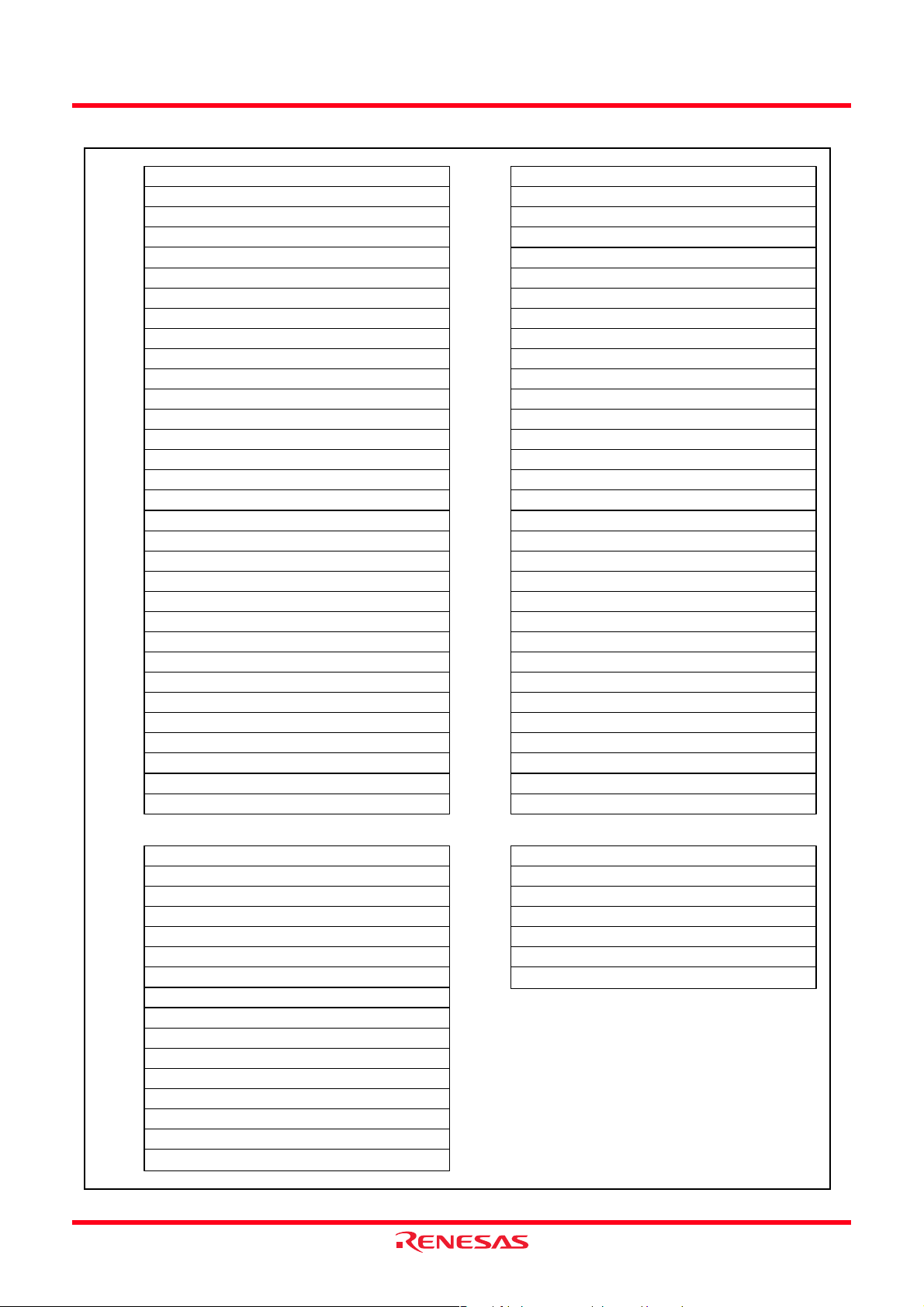
000016
000116
000216
000316
000416
000516
000616
000716
000816
000916
000A16
000B16
000C16
000D16
000E16
000F16
001016
001116
001216
001316
001416
001516
001616
001716
001816
001916
001A16
001B16
001C16
001D16
001E16
001F16
Port P0 (P0)
Port P0 direction register (P0D)
Port P1 (P1)
Port P1 direction register (P1D)
Port P2 (P2)
Port P2 direction register (P2D)
Port P3 (P3)
Port P3 direction register (P3D)
Port P4 (P4)
Port P4 direction register (P4D)
Port P5 (P5)
Port P5 direction register (P5D)
Port P6 (P6)
Port P6 direction register (P6D)
Timer 12, X count source selection register (T12XCSS)
Timer Y, Z count source selection register (TYZCSS)
MISRG
Reserved (Note 1)
Reserved (Note 1)
Reserved (Note 1)
Reserved (Note 1)
Reserved (Note 1)
Reserved (Note 1)
Reserved (Note 1)
Transmit/Receive buffer register 1 (TB1/RB1)
Serial I/O1 status register (SIO1 STS)
Serial I/O1 control register (SIO1CON)
UART1 control register (UART1CON)
Baud rate generator (BRG1)
Serial I/O2 control register (SIO2CON)
Watchdog timer control register (WDTCON)
Serial I/O2 register (SIO2)
002016
002116
002216
002316
002416
002516
002616
002716
002816
002916
002A16
002B16
002C16
002D16
002E16
002F16
003016
003116
003216
003316
003416
003516
003616
003716
003816
003916
003A16
003B16
003C16
003D16
003E16
003F16
Prescaler 12 (PRE12)
Timer 1 (T1)
Timer 2 (T2)
Timer XY mode register (TM)
Prescaler X (PREX)
Timer X (TX)
Prescaler Y (PREY)
Timer Y (TY)
Timer Z low-order (TZL)
Timer Z high-order (TZH)
Timer Z mode register (TZM)
PWM control register (PWMCON)
PWM prescaler (PREPWM)
PWM register (PWM)
Baud rate generator 3 (BRG3)
Transmit/Receive buffer register 3 (TB3/RB3)
Serial I/O3 status register (SIO3STS)
Serial I/O3 control regist er (SIO3CON)
UART3 control register (UART3CON)
AD/DA control register (ADCON)
AD conversion register 1 (AD1)
DA1 conversion register (DA1)
DA2 conversion register (DA2)
AD conversion register 2 (AD2)
Interrupt source selection register (INTSEL)
Interrupt edge selection register (INTEDGE)
CPU mode register (CPUM)
Interrupt request register 1 (IREQ1)
Interrupt request register 2 (IREQ2)
Interrupt control register 1 (ICON1)
Interrupt control register 2 (ICON2)
0FE016
0FE116
0FE216
0FE316
0FE416
0FE516
0FE616
0FE716
0FE816
0FE916
0FEA16
0FEB16
0FEC16
0FED16
0FEE16
0FEF16
Flash memory control register 0 (FMCR0)
Flash memory control register 1 (FMCR1)
Flash memory control register 2 (FMCR2)
Reserved (Note 1)
Reserved (Note 1)
Reserved (Note 1)
Reserved (Note 1)
Reserved (Note 1)
Reserved (Note 1)
Reserved (Note 1)
Reserved (Note 1)
Reserved (Note 1)
Reserved (Note 1)
Reserved (Note 1)
Reserved (Note 1)
Reserved (Note 1)
Fig 12. Memory map of special function register (SFR)
Rev.1.00 Apr 2, 2007 Page 15 of 117
REJ03B0212-0100
0FF016
0FF116
0FF216
0FF316
0FF416
0FF516
0FF616
Notes1: Do not write any data to these addresses, because these are
Port P0 pull-up control register (PULL0)
Port P1 pull-up control register (PULL1)
Port P2 pull-up control register (PULL2)
Port P3 pull-up control register (PULL3)
Port P4 pull-up control register (PULL4)
Port P5 pull-up control register (PULL5)
Port P6 pull-up control register (PULL6)
reserved area.
2: Do not access to the SFR area including nothing.
3803 Group (Spec.L)
I/O PORTS
The I/O ports have direction registers which determine the
input/output direction of each individual pin. Each bit in a
direction register corresponds to one pin, and each pin can be set
to be input port or output port.
When “0” is written to the bit corresponding to a pin, that pin
input are floating. If a pin set to input is written to, only the port
output latch is written to and the pin remains floating.
By setting the port P0 pull-up control register (address 0FF016)
to the port P6 pull-up control register (address 0FF6
16) ports can
control pull-up with a program. However, the contents of these
registers do not affect ports programmed as the output ports.
becomes an input pin. When “1” is written to that bit, that pin
becomes an output pin.
If data is read from a pin which is set to output, the value of the
port output latch is read, not the value of the pin itself. Pins set to
Table 6 I /O po rt function
Pin Name Input/
Output
0/AN8−P07/AN15 Port P0 Input/output,
P0
P10/INT
41
P11/INT
01
2−P17 (3)
P1
0(LED0)−
P2
7(LED7)
P2
0/DA1
P3
Port P1 External interrupt input Interrupt edge selection register (2)
Port P2
Port P3 D/A converter output AD/DA control register (4)
individual
bits
P31/DA2
2, P33 CMOS compatible
P3
P3
4/RXD3
P35/TXD3
P36/SCLK3
P37/SRDY3
P4
0/INT40/XCOUT
Port P4 External interrupt input
P41/INT00/XCIN
2/INT1
P4
P43/INT2
4/RXD1
P4
P45/TXD1
P46/SCLK1
P4
7/SRDY1/CNTR2
P5
0/SIN2
Port P5 Serial I/O2 function I/O Serial I/O2 control register (13)
P51/SOUT2
P52/SCLK2
P53/SRDY2
P5
4/CNTR0
P5
5/CNTR1
6/PWM PWM output PWM control register (18)
P5
7/INT3 External interrupt input Interrupt edge selection register (2)
P5
0/AN0−P67/AN7 Port P6 A/D converter input AD/DA control register (1)
P6
I/O Structure Non-Port Function Related SFRs Ref.
CMOS compatible
A/D converter input AD/DA control register (1)
input level
CMOS 3-state
output
input level
N-channel
open-drain output
CMOS compatible
input level
Serial I/O3 function I/O Serial I/O3 control register
UART3 control register
CMOS 3-state
output
Interrupt edge selection register
Sub-clock generating circuit
CPU mode register
External interrupt input Interrupt edge selection register (2)
Serial I/O1 function I/O Serial I/O1 control register
UART1 control register
Serial I/O1 function I/O
Timer Z function I/O
Serial I/O1 control register
Timer Z mode register
Timer X, Y function I/O Timer XY mode register (17)
NOTES:
1. Refer to the applicable sections how to use double-function ports as function I/O ports.
2. Make sure that the input level at each pin is either 0 V or VCC during execution of the STP instruction.
When an input level is at an intermediate potential, a current will flow from V
CC to VSS through the input-stage gate.
No.
(5)
(6)
(7)
(8)
(9)
(10)
(11)
(6)
(7)
(8)
(12)
(14)
(15)
(16)
Rev.1.00 Apr 2, 2007 Page 16 of 117
REJ03B0212-0100
3803 Group (Spec.L)
(1) Ports P0, P6
Data bus
(3) Ports P12 to P17, P2
Data bus
Pull-up control bit
Direction
register
Port latch
A/D converter input
Pull-up control bit
Direction
register
Port latch
Analog input pin
selection bit
(2) Ports P10, P11, P42, P43, P57
Pull-up control bit
Direction
register
Data bus
Port latch
(4) Ports P30, P31
Pull-up control bit
Direction
register
Data bus
Port latch
D/A converter output
Interrupt input
DA1 output enable bit (P30)
2 output enable bit (P31)
DA
(5) Ports P32, P33
Data bus
(7) Ports P35, P45
Serial I/O enable bit
Transmit enable bit
Direction
register
Data bus
Port latch
Serial I/O output
Direction
register
Port latch
Pull-up control bit
P-channel
output
disable bit
(6) Ports P34, P44
Serial I/O enable bit
Receive enable bit
Data bus
(8) Ports P36, P46
Serial I/O synchronous clock
Serial I/O mode selection bit
selection bit
Serial I/O enable bit
Serial I/O enable bit
Data bus
Serial I/O clock output
Pull-up control bit
Direction
register
Port latch
Direction
register
Port latch
Serial I/O external clock input
Serial I/O input
Pull-up control bit
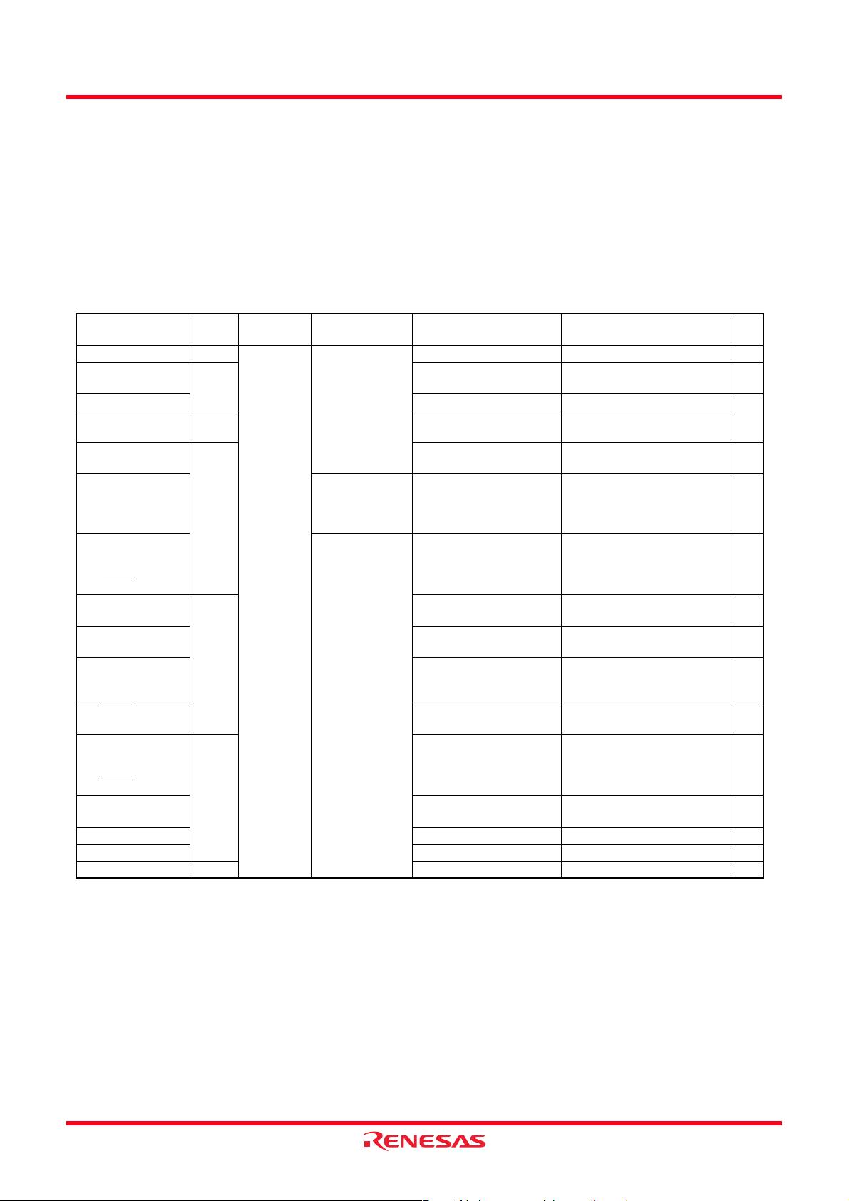
Fig 13. Port block diagram (1)
Rev.1.00 Apr 2, 2007 Page 17 of 117
REJ03B0212-0100
3803 Group (Spec.L)
(9) Port P37
Serial I/O3 mode selection bit
Serial I/O3 enable bit
SRDY3 output enable bit
Direction
register
Data bus
Serial I/O3 ready output
Port latch
(11) Port P41
Port XC switch bit
Direction
register
Data bus
Port latch
Sub-clock generating circuit input
Pull-up control bit
Pull-up control bit
INT00 Interrupt input
Port XC
switch bit
(10) Port P40
Port XC switch bit
Direction
register
Data bus
Port latch
(12) Port P47
Timer Z operating
mode bits
Bit 2
Bit 1
Bit 0
Serial I/O1 mode selection bit
Serial I/O1 enable bit
SRDY1 output enable bit
Direction
register
Data bus
Port latch
Pull-up control bit
INT40 Interrupt input
Pull-up control bit
Port XC
switch bit
(13) Port P50
Pull-up control bit
Direction
register
Data bus
Port latch
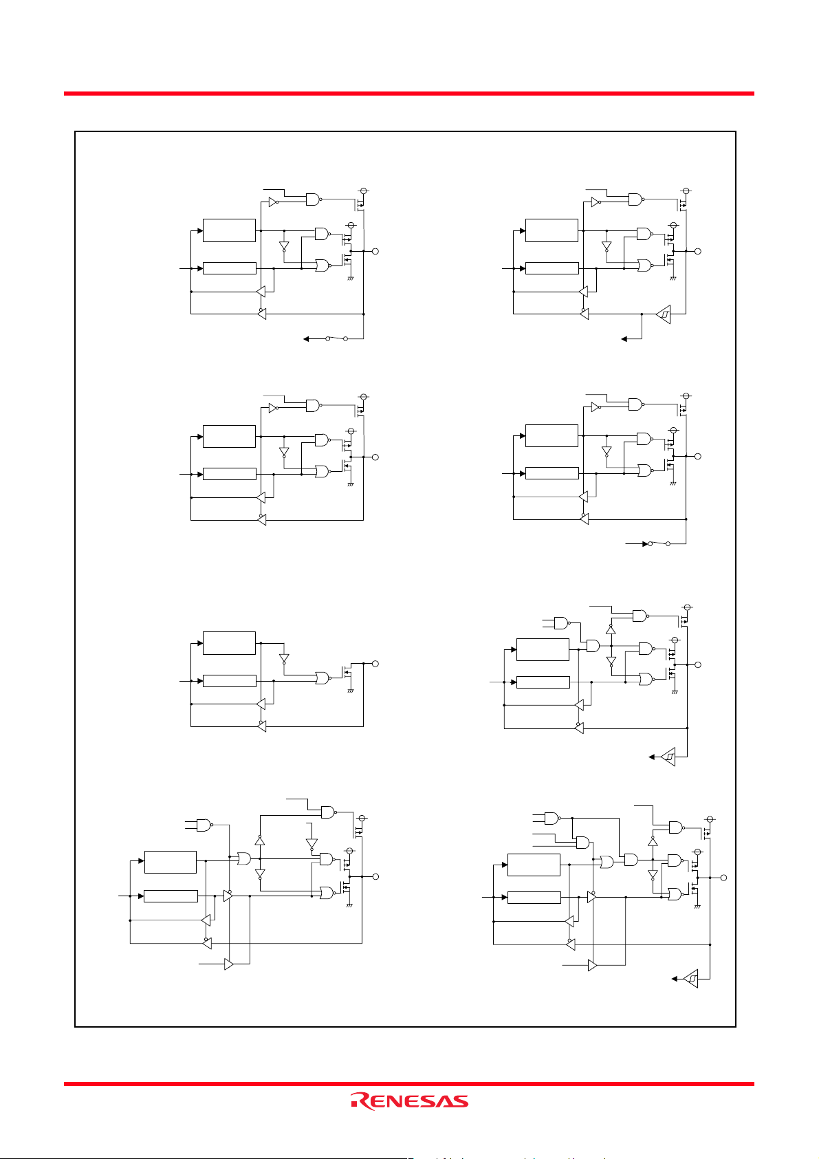
Fig 14. Port block diagram (2)
Serial I/O2 input
Timer output
Serial I/O1 ready output
(14) Port P51
Serial I/O2 transmit completion signal
Serial I/O2 port selection bit
Direction
register
Data bus
Port latch
Serial I/O2 output
2 interrupt input
CNTR
Pull-up control bit
P-channel
output
disable bit
Rev.1.00 Apr 2, 2007 Page 18 of 117
REJ03B0212-0100
3803 Group (Spec.L)
(15) Port P52
Serial I/O2 synchronous clock
Data bus
selection bit
Serial I/O2 port selection bit
Direction
register
Port latch
Serial I/O2 clock output
(17) Ports P54, P55
Direction
register
Data bus
Port latch
Pulse output mode
Timer output
Pull-up control bit
Serial I/O2 external clock input
Pull-up control bit
CNTR Interrupt input
(16) Port P53
SRDY2 output enable bit
Data bus
(18) Port P56
PWM function enable bit
Data bus
Direction
register
Port latch
Serial I/O2 ready output
Direction
register
Port latch
PWM output
Pull-up control bit
Pull-up control bit
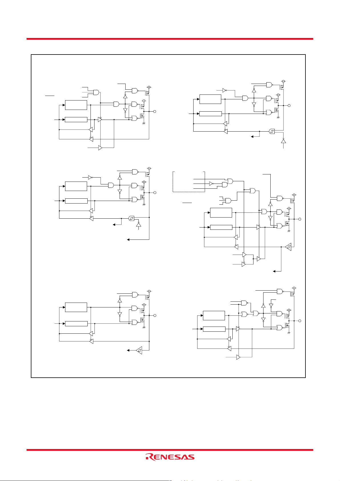
Fig 15. Port block diagram (3)
Rev.1.00 Apr 2, 2007 Page 19 of 117
REJ03B0212-0100

3803 Group (Spec.L)
b7 b0
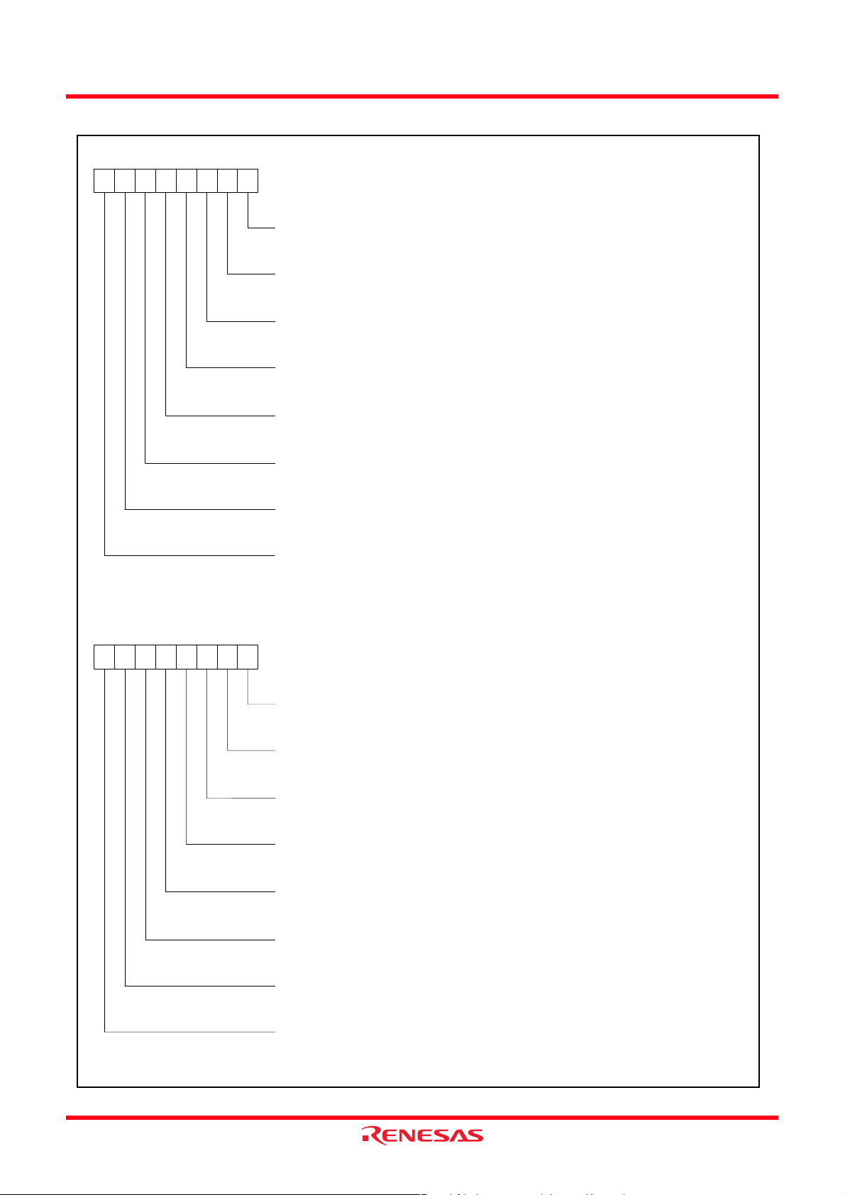
Port P0 pull-up control register
(PULL0: address 0FF0
0 pull-up control bit
P0
16)
0: No pull-up
1: Pull-up
P0
1 pull-up control bit
0: No pull-up
1: Pull-up
2 pull-up control bit
P0
0: No pull-up
1: Pull-up
P0
3 pull-up control bit
0: No pull-up
1: Pull-up
4 pull-up control bit
P0
0: No pull-up
1: Pull-up
P0
5 pull-up control bit
0: No pull-up
1: Pull-up
6 pull-up control bit
P0
0: No pull-up
1: Pull-up
7 pull-up control bit
P0
0: No pull-up
1: Pull-up
Note: Pull-up control is valid when the corresponding
bit of the port direction register is “0” (input).
When that bit is “1” (output), pull-up cannot be
set to the port of which pull-up is selected.
b7 b0
Port P1 pull-up control register
(PULL1: address 0FF1
0 pull-up control bit
P1
16)
0: No pull-up
1: Pull-up
P1
1 pull-up control bit
0: No pull-up
1: Pull-up
2 pull-up control bit
P1
0: No pull-up
1: Pull-up
P1
3 pull-up control bit
0: No pull-up
1: Pull-up
4 pull-up control bit
P1
0: No pull-up
1: Pull-up
P1
5 pull-up control bit
0: No pull-up
1: Pull-up
P1
6 pull-up control bit
0: No pull-up
1: Pull-up
7 pull-up control bit
P1
0: No pull-up
1: Pull-up
Note: Pull-up control is valid when the corresponding
bit of the port direction register is “0” (input).
When that bit is “1” (output), pull-up cann ot be
set to the port of which pull-up is selected.
Fig 16. Structure of port pull-up control register (1)
Rev.1.00 Apr 2, 2007 Page 20 of 117
REJ03B0212-0100
3803 Group (Spec.L)
b7 b0
Port P2 pull-up control register
(PULL2: address 0FF2
0 pull-up control bit
P2
16)
0: No pull-up
1: Pull-up
1 pull-up control bit
P2
0: No pull-up
1: Pull-up
P2
2 pull-up control bit
0: No pull-up
1: Pull-up
P2
3 pull-up control bit
0: No pull-up
1: Pull-up
4 pull-up control bit
P2
0: No pull-up
1: Pull-up
P2
5 pull-up control bit
0: No pull-up
1: Pull-up
6 pull-up control bit
P2
0: No pull-up
1: Pull-up
P2
7 pull-up control bit
0: No pull-up
1: Pull-up
Note: Pull-up control is valid when the corresponding
bit of the port direction register is “0” (input).
When that bit is “1” (output), pull-up cannot be
set to the port of which pull-up is selected.
b7 b0
Port P3 pull-up control register
(PULL3: address 0FF3
0 pull-up control bit
P3
16)
0: No pull-up
1: Pull-up
1 pull-up control bit
P3
0: No pull-up
1: Pull-up
Not used
(return “0” when read)
P3
4 pull-up control bit
0: No pull-up
1: Pull-up
5 pull-up control bit
P3
0: No pull-up
1: Pull-up
P3
6 pull-up control bit
0: No pull-up
1: Pull-up
7 pull-up control bit
P3
0: No pull-up
1: Pull-up
Note: Pull-up control is valid when the corresponding
bit of the port direction register is “0” (input).
When that bit is “1” (output), pull-up cann ot be
set to the port of which pull-up is selected.
Fig 17. Structure of port pull-up control register (2)
Rev.1.00 Apr 2, 2007 Page 21 of 117
REJ03B0212-0100
3803 Group (Spec.L)
b7 b0
Port P4 pull-up control register
(PULL4: address 0FF4
0 pull-up control bit
P4
16)
0: No pull-up
1: Pull-up
P4
1 pull-up control bit
0: No pull-up
1: Pull-up
2 pull-up control bit
P4
0: No pull-up
1: Pull-up
P4
3 pull-up control bit
0: No pull-up
1: Pull-up
4 pull-up control bit
P4
0: No pull-up
1: Pull-up
P4
5 pull-up control bit
0: No pull-up
1: Pull-up
6 pull-up control bit
P4
0: No pull-up
1: Pull-up
7 pull-up control bit
P4
0: No pull-up
1: Pull-up
Note: Pull-up control is valid when the corresponding
bit of the port direction register is “0” (input).
When that bit is “1” (output), pull-up cannot be
set to the port of which pull-up is selected.
b7 b0
Port P5 pull-up control register
(PULL5: address 0FF5
0 pull-up control bit
P5
16)
0: No pull-up
1: Pull-up
P5
1 pull-up control bit
0: No pull-up
1: Pull-up
2 pull-up control bit
P5
0: No pull-up
1: Pull-up
P5
3 pull-up control bit
0: No pull-up
1: Pull-up
4 pull-up control bit
P5
0: No pull-up
1: Pull-up
P5
5 pull-up control bit
0: No pull-up
1: Pull-up
P5
6 pull-up control bit
0: No pull-up
1: Pull-up
7 pull-up control bit
P5
0: No pull-up
1: Pull-up
Note: Pull-up control is valid when the corresponding
bit of the port direction register is “0” (input).
When that bit is “1” (output), pull-up cann ot be
set to the port of which pull-up is selected.
Fig 18. Structure of port pull-up control register (3)
Rev.1.00 Apr 2, 2007 Page 22 of 117
REJ03B0212-0100
3803 Group (Spec.L)
b7 b0
Port P6 pull-up control register
(PULL6: address 0FF6
0 pull-up control bit
P6
16)
0: No pull-up
1: Pull-up
1 pull-up control bit
P6
0: No pull-up
1: Pull-up
2 pull-up control bit
P6
0: No pull-up
1: Pull-up
P6
3 pull-up control bit
0: No pull-up
1: Pull-up
P6
4 pull-up control bit
0: No pull-up
1: Pull-up
5 pull-up control bit
P6
0: No pull-up
1: Pull-up
6 pull-up control bit
P6
0: No pull-up
1: Pull-up
7 pull-up control bit
P6
0: No pull-up
1: Pull-up
Note: Pull-up control is valid when the corresponding
bit of the port direction register is “0” (input).
When that bit is “1” (output), pull-up cannot be
set to the port of which pull-up is selected.
Fig 19. Structure of port pull-up control register (4)
Rev.1.00 Apr 2, 2007 Page 23 of 117
REJ03B0212-0100

3803 Group (Spec.L)
Termination of unused pins
• Termination of common pins
I/O ports: Select an input port or an output port and follow
each processing method.
In addition, it is recommended that related
registers be overwritten periodically to prevent
malfunctions, etc.
Output ports: Open.
Input ports: If the input level become unstable, through current
flow to an input circuit, and the power supply
current may increase.
Table 7 Termination of unused pins
Pins Termination
P0, P1, P2, P3, P4, P5, P6 • Set to the input mode and connect each to V
REF Connect to VCC or VSS (GND).
V
SS Connect to VCC or VSS (GND).
AV
OUT Open (only when using external clock)
X
• Set to the output mode and open at “L” or “H” output state.
Especially, when expecting low consumption
current (at STP or WIT instruction execution etc.),
pull-up or pull-down input ports to prevent
through current (builtin resistor can be used).
We recommend processing unused pins through a
resistor which can secure I
OH(avg) or IOL(avg).
Because, when an I/O port or a pin which have an
output function is selected as an input port, it may
operate as an output port by incorrect operation
etc.
CC or VSS through a resistor of 1 kΩ to 10 kΩ.
Rev.1.00 Apr 2, 2007 Page 24 of 117
REJ03B0212-0100

3803 Group (Spec.L)
INTERRUPTS
The 3803 group (Spec.L) interrupts are vector interrupts with a
fixed priority scheme, and generated by 16 sources among 21
sources: 8 external, 12 internal, and 1 software.
(1)
The interrupt sources, vector addresses
, and interrupt priority
are shown in Table 8.
An interrupt requests is accepted when all of the following
conditions are satisfied:
• Interrupt disable flag ................................ .“0”
• Interrupt request bit...................................“1”
• Interrupt enable bit............. .......................“1”
Though the interrupt priority is determined by hardware, priority
processing can be performed by software using the above bits
Each interrupt except the BRK instruction interrupt has the
and flag.
interrupt request bit and the interrupt enable bit. These bits and
the interrupt disable flag (I flag) control the acceptance of
interrupt requests. Figure 20 shows an interrupt control diagram.
Table 8 Interrupt vector addresses and priority
Vector
Interrupt Source Priority
Addresses
(1)
High Low
(2)
Reset
INT
0 2FFFB16 FFFA16 At detection of either rising or falling
1FFFD16 FFFC16 At reset Non-maskable
Timer Z At timer Z underflow
1 3 FFF916 FFF816 At detection of either rising or falling
INT
Serial I/O1 reception 4 FFF7
Serial I/O1
5 FFF5
16 FFF616 At completion of serial I/O1 data
16 FFF416 At completion of serial I/O1
transmission
Timer X 6 FFF3
Timer Y 7 FFF1
Timer 1 8 FFEF
Timer 2 9 FFED
0 10 FFEB16 FFEA16 At detection of either rising or falling
CNTR
1 11 FFE916 FFE816 At detection of either rising or falling
CNTR
16 FFF216 At timer X underflow
16 FFF016 At timer Y underflow
16 FFEE16 At timer 1 underflow STP release timer underflow
16 FFEC16 At timer 2 underflow
Serial I/O3 reception At completion of serial I/O3 data
Serial I/O2 12 FFE7
16 FFE616 At completion of serial I/O2 data
Timer Z At timer Z underflow
2 13 FFE516 FFE416 At detection of either rising or falling
INT
3 14 FFE316 FFE216 At detection of either rising or falling
INT
4 15 FFE116 FFE016 At detection of either rising or falling
INT
2 At detection of either rising or falling
CNTR
A/D conversion 16 FFDF
16 FFDE16 At completion of A/D conversion
Serial I/O3
transmission
BRK instruction 17 FFDD
NOTES:
1. Vector addresses contain interrupt jump destination addresses.
2. Reset function in the same way as an interrupt with the highest priority.
16 FFDC16 At BRK instruction execution Non-maskable software interrupt
Interrupt Request Generating
Conditions
edge of INT
edge of INT
0 input
1 input
reception
transmission shift or when
transmission buffer is empty
edge of CNTR
edge of CNTR
0 input
1 input
reception
transmission or reception
edge of INT
edge of INT
edge of INT
edge of CNTR
2 input
3 input
4 input
2 input
At completion of serial I/O3
transmission shift or when
transmission buffer is empty
Remarks
External interrupt
(active edge selectable)
External interrupt
(active edge selectable)
Valid when serial I/O1 is selected
Valid when serial I/O1 is selected
External interrupt
(active edge selectable)
External interrupt
(active edge selectable)
Valid when serial I/O3 is selected
Valid when serial I/O2 is selected
External interrupt
(active edge selectable)
External interrupt
(active edge selectable)
External interrupt
(active edge selectable)
External interrupt
(active edge selectable)
Valid when serial I/O3 is selected
Rev.1.00 Apr 2, 2007 Page 25 of 117
REJ03B0212-0100
3803 Group (Spec.L)
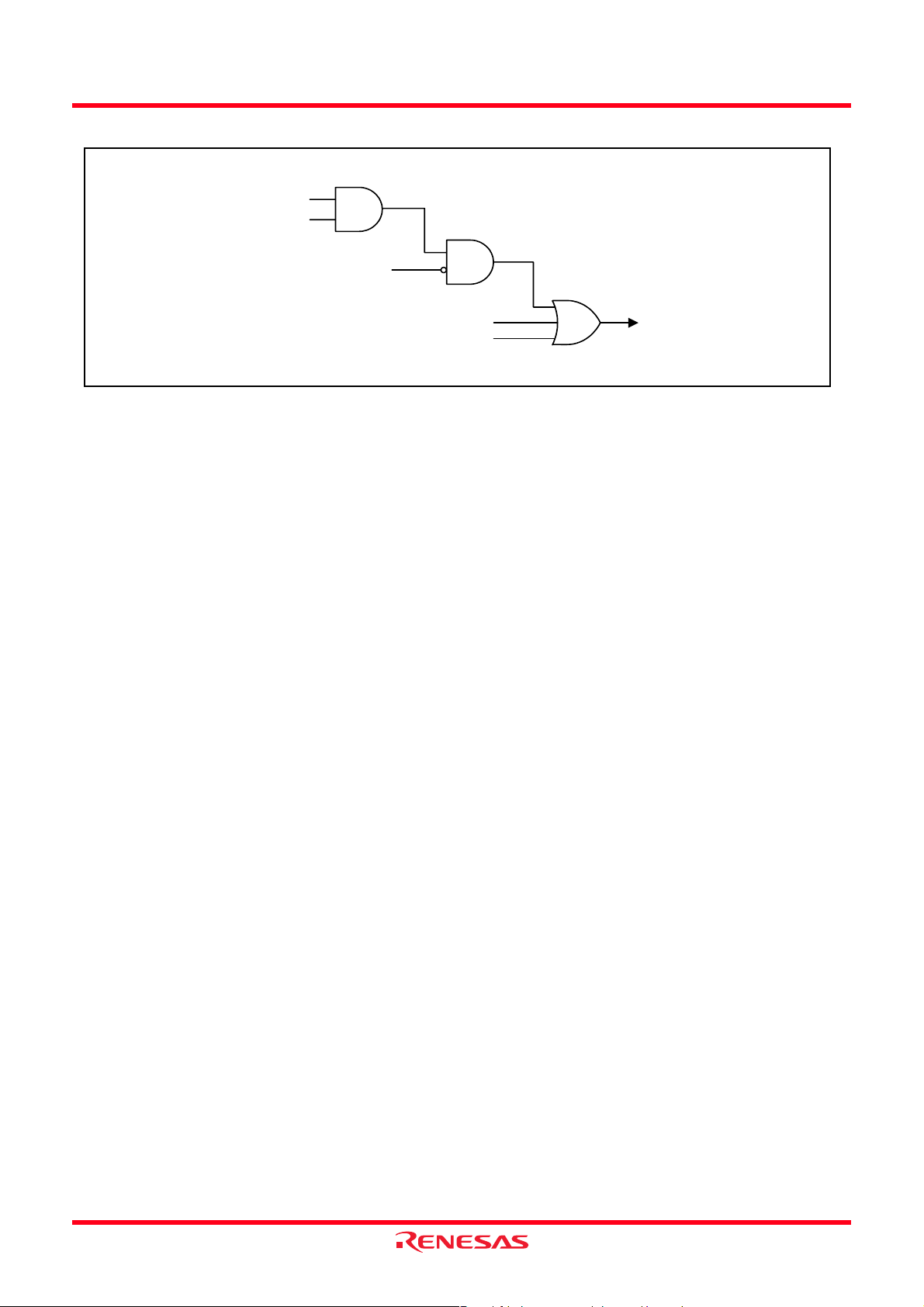
Interrupt request bit
Interrupt enable bit
Interrupt disable flag (I)
BRK instruction
Fig 20. Interrupt control diagram
• Interrupt Disable Flag
The interrupt disable flag is assigned to bit 2 of the processor
status register. This flag controls the acceptance of all interrupt
requests except for the BRK instruction. When this flag is set to
“1”, the acceptance of interrupt requests is disabled. When it is
set to “0”, acceptance of interrupt requests is enabled. This flag is
set to “1” with the SET instruction and set to “0” with the CLI
instruction.
When an interrupt request is accepted, the contents of the
processor status register are pushed onto the stack while the
interrupt disable flag remaines set to “0”. Subsequently, this flag
is automatically set to “1” and multiple interrupts are disabled.
To use multiple interrupts, set this flag to “0” with the CLI
instruction within the interrupt processing routine.
The contents of the processor status register are popped off the
stack with the RTI instruction.
• Interrupt Request Bits
Once an interrupt request is generated, the corresponding
interrupt request bit is set to “1” and remaines “1” until the
request is accepted. When the request is accepted, this bit is
automatically set to “0”.
Each interrupt request bit can be set to “0”, but cannot be set to
“1”, by software.
Reset
Interrupt request
• Interrupt Source Selection
Any of the following combinations can be selected by the
interrupt source selection register (0039
1. INT
0 or timer Z
16).
2. CNTR1 or Serial I/O3 reception
3. Serial I/O2 or timer Z
4 or CNTR2
4. INT
5. A/D conversion or serial I/O3 transmission
• External Interrupt Pin Selection
For external interrupts INT
0 and INT4, the INT0, INT4 interrupt
switch bit in the interrupt edge selection register (bit 6 of address
003A16) can be used to select INT00 and INT40 pin input or
INT
01 and INT41 pin input.
• Interrupt Enable Bits
The interrupt enable bits control the acceptance of t he
corresponding interrupt requests. When an interrupt enable bit is
set to “0”, the acceptance of the corresponding interrupt request
is disabled. If an interrupt request occurs in this condition, the
corresponding interrupt request bit is set to “1”, but the interrupt
request is not accepted. When an interrupt enable bit is set to “1”,
acceptance of the corresponding interrupt request is enabled.
Each interrupt enable bit can be set to “0” or “1” by software.
The interrupt enable bit for an unused interrupt should be set to
“0”.
Rev.1.00 Apr 2, 2007 Page 26 of 117
REJ03B0212-0100
3803 Group (Spec.L)
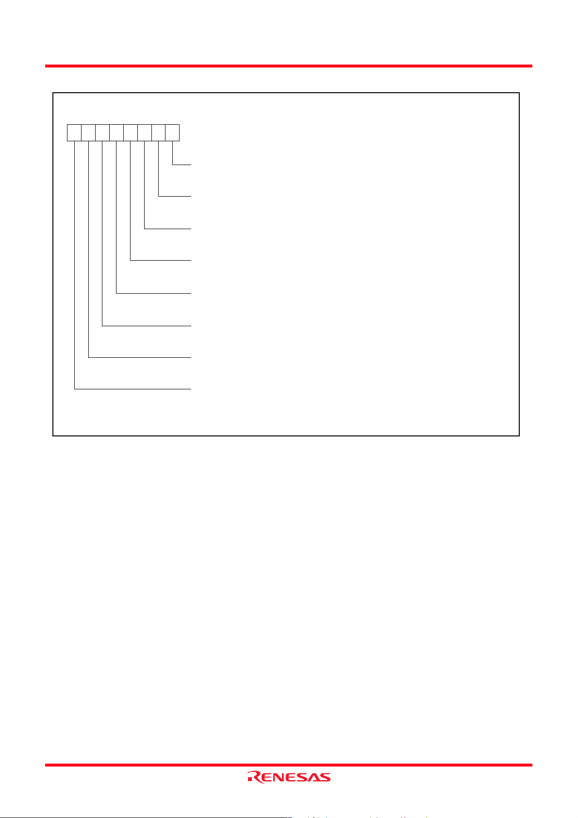
b7 b0
b7 b0
0 : No interrupt request issued
1 : Interrupt request issued
b7 b0
Interrupt edge selection register
(INTEDGE : address 003A
0 interrupt edge selection bit
INT
1 interrupt edge selection bit
INT
16)
Not used (returns “0” when read)
INT
2 interrupt edge selection bit
INT
3 interrupt edge selection bit
INT
4 interrupt edge selection bit
INT
0, INT4 interrupt switch bit
00, INT40 interrupt
0 : INT
01, INT41 interrupt
1 : INT
Not used (returns “0” when read)
Interrupt request register 1
(IREQ1 : address 003C
INT
0/Timer Z interrupt request bit
1 interrupt request bit
INT
Serial I/O1 receive interrupt request bit
Serial I/O1 transmit interrupt request bit
16)
Timer X interrupt request bit
Timer Y interrupt request bit
Timer 1 interrupt request bit
Timer 2 interrupt request bit
Interrupt control register 1
(ICON1 : address 003E
16)
0 : Falling edge active
1 : Rising edge active
0 : Falling edge active
1 : Rising edge active
b7 b0
0 : No interrupt request issued
1 : Interrupt request issued
b7 b0
Interrupt request register 2
(IREQ2 : address 003D
0 interrupt request bit
CNTR
1/Serial I/O3 receive interrupt
CNTR
16)
request bit
Serial I/O2/Timer Z interrupt request bit
INT
2 interrupt request bit
INT
3 interrupt request bit
4/CNTR2 interrupt request bit
INT
AD converter/Serial I/O3 transmit
interrupt request bit
Not used (returns “0” when read)
Interrupt control register 2
(ICON2 : address 003F
16)
0 : Interrupts disabled
1 : Interrupts enabled
b7 b0
INT
0/Timer Z interrupt enable bit
1 interrupt enable bit
INT
Serial I/O1 receive interrupt enable bit
Serial I/O1 transmit interrupt enable bit
Timer X interrupt enable bit
Timer Y interrupt enable bit
Timer 1 interrupt enable bit
Timer 2 interrupt enable bit
Interrupt source selection register
(INTSEL : address 0039
0/Timer Z interrupt source selection bit
INT
0 interrupt
0 : INT
1 : Timer Z interrupt
Serial I/O2/Timer Z interrupt source selection bit
16)
(Do not write “1” to these bits simultaneously.)
0 : Serial I/O2 interrupt
1 : Timer Z interrupt
Not used (Do not write “1”.)
INT
4/CNTR2 interrupt source selection bit
0 : INT
4 interrupt
1 : CNTR
2 interrupt
Not used (Do not write “1”.)
1/Serial I/O3 receive interrupt source selection bit
CNTR
0 : CNTR
1 interrupt
1 : Serial I/O3 receive interrupt
AD converter/Serial I/O3 transmit interrupt source selection bit
0 : A/D converter interrupt
1 : Serial I/O3 transmit interrupt
CNTR0 interrupt enable bit
CNTR
enable bit
Serial I/O2/Timer Z interrupt enable bit
INT
2 interrupt enable bit
INT
3 interrupt enable bit
4/CNTR2 interrupt enable bit
INT
AD converter/Serial I/O3 transmit
interrupt enable bit
Not used (returns “0” when read)
(Do not write “1”.)
0 : Interrupts disabled
1 : Interrupts enabled
1/Serial I/O3 receive interrupt
Fig 21. Structure of interrupt-related registers
Rev.1.00 Apr 2, 2007 Page 27 of 117
REJ03B0212-0100
3803 Group (Spec.L)
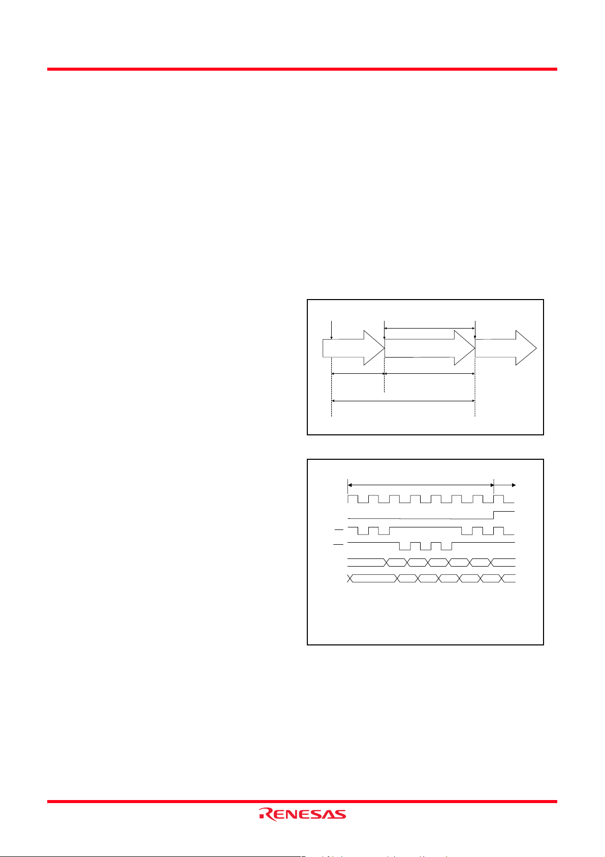
• Interrupt Request Generation, Acceptance, and Handling
Interrupts have the following three phases.
(i) Interrupt Request Generation
An interrupt request is generated by an interrupt source
(external interrupt signal input, timer underflow, etc.) and
the corresponding request bit is set to “1”.
(ii) Interrupt Request Acceptance
Based on the interrupt acceptance timing in each instruction
cycle, the interrupt control circuit determines acceptance
conditions (interrupt request bit, interrupt enable bit, and
interrupt disable flag) and interrupt priority levels for
accepting interrupt requests. When two or more interrupt
requests are generated simultaneo usly, the highest priority
interrupt is accepted. The value of interrupt request bit for
an unaccepted interrupt remains the same and acceptance is
determined at the next interrupt acceptance timing point.
(iii) Handling of Accepted Interrupt Request
The accepted interrupt request is processed.
Figure 22 shows the time up to execution in the interrupt
processing routine, and Figure 23 shows the interrupt sequence.
Figure 24 shows the timing of interrupt request generation,
interrupt request bit, and interrupt request acceptance.
• Interrupt Handling Execution
When interrupt handling is executed, the following operations
are performed automatically.
(1) Once the currently executing instruction is completed, an
interrupt request is accepted.
(2) The contents of the program counters and the processor
status register at this point are pushed onto the stack area in
order from 1 to 3.
1. High-order bits of program counter (PCH)
2. Low-order bits of program counter (PCL)
3. Processor status register (PS)
(3) Concurrently with the push operation, the jump address of
the corresponding interrupt (the start address of the interrupt
processing routine) is transferred from the interrupt vector to
the program counter.
(4) The interrupt request bit for the corresponding interrupt is
set to “0”. Also, the interrupt disable flag is set to “1” and
multiple interrupts are disabled.
(5) The interrupt routine is executed.
(6) When the RTI instruction is executed, the contents of the
registers pushed onto the stack area are popped off in the
order from 3 to 1. Then, the routine that was before running
interrupt processing resumes.
As described above, it is necessary to set the stack pointer and
the jump address in the vector area corresponding to each
interrupt to execute the interrupt processing routine.
<Notes>
The interrupt request bit may be set to “1” in the following cases.
• When setting the external interrupt active edge
Related registers:Interrupt edge selection register
(address 003A
16)
Timer XY mode register (address 002316)
Timer Z mode register (address 002A
16)
• When switching the interrupt sources of an interrupt vector
address where two or more interrupt sources are assigned
Related registers:Interrupt source selection register
(address 0039
16)
If it is not necessary to generate an interrupt synchronized with
these settings, take the following sequence.
(1) Set the corresponding enable bit to “0” (disabled).
(2) Set the interrupt edge selection bit (the active edge switch
bit) or the interrupt source bit.
(3) Set the corresponding interrupt request bit to “0” after one
or more instructions have been executed.
(4) Set the corresponding interrupt enable bit to “1” (enabled).
Interrupt request
generated
Main routine
* When executing DIV instruction
*
0 to 16 cycles
Interrupt request
acceptance
7 to 23 cycles
Interrupt sequence
Stack push and
Vector fetch
7 cycles
Interrupt routine
starts
Interrupt handling
routine
Fig 22. Time up to execution in interrupt routine
Push onto stack
Vector fetch
φ
SYNC
RD
WR
Address bus
Data bus
SYNC : CPU operation code fetch cycle
(This is an internal signal that cannot be observed from the external unit.)
BL, BH: Vector address of each interrupt
AL, AH: Jump destination address of each interrupt
16” or “0116”
SPS : “00
([SPS] is a page selected by the stack page selection bit of CPU mode register.)
S,SPS S-1,SPS S-2,SPS
PC
Not used PCH PCL PS AL AH
BL BH AL,AH
Execute interrupt
routine
Rev.1.00 Apr 2, 2007 Page 28 of 117
REJ03B0212-0100
Fig 23. Interrupt sequence
3803 Group (Spec.L)
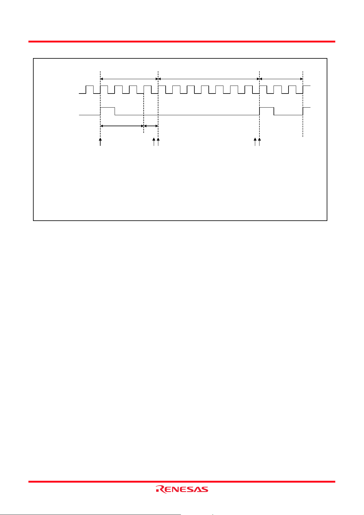
Push onto stack
Vector fetch
Instruction cycle
IR2T3
Internal clock φ
SYNC
Instruction cycle
12
T1
T1 T2 T3 : Interrupt acceptance timing points
IR1 IR2 : Timings points at which the interrupt request bit is set to “1”.
Note : Period 2 indicates the last φ cycle during one instruction cycle.
(1) The interrupt request bit for an interrupt request generated during period 1 is set to “1” at timing point IR1.
(2) The interrupt request bit for an interrupt request generated during period 2 is set to “1” at timing point IR1 or IR2.
The timing point at which the bit is set to “1” varies depending on conditions. When two or more interrupt
requests are generated during the period 2, each request bit may be set to “1” at timing point IR1 or IR2
separately.
IR1T2
Fig 24. Timing of interrupt request generation, interrupt request bit, and interrupt acceptance
Rev.1.00 Apr 2, 2007 Page 29 of 117
REJ03B0212-0100

3803 Group (Spec.L)
TIMERS
•8-bit Timers
The 3803 group (Spec.L) has four 8-bit timers: timer 1, timer 2 ,
timer X, and timer Y.
The timer 1 and timer 2 use one prescaler in common, and the
timer X and timer Y use each prescaler. Those are 8-bit
prescalers. Each of the timers and prescalers has a timer latch or
a prescaler latch.
The division ratio of each timer or prescaler is given by 1/(n + 1),
where n is the value in the corresponding timer or prescaler latch.
All timers are down-counters. When the timer reaches “00
16”, an
underflow occurs at the next count pulse and the contents of the
corresponding timer latch are reloaded into the timer and the
count is continued. When the timer underflows, the interrupt
request bit corresponding to that timer is set to “1”.
• Timer divider
The divider count source is switched by the main clock division
ratio selection bits of CPU mode register (bits 7 and 6 at address
003B
16). When these bits are “00” (high-speed mode) or “01”
(middle-speed mode), X
(low-speed mode), X
IN is selected. When these bits are “10”
CIN is selected.
• Prescaler 12
The prescaler 12 counts the output of the timer divider. The
count source is selected by the timer 12, X count source selection
register among 1/2, 1/4, 1/8, 1/16, 1/32, 1/64, 1/128, 1/256,
1/512, 1/1024 of f(XIN) or f(XCIN).
• Timer 1 and Timer 2
The timer 1 and timer 2 counts the output of prescaler 12 and
periodically set the interrupt request bit.
• Prescaler X and prescaler Y
The prescaler X and prescaler Y count the output of the timer
divider or f(X
X count source selection register (address 000E
Y, Z count source selection register (address 000F
CIN). The count source is selected by the timer 12,
16) and the timer
16) among 1/2,
1/4, 1/8, 1/16, 1/32, 1/64, 1/128, 1/256, 1/512, and 1/1024 of
f(XIN) or f(XCIN); and f(XCIN).
(1) Timer mode
• Mode selection
This mode can be selected by setting “00” to the timer X
operating mode bits (bits 1 and 0) and the timer Y operating
mode bits (bits 5 and 4) of the t imer XY mode re gister (add ress
0023
16).
• Explanation of operation
The timer count operation is started by setting “0” to the timer X
count stop bit (bit 3) and the timer Y count stop bit (bit 7) of the
timer XY mode register (address 0023
When the timer reaches “00
16”, an underflow occurs at the next
16).
count pulse and the contents of timer latch are reloaded into the
timer and the count is continued.
(2) Pulse Output Mode
• Mode selection
This mode can be selected by setting “01” to the timer X
operating mode bits (bits 1 and 0) and the timer Y operating
mode bits (bits 5 and 4) of the t imer XY mode re gister (add ress
16).
0023
• Explanation of operation
The operation is the same as the timer mode’s. Moreover the
pulse which is inverted each time the timer underflows is output
from CNTR
not the output of CNTR
0/CNTR1 pin. Regardless of the timer counting or
0/CNTR1 pin is initialized to the level of
specified by their active edge switch bits when writing to the
timer. When the CNTR0 active edge switch bit (bit 2) and the
CNTR
1 active edge switch bit (bit 6) of the timer XY mode
register (address 0023
16) is “0”, the output starts with “H” level.
When it is “1”, the output starts with “L” level.
Switching the CNTR
reverse the output level of the corresponding CNTR
0 or CNTR1 active edge switch bit will
0 or CNTR1
pin.
• Precautions
Set the double-function port of CNTR
4/P55 to output in this mode.
P5
0/CNTR1 pin and port
• Timer X and Timer Y
The timer X and timer Y can each select one of four operating
modes by setting the timer XY mode register (address 0023
16).
(3) Event Counter Mode
• Mode selection
This mode can be selected by setting “10” to the timer X
operating mode bits (bits 1 and 0) and the timer Y operating
mode bits (bits 5 and 4) of the t imer XY mode re gister (add ress
0023
16).
• Explanation of operation
The operation is the same as the timer mode’s except that the
timer counts signals input from the CNTR
valid edge for the count operation depends on the CNTR
edge switch bit (bit 2) or the CNTR
of the timer XY mode register (address 0023
0 or CNTR1 pin. The
0 active
1 active edge switch bit (bit 6)
16). When it is “0”,
the rising edge is valid. When it is “1”, the falling edge is valid.
• Precautions
Set the double-function port of CNTR
P5
4/P55 to input in this mode.
0/CNTR1 pin and port
Rev.1.00 Apr 2, 2007 Page 30 of 117
REJ03B0212-0100

3803 Group (Spec.L)
(4) Pulse Width Measurement Mode
• Mode selection
This mode can be selected by setting “11” to the timer X
operating mode bits (bits 1 and 0) and the timer Y operating
mode bits (bits 5 and 4) of the timer XY mode register (address
002316).
• Explanation of operation
When the CNTR
active edge switch bit (bit 6) of the timer XY mode register
(address 0023
falling edge of CNTR
edge of input (“L” term). When it is “0”, the timer counts during
the term of one rising edge input until the next falling edge input
(“H” term).
• Precautions
Set the double-function port of CNTR
P5
4/P55 to input in this mode.
The count operation can be stopped by setting “1” to the timer X
count stop bit (bit 3) and the timer Y count stop bit (bit 7) of the
timer XY mode register (address 0023
bit is set to “1” each time the timer underflows.
• Precautions when switching count source
When switching the count source by the timer 12, X and Y count
source selection bits, the value of timer count is altered in
inconsiderable amount owing to generating of thin pulses on the
count input signals.
Therefore, select the timer count source before setting the value
to the prescaler and the timer.
0 active edge switch bit (bit 2) or the CNTR1
16) is “1”, the timer counts during the term of one
0/CNTR1 pin input until the next rising
0/CNTR1 pin and port
16). The interrupt request
Rev.1.00 Apr 2, 2007 Page 31 of 117
REJ03B0212-0100

3803 Group (Spec.L)
XIN
CIN
X
“00”
“11”
“10”
Main clock
division ratio
selection bits
P5
(1/2, 1/4, 1/8, 1/16, 1/32, 1/64, 1/128, 1/256, 1/512, 1/1024)
Divider
Clock fo r timer 12
4/CNTR0
Port P54
direction register
Clock for timer X
Clock fo r timer Y
f(XCIN)
CNTR
edge switch bit
Pulse output mode
Count source selection bit
Count source
selection bit
0 active
“0”
“1”
4
Port P5
latch
Pulse width
measurement
mode
Event
counter
mode
CNTR
edge switch bit
Timer mode
Pulse output mode
Timer X count stop bit
0 active
“1”
“0”
Data bus
Prescaler X latch (8)
Prescaler X (8)
Q
Toggle flip-flop
Q
R
Data bus
Timer X latch (8)
Timer X (8)
T
Timer X latch write pulse
Pulse output mode
To timer X interrupt
request bit
0 interrupt
To CNTR
request bit
P55/CNTR1
direction register
Clock for timer Y
f(XCIN)
5
Port P5
Pulse output mode
Clock for timer 12
1 active
CNTR
edge switch bit
“0”
“1”
Port P5
latch
Pulse width
measurement
mode
5
Timer mode
Pulse output mode
Event
Timer Y count stop bit
counter
mode
CNTR
1 active
edge switch bit
Prescaler 12 latch (8)
Prescaler 12 (8)
Prescaler Y latch (8)
Prescaler Y (8)
“1”
Q
Toggle flip-flop
Q
“0”
Data bus
Fig 25. Block diagram of timer X, timer Y, timer 1, and timer 2
R
Timer 1 latch (8)
Timer 1 (8)
Timer Y latch (8)
Timer Y (8)
T
Timer Y latch write pulse
Pulse output mode
Timer 2 latch (8)
Timer 2 (8)
To timer Y interrupt
request bit
1 interrupt
To CNTR
request bit
To timer 2 interrupt
request bit
To timer 1 interrupt
request bit
Rev.1.00 Apr 2, 2007 Page 32 of 117
REJ03B0212-0100

3803 Group (Spec.L)
b7
b0
Timer XY mode register
(TM : address 0023
16)
Timer X operating mode bits
b1 b0
0 0: Timer mode
0 1: Pulse output mode
1 0: Event counter mode
1 1: Pulse width measurement mode
0 active edge switch bit
CNTR
0: Interrupt at falling edge
Count at rising edge in event counter mode
1: Interrupt at rising edge
Count at falling edge in event counter mode
Timer X count stop bit
0: Count start
1: Count stop
Timer Y operating mode bits
b5 b4
0 0: Timer mode
0 1: Pulse output mode
1 0: Event counter mode
1 1: Pulse width measurement mode
Fig 26. Structure of timer XY mode register
1 active edge switch bit
CNTR
0: Interrupt at falling edge
Count at rising edge in event counter mode
1: Interrupt at rising edge
Count at falling edge in event counter mode
Timer Y count stop bit
0: Count start
1: Count stop
Rev.1.00 Apr 2, 2007 Page 33 of 117
REJ03B0212-0100

3803 Group (Spec.L)
b7 b0
Timer 12, X count source selection register
(T12XCSS : address 000E
16)
Timer 12 count source selection bits
b3 b2 b1 b0
0000:f(X
IN)/2 or f(XCIN)/2
0001:f(XIN)/4 or f(XCIN)/4
0 0 1 0 : f(X
0 0 1 1 : f(X
IN)/8 or f(XCIN)/8
IN)/16 or f(XCIN)/16
0 1 0 0 : f(XIN)/32 or f(XCIN)/32
0 1 0 1 : f(XIN)/64 or f(XCIN)/64
0 1 1 0 : f(XIN)/128 or f(XCIN)/128
0 1 1 1 : f(X
IN)/256 or f(XCIN)/256
1 0 0 0 : f(XIN)/512 or f(XCIN)/512
1 0 0 1 : f(X
IN)/1024 or f(XCIN)/1024
Timer X count source selection bits
b7 b6 b5 b4
0000:f(X
IN)/2 or f(XCIN)/2
0001:f(XIN)/4 or f(XCIN)/4
0 0 1 0 : f(XIN)/8 or f(XCIN)/8
0 0 1 1 : f(X
IN)/16 or f(XCIN)/16
0 1 0 0 : f(XIN)/32 or f(XCIN)/32
0 1 0 1 : f(XIN)/64 or f(XCIN)/64
0 1 1 0 : f(X
IN)/128 or f(XCIN)/128
0 1 1 1 : f(XIN)/256 or f(XCIN)/256
1 0 0 0 : f(X
1 0 0 1 : f(X
1 0 1 0 : f(X
IN)/512 or f(XCIN)/512
IN)/1024 or f(XCIN)/1024
CIN)
1 0 1 0 :
1 0 1 1 :
1 1 0 0 :
1 1 0 1 :
1 1 1 0 :
1 1 1 1 :
1 0 1 1 :
1 1 0 0 :
1 1 0 1 :
1 1 1 0 :
1 1 1 1 :
Not used
Not used
b7 b0
Timer Y, Z count source selection register
(TYZCSS : address 000F
16)
Timer Y count source selection bits
b3 b2 b1 b0
0000:f(X
0001:f(X
0 0 1 0 : f(X
0 0 1 1 : f(X
IN)/2 or f(XCIN)/2
IN)/4 or f(XCIN)/4
IN)/8 or f(XCIN)/8
IN)/16 or f(XCIN)/16
0 1 0 0 : f(XIN)/32 or f(XCIN)/32
0 1 0 1 : f(X
IN)/64 or f(XCIN)/64
0 1 1 0 : f(XIN)/128 or f(XCIN)/128
0 1 1 1 : f(X
1 0 0 0 : f(X
IN)/256 or f(XCIN)/256
IN)/512 or f(XCIN)/512
1 0 0 1 : f(XIN)/1024 or f(XCIN)/1024
1 0 1 0 : f(XCIN)
Timer Z count source selection bits
b7 b6 b5 b4
0000:f(XIN)/2 or f(XCIN)/2
0001:f(XIN)/4 or f(XCIN)/4
0 0 1 0 : f(X
IN)/8 or f(XCIN)/8
0 0 1 1 : f(XIN)/16 or f(XCIN)/16
0 1 0 0 : f(X
0 1 0 1 : f(X
IN)/32 or f(XCIN)/32
IN)/64 or f(XCIN)/64
0 1 1 0 : f(XIN)/128 or f(XCIN)/128
0 1 1 1 : f(X
IN)/256 or f(XCIN)/256
1 0 0 0 : f(XIN)/512 or f(XCIN)/512
1 0 0 1 : f(XIN)/1024 or f(XCIN)/1024
1 0 1 0 : f(X
CIN)
1 0 1 1 :
1 1 0 0 :
1 1 0 1 :
1 1 1 0 :
1 1 1 1 :
1 0 1 1 :
1 1 0 0 :
1 1 0 1 :
1 1 1 0 :
1 1 1 1 :
Not used
Not used
Fig 27. Structure of timer 12, X and timer Y, Z count source selection registers
Rev.1.00 Apr 2, 2007 Page 34 of 117
REJ03B0212-0100

3803 Group (Spec.L)
• 16-bit Timer
The timer Z is a 16-bit timer. When the timer reaches “000016”,
an underflow occurs at the next count pulse and the
corresponding timer latch is reloaded into the timer and the count
is continued. When the timer underflows, the interrupt request bit
corresponding to the timer Z is set to “1”.
When reading/writing to the timer Z, perform reading/writing to
both the high-order byte and the low-order byte. When reading
the timer Z, read from the high-order byte first, followed by the
low-order byte. Do not perform the writing to the timer Z
between read operation of the high-order byte and read operation
of the low-order byte. When writing to the timer Z, write to the
low-order byte first, followed by the high-order byte. Do not
perform the reading to the timer Z between write operation of the
low-order byte and write operation of the high-order byte.
The timer Z can select the count source by the timer Z count
source selection bits of timer Y, Z count source selection register
(bits 7 to 4 at address 000F
16).
Timer Z can select one of seven operating modes by setting the
timer Z mode register (address 002A16).
(1) Timer mode
• Mode selection
This mode can be selected by setting “000” to the timer Z
operating mode bits (bits 2 to 0) and setting “0” to the
timer/event counter mode switch bit (b7) of the timer Z mode
register (address 002A
16).
• Count source selection
In high- or middle-speed mode, 1/2, 1/4, 1/8, 1/16, 1/32, 1/64,
1/128, 1/256, 1/512 or 1/1024 of f (XIN); or f(XCIN) can be
selected as the count source.
In low-speed mode, 1/2, 1/4, 1/8, 1/16, 1/32, 1/64, 1/128, 1/256,
1/512 or 1/1024 of f(X
CIN); or f(XCIN) can be selected as the
count source.
• Interrupt
When an underflow occurs, the INT
(bit 0) of the interrupt request register 1 (address 003C
0/timer Z interrupt request bit
16) is set to
“1”.
• Explanation of operation
During timer stop, usually write data to a latch and a timer at the
same time to set the timer value.
The timer count operation is started by setting “0” to the timer Z
count stop bit (bit 6) of the timer Z mode register (address
002A16).
When the timer reaches “0000
16”, an underflow occurs at the
next count pulse and the contents of timer latch are reloaded into
the timer and the count is continued.
When writing data to the timer during operation, the data is
written only into the latch. Then the new latch value is reloaded
into the timer at the next underflow.
(2) Event counter mode
• Mode selection
This mode can be selected by setting “000” to the timer Z
operating mode bits (bits 2 to 0) and setting “1” to the
timer/event counter mode switch bit (bit 7) of the timer Z mode
register (address 002A16).
The valid edge for the count operation depends on the CNTR
active edge switch bit (bit 5) of the timer Z mode register
(address 002A
16). When it is “0”, the rising edge is valid. When
it is “1”, the falling edge is valid.
• Interrupt
The interrupt at an underflow is the same as the timer mode’s.
• Explanation of operation
The operation is the same as the timer mode’s.
Set the double-function port of CNTR
2 pin and port P47 to input
in this mode.
Figure 30 shows the timing chart of the timer/event counter
mode.
(3) P ulse output mode
• Mode selection
This mode can be selected by setting “001” to the timer Z
operating mode bits (bits 2 to 0) and setting “0” to the
timer/event counter mode switch bit (b7) of the timer Z mode
register (address 002A16).
• Count source selection
In high- or middle-speed mode, 1/2, 1/4, 1/8, 1/16, 1/32, 1/64,
1/128, 1/256, 1/512 or 1/1024 of f (X
IN); or f(XCIN) can be
selected as the count source.
In low-speed mode, 1/2, 1/4, 1/8, 1/16, 1/32, 1/64, 1/128, 1/256,
1/512 or 1/1024 of f(X
CIN); or f(XCIN) can be selected as the
count source.
• Interrupt
The interrupt at an underflow is the same as the timer mode’s.
• Explanation of operation
The operation is the same as the timer mode’s. Moreover the
pulse which is inverted each time the timer underflows is output
from CNTR2 pin. When the CNTR2 active edge switch bit (bit 5)
of the timer Z mode register (address 002A
16) is “0”, the output
starts with “H” level. When it is “1”, the output starts with “L”
level.
• Precautions
The double-function port of CNTR
2 pin an d port P47 is
automatically set to the timer pulse output port in this mode.
The output from CNTR
on CNTR
2 active edge switch bit by writing to the timer.
When the value of the CNTR
the output level of CNTR
2 pin is initialized to the level depending
2 active edge switch bit is changed,
2 pin is inverted.
Figure 31 shows the timing chart of the pulse output mode.
2
Rev.1.00 Apr 2, 2007 Page 35 of 117
REJ03B0212-0100

3803 Group (Spec.L)
(4) Pulse period measurement mode
• Mode selection
This mode can be selected by setting “010” to the timer Z
operating mode bits (bits 2 to 0) and setting “0” to the
timer/event counter mode switch bit (b7) of the timer Z mode
register (address 002A16).
• Count source selection
In high- or middle-speed mode, 1/2, 1/4, 1/8, 1/16, 1/32, 1/64,
1/128, 1/256, 1/512 or 1/1024 of f (X
IN); or f(XCIN) can be
selected as the count source.
In low-speed mode, 1/2, 1/4, 1/8, 1/16, 1/32, 1/64, 1/128, 1/256,
1/512 or 1/1024 of f(X
CIN); or f(XCIN) can be selected as the
count source.
• Interrupt
The interrupt at an underflow is the same as the timer mode’s.
When the pulse period measurement is completed, the
INT4/CNTR2 interrupt request bit (bit 5) of the interrupt request
register 2 (address 003D
16) is set to “1”.
• Explanation of operation
The cycle of the pulse which is input from the CNTR2 pin is
measured. When the CNTR
timer Z mode register (address 002A
during the term from one falling edge of CNTR
2 active edge switch bit (bit 5) of the
16) is “0”, the timer counts
2 pin input to the
next falling edge. When it is “1”, the timer counts during the
term from one rising edge input to the next rising edge input.
When the valid edge of measurement completion/start is
detected, the 1’s complement of the timer value is written to the
timer latch and “FFFF
16” is set to the timer.
Furthermore when the timer underflows, the timer Z interrupt
request occurs and “FFFF16” is set to the timer. When reading
the timer Z, the value of the timer latch (measured value) is read.
The measured value is retained until the next measurement
completion.
• Precautions
Set the double-function port of CNTR2 pin and port P47 to input
in this mode.
A read-out of timer value is impossible in this mode. The timer
can be written to only during timer stop (no measurement of
pulse period).
Since the timer latch in this mode is specialized for the read-out
of measured values, do not perform any write operation during
measurement.
“FFFF
16” is set to the timer when the timer underflows or when
the valid edge of measurement start/completion is detected.
Consequently, the timer value at start of pulse period
measurement depends on the timer value just before
measurement start.
Figure 32 shows the timing chart of the pulse period
measurement mode.
(5) Pulse width measurement mode
• Mode selection
This mode can be selected by setting “011” to the timer Z
operating mode bits (bits 2 to 0) and setting “0” to the
timer/event counter mode switch bit (b7) of the timer Z mode
register (address 002A
16).
• Count source selection
In high- or middle-speed mode, 1/2, 1/4, 1/8, 1/16, 1/32, 1/64,
1/128, 1/256, 1/512 or 1/1024 of f (X
IN); or f(XCIN) can be
selected as the count source.
In low-speed mode, 1/2, 1/4, 1/8, 1/16, 1/32, 1/64, 1/128, 1/256,
1/512 or 1/1024 of f(X
CIN); or f(XCIN) can be selected as the
count source.
• Interrupt
The interrupt at an underflow is the same as the timer mode’s.
When the pulse widths measurement is completed, the
INT4/CNTR2 interrupt request bit (bit 5) of the interrupt request
register 2 (address 003D
16) is set to “1”.
• Explanation of operation
The pulse width which is input from the CNTR2 pin is measured.
When the CNTR
mode register (address 002A
2 active edge switch bit (bit 5) of the timer Z
16) is “0”, the timer counts during
the term from one rising edge input to the next falling edge input
(“H” term). When it is “1”, the timer counts during the term from
one falling edge of CNTR
2 pin input to the next rising edge of
input (“L” term).
When the valid edge of measurement completion is detected, the
1’s complement of the timer value is written to the timer latch.
When the valid edge of measurement completion/start is
detected, “FFFF
16” is set to the timer.
When the timer Z underflows, the timer Z interrupt occurs and
“FFFF16” is set to the timer Z. When reading the timer Z, the
value of the timer latch (measured value) is read. The measured
value is retained until the next measurement completion.
• Precautions
Set the double-function port of CNTR
2 pin and port P47 to input
in this mode.
A read-out of timer value is impossible in this mode. The timer
can be written to only during timer stop (no measurement of
pulse widths).
Since the timer latch in this mode is specialized for the read-out
of measured values, do not perform any write operation during
measurement.
“FFFF
16” is set to the timer when the timer underflows or when
the valid edge of measurement start/completion is detected.
Consequently, the timer value at start of pulse width
measurement depends on the timer value just before
measurement start.
Figure 33 shows the timing chart of the pulse width measurement
mode.
Rev.1.00 Apr 2, 2007 Page 36 of 117
REJ03B0212-0100

3803 Group (Spec.L)
(6) Programmable waveform generating mode
• Mode selection
This mode can be selected by setting “100” to the timer Z
operating mode bits (bits 2 to 0) and setting “0” to the
timer/event counter mode switch bit (b7) of the timer Z mode
register (address 002A16).
• Count source selection
In high- or middle-speed mode, 1/2, 1/4, 1/8, 1/16, 1/32, 1/64,
1/128, 1/256, 1/512 or 1/1024 of f (X
IN); or f(XCIN) can be
selected as the count source.
In low-speed mode, 1/2, 1/4, 1/8, 1/16, 1/32, 1/64, 1/128, 1/256,
1/512 or 1/1024 of f(X
CIN); or f(XCIN) can be selected as the
count source.
• Interrupt
The interrupt at an underflow is the same as the timer mode’s.
• Explanation of operation
The operation is the same as the timer mode’s. Moreover the
timer outputs the data set in the output level latch (bit 4) of the
timer Z mode register (address 002A
16) from the CNTR2 pin
each time the timer underflows.
Changing the value of the output level latch and the timer latch
after an underflow makes it possible to output an optional
waveform from the CNTR2 pin.
• Precautions
The double-function port of CNTR
2 pin an d port P47 is
automatically set to the programmable waveform generating port
in this mode.
Figure 34 shows the timing chart of the programmable waveform
generating mode.
(7) Programmable one-shot generating mode
• Mode selection
This mode can be selected by setting “101” to the timer Z
operating mode bits (bits 2 to 0) and setting “0” to the
timer/event counter mode switch bit (b7) of the timer Z mode
register (address 002A
16).
• Count source selection
In high- or middle-speed mode, 1/2, 1/4, 1/8, 1/16, 1/32, 1/64,
1/128, 1/256, 1/512 or 1/1024 of f (X
IN); or f(XCIN) can be
selected as the count source.
• Interrupt
The interrupt at an underflow is the same as the timer mode’s.
The trigger to generate one-shot pulse can be selected by the INT
active edge selection bit (bit 1) of the interrupt edge selection
register (address 003A
16). When it is “0”, the falling edge active is
selected; when it is “1”, the rising edge active is selected.
When the valid edge of the INT1 pin is detected, the INT1
interrupt request bit (bit 1) of the interrupt request register 1
(address 003C
16) is set to “1”.
• Explanation of operation
1. “H” one-shot pulse; Bit 5 of timer Z mode register = “0”
The output level of the CNTR
2 pin is initialized to “L” at
mode selection. When trigger generation (input signal to
1 pin) is detected, “H” is output from the CNTR2 pin.
INT
When an underflow occurs, “L” is output. The “H” one-shot
pulse width is set by the setting value to the timer Z register
low-order and high-order. When trigger generating is
detected during timer count stop, although “H” is output
from the CNTR
2 pin, “H” output state continues because an
underflow does not occur.
2. “L” one-shot pulse; Bit 5 of timer Z mode register = “ 1”
The output level of the CNTR
2 pin is initialized to “H” at
mode selection. When trigger generation (input signal to
1 pin) is detected, “L” is output from the CNTR2 pin.
INT
When an underflow occurs, “H” is output. The “L” one-shot
pulse width is set by the setting value to the timer Z loworder and high-order. When trigger generating is detected
during timer count stop, although “L” is output from the
2 pin, “L” output state continues because an under-
CNTR
flow does not occur.
• Precautions
Set the double-function port of INT
1 pin and port P42 to input in
this mode.
The double-function port of CNTR
2 pin an d port P47 is
automatically set to the programmable one-shot generating port
in this mode.
This mode cannot be used in low-speed mode.
If the value of the CNTR2 active edge switch bit is changed
during one-shot generating enabled or generating one-shot pulse,
then the output level from CNTR
2 pin changes.
Figure 35 shows the timing chart of the programmable one-shot
generating mode.
<Notes regarding all modes>
• Timer Z write control
Which write control can be selected by the timer Z write control
bit (bit 3) of the timer Z mode register (address 002A16), writing
data to both the latch and the timer at the same time or writing
data only to the latch.
When the operation “writing data only to the latch” is selected,
the value is set to the timer latch by writing data to the address of
timer Z and the timer is updated at next underflow. After reset
release, the operation “writing data to both the latch and the timer
at the same time” is selected, and the value is set to both the latch
and the timer at the same time by writing data to the address of
timer Z.
In the case of writing data only to the latch, if writing data to the
latch and an underflow are performed almost at the same time,
the timer value may become undefined.
• Timer Z read control
A read-out of timer value is impossible in pulse period
measurement mode and pulse width measurement mode. In the
other modes, a read-out of timer value is possible regardless of
count operating or stopped.
However, a read-out of timer latch value is impossible.
• Switch of interrupt active edge of CNTR
1
Each interrupt active edge depends on setting of the CNTR2
2 and INT1
active edge switch bit and the INT1 active edge selection bit.
• Switch of count source
When switching the count source by the timer Z count source
selection bits, the value of timer count is altered in
inconsiderable amount owing to generating of thin pulses on the
count input signals.
Therefore, select the timer count source before setting the value
to the prescaler and the timer.
• Usage of CNTR
2 pin as normal I/O port P47
To use the CNTR2 pin as normal I/O port P47, set timer Z
operating mode bits (b2, b1, b0) of timer Z mode register
(address 002A
16) to “000”.
Rev.1.00 Apr 2, 2007 Page 37 of 117
REJ03B0212-0100

3803 Group (Spec.L)
“001”
“100”
“101”
Timer Z operating
mode bits
7
Port P4
direction register
P42/INT1
Programmable one-shot
generating mode
Output level latch
Port P4
latch
Pulse period measurement mode
Pulse width measurement mode
CNTR
2 active edge
switch bit
Programmable one-shot
generating circuit
Programmable waveform
generating mode
D
Q
T
Pulse output mode
T
7
Timer Z low-order latch
Timer Z low-order
2 active edge switch bit
CNTR
S
“0”
Q
Q
Pulse output mode
“1”
Timer Z high-order latch
Timer Z high-order
Programmable one-shot
“1”
generating mode
“0”
Data bus
To INT
1 interrupt
request bit
To timer Z interrupt
request bit
P47/SRDY2/
CNTR
2
CNTR2 active edge
switch bit
XIN
XCIN
Fig 28. Block diagram of timer Z
Edge detection circuit
“1”
Clock for tim e r z
Divider
f(XCIN)
Count source
selection bit
Timer/Event
counter mode
switch bit
“0”
(1/2, 1/4, 1/8, 1/16, 1/32, 1/64, 1/128, 1/256, 1/512, 1/1024)
To CNTR2 interrupt
“1”
“0”
Timer Z count stop bit
request bit
Rev.1.00 Apr 2, 2007 Page 38 of 117
REJ03B0212-0100

3803 Group (Spec.L)
b7 b0
Timer Z mode register
(TZM : address 002A
16)
Timer Z operating mode bits
b2 b1 b0
0 0 0 : Timer/Event counter mode
0 0 1 : Pulse output mode
0 1 0 : Pulse period measurement mode
0 1 1 : Pulse width measurement mode
1 0 0 : Programmable waveform generating mode
1 0 1 : Programmable one-shot generating mode
1 1 0 : Not available
1 1 1 : Not available
Timer Z write control bit
0 : Writing data to both latch and timer simultaneously
1 : Writing data only to latch
Output level latch
0 : “L” output
1 : “H” output
CNTR
2 active edge switch bit
0 : •Event counter mode: Count at rising edge
•Pulse output mode: Start outputting “H”
•Pulse period measurement mode: Measurement between two falling edges
•Pulse width measurement mode: Measurement of “H” term
•Programmable one-shot generating mode: After start outputting “L”,
“H” one-shot pulse generated
•Interrupt at falling edge
1 : •Event counter mode: Count at falling edge
•Pulse output mode: Start outputting “L”
•Pulse period measurement mode: Measurement between two rising edges
•Pulse width measurement mode: Measurement of “L” term
•Programmable one-shot generating mode: After start outputting “H”,
“L” one-shot pulse generated
•Interrupt at rising edge
Timer Z count stop bit
0 : Count start
1 : Count stop
Timer/Event counter mode switch bit
(1)
0 : Timer mode
1 : Event counter mode
Note 1: When selecting the modes except the timer/event counter mode, set “0” to this bit.
Fig 29. Structure of timer Z mode register
Rev.1.00 Apr 2, 2007 Page 39 of 117
REJ03B0212-0100

3803 Group (Spec.L)
FFFF16
TL
000016
TR TR TR
TL : Value set to timer latch
TR : Timer interrupt request
Fig 30. Timing chart of timer/event counter mode
FFFF16
TL
000016
TR TR TR TR
Waveform output
CNTR2 pin
from
CNTR
TL : Value set to timer latch
TR : Timer interrupt request
2 : CNTR2 interrupt request
CNTR
(CNTR
2 active edge switch bit = “0”; Falling edge active)
2 CNTR2
Fig 31. Timing chart of pulse output mode
Rev.1.00 Apr 2, 2007 Page 40 of 117
REJ03B0212-0100

3803 Group (Spec.L)
000016
FFFF16
T3
T2
T1
TR TR
T2 T3
FFFF16FFFF16 + T1
Signal input from
2 pin
CNTR
CNTR
2
CNTR2 CNTR2 CNTR2
CNTR2 of rising edge active
TR : Timer interrupt request
2 : CNTR2 interrupt request
CNTR
Fig 32. Timing chart of pulse period measurement mode (Measuring term b etween two rising edges)
000016
T3
T2
T1
FFFF16
TR
Signal input from
2 pin
CNTR
FFFF16 + T2
CNTR
2
CNTR2 interrupt of rising edge active; Measurement of “L” width
TR : Timer interrupt request
CNTR
2 : CNTR2 interrupt request
Fig 33. Timing chart of pulse width measurement mode (Measuring “L” term)
Rev.1.00 Apr 2, 2007 Page 41 of 117
REJ03B0212-0100
T1T3
CNTR2 CNTR2

3803 Group (Spec.L)
FFFF
000016
16
T3
L
T2
T1
Signal output from
CNTR
2 pin
L
T1
TR TR
2 CNTR2
CNTR
L : Timer initial value
TR : Timer interrupt request
2 : CNTR2 interrupt request
CNTR
(CNTR
Fig 34. Timing chart of programmable waveform generating mode
16
FFFF
2 active edge switch bit = “0”; Falling edge active)
L
Signal input from
1 pin
INT
TR TR
T3
T2
TR TR
TR
Signal output from
2 pin
CNTR
L
CNTR
L
2 CNTR2
L
L : One-shot pulse width
TR : Timer interrupt request
2 : CNTR2 interrupt request
CNTR
(CNTR
Fig 35. Timing chart of programmable one-shot generating mode (“H” one-shot pulse generating)
2 active edge switch bit = “0”; Falling edge active)
Rev.1.00 Apr 2, 2007 Page 42 of 117
REJ03B0212-0100

3803 Group (Spec.L)
SERIAL INTERFACE
• Serial I/O1
Serial I/O1 can be used as either clock synchronous or
asynchronous (UART) serial I/O. A dedicated timer is also
provided for baud rate generation.
Data bus
Address 001816
Receive buffer register 1
P44/RXD1
6/SCLK1
P4
f(X
IN)
(f(XCIN) in low-speed mode)
P47/SRDY1/CNTR2
P45/TXD1
BRG count source selection bit
1/4
F/F
Receive shift register 1
Shift clock
Serial I/O1 synchronous clock selection bit
Frequency division ratio 1/(n+1)
Transmit shift register 1
(1) Clock Synchronous Serial I/O Mode
Clock synchronous serial I/O1 mode can be selected by setting
the serial I/O1 mode selection bit of the serial I/O1 control
register (bit 6 of address 001A
16) to “1”.
For clock synchronous serial I/O, the transmitter and the receiver
must use the same clock. If an internal clock is used, transfer is
started by a write signal to the transmit/receive buffer register.
Baud rate generator 1
Address 001C
Clock control circuitFalling-edge detector
Shift clock
Serial I/O1 control register
Receive buffe r fu ll flag (R BF)
Receive interrupt request (RI)
Clock control circuit
1/4
16
Transmit interrupt source selection bit
Address 001A16
Transmit sh ift completion flag (TS C)
Transmit inter ru p t re q u e s t (T I)
Transmit buffer register 1
Address 0018
Data bus
16
Serial I/O1 status register
Transmit buffer empty flag (TBE)
Address 0019
Fig 36. Block diagram of clock synchronous serial I/O1
Transfer shift clock
(1/2 to 1/2048 of the internal
clock, or an external clock)
Serial output T
XD1
Serial input RXD1
Receive enable signal S
Write pulse to receive/transmit
buffer register 1 (address 0018
RDY1
16)
TBE = 0
Notes 1: As the transmit interrupt (TI), which can be selected, either when the transmit buffer has emptied (TBE=1) or after the transmit
shift operation has ended (TSC=1), by setting the transmit interrupt source selection bit (TIC) of the serial I/O1 control register.
2: If data is written to the transmit buffer register when TSC=0, the transmit clock is generated continuously and serial data is output
continuously from the T
XD pin.
3: The receive interrupt (RI) is set when the receive buffer full flag (RBF) becomes “1”.
D0 D1 D2 D3 D4 D5 D6
D0 D1 D2 D3 D4 D5 D6
TBE = 1
TSC = 0
16
D7
D7
RBF = 1
TSC = 1
Overrun error (OE)
detection
Fig 37. Operation of clock synchronous serial I/O1
Rev.1.00 Apr 2, 2007 Page 43 of 117
REJ03B0212-0100

3803 Group (Spec.L)
(2) Asynchronous Serial I/O (UART) Mode
Clock asynchronous serial I/O mode (UART) can be selected by
clearing the serial I/O1 mode selection bit (b6) of the serial I/O1
control register to “0”.
Eight serial data transfer formats can be selected, and the transfer
formats used by a transmitter and receiver must be identical.
Data bus
Address 0018
SP detector
Frequency division ratio 1/(n+1)
Baud rate generator
ST/SP/PA generator
Transmit shift register 1
Transmit buffer register 1
Data bus
P44/RXD1
6/SCLK1
P4
(f(XCIN) in low-speed mode)
f(XIN)
P45/TXD1
ST detector
OE
Character length selection bit
7 bits
8 bits
BRG count source selection bit
1/4
Character length selection bit
Receive buffer register 1
Receive shift register 1
PE FE
Serial I/O1 synchronous clock selection bit
The transmit and receive shift registers each have a buffer, but
the two buffers have the same address in a memory. Since the
shift register cannot be written to or read from directly, transmit
data is written to the transmit buffer register, and receive data is
read from the receive buffer register.
The transmit buffer register can also hold the next data to be
transmitted, and the receive buffer register can hold a character
while the next character is being received.
Address 001C
Address 0018
Serial I/O1 control register
16
Receive buffer full flag (RBF)
Receive interrupt request (RI)
Clock control circuit
16
1/16
Transmit interrupt source selection bit
Serial I/O1 status register
16
Address 001A
1/16
16
UART1 control register
Address 001B
Transmit shift
completion flag (TSC)
Transmit interrupt request (TI)
Transmit buffer empty flag (TBE)
Address 0019
16
16
Fig 38. Block diagram of UART serial I/O1
Transmit or
receive clock
Transmit buffer
write signal
Serial output
T
Receive buffer
read signal
Serial input
R
Notes 1: Error flag detection occurs at the same time that the RBF flag becomes “1” (at 1st stop bit, during reception).
TBE=0
TSC=0
TBE=1
XD1
XD1
2: As the transmit interrupt (TI), when either the TBE or TSC flag becomes “1”, can be selected to occur depending on the setting of the transmit interrupt source
selection bit (TIC) of the serial I/O1 control register.
3: The receive interrupt (RI) is set when the RBF flag becomes “1”.
4: After data is written to the transmit buffer when TSC=1, 0.5 to 1.5 cycles of the data shift cycle are necessary until changing to TSC=0.
TBE=0
1 start bit
7 or 8 data bit
1 or 0 parity bit
1 or 2 stop bit (s)
TBE=1
RBF=1
Fig 39. Operation of UART serial I/O1
STD0 D1 SP D0 D1ST SP
Generated at 2nd bit in 2-stop-bit mode
RBF=0
STD0 D1 SP D0 D1ST SP
TSC=1*
RBF=1
Rev.1.00 Apr 2, 2007 Page 44 of 117
REJ03B0212-0100

3803 Group (Spec.L)
[Transmit Buffer Register 1/Receive Buffer Register 1
(TB1/RB1)] 001816
The transmit buffer register 1 and the receive buffer register 1 are
located at the same address. The transmit buffer is write-only and
the receive buffer is read-only. If a character bit length is 7 bits,
the MSB of data stored in the receive buffer is “0”.
[Serial I/O1 Status Register (SIO1STS)] 001916
The read-only serial I/O1 status register consists of seven flags
(bits 0 to 6) which indicate the operating status of the serial I/O1
function and various errors.
Three of the flags (bits 4 to 6) are valid only in UART mode.
The receive buffer full flag (bit 1) is cleared to “0” when the
receive buffer register is read.
If there is an error, it is detected at the same time that data is
transferred from the receive shift register to the receive buffer
register, and the receive buffer full flag is set. A write to the
serial I/O1 status register clears all the error flags OE, PE, FE,
and SE (bit 3 to bit 6, respectively). Writing “0” to the seria l I/O1
enable bit SIOE (bit 7 of the serial I/O1 control register) also
clears all the status flags, including the error flags.
Bits 0 to 6 of the serial I/O1 status register are initialize d to “0” at
reset, but if the transmit enable bit (bit 4) of the serial I/O1
control register has been set to “1”, the transmit shift completion
flag (bit 2) and the transmit buffer empty flag (bit 0) become “1”.
[Serial I/O1 Control Register (SIO1CON)] 001A
16
The serial I/O1 control register consists of eight control bits for
the serial I/O1 function.
[UART1 Control Register (UART1CON)] 001B
16
The UART control register consists of four control bits (bits 0 to
3) which are valid when asynchronous serial I/O is selected and
set the data format of an data transfer, and one bit (bit 4) which is
always valid and sets the output structure of the P4
5/TXD1 pin.
[Baud Rate Generator 1 (BRG1)] 001C16
The baud rate generator determines the baud rate for serial
transfer.
The baud rate generator divides the frequency of the count source
by 1/(n + 1), where n is the value written to the baud rate
generator.
Rev.1.00 Apr 2, 2007 Page 45 of 117
REJ03B0212-0100

3803 Group (Spec.L)
b7
b7 b0
b0
Serial I/O1 status register
(SIO1STS : address 0019
16)
Transmit buffer empty flag (TBE)
0: Buffer full
1: Buffer empty
Receive buffer full flag (RBF)
0: Buffer empty
1: Buffer full
Transmit shift completion flag (TSC)
0: Transmit shift in progress
1: Transmit shift completed
Overrun error flag (OE)
0: No error
1: Overrun error
Parity error flag (PE)
0: No error
1: Parity error
Framing error flag (FE)
0: No error
1: Framing error
Summing error flag (SE)
0: (OE) U (PE) U (FE)=0
1: (OE) U (PE) U (FE)=1
Not used (returns “1” when read)
UART1 control register
(UART1CON : address 001B
16)
Character length selection bit (CHAS)
0: 8 bits
1: 7 bits
Parity enable bit (PARE)
0: Parity checking disabled
1: Parity checking enabled
Parity selection bit (PARS)
0: Even parity
1: Odd parity
Stop bit length selection bit (STPS)
0: 1 stop bit
1: 2 stop bits
P4
5/TXD1 P-channel output disable bit (POFF)
0: CMOS output (in output mode)
1: N-channel open drain output (in output mode)
Not used (return “1” when read)
b7 b0
Serial I/O1 control register
(SIO1CON : address 001A
16)
BRG count source selection bit (CSS)
0: f(X
IN) (f(XCIN) in low-speed mode)
1: f(X
IN)/4 (f(XCIN)/4 in low-speed mode)
Serial I/O1 synchronous clock selection bit (SCS)
0: BRG output divided by 4 when clock synchronous
serial I/O1 is selected, BRG output divided by 16
when UART is selected.
1: External clock input when clock synchronous serial
I/O1 is selected, external clock input divided by 16
when UART is selected.
S
RDY1 output enable bit (SRDY)
0: P4
7 pin operates as normal I/O pin
7 pin operates as SRDY1 output pin
1: P4
Transmit interrupt source selection bit (TIC)
0: Interrupt when transmit buffer has emptied
1: Interrupt when transmit shift operation is completed
Transmit enable bit (TE)
0: Transmit disabled
1: Transmit enabled
Receive enable bit (RE)
0: Receive disabled
1: Receive enabled
Serial I/O1 mode selection bit (SIOM)
0: Clock asynchronous (UART) serial I/O
1: Clock synchronous serial I/O
Serial I/O1 enable bit (SIOE)
0: Serial I/O1 disabled
(pins P4
4 to P47 operate as normal I/O pins)
1: Serial I/O1 enabled
(pins P4
4 to P47 operate as serial I/O1 pins)
Fig 40. Structure of serial I/O1 control registers
Rev.1.00 Apr 2, 2007 Page 46 of 117
REJ03B0212-0100

3803 Group (Spec.L)
<Notes concerning serial I/O1>
1. Notes when selecting clock synchronous serial I/O
1.1 Stop of transmission operation
•Note
Clear the serial I/O1 enable bit and the transmit enable bit to
“0” (serial I/O and transmit disabled).
•Reason
Since transmission is not stopped and the transmission circuit
is not initialized even if only the serial I/O1 enable bit is
cleared to “0” (serial I/O disabled), the internal tr ansmission is
running (in this case, since pins T
XD1, RXD1, SCLK1, and
SRDY1 function as I/O ports, the transmission data is not
output). When data is written to the transmit buffer register in
this state, data starts to be shifted to the transmit shift register.
When the serial I/O1 enable bit is set to “1” at this time, the
data during internally shifting is output to the T
XD1 pin and an
operation failure occurs.
1.2 Stop of receive operation
•Note
Clear the receive enable bit to “0” (receive disabled), or clear
the serial I/O1 enable bit to “0” (serial I/O disabled).
1.3 Stop of transmit/receive operation
• Note
Clear both the transmit enable bit and receive enable bit to “0”
(transmit and receive disabled).
(when data is transmitted and received in the clock
synchronous serial I/O mode, any one of data transmission and
reception cannot be stopped.)
•Reason
In the clock synchronous serial I/O mode, the same clock is
used for transmission and reception. If any one of transmission
and reception is disabled, a bit error occurs because
transmission and reception cannot be synchronized.
In this mode, the clock circuit of the transmission circuit also
operates for data reception. Accordingly, the transmission
circuit does not stop by clearing only the transmit enable bit to
“0” (transmit disabled). Also, the transmission circuit is not
initialized by clearing the serial I/O1 enable bit to “0” (serial
I/O disabled) (refer to 1.1).
2. Notes when selecting clock asynchronous serial I/O
2.1 Stop of transmission operation
•Note
Clear the transmit enable bit to “0” (transmit disabled). The
transmission operation does not stop by clearing the serial
I/O1 enable bit to “0”.
•Reason
Since transmission is not stopped and the transmission circuit
is not initialized even if only the serial I/O1 enable bit is
cleared to “0” (serial I/O disabled), the internal tr a ns mi ssi on is
running (in this case, since pins T
XD1, RXD1, SCLK1, and
SRDY1 function as I/O ports, the transmission data is not
output). When data is written to the transmit buffer register in
this state, data starts to be shifted to the transmit shift register.
When the serial I/O1 enable bit is set to “1” at this time, the
data during internally shifting is output to the T
XD1 pin and an
operation failure occurs.
2.2 Stop of receive operation
•Note
Clear the receive enable bit to “0” (receive disabled).
2.3 Stop of transmit/receive operation
• Note 1 (only transmission operation is stopped)
Clear the transmit enable bit to “0” (transmit disabled). The
transmission operation does not stop by clearing the serial
I/O1 enable bit to “0”.
•Reason
Since transmission is not stopped and the transmission circuit
is not initialized even if only the serial I/O1 enable bit is
cleared to “0” (serial I/O disabled), the internal tr a ns mi ssi on is
running (in this case, since pins T
XD1, RXD1, SCLK1, and
SRDY1 function as I/O ports, the transmission data is not
output). When data is written to the transmit buffer register in
this state, data starts to be shifted to the transmit shift register.
When the serial I/O1 enable bit is set to “1” at this time, the
data during internally shifting is output to the T
XD1 pin and an
operation failure occurs.
• Note 2 (only receive operation is stopped)
Clear the receive enable bit to “0” (receive disabled).
Rev.1.00 Apr 2, 2007 Page 47 of 117
REJ03B0212-0100

3803 Group (Spec.L)
3. SRDY1 output of reception side
•Note
When signals are output from the S
RDY1 pin on the reception
side by using an external clock in the clock synchronous serial
I/O mode, set all of the receive enable bit, the S
RDY1 output
enable bit, and the transmit enable bit to “1” (transmit
enabled).
4. Setting serial I/O1 control register again
•Note
Set the serial I/O1 control register again after the transmission
and the reception circuits are reset by clearing both the
transmit enable bit and the receive enable bit to “0”.
Clear both the transmit enable
bit (TE) and the receive enable
bit (RE) to “0”
Set the bits 0 to 3 and bit 6 of
the serial I/O1 control register
Set both the transmit enable bit
(TE) and the receive enable bit
(RE), or one of them to “1”
Can be set with the
LDM instruction at
the same time
7. Transmit interrupt request when transmit enable bit is set
•Note
When using the transmit interrupt, take the following
sequence.
1. Set the serial I/O1 transmit interrupt enable bit to “0” (disabled).
2. Set the transmit enable bit to “1”.
3. Set the serial I/O1 transmit interrupt request bit to “0” after
1 or more instruction has executed.
4. Set the serial I/O1 transmit interrupt enable bit to “1”
(enabled).
•Reason
When the transmit enable bit is set to “1”, the transmit buffer
empty flag and the transmit shift register shift completion flag
are also set to “1”. Therefore, regardless of selecting which
timing for the generating of transmit interrupts, the interrupt
request is generated and the transmit interrupt request bit is set
at this point.
5.Data transmission control with referring to transmit shift
register completion flag
• Note
After the transmit data is written to the transmit buffe r register,
the transmit shift register completion flag changes from “1” to
“0” with a delay of 0.5 to 1.5 shift clocks. When data
transmission is controlled with referring to the flag after
writing the data to the transmit buffer register, note the delay.
6. Transmission control when external clock is selected
•Note
When an external clock is used as the synchronous clock for
data transmission, set the transmit enable bit to “1” at “H” of
CLK1 input level. Also, write data to the transmit buffer
the S
register at “H” of the S
CLK1 input level.
Rev.1.00 Apr 2, 2007 Page 48 of 117
REJ03B0212-0100

3803 Group (Spec.L)
• Serial I/O2
The serial I/O2 function can be used only for clock synchronous
serial I/O.
For clock synchronous serial I/O2, the transmitter and the
receiver must use the same clock. If the internal clock is used,
transfer is started by a write signal to the serial I/O2 register
(address 001F
[Serial I/O2 Control Register (SIO2CON)] 001D16
The serial I/O2 control register contains eight bits which control
various serial I/O2 functions.
16).
b7
b0
Serial I/O2 control register
(SIO2CON : address 001D
Internal synchronous clock selection bits
b2 b1 b0
000:f(XIN)/8 (f(XCIN)/8 in low-speed mode)
001:f(X
010:f(X
011:f(X
110:f(X
111:f(X
Serial I/O2 port selection bit
0: I/O port
1: S
S
RDY2 output enable bit
0: I/O port
1: SRDY2 signal output
Transfer direction selection bit
0: LSB first
1: MSB first
Serial I/O2 synchronous clock selection bit
0: External clock
1: Internal clock
P5
1/SOUT2 P-channel output disable bit
0: CMOS output (in output mode)
1: N-channel open drain output (in output mode)
IN)/16 (f(XCIN)/16 in low-speed mode)
IN)/32 (f(XCIN)/32 in low-speed mode)
IN)/64 (f(XCIN)/64 in low-speed mode)
IN)/128 f(XCIN)/128 in low-speed mode)
IN)/256 (f(XCIN)/256 in low-speed mode)
OUT2, SCLK2 signal output
16)
Fig 41. Structure of Serial I/O2 control register
f(XIN)
(f(XCIN) in low-speed mode)
P53/SRDY2
RDY2 output enable bit
S
P52/SCLK2
Serial I/O2 port selection bit
P51/SOUT2
Serial I/O2 port selection bit
P50/SIN2
3 latch
P5
“0”
“1”
P52 latch
“0”
“1”
P5
1 latch
“0”
“1”
SRDY2
Synchronization
Serial I/O2 synchronous
clock selection bit
circuit
External clock
SCLK2
1/8
1/16
1/32
1/64
Divider
1/128
1/256
“1”
“0”
Serial I/O counter 2 (3)
Serial I/O2 register (8)
Internal synchronous
clock selection bits
Address 001F16
Data bus
Serial I/O2
interrupt request
Fig 42. Block diagram of serial I/O2
Rev.1.00 Apr 2, 2007 Page 49 of 117
REJ03B0212-0100

3803 Group (Spec.L)
Transfer clock
Serial I/O2 register
Serial I/O2 output SOUT2
Serial I/O2 input SIN2
Receive enable signal SRDY2
Notes1:When the internal clock is selected as the transfer clock, the divide ratio of f(X
2:When the internal clock is selected as the transfer clock, the S
(1)
write signal
setting bits 0 to 2 of the serial I/O2 control register.
OUT2 pin goes to high impedance after transfer completion.
Fig 43. Timing of serial I/O2
(2)
D7D0 D1 D2 D3 D4 D5 D6
Serial I/O2 interrupt request bit set
IN), or (f(XCIN) in low-speed mode, can be selected by
Rev.1.00 Apr 2, 2007 Page 50 of 117
REJ03B0212-0100

3803 Group (Spec.L)
t
• Serial I/O3
Serial I/O3 can be used as either clock synchronous or
asynchronous (UART) serial I/O3. A dedicated timer is also
provided for baud rate generation.
Data bus
Address 003016
Receive buffer register 3
P34/RXD3
6/SCLK3
P3
f(X
IN)
(f(XCIN) in low-speed mode)
P37/SRDY3
P35/TXD3
BRG count source selection bit
F/F
1/4
Receive shift register 3
Shift clock
Serial I/O3 synchronous clock selection bit
Frequency division ratio 1/(n+1)
Baud rate generator 3
Shift clock
Transmit shift register 3
(1) Clock Synchronous Serial I/O Mode
Clock synchronous serial I/O3 mode can be selected by setting
the serial I/O3 mode selection bit of the serial I/O3 control
register (bit 6 of address 0032
16) to “1”.
For clock synchronous serial I/O, the transmitter and the receiver
must use the same clock. If an internal clock is used, transfer is
started by a write signal to the transmit/receive buffer register.
Clock control circuit
Address 002F
Clock control circuitFalling-edge detector
Serial I/O3 control register
Receive buffer full flag (RBF)
Receive interrupt request (RI)
1/4
16
Transmit shift completion flag (TSC)
Transmit interrupt source selection bit
Address 003216
Transmit interrupt request (TI)
Transmit buffer register 3
Address 0030
Data bus
16
Serial I/O3 status register
Transmit buffer empty flag (TBE)
Address 0031
Fig 44. Block diagram of clock synchronous serial I/O3
Transfer shift clock
(1/2 to 1/2048 of the internal
clock, or an external clock)
Serial output T
XD3
Serial input RXD3
Receive enable signal S
Write pulse to receive/transmit
buffer register (address 0030
RDY3
16)
TBE = 0
Notes 1: As the transmit interrupt (TI), which can be selected, either when the transmit buffer has emptied (TBE=1) or after the transmit
shift operation has ended (TSC=1), by setting the transmit interrupt source selection bit (TIC) of the serial I/O3 control register.
2: If data is written to the transmit buffer register when TSC=0, the transmit clock is generated continuously and serial data is outpu
continuously from the TXD pin.
3: The receive interrupt (RI) is set when the receive buffer full flag (RBF) becomes “1”.
D0 D1 D2 D3 D4 D5 D6
D0 D1 D2 D3 D4 D5 D6
TBE = 1
TSC = 0
Overrun error (OE)
detection
16
D7
D7
RBF = 1
TSC = 1
Fig 45. Operation of clock synchronous serial I/O3
Rev.1.00 Apr 2, 2007 Page 51 of 117
REJ03B0212-0100

3803 Group (Spec.L)
(2) Asynchronous Serial I/O (UART) Mode
Clock asynchronous serial I/O mode (UART) can be selected by
clearing the serial I/O3 mode selection bit (b6) of the serial I/O3
control register to “0”.
Eight serial data transfer formats can be selected, and the transfer
formats used by a transmitter and receiver must be identical.
Data bus
Address 0030
SP detector
Frequency division ratio 1/(n+1)
Baud rate generator 3
ST/SP/PA generator
Transmit shift register 3
Transmit buffer register 3
Data bus
P34/RXD3
6/SCLK3
P3
(f(XCIN) in low-speed mode)
f(XIN)
P35/TXD3
ST detector
OE
Character length selection bit
7 bits
8 bits
BRG count source selection bit
1/4
Character length selection bit
Receive buffer register 3
Receive shift register 3
PE FE
Serial I/O3 synchronous clock selection bit
The transmit and receive shift registers each have a buffer, but
the two buffers have the same address in a memory. Since the
shift register cannot be written to or read from directly, transmit
data is written to the transmit buffer register, and receive data is
read from the receive buffer register.
The transmit buffer register can also hold the next data to be
transmitted, and the receive buffer register can hold a character
while the next character is being received.
Address 002F
Address 0030
Serial I/O3 control register
16
Receive buffer full flag (RBF)
Receive interrupt request (RI)
Clock control circuit
16
1/16
Transmit interrupt source selection bit
Serial I/O3 status register
16
Address 0032
16
1/16
UART3 control register
Address 0033
Transmit shift
completion flag (TSC)
Transmit interrupt request (TI)
Transmit buffer empty flag (TBE)
Address 0031
16
16
Fig 46. Block diagram of UART serial I/O3
Transmit or
receive clock
Transmit buffer
write signal
Serial output
T
XD3
Receive buffer
read signal
Serial input
R
XD3
Notes1: Error flag detection occurs at the same time that the RBF flag becomes “1” (at 1st stop bit, during reception).
TBE=0
TSC=0
TBE=1
2: As the transmit interrupt (TI), when either the TBE or TSC flag becomes “1”, can be selected to occur depending on the setting of the transmit interrupt source
selection bit (TIC) of the serial I/O3 control register.
3: The receive interrupt (RI) is set when the RBF flag becomes “1”.
4: After data is written to the transmit buffer when TSC=1, 0.5 to 1.5 cycles of the data shift cycle are necessary until changing to TSC=0.
TBE=0
1 start bit
7 or 8 data bit
1 or 0 parity bit
1 or 2 stop bit (s)
RBF=1
Fig 47. Operation of UART serial I/O3
TBE=1
STD0 D1 SP D0 D1ST SP
* Generated at 2nd bit in 2-stop-bit mode
RBF=0
STD0 D1 SP D0 D1ST SP
TSC=1*
RBF=1
Rev.1.00 Apr 2, 2007 Page 52 of 117
REJ03B0212-0100

3803 Group (Spec.L)
[Transmit Buffer Register 3/Receive Buffer Register 3
(TB3/RB3)] 003016
The transmit buffer register 3 and the receive buffer register 3 are
located at the same address. The transmit buffer is write-only and
the receive buffer is read-only. If a character bit length is 7 bits,
the MSB of data stored in the receive buffer is “0”.
[Serial I/O3 Status Register (SIO3STS)] 003116
The read-only serial I/O3 status register consists of seven flags
(bits 0 to 6) which indicate the operating status of the serial I/O3
function and various errors.
Three of the flags (bits 4 to 6) are valid only in UART mode.
The receive buffer full flag (bit 1) is cleared to “0” when the
receive buffer register is read.
If there is an error, it is detected at the same time that data is
transferred from the receive shift register to the receive buffer
register, and the receive buffer full flag is set. A write to the
serial I/O3 status register clears all the error flags OE, PE, FE,
and SE (bit 3 to bit 6, respectively). Writing “0” to the seria l I/O3
enable bit SIOE (bit 7 of the serial I/O3 control register) also
clears all the status flags, including the error flags.
Bits 0 to 6 of the serial I/O3 status register are initialize d to “0” at
reset, but if the transmit enable bit (bit 4) of the serial I/O3
control register has been set to “1”, the transmit shift completion
flag (bit 2) and the transmit buffer empty flag (bit 0) become “1”.
[Serial I/O3 Control Register (SIO3CON)] 0032
16
The serial I/O3 control register consists of eight control bits for
the serial I/O3 function.
[UART3 Control Register (UART3CON)] 0033
16
The UART control register consists of four control bits (bits 0 to
3) which are valid when asynchronous serial I/O is selected and
set the data format of an data transfer, and one bit (bit 4) which is
always valid and sets the output structure of the P3
5/TXD3 pin.
[Baud Rate Generator 3 (BRG3)] 002F16
The baud rate generator determines the baud rate for serial
transfer.
The baud rate generator divides the frequency of the count source
by 1/(n + 1), where n is the value written to the baud rate
generator.
Rev.1.00 Apr 2, 2007 Page 53 of 117
REJ03B0212-0100

3803 Group (Spec.L)
b7
b7 b0
b0
Serial I/O3 status register
(SIO3STS : address 0031
16)
Transmit buffer empty flag (TBE)
0: Buffer full
1: Buffer empty
Receive buffer full flag (RBF)
0: Buffer empty
1: Buffer full
Transmit shift completion flag (TSC)
0: Transmit shift in progress
1: Transmit shift completed
Overrun error flag (OE)
0: No error
1: Overrun error
Parity error flag (PE)
0: No error
1: Parity error
Framing error flag (FE)
0: No error
1: Framing error
Summing error flag (SE)
0: (OE) U (PE) U (FE)=0
1: (OE) U (PE) U (FE)=1
Not used (returns “1” when read)
UART3 control register
(UART3CON : address 0033
16)
Character length selection bit (CHAS)
0: 8 bits
1: 7 bits
Parity enable bit (PARE)
0: Parity checking disabled
1: Parity checking enabled
Parity selection bit (PARS)
0: Even parity
1: Odd parity
Stop bit length selection bit (STPS)
0: 1 stop bit
1: 2 stop bits
P3
5/TXD3 P-channel output disable bit (POFF)
0: CMOS output (in output mode)
1: N-channel open drain output (in output mode)
Not used (return “1” when read)
b7 b0
Serial I/O3 control register
(SIO3CON : address 0032
16)
BRG count source selection bit (CSS)
0: f(X
IN) (f(XCIN) in low-speed mode)
1: f(X
IN)/4 (f(XCIN)/4 in low-speed mode)
Serial I/O3 synchronous clock selection bit (SCS)
0: BRG output divided by 4 when clock synchronous
serial I/O3 is selected, BRG output divided by 16
when UART is selected.
1: External clock input when clock synchronous serial
I/O3 is selected, external clock input divided by 16
when UART is selected.
S
RDY3 output enable bit (SRDY)
0: P3
7 pin operates as normal I/O pin
7 pin operates as SRDY3 output pin
1: P3
Transmit interrupt source selection bit (TIC)
0: Interrupt when transmit buffer has emptied
1: Interrupt when transmit shift operation is completed
Transmit enable bit (TE)
0: Transmit disabled
1: Transmit enabled
Receive enable bit (RE)
0: Receive disabled
1: Receive enabled
Serial I/O3 mode selection bit (SIOM)
0: Clock asynchronous (UART) serial I/O
1: Clock synchronous serial I/O
Serial I/O3 enable bit (SIOE)
0: Serial I/O3 disabled
(pins P3
4 to P37 operate as normal I/O pins)
1: Serial I/O3 enabled
(pins P3
4 to P37 operate as serial I/O3 pins)
Fig 48. Structure of serial I/O3 control registers
Rev.1.00 Apr 2, 2007 Page 54 of 117
REJ03B0212-0100

3803 Group (Spec.L)
<Notes concerning serial I/O3>
1. Notes when selecting clock synchronous serial I/O
1.1 Stop of transmission operation
•Note
Clear the serial I/O3 enable bit and the transmit enable bit to
“0” (serial I/O and transmit disabled).
•Reason
Since transmission is not stopped and the transmission circuit
is not initialized even if only the serial I/O3 enable bit is
cleared to “0” (serial I/O disabled), the internal tr ansmission is
running (in this case, since pins T
XD3, RXD3, SCLK3, and
SRDY3 function as I/O ports, the transmission data is not
output). When data is written to the transmit buffer register in
this state, data starts to be shifted to the transmit shift register.
When the serial I/O3 enable bit is set to “1” at this time, the
data during internally shifting is output to the T
XD3 pin and an
operation failure occurs.
1.2 Stop of receive operation
•Note
Clear the receive enable bit to “0” (receive disabled), or clear
the serial I/O3 enable bit to “0” (serial I/O disabled).
1.3 Stop of transmit/receive operation
• Note
Clear both the transmit enable bit and receive enable bit to “0”
(transmit and receive disabled).
(when data is transmitted and received in the clock
synchronous serial I/O mode, any one of data transmission and
reception cannot be stopped.)
•Reason
In the clock synchronous serial I/O mode, the same clock is
used for transmission and reception. If any one of transmission
and reception is disabled, a bit error occurs because
transmission and reception cannot be synchronized.
In this mode, the clock circuit of the transmission circuit also
operates for data reception. Accordingly, the transmission
circuit does not stop by clearing only the transmit enable bit to
“0” (transmit disabled). Also, the transmission circuit is not
initialized by clearing the serial I/O3 enable bit to “0” (serial
I/O disabled) (refer to 1.1).
2. Notes when selecting clock asynchronous serial I/O
2.1 Stop of transmission operation
•Note
Clear the transmit enable bit to “0” (transmit disabled). The
transmission operation does not stop by clearing the serial
I/O3 enable bit to “0”.
•Reason
Since transmission is not stopped and the transmission circuit
is not initialized even if only the serial I/O3 enable bit is
cleared to “0” (serial I/O disabled), the internal tr a ns mi ssi on is
running (in this case, since pins T
XD3, RXD3, SCLK3, and
SRDY3 function as I/O ports, the transmission data is not
output). When data is written to the transmit buffer register in
this state, data starts to be shifted to the transmit shift register.
When the serial I/O3 enable bit is set to “1” at this time, the
data during internally shifting is output to the T
XD3 pin and an
operation failure occurs.
2.2 Stop of receive operation
•Note
Clear the receive enable bit to “0” (receive disabled).
2.3 Stop of transmit/receive operation
• Note 1 (only transmission operation is stopped)
Clear the transmit enable bit to “0” (transmit disabled). The
transmission operation does not stop by clearing the serial
I/O3 enable bit to “0”.
•Reason
Since transmission is not stopped and the transmission circuit
is not initialized even if only the serial I/O3 enable bit is
cleared to “0” (serial I/O disabled), the internal tr a ns mi ssi on is
running (in this case, since pins T
XD3, RXD3, SCLK3, and
SRDY3 function as I/O ports, the transmission data is not
output). When data is written to the transmit buffer register in
this state, data starts to be shifted to the transmit shift register.
When the serial I/O3 enable bit is set to “1” at this time, the
data during internally shifting is output to the T
XD3 pin and an
operation failure occurs.
• Note 2 (only receive operation is stopped)
Clear the receive enable bit to “0” (receive disabled).
Rev.1.00 Apr 2, 2007 Page 55 of 117
REJ03B0212-0100

3803 Group (Spec.L)
3. SRDY3 output of reception side
•Note
When signals are output from the S
RDY3 pin on the reception
side by using an external clock in the clock synchronous serial
I/O mode, set all of the receive enable bit, the SRDY3 output
enable bit, and the transmit enable bit to “1” (transmit
enabled).
4. Setting serial I/O3 control register again
•Note
Set the serial I/O3 control register again after the transmission
and the reception circuits are reset by clearing both the
transmit enable bit and the receive enable bit to “0”.
Clear both the transmit enable
bit (TE) and the receive enable
bit (RE) to “0”
Set the bits 0 to 3 and bit 6 of
the serial I/O3 control register
Set both the transmit enable bit
(TE) and the receive enable bit
(RE), or one of them to “1”
Can be set with the
LDM instruction at
the same time
7. Transmit interrupt request when transmit enable bit is set
•Note
When using the transmit interrupt, take the following
sequence.
1. Set the serial I/O3 transmit interrupt enable bit to “0” (disabled).
2. Set the transmit enable bit to “1”.
3. Set the serial I/O3 transmit interrupt request bit to “0” after
1 or more instruction has executed.
4. Set the serial I/O3 transmit interrupt enable bit to “1”
(enabled).
•Reason
When the transmit enable bit is set to “1”, the transmit buffer
empty flag and the transmit shift register shift completion flag
are also set to “1”. Therefore, regardless of selecting which
timing for the generating of transmit interrupts, the interrupt
request is generated and the transmit interrupt request bit is set
at this point.
5.Data transmission control with referring to transmit shift
register completion flag
•Note
After the transmit data is written to the transmit buffe r register,
the transmit shift register completion flag changes from “1” to
“0” with a delay of 0.5 to 1.5 shift clocks. When data
transmission is controlled with referring to the flag after
writing the data to the transmit buffer register, note the delay.
6. Transmission control when external clock is selected
•Note
When an external clock is used as the synchronous clock for
data transmission, set the transmit enable bit to “1” at “H” of
CLK3 input level. Also, write data to the transmit buffer
the S
register at “H” of the SCLK input level.
Rev.1.00 Apr 2, 2007 Page 56 of 117
REJ03B0212-0100

3803 Group (Spec.L)
PULSE WIDTH MODULATION (PWM)
The 3803 group (Spec.H QzROM version) has PWM functions
with an 8-bit resolution, based on a signal that is the clock input
IN or that clock input divided by 2 or the clock input XCIN or
X
that clock input divided by 2 in low-speed mode.
• Data Setting
The PWM output pin also functions as port P5
6. Set the PWM
period by the PWM prescaler, and set the “H” term of output
pulse by the PWM register.
If the value in the PWM prescaler is n and the value in the PWM
register is m (where n = 0 to 255 and m = 0 to 255):
PWM period = 255 × (n+1) / f(X
IN)
= 31.875 × (n+1) µs
(when f(XIN) = 8 MHz, count source selection bit = “0”)
Output pulse “H” term = PWM period × m / 255
= 0.125 × (n+1) × m µs
(when f(X
IN) = 8 MHz, count source selection bit = “0”)
Data bus
• PWM Operation
When bit 0 (PWM enable bit) of the PWM control register is set
to “1”, operation starts by initializing the PWM output circuit,
and pulses are output starting at an “H”.
If the PWM register or PWM prescaler is updated during PWM
output, the pulses will change in the cycle after the one in which
the change was made.
31.875 × m × (n+1)
255
PWM output
T = [31.875
m : Contents of PWM register
n : Contents of PWM prescaler
T : PWM period
(when f(X
IN) = 8 MHz, count source selection bit = “0”)
µs
× (n+1)] µs
Fig 49. Timing of PWM period
prescaler pre-latch
prescaler latch
Count source
selection bit
(XCIN at low-
X
speed mode)
1/2
“0”
“1”
IN
PWM prescaler
Fig 50. Block diagram of PWM function
PWM
Transfer control circuit
PWM
PWM
register pre-latch
PWM
register latch
PWM register
Port P5
6 latch
PWM function enable bit
Port P5
6
Rev.1.00 Apr 2, 2007 Page 57 of 117
REJ03B0212-0100

3803 Group (Spec.L)
b7 b0
Fig 51. Structure of PWM control register
A
PWM output
PWM control register
(PWMCON: address 002B
PWM function enable bit
0: PWM disabled
1: PWM enabled
Count source selection bit
IN) (f(XCIN) at low-speed mode)
0: f(X
IN)/2 (f(XCIN)/2 at low-speed mode)
1: f(X
Not used
(return “0” when read)
B C
T T T2
16)
B
=
TCT2
PWM register
(Changes “H” term from “A” to “ B”.)
write signal
PWM prescaler
(Changes PWM period from “T” to “T2”.)
write signal
When the contents of the PWM register or PWM prescaler have changed,
the PWM output will change from the next period after the change.
Fig 52. PWM output timing when PWM register or PWM prescaler is changed
<Notes>
The PWM starts after the PWM function enable bit is set to enable and “L” level is output from the PWM pin.
The length of this “L” level output is as follows:
n1+
-----------------------
2×fXIN()
n1
--------------- - sec
fXIN()
sec
+
(Count source selection bit = 0, where n is the value set in the prescaler)
(Count source selection bit = 1, where n is the value set in the prescaler)
Rev.1.00 Apr 2, 2007 Page 58 of 117
REJ03B0212-0100

3803 Group (Spec.L)
A/D CONVERTER (successive approximation type)
[AD Conversion Register 1, 2 (AD1, AD2)] 0035
16,
003816
The AD conversion register is a read-only register that stores the
result of an A/D conversion. When reading this register during an
A/D conversion, the previous conversion result is read.
Bit 7 of the AD conversion register 2 is the conversion mode
selection bit. When this bit is set to “0”, the A/D converter
becomes the 10-bit A/D mode. When this bit is set to “1”, that
becomes the 8-bit A/D mode. The conversion result of the 8-bit
A/D mode is stored in the AD conversion register 1. As for 10-bit
A/D mode, not only 10-bit reading but also only high-order 8-bit
reading of conversion result can be performed by selecting the
reading procedure of the AD conversion registers 1, 2 after A/D
conversion is completed (in Figure 54).
As for 10-bit A/D mode, the 8-bit reading inclined to MSB is
performed when reading the AD converter register 1 after A/D
conversion is started; and when the AD converter register 1 is
read after reading the AD converter register 2, the 8-bit reading
inclined to LSB is performed.
[AD/DA Control Register (ADCON)] 0034
16
The AD/DA control register controls the A/D conversion
process. Bits 0 to 2 and bit 4 select a specific analog input pin.
Bit 3 signals the completion of an A/D conversion. The value of
this bit remains at “0” during an A/D conversion, and changes to
“1” when an A/D conversion ends. Writing “0” to this bit starts
the A/D conversion.
• Comparison Voltage Generator
The comparison voltage generator divides the voltage between
AV
SS and VREF into 1024, and that outputs the comparison
voltage in the 10-bit A/D mode (256 division in 8-bit A/D mode).
The A/D converter successively compares the comparison
voltage Vref in each mode, dividing the V
REF voltage (see
below), with the input voltage.
• 10-bit A/D mode (10-bit reading)
REF
V
-------------
Vref = × n (n = 0 − 1023)
1024
• 10-bit A/D mode (8-bit reading)
V
REF
-------------
Vref = × n (n = 0 − 255)
256
• 8-bit A/D mode
VREF
-------------
Vref = × (n − 0.5) (n = 1 − 255)
256
=0 (n = 0)
• Channel Selector
The channel selector selects one of ports P6
P0
7/AN15 to P00/AN8, and inputs the voltage to the comparator.
7/AN7 to P60/AN0 or
• Comparator and Control Circuit
The comparator and control circuit compares an analog input
voltage with the comparison voltage, and then stores the result in
the AD conversion registers 1, 2. When an A/D conversion is
completed, the control circuit sets the AD conversion completion
bit and the AD interrupt request bit to “1”.
Note that because the comparator consist s of a capacitor
coupling, set f(X
IN) to 500 kHz or more during an A/D
conversion.
b7
b0
AD/DA control register
(ADCON : address 0034
Analog input pin selection bits 1
b2 b1 b0
0 0 0: P6
0 0 1: P61/AN1orP01/AN9
0 1 0: P62/AN2orP02/AN10
0 1 1: P63/AN3orP03/AN11
1 0 0: P64/AN4orP04/AN12
1 0 1: P65/AN5orP05/AN13
1 1 0: P66/AN6orP06/AN14
1 1 1: P67/AN7orP07/AN15
AD conversion completion bit
0: Conversion in progress
1: Conversion completed
Analog input pin selection bit 2
0: AN
1: AN
Not used (returns “0” when read)
DA
0: DA
1: DA
DA
0: DA
1: DA
0/AN0orP00/AN8
0 to AN7 side
8 to AN15 side
1 output enable bit
1 output disabled
1 output enabled
2 output enable bit
2 output disabled
2 output enabled
16)
Fig 53. Structure of AD/DA control register
10-bit reading
(Read address 003816 before 003516)
AD conversion register 2
(AD2: address 0038
16)
b7 b0
0
b9 b8
Rev.1.00 Apr 2, 2007 Page 59 of 117
REJ03B0212-0100
AD conversion register 1
(AD1: address 0035
Note :Bits 2 to 6 of address 003816 become “0” at reading.
16)
b7 b0
b7
b6 b5 b4
b3 b2 b1 b0
8-bit reading
(Read only address 003516)
AD conversion register 1
(AD1: address 0035
16)
Fig 54. Structure of 10-bit A/D mode reading
b7
b9
b8 b7 b6
b5 b4 b3 b2
b0

3803 Group (Spec.L)
Data bus
AD/DA control register
(Address 0034
16)
b7 b0
4
P60/AN0
P61/AN1
P62/AN2
P63/AN3
P64/AN4
P65/AN5
P66/AN6
P67/AN7
P00/AN8
P01/AN9
P02/AN10
r
o
t
c
e
l
e
s
l
e
n
n
a
h
C
Comparator
P03/AN11
P04/AN12
P05/AN13
P06/AN14
P07/AN15
Fig 55. Block diagram of A/D converter
A/D control circuit
AD conversion register 2
AD conversion register 1
Resistor ladder
V
REF AVSS
10
A/D converter interrupt request
(Address 0038
(Address 0035
16)
16)
Rev.1.00 Apr 2, 2007 Page 60 of 117
REJ03B0212-0100

3803 Group (Spec.L)
D/A CONVERTER
The 3803 group (Spec.L) has two internal D/A converters (DA
and DA2) with 8-bit resolution.
The D/A conversion is performed by setting the value in each
DA conversion register. The result of D/A conversion is output
from the DA
“1”.
When using the D/A converter, the corresponding port direction
register bit (P3
status).
The output analog voltage V is determined by the value n
(decimal notation) in the DA conversion register as follows:
1 or DA2 pin by setting the DA output enable bit to
0/DA1 or P31/DA2) must be set to “0” (inpu t
1
DA1 conversion register (8)
DA1 output enable bit
R-2R resistor ladder
P3
0/DA1
V = VREF × n/256 (n = 0 to 255)
Where V
At reset, the DA conversion registers are cleared to “00
the DA output enable bits are cleared to “0”, and the P3
REF is the reference voltage.
16”, and
0/DA1
and P31/DA2 pins become high impedance.
The DA output does not have buffers. Accordingly, connect an
external buffer when driving a low-impedance load.
DA1 output enable bit
“0”
P30/DA1
“1”
MSB
DA
1 conversion register
AV
SS
“1”“0”
VREF
Data bus
DA2 conversion register (8)
DA2 output enable bit
R-2R resistor ladder
Fig 56. Block diagram of D/A converter
R 2RRRRRRR
P3
2R2R2R2R2R2R2R2R
LSB
1/DA2
Fig 57. Equivalent connection circuit of D/A converter (DA1)
Rev.1.00 Apr 2, 2007 Page 61 of 117
REJ03B0212-0100

3803 Group (Spec.L)
WATCHDOG TIMER
The watchdog timer gives a mean of returning to the reset status
when a program cannot run on a normal loop (for example,
because of a software run-away). The watchdog timer consists of
an 8-bit watchdog timer L and an 8-bit watchdog timer H.
• Watchdog Timer Initial Value
Watchdog timer L is set to “FF
“FF
16” by writing to the watchdog timer control register (address
001E
16) or at a reset. Any write instruction that causes a write
16” and watchdog timer H is set to
signal can be used, such as the STA, LDM, CLB, etc. Data can
only be written to bits 6 and 7 of the watchdog timer control
register. Regardless of the value written to bits 0 to 5, the abovementioned value will be set to each timer.
Bit 6 can be written only once after releasing reset. After
rewriting it is disable to write any data to this bit.
• Watchdog Timer Operations
The watchdog timer stops at reset and starts to count down by
writing to the watchdog timer control register (address 001E
16).
An internal reset occurs at an underflow of the watchdog timer
H. The reset is released after waiting for a reset release time and
the program is processed from the reset vector address.
Accordingly, programming is usually performed so that writing
to the watchdog timer control register may be started before an
“FF
16” is set when
watchdog timer
“10”
control register is
written to.
1/16
Watchdog timer L (8)
XCIN
Main clock division
ratio selection bits
(1)
“00”
XIN
“01”
underflow. If writing to the watchdog timer control register is not
performed once, the watchdog timer does not function.
• Bit 6 of Watchdog Timer Control Register
• When bit 6 of the watchdog timer control register is “0”, the
MCU enters the stop mode by execution of STP instruction.
Just after releasing the stop mode, the watchdog timer restarts
counting
(Note.)
. When executing the WIT instruction, the
watchdog timer does not stop.
• When bit 6 is “1”, execution of STP instruction causes an
internal reset. When this bit is set to “1” once, it cannot be
rewritten to “0” by program. Bit 6 is “0” at reset.
The following shows the period between the write execution to
the watchdog timer control register and the underflow of
watchdog timer H.
Bit 7 of the watchdog timer control register is “0”:
when X
CIN = 32.768 kHz; 32 s
IN = 16 MHz; 65.536 ms
when X
Bit 7 of the watchdog timer control register is “1”:
CIN = 32.768 kHz; 125 ms
when X
when X
IN = 16 MHz; 256 µs
Note. The watchdog timer continues to count even while waiting for a
Data bus
“FF
16” is set when
watchdog timer
“0”
“1”
Watchdog timer H count
source selection bit
Watchdog timer H (8)
control register is
written to.
STP instruction function selection bit
STP instruction
RESET
Note 1: Any one of high-speed, middle-speed or low-speed mode is selected by bits 7 and 6 of the CPU mode register .
Fig 58. Block diagram of Watchdog timer
b7
b0
Watchdog timer control register
(WDTCON : address 001E
Fig 59. Structure of Watchdog timer control register
Reset
circuit
16)
Internal reset
Watchdog timer H (for read-out of high-order 6 bit)
STP instruction function selection bit
0: Entering stop mode by execution of STP instruction
1: Internal reset by execution of STP instruction
Watchdog timer H count source selection bit
0: Watchdog timer L underflow
IN)/16 or f(XCIN)/16
1: f(X
Rev.1.00 Apr 2, 2007 Page 62 of 117
REJ03B0212-0100

3803 Group (Spec.L)
RESET CIRCUIT
To reset the microcomputer, RESET
level for 16 cycles or more of X
returned to an “H” level (the power source voltage should be
between 1.8 V and 5.5 V (between 2.7 V to 5.5 V for flash
memory version), and the oscillation should be stable), reset is
released. After the reset is completed, the program starts from the
address contained in address FFFD
address FFFC
16 (low-order byte). Make sure that the reset input
voltage for the mask ROM version is less than 0.29 V for V
1.8 V.
In the flash memory version, input to the RESET pin in the
following procedure.
• When power source is stabilized
(1) Input “L” level to RESET
(2) Input “L” level for 16 cycles or more to XIN pin.
(3) Input “H” level to RESET
• At power-on
(1) Input “L” level to RESET pin.
(2) Increase the power source voltage to 2.7 V.
(3) Wait for td(P-R) until internal power source has stabilized.
(4) Input “L” level for 16 cycles or more to X
(5) Input “H” level to RESET
pin should be held at an “L”
IN. Then the RESET pin is
16 (high-order byte) and
CC of
pin.
pin.
IN pin.
pin.
V
VCCRESET
Power source
VCCRESET
voltage detection
circuit
Example at V
Notes 1: Reset release voltage
•
mask ROM version: VCC = 1.8 V
•
Flash memory version: VCC = 2.7 V
2: In the flash memory version, this time is required td(P-R)+X
or more.
CC = 5 V
CC
0 V
RESET
0 V
5 V
VCC
0 V
5 V
RESET
0 V
td(P-R)+X
(1)
0.2VCC or less
(2)
2.7 V
IN16 cycles or more
IN 16 cycles
XIN
RESET
Internal
reset
Address
Data
SYNC
Fig 60. Reset circuit example
φ
? ? ? ? FFFC FFFD ADH,L
Reset address from the
vector table.
? ? ? ?ADL ADH
XIN : 10.5 to 18.5 clock cycles
Notes 1: The frequency relation of f(XIN) and f(φ) is f(XIN) = 8 • f(φ).
2: The question marks (?) indicate an undefined state that depends on the previous state.
Fig 61. Reset sequence
Rev.1.00 Apr 2, 2007 Page 63 of 117
REJ03B0212-0100

3803 Group (Spec.L)
Address
16
(1)
Port P0 (P0)
(2)
Port P0 direction register (P0D)
(3)
Port P1 (P1)
(4)
Port P1 direction register (P1D)
(5)
Port P2 (P2)
(6)
Port P2 direction register (P2D)
(7)
Port P3 (P3)
(8)
Port P3 direction register (P3D)
(9)
Port P4 (P4)
(10)
Port P4 direction register (P4D)
(11)
Port P5 (P5)
(12)
Port P5 direction register (P5D)
(13)
Port P6 (P6)
(14)
Port P6 direction register (P6D)
(15)
Timer 12, X count source selection register (T12XCSS)
(16)
Timer Y, Z count source selection register (TYZCSS)
(17)
MISRG
(18)
Transmit/Receive buffer register 1 (TB1/RB1)
(19)
Serial I/O1 status register (SIO1STS)
(20)
Serial I/O1 control register (SIO1CON)
(21)
UART1 control register (UART1CON)
(22)
Baud rate generator 1 (BRG1)
(23)
Serial I/O2 control register (SIO2CON)
(24)
Watchdog timer control register (WDTCON)
(25)
Serial I/O2 register (SIO2)
(26)
Prescaler 12 (PRE12)
(27)
Timer 1 (T1)
(28)
Timer 2 (T2)
(29)
Timer XY mode register (TM)
(30)
Prescaler X (PREX)
(31)
Timer X (TX)
(32)
Prescaler Y (PREY)
(33)
Timer Y (TY)
Note : X: Not fixed.
Since the initial values for other than above mentioned registers and
RAM contents are indefinite at reset, they must be set.
0000
000116
000216
000316
000416
000516
000616
000716
000816
000916
000A16
000B16
000C16
000D16
000E16
000F16
001016
001816
001916
001A16
001B16
001C16
001D16
001E16
001F16
002016
002116
002216
002316
002416
002516
002616
002716
Register contents
0016
0016
0016
0016
0016
0016
0016
0016
0016
0016
0016
0016
0016
0016
0
1
1
0
0
0
1
1
0
0
0016
X
X
X
X
1
1
X
0
X
X
0
0
0
0
0016
0
0
1
1
X
X
X
X
0016
1
1
1
0
X
X
X
X
FF16
0116
FF16
0016
FF16
FF16
FF16
FF16
Address
(34)
Timer Z (low-order) (TZL)
(35)
Timer Z (high-order) (TZH)
(36)
Timer Z mode register (TZM)
(37)
PWM control register (PWMCON)
(38)
PWM prescaler (PREPWM)
(39)
PWM register (PWM)
(40)
Baud rate generator 3 (BRG3)
(41)
Transmit/Receive buffer register 3 (TB3/RB3)
(42)
Serial I/O3 status register (SIO3STS)
(43)
Serial I/O3 control register (SIO3CON)
(44)
UART3 control register (UART3CON)
(45)
AD/DA control register (ADCON)
(46)
AD conversion register 1 (AD1)
(47)
1
1
0
1
1
0
X
X
X
0
0
0
0
0
0
X
X
X
1
1
1
X
X
X
DA1 conversion register (DA1)
(48)
DA2 conversion register (DA2)
(49)
AD conversion register 2 (AD2)
(50)
Interrupt source selection register (INTSEL)
(51)
Interrupt edge selection register (INTEDGE)
(52)
CPU mode register (CPUM)
(53)
Interrupt request register 1 (IREQ1)
(54)
Interrupt request register 2 (IREQ2)
(55)
Interrupt control register 1 (ICON1)
(56)
Interrupt control register 2 (ICON2)
(57)
Flash memory control register 0 (FMCR0)
(58)
Flash memory control register 1 (FMCR1)
(59)
Flash memory control register 2 (FMCR2)
(60)
Port P0 pull-up control register (PULL0)
(61)
Port P1 pull-up control register (PULL1)
(62)
Port P2 pull-up control register (PULL2)
(63)
Port P3 pull-up control register (PULL3)
(64)
Port P4 pull-up control register (PULL4)
(65)
Port P5 pull-up control register (PULL5)
(66)
Port P6 pull-up control register (PULL6)
(67)
Processor status register
(68)
Program counter
0028
002916
002A16
002B16
002C16
002D16
002F16
003016
003116
003216
003316
003416
003516
003616
003716
003816
003916
003A16
003B16
003C16
003D16
003E16
003F16
0FE016
0FE016
0FE216
0FF016
0FF116
0FF216
0FF316
0FF416
0FF516
0FF616
(PS)
H)
(PC
L)
(PC
Register contents
16
X
X
X
X
X
X
X
X
0
1
1
1
0
0
X
X
0
0
1
0
FFFD16 contents
FFFC16 contents
FF16
FF16
0016
0016
X
X
X
X
X
X
X
X
0
0
0016
0
1
0
0
X
X
0016
0016
0
0
0016
0016
0
0
0016
0016
0016
0016
0016
0016
0016
0016
0016
0016
0016
X
X
X
X
X
X
X
X
X
X
X
X
X
X
X
X
0
0
0
0
0
0
0
0
0
1
0
0
X
X
X
X
X
0
0
X
0
1
0
0
10000000
00000010
10010010
XXX1XXXX
Fig 62. Internal status at reset
Rev.1.00 Apr 2, 2007 Page 64 of 117
REJ03B0212-0100

3803 Group (Spec.L)
CLOCK GENERATING CIRCUIT
The 3803 group (Spec.L) has two built-in oscillation circuits:
main clock X
X
COUT oscillation circuit. An oscillation circuit can be formed by
connecting a resonator between X
COUT). Use the circuit constants in accordance with the
X
IN-XOUT oscillation circuit and sub clock XCIN-
IN and XOUT (XCIN and
resonator manufacturer’s recommended values. No external
resistor is needed between X
IN and XOUT since a feed-back
resistor exists on-chip.(An external feed-back resistor may be
needed depending on conditions.) However, an external feedback resistor is needed between X
Immediately after power on, only the X
starts oscillating, and X
CIN and XCOUT pins function as I/O ports.
CIN and XCOUT.
IN oscillation circuit
• Frequency Control
(1) Middle-speed mode
The internal clock φ is the frequency of X
IN divided by 8. After
reset is released, this mode is selected.
(2) High-speed mode
The internal clock φ is half the frequency of X
IN.
(3) Low-speed mode
The internal clock φ is half the frequency of XCIN.
(4) Low power dissipation mode
The low power consumption operation can be realized by
stopping the main clock X
IN in low-speed mode. To stop the
main clock, set bit 5 of the CPU mode register to “1”. When the
main clock X
IN is restarted (by setting the main clock stop bit to
“0”), set sufficient time for oscillation to stabilize.
The sub-clock XCIN-XCOUT oscillating circuit can not directly
input clocks that are generated externally. Accordingly, make
sure to cause an external resonator to oscillate.
Oscillation Control
(1) Stop mode
If the STP instruction is executed, the internal clock φ stops at an
“H” level, and X
IN and XCIN oscillators stop. When the
oscillation stabilizing time set after STP instruction released bit
(bit 0 of address 0010
and timer 1 is set to “01
16) is “0”, the prescaler 12 is set to “FF16”
16”. When the oscillation stabilizing time
set after STP instruction released bit is “1” , set t he suf ficient ti me
for oscillation of used oscillator to stabilize since nothing is set to
the prescaler 12 and timer 1.
After STP instruction is released, the input of the prescaler 12 is
connected to count source which had set at executing the STP
instruction, and the output of the prescaler 12 is connected to
timer 1. Oscillator restarts when an external interrupt is received,
but the internal clock φ is not supplied to the CPU (remains at
“H”) until timer 1 underflows. The internal clock φ is supplied
for the first time, when timer 1 underflows. This ensures time for
the clock oscillation using the ceramic resonators to be
stabilized. When the oscillator is restarted by reset, apply “L”
level to the RESET
pin until the oscillation is stable since a wait
time will not be generated.
(2) Wait mode
If the WIT instruction is executed, the internal clock φ stops at an
“H” level, but the oscillator does not stop. The internal clock φ
restarts at reset or when an interrupt is received. Since the
oscillator does not stop, normal operation can be started
immediately after the clock is restarted.
To ensure that the interrupts will be received to release the STP
or WIT state, their interrupt enable bits must be set to “1” before
executing of the STP or WIT instruction.
When releasing the STP state, the prescaler 12 and timer 1 will
start counting the clock X
IN divided by 16. Accordingly, set the
timer 1 interrupt enable bit to “0” before executing the STP
instruction.
<Notes>
• If you switch the mode between middle/high-speed and lowspeed, stabilize both X
IN and XCIN oscillations. The sufficient
time is required for the sub clock to stabilize, especially
immediately after power on and at returning from stop mode.
When switching the mode between middle/high-speed and
low-speed, set the frequency on condition that f(X
IN) >
3×f(XCIN).
• When using the quartz-crystal oscillator of high frequency,
such as 16 MHz etc., it may be necessary to select a specific
oscillator with the specification demanded.
• When using the oscillation stabilizing time set after STP
instruction released bit set to “1”, evaluate time to stabilize
oscillation of the used oscillator and set the value to the tim er 1
and prescaler 12.
Rev.1.00 Apr 2, 2007 Page 65 of 117
REJ03B0212-0100

3803 Group (Spec.L)
XCIN XCOUT XIN XOUT
Rf
Rd
CCIN
Note 1 : Insert a damping resistor if required.
The resistance will vary depending on the
oscillator and the oscillation drive capacity
setting.
Use the value recommended by the maker of the
oscillator.
Also, if the oscillator manufac turer’s data sheet
specifies that a feedback resistor be added
external to the chip though a feedback resistor
exists on-chip, insert a feedback resistor between
IN and XOUT following the instruction.
X
CCOUT
Fig 63. Ceramic resonator circuit
CIN XCOUT
X
Rf
Rd
Externa l os c illation
CCIN
Rd
CIN
COUT
XIN XOUT
Open
circuit
V
VCC
VSS
CC
VSS
Fig 64. External clock input circuit
Rev.1.00 Apr 2, 2007 Page 66 of 117
REJ03B0212-0100

3803 Group (Spec.L)
XCIN
XIN XOUT
Q
S
“1”
(4)
XCOUT
“0”
Port XC
switch bit
Main clock division ratio
selection bits
High-speed or
middle-speed mode
Main clock stop bit
Low-speed
mode
(1)
1/2
Divider
1/4
Main clock division ratio
selection bits
Middle-speed mode
High-speed or
low-speed mode
SRQ
(1)
Prescaler 12
SRQ
Timer 1
Reset or
(3)
STP instruction
Timing φ (internal clock)
Reset
(2)
R
STP
instruction
WIT
instruction
STP
instruction
Reset
Interrupt disable flag l
Interrupt request
Notes1: Either high-speed, middle-speed or low-speed mode is selected by bits 7 and 6 of the CPU mode register.
When low-speed mode is selected, set port X
2:f(X
IN)/16 is supplied as the count source to the prescaler 12 at reset, th e count source before executing the STP instruction is
supplied as the count source at executing STP instruction.
3: When bit 0 of MISRG is “0”, time r 1 i s s et “0 1
appropriate value to them in accordance with oscillation stabilizing time required by the using oscill ator because nothing is
automatically set into timer 1 and prescaler 12.
4: Although a feed-back resistor exists on-chip, an external feed-back resistor may be needed depending on conditions.
C switch bit (b4) to “1”.
16” and prescaler 12 is set “FF16” automatically. When bit 0 of MISRG is “1” , set the
Fig 65. System clock generating circuit block diagram (Single-chip mod e)
Rev.1.00 Apr 2, 2007 Page 67 of 117
REJ03B0212-0100

3803 Group (Spec.L)
Reset
Middle-speed mode
(f(φ) = 1 MHz)
7=0
CM
6=1
CM
5=0 (8 MHz oscillating)
CM
CM
4=0 (32 kHz stopped)
CM4
“1”←→”0”
Middle-speed mode
(f(φ) = 1 MHz)
7=0
CM
CM
6=1
5=0 (8 MHz oscillating)
CM
CM
4=1 (32 kHz oscillating)
CM6
“1”←→”0”
C
M
”
0
”
4
→
M
C
1
“
”
←
”
0
”
6
→
M
C
←
”
1
“
“
0
”
←
C
M
“
6
1
”
←
→
”
0
CM6
“1”←→”0”
C
M
“
7
0
”
←
C
M
→
“
6
”
1
1
”
”
←
→
”
0
”
High-speed mode
(f(φ) = 4 MHz)
7=0
CM
6=0
CM
5=0 (8 MHz oscillating)
CM
CM
4=0 (32 kHz stopped)
4
→
”
1
”
CM4
”
High-speed mode
(f(φ) = 4 MHz)
7=0
CM
CM
6=0
5=0 (8 MHz oscillating)
CM
CM
4=1 (32 kHz oscillating)
CM7
“1”←→”0”
“1”←→”0”
Low-speed mode
(f(φ) = 16 kHz)
7=1
CM
6=0
CM
5=0 (8 MHz oscillating)
CM
CM
4=1 (32 kHz oscillating)
b7 b4
CPU mode register
(CPUM : address 003B
16)
CM4 : Port XC switch bit
0 : I/O port function (stop oscillating)
CIN-XCOUT oscillating function
1 : X
5 : Main clock (XIN-XOUT) stop bit
CM5
“1”←→”0”
Low-speed mode
(f(φ) = 16 kHz)
7=1
CM
CM
6=0
5=1 (8 MHz stopped)
CM
CM
4=1 (32 kHz oscillating)
CM
0 : Operating
1 : Stopped
7, CM6: Main clock division ratio selection bit
CM
b7 b6
00 :φ = f(X
01 :φ = f(X
10 :φ = f(X
1 1 : Not available
IN)/2 (High-speed mode)
IN)/8 (Middle-speed mode)
CIN)/2 (Low-speed mode)
Notes1: Switch the mode by the allows shown between the mode blocks. (Do not switch between the modes directly without an allow.)
2: The all modes can be switched to the stop mode or the wait mode and return to the source mode w hen the stop mode or the
wait mode is ended.
3: Timer operates in the wait mode.
4: When the stop mode is ended, a delay of approximately 1 ms occurs by connecting prescaler 12 and Timer 1 in middle/high-
speed mode.
5: When the stop mode is ended, a delay of approximately 0.25 s occurs by Timer 1 and Timer 2 in low-speed mode.
6: Wait until oscillation stabilizes after oscillating the main clock X
IN before the switching from the low-speed mode to middle/
high-speed mode.
7: The example assumes that 8 MHz is being applied to the X
IN pin and 32 kHz to the X CIN pin. φ indicates the internal clock.
Fig 66. State transitions of system clock
Rev.1.00 Apr 2, 2007 Page 68 of 117
REJ03B0212-0100

3803 Group (Spec.L)
FLASH MEMORY MODE
The 3803 group (Spec.L)’s flash memory version has the flash
memory that can be rewritten with a single power source.
For this flash memory, three flash memory modes are available
in which to read, program, and erase: the parallel I/O and
standard serial I/O modes in which the flash memory can be
manipulated using a programmer and the CPU rewrite mode in
which the flash memory can be manipulated by the Central
Processing Unit (CPU).
This flash memory version has some blocks on the flash memory
as shown in Figure 67 and each block can be erased.
In addition to the ord inary User ROM area to store the MCU
operation control program, the flash memory has a Boot ROM
area that is used to store a program to control rewriting in CPU
rewrite and standard serial I/O modes. This Boot ROM area has
had a standard serial I/O mode control program stored in it when
shipped from the factory. However, the user can write a rewrite
control program in this area that suits the user’s application
system. This Boot ROM area can be rewritten in only parallel I/O
mode.
Summary
Table 9 lists the summary of the 3803 group (Spec.L) flash
memory version.
Table 9 Summary of 3803 group (Spec.L)’s flash memory version
Item Specifications
Power source voltage (V
Program/Erase VPP voltage (V
CC)VCC = 2.7 to 5.5 V
PP)VCC = 2.7 to 5.5 V
Flash memory mode 3 modes; Parallel I/O mode, Standard serial I/O mode, CPU
rewrite mode
Erase block division User ROM area/Data ROM area Re fe r to Figu re 67 .
Boot ROM area
(1)
Not divided (4 Kbytes)
Program method In units of bytes
Erase method Block erase
Program/Erase control method Program/Erase control by software command
Number of commands 5 commands
Number of program/Erase times 100(Max.)
ROM code protection Available in parallel I/O mode and standard serial I/O mode
NOTE:
1. The Boot ROM area has had a standard serial I/O mode control program stored in it when shipped from the factory.
This Boot ROM area can be erased and written in only parallel I/O mode.
Table 10 Electrical characteristics of flash memory (program ROM)
Symbol Parameter Test conditions
Min. Typ. Max.
Limits
− Byte programming time VCC = 5.0 V, Topr = 25 °C − 60 400 µs
− Block erase time
(Block 1)
(Block 2)
(Block 3)
(Block A, B)
VCC = 5.0 V, Topr = 25 °C
− 0.5 9 s
− 0.9 9 s
− 1.3 9 s
− 0.3 9 s
NOTES:
1. VCC = AVCC = 2.7 V to 5.5 V, Topr = 0 °C to 60 °C, unless otherwise noted.
2. Definition of programming/erase count
The programming/erase count refers to the number of erase operations per block. For example, if block A is a 2 Kbyte block and
2,048 1-byte writes are performed, all to different addresses, after which block A is erased, the programming/erase count is 1. Note
that for each erase operation it is not possible to perform more than one programming (write) operation to the same address
(overwrites prohibited).
3. This is the number of times for which all electrical characteristics are guaranteed after a programming or erase operation. (The
guarantee covers the range from 1 to maximum value.)
4. On systems where reprogramming is performed a large number of times, it is possible to reduce the effective number of overwrites
by sequentially shifting the write address, so that as much of the available area of the block is used up through successive
programming (write) operations before an erase operation is performed. For example, if each programming operation uses 16 bytes
of space, a maximum of 128 programming operations may be performed before it becomes necessary to erase the block in order to
continue. In this way the effective number of overwrites can be kept low. The effective overwrite count can be further reduced by
evenly dividing operations between block A and block B. It is recommended that data be retained on the number of times each
block has been erased and a limit count set.
5. If a block erase error occurs, execute the clear status register command followed by the block erase command a minimum of three
times and until the erase error is no longer generated.
Unit
Rev.1.00 Apr 2, 2007 Page 69 of 117
REJ03B0212-0100

3803 Group (Spec.L)
Boot Mode
The control program for CPU rewrite mode must be written into
the User ROM or Boot ROM area in parallel I/O mode
beforehand. (If the control program is written into the Boot ROM
area, the standard serial I/O mode becomes unusable.)
See Figure 67 for details about the Boot ROM area.
Normal microcomputer mode is entered when the
microcomputer is reset with pulling CNV
SS pin low. In this case,
the CPU starts operating using the control program in the User
ROM area.
When the microcomputer is reset and the CNV
pulling the P4
5/TxD1 pin and CNVSS pin high, the CPU starts
SS pin high after
operating (start address of program is stored into addresses
FFFC
16 and FFFD16) using the control program in the Boot
ROM area. This mode is called the “Boot mode” . Also, User
ROM area can be rewritten using the control program in the Boot
ROM area.
Block Address
Block addresses refer to the maximum address of each block.
These addresses are used in the block erase command.
000016
SFR area
004016
RAM
083F16
Internal RAM area
(2 Kbytes)
CPU Rewrite Mode
In CPU rewrite mode, the internal flash memory can be operated
on (read, program, or erase) under control of the Central
Processing Unit (CPU).
In CPU rewrite mode, only the User ROM area shown in Figure
67 can be rewritten; the Boot ROM area cannot be rewritten.
Make sure the program and block erase commands are issued for
only the User ROM area and each block area.
The control program for CPU rewrite mode can be stored in
either User ROM or Boot ROM area. In the CPU rewrite mode,
because the flash memory cannot be read from the CPU, the
rewrite control program must be transferred to internal RAM
area before it can be executed.
User ROM area
100016
180016
200016
Data block B:
2 Kbytes
Data block A:
2 Kbytes
0FE016
0FFF16
100016
FFFF
16
SFR area
Internal flash memory area
(60 Kbytes)
Fig 67. Block diagram of built-in flash memory
800016
C00016
E00016
FFFF
Block 3: 24 Kbytes
Block 2: 16 Kbytes
Block 1: 8 Kbytes
Block 0: 8 Kbytes
16
Notes1: The boot ROM area c an be rewritten
in a parallel I/O mode. (Access to
except boot ROM area is disabled.)
2: To specify a block, us e the max imum
address in the block.
3: The mask ROM version has the
reserved ROM area. Note the
difference of the area.
F00016
Boot ROM area
4 Kbytes
FFFF16
Rev.1.00 Apr 2, 2007 Page 70 of 117
REJ03B0212-0100

3803 Group (Spec.L)
Outline Performance
CPU rewrite mode is usable in the single-chip or Boot mode. The
only User ROM area can be rewritten.
In CPU rewrite mode, the CPU erases, programs and reads the
internal flash memory as instructed by software commands. This
rewrite control program must be transferred to internal RAM
area before it can be executed.
The MCU enters CPU rewrite mode by setting “1” to the CPU
rewrite mode select bit (bit 1 of address 0FE016). Then, software
commands can be accepted.
Use software commands to control program and erase
operations. Whether a program or erase operation has terminated
normally or in error can be verified by reading the status register.
Figure 68 shows the flash memory control register 0.
Bit 0 of the flash memory control register 0 is the RY/BY
flag used exclusively to read the operating status of the flash
memory. During programming and erase operations, it is “0”
(busy). Otherwise, it is “1” (ready).
Bit 1 of the flash memory control register 0 is the CPU rewrite
mode select bit. When this bit is set to “1”, the MCU enters CPU
rewrite mode. And then, software commands can be accepted. In
CPU rewrite mode, the CPU becomes unable to access the
internal flash memory directly. Therefore, use the control
program in the internal RAM for write to bit 1. To set this bit 1 to
“1”, it is necessary to write “0” and then write “1” in succession
to bit 1. The bit can be set to “0” by only writing “0”.
Bit 2 of the flash memory control register 0 is the 8 KB user
block E/W enable bit. By setting combination of bit 4 of the flash
memory control register 2 and this bit as shown in Table 11, E/W
is disabled to user block in the CPU rewriting mode.
Bit 3 of the flash memory control register 0 is the flash memory
reset bit used to reset the control circuit of internal flash memory.
This bit is used when flash memory access has failed. When the
CPU rewrite mode select bit is “1”, setting “1” for this bit resets
the control circuit. To release the reset, it is necessary to set this
bit to “0”.
Bit 5 of the flash memory control register 0 is the User ROM
area select bit and is valid only in the boot mode. Setting this bit
to “1” in the boot mode switches an accessible area from the boot
ROM area to the user ROM area. To use the CPU rewrite mode
in the boot mode, set this bit to “1”. To rewrite bit 5, execute the
useroriginal reprogramming control software transferred to the
internal RAM in advance.
Bit 6 of the flash memory control register 0 is the program status
flag. This bit is set to “1” when writing to flash memory is failed.
When program error occurs, the block cannot be used.
Bit 7 of the flash memory control register 0 is the erase status
flag.
This bit is set to “1” when erasing flash memory is failed. When
erase error occurs, the block cannot be used.
Figure 69 shows the flash memory control register 1.
Bit 0 of the flash memory control register 1 is the Erase suspend
enable bit. By setting this bit to “1”, the erase suspend mode to
suspend erase processing temporaly when block erase command
is executed can be used. In order to set this bit to “1”, writing “0”
and “1” in succession to bit 0. In order to set this bit to “0”, write
“0” only to bit 0.
Bit 1 of the flash memory control register 1 is the erase suspend
request bit. By setting this bit to “1” when erase suspend enable
bit is “1”, the erase processing is suspended.
Bit 6 of the flash memory control register 1 is the erase suspend
flag. This bit is cleared to “0” at the flash erasing.
status
b7 b0
Notes 1: For this bit to be set to “1”, the user needs to write a “0” and then a
“1” to it in succession. For this bit to be set to “0”, write “0” only to this
bit.
2: This bit can be written only when CPU rewrite mode select bit is “1”.
3: Effective only when the CPU rewrite mode select bit = “1”. Fix this
bit to “0” when the CPU rewrite mode select bit is “0”.
4: When setting this bit to “1” (when the control circ uit of flash memory
is reset), the flash memory cannot be accessed for 10 µs.
5: Write to this bit in program on RAM
Flash memory control register 0
(FMCR0: address : 0FE0
RY/BY status flag
0 : Busy (being written or erased)
1 : Ready
CPU rewrite mode select bit
0 : CPU rewrite mode invalid
1 : CPU rewrite mode valid
8 KB user block E/W enable bit
0 : E/W disabled
1 : E/W enabled
Flash memory reset bit
0 : Normal operation
1 : reset
Not used (do not write “1” to this bit.)
User ROM area select bit
0 : Boot ROM area is accessed
1 : User ROM area is accessed
Program status flag
0: Pass
1: Error
Erase status flag
0: Pass
1: Error
16: initial value: 0116)
(1)
(1, 2)
(3, 4)
(5)
Fig 68. Structure of flash memory control register 0
b7 b0
Notes 1: For this bit to be set to “1”, the user needs to write a “0” and then a
“1” to it in succession. For this bit to be set to “0”, write “0” only to this
bit.
2: Effective only when the suspend enable bit = “1”.
Flash memory control register 1
(FMCR1: address : 0FE1
Erase Suspend enble bit
0 : Suspend invalid
1 : Suspend valid
Erase Suspend request bit
0 : Erase restart
1 : Suspend request
Not used (do not write “1” to this bit.)
Erase Suspend flag
0 : Erase active
1 : Erase inactive (Erase Suspend mode)
Not used (do not write “1” to this bit.)
16: initial value: 4016)
(1)
(2)
Fig 69. Structure of flash memory control register 1
Rev.1.00 Apr 2, 2007 Page 71 of 117
REJ03B0212-0100

3803 Group (Spec.L)
b7 b0
Notes 1: For this bit to be set to “1”, the user needs to write a “0” and then a
“1” to it in succession. For this bit to be set to “0”, write “0” only to this
bit.
2: Effective only when the CPU rewrite mode select bit = “1”.
Flash memory control register 2
(FMCR2: address : 0FE2
Not used
Not used (do not write “1” to this bit.)
Not used
All user block E/W enable bit
0 : E/W disabled
1 : E/W enabled
Not used
16: initial value: 4516)
(1, 2)
Fig 70. Structure of flash memory control register 2
Table 11 State of E/W inhibition function
All user block E/W
enable bit
0 0 E/W disabled E/W disabled E/W enabled
0 1 E/W disabled E/W disabled E/W enabled
1 0 E/W disabled E/W enabled E/W enabled
1 1 E/W enabled E/W enabled E/W enabled
8 KB user block
E/W enable bit
8 KB × 2 block
Addresses C000
16 to FFFF16
Figure 71 shows a flowchart for setting/releasing CPU rewrite mode.
16 KB + 24 KB block
Addresses 2000
16 to BFFF16
Data block
Addresses 1000
16 to 1FFF16
Start
Single-chip mode or Boot mode
Set CPU mode register
Transfer CPU rewrite mode control program to internal RAM
Jump to control program transferred to internal RAM
(Subsequent operations ar e executed by control program in
this RAM)
Set CPU rewrite mode select bit to “1” (by writing “0” and
then “1” in succession)
Set all user block E/W enable bit to “1” (by writing “0” and
then “1” in succession)
Set 8 KB user block E/W enable bit (At E/W disabled; writing
“0” , at E/W enabled;
writing “0” and then “1” in succession
Using software command executes erase, program, or other
operation
Execute read array command
Set all user block E/W enable bit to “0”
Set 8 KB user block E/W enable bit to “0”
(1)
(2)
Write “0” to CPU rewrite mode select bit
End
Notes 1: Set the main clock as follows depending on the clock division ratio selection bits of CPU mode register (bits 6, 7 of address 003B16).
2: Before exiting the CPU rewrite mode after completing erase or program operation, always be sure to execute the read array
command.
Fig 71. CPU rewrite mode set/release flowchart be sure to execute
Rev.1.00 Apr 2, 2007 Page 72 of 117
REJ03B0212-0100

3803 Group (Spec.L)
<Notes on CPU Rewrite Mode>
Take the notes described below when rewriting the flash memory
in CPU rewrite mode.
(1) Opera tion speed
During CPU rewrite mode, set the system clock φ to 4.0 MHz or
less using the clock division ratio selection bits (bits 6 and 7 of
address 003B
(2) Instructions inhibited against use
The instructions which refer to the internal data of the flash
memory cannot be used during CPU rewrite mode.
(3) Interrupts
The interrupts cannot be used during CPU rewrite mode because
they refer to the internal data of the flash memory.
(4) Watchdog timer
If the watchdog timer has been already activated, internal reset
due to an underflow will not occur because the watchdog timer is
surely cleared during program or erase.
(5) Reset
Reset is always valid. The MCU is activated using the boot mode
at release of reset in the condition of CNV
program will begin at the address which is stored in addresses
FFFC16 and FFFD16 of the boot ROM area.
16).
SS = “H”, so that the
Rev.1.00 Apr 2, 2007 Page 73 of 117
REJ03B0212-0100

3803 Group (Spec.L)
Software Commands
Table 12 lists the software commands.
After setting the CPU rewrite mode select bit to “1”, execute a
software command to specify an erase or program operation.
Each software command is explained below.
• Read Array Command (FF16)
The read array mode is entered by writing the command code
“FF
16” in the first bus cycle. When an address to be read is input
in one of the bus cycles that follow, the contents of the specified
address are read out at the data bus (D0 to D7).
The read array mode is retained until another command is
written.
• Read Status Register Command (70
16)
When the command code “7016” is written in the first bus cycle,
the contents of the status register are read out at the data bus (D
to D7) by a read in the second bus cycle.
The status register is explained in the next section.
• Clear Status Register Command (50
16)
This command is used to clear the bits SR4 and SR5 of the status
register after they have been set. These bits indicate that
operation has ended in an error. To use this command, write the
command code “50
16” in the first bus cycle.
• Program Command (4016)
Program operation starts when the command code “40
16” is
written in the first bus cycle. Then, if the address and data to
program are written in the 2nd bus cycle, program operation
(data programming and verification) will start.
Whether the write operation is completed can be confirmed by
read status register or the RY/BY
status flag. When the program
starts, the read status register mode is entered automatically and
the contents of the status register is read at the data bus (D0 to
D
7). The status register bit 7 (SR7) is set to “0” at the same time
the write operation starts and is returned to “1” upon completion
of the write operation. In this case, the read status register mode
remains active until the read array command (FF
16) is written.
The RY/BY status flag of the flash memory control register is
“0” during write operation and “1” when the write operation is
completed as is the status register bit 7.
At program end, program results can be checked by reading the
status register.
Start
SR7 = “1”?
or
“1”?
YES
YES
16”
NO
NO
Program error
Write “40
Write address
Write
Write data
0
Read status register
RY/BY =
SR4 = “0”?
Program completed
Fig 72. Program flowchart
Table 12 List of software commands (CPU rewrite mode)
Command
Read array 1 Write
Read status register 2 Write X 7016 Read X
Clear status register 1 Write X 5016
Program 2 Write X 4016 Write
Block erase 2 Write X 2016 Write
cycle
number
Mode Address
First bus cycle Second bus cycle
Data
(D
0 to D7)
(4)
X
FF16
Mode Address
NOTES:
1. SRD = Status Register Data
2. WA = Write Address, WD = Write Data
3. BA = Block Address to be erased (Input the maximum address of each block.)
4. X denotes a given address in the User ROM area.
WA
BA
Data
(D
0 to D7)
(1)
SRD
(2)
(3)
WD
D016
(2)
Rev.1.00 Apr 2, 2007 Page 74 of 117
REJ03B0212-0100

3803 Group (Spec.L)
• Block Erase Command (2016/D016)
By writing the command code “2016” in the first bus cycle and
the confirmation command code “D0
the second bus cycle that follows, the block erase (erase and
erase verify) operation starts for the block address of the flash
memory to be specified.
Whether the block erase operation is completed can be confirmed
by read status register or the RY/BY
control register. At the same time the block erase operation
starts, the read status register mode is automatically entered, so
that the contents of the status register can be read out. The status
register
bit 7 (SR7) is set to “0” at the same time the block erase
operation starts and is returned to “1” upon completion of the
block erase operation. In this case, the read status register mode
remains active until the read array command (FF
The RY/BY
status flag is “0” during block erase operation and
“1” when the block erase operation is completed as is the status
register bit 7.
After the block erase ends, erase results can be checked by
reading the status register. For details, refer to the section where
the status register is detailed.
16” and the block address in
status flag of flash memory
16) is written.
Start
Write “2016”
Write “D0
Blockaddress
Read status register
RY/BY =
16”
SR7 = “1”?
or
“1”?
YES
NO
SR5 = “0”?
YES
Erase completed
(write read command
“FF
16”)
Fig 73. Erase flowchart
NO
Erase error
Rev.1.00 Apr 2, 2007 Page 75 of 117
REJ03B0212-0100

3803 Group (Spec.L)
• Status Register
The status register shows the operating status of the flash
memory and whether erase operations and programs ended
successfully or in error. It can be read in the following ways:
(1) By reading an arbitrary address from the User ROM area
after writing the read status register command (7016)
(2) By reading an arbitrary address from the User ROM area in
the period from when the program starts or erase operation
starts to when the read array command (FF
16) is input.
Also, the status register can be cleared by writing the clear status
register command (5016).
After reset, the status register is set to “80
16”.
Table 13 shows the status register. Each bit in this register is
explained below.
• Sequencer status (SR7)
The sequencer status indicates the operating status of the flash
memory. This bit is set to “0” (busy) during write or erase
operation and is set to “1” when these operations ends.
After power-on, the sequencer status is set to “1” (ready).
Table 13 Definition of each bit in status register
Each bit of
SRD bits
SR7 (bit7) Sequencer status Ready Busy
SR6 (bit6) Reserved −−
SR5 (bit5) Erase status Terminated in error Terminated normally
SR4 (bit4) Program status Terminated in error Terminated normally
SR3 (bit3) Reserved −−
SR2 (bit2) Reserved −−
SR1 (bit1) Reserved −−
SR0 (bit0) Reserved −−
Status name
• Erase status (SR5)
The erase status indicates the operating status of erase operation.
If an erase error occurs, it is set to “1”. When the erase status is
cleared, it is reset to “0”.
• Program status (SR4)
The program status indicates the operating status of write
operation.
When a write error occurs, it is set to “1”.
The program status is reset to “0” when it is cleared.
If “1” is written for any of the SR5 and SR4 bits, the read array,
program, and block erase commands are not accepted. Before
executing these commands, execute the clear status register
command (50
16) and clear the status register.
Also, if any commands are not correct, both SR5 and SR4 are set
to “1”.
Definition
“1” “0”
Rev.1.00 Apr 2, 2007 Page 76 of 117
REJ03B0212-0100

3803 Group (Spec.L)
Full Status Check
By performing full status check, it is possible to know the
execution results of erase and program operations. Figure 74
shows a full status check flowchart and the action to be taken
when each error occurs.
Read status register
SR4 = “1”
and
SR5 = “1”?
SR5 = “0”?
SR4 = “0”?
End (block erase, program)
Note: When one of SR5 and SR4 is set to “1”, none of the read array, program,
and block erase commands is accepted. Execute the clear status register
command (50
YES
NO
NO
YES
NO
YES
16) before executing these commands.
Command
sequence error
Erase error
Program error
Execute the clear status register command (5016)
to clear the status register. Try performing the
operation one more time after confirming that the
command is entered correctly.
Should an erase error occur, the block in error
cannot be used.
Should a program error occur, the block in error
cannot be used.
Fig 74. Full status check flowchart and remedial procedure for errors
Rev.1.00 Apr 2, 2007 Page 77 of 117
REJ03B0212-0100

3803 Group (Spec.L)
Functions To Inhibit Rewriting Flash Memory Version
To prevent the contents of internal flash memory from being read
out or rewritten easily, this MCU incorporates a ROM code
protect function for use in parallel I/O mode and an ID code
check function for use in standard serial I/O mode.
• ROM Code Protect Function
The ROM code protect function is the function to inhibit reading
out or modifying the contents of internal flash memory by using
the ROM code protect control address (address FFDB
parallel I/O mode. Figure 75 shows the ROM code protect
control address (address FFDB16). (This address exists in the
User ROM area.)
b7
b0
1 1
16) in
ROM code protect control address (address FFDB16)
ROMCP (FF
If one or both of the pair of ROM code protect bits is set to “0”,
the ROM code protect is turned on, so that the contents of
internal flash memory are protected against readout and
modification. The ROM code protect is implemented in two
levels. If level 2 is selected, the flash memory is protected even
against readout by a shipment inspection LSI tester, etc. When an
attempt is made to select both level 1 and level 2, level 2 is
selected by default.
If both of the two ROM code protect reset bits are set to “00”, the
ROM code protect is turned off, so that the contents of internal
flash memory can be readout or modified. Once the ROM code
protect is turned on, the contents of the ROM code protect reset
bits cannot be modified in parallel I/O mode. Use the serial I/O
or CPU rewrite mode to rewrite the contents of the ROM code
protect reset bits.
Rewriting of only the ROM code protect control address (address
FFDB
16) cannot be performed. When rewriting the ROM code
protect reset bit, rewrite the whole user ROM area (block 0)
containing the ROM code protect control address.
16 when shipped)
Reserved bits (“1” at read/write)
ROM code protect level 2 set bits (ROMCP2)
(1, 2)
b3b2
0 0: Protect enabled
0 1: Protect enabled
1 0: Protect enabled
1 1: Protect disabled
ROM code protect reset bits (ROMCR)
(3)
b5b4
0 0: Protect removed
0 1: Protect set bits effective
1 0: Protect set bits effective
1 1: Protect set bits effective
ROM code protect level 1 set bits (ROMCP1)
(1)
b7b6
0 0: Protect enabled
0 1: Protect enabled
1 0: Protect enabled
1 1: Protect disabled
Notes 1: When ROM code protect is turned on, the internal flash memory is protected
against readout or modification in parallel I/O mode.
2: When ROM code protect level 2 is turned on, ROM code readout by a
shipment inspection LSI tester, etc. also is inhibited.
3: The ROM code protect reset bits can be used to turn off ROM code protect
level 1 and ROM code protect level 2. However, since these bits cannot be
modified in parallel I/O mode, they need to be rewritten in serial I/O mode or
CPU rewrite mode.
Fig 75. Structure of ROM code protect control address
Rev.1.00 Apr 2, 2007 Page 78 of 117
REJ03B0212-0100

3803 Group (Spec.L)
• ID Code Check Function
Use this function in standard serial I/O mode. When the contents
of the flash memory are not blank, the ID code sent from the
programmer is compared with the ID code written in the flash
memory to see if they match. If the ID codes do not match, the
commands sent from the programmer are not accepted. The ID
code consists of 8-bit data, and its areas are FFD4
Write a program which has had the ID code preset at these
addresses to the flash memory.
Address
16 to FFDA16.
FFD416
FFD516
FFD616
FFD716
FFD816
FFD916
FFDA16
FFDB16
Fig 76. ID code store addresses
ROM code protect control
ID1
ID2
ID3
ID4
ID5
ID6
ID7
Interrupt vector area
Rev.1.00 Apr 2, 2007 Page 79 of 117
REJ03B0212-0100

3803 Group (Spec.L)
Parallel I/O Mode
The parallel I/O mode is used to input/output software
commands, address and data in parallel for operation (read,
program and erase) to internal flash memory.
Use the external device (writer) only for 3803 group (Spec.L)
flash memory version. For details, refer to the userÅfs manual of
each writer manufacturer.
• User ROM and Boot ROM Areas
In parallel I/O mode, the User ROM and Boot ROM areas shown
in Figure 67 can be rewritten. Both areas of flash memory can be
operated on in the same way.
The Boot ROM area is 4 Kbytes in size and located at addresses
F00016 through FFFF16. Make sure program and block erase
operations are always performed within this address range.
(Access to any location outside this address range is prohibited.)
In the Boot ROM area, an erase block operation is applied to
only one 4 Kbyte block. The boot ROM area has had a standard
serial I/O mode control program stored in it when shipped from
the fac-tory. Therefore, using the MCU in standard serial I/O
mode, do not rewrite to the Boot ROM area.
Rev.1.00 Apr 2, 2007 Page 80 of 117
REJ03B0212-0100

3803 Group (Spec.L)
Standard serial I/O Mode
The standard serial I/O mode inputs and outputs the software
commands, addresses and data needed to operate (read, program,
erase, etc.) the internal flash memory. This I/O is clock
synchronized serial. This mode requires a purpose-specific
peripheral unit.
The standard serial I/O mode is different from the parallel I/O
mode in that the CPU controls flash memory rewrite (uses the
CPU rewrite mode), rewrite data input and so forth. The standard
serial I/O mode is started by connecting “H” to the CNV
and “H” to the P4
5 (BOOTENT) pin, and releasing the reset
operation. (In the ordinary microcomputer mode, set CNV
to “L” level.) This control program is written in the Boot ROM
area when the product is shipped from Renesas. Accordingly,
make note of the fact that the standard serial I/O mode cannot be
used if the Boot ROM area is rewritten in parallel I/O mode. The
standard serial I/ O mode has standard serial I/O mode 1 of the
clock synchronous serial and standard serial I/O mode 2 of the
clock asynchronous serial. Table 14 and 15 show description of
pin function (standard serial I/O mode). Figure 77 to 80 show the
pin connections for the standard serial I/O mode.
In standard serial I/O mode, only the User ROM area shown in
Figure 67 can be rewritten. The Boot ROM area cannot be
written.
In standard serial I/O mode, a 7-byte ID code is used. When there
is data in the flash memory, this function determines whether the
ID code sent from the peripheral unit (programmer) and those
written in the flash memory match. The commands sent from the
peripheral unit (programmer) are not accepted unless the ID code
matches.
SS pin
SS pin
Rev.1.00 Apr 2, 2007 Page 81 of 117
REJ03B0212-0100

3803 Group (Spec.L)
Table 14 Description of pin function (Flash Memory Serial I/O Mode 1)
Pin name Signal name I/O Function
CC,VSS Power supply I Apply 2.7 to 5.5 V to the VCC pin and 0 V to the VSS pin.
V
SS CNVSS I After input of port is set, input “H” level.
CNV
RESET
IN Clock input I Connect an oscillation circuit between the XIN and XOUT pins.
X
X
OUT Clock output O
SS Analog power supply input Connect AVSS to VSS.
AV
REF Reference voltage input I Apply reference voltage of A/D to this pin.
V
0−P07, P10−P17,
P0
P2
0−P27, P30−P37,
P4
0−P43, P50−P57,
P6
0−P67
4 RxD input I Serial data input pin.
P4
5 TxD output O Serial data output pin.
P4
6 SCLK input I Serial clock input pin.
P4
7 BUSY output O BUSY signal output pin.
P4
Reset input I
I/O port I/O Input “L” or “H” level, or keep open.
Table 15 Description of pin function (Flash Memory Serial I/O Mode 2)
Pin name Signal name I/O Function
CC,VSS Power supply I Apply 2.7 to 5.5 V to the VCC pin and 0 V to the VSS pin.
V
SS CNVSS I After input of port is set, input “H” level.
CNV
RESET
IN Clock input I Connect an oscillation circuit between the XIN and XOUT pins.
X
X
OUT Clock output O
SS Analog power supply input Connect AVSS to VSS.
AV
REF Reference voltage input I Apply reference voltage of A/D to this pin.
V
0−P07, P10−P17,
P0
P2
0−P27, P30−P37,
P4
0−P43, P50−P57,
P6
0−P67
4 RxD input I Serial data input pin.
P4
5 TxD output O Serial data output pin.
P4
6 SCLK input I Input “L” level.
P4
7 BUSY output O BUSY signal output pin.
P4
Reset input I
I/O port I/O Input “L” or “H” level, or keep open.
Reset input pin. To reset the microcomputer, RESET
held at an “L” level for 16 cycles or more of X
IN.
As for the connection method, refer to the “clock generating circuit”.
Reset input pin. To reset the microcomputer, RESET pin should be
held at an “L” level for 16 cycles or more of X
IN.
As for the connection method, refer to the “clock generating circuit”.
pin should be
Rev.1.00 Apr 2, 2007 Page 82 of 117
REJ03B0212-0100

3803 Group (Spec.L)
VCC
P37/SRDY3
P36/SCLK3
P35/TXD3
P34/RXD3
P33
P32
P31/DA2
P30/DA1
VCC
VREF
AVSS
P67/AN7
P66/AN6
P65/AN5
P64/AN4
P63/AN3
0/AN8
P0
484746
49
50
51
52
53
54
55
56
57
58
59
60
61
62
63
64
123
P03/AN11
P01/AN9
P02/AN10
P04/AN12
45
44
P07/AN15
P05/AN13
P06/AN14
4342414039383736353433
M38039FFLHP/KP
4
678
5
P10/INT41
P11/INT01
P12
P13
P14
P15
9
10111213141516
P16
P17
32
31
30
29
28
27
26
25
24
23
22
21
20
19
18
17
P20(LED0)
P21(LED1)
P22(LED2)
P23(LED3)
P24(LED4)
P25(LED5)
P26(LED6)
P27(LED7)
VSS
XOUT
XIN
P40/INT40/XCOUT
P41/INT00/XCIN
RESET
CNVSS
P42/INT1
VSS
*
RESET
CNVSS
P61/AN1
P60/AN0
*Connect oscillation circuit.
indicates flash memory pin.
Package code: PLQP0064KB-A (64P6Q-A) / PLQP0064GA-A (64P6U-A)
P62/AN2
P57/INT3
P56/PWM
P53/SRDY2
P55/CNTR1
P54/CNTR0
P50/SIN2
P52/SCLK2
P51/SOUT2
P46/SCLK1
P47/SRDY1/CNTR2
Fig 77. Connection for standard serial I/O mode 1 (M38039FFLHP/KP)
P43/INT2
P45/TXD1
P44/RXD1
RxD
TxD
SCLK
BUSY
Rev.1.00 Apr 2, 2007 Page 83 of 117
REJ03B0212-0100

3803 Group (Spec.L)
VCC
P37/SRDY3
P36/SCLK3
P35/TXD3
P34/RXD3
P33
P32
P31/DA2
P30/DA1
VCC
VREF
AVSS
P67/AN7
P66/AN6
P65/AN5
P64/AN4
P63/AN3
0/AN8
P0
484746
49
50
51
52
53
54
55
56
57
58
59
60
61
62
63
64
123
P03/AN11
P01/AN9
P02/AN10
P04/AN12
45
44
P07/AN15
P05/AN13
P06/AN14
4342414039383736353433
M38039FFLHP/KP
4
678
5
P10/INT41
P11/INT01
P12
P13
P14
P15
9
10111213141516
P16
P17
32
31
30
29
28
27
26
25
24
23
22
21
20
19
18
17
P20(LED0)
P21(LED1)
P22(LED2)
P23(LED3)
P24(LED4)
P25(LED5)
P26(LED6)
P27(LED7)
VSS
XOUT
XIN
P40/INT40/XCOUT
P41/INT00/XCIN
RESET
CNVSS
P42/INT1
VSS
*
RESET
CNVSS
P61/AN1
P60/AN0
*Connect oscillation circuit.
indicates flash memory pin.
Package code: PLQP0064KB-A (64P6Q-A) / PLQP0064GA-A (64P6U-A)
P62/AN2
P57/INT3
P56/PWM
P53/SRDY2
P55/CNTR1
P54/CNTR0
P50/SIN2
P52/SCLK2
P51/SOUT2
P46/SCLK1
P47/SRDY1/CNTR2
Fig 78. Connection for standard serial I/O mode 2 (M38039FFLHP/KP)
P43/INT2
P45/TXD1
P44/RXD1
RxD
TxD
“L” input
BUSY
Rev.1.00 Apr 2, 2007 Page 84 of 117
REJ03B0212-0100

3803 Group (Spec.L)
VCC
BUSY
P47/SRDY1/CNTR2
SCLK
TXD
RXD
CNVSS
RESET
P40/INT40/XCOUT
*
VSS
*Connect oscillation circuit.
indicates flash memory pin.
VCC
VREF
AVSS
P67/AN7
P66/AN6
P65/AN5
P64/AN4
P63/AN3
P62/AN2
P61/AN1
P60/AN0
P57/INT3
P56/PWM
5/CNTR1
P5
P54/CNTR0
P53/SRDY2
P52/SCLK2
P51/SOUT2
P50/SIN2
P46/SCLK1
P45/TXD1
P44/RXD1
P43/INT2
P42/INT1
CNVSS
RESET
P41/INT00/XCIN
XIN
XOUT
VSS
1
2
3
4
5
6
7
8
9
10
11
12
13
14
15
16
17
18
19
20
21
22
23
24
25
26
27
28
29
30
31
32
Package code: PRDP006 4 B A -A (64P4B)
M38039FFLSP
64
63
62
61
60
59
58
57
56
55
54
53
52
51
50
49
48
47
46
45
44
43
42
41
40
39
38
37
36
35
34
33
P30/DA1
P31/DA2
P3
2
P33
P34/RXD3
P35/TXD3
P36/SCLK3
P37/SRDY3
P00/AN8
P0
1/AN9
P02/AN10
P03/AN11
P04/AN12
P05/AN13
P06/AN14
P07/AN15
P10/INT41
P11/INT01
P12
P13
P14
P15
P16
P17
P20(LED0)
P21(LED1)
2(LED2)
P2
3(LED3)
P2
4(LED4)
P2
5(LED5)
P2
6(LED6)
P2
7(LED7)
P2
Fig 79. Connection for standard serial I/O mode 1 (M38039FFLSP)
Rev.1.00 Apr 2, 2007 Page 85 of 117
REJ03B0212-0100

3803 Group (Spec.L)
VCC
BUSY
“L” input
TXD
RXD
CNVSS
RESET
VSS
*Connect oscillation circuit.
indicates flash memory pin.
VREF
AVSS
P67/AN7
P66/AN6
P65/AN5
P64/AN4
P63/AN3
P62/AN2
P61/AN1
P60/AN0
P57/INT3
P56/PWM
5/CNTR1
P5
P54/CNTR0
P53/SRDY2
P52/SCLK2
P51/SOUT2
P50/SIN2
P47/SRDY1/CNTR2
P46/SCLK1
P45/TXD1
P44/RXD1
P43/INT2
P42/INT1
CNVSS
RESET
P41/INT00/XCIN
P40/INT40/XCOUT
*
XOUT
VCC
XIN
VSS
1
2
3
4
5
6
7
8
9
10
11
12
13
14
15
16
17
18
19
20
21
22
23
24
25
26
27
28
29
30
31
32
Package code: PRDP006 4 B A-A (64P4B)
M38039FFLSP
64
63
62
61
60
59
58
57
56
55
54
53
52
51
50
49
48
47
46
45
44
43
42
41
40
39
38
37
36
35
34
33
P30/DA1
P31/DA2
2
P3
P33
P34/RXD3
P35/TXD3
P36/SCLK3
P37/SRDY3
P00/AN8
1/AN9
P0
P02/AN10
P03/AN11
P04/AN12
P05/AN13
P06/AN14
P07/AN15
P10/INT41
P11/INT01
P12
P13
P14
P15
P16
P17
P20(LED0)
P21(LED1)
P2
2(LED2)
3(LED3)
P2
4(LED4)
P2
P2
5(LED5)
6(LED6)
P2
7(LED7)
P2
Fig 80. Connection for standard serial I/O mode 2 (M38039FFLSP)
Rev.1.00 Apr 2, 2007 Page 86 of 117
REJ03B0212-0100

3803 Group (Spec.L)
PIN CONFIGURATION (TOP VIEW)
ABCDEFGH
BUSY
TXD
SCLK
8
7
6
5
50 46 44 41 40 32 31 30
6/SCLK3 P02/AN10 P04/AN12 P07/AN15 P10/INT41 P20(LED0)P21(LED1)P22(LED2)
P3
51 47 45 42 39 27 29 28
5/TXD3 P01/AN9 P03/AN11 P06/AN14 P11/INT01 P25(LED5)P23(LED3)P24(LED4)
P3
53 52 48 43 38 37 26 25
P33 P34/RXD3 P00/AN8 P05/AN13 P12 P13 P26(LED6)P27(LED7)
56 55 54 49 33 36 35 34
P30/DA1 P31/DA2 P32 P37/SRDY3 P17 P14 P15
8
7
6
VSS
5
P16
*
4
3
2
1
1 64 58 59 57 24 22 23
2/AN2 P63/AN3 VREF AVSS VCC VSS XIN XOUT
P6
60 61 4 7 12 14 21 20
P67/AN7 P66/AN6 P57/INT3 P54/CNTR0
P4
7/SRDY1/CNTR2
P45/TXD1
P4
0/INT40/XCOUT
P41/INT00/XCIN
62 63 5 8 10 13 17 19
P65/AN5 P64/AN4 P56/PWM P53/SRDY2 P51/SOUT2 P46/SCLK1 P42/INT1 RESET
2 3 6 9 11 15 16 18
P61/AN1 P60/AN0 P55/CNTR1 P52/SCLK2 P50/SIN2 P44/RXD1 P43/INT2 CNVSS
4
VCC
3
RESET
2
CNVSS
1
RXD
ABCDEFGH
Connect oscillation circuit.
*
indicates flash memory pin.
Package code: PTLG0064JA-A (64F0G)
Fig 81. Connection for standard serial I/O mode 1 (M38039FFLWG)
Rev.1.00 Apr 2, 2007 Page 87 of 117
REJ03B0212-0100

3803 Group (Spec.L)
PIN CONFIGURATION (TOP VIEW)
ABCDEFGH
BUSY
TXD
“L”input
8
7
6
5
4
3
2
1
50 46 44 41 40 32 31 30
P3
6/SCLK3 P02/AN10 P04/AN12 P07/AN15 P10/INT41 P20(LED0)P21(LED1)P22(LED2)
51 47 45 42 39 27 29 28
5/TXD3 P01/AN9 P03/AN11 P06/AN14 P11/INT01 P25(LED5)P23(LED3)P24(LED4)
P3
53 52 48 43 38 37 26 25
P33 P34/RXD3 P00/AN8 P05/AN13 P12 P13 P26(LED6)P27(LED7)
56 55 54 49 33 36 35 34
P30/DA1 P31/DA2 P32 P37/SRDY3 P17 P14 P15 P16
1 64 58 59 57 24 22 23
2/AN2 P63/AN3 VREF AVSS VCC VSS XIN XOUT
P6
60 61 4 7 12 14 21 20
P67/AN7 P66/AN6 P57/INT3 P54/CNTR0
P4
7/SRDY1/CNTR2
P45/TXD1
P4
0/INT40/XCOUT P41/INT00/XCIN
62 63 5 8 10 13 17 19
P65/AN5 P64/AN4 P56/PWM P53/SRDY2 P51/SOUT2 P46/SCLK1 P42/INT1 RESET
2 3 6 9 11 15 16 18
P61/AN1 P60/AN0 P55/CNTR1 P52/SCLK2 P50/SIN2 P44/RXD1 P43/INT2 CNVSS
8
7
6
VSS
5
*
4
VCC
3
RESET
2
CNVSS
1
RXD
ABCDEFGH
* Connect oscillation c ircuit.
indicates flash memory pin.
Package code: PTLG0064JA-A (64F0G)
Fig 82. Connection for standard serial I/O mode 2 (M38039FFLWG)
Rev.1.00 Apr 2, 2007 Page 88 of 117
REJ03B0212-0100

3803 Group (Spec.L)
Power source
RESET
CNV
SS
P45(TXD)
P4
6(SCLK)
P4
7(BUSY)
4(RXD)
P4
td(CNVSS-RESET)
td(P45-RESET)
Symbol
td(CNVSS-RESET)
td(P4
5-RESET)
Limits
Min. Max.Typ.
0
−−
0
Unit
ms
ms
Notes:In the standard serial I/O mode 1, input “H” to the P46 pin.
Fig 83. Operating waveform for standard serial I/O mode 1
td(CNVSS-RESET)
td(P45-RESET)
Power source
RESET
CNV
SS
P45(TXD)
P46(SCLK)
P4
7(BUSY)
P4
4(RXD)
Be sure to set the CNV
Be sure to set the P4
SS pin to “H” before rising RESET.
5 pin to “H” before rising RESET.
Symbol
td(CNVSS-RESET)
5-RESET)
td(P4
Limits
Min. Max.Typ.
0
−−
0
Unit
ms
ms
Notes:In the standard serial I/O mode 2, input “H” to the P46 pin.
Fig 84. Operating waveform for standard serial I/O mode 2
Rev.1.00 Apr 2, 2007 Page 89 of 117
REJ03B0212-0100
Be sure to set the CNV
Be sure to set the P4
SS pin to “H” before rising RESET.
5 pin to “H” before rising RESET.

3803 Group (Spec.L)
3803 Group (Spec. L)
T_VDD
T_VPP
T_RXD
T_TXD
T_SCLK
T_PGM/OE/MD
T_BUSY
RESET circuit
T_RESET
N.C.
4.7kΩ
4.7kΩ
V
CC
P45 (TXD)
P44 (RXD)
P4
6 (SCLK)
CNV
SS
P4
7 (BUSY)
RESET
GND
Note: For the programming circuit, the wiring capacity of each signal pin must not exceed 47 pF.
Fig 85. When using programmer (in stan dard serial I/O mode 1) of Suisei Electronics System Co., LTD,
connection example
SS
V
AVSS
XIN XOUT
Set the same termination as the
single-chip mode.
Rev.1.00 Apr 2, 2007 Page 90 of 117
REJ03B0212-0100

3803 Group (Spec.L)
V
CC
4.7 kΩ
3803 Group (Spec. L)
CC
V
CNVSS
4.7 kΩ
4.7 kΩ
P45 (TXD)
P4
4 (RXD)
P4
6 (SCLK)
P47 (BUSY)
RESET
1
14
12
10
3
11
9
7
8
5
6
3
4
2
1
circuit
*1
RESET
SS
V
AVSS
XIN XOUT
Set the same termination as the
single-chip mode.
*1 : Open-collector buffer
Note : For the programming circuit, the wiring capacity of each signal pin must not exceed 47 pF.
Fig 86. When using E8 programmer (in standard serial I/O mode 1), connection example
Rev.1.00 Apr 2, 2007 Page 91 of 117
REJ03B0212-0100

3803 Group (Spec.L)
NOTES
NOTES ON PROGRAMMING
1. Processor Status Register
(1) Initializing of processor status register
Flags which affect program execution must be initialized after a reset.
In particular, it is essential to initialize the T and D flags because
they have an important effect on calculations.
<Reason>
After a reset, the contents of t he processo r s tatus regis ter (PS) are
undefined except for the I flag which is “1”.
Reset
Set D flag to “1”
ADC or SBC instruction
NOP instruction
SEC, CLC, or CLD instruction
Fig 89. Execution of decimal calculations
Initializing of flags
Main program
Fig 87. Initialization of processor status register
(2) How to reference the processor status register
To reference the contents of the processor status register (PS),
execute the PHP instruction once then re ad the co ntents of (S +1).
If necessary, execute the PLP instruction to return the PS to its
original status.
(S)
(S) + 1
Stored PS
Fig 88. Stack memory contents after PHP instruction
execution
2. Decimal calculations
(1) Execution of decimal calculations
The ADC and SBC are the only instructions which will yield
proper decimal notation, set the decimal mode flag (D) to “1”
with the SED instruction. After executing the ADC or SBC
instruction, execute another instruction before executing the
SEC, CLC, or CLD instruction.
(2) Notes on status flag in decimal mode
When decimal mode is selected, the value s of three of the flags in
the status register (the N, V, and Z flags) are invalid after a ADC
or SBC instruction is executed.
The carry flag (C) is set to “1” if a carry is generated as a result of the
calculation, or is cleared to “0” if a borrow is generated. To
determine whether a calculation has generated a carry, the C flag
must be initialized to “0” before each calculation. To check for a
borrow, the C flag must be initialized to “1” before each calculation.
3. JMP instruction
When using the JMP instruction in indirect addressing mode, do
not specify the last address on a page as an indirect address.
4. Multiplication and Division Instructions
• The index X mode (T) and the decimal mode (D) flags do not
affect the MUL and DIV instruction.
• The execution of these instructions does not change the
contents of the processor status register.
5. Ports
The contents of the port direction registers cannot be read. The
following cannot be used:
• The data transfer instruction (LDA, etc.)
• The operation instruction when the index X mode flag (T) is “1”
• The instruction with the addressing mode which uses the value
of a direction register as an index
• The bit-test instruction (BBC or BBS, etc.) to a direction
register
• The read-modify-write instructions (ROR, CLB, or SEB, etc.)
to a direction register.
Use instructions such as LDM and STA, etc., to set the port
direction registers.
6. Instruction Execution Timing
The instruction execution time can be obtained by multiplying
φ
the frequency of the internal clock
by the number of cycles
mentioned in the 740 Family Software Manual.
The frequency of the internal clock
high-speed mode, 8 times the X
and the twice the X
CIN in low-speed mode.
φ
is the twice the XIN cycle in
IN cycle in middle-speed mode,
Rev.1.00 Apr 2, 2007 Page 92 of 117
REJ03B0212-0100

3803 Group (Spec.L)
Countermeasures against noise
(1) Shortest wiring length
1. Wiring for RESET pin
Make the length of wiring which is connected to the RESET
pin as short as possible. Especially, connect a capacitor across
the RESET
pin and the VSS pin with the shortest possible
wiring (within 20mm).
<Reason>
The width of a pulse input into the RESET
pin is determined by
the timing necessary conditions. If noise having a shorter pulse
width than the standard is input to the RESET pin, the reset is
released before the internal state of the microcomputer is completely initialized. This may cause a program runaway.
Noise
Reset
circuit
RESET
V
SSVSS
N.G.
Reset
circuit
RESET
Noise
XIN
XOUT
VSS
N.G.
Fig 91. Wiring for clock I/O pins
(2) Connection of bypass capacitor across VSS line and VCC line
In order to stabilize the system operation and avoid the latch-up,
connect an approximately 0.1 µF bypass capacitor across the V
line and the VCC line as follows:
• Connect a bypass capacitor across the V
at equal length.
• Connect a bypass capacitor across the VSS pin and the VCC pin
with the shortest possible wiring.
• Use lines with a larger diameter than other signal lines for V
line and VCC line.
• Connect the power source wiring via a bypass capacitor to the
VSS pin and the VCC pin.
SS pin and the VCC pin
XIN
XOUT
VSS
O.K.
SS
SS
SS
V
SS
V
O.K.
Fig 90. Wiring for the RESET
2. Wiring for clock input/output pins
• Make the length of wiring which is connected to clock I/O
pins as short as possible.
• Make the length of wiring (within 20 mm) across the
grounding lead of a capacitor which is connected to an
oscillator and the V
SS pin of a microcomputer as short as
possible.
• Separate the V
SS pattern only for oscillation from other VSS
pat-terns.
<Reason>
If noise enters clock I/O pins, clock waveforms may be
deformed. This may cause a program failure or program
runaway. Also, if a potential difference is caused by the noise
between the V
SS level of a microcomputer and the VSS level of
an oscillator, the correct clock will not be input in the
microcomputer.
pin
VCC
VSS
N.G. O.K.
Fig 92. Bypass capacitor across the V
CC line
V
VCC
VSS
SS line and the
Rev.1.00 Apr 2, 2007 Page 93 of 117
REJ03B0212-0100

3803 Group (Spec.L)
(3) Oscillator concerns
In order to obtain the stabilized operation clock on the user
system and its condition, contact the oscillator manufacturer and
select the oscillator and oscillation circuit constants. Be careful
espe-cially when range of votage and temperature is wide.
Also, take care to prevent an oscillator that generates clocks for a
microcomputer operation from being affected by other signals.
1. Keeping oscillator away from large current signal lines
Install a microcomputer (and especially an oscillator) as far as
possible from signal lines where a current larger than the tolerance of current value flows.
<Reason>
In the system using a microcomputer, there are signal lines for
controlling motors, LEDs, and thermal heads or others. When a
large current flows through those signal lines, strong noise
occurs because of mutual inductance.
2. Installing oscillator away from signal lines where potential
levels change frequently
Install an oscillator and a connecting pattern of an oscillator
away from signal lines where potential levels change frequently. Also, do not cross such signal lines over the clock
lines or the signal lines which are sensitive to noise.
<Reason>
Signal lines where potential levels change frequently (such as the
CNTR pin signal line) may affect other lines at signal rising edge
or falling edge. If such lines cross over a clock line, clock waveforms may be deformed, which causes a microcomputer failure
or a program runaway.
1. Keeping oscillator away from large current signal lines
Mutual inductance
Large
current
M
GND
Microcomputer
XIN
XOUT
VSS
(4) Analog input
The analog input pin is connected to the capacitor of a voltage
com-parator. Accordingly, sufficient accuracy may not be
obtained by the charge/discharge current at the time of A/D
conversion when the analog signal source of high-impedance is
connected to an analog input pin. In order to obtain the A/D
conversion result stabilized more, please lower the impedance of
an analog signal source, or add the smoothing capacitor to an
analog input pin.
(5) Difference of memory size
When memory size differ in one group, actual values such as an
electrical characteristics, A/D conversion accuracy, and the
amount of -proof of noise incorrect operation may differ from the
ideal values. When these products are used switching, perform
system evalua-tion for each product of every after confirming
product specification.
(6) Wiring to CNV
The CNV
SS pin determines the flash memory mode.
Connect the CNV
which is supplied to the V
SS pin
SS pin the shortest possible to the GND pattern
SS pin of the microcomputer.
In addition connecting an approximately 5 kΩ. resistor in series
to the GND could improve noise immunity. In this case as well
as the above mention, connect the pin the shortest possible to the
GND pattern which is supplied to the V
SS pin of the
microcomputer.
Note. When the boot mode or the standard serial I/O mode is used, a
switch of the input level to the CNVSS pin is required.
(Note)
The shortest
CNVSS
Approx. 5kΩ
VSS
(Note)
Note: Shows the microcomputer’s pin.
The shortest
2. Installing oscillator away from signal lines where potential
levels change frequently
CNTRDo not cross
XIN
XOUT
VSS
N.G.
Fig 93. Wiring for a large current signal line/Wiring of
signal lines where potential levels change
frequently
Rev.1.00 Apr 2, 2007 Page 94 of 117
REJ03B0212-0100
Fig 94. Wiring for the CNVSS

3803 Group (Spec.L)
NOTES ON PERIPHERAL FUNCTIONS
Notes on Input and Output Ports
1. Notes in standby state
*1
In standby state
for low-power dissipation, do not make input
levels of an I/O port “undefined”. Even when an I/O port of
Nchannel open-drain is set as output mode, if output data is “1”,
the aforementioned notes are necessary.
Pull-up (connect the port to VCC) or pull-down (connect the port
to V
SS) these ports through a resistor.
When determining a resistance value, note the following points:
• External circuit
• Variation of output levels during the ordinary operation
When using built-in pull-up resistor, note on varied current
values:
• When setting as an input port : Fix its input level
• When setting as an output port : Prevent current from flowing
out to external
<Reason>
Exclusive input ports are always in a high-impedance state. An
output transistor becomes an OFF state when an I/O port is set as
input mode by the direction register, so that the port enter a
highimpedance state. At this time, the potential which is input to
the input buffer in a microcomputer is unstable in the state that
input levels are “undefined”. This may cause power source
current.
Even when an I/O port of N-channel open-drain is set as out put
mode by the direction register, if the contents of the port latch is
“1”, the same phenomenon as that of an input port will occur.
*1
Standby state : stop mode by executing STP instruction
wait mode by executing WIT instruction
2. Modifying output data with bit managing instruction
When the port latch of an I/O port is modified with the bit
managing instruction
*1
, the value of the unspecified bit may be
changed.
<Reason>
I/O ports are set to input or output mode in bit units. Reading
from a port register or writing to it involves the following
operations.
• Port in input mode
Read: Read the pin level.
Write: Write to the port latch.
• Port in output mode
Read: Read the port latch or read the output from the peripheral
function (specifications differ depending on the port).
Write: Write to the port latch. (The port latch value is output
from the pin.)
Since bit managing instructions
*2
instructions,
using such an instruction on a port register causes
*1
are read-modify-write
a read and write to be performed simultaneously on the bits other
than the one specified by the instruction.
When an unspecified bit is in input mode, its pin level is read and
that value is written to the port latch. If the previous value of the
port latch differs from the pin level, the port latch value is changed.
If an unspecified bit is in output mode, the port latch is generally
read. However, for some ports the peripheral function output is
read, and the value is written to the port latch. In this case, if the
previous value of the port latch differs from the peripheral
function output, the port latch value is changed.
Termination of Unused Pins
1. Terminate unused pins
(1) Output ports : Open
(2) I/O ports :
• Set the I/O ports for the input mode and connect them to V
CC
or VSS through each resistor of 1 kΩ to 10 kΩ.
Ports that permit the selecting of a built-in pull-up resistor can
also use this resistor. Set the I/O ports for the output mode and
open them at “L” or “H”.
• When opening them in the output mode, the input mode of the
initial status remains until the mode of the ports is switched
over to the output mode by the program after reset. Thus, the
potential at these pins is undefined and the power source
current may increase in the input mode. With regard to an
effects on the system, thoroughly perform system evaluation
on the user side.
• Since the direction register setup may be changed because of a
program runaway or noise, set direction registers by program
periodically to increase the reliability of program.
(3) The AV
SS pin when not using the A/D converter :
• When not using the A/D converter, handle a power source pin
for the A/D converter, AVSS pin as follows:
SS: Connect to the VSS pin.
AV
2. Termination rema rk s
(1) I/O ports :
Do not open in the input mode.
<Reason>
• The power source current may increase depending on the
firststage circuit.
• An effect due to noise may be easily produced as compared
with proper termination (2) in 1 and shown on the above.
(2) I/O ports :
When setting for the input mode, do not connect to V
CC or VSS
directly.
<Reason>
If the direction register setup changes for the output mode
because of a program runaway or noise, a short circuit may occur
between a port and VCC (or VSS).
(3) I/O ports :
When setting for the input mode, do not connect multiple ports in
a lump to VCC or VSS through a resistor.
<Reason>
If the direction register setup changes for the output mode
because of a program runaway or noise, a short circuit may occur
between ports.
• At the termination of unused pins, perform wiring at the
shortest possible distance (20 mm or less) from microcomputer pins.
*1
Bit managing instructions: SEB and CLB instructions
*2
Read-modify-write instructions: Instructions that read memory
in byte units, modify the value, and then write the result to the
same location in memory in byte units
Rev.1.00 Apr 2, 2007 Page 95 of 117
REJ03B0212-0100

3803 Group (Spec.L)
Notes on Interrupts
1. Change of relevant register settings
When the setting of the following registers or bits is changed, the
interrupt request bit may be set to “1”. When not requiring the
interrupt occurrence synchronized with these setting, take the
following sequence.
• Interrupt edge selection register (address 003A
• Timer XY mode register (address 0023
16)
16)
• Timer Z mode register (address 002A16)
Set the above listed registers or bits as the following sequence.
Set the corresponding interrupt enable bit to “0” (disabled).
Set the interrupt edge select bit (active edge switch bit)
or the interrupt (source) select bit to “1”.
NOP (one or more instructions)
Set the corresponding interrupt request bit to “0”
Set the corresponding interrupt enable bit to “1” (enabled).
(no interrupt request issued).
2. Check of interrupt request bit
When executing the BBC or BBS instruction to an interrupt
request bit of an interrupt request register immediately after this
bit is set to “0”, execute one or more instructions before
executing the BBC or BBS instruction.
Clear the interrupt request bit to “0” (no interrupt issued)
NOP (one or more instructions)
Execute the BBC or BBS instruction
Fig 96. Sequence of check of interrupt request bit
<Reason>
If the BBC or BBS instruction is executed immediately after an
interrupt request bit of an interrupt request register is cleared to
“0”, the value of the interrupt request bit before being cleared to
“0” is read.
Fig 95. Sequence of changing relevant register
<Reason>
When setting the followings, the interrupt request bit may be set
to “1”.
• When setting external interrupt active edge
Concerned register: Interrupt edge selection register
(address 003A
16)
Timer XY mode register (address 002316)
Timer Z mode register (address 002A
16)
• When switching interrupt sources of an interrupt vector
address where two or more interrupt sources are allocated.
Concerned register: Interrupt source selection register
(address 0039
16)
Rev.1.00 Apr 2, 2007 Page 96 of 117
REJ03B0212-0100

3803 Group (Spec.L)
Notes on 8-bit Timer (timer 1, 2, X, Y)
• If a value n (between 0 and 255) is written to a timer latch, the
frequency division ratio is 1/(n+1).
• When switching the count source by the timer 12, X and Y
count source selection bits, the value of timer count is altered
in unconsiderable amount owing to generating of thin pulses in
the count input signals.
Therefore, select the timer count source before set the value to
the prescaler and the timer.
• Set the double-function port of the CNTR
4/P55 to output in the pulse output mode.
port P5
0/CNTR1 pin and
• Set the double-function port of CNTR0/CNTR1 pin and port
P54/P55 to input in the event counter mode and the pulse width
measurement mode.
Notes on 16-bit Timer (timer Z)
1. Pulse output mode
• Set the double-function port of the CNTR
2 pin and port P47 to
output.
2. Pulse period measurement mode
• Set the double-function port of the CNTR
2 pin and port P47 to
input.
• A read-out of timer value is impossible in this mode. The timer
can be written to only during timer stop (no measurement of
pulse period).
• Since the timer latch in this mode is specializ ed for the readout of measured values, do not perform any write operation
during measurement.
• “FFFF
16” is set to the timer when the timer underflows or
when the valid edge of measurement start/completion is
detected.
Consequently, the timer value at start of pulse period
measurement depends on the timer value just before
measurement start.
3. Pulse width measurement mode
• Set the double-function port of the CNTR
2 pin and port P47 to
input.
• A read-out of timer value is impossible in this mode. The timer
can be written to only during timer stop (no measurement of
pulse period).
• Since the timer latch in this mode is specializ ed for the readout of measured values, do not perform any write operation
during measurement.
• “FFFF
16” is set to the timer when the timer underflows or
when the valid edge of measurement start/completion is
detected.
Consequently, the timer value at start of pulse width
measurement depends on the timer value just before
measurement start.
5. Programmable one-shot generating mode
• Set the double-function port of CNTR
2 pin and port P47 to
output, and of INT1 pin and port P42 to input in this mode.
• This mode cannot be used in low-speed mode.
• If the value of the CNTR
2 active edge switch bit is changed
during one-shot generating enabled or generating one-shot
pulse, then the output level from CNTR2 pin changes.
6. All modes
• Timer Z write control
Which write control can be selected by the timer Z write control
bit (bit 3) of the timer Z mode register (address 002A16), writing
data to both the latch and the timer at the same time or writing
data only to the latch.
When the operation “writing data only to the latch” is selected,
the value is set to the timer latch by writing data to the address of
timer Z and the timer is updated at next underflow. After reset
release, the operation “writing data to both the latch and the timer
at the same time” is selected, and the value is set to both the latch
and the timer at the same time by writing data to the address of
timer Z.
In the case of writing data only to the latch, if writing data to the
latch and an underflow are performed almost at the same time,
the timer value may become undefined.
• Timer Z read control
A read-out of timer value is impossible in pulse period
measurement mode and pulse width measurement mode. In the
other modes, a read-out of timer value is possible regardless of
count operating or stopped.
However, a read-out of timer latch value is impossible.
• Switch of interrupt active edge of CNTR
2 and INT1
Each interrupt active edge depends on setting of the CNTR2
active edge switch bit and the INT1 active edge selection bit.
• Switch of count source
When switching the count source by the timer Z count source
selection bits, the value of timer count is altered in
inconsiderable amount owing to generating of thin pulses on the
count input signals.
Therefore, select the timer count source before setting the value
to the prescaler and the timer.
4. Programmable waveform generating mode
• Set the double-function port of the CNTR
2 pin and port P47 to
output.
Rev.1.00 Apr 2, 2007 Page 97 of 117
REJ03B0212-0100

3803 Group (Spec.L)
Notes on Serial Interface
1. Notes when selecting clock synchronous serial I/O
(1) Stop of transmission operation
As for serial I/Oi (i = 1, 3) that can be used as either a clock
synchronous or an asynchronous (UART) serial I/O, clear the
serial I/Oi enable bit and the transmit enable bit to “0” (serial
I/Oi and transmit disabled).
<Reason>
Since transmission is not stopped and the transmission circuit is
not initialized even if only the serial I/Oi enable bit is cleared to
“0” (serial I/Oi disabled), the internal transmission is running (in
this case, since pins TxDi, RxDi, SCLKi, and SRDYi function as
I/O ports, the transmission data is not output). When data is
written to the transmit buffer register in this state, data starts to
be shifted to the transmit shift register. When the serial I/Oi
enable bit is set to “1” at this time, the data during internally
shifting is output to the TxDi pin and an operation failure occurs.
(2) Stop of receive operation
As for serial I/Oi (i = 1, 3) that can be used as either a clock
synchronous or an asynchronous (UART) serial I/O, clear the
receive enable bit to “0” (receive disabled), or clear the serial
I/Oi enable bit to “0” (serial I/Oi disabled).
(3) Stop of transmit/receive operation
As for serial I/Oi (i = 1, 3) that can be used as either a clock
synchronous or an asynchronous (UART) serial I/O, clear both
the transmit enable bit and receive enable bi t t o “0” (tr ansmit a nd
receive disabled).
(when data is transmitted and received in the clock synchronous
serial I/O mode, any one of data transmission and reception
cannot be stopped.)
<Reason>
In the clock synchronous serial I/O mode, the same clock is used
for transmission and reception. If any one of transmission and
reception is disabled, a bit error occurs because transmission and
reception cannot be synchronized.
In this mode, the clock circuit of the transmission circuit also
operates for data reception. Accordingly, the transmission circuit
does not stop by clearing only the transmit ena ble bit to “0”
(transmit disabled). Also, the transmission circuit is not
initialized by clearing the serial I/Oi enable bit to “0” (serial I/Oi
disabled) (refer to (1) in 1.).
2. Notes when selecting clock asynchronous serial I/O
(1) Stop of transmission operation
Clear the transmit enable bit to “0” (transmit disabled). The
transmission operation does not stop by clearing the serial I/Oi
enable bit (i = 1, 3) to “0”.
<Reason>
This is the same as (1) in 1.
(2) Stop of receive operation
Clear the receive enable bit to “0” (receive disabled).
(3) Stop of transmit/receive operation
Only transmission operation is stopped.
Clear the transmit enable bit to “0” (transmit disabled). The
transmission operation does not stop by clearing the serial I/Oi
enable bit (i = 1, 3) to “0”.
<Reason>
This is the same as (1) in 1.
Only receive operation is stopped.
Clear the receive enable bit to “0” (receive disabled).
3. S
RDYi (i = 1, 3) output of reception side
When signals are output from the S
RDYi pin on the reception side
by using an external clock in the clock synchronous serial I/O
mode, set all of the receive enable bit, the SRDYi output enable
bit, and the transmit enable bit to “1” (transmit enabled).
4. Setting serial I/Oi (i = 1, 3) control register again
Set the serial I/Oi control register again after the transmission
and the reception circuits are reset by clearing both the transmit
enable bit and the receive enable bit to “0.”
Clear both the transmit enable bit (TE) and
the receive enable bit (RE) to “0”
Set the bits 0 to 3 and bit 6 of the serial I/Oi
control register
Set both the transmit enable bit (TE) and the
receive enable bit (RE), or one of them to “1”
Can be set with the
LDM instruction at
the same time
Fig 97. Sequence of setting serial I/Oi (i = 1, 3) control
register again
5. Data transmission control with referring to transmit
shift register completion flag
After the transmit data is written to the transmit buffer register,
the transmit shift register completion flag changes from “1” to
“0” with a delay of 0.5 to 1.5 shift clocks. When data
transmission is controlled with referring to the flag after writing
the data to the transmit buffer register, note the delay.
6. Transmission control when external clock is selected
When an external clock is used as the synchronous clock for data
transmission, set the transmit enable bit to “1” at “H” of the
CLKi (i = 1, 3) input level. Also, write the transmit data to the
S
transmit buffer register at “H” of the S
CLKi input level.
7. Transmit interrupt request when transmit enable bit
is set
When using the transmit interrupt, take the following sequence.
(1) Set the serial I/Oi transmit interrupt enable bit (i = 1, 3) to
“0” (disabled).
(2) Set the tranasmit enable bit to “1”.
(3) Set the serial I/Oi transmit interrupt request bit (i = 1, 3) to
“0” after 1 or more instruction has executed.
(4) Set the serial I/Oi transmit interrupt enable bit (i = 1, 3) to
“1” (enabled).
<Reason>
When the transmission enable bit is set to “1” , the tran smit buffer
empty flag and transmit shift register shift completion flag are
also set to “1”.
Therefore, regardless of selecting which timing for the
generating of transmit interrupts, the interrupt request is
generated and the transmit interrupt request bit is set at this point.
8. Writing to baud rate generator i (BRGi) (i = 1, 3)
Write data to the baud rate generator i (BRGi) (i = 1, 3) while the
transmission/reception operation is stopped.
Rev.1.00 Apr 2, 2007 Page 98 of 117
REJ03B0212-0100

3803 Group (Spec.L)
Notes on PWM
The PWM starts from “H” level after the PWM enable bit is set
to enable and “L” level is temporarily output from the PWM pin.
The length of this “L” level output is as follows:
n + 1
2 × f(XIN) (s) (Count source selection bit = “0”,
where n is the value set in the prescaler)
n + 1
f(X
IN) (s) (Count source selection bit = “1”,
where n is the value set in the prescaler)
Notes on A/D Converter
1. Analog input pin
Make the signal source impedance for analog input low, or equip
an analog input pin with an external capacitor of 0.01
µ
F to 1 µF.
Further, be sure to verify the operation of application products on
the user side.
<Reason>
An analog input pin includes the capacitor for analog voltage
comparison. Accordingly, when signals from signal sour ce with
high impedance are input to an analog input pin, charge and
discharge noise generates. This may cause the A/D conversion
precision to be worse.
2. A/D converter power source pin
The AVSS pin is A/D converter power source pins. Regardless of
using the A/D conversion function or not, connect it as following :
•AVSS : Connect to the VSS line
<Reason>
If the AV
SS pin is opened, the microcomputer may have a failure
because of noise or others.
Notes on Watchdog Timer
• Make sure that the watchdog timer H does not underflow
while waiting Stop release, because the watchdog timer keeps
counting during that term.
• When the STP instruction disable bit has been set to “1”, it is
impossible to switch it to “0” by a program.
Notes on RESET
Pin
Connecting capacitor
In case where the RESET
ceramic capacitor or others across the RESET
signal rise time is long, connect a
pin and the VSS
pin.
Use a 1000 pF or more capacitor for high frequency use. When
connecting the capacitor, note the following :
• Make the length of the wiring which is connected to a
capacitor as short as possible.
• Be sure to verify the operation of application products on the
user side.
<Reason>
If the several nanosecond or several ten nanosecond impulse
noise enters the RESET
pin, it may cause a microcomputer
failure.
Notes on Low-speed Operation Mode
1. Using sub-clock
To use a sub-clock, fix bit 3 of the CPU mode register to “1” or
control the Rd (refer to Figure 98) resistance value to a certain
level to stabilize an oscillation. For resistance value of Rd,
consult the oscillator manufacturer.
3. Clock frequency during A/D conversion
The comparator consists of a capacity coupling, and a charge of
the capacity will be lost if the clock frequency is too low. Thus,
make sure the following during an A/D conversion.
•f(XIN) is 500 kHz or more
• Do not execute the STP instruction
4. Difference between at 8-bit reading in 10-bit A/D
mode and at 8-bit A/D mode
At 8-bit reading in the 10-bit A/D mode, “–1/2 LSB” correction
is not performed to the A/D conversion result.
In the 8-bit A/D mode, the A/D conversion characteristics is the
same as 3802 group’s characteristics because “–1/2 LSB”
correction is performed.
Notes on D/A Converter
1. V
CC when using D/A converter
The D/A converter accuracy when VCC is 4.0 V or less differs
from that of when V
converter, we recommend using a V
CC is 4.0 V or more. When using the D/A
CC of 4.0 V or more.
2. DAi conversion register when not using D/A converter
When a D/A converter is not used, set all values of the DAi
conversion registers (i = 1, 2) to “00
reset is “00
16”.
16”. The initial value after
XCIN XCOUT
Rf
CCIN
Rd
CCOUT
Fig 98. Ceramic resonator circuit
<Reason>
When bit 3 of the CPU mode register is set to “0”, the sub-clock
oscillation may stop.
2. Switch between middle/high-speed mode and lowspeed mode
If you switch the mode between middle/high-speed and lowspeed, stabilize both X
IN and XCIN oscillations. The sufficient
time is required for the sub clock to stabilize, especially
immediately after power on and at returning from stop mode.
When switching the mode between middle/high-speed and lowspeed, set the frequency on condition that f(X
IN) > 3 × f(XCIN).
Quartz-Crystal Oscillator
When using the quartz-crystal oscillator of high frequency, such
as 16 MHz etc., it may be necessary to select a specific oscillator
with the specification demanded.
Rev.1.00 Apr 2, 2007 Page 99 of 117
REJ03B0212-0100

3803 Group (Spec.L)
Notes on Restarting Oscillation
• Restarting oscillation
Usually, when the MCU stops the clock oscillation by STP
instruction and the STP instruction has been released by an
external interrupt source, the fixed values of Timer 1 and
Prescaler 12 (Timer 1 = “0116”, Prescaler 12 = “FF16”) are
automatically reloaded in order for the oscillation to stabilize.
The user can inhibit the automatic setting by writing “1” to bit 0
of MISRG (address 0010
16).
However, by setting this bit to “1”, the previous values, set just
before the STP instruction was executed, will remain in Timer 1
and Prescaler 12. Therefore, you will need to set an appropriate
value to each register, in accordance with the oscillation
stabilizing time, before executing the STP instruction.
<Reason>
Oscillation will restart when an external interrupt is received.
However, internal clock
φ
is supplied to the CPU only when
Timer 1 starts to underflow. This ensures time for the clock
oscillation using the ceramic resonators to be stabilized.
Notes on Using Stop Mode
• Register setting
Since values of the prescaler 12 and Timer 1 are automatically
reloaded when returning from the stop mode, set them again,
respectively. (When the oscillation stabilizing time set after STP
instruction released bit is “0”)
• Clock restoration
After restoration from the stop mode to the normal mode by an
interrupt request, the contents of the CPU mode register previous
to the STP instruction execution are retained. Accordingly, if
both main clock and sub clock were oscillating before execution
of the STP instruction, the oscillation of both clocks is resumed
at restoration.
In the above case, when the main clock side is set as a system
clock, the oscillation stabilizing time for approximately 8,000
cycles of the X
IN input is reserved at restoration from the stop
mode. At this time, note that the oscillation on the sub clock side
may not be stabilized even after the lapse of the oscillation
stabilizing time of the main clock side.
4. Watchdog timer
In case of the watchdog timer has been running already, the
internal reset generated by watchdog timer underflow does not
happen, because of watchdog timer is always clearing during
program or erase operation.
5. Reset
Reset is always valid. In case of CNV
SS = “H” when reset is
released, boot mode is active. So the program starts from the
address contained in address FFFC
16 and FFFD16 in boot ROM
area.
Notes on flash memory version
The CNV
Connect the CNV
which is supplied to the V
SS pin determines the flash memory mode.
SS pin the shortest possible to the GND pattern
SS pin of the microcomputer.
In addition connecting an approximately 5 kΩ. resistor in series
to the GND could improve noise immunity. In this case as well
as the above mention, connect the pin the shortest possible to the
GND pattern which is supplied to the V
SS pin of the
microcomputer.
Note. When the boot mode or the standard serial I/O mode is used, a
switch of the input level to the CNVSS pin is required.
(Note)
The shortest
CNVSS
Approx. 5kΩ
VSS
(Note)
Note: Shows the microcomputer’s pin.
The shortest
Notes on Wait Mode
• Clock restoration
If the wait mode is released by a reset when X
system clock and X
the WIT instruction, X
starts, and X
In the above case, the RESET
IN oscillation is stopped during execution of
CIN oscillation stops, XIN oscillations
IN is set as the system clock.
pin should be held at “L” until the
CIN is set as the
oscillation is stabilized.
Notes on CPU rewrite mode of flash memory version
1. Operation speed
During CPU rewrite mode, set the system clock
φ
4.0 MHz or
less using the main clock division ratio selection bits (bits 6 and
7 of address 003B
16).
2. Instructions inhibited against use
The instructions which refer to the internal data of the flash
memory cannot be used during the CPU rewrite mode.
3. Interrupts inhibited against use
The interrupts cannot be used during the CPU rewrite mode
because they refer to the internal data of the flash memory.
Rev.1.00 Apr 2, 2007 Page 100 of 117
REJ03B0212-0100
Fig 99. Wiring for the CNVSS
Notes on electric characteristic differences between
mask ROM and flash nemory version MCUs
There are differences in electric characteristics, operation
margin, noise immunity, and noise radiation between Mask
ROM and Flash Memory version MCUs due to the difference in
the manufacturing processes, built-in ROM, and layout pattern
etc. When manufacturing an application system with the Flash
Memory version and then switching to use of the Mask ROM
version, please conduct evaluations equivalent to the system
evaluations conducted for the flash memory version.
DATA REQUIRED FOR MASK ORDERS
The following are necessary when ordering a mask ROM
production:
1. Mask ROM Confirmation Form*
2. Mark Specification Form*
3. Data to be written to ROM, in EPROM form (three identical
copies)
* For the mask ROM confirmation and the mark specifications,
refer to the “Renesas Technology Corp.” Homepage
(http://www.renesas.com/en/rom).
 Loading...