

Page 1

REJ09B0126-0102
M16C/6N Group
(M16C/6NL, M16C/6NN)
16
Hardware Manual
RENESAS 16-BIT SINGLE-CHIP MICROCOMPUTER
M16C FAMILY / M16C/60 SERIES
Before using this material, please visit our website to verify that this is the most
updated document available.
Rev. 1.02
Revision date: Jul. 01, 2005
www.renesas.com
Page 2

Keep safety first in your circuit designs!
•
Renesas Technology Corporation puts the maximum effort into making semiconductor products better and more reliable, but there is always the possibility that trouble may occur with
them. Trouble with semiconductors may lead to personal injury, fire or property damage.
Remember to give due consideration to safety when making your circuit designs, with appropriate measures such as (i) placement of substitutive, auxiliary circuits, (ii) use of nonflammable material or (iii) prevention against any malfunction or mishap.
Notes regarding these materials
• These materials are intended as a reference to assist our customers in the selection of the
Renesas Technology Corporation product best suited to the customer's application; they do
not convey any license under any intellectual property rights, or any other rights, belonging
to Renesas Technology Corporation or a third party.
• Renesas Technology Corporation assumes no responsibility for any damage, or infringement of any third-party's rights, originating in the use of any product data, diagrams, charts,
programs, algorithms, or circuit application examples contained in these materials.
• All information contained in these materials, including product data, diagrams, charts, programs and algorithms represents information on products at the time of publication of these
materials, and are subject to change by Renesas Technology Corporation without notice
due to product improvements or other reasons. It is therefore recommended that customers contact Renesas Technology Corporation or an authorized Renesas Technology Corporation product distributor for the latest product information before purchasing a product
listed herein.
The information described here may contain technical inaccuracies or typographical errors.
Renesas Technology Corporation assumes no responsibility for any damage, liability, or
other loss rising from these inaccuracies or errors.
Please also pay attention to information published by Renesas Technology Corporation by
various means, including the Renesas Technology Corporation Semiconductor home page
(http://www.renesas.com).
• When using any or all of the information contained in these materials, including product
data, diagrams, charts, programs, and algorithms, please be sure to evaluate all information as a total system before making a final decision on the applicability of the information
and products. Renesas Technology Corporation assumes no responsibility for any damage, liability or other loss resulting from the information contained herein.
• Renesas Technology Corporation semiconductors are not designed or manufactured for
use in a device or system that is used under circumstances in which human life is potentially at stake. Please contact Renesas Technology Corporation or an authorized Renesas
Technology Corporation product distributor when considering the use of a product contained herein for any specific purposes, such as apparatus or systems for transportation,
vehicular, medical, aerospace, nuclear, or undersea repeater use.
• The prior written approval of Renesas Technology Corporation is necessary to reprint or
reproduce in whole or in part these materials.
• If these products or technologies are subject to the Japanese export control restrictions,
they must be exported under a license from the Japanese government and cannot be imported into a country other than the approved destination.
Any diversion or reexport contrary to the export control laws and regulations of Japan and/
or the country of destination is prohibited.
• Please contact Renesas Technology Corporation for further details on these materials or
the products contained therein.
Page 3
How to Use This Manual
1. Introduction
This hardware manual provides detailed information on the M16C/6N Group (M16C/6NL, M16C/6NN) of
microcomputers.
Users are expected to have basic knowledge of electric circuits, logical circuits and microcomputers.
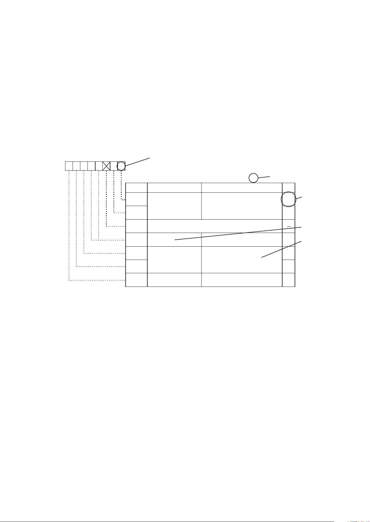
2. Register Diagram
The symbols, and descriptions, used for bit function in each register are shown below.
XXX Register
b7 b6 b5 b4 b3 b2 b1 b0
00
Symbol
XXX
XXX
(b2)
(b4-b3)
*1
Symbol
XXX
Bit
0
1
-
-
Bit Name
XXX Bit
Nothing is assigned. When write, set to "0",
When read, its content is indeterminate.
Reserved Bit Set to "0"
Address
XXX
Function
b1b0
0 0: XXX
0 1: XXX
1 0: Do not set a value
1 1: XXX
After Reset
00h
*5
RW
RW
RW
WO
*2
*3
*4
XXX5
XXX
XXX
XXX Bit
6
7
XXX Bit
Function varies depending on
mode of operation
0: XXX
1: XXX
*1
Blank:Set to “0” or “1” according to the application
0 : Set to “0”
1 : Set to “1”
X : Nothing is assigned
*2
RW : Read and write
RO : Read only
WO: Write only
– : Nothing is assigned
*3
• Reserved bit
Reserved bit. Set to specified value.
*4
• Nothing is assigned
Nothing is assigned to the bit concerned. As the bit may be use for future functions, set to “0” when
writing to this bit.
• Do not set to this value
The operation is not guaranteed when a value is set.
• Function varies depending on mode of operation
Bit function varies depending on peripheral function mode.
Refer to respective register for each mode.
*5
Follow the text in each manual for binary and hexadecimal notations.
RW
RW
RO
Page 4

3. M16C Family Documents
The following documents were prepared for the M16C family
Document Contents
Short Sheet Hardware overview
Data Sheet Hardware overview and electrical characteristics
Hardware Manual Hardware specifications (pin assignments, memory maps, peripheral
specifications, electrical characteristics, timing charts)
Software Manual Detailed description of assembly instructions and microcomputer
performance of each instruction
Application Note • Application examples of peripheral functions
• Sample programs
• Introduction to the basic functions in the M16C family
• Programming method with Assembly and C languages
RENESAS TECHNICAL UPDATE
Preliminary report about the specification of a product, a document, etc.
NOTE:
1. Before using this material , please visit our website to verify that this is the most updated document
available.
(1)
.
Page 5

Table of Contents
SFR Page Reference ............................................................................................................ B-1
1. Overview ............................................................................................................................... 1
1.1 Applications ..................................................................................................................................................1
1.2 Performance Outline ....................................................................................................................................2
1.3 Block Diagram .............................................................................................................................................. 4
1.4 Product List ..................................................................................................................................................5
1.5 Pin Configuration .........................................................................................................................................6
1.6 Pin Description ............................................................................................................................................. 8
2. Central Processing Unit (CPU) ........................................................................................... 10
2.1 Data Registers (R0, R1, R2, and R3) ........................................................................................................ 10
2.2 Address Registers (A0 and A1) .................................................................................................................. 10
2.3 Frame Base Register (FB) ......................................................................................................................... 11
2.4 Interrupt Table Register (INTB) .................................................................................................................. 11
2.5 Program Counter (PC) ............................................................................................................................... 11
2.6 User Stack Pointer (USP), Interrupt Stack Pointer (ISP) ........................................................................... 11
2.7 Static Base Register (SB) .......................................................................................................................... 11
2.8 Flag Register (FLG) ................................................................................................................................... 11
2.8.1 Carry Flag (C Flag) ............................................................................................................................ 11
2.8.2 Debug Flag (D Flag) .......................................................................................................................... 11
2.8.3 Zero Flag (Z Flag) .............................................................................................................................. 11
2.8.4 Sign Flag (S Flag) .............................................................................................................................. 11
2.8.5 Register Bank Select Flag (B Flag).................................................................................................... 11
2.8.6 Overflow Flag (O Flag)....................................................................................................................... 11
2.8.7 Interrupt Enable Flag (I Flag) ............................................................................................................. 11
2.8.8 Stack Pointer Select Flag (U Flag)..................................................................................................... 11
2.8.9 Processor Interrupt Priority Level (IPL) .............................................................................................. 11
2.8.10 Reserved Area ................................................................................................................................. 11
3. Memory ............................................................................................................................... 12
4. Special Function Register (SFR)......................................................................................... 13
5. Reset ................................................................................................................................... 25
5.1 Hardware Reset .........................................................................................................................................25
5.1.1 Reset on a Stable Supply Voltage ..................................................................................................... 25
5.1.2 Power-on Reset ................................................................................................................................. 25
5.2 Software Reset ..........................................................................................................................................25
5.3 Watchdog Timer Reset ............................................................................................................................... 25
5.4 Oscillation Stop Detection Reset ............................................................................................................... 25
6. Processor Mode ..................................................................................................................28
7. Clock Generating Circuit .....................................................................................................31
7.1 Types of Clock Generating Circuit ............................................................................................................. 31
7.1.1 Main Clock ......................................................................................................................................... 39
7.1.2 Sub Clock........................................................................................................................................... 40
7.1.3 On-chip Oscillator Clock .................................................................................................................... 41
7.1.4 PLL Clock ........................................................................................................................................... 41
A-1
Page 6

7.2 CPU Clock and Peripheral Function Clock ................................................................................................ 43
7.2.1 CPU Clock and BCLK ........................................................................................................................43
7.2.2 Peripheral Function Clock .................................................................................................................. 43
7.3 Clock Output Function ............................................................................................................................... 43
7.4 Power Control ............................................................................................................................................ 44
7.4.1 Normal Operation Mode..................................................................................................................... 44
7.4.2 Wait Mode .......................................................................................................................................... 46
7.4.3 Stop Mode.......................................................................................................................................... 48
7.5 Oscillation Stop and Re-oscillation Detection Function ............................................................................. 53
7.5.1 Operation When CM27 Bit = 0 (Oscillation Stop Detection Reset) .................................................... 53
7.5.2 Operation When CM27 Bit = 1 (Oscillation Stop, Re-oscillation Detection Interrupt) ........................ 53
7.5.3 How to Use Oscillation Stop and Re-oscillation Detection Function .................................................. 54
8. Protection ............................................................................................................................55
9. Interrupt ............................................................................................................................... 56
9.1 Type of Interrupts ....................................................................................................................................... 56
9.2 Software Interrupts ..................................................................................................................................... 57
9.2.1 Undefined Instruction Interrupt........................................................................................................... 57
9.2.2 Overflow Interrupt .............................................................................................................................. 57
9.2.3 BRK Interrupt ..................................................................................................................................... 57
9.2.4 INT Instruction Interrupt ..................................................................................................................... 57
9.3 Hardware Interrupts ................................................................................................................................... 58
9.3.1 Special Interrupts ...............................................................................................................................58
9.3.2 Peripheral Function Interrupts............................................................................................................ 58
9.4 Interrupts and Interrupt Vector ...................................................................................................................59
9.4.1 Fixed Vector Tables ............................................................................................................................ 59
9.4.2 Relocatable Vector Tables .................................................................................................................59
9.5 Interrupt Control .........................................................................................................................................61
9.5.1 I Flag ..................................................................................................................................................63
9.5.2 IR Bit .................................................................................................................................................. 63
9.5.3 ILVL2 to ILVL0 Bits and IPL ............................................................................................................... 63
9.5.4 Interrupt Sequence ............................................................................................................................ 64
9.5.5 Interrupt Response Time.................................................................................................................... 65
9.5.6 Variation of IPL when Interrupt Request is Accepted ......................................................................... 65
9.5.7 Saving Registers ................................................................................................................................ 66
9.5.8 Returning from an Interrupt Routine .................................................................................................. 67
9.5.9 Interrupt Priority ................................................................................................................................. 67
9.5.10 Interrupt Priority Resolution Circuit .................................................................................................. 67
______
9.6 INT Interrupt ...............................................................................................................................................69
______
9.7 NMI Interrupt ..............................................................................................................................................73
9.8 Key Input Interrupt .....................................................................................................................................73
9.9 CAN0 Wake-up Interrupt ............................................................................................................................ 73
9.10 Address Match Interrupt ........................................................................................................................... 74
10. Watchdog Timer ................................................................................................................ 76
10.1 Count Source Protective Mode ................................................................................................................77
A-2
Page 7

11. DMAC ................................................................................................................................ 78
11.1 Transfer Cycle .......................................................................................................................................... 83
11.1.1 Effect of Source and Destination Addresses .................................................................................... 83
11.1.2 Effect of Software Wait ..................................................................................................................... 83
11.2 DMA Transfer Cycles ................................................................................................................................ 85
11.3 DMA Enable ............................................................................................................................................. 86
11.4 DMA Request ...........................................................................................................................................86
11.5 Channel Priority and DMA Transfer Timing ..............................................................................................87
12. Timers ............................................................................................................................... 88
12.1 Timer A .....................................................................................................................................................90
12.1.1 Timer Mode ......................................................................................................................................94
12.1.2 Event Counter Mode ........................................................................................................................95
12.1.3 One-shot Timer Mode ....................................................................................................................100
12.1.4 Pulse Width Modulation (PWM) Mode ...........................................................................................102
12.2 Timer B................................................................................................................................................... 105
12.2.1 Timer Mode ....................................................................................................................................108
12.2.2 Event Counter Mode ......................................................................................................................109
12.2.3 Pulse Period and Pulse Width Measurement Mode ...................................................................... 110
13. Three-Phase Motor Control Timer Function .................................................................... 113
14. Serial I/O ......................................................................................................................... 124
14.1 UARTi.....................................................................................................................................................124
14.1.1 Clock Synchronous Serial I/O Mode ..............................................................................................134
14.1.2 Clock Asynchronous Serial I/O (UART) Mode ...............................................................................142
14.1.3 Special Mode 1 (I2C Mode) ............................................................................................................150
14.1.4 Special Mode 2 .............................................................................................................................. 159
14.1.5 Special Mode 3 (IE Mode) ............................................................................................................. 164
14.1.6 Special Mode 4 (SIM Mode) (UART2) ........................................................................................... 166
14.2 SI/Oi .......................................................................................................................................................171
14.2.1 SI/Oi Operation Timing................................................................................................................... 175
14.2.2 CLK Polarity Selection ................................................................................................................... 175
14.2.3 Functions for Setting an SOUTi Initial Value .................................................................................. 176
15. A/D Converter ..................................................................................................................177
15.1 Mode Description ...................................................................................................................................181
15.1.1 One-shot Mode .............................................................................................................................. 181
15.1.2 Repeat Mode ................................................................................................................................. 183
15.1.3 Single Sweep Mode .......................................................................................................................185
15.1.4 Repeat Sweep Mode 0 .................................................................................................................. 187
15.1.5 Repeat Sweep Mode 1 .................................................................................................................. 189
15.2 Function ................................................................................................................................................. 191
15.2.1 Resolution Select Function ............................................................................................................ 191
15.2.2 Sample and Hold ........................................................................................................................... 191
15.2.3 Extended Analog Input Pins........................................................................................................... 191
15.2.4 External Operation Amplifier (Op-Amp) Connection Mode ............................................................191
15.2.5 Current Consumption Reducing Function ...................................................................................... 192
15.2.6 Output Impedance of Sensor under A/D Conversion..................................................................... 192
16. D/A Converter.................................................................................................................. 194
17. CRC Calculation.............................................................................................................. 196
A-3
Page 8

18. CAN Module .................................................................................................................... 198
18.1 CAN Module-Related Registers ............................................................................................................. 199
18.1.1 CAN Message Box......................................................................................................................... 199
18.1.2 Acceptance Mask Registers........................................................................................................... 199
18.1.3 CAN SFR Registers .......................................................................................................................199
18.2 CAN0 Message Box ............................................................................................................................... 200
18.3 Acceptance Mask Registers...................................................................................................................202
18.4 CAN SFR Registers ...............................................................................................................................203
18.5 Operational Modes ................................................................................................................................. 210
18.5.1 CAN Reset/Initialization Mode ....................................................................................................... 210
18.5.2 CAN Operation Mode..................................................................................................................... 211
18.5.3 CAN Sleep Mode ........................................................................................................................... 211
18.5.4 CAN Interface Sleep Mode ............................................................................................................ 211
18.5.5 Bus Off State.................................................................................................................................. 212
18.6 Configuration CAN Module System Clock ............................................................................................. 213
18.7 Bit Timing Configuration ......................................................................................................................... 213
18.8 Bit-rate ................................................................................................................................................... 214
18.9 Acceptance Filtering Function and Masking Function............................................................................215
18.10 Acceptance Filter Support Unit (ASU)..................................................................................................216
18.11 Basic CAN Mode ..................................................................................................................................217
18.12 Return from Bus off Function ...............................................................................................................218
18.13 Time Stamp Counter and Time Stamp Function ..................................................................................218
18.14 Listen-Only Mode ................................................................................................................................. 218
18.15 Reception and Transmission................................................................................................................219
18.15.1 Reception ..................................................................................................................................... 220
18.15.2 Transmission ................................................................................................................................ 221
18.16 CAN Interrupt .......................................................................................................................................222
19. Programmable I/O Ports ................................................................................................. 223
19.1 PDi Register ........................................................................................................................................... 224
19.2 Pi Register, PC14 Register ....................................................................................................................224
19.3 PURj Register ........................................................................................................................................ 224
19.4 PCR Register .........................................................................................................................................224
20. Flash Memory Version .................................................................................................... 235
20.1 Memory Map ..........................................................................................................................................236
20.1.1 Boot Mode...................................................................................................................................... 237
20.2 Functions to Prevent Flash Memory from Rewriting .............................................................................. 237
20.2.1 ROM Code Protect Function .......................................................................................................... 237
20.2.2 ID Code Check Function ................................................................................................................ 237
20.3 CPU Rewrite Mode ................................................................................................................................ 239
20.3.1 EW0 Mode ..................................................................................................................................... 240
20.3.2 EW1 Mode ..................................................................................................................................... 240
20.3.3 FMR0, FMR1 Registers ................................................................................................................. 241
20.3.4 Precautions on CPU Rewrite Mode ............................................................................................... 245
20.3.5 Software Commands ..................................................................................................................... 247
20.3.6 Data Protect Function .................................................................................................................... 252
20.3.7 Status Register (SRD Register) .....................................................................................................252
20.3.8 Full Status Check ........................................................................................................................... 254
A-4
Page 9

20.4 Standard Serial I/O Mode ...................................................................................................................... 256
20.4.1 ID Code Check Function ................................................................................................................ 256
20.4.2 Example of Circuit Application in Standard Serial I/O Mode .......................................................... 260
20.5 Parallel I/O Mode ................................................................................................................................... 261
20.5.1 User ROM and Boot ROM Areas ................................................................................................... 261
20.5.2 ROM Code Protect Function .......................................................................................................... 261
20.6 CAN I/O Mode ........................................................................................................................................ 262
20.6.1 ID Code Check Function ................................................................................................................ 262
20.6.2 Example of Circuit Application in CAN I/O Mode ...........................................................................265
21. Electrical Characteristics ................................................................................................. 266
22. Usage Precaution............................................................................................................ 276
22.1 SFR ........................................................................................................................................................ 276
22.2 External Clock ........................................................................................................................................ 277
22.3 PLL Frequency Synthesizer ...................................................................................................................278
22.4 Power Control ........................................................................................................................................ 279
22.5 Oscillation Stop, Re-oscillation Detection Function ............................................................................... 281
22.6 Protection ............................................................................................................................................... 282
22.7 Interrupt .................................................................................................................................................. 283
22.7.1 Reading Address 00000h............................................................................................................... 283
22.7.2 Setting SP ......................................................................................................................................283
_______
22.7.3 NMI Interrupt ..................................................................................................................................283
22.7.4 Changing Interrupt Generate Factor ..............................................................................................284
22.7.5 INT Interrupt ................................................................................................................................... 284
22.7.6 Rewrite Interrupt Control Register ................................................................................................. 285
22.7.7 Watchdog Timer Interrupt .............................................................................................................. 285
22.8 DMAC .................................................................................................................................................... 286
22.8.1 Write to DMAE Bit in DMiCON Register ........................................................................................ 286
22.9 Timers .................................................................................................................................................... 287
22.9.1 Timer A........................................................................................................................................... 287
22.9.2 Timer B........................................................................................................................................... 291
22.10 Thee-Phase Motor Control Timer Function .......................................................................................... 293
22.11 Serial I/O ..............................................................................................................................................294
22.11.1 Clock Synchronous Serial I/O Mode ............................................................................................ 294
22.11.2 Special Modes .............................................................................................................................. 295
22.11.3 SI/Oi ............................................................................................................................................. 296
22.12 A/D Converter ...................................................................................................................................... 297
22.13 CAN Module ......................................................................................................................................... 299
22.13.1 Reading C0STR Register ............................................................................................................ 299
22.13.2 Performing CAN Configuration .................................................................................................... 301
22.13.3 Suggestions to Reduce Power Consumption .............................................................................. 302
22.13.4 CAN Transceiver in Boot Mode.................................................................................................... 303
22.14 Programmable I/O Ports ...................................................................................................................... 304
22.15 Dedicated Input Pin .............................................................................................................................. 305
22.16 Electrical Characteristic Differences Between Mask ROM and Flash Memory Version Microcomputers ..... 306
22.17 Mask ROM Version ............................................................................................................................. 307
_____
A-5
Page 10

22.18 Flash Memory Version .........................................................................................................................308
22.18.1 Functions to Prevent Flash Memory from Rewriting ....................................................................308
22.18.2 Stop Mode.................................................................................................................................... 308
22.18.3 Wait Mode .................................................................................................................................... 308
22.18.4 Low Power Dissipation Mode and On-Chip Oscillator Low Power Dissipation Mode ................. 308
22.18.5 Writing Command and Data......................................................................................................... 308
22.18.6 Program Command...................................................................................................................... 308
22.18.7 Lock Bit Program Command ........................................................................................................ 308
22.18.8 Operation Speed .......................................................................................................................... 309
22.18.9 Prohibited Instructions ................................................................................................................. 309
22.18.10 Interrupt...................................................................................................................................... 309
22.18.11 How to Access............................................................................................................................ 309
22.18.12 Rewriting in User ROM Area...................................................................................................... 309
22.18.13 DMA Transfer .............................................................................................................................309
22.19 Flash Memory Programming Using Boot Program .............................................................................. 310
22.19.1 Programming Using Serial I/O Mode ........................................................................................... 310
22.19.2 Programming Using CAN I/O Mode ............................................................................................. 310
22.20 Noise .................................................................................................................................................... 311
Appendix 1. Package Dimensions ........................................................................................ 312
Register Index .......................................................................................................................313
Specifications written in this manual are believed to be accurate, but are not guaranteed to be entirely free
of error. Specifications in this manual may be changed for functional or performance improvements.
Please make sure your manual is the latest edition.
A-6
Page 11
SFR Page Reference
C01WKIC
C0RECIC
C0TRMIC
INT3IC
TB5IC
S5IC
TB4IC
U1BCNIC
TB3IC
U0BCNIC
S4IC
INT5IC
S3IC
INT4IC
U2BCNIC
DM0IC
DM1IC
C01ERRIC
ADIC
KUPIC
S2TIC
S2RIC
S0TIC
S0RIC
S1TIC
S1RIC
TA0IC
TA1IC
TA2IC
INT7IC
TA3IC
INT6IC
TA4IC
TB0IC
S6IC
TB1IC
INT8IC
TB2IC
INT0IC
INT1IC
INT2IC
Address Register Symbol Page
0040h
0041h
0042h
0043h
0044h
0045h
0046h
0047h
0048h
0049h
004Ah
004Bh
004Ch
004Dh
004Eh
004Fh
0050h
0051h
0052h
0053h
0054h
0055h
0056h
0057h
0058h
0059h
005Ah
005Bh
005Ch
005Dh
005Eh
005Fh
0060h
0061h
0062h
0063h
0064h
0065h
0066h
0067h
0068h
0069h
006Ah
006Bh
006Ch
006Dh
006Eh
006Fh
0070h
0071h
0072h
0073h
0074h
0075h
0076h
0077h
0078h
0079h
007Ah
007Bh
007Ch
007Dh
007Eh
007Fh
61
61
61
62
61
61
61
61
61
61
62
62
62
62
61
61
61
61
61
61
61
61
61
61
61
61
61
61
62
62
62
62
61
61
61
62
62
61
62
62
62
200
201
CAN0 Wake-up Interrupt Control Register
CAN0 Successful Reception Interrupt Control Register
CAN0 Successful Transmission Interrupt Control Register
INT3 Interrupt Control Register
Timer B5 Interrupt Control Register
SI/O5 Interrupt Control Register
Timer B4 Interrupt Control Register
UART1 Bus Collision Detection Interrupt Control Register
Timer B3 Interrupt Control Register
UART0 Bus Collision Detection Interrupt Control Register
SI/O4 Interrupt Control Register
INT5 Interrupt Control Register
SI/O3 Interrupt Control Register
INT4 Interrupt Control Register
UART2 Bus Collision Detection Interrupt Control Register
DMA0 Interrupt Control Register
DMA1 Interrupt Control Register
CAN0 Error Interrupt Control Register
A/D Conversion Interrupt Control Register
Key Input Interrupt Control Register
UART2 Transmit Interrupt Control Register
UART2 Receive Interrupt Control Register
UART0 Transmit Interrupt Control Register
UART0 Receive Interrupt Control Register
UART1 Transmit Interrupt Control Register
UART1 Receive Interrupt Control Register
Timer A0 Interrupt Control Register
Timer A1 Interrupt Control Register
Timer A2 Interrupt Control Register
INT7 Interrupt Control Register
Timer A3 Interrupt Control Register
INT6 Interrupt Control Register
Timer A4 Interrupt Control Register
Timer B0 Interrupt Control Register
SI/O6 Interrupt Control Register
Timer B1 Interrupt Control Register
INT8 Interrupt Control Register
Timer B2 Interrupt Control Register
INT0 Interrupt Control Register
INT1 Interrupt Control Register
INT2 Interrupt Control Register
CAN0 Message Box 0: Identifier / DLC
CAN0 Message Box 0: Data Field
CAN0 Message Box 0: Time Stamp
CAN0 Message Box 1: Identifier / DLC
CAN0 Message Box 1: Data Field
CAN0 Message Box 1: Time Stamp
Address Register Symbol Page
0000h
0001h
0002h
0003h
Processor Mode Register 0
0004h
Processor Mode Register 1
0005h
System Clock Control Register 0
0006h
0007h
The blank areas are reserved.
System Clock Control Register 1
0008h
0009h
Address Match Interrupt Enable Register
000Ah
Protect Register
000Bh
000Ch
Oscillation Stop Detection Register
000Dh
000Eh
Watchdog Timer Start Register
000Fh
Watchdog Timer Control Register
0010h
0011h
Address Match Interrupt Register 0
0012h
0013h
0014h
0015h
Address Match Interrupt Register 1
0016h
0017h
0018h
0019h
001Ah
001Bh
001Ch
PLL Control Register 0
001Dh
001Eh
Processor Mode Register 2
001Fh
0020h
0021h
DMA0 Source Pointer
0022h
0023h
0024h
0025h
DMA0 Destination Pointer
0026h
0027h
0028h
DMA0 Transfer Counter
0029h
002Ah
002Bh
002Ch
DMA0 Control Register
002Dh
002Eh
002Fh
0030h
0031h
DMA1 Source Pointer
0032h
0033h
0034h
0035h
DMA1 Destination Pointer
0036h
0037h
0038h
DMA1 Transfer Counter
0039h
003Ah
003Bh
003Ch
DMA1 Control Register
003Dh
003Eh
003Fh
PM0
PM1
CM0
CM1
AIER
PRCR
CM2
WDTS
WDC
RMAD0
RMAD1
PLC0
PM2
SAR0
DAR0
TCR0
DM0CON
SAR1
DAR1
TCR1
DM1CON
28
29
33
34
75
55
35
77
77
75
75
38
37
82
82
82
81
82
82
82
81
B-1
Page 12
Address Register Symbol Page
Address Register Symbol Page
00C0h
00C1h
00C2h
00C3h
00C4h
00C5h
00C6h
00C7h
00C8h
00C9h
00CAh
00CBh
00CCh
00CDh
00CEh
00CFh
00D0h
00D1h
00D2h
00D3h
00D4h
00D5h
00D6h
00D7h
00D8h
00D9h
00DAh
00DBh
00DCh
00DDh
00DEh
00DFh
00E0h
00E1h
00E2h
00E3h
00E4h
00E5h
00E6h
00E7h
00E8h
00E9h
00EAh
00EBh
00ECh
00EDh
00EEh
00EFh
00F0h
00F1h
00F2h
00F3h
00F4h
00F5h
00F6h
00F7h
00F8h
00F9h
00FAh
00FBh
00FCh
00FDh
00FEh
00FFh
200
201
CAN0 Message Box 6: Identifier / DLC
CAN0 Message Box 6: Data Field
CAN0 Message Box 6: Time Stamp
CAN0 Message Box 7: Identifier / DLC
CAN0 Message Box 7: Data Field
CAN0 Message Box 7: Time Stamp
CAN0 Message Box 8: Identifier / DLC
CAN0 Message Box 8: Data Field
CAN0 Message Box 8: Time Stamp
CAN0 Message Box 9: Identifier / DLC
CAN0 Message Box 9: Data Field
CAN0 Message Box 9: Time Stamp
0080h
0081h
0082h
CAN0 Message Box 2: Identifier / DLC
0083h
0084h
0085h
0086h
0087h
0088h
0089h
CAN0 Message Box 2: Data Field
008Ah
008Bh
008Ch
008Dh
008Eh
CAN0 Message Box 2: Time Stamp
008Fh
0090h
0091h
0092h
CAN0 Message Box 3: Identifier / DLC
0093h
0094h
0095h
0096h
0097h
0098h
0099h
CAN0 Message Box 3: Data Field
009Ah
009Bh
009Ch
009Dh
009Eh
CAN0 Message Box 3: Time Stamp
009Fh
00A0h
00A1h
00A2h
CAN0 Message Box 4: Identifier / DLC
00A3h
00A4h
00A5h
00A6h
00A7h
00A8h
00A9h
CAN0 Message Box 4: Data Field
00AAh
00ABh
00ACh
00ADh
00AEh
CAN0 Message Box 4: Time Stamp
00AFh
00B0h
00B1h
00B2h
CAN0 Message Box 5: Identifier / DLC
00B3h
00B4h
00B5h
00B6h
00B7h
00B8h
00B9h
CAN0 Message Box 5: Data Field
00BAh
00BBh
00BCh
00BDh
00BEh
CAN0 Message Box 5: Time Stamp
00BFh
200
201
B-2
Page 13
Address Register Symbol Page
C0GMR
C0LMAR
C0LMBR
Address Register Symbol Page
0140h
0141h
0142h
0143h
0144h
0145h
0146h
0147h
0148h
0149h
014Ah
014Bh
014Ch
014Dh
014Eh
014Fh
0150h
0151h
0152h
0153h
0154h
0155h
0156h
0157h
0158h
0159h
015Ah
015Bh
015Ch
015Dh
015Eh
015Fh
0160h
0161h
0162h
0163h
0164h
0165h
0166h
0167h
0168h
0169h
016Ah
016Bh
016Ch
016Dh
016Eh
016Fh
0170h
0171h
0172h
0173h
0174h
0175h
0176h
0177h
0178h
0179h
017Ah
017Bh
017Ch
017Dh
017Eh
017Fh
200
201
202
202
202
CAN0 Message Box 14: Identifier /DLC
CAN0 Message Box 14: Data Field
CAN0 Message Box 14: Time Stamp
CAN0 Message Box 15: Identifier /DLC
CAN0 Message Box 15: Data Field
CAN0 Message Box 15: Time Stamp
CAN0 Global Mask Register
CAN0 Local Mask A Register
CAN0 Local Mask B Register
0100h
0101h
0102h
CAN0 Message Box 10: Identifier / DLC
0103h
0104h
0105h
0106h
0107h
0108h
0109h
CAN0 Message Box 10: Data Field
010Ah
010Bh
010Ch
010Dh
010Eh
CAN0 Message Box 10: Time Stamp
010Fh
0110h
0111 h
0112h
CAN0 Message Box 11: Identifier / DLC
0113h
0114h
0115h
0116h
0117h
0118h
0119h
CAN0 Message Box 11: Data Field
011Ah
011Bh
011Ch
011Dh
011Eh
CAN0 Message Box 11: Time Stamp
011Fh
0120h
0121h
0122h
CAN0 Message Box 12: Identifier / DLC
0123h
0124h
0125h
0126h
0127h
0128h
0129h
CAN0 Message Box 12: Data Field
012Ah
012Bh
012Ch
012Dh
012Eh
CAN0 Message Box 12: Time Stamp
012Fh
0130h
0131h
0132h
The blank areas are reserved.
CAN0 Message Box 13: Identifier / DLC
0133h
0134h
0135h
0136h
0137h
0138h
0139h
CAN0 Message Box 13: Data Field
013Ah
013Bh
013Ch
013Dh
013Eh
CAN0 Message Box 13: Time Stamp
013Fh
200
201
B-3
Page 14
Address Register Symbol Page
TBSR
TA11
TA21
TA41
INVC0
INVC1
IDB0
IDB1
DTT
ICTB2
IFSR2
TB3
TB4
TB5
S6TRR
S6C
S6BRG
S3456TRR
TB3MR
TB4MR
TB5MR
IFSR0
IFSR1
S3TRR
S3C
S3BRG
S4TRR
S4C
S4BRG
S5TRR
S5C
S5BRG
U0SMR4
U0SMR3
U0SMR2
U0SMR
U1SMR4
U1SMR3
U1SMR2
U1SMR
U2SMR4
U2SMR3
U2SMR2
U2SMR
U2MR
U2BRG
U2TB
U2C0
U2C1
U2RB
Address Register Symbol Page
01C0h
01C1h
01C2h
01C3h
01C4h
01C5h
01C6h
01C7h
01C8h
01C9h
01CAh
01CBh
01CCh
01CDh
01CEh
01CFh
01D0h
01D1h
01D2h
01D3h
01D4h
01D5h
01D6h
01D7h
01D8h
01D9h
01DAh
01DBh
01DCh
01DDh
01DEh
01DFh
01E0h
01E1h
01E2h
01E3h
01E4h
01E5h
01E6h
01E7h
01E8h
01E9h
01EAh
01EBh
01ECh
01EDh
01EEh
01EFh
01F0h
01F1h
01F2h
01F3h
01F4h
01F5h
01F6h
01F7h
01F8h
01F9h
01FAh
01FBh
01FCh
01FDh
01FEh
01FFh
107
118
118
118
115
116
117
117
117
119
72
116
106
106
172
172
172
173
106
108
109
111
70
71
172
172
172
172
172
172
172
172
172
133
132
132
131
133
132
132
131
133
132
132
131
129
128
128
129
130
128
Timer B3, B4, B5 Count Start Flag
Timer A1-1 Register
Timer A2-1 Register
Timer A4-1 Register
Three-Phase PWM Control Register 0
Three-Phase PWM Control Register 1
Three-Phase Output Buffer Register 0
Three-Phase Output Buffer Register 1
Dead Time Timer
Timer B2 Interrupt Occurrence Frequency Set Counter
Interrupt Cause Select Register 2
Timer B3 Register
Timer B4 Register
Timer B5 Register
SI/O6 Transmit/Receive Register
SI/O6 Control Register
SI/O6 Bit Rate Generator
SI/O3, 4, 5, 6 Transmit/Receive Register
Timer B3 Mode Register
Timer B4 Mode Register
Timer B5 Mode Register
Interrupt Cause Select Register 0
Interrupt Cause Select Register 1
SI/O3 Transmit/Receive Register
SI/O3 Control Register
SI/O3 Bit Rate Generator
SI/O4 Transmit/Receive Register
SI/O4 Control Register
SI/O4 Bit Rate Generator
SI/O5 Transmit/Receive Register
SI/O5 Control Register
SI/O5 Bit Rate Generator
UART0 Special Mode Register 4
UART0 Special Mode Register 3
UART0 Special Mode Register 2
UART0 Special Mode Register
UART1 Special Mode Register 4
UART1 Special Mode Register 3
UART1 Special Mode Register 2
UART1 Special Mode Register
UART2 Special Mode Register 4
UART2 Special Mode Register 3
UART2 Special Mode Register 2
UART2 Special Mode Register
UART2 Transmit/Receive Mode Register
UART2 Bit Rate Generator
UART2 Transmit Buffer Register
UART2 Transmit/Receive Control Register 0
UART2 Transmit/Receive Control Register 1
UART2 Receive Buffer Register
0180h
0181h
0182h
0183h
0184h
0185h
0186h
0187h
0188h
0189h
018Ah
018Bh
018Ch
018Dh
018Eh
018Fh
0190h
0191h
0192h
0193h
0194h
0195h
0196h
0197h
0198h
0199h
019Ah
019Bh
019Ch
019Dh
019Eh
019Fh
01A0h
01A1h
01A2h
01A3h
01A4h
01A5h
01A6h
01A7h
01A8h
01A9h
01AAh
01ABh
01ACh
01ADh
01AEh
01AFh
01B0h
01B1h
01B2h
01B3h
01B4h
01B5h
The blank areas are reserved.
Flash Memory Control Register 1
01B6h
01B7h
Flash Memory Control Register 0
01B8h
01B9h
Address Match Interrupt Register 2
01BAh
01BBh
Address Match Interrupt Enable Register 2
01BCh
01BDh
Address Match Interrupt Register 3
01BEh
01BFh
FMR1
FMR0
RMAD2
AIER2
RMAD3
241
241
75
75
75
B-4
Page 15
Address Register Symbol Page
Address Register Symbol Page
C0AFS
PCLKR
CCLKR
0240h
0241h
0242h
0243h
0244h
0245h
0246h
0247h
0248h
0249h
024Ah
024Bh
024Ch
024Dh
024Eh
024Fh
0250h
0251h
0252h
0253h
0254h
0255h
0256h
0257h
0258h
0259h
025Ah
025Bh
025Ch
025Dh
025Eh
025Fh
0260h
0261h
0262h
0263h
0264h
0265h
0266h
0267h
0268h
0269h
026Ah
026Bh
026Ch
026Dh
026Eh
026Fh
0270h
to
0372h
0373h
0374h
0375h
0376h
0377h
0378h
0379h
037Ah
037Bh
037Ch
037Dh
037Eh
037Fh
209
36
37
CAN0 Acceptance Filter Support Register
Peripheral Clock Select Register
CAN0 Clock Select Register
0200h
CAN0 Message Control Register 0
CAN0 Message Control Register 1
0201h
CAN0 Message Control Register 2
0202h
0203h
CAN0 Message Control Register 3
0204h
CAN0 Message Control Register 4
0205h
CAN0 Message Control Register 5
0206h
CAN0 Message Control Register 6
0207h
CAN0 Message Control Register 7
0208h
The blank areas are reserved.
CAN0 Message Control Register 8
0209h
CAN0 Message Control Register 9
020Ah
CAN0 Message Control Register 10
020Bh
CAN0 Message Control Register 11
020Ch
CAN0 Message Control Register 12
020Dh
CAN0 Message Control Register 13
020Eh
CAN0 Message Control Register 14
020Fh
CAN0 Message Control Register 15
0210h
CAN0 Control Register
0211h
0212h
CAN0 Status Register
0213h
0214h
CAN0 Slot Status Register
0215h
0216h
CAN0 Interrupt Control Register
0217h
0218h
CAN0 Extended ID Register
0219h
021Ah
CAN0 Configuration Register
021Bh
021Ch
CAN0 Receive Error Count Register
021Dh
CAN0 Transmit Error Count Register
021Eh
CAN0 Time Stamp Register
021Fh
0220h
0221h
0222h
0223h
0224h
0225h
0226h
0227h
0228h
0229h
022Ah
022Bh
022Ch
022Dh
022Eh
022Fh
0230h
CAN1 Control Register
0231h
0232h
0233h
0234h
0235h
0236h
0237h
0238h
0239h
023Ah
023Bh
023Ch
023Dh
023Eh
023Fh
C0MCTL0
C0MCTL1
C0MCTL2
C0MCTL3
C0MCTL4
C0MCTL5
C0MCTL6
C0MCTL7
C0MCTL8
C0MCTL9
C0MCTL10
C0MCTL11
C0MCTL12
C0MCTL13
C0MCTL14
C0MCTL15
C0CTLR
C0STR
C0SSTR
C0ICR
C0IDR
C0CONR
C0RECR
C0TECR
C0TSR
C1CTLR
203
204
206
207
207
207
208
209
209
209
205
B-5
Page 16
Address Register Symbol Page
AD0
AD1
AD2
AD3
AD4
AD5
AD6
AD7
ADCON2
ADCON0
ADCON1
DA0
DA1
DACON
PC14
PUR3
P0
P1
PD0
PD1
P2
P3
PD2
PD3
P4
P5
PD4
PD5
P6
P7
PD6
PD7
P8
P9
PD8
PD9
P10
P11
PD10
PD11
P12
P13
PD12
PD13
PUR0
PUR1
PUR2
PCR
Address Register Symbol Page
03C0h
03C1h
03C2h
03C3h
03C4h
03C5h
03C6h
03C7h
03C8h
03C9h
03CAh
03CBh
03CCh
03CDh
03CEh
03CFh
03D0h
03D1h
03D2h
03D3h
03D4h
03D5h
03D6h
03D7h
03D8h
03D9h
03DAh
03DBh
03DCh
03DDh
03DEh
03DFh
03E0h
03E1h
03E2h
03E3h
03E4h
03E5h
03E6h
03E7h
03E8h
03E9h
03EAh
03EBh
03ECh
03EDh
03EEh
03EFh
03F0h
03F1h
03F2h
03F3h
03F4h
03F5h
03F6h
03F7h
03F8h
03F9h
03FAh
03FBh
03FCh
03FDh
03FEh
03FFh
180
180
179,182,184
186,188,190
195
195
195
231
233
231
231
230
230
231
231
230
230
231
231
230
230
231
231
230
230
231
231
230
230
231
231
230
230
231
231
230
230
232
232
232
233
A/D Register 0
A/D Register 1
A/D Register 2
A/D Register 3
A/D Register 4
A/D Register 5
A/D Register 6
A/D Register 7
A/D Control Register 2
A/D Control Register 0
A/D Control Register 1
D/A Register 0
D/A Register 1
D/A Control Register
Port P14 Control Register
Pull-Up Control Register 3
Port P0 Register
Port P1 Register
Port P0 Direction Register
Port P1 Direction Register
Port P2 Register
Port P3 Register
Port P2 Direction Register
Port P3 Direction Register
Port P4 Register
Port P5 Register
Port P4 Direction Register
Port P5 Direction Register
Port P6 Register
Port P7 Register
Port P6 Direction Register
Port P7 Direction Register
Port P8 Register
Port P9 Register
Port P8 Direction Register
Port P9 Direction Register
Port P10 Register
Port P11 Register
Port P10 Direction Register
Port P11 Direction Register
Port P12 Register
Port P13 Register
Port P12 Direction Register
Port P13 Direction Register
Pull-up Control Register 0
Pull-up Control Register 1
Pull-up Control Register 2
Port Control Register
0380h
Count Start Flag
0381h
Clock Prescaler Reset Flag
0382h
One-Shot Start Flag
0383h
Trigger Select Register
0384h
Up/Down Flag
0385h
0386h
Timer A0 Register
0387h
0388h
The blank areas are reserved.
Timer A1 Register
0389h
038Ah
Timer A2 Register
038Bh
038Ch
Timer A3 Register
038Dh
038Eh
Timer A4 Register
038Fh
0390h
Timer B0 Register
0391h
0392h
Timer B1 Register
0393h
0394h
Timer B2 Register
0395h
Timer A0 Mode Register
0396h
Timer A1 Mode Register
0397h
Timer A2 Mode Register
0398h
Timer A3 Mode Register
0399h
Timer A4 Mode Register
039Ah
Timer B0 Mode Register
039Bh
Timer B1 Mode Register
039Ch
Timer B2 Mode Register
039Dh
Timer B2 Special Mode Register
039Eh
039Fh
UART0 Transmit/Receive Mode Register
03A0h
UART0 Bit Rate Generator
03A1h
03A2h
UART0 Transmit Buffer Register
03A3h
UART0 Transmit/Receive Control Register 0
03A4h
UART0 Transmit/Receive Control Register 1
03A5h
03A6h
UART0 Receive Buffer Register
03A7h
03A8h
UART1 Transmit/Receive Mode Register
03A9h
UART1 Bit Rate Generator
03AAh
UART1 Transmit Buffer Register
03ABh
03ACh
UART1 Transmit/Receive Control Register 0
03ADh
UART1 Transmit/Receive Control Register 1
03AEh
UART1 Receive Buffer Register
03AFh
03B0h
UART Transmit/Receive Control Register 2
03B1h
03B2h
03B3h
03B4h
03B5h
03B6h
03B7h
03B8h
DMA0 Request Cause Select Register
03B9h
03BAh
DMA1 Request Cause Select Register
03BBh
03BCh
CRC Data Register
03BDh
03BEh
CRC Input Register
03BFh
TABSR
CPSRF
ONSF
TRGSR
UDF
TA0
TA1
TA2
TA3
TA4
TB0
TB1
TB2
TA0MR
TA1MR
TA2MR
TA3MR
TA4MR
TB0MR
TB1MR
TB2MR
TB2SC
U0MR
U0BRG
U0TB
U0C0
U0C1
U0RB
U1MR
U1BRG
U1TB
U1C0
U1C1
U1RB
UCON
DM0SL
DM1SL
CRCD
CRCIN
92,107,120
93,107
93
93,120
92
91
91
118
91
118
91
91
118
106
106
106
118
91
94
121
96
98,121
101
98
103
98,121
106,108
109,111
121
119
129
128
128
129
130
128
129
128
128
129
130
128
131
80
81
196
196
B-6
Page 17

M16C/6N Group (M16C/6NL, M16C/6NN)
Under development
This document is under development and its contents are subject to change
SINGLE-CHIP 16-BIT CMOS MICROCOMPUTER
1. Overview
The M16C/6N Group (M16C/6NL, M16C/6NN) of single-chip microcomputers are built using the
high-performance silicon gate CMOS process using an M16C/60 Series CPU core and are packaged in
100-pin and 128-pin plastic molded LQFP. These single-chip microcomputers operate using sophisticated
instructions featuring a high level of instruction efficiency. With 1 Mbyte of address space, they are capable
of executing instructions at high speed. Being equipped with one CAN (Controller Area Network) module in
M16C/6N Group (M16C/6NL, M16C/6NN), the microcomputer is suited to car audio and industrial control
systems. The CAN module complies with the 2.0B specification. In addition, this microcomputer contains a
multiplier and DMAC which combined with fast instruction processing capability, makes it suitable for control
of various OA and communication equipment which requires high-speed arithmetic/logic operations.
1.1 Applications
Car audio and industrial control systems, other
Rev.1.02
Jul 01, 2005
Rev.1.02 Jul 01, 2005 page 1 of 314
REJ09B0126-0102
Page 18
Under development
This document is under development and its contents are subject to change.
M16C/6N Group (M16C/6NL, M16C/6NN) 1. Overview
1.2 Performance Outline
Tables 1.1 and 1.2 list a performance outline of M16C/6N Group (M16C/6NL, M16C/6NN).
Table 1.1 Performance Outline of M16C/6N Group (100-pin Version: M16C/6NL)
Item Performance
CPU Number of Basic Instructions 91 instructions
Minimum Instruction Execution Time
Operation Mode Single-chip mode
Address Space 1 Mbyte
Memory Capacity See Table 1.3 Product List
Peripheral Port Input/Output: 87 pins, Input: 1 pin
Function Multifunction Timer Timer A: 16 bits ✕ 5 channels
Serial I/O 3 channels
A/D Converter 10-bit A/D converter: 1 circuit, 26 channels
D/A Converter 8 bits ✕ 2 channels
DMAC 2 channels
CRC Calculation Circuit CRC-CCITT
CAN Module 1 channel with 2.0B specification
Watchdog Timer 15 bits ✕ 1 channel (with prescaler)
Interrupt Internal: 30 sources, External: 9 sources
Clock Generating Circuit 4 circuits
Oscillation Stop Detection Main clock oscillation stop and re-oscillation detection function
Function
Electrical Supply Voltage VCC = 3.0 to 5.5V
Characteristics
Power Mask ROM 19mA (f(BCLK) = 24MHz, PLL operation, no division)
Consumption
Flash Memory
Mask ROM 3µA
Flash Memory
Flash Memory
Version
Program/Erase Supply Voltage
Program and Erase Endurance
I/O I/O Withstand Voltage 5.0V
Characteristics
Output Current 5mA
Operating Ambient Temperature -40 to 85°C
Device Configuration CMOS high performance silicon gate
Package 100-pin plastic mold LQFP
NOTES:
1. I2C-bus is a registered trademark of Koninklijke Philips Electronics N.V.
2. IEBus is a registered trademark of NEC Electronics Corporation.
41.7ns (f(BCLK) = 24MHz, 1/1 prescaler, without software wait)
Timer B: 16 bits ✕ 6 channels
Three-phase motor control circuit
Clock synchronous, UART, I2C-bus
(1)
, IEBus
(2)
2 channels
Clock synchronous
Software: 4 sources, Priority level: 7 levels
• Main clock oscillation circuit (*)
• Sub clock oscillation circuit (*)
• On-chip oscillator
• PLL frequency synthesizer
(*) Equipped with a built-in feedback resistor
(f(BCLK) = 24MHz, 1/1 prescaler, without software wait)
21mA (f(BCLK) = 24MHz, PLL operation, no division)
(f(BCLK) = 32kHz, Wait mode, Oscillation capacity Low)
0.8µA (Stop mode, Topr = 25°C)
3.3 ± 0.3V or 5.0 ± 0.5V
100 times
Rev.1.02 Jul 01, 2005 page 2 of 314
REJ09B0126-0102
Page 19
Under development
This document is under development and its contents are subject to change.
M16C/6N Group (M16C/6NL, M16C/6NN) 1. Overview
Table 1.2 Performance Outline of M16C/6N Group (128-pin Version: M16C/6NN)
Item Performance
CPU Number of Basic Instructions 91 instructions
Minimum Instruction Execution Time
41.7ns (f(BCLK) = 24MHz, 1/1 prescaler, without software wait)
Operation Mode Single-chip mode
Address Space 1 Mbyte
Memory Capacity See Table 1.3 Product List
Peripheral Port Input/Output: 113 pins, Input: 1 pin
Function Multifunction Timer Timer A: 16 bits ✕ 5 channels
Timer B: 16 bits ✕ 6 channels
Three-phase motor control circuit
Serial I/O 3 channels
Clock synchronous, UART, I2C-bus
(1)
, IEBus
(2)
4 channels
Clock synchronous
A/D Converter 10-bit A/D converter: 1 circuit, 26 channels
D/A Converter 8 bits ✕ 2 channels
DMAC 2 channels
CRC Calculation Circuit CRC-CCITT
CAN Module 1 channel with 2.0B specification
Watchdog Timer 15 bits ✕ 1 channel (with prescaler)
Interrupt Internal: 32 sources, External: 12 sources
Software: 4 sources, Priority level: 7 levels
Clock Generating Circuit 4 circuits
• Main clock oscillation circuit (*)
• Sub clock oscillation circuit (*)
• On-chip oscillator
• PLL frequency synthesizer
(*) Equipped with a built-in feedback resistor
Oscillation Stop Detection Main clock oscillation stop and re-oscillation detection function
Function
Electrical Supply Voltage VCC = 3.0 to 5.5V
Characteristics
(f(BCLK) = 24MHz, 1/1 prescaler, without software wait)
Power Mask ROM 19mA (f(BCLK) = 24MHz, PLL operation, no division)
Flash Memory
Version
Consumption
Program/Erase Supply Voltage
Program and Erase Endurance
Flash Memory
21mA (f(BCLK) = 24MHz, PLL operation, no division)
Mask ROM 3µA
Flash Memory
0.8µA (Stop mode, Topr = 25°C)
3.3 ± 0.3V or 5.0 ± 0.5V
100 times
(f(BCLK) = 32kHz, Wait mode, Oscillation capacity Low)
I/O I/O Withstand Voltage 5.0V
Characteristics
Output Current 5mA
Operating Ambient Temperature -40 to 85°C
Device Configuration CMOS high performance silicon gate
Package 128-pin plastic mold LQFP
NOTES:
1. I2C-bus is a registered trademark of Koninklijke Philips Electronics N.V.
2. IEBus is a registered trademark of NEC Electronics Corporation.
Rev.1.02 Jul 01, 2005 page 3 of 314
REJ09B0126-0102
Page 20
Under development
This document is under development and its contents are subject to change.
M16C/6N Group (M16C/6NL, M16C/6NN) 1. Overview
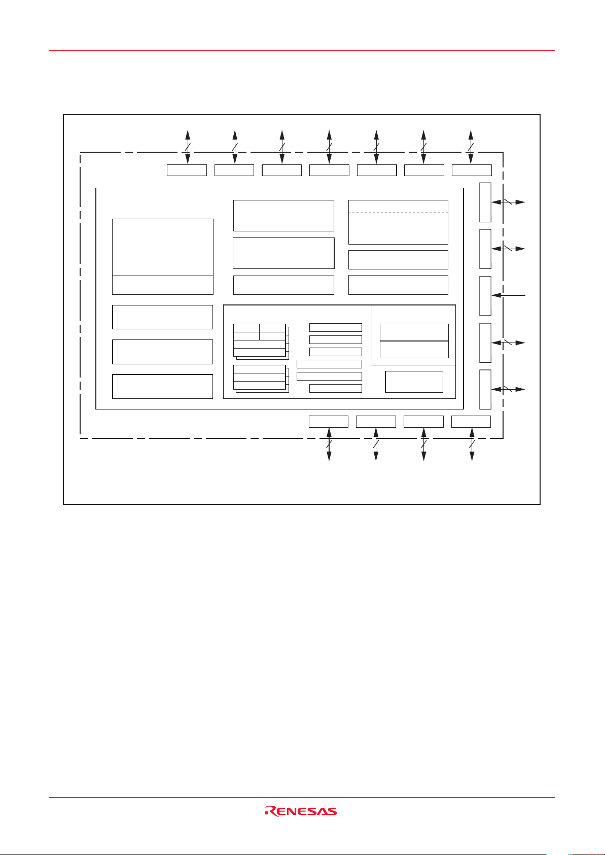
1.3 Block Diagram
Figure 1.1 shows a block diagram of M16C/6N Group (M16C/6NL, M16C/6NN).
8
Port P0
Port P18Port P2
Internal peripheral functions
Expandable up to 26 channels)
Timer (16 bits)
Output (timer A): 5
Input (timer B): 6
Three-phase motor
control circuit
Watchdog timer
(15 bits)
DMAC
(2 channels)
D/A converter
(8 bits ✕ 2 channels)
NOTES:
1: ROM size depends on microcomputer type.
2: RAM size depends on microcomputer type.
3: Ports P11 to P14 are only in the 128-pin version.
4: 8 bits ✕ 2 channels in the 100-pin version.
Clock synchronous serial I/O
CRC arithmetic circuit (CCITT)
8 8 8 8
A/D converter
(10 bits ✕ 8 channels
UART or
(3 channels)
(Polynomial: X
R0H R0L
R1H R1L
R2
R3
A0
A1
FB
16+X12+X5
+1)
SB
USP
ISP
INTB
PC
FLG
Port P14
(3)
2
Port P5Port P4Port P3
System clock generating circuit
XIN-XOUT
XCIN-XCOUT
PLL frequency synthesizer
On-chip oscillator
Clock synchronous serial I/O
(8 bits ✕ 4 channels)
CAN module
(1 channel)
(4)
MemoryM16C/60 series CPU core
(1)
ROM
(2)
RAM
Multiplier
Port P13
Port P12
(3)
8
(3)
8
8
Port P6
Port P7
8
Port P8
7
Port P8_5
Port P9
8
Port P10
8
Port P11
(3)
8
Figure 1.1 Block Diagram
Rev.1.02 Jul 01, 2005 page 4 of 314
REJ09B0126-0102
Page 21
Under development
This document is under development and its contents are subject to change.
M16C/6N Group (M16C/6NL, M16C/6NN) 1. Overview
1.4 Product List
Table 1.3 lists the M16C/6N Group (M16C/6NL, M16C/6NN) products and Figure 1.2 shows the type numbers,
memory sizes and packages.
Table 1.3 Product List
As of Jul. 2005
Type No. ROM Capacity RAM Capacity Package Type Remarks
M306NLFHGP 384 K + 4 Kbytes 31 Kbytes PLQP0100KB-A Flash memory
M306NNFHGP PLQP0128KB-A version
M306NLFJGP (D) 512 K + 4 Kbytes 31 Kbytes PLQP0100KB-A
M306NNFJGP PLQP0128KB-A
M306NLME-XXXGP 192 Kbytes 16 Kbytes PLQP0100KB-A Mask ROM version
M306NNME-XXXGP PLQP0128KB-A
M306NLMG-XXXGP 256 Kbytes 20 Kbytes PLQP0100KB-A
M306NNMG-XXXGP PLQP0128KB-A
(D): Under development
Type No.
M30 6N L M G - XXX GP
Package type:
GP: Package PLQP0100KB-A, PLQP0128KB-A
ROM No.
Omitted on flash memory version
ROM capacity:
E : 192 Kbytes
G: 256 Kbytes
H : 384 Kbytes
J : 512 Kbytes
Figure 1.2 Type No., Memory Size, and Package
Memory type:
M : Mask ROM version
F : Flash memory version
Shows the number of CAN module, pin count, etc.
6N Group
M16C Family
Rev.1.02 Jul 01, 2005 page 5 of 314
REJ09B0126-0102
Page 22
Under development
This document is under development and its contents are subject to change.
M16C/6N Group (M16C/6NL, M16C/6NN) 1. Overview
1.5 Pin Configuration
Figures 1.3 and 1.4 show the pin configuration (top view).
PIN CONFIGURATION (top view)
P2_3/AN2_3
P2_2/AN2_2
P2_1/AN2_1
P2_0/AN2_0
P1_5/INT3
P1_6/INT4
P1_7/INT5
M16C/6N Group
(M16C/6NL)
BYTE
CNVSS
P8_7/XCIN
P8_6/XCOUT
P9_1/TB1IN/SIN3
P9_0/TB0IN/CLK3
P9_2/TB2IN/SOUT3
(1)
P1_2
P1_1
P1_0
P0_7/AN0_7
P0_6/AN0_6
P0_5/AN0_5
P0_4/AN0_4
P0_3/AN0_3
P0_2/AN0_2
P0_1/AN0_1
P0_0/AN0_0
P10_7/AN7/KI3
P10_6/AN6/KI2
P10_5/AN5/KI1
P10_4/AN4/KI0
P10_3/AN3
P10_2/AN2
P10_1/AN1
AVSS
P10_0/AN0
VREF
P9_7/ADTRG/SIN4
P9_6/ANEX1/CTX0/SOUT4
P9_5/ANEX0/CRX0/CLK4
AVCC
P1_4
P1_3
76
77
78
79
80
81
82
83
84
85
86
87
88
89
90
91
92
93
94
95
96
97
98
99
100
1 2 3 4 5 6 7 8 9 10111213141516171819202122232425
P9_3/DA0/TB3IN
P9_4/DA1/TB4IN
NOTE:
1. P7_1 and P9_1 are N channel open-drain pins.
P2_7/AN2_7
P2_6/AN2_6
P2_5/AN2_5
P2_4/AN2_4
XIN
VSS
XOUT
RESET
VSS
P3_0
VCC1
P8_5/NMI
P3_3
P3_2
VCC2
P3_1
57585960616263646566676869707172737475
P8_2/INT0
P8_3/INT1
P8_4/INT2/ZP
P8_1/TA4IN/U
P4_1
P4_0
P3_7
P3_6
P3_5
P3_4
515253545556
50
49
48
47
46
45
44
43
42
41
40
39
38
37
36
35
34
33
32
31
30
29
28
27
26
P7_7/TA3IN
P7_6/TA3OUT
P8_0/TA4OUT/U/(SIN4)
P7_5/TA2IN/W/(SOUT4)
P7_4/TA2OUT/W/(CLK4)
P7_3/CTS2/RTS2/TA1IN/V
P4_2
P4_3
P4_4
P4_5
P4_6
P4_7
P5_0
P5_1
P5_2
P5_3
P5_4
P5_5
P5_6
P5_7/CLKOUT
P6_0/CTS0/RTS0
P6_1/CLK0
P6_2/RXD0/SCL0
P6_3/TXD0/SDA0
P6_4/CTS1/RTS1/CTS0/CLKS1
P6_5/CLK1
P6_6/RXD1/SCL1
P6_7/TXD1/SDA1
P7_0/TXD2/SDA2/TA0OUT
P7_1/RXD2/SCL2/TA0IN/TB5IN
P7_2/CLK2/TA1OUT/V
(1)
Package: PLQP0100KB-A
Figure 1.3 Pin Configuration (Top View) (1)
Rev.1.02 Jul 01, 2005 page 6 of 314
REJ09B0126-0102
Page 23
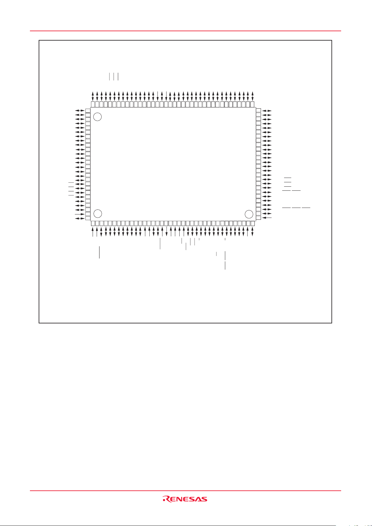
Under development
This document is under development and its contents are subject to change.
M16C/6N Group (M16C/6NL, M16C/6NN) 1. Overview
PIN CONFIGURATION (top view)
P1_0
P0_7/AN0_7
P0_6/AN0_6
P0_5/AN0_5
P0_4/AN0_4
P0_3/AN0_3
P0_2/AN0_2
P0_1/AN0_1
P0_0/AN0_0
P11_7/SIN6
P11_6/SOUT6
P11_5/CLK6
P11_4
P11_3
P11_2/SOUT5
P11_1/SIN5
P11_0/CLK5
P10_7/AN7/KI3
P10_6/AN6/KI2
P10_5/AN5/KI1
P10_4/AN4/KI0
P10_3/AN3
P10_2/AN2
P10_1/AN1
AVSS
P10_0/AN0
103
104
105
106
107
108
109
110
111
112
113
114
115
116
117
118
119
120
121
122
123
124
125
126
127
128
P1_1
P1_2
P1_5/INT3
P1_4
P1_3
P1_6/INT4
100101102
VREF
AVCC
P9_4/DA1/TB4IN
P9_7/ADTRG/SIN4
P9_5/ANEX0/CRX0/CLK4
P9_6/ANEX1/CTX0/SOUT4
P2_3/AN2_3
P2_2/AN2_2
P2_1/AN2_1
P1_7/INT5
P2_0/AN2_0
P2_4/AN2_4
P14_1
P14_0
P9_3/DA0/TB3IN
P9_1/TB1IN/SIN3
P9_0/TB0IN/CLK3
P9_2/TB2IN/SOUT3
(1)
VSS
VCC2
P12_1
P12_0
P12_3
P3_0
P12_2
P2_7/AN2_7
P2_6/AN2_6
P2_5/AN2_5
M16C/6N Group
(M16C/6NN)
21 22 23 24 25 26 27 28 29 3011 12 13 14 15 16 17 18 19 2012345678910
XIN
RESET
P8_7/XCIN
P8_6/XCOUT
VSS
XOUT
VCC1
P8_5/NMI
P8_4/INT2/ZP
BYTE
CNVSS
P12_4
P3_1
P8_2/INT0
P8_3/INT1
P3_3
P3_2
P8_1/TA4IN/U
P4_3
P4_2
P4_1
P4_0
P3_7
P3_6
P3_5
P3_4
737475767778798081828384858687888990919293949596979899
31 32 33 34 35 36 37
P7_7/TA3IN
P7_6/TA3OUT
P8_0/TA4OUT/U/(SIN4)
P7_2/CLK2/TA1OUT/V
P7_5/TA2IN/W/(SOUT4)
P7_4/TA2OUT/W/(CLK4)
P7_3/CTS2/RTS2/TA1IN/V
P7_1/RXD2/SCL2/TA0IN/TB5IN
(1)
P4_7
P4_6
P4_5
P4_4
66676869707172
65
64
P12_5
63
P12_6
62
P12_7
61
P5_0
60
P5_1
59
P5_2
58
P5_3
57
P13_0
56
P13_1
55
P13_2
54
P13_3
53
P5_4
52
P5_5
51
P5_6
50
P5_7/CLKOUT
49
P13_4
48
P13_5/INT6
47
P13_6/INT7
46
P13_7/INT8
45
P6_0/CTS0/RTS0
44
P6_1/CLK0
43
P6_2/RXD0/SCL0
42
P6_3/TXD0/SDA0
41
P6_4/CTS1/RTS1/CTS0/CLKS1
40
P6_5/CLK1
39
38
VSS
VCC1
P6_7/TXD1/SDA1
P6_6/RXD1/SCL1
P7_0/TXD2/SDA2/TA0OUT
1. P7_1 and P9_1 are N channel open-drain pins.
Figure 1.4 Pin Configuration (Top View) (2)
Package: PLQP0128KB-ANOTE:
Rev.1.02 Jul 01, 2005 page 7 of 314
REJ09B0126-0102
Page 24
Under development
This document is under development and its contents are subject to change.
M16C/6N Group (M16C/6NL, M16C/6NN) 1. Overview
1.6 Pin Description
Tables 1.4 and 1.5 list the pin descriptions.
Table 1.4 Pin Description (100-pin and 128-pin Versions) (1)
Signal Name Pin Name I/O Type Description
Power supply
input
Analog power
supply input
Reset input
CNVSS
External data
VCC1, VCC2,
VSS
AVCC, AVSS
_____________
RESET
CNVSS
BYTE
bus width
select input
Main clock
XIN
input
Main clock
XOUT
output
Sub clock
XCIN
input
Sub clock
XCOUT
output
Clock output
______
INT interrupt input
_______
NMI interrupt
input
Key input
CLKOUT
________ ________
INT0 to INT8
________
NMI
______ ______
KI0 to KI3
(3)
interrupt input
Timer A
TA0OUT to TA4OUT
I/O
TA0IN to TA4IN
ZP
Timer B
Three-phase motor
control output
Serial I/O
TB0IN to TB5IN
___ ___ ____
U, U, V, V, W, W
__________ __________
CTS0 to CTS2
__________ __________
RTS0 to RTS2
CLK0 to CLK6
(3)
I/O
RXD0 to RXD2
SIN3 to SIN6
(3)
TXD0 to TXD2
SOUT3 to SOUT6
(3)
CLKS1
2
I
C mode
SDA0 to SDA2
SCL0 to SCL2
I/O
I/O
I: Input O: Output I/O: Input/Output
Apply 3.0 to 5.5V to the VCC1 and VCC2 pins and 0V to the
I
VSS pin. The VCC apply condition is that VCC2 = VCC1
Applies the power supply for the A/D converter. Connect the
I
AVCC pin to VCC1. Connect the AVSS pin to VSS.
The microcomputer is in a reset state when applying “L” to the
I
this pin.
Connect this pin to VSS.
I
Connect this pin to VSS.
I
I/O pins for the main clock oscillation circuit. Connect a ceramic
I
resonator or crystal oscillator between XIN and XOUT
To use the external clock, input the clock from XIN and leave
O
XOUT open.
I/O pins for a sub clock oscillation circuit. Connect a crystal
I
oscillator between XCIN and XCOUT
To use the external clock, input the clock from XCIN and leave
O
(2)
.
XCOUT open.
The clock of the same cycle as fC, f8, or f32 is output.
O
Input pins for the INT interrupt.
I
Input pin for the NMI interrupt.
I
Input pins for the key input interrupt.
I
______
_______
These are timer A0 to timer A4 I/O pins.
These are timer A0 to timer A4 input pins.
I
Input pin for the Z-phase.
I
These are timer B0 to timer B5 input pins.
I
These are Three-phase motor control output pins.
O
These are send control input pins.
I
These are receive control output pins.
O
These are transfer clock I/O pins.
These are serial data input pins.
I
These are serial data input pins.
I
These are serial data output pins.
O
These are serial data output pins.
O
This is output pin for transfer clock output from multiple pins function.
O
These are serial data I/O pins.
These are transfer clock I/O pins. (except SCL2 for the
N-channel open drain output.)
(1)
.
(2)
.
NOTES:
1. In this manual, hereafter, VCC refers to VCC1 unless otherwise noted.
2. Ask the oscillator maker the oscillation characteristic.
________ ________
3. INT6 to INT8, CLK5, CLK6, SIN5, SIN6, SOUT5, SOUT6 are only in the 128-pin version.
Rev.1.02 Jul 01, 2005 page 8 of 314
REJ09B0126-0102
Page 25

Under development
This document is under development and its contents are subject to change.
M16C/6N Group (M16C/6NL, M16C/6NN) 1. Overview
Table 1.5 Pin Description (100-pin and 128-pin Versions) (2)
Signal Name Pin Name I/O Type Description
Reference
voltage input
A/D converter
VREF
AN0 to AN7
Applies the reference voltage for the A/D converter and D/A
I
converter.
Analog input pins for the A/D converter.
I
AN0_0 to AN0_7
AN2_0 to AN2_7
_____________
ADTRG
ANEX0
I/O
This is an A/D trigger input pin.
I
This is the extended analog input pin for the A/D converter,
and is the output in external op-amp connection mode.
D/A converter
CAN module
I/O port
ANEX1
DA0, DA1
CRX0
CTX0
P0_0 to P0_7
P1_0 to P1_7
P2_0 to P2_7
P3_0 to P3_7
P4_0
to
P4_7
P5_0 to P5_7
I/O
This is the extended analog input pin for the A/D converter.
I
These are the output pins for the D/A converter.
O
This is the input pin for the CAN module.
I
This is the output pin for the CAN module.
O
8-bit I/O ports in CMOS, having a direction register to select
an input or output.
Each pin is set as an input port or output port. An input port
can be set for a pull-up or for no pull-up in 4-bit unit by
program.
(except P7_1 and P9_1 for the N-channel open drain output.)
P6_0 to P6_7
P7_0 to P7_7
P8_0 to P8_4
P8_6, P8_7
P9_0 to P9_7
P10_0 to P10_7
(1)
(1)
(1)
(1)
I
Input pin for the NMI interrupt.
_______
Input port
P11_0 to P11_7
P12_0 to P12_7
P13_0 to P13_7
P14_0, P14_1
P8_5
Pin states can be read by the P8_5 bit in the P8 register.
I: Input O: Output I/O: Input/Output
NOTE:
1. Ports P11 to P14 are only in the 128-pin version.
Rev.1.02 Jul 01, 2005 page 9 of 314
REJ09B0126-0102
Page 26
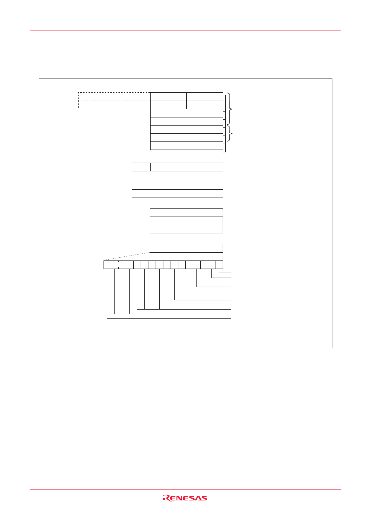
Under development
This document is under development and its contents are subject to change.
M16C/6N Group (M16C/6NL, M16C/6NN) 2. Central Processing Unit (CPU)
2. Central Processing Unit (CPU)
Figure 2.1 shows the CPU registers. The CPU has 13 registers. Of these, R0, R1, R2, R3, A0, A1 and FB
comprise a register bank. There are two register banks.
b31 b15 b8 b7 b0
R2
R3
R0H (R0's high bits) R0L (R0's low bits)
R1H (R1's high bits) R1L (R1's low bits)
R2
R3
A0
A1
FB
Data Registers
Address Registers
Frame Base Registers
(1)
(1)
(1)
b19 b15
INTBLINTBH
The upper 4 bits of INTB are INTBH and the lower 16 bits of INTB are INTBL.
b19
PC
b15 b0
USP
ISP
SB
b15 b0
FLG
b15 b0
IPL U I O B S Z D C
NOTE:
1. These registers comprise a register bank. There are two register banks.
b7b8
b0
Interrupt Table Register
b0
Program Counter
User Stack Pointer
Interrupt Stack Pointer
Static Base Register
Flag Register
Carry Flag
Debug Flag
Zero Flag
Sign Flag
Register Bank Select Flag
Overflow Flag
Interrupt Enable Flag
Stack Pointer Select Flag
Reserved Area
Processor Interrupt Priority Level
Reserved Area
Figure 2.1 CPU Registers
2.1 Data Registers (R0, R1, R2, and R3)
The R0 register consists of 16 bits, and is used mainly for transfers and arithmetic/logic operations. R1 to
R3 are the same as R0.
The R0 register can be separated between high (R0H) and low (R0L) for use as two 8-bit data registers.
R1H and R1L are the same as R0H and R0L. Conversely R2 and R0 can be combined for use as a 32-bit
data register (R2R0). R3R1 is the same as R2R0.
2.2 Address Registers (A0 and A1)
The A0 register consists of 16 bits, and is used for address register indirect addressing and address
register relative addressing. They also are used for transfers and arithmetic/logic operations. A1 is the
same as A0.
In some instructions, A1 and A0 can be combined for use as a 32-bit address register (A1A0).
Rev.1.02 Jul 01, 2005 page 10 of 314
REJ09B0126-0102
Page 27

Under development
This document is under development and its contents are subject to change.
M16C/6N Group (M16C/6NL, M16C/6NN) 2. Central Processing Unit (CPU)
2.3 Frame Base Register (FB)
FB is configured with 16 bits, and is used for FB relative addressing.
2.4 Interrupt Table Register (INTB)
INTB is configured with 20 bits, indicating the start address of an interrupt vector table.
2.5 Program Counter (PC)
PC is configured with 20 bits, indicating the address of an instruction to be executed.
2.6 User Stack Pointer (USP), Interrupt Stack Pointer (ISP)
Stack pointer (SP) comes in two types: USP and ISP, each configured with 16 bits.
Your desired type of stack pointer (USP or ISP) can be selected by the U flag of FLG.
2.7 Static Base Register (SB)
SB is configured with 16 bits, and is used for SB relative addressing.
2.8 Flag Register (FLG)
FLG consists of 11 bits, indicating the CPU status.
2.8.1 Carry Flag (C Flag)
This flag retains a carry, borrow, or shift-out bit that has occurred in the arithmetic/logic unit.
2.8.2 Debug Flag (D Flag)
This flag is used exclusively for debugging purpose. During normal use, it must be set to “0”.
2.8.3 Zero Flag (Z Flag)
This flag is set to “1” when an arithmetic operation resulted in 0; otherwise, it is “0”.
2.8.4 Sign Flag (S Flag)
This flag is set to “1” when an arithmetic operation resulted in a negative value; otherwise, it is “0”.
2.8.5 Register Bank Select Flag (B Flag)
Register bank 0 is selected when this flag is “0” ; register bank 1 is selected when this flag is “1”.
2.8.6 Overflow Flag (O Flag)
This flag is set to “1” when the operation resulted in an overflow; otherwise, it is “0”.
2.8.7 Interrupt Enable Flag (I Flag)
This flag enables a maskable interrupt.
Maskable interrupts are disabled when the I flag is “0”, and are enabled when the I flag is “1”. The I flag is
set to “0” when the interrupt request is accepted.
2.8.8 Stack Pointer Select Flag (U Flag)
ISP is selected when the U flag is “0” ; USP is selected when the U flag is “1”.
The U flag is set to “0” when a hardware interrupt request is accepted or an INT instruction for software
interrupt Nos. 0 to 31 is executed.
2.8.9 Processor Interrupt Priority Level (IPL)
IPL is configured with three bits, for specification of up to eight processor interrupt priority levels from level
0 to level 7.
If a requested interrupt has priority greater than IPL, the interrupt request is enabled.
2.8.10 Reserved Area
When white to this bit, write “0”. When read, its content is indeterminate.
Rev.1.02 Jul 01, 2005 page 11 of 314
REJ09B0126-0102
Page 28
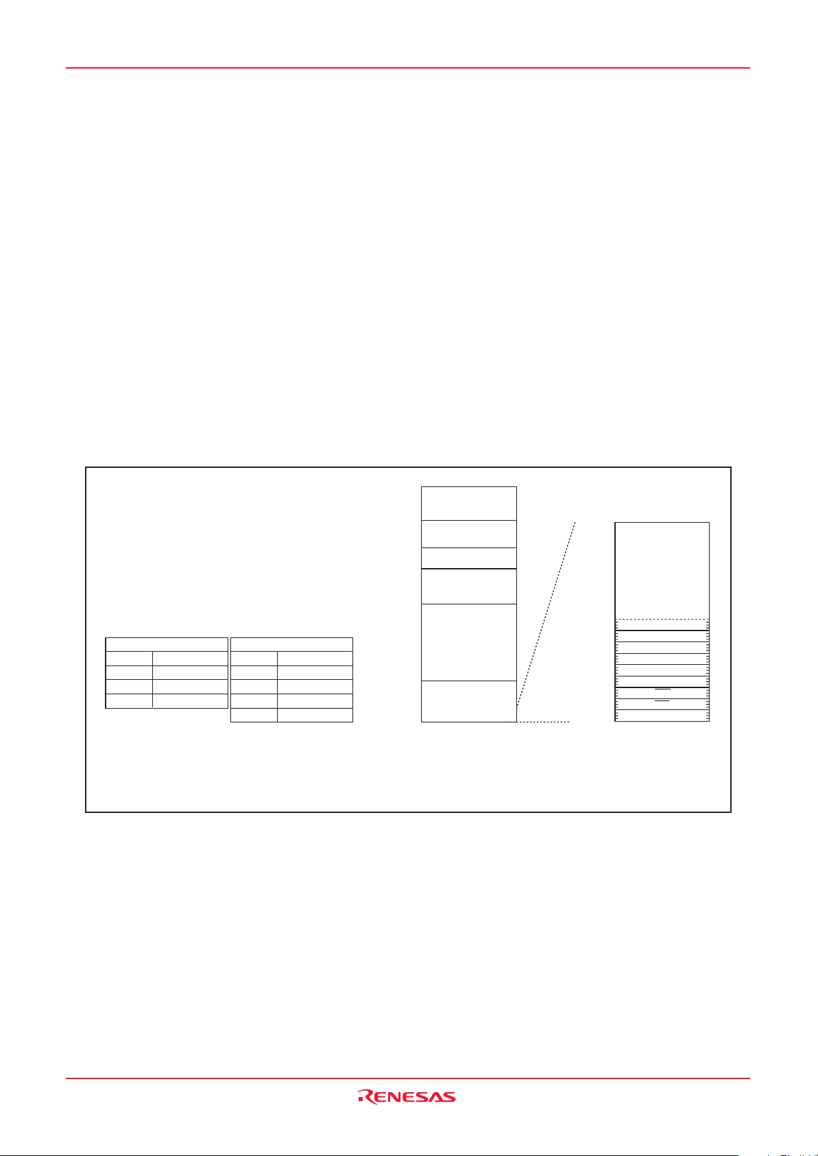
Under development
This document is under development and its contents are subject to change.
M16C/6N Group (M16C/6NL, M16C/6NN) 3. Memory
3. Memory
Figure 3.1 shows a memory map of the M16C/6N Group (M16C/6NL, M16C/6NN). The address space
extends the 1 Mbyte from address 00000h to FFFFFh.
The internal ROM is allocated in a lower address direction beginning with address FFFFFh. For example, a
512-Kbyte internal ROM is allocated to the addresses from 80000h to FFFFFh.
As for the flash memory version, 4-Kbyte space (block A) exists in 0F000h to 0FFFFh. 4-Kbyte space is
mainly for storing data. In addition to storing data, 4-Kbyte space also can store programs.
The fixed interrupt vector table is allocated to the addresses from FFFDCh to FFFFFh. Therefore, store the
start address of each interrupt routine here.
The internal RAM is allocated in an upper address direction beginning with address 00400h. For example, a
31-Kbyte internal RAM is allocated to the addresses from 00400h to 07FFFh. In addition to storing data, the
internal RAM also stores the stack used when calling subroutines and when interrupts are generated.
The SFR is allocated to the addresses from 00000h to 003FFh. Peripheral function control registers are
located here. Of the SFR, any area which has no functions allocated is reserved for future use and cannot be
used by users.
The special page vector table is allocated to the addresses from FFE00h to FFFDBh. This vector is used by
the JMPS or JSRS instruction. For details, refer to M16C/60 and M16C/20 Series Software Manual.
00000h
00400h
h
h
(program area)
Internal RAM
Reserved area
Internal ROM
(data area)
Reserved area
Internal ROM
Internal RAM
Capacity
16 Kbytes 043FF
20 Kbytes
31 Kbytes
Address XXXXX
053FF
07FFF
h
Capacity
h
192 Kbytes D0000
h
256 Kbytes C0000
h
384 Kbytes A0000
512 Kbytes 80000
Internal ROM
Address YYYYY
XXXXX
0F000h
0FFFFh
10000h
(1)
h
h
h
h
h
YYYYY
FFFFFh
NOTES:
1. As for the flash memory version, 4-Kbyte space (block A) exists.
2. Shown here is a memory map for the case where the PM13 bit in the PM1 register is "1".
If the PM13 bit is set to "0", 15 Kbytes of the internal RAM and 192 Kbytes of the internal ROM can be used.
3. When using the masked ROM version, write nothing to internal ROM area.
Figure 3.1 Memory Map
SFR
FFE00h
Special page
(1)
FFFDCh
(3)
FFFFFh
vector table
Undefined instruction
Overflow
BRK instruction
Address match
Single step
Oscillation stop and re-oscillation
detection / watchdog timer
DBC
NMI
Reset
Rev.1.02 Jul 01, 2005 page 12 of 314
REJ09B0126-0102
Page 29
Under development
This document is under development and its contents are subject to change.
M16C/6N Group (M16C/6NL, M16C/6NN) 4. Special Function Register (SFR)
4. Special Function Register (SFR)
SFR (Special Function Register) is the control register of peripheral functions.
Tables 4.1 to 4.12 list the SFR information.
Table 4.1 SFR Information (1)
Address Register Symbol After Reset
0000h
0001h
0002h
0003h
0004h
0005h
0006h
0007h
0008h
0009h
000Ah
000Bh
000Ch
000Dh
000Eh
000Fh
0010h
0011h
0012h
0013h
0014h
0015h
0016h
0017h
0018h
0019h
001Ah
001Bh
001Ch
001Dh
001Eh
001Fh
0020h
0021h
0022h
0023h
0024h
0025h
0026h
0027h
0028h
0029h
002Ah
002Bh
002Ch
002Dh
002Eh
002Fh
0030h
0031h
0032h
0033h
0034h
0035h
0036h
0037h
0038h
0039h
003Ah
003Bh
003Ch
003Dh
003Eh
003Fh
X: Undefined
Processor Mode Register 0
Processor Mode Register 1
System Clock Control Register 0
System Clock Control Register 1
Address Match Interrupt Enable Register
Protect Register
Oscillation Stop Detection Register
Watchdog Timer Start Register
Watchdog Timer Control Register
Address Match Interrupt Register 0
Address Match Interrupt Register 1
PLL Control Register 0
Processor Mode Register 2
DMA0 Source Pointer
DMA0 Destination Pointer
DMA0 Transfer Counter
DMA0 Control Register
DMA1 Source Pointer
DMA1 Destination Pointer
DMA1 Transfer Counter
DMA1 Control Register
(1)
PM0
PM1
CM0
CM1
AIER
PRCR
CM2
WDTS
WDC
RMAD0
RMAD1
PLC0
PM2
SAR0
DAR0
TCR0
DM0CON
SAR1
DAR1
TCR1
DM1CON
00h
00001000b
01001000b
00100000b
XXXXXX00b
XX000000b
0X000000b
XXh
00XXXXXXb
00h
00h
X0h
00h
00h
X0h
0001X010b
XXX00000b
XXh
XXh
XXh
XXh
XXh
XXh
XXh
XXh
00000X00b
XXh
XXh
XXh
XXh
XXh
XXh
XXh
XXh
00000X00b
NOTES:
1. The CM20, CM21, and CM27 bits in the CM2 register do not change at oscillation stop detection reset.
2. The blank areas are reserved and cannot be accessed by users.
Rev.1.02 Jul 01, 2005 page 13 of 314
REJ09B0126-0102
Page 30
Under development
This document is under development and its contents are subject to change.
M16C/6N Group (M16C/6NL, M16C/6NN) 4. Special Function Register (SFR)
Table 4.2 SFR Information (2)
Address Register
0040h
0041h
0042h
0043h
0044h
0045h
0046h
0047h
0048h
0049h
004Ah
004Bh
004Ch
004Dh
004Eh
004Fh
0050h
0051h
0052h
0053h
0054h
0055h
0056h
0057h
0058h
0059h
005Ah
005Bh
005Ch
005Dh
005Eh
005Fh
0060h
CAN0 Wake-up Interrupt Control Register
CAN0 Successful Reception Interrupt Control Register
CAN0 Successful Transmission Interrupt Control Register
INT3 Interrupt Control Register
Timer B5 Interrupt Control Register
SI/O5 Interrupt Control Register
(1)
Timer B4 Interrupt Control Register
UART1 Bus Collision Detection Interrupt Control Register
Timer B3 Interrupt Control Register
UART0 Bus Collision Detection Interrupt Control Register
SI/O4 Interrupt Control Register
INT5 Interrupt Control Register
SI/O3 Interrupt Control Register
INT4 Interrupt Control Register
UART2 Bus Collision Detection Interrupt Control Register
DMA0 Interrupt Control Register
DMA1 Interrupt Control Register
CAN0 Error Interrupt Control Register
A/D Conversion Interrupt Control Register
Key Input Interrupt Control Register
UART2 Transmit Interrupt Control Register
UART2 Receive Interrupt Control Register
UART0 Transmit Interrupt Control Register
UART0 Receive Interrupt Control Register
UART1 Transmit Interrupt Control Register
UART1 Receive Interrupt Control Register
Timer A0 Interrupt Control Register
Timer A1 Interrupt Control Register
Timer A2 Interrupt Control Register
INT7 Interrupt Control Register
Timer A3 Interrupt Control Register
INT6 Interrupt Control Register
(1)
(1)
Timer A4 Interrupt Control Register
Timer B0 Interrupt Control Register
SI/O6 Interrupt Control Register
Timer B1 Interrupt Control Register
INT8 Interrupt Control Register
(1)
(1)
Timer B2 Interrupt Control Register
INT0 Interrupt Control Register
INT1 Interrupt Control Register
INT2 Interrupt Control Register
0061h
0062h
0063h
CAN0 Message Box 0: Identifier / DLC
0064h
0065h
0066h
0067h
0068h
0069h
006Ah
CAN0 Message Box 0: Data Field
006Bh
006Ch
006Dh
006Eh
006Fh
CAN0 Message Box 0: Time Stamp
0070h
0071h
0072h
0073h
CAN0 Message Box 1: Identifier / DLC
0074h
0075h
0076h
0077h
0078h
0079h
007Ah
CAN0 Message Box 1: Data Field
007Bh
007Ch
007Dh
007Eh
007Fh
CAN0 Message Box 1: Time Stamp
X: Undefined
Symbol After Reset
C01WKIC
C0RECIC
C0TRMIC
INT3IC
TB5IC
S5IC
TB4IC
U1BCNIC
TB3IC
U0BCNIC
S4IC
INT5IC
S3IC
INT4IC
U2BCNIC
DM0IC
DM1IC
C01ERRIC
ADIC
KUPIC
S2TIC
S2RIC
S0TIC
S0RIC
S1TIC
S1RIC
TA0IC
TA1IC
TA2IC
INT7IC
TA3IC
INT6IC
TA4IC
TB0IC
S6IC
TB1IC
INT8IC
TB2IC
INT0IC
INT1IC
INT2IC
XXXXX000b
XXXXX000b
XXXXX000b
XX00X000b
XXXXX000b
XXXXX000b
XXXXX000b
XX00X000b
XX00X000b
XXXXX000b
XXXXX000b
XXXXX000b
XXXXX000b
XXXXX000b
XXXXX000b
XXXXX000b
XXXXX000b
XXXXX000b
XXXXX000b
XXXXX000b
XXXXX000b
XXXXX000b
XX00X000b
XX00X000b
XXXXX000b
XXXXX000b
XX00X000b
XXXXX000b
XX00X000b
XX00X000b
XX00X000b
XXh
XXh
XXh
XXh
XXh
XXh
XXh
XXh
XXh
XXh
XXh
XXh
XXh
XXh
XXh
XXh
XXh
XXh
XXh
XXh
XXh
XXh
XXh
XXh
XXh
XXh
XXh
XXh
XXh
XXh
XXh
XXh
NOTES:
1. These registers exist only in the 128-pin version.
2. The blank area is reserved and cannot be accessed by users.
Rev.1.02 Jul 01, 2005 page 14 of 314
REJ09B0126-0102
Page 31

Under development
This document is under development and its contents are subject to change.
M16C/6N Group (M16C/6NL, M16C/6NN) 4. Special Function Register (SFR)
Table 4.3 SFR Information (3)
Address Register Symbol After Reset
0080h
0081h
0082h
0083h
0084h
0085h
0086h
0087h
0088h
0089h
008Ah
008Bh
008Ch
008Dh
008Eh
008Fh
0090h
0091h
0092h
0093h
0094h
0095h
0096h
0097h
0098h
0099h
009Ah
009Bh
009Ch
009Dh
009Eh
009Fh
00A0h
00A1h
00A2h
00A3h
00A4h
00A5h
00A6h
00A7h
00A8h
00A9h
00AAh
00ABh
00ACh
00ADh
00AEh
00AFh
00B0h
00B1h
00B2h
00B3h
00B4h
00B5h
00B6h
00B7h
00B8h
00B9h
00BAh
00BBh
00BCh
00BDh
00BEh
00BFh
X: Undefined
CAN0 Message Box 2: Identifier / DLC
CAN0 Message Box 2: Data Field
CAN0 Message Box 2: Time Stamp
CAN0 Message Box 3: Identifier / DLC
CAN0 Message Box 3: Data Field
CAN0 Message Box 3: Time Stamp
CAN0 Message Box 4: Identifier / DLC
CAN0 Message Box 4: Data Field
CAN0 Message Box 4: Time Stamp
CAN0 Message Box 5: Identifier / DLC
CAN0 Message Box 5: Data Field
CAN0 Message Box 5: Time Stamp
XXh
XXh
XXh
XXh
XXh
XXh
XXh
XXh
XXh
XXh
XXh
XXh
XXh
XXh
XXh
XXh
XXh
XXh
XXh
XXh
XXh
XXh
XXh
XXh
XXh
XXh
XXh
XXh
XXh
XXh
XXh
XXh
XXh
XXh
XXh
XXh
XXh
XXh
XXh
XXh
XXh
XXh
XXh
XXh
XXh
XXh
XXh
XXh
XXh
XXh
XXh
XXh
XXh
XXh
XXh
XXh
XXh
XXh
XXh
XXh
XXh
XXh
XXh
XXh
Rev.1.02 Jul 01, 2005 page 15 of 314
REJ09B0126-0102
Page 32

Under development
This document is under development and its contents are subject to change.
M16C/6N Group (M16C/6NL, M16C/6NN) 4. Special Function Register (SFR)
Table 4.4 SFR Information (4)
Address Register Symbol After Reset
00C0h
00C1h
00C2h
00C3h
00C4h
00C5h
00C6h
00C7h
00C8h
00C9h
00CAh
00CBh
00CCh
00CDh
00CEh
00CFh
00D0h
00D1h
00D2h
00D3h
00D4h
00D5h
00D6h
00D7h
00D8h
00D9h
00DAh
00DBh
00DCh
00DDh
00DEh
00DFh
00E0h
00E1h
00E2h
00E3h
00E4h
00E5h
00E6h
00E7h
00E8h
00E9h
00EAh
00EBh
00ECh
00EDh
00EEh
00EFh
00F0h
00F1h
00F2h
00F3h
00F4h
00F5h
00F6h
00F7h
00F8h
00F9h
00FAh
00FBh
00FCh
00FDh
00FEh
00FFh
X: Undefined
CAN0 Message Box 6: Identifier / DLC
CAN0 Message Box 6: Data Field
CAN0 Message Box 6: Time Stamp
CAN0 Message Box 7: Identifier / DLC
CAN0 Message Box 7: Data Field
CAN0 Message Box 7: Time Stamp
CAN0 Message Box 8: Identifier / DLC
CAN0 Message Box 8: Data Field
CAN0 Message Box 8: Time Stamp
CAN0 Message Box 9: Identifier / DLC
CAN0 Message Box 9: Data Field
CAN0 Message Box 9: Time Stamp
XXh
XXh
XXh
XXh
XXh
XXh
XXh
XXh
XXh
XXh
XXh
XXh
XXh
XXh
XXh
XXh
XXh
XXh
XXh
XXh
XXh
XXh
XXh
XXh
XXh
XXh
XXh
XXh
XXh
XXh
XXh
XXh
XXh
XXh
XXh
XXh
XXh
XXh
XXh
XXh
XXh
XXh
XXh
XXh
XXh
XXh
XXh
XXh
XXh
XXh
XXh
XXh
XXh
XXh
XXh
XXh
XXh
XXh
XXh
XXh
XXh
XXh
XXh
XXh
Rev.1.02 Jul 01, 2005 page 16 of 314
REJ09B0126-0102
Page 33

Under development
This document is under development and its contents are subject to change.
M16C/6N Group (M16C/6NL, M16C/6NN) 4. Special Function Register (SFR)
Table 4.5 SFR Information (5)
Address Register Symbol After Reset
0100h
0101h
0102h
0103h
0104h
0105h
0106h
0107h
0108h
0109h
010Ah
010Bh
010Ch
010Dh
010Eh
010Fh
0110h
0111 h
0112h
0113h
0114h
0115h
0116h
0117h
0118h
0119h
011Ah
011Bh
011Ch
011Dh
011Eh
011Fh
0120h
0121h
0122h
0123h
0124h
0125h
0126h
0127h
0128h
0129h
012Ah
012Bh
012Ch
012Dh
012Eh
012Fh
0130h
0131h
0132h
0133h
0134h
0135h
0136h
0137h
0138h
0139h
013Ah
013Bh
013Ch
013Dh
013Eh
013Fh
X: Undefined
CAN0 Message Box 10: Identifier / DLC
CAN0 Message Box 10: Data Field
CAN0 Message Box 10: Time Stamp
CAN0 Message Box 11: Identifier / DLC
CAN0 Message Box 11: Data Field
CAN0 Message Box 11: Time Stamp
CAN0 Message Box 12: Identifier / DLC
CAN0 Message Box 12: Data Field
CAN0 Message Box 12: Time Stamp
CAN0 Message Box 13: Identifier / DLC
CAN0 Message Box 13: Data Field
CAN0 Message Box 13: Time Stamp
XXh
XXh
XXh
XXh
XXh
XXh
XXh
XXh
XXh
XXh
XXh
XXh
XXh
XXh
XXh
XXh
XXh
XXh
XXh
XXh
XXh
XXh
XXh
XXh
XXh
XXh
XXh
XXh
XXh
XXh
XXh
XXh
XXh
XXh
XXh
XXh
XXh
XXh
XXh
XXh
XXh
XXh
XXh
XXh
XXh
XXh
XXh
XXh
XXh
XXh
XXh
XXh
XXh
XXh
XXh
XXh
XXh
XXh
XXh
XXh
XXh
XXh
XXh
XXh
Rev.1.02 Jul 01, 2005 page 17 of 314
REJ09B0126-0102
Page 34

Under development
This document is under development and its contents are subject to change.
M16C/6N Group (M16C/6NL, M16C/6NN) 4. Special Function Register (SFR)
Table 4.6 SFR Information (6)
Address Register Symbol After Reset
0140h
0141h
0142h
0143h
0144h
0145h
0146h
0147h
0148h
0149h
014Ah
014Bh
014Ch
014Dh
014Eh
014Fh
0150h
0151h
0152h
0153h
0154h
0155h
0156h
0157h
0158h
0159h
015Ah
015Bh
015Ch
015Dh
015Eh
015Fh
0160h
0161h
0162h
0163h
0164h
0165h
0166h
0167h
0168h
0169h
016Ah
016Bh
016Ch
016Dh
016Eh
016Fh
0170h
0171h
0172h
0173h
0174h
0175h
0176h
0177h
0178h
0179h
017Ah
017Bh
017Ch
017Dh
017Eh
017Fh
X: Undefined
CAN0 Message Box 14: Identifier /DLC
CAN0 Message Box 14: Data Field
CAN0 Message Box 14: Time Stamp
CAN0 Message Box 15: Identifier /DLC
CAN0 Message Box 15: Data Field
CAN0 Message Box 15: Time Stamp
CAN0 Global Mask Register
CAN0 Local Mask A Register
CAN0 Local Mask B Register
C0GMR
C0LMAR
C0LMBR
XXh
XXh
XXh
XXh
XXh
XXh
XXh
XXh
XXh
XXh
XXh
XXh
XXh
XXh
XXh
XXh
XXh
XXh
XXh
XXh
XXh
XXh
XXh
XXh
XXh
XXh
XXh
XXh
XXh
XXh
XXh
XXh
XXh
XXh
XXh
XXh
XXh
XXh
XXh
XXh
XXh
XXh
XXh
XXh
XXh
XXh
XXh
XXh
XXh
XXh
NOTE:
1. The blank areas are reserved and cannot be accessed by users.
Rev.1.02 Jul 01, 2005 page 18 of 314
REJ09B0126-0102
Page 35

Under development
This document is under development and its contents are subject to change.
M16C/6N Group (M16C/6NL, M16C/6NN) 4. Special Function Register (SFR)
Table 4.7 SFR Information (7)
Address Register Symbol After Reset
0180h
0181h
0182h
0183h
0184h
0185h
0186h
0187h
0188h
0189h
018Ah
018Bh
018Ch
018Dh
018Eh
018Fh
0190h
0191h
0192h
0193h
0194h
0195h
0196h
0197h
0198h
0199h
019Ah
019Bh
019Ch
019Dh
019Eh
019Fh
01A0h
01A1h
01A2h
01A3h
01A4h
01A5h
01A6h
01A7h
01A8h
01A9h
01AAh
01ABh
01ACh
01ADh
01AEh
01AFh
01B0h
01B1h
01B2h
01B3h
01B4h
01B5h
01B6h
01B7h
01B8h
01B9h
01BAh
01BBh
01BCh
01BDh
01BEh
01BFh
X: Undefined
Flash Memory Control Register 1
Flash Memory Control Register 0
Address Match Interrupt Register 2
Address Match Interrupt Enable Register 2
Address Match Interrupt Register 3
(1)
(1)
FMR1
FMR0
RMAD2
AIER2
RMAD3
0X00XX0Xb
00000001b
00h
00h
X0h
XXXXXX00b
00h
00h
X0h
NOTES:
1. These registers are included in the flash memory version. Cannot be accessed by users in the mask ROM version.
2. The blank areas are reserved and cannot be accessed by users.
Rev.1.02 Jul 01, 2005 page 19 of 314
REJ09B0126-0102
Page 36

Under development
This document is under development and its contents are subject to change.
M16C/6N Group (M16C/6NL, M16C/6NN) 4. Special Function Register (SFR)
Table 4.8 SFR Information (8)
Address Register Symbol After Reset
01C0h
Timer B3, B4, B5 Count Start Flag
TBSR
01C1h
01C2h
01C3h
01C4h
01C5h
01C6h
01C7h
01C8h
01C9h
01CAh
01CBh
01CCh
01CDh
Timer A1-1 Register
Timer A2-1 Register
Timer A4-1 Register
Three-Phase PWM Control Register 0
Three-Phase PWM Control Register 1
Three-Phase Output Buffer Register 0
Three-Phase Output Buffer Register 1
Dead Time Timer
Timer B2 Interrupt Occurrence Frequency Set Counter
TA11
TA21
TA41
INVC0
INVC1
IDB0
IDB1
DTT
ICTB2
01CEh
01CFh
01D0h
01D1h
01D2h
01D3h
01D4h
01D5h
01D6h
01D7h
01D8h
01D9h
01DAh
01DBh
01DCh
01DDh
01DEh
01DFh
01E0h
Interrupt Cause Select Register 2
Timer B3 Register
Timer B4 Register
Timer B5 Register
SI/O6 Transmit/Receive Register
SI/O6 Control Register
(1)
SI/O6 Bit Rate Generator
(1)
(1)
SI/O3, 4, 5, 6 Transmit/Receive Register
Timer B3 Mode Register
Timer B4 Mode Register
Timer B5 Mode Register
Interrupt Cause Select Register 0
Interrupt Cause Select Register 1
SI/O3 Transmit/Receive Register
(2)
IFSR2
TB3
TB4
TB5
S6TRR
S6C
S6BRG
S3456TRR
TB3MR
TB4MR
TB5MR
IFSR0
IFSR1
S3TRR
01E1h
01E2h
01E3h
01E4h
SI/O3 Control Register
SI/O3 Bit Rate Generator
SI/O4 Transmit/Receive Register
S3C
S3BRG
S4TRR
01E5h
01E6h
01E7h
01E8h
01E9h
01EAh
01EBh
01ECh
01EDh
01EEh
01EFh
01F0h
01F1h
01F2h
01F3h
01F4h
01F5h
01F6h
01F7h
01F8h
01F9h
01FAh
01FBh
01FCh
01FDh
01FEh
01FFh
SI/O4 Control Register
SI/O4 Bit Rate Generator
SI/O5 Transmit/Receive Register
SI/O5 Control Register
(1)
SI/O5 Bit Rate Generator
(1)
(1)
UART0 Special Mode Register 4
UART0 Special Mode Register 3
UART0 Special Mode Register 2
UART0 Special Mode Register
UART1 Special Mode Register 4
UART1 Special Mode Register 3
UART1 Special Mode Register 2
UART1 Special Mode Register
UART2 Special Mode Register 4
UART2 Special Mode Register 3
UART2 Special Mode Register 2
UART2 Special Mode Register
UART2 Transmit/Receive Mode Register
UART2 Bit Rate Generator
UART2 Transmit Buffer Register
UART2 Transmit/Receive Control Register 0
UART2 Transmit/Receive Control Register 1
UART2 Receive Buffer Register
S4C
S4BRG
S5TRR
S5C
S5BRG
U0SMR4
U0SMR3
U0SMR2
U0SMR
U1SMR4
U1SMR3
U1SMR2
U1SMR
U2SMR4
U2SMR3
U2SMR2
U2SMR
U2MR
U2BRG
U2TB
U2C0
U2C1
U2RB
X: Undefined
000XXXXXb
XXh
XXh
XXh
XXh
XXh
XXh
00h
00h
00h
00h
XXh
XXh
X0000000b
XXh
XXh
XXh
XXh
XXh
XXh
XXh
01000000b
XXh
XXXX0000b
00XX0000b
00XX0000b
00XX0000b
00h
00h
XXh
01000000b
XXh
XXh
01000000b
XXh
XXh
01000000b
XXh
00h
000X0X0Xb
X0000000b
X0000000b
00h
000X0X0Xb
X0000000b
X0000000b
00h
000X0X0Xb
X0000000b
X0000000b
00h
XXh
XXh
XXh
00001000b
00000010b
XXh
XXh
NOTES:
1. These registers exist only in the 128-pin version.
2. The S5TRF and S6TRF bits in the S3456TRR register are used in the 128-pin version.
3. The blank areas are reserved and cannot be accessed by users.
Rev.1.02 Jul 01, 2005 page 20 of 314
REJ09B0126-0102
Page 37

Under development
This document is under development and its contents are subject to change.
M16C/6N Group (M16C/6NL, M16C/6NN) 4. Special Function Register (SFR)
Table 4.9 SFR Information (9)
Address Register Symbol After Reset
0200h
0201h
0202h
0203h
0204h
0205h
0206h
0207h
0208h
0209h
020Ah
020Bh
020Ch
020Dh
020Eh
020Fh
0210h
0211h
0212h
0213h
0214h
0215h
0216h
0217h
0218h
0219h
021Ah
021Bh
021Ch
021Dh
021Eh
021Fh
0220h
0221h
0222h
0223h
0224h
0225h
0226h
0227h
0228h
0229h
022Ah
022Bh
022Ch
022Dh
022Eh
022Fh
0230h
0231h
0232h
0233h
0234h
0235h
0236h
0237h
0238h
0239h
023Ah
023Bh
023Ch
023Dh
023Eh
023Fh
X: Undefined
CAN0 Message Control Register 0
CAN0 Message Control Register 1
CAN0 Message Control Register 2
CAN0 Message Control Register 3
CAN0 Message Control Register 4
CAN0 Message Control Register 5
CAN0 Message Control Register 6
CAN0 Message Control Register 7
CAN0 Message Control Register 8
CAN0 Message Control Register 9
CAN0 Message Control Register 10
CAN0 Message Control Register 11
CAN0 Message Control Register 12
CAN0 Message Control Register 13
CAN0 Message Control Register 14
CAN0 Message Control Register 15
CAN0 Control Register
CAN0 Status Register
CAN0 Slot Status Register
CAN0 Interrupt Control Register
CAN0 Extended ID Register
CAN0 Configuration Register
CAN0 Receive Error Count Register
CAN0 Transmit Error Count Register
CAN0 Time Stamp Register
CAN1 Control Register
C0MCTL0
C0MCTL1
C0MCTL2
C0MCTL3
C0MCTL4
C0MCTL5
C0MCTL6
C0MCTL7
C0MCTL8
C0MCTL9
C0MCTL10
C0MCTL11
C0MCTL12
C0MCTL13
C0MCTL14
C0MCTL15
C0CTLR
C0STR
C0SSTR
C0ICR
C0IDR
C0CONR
C0RECR
C0TECR
C0TSR
C1CTLR
00h
00h
00h
00h
00h
00h
00h
00h
00h
00h
00h
00h
00h
00h
00h
00h
X0000001b
XX0X0000b
00h
X0000001b
00h
00h
00h
00h
00h
00h
XXh
XXh
00h
00h
00h
00h
X0000001b
XX0X0000b
NOTE:
1. The blank areas are reserved and cannot be accessed by users.
Rev.1.02 Jul 01, 2005 page 21 of 314
REJ09B0126-0102
Page 38

Under development
This document is under development and its contents are subject to change.
M16C/6N Group (M16C/6NL, M16C/6NN) 4. Special Function Register (SFR)
Table 4.10 SFR Information (10)
Address Register Symbol After Reset
0240h
0241h
0242h
0243h
0244h
0245h
0246h
0247h
0248h
0249h
024Ah
024Bh
024Ch
024Dh
024Eh
024Fh
0250h
0251h
0252h
0253h
0254h
0255h
0256h
0257h
0258h
0259h
025Ah
025Bh
025Ch
025Dh
025Eh
025Fh
0260h
0261h
0262h
0263h
0264h
0265h
0266h
0267h
0268h
0269h
026Ah
026Bh
026Ch
026Dh
026Eh
026Fh
0270h
to
0372h
0373h
0374h
0375h
0376h
0377h
0378h
0379h
037Ah
037Bh
037Ch
037Dh
037Eh
037Fh
X: Undefined
CAN0 Acceptance Filter Support Register
Peripheral Clock Select Register
CAN0 Clock Select Register
C0AFS
PCLKR
CCLKR
XXh
XXh
00h
00h
NOTE:
1. The blank areas are reserved and cannot be accessed by users.
Rev.1.02 Jul 01, 2005 page 22 of 314
REJ09B0126-0102
Page 39

Under development
This document is under development and its contents are subject to change.
M16C/6N Group (M16C/6NL, M16C/6NN) 4. Special Function Register (SFR)
Table 4.11 SFR Information (11)
Address Register Symbol After Reset
0380h
0381h
0382h
0383h
0384h
0385h
0386h
0387h
0388h
0389h
038Ah
038Bh
038Ch
038Dh
038Eh
038Fh
0390h
0391h
0392h
0393h
0394h
0395h
0396h
0397h
0398h
0399h
039Ah
039Bh
039Ch
039Dh
039Eh
039Fh
03A0h
03A1h
03A2h
03A3h
03A4h
03A5h
03A6h
03A7h
03A8h
03A9h
03AAh
03ABh
03ACh
03ADh
03AEh
03AFh
03B0h
03B1h
03B2h
03B3h
03B4h
03B5h
03B6h
03B7h
03B8h
03B9h
03BAh
03BBh
03BCh
03BDh
03BEh
03BFh
X: Undefined
Count Start Flag
Clock Prescaler Reset Flag
One-Shot Start Flag
Trigger Select Register
Up/Down Flag
Timer A0 Register
Timer A1 Register
Timer A2 Register
Timer A3 Register
Timer A4 Register
Timer B0 Register
Timer B1 Register
Timer B2 Register
Timer A0 Mode Register
Timer A1 Mode Register
Timer A2 Mode Register
Timer A3 Mode Register
Timer A4 Mode Register
Timer B0 Mode Register
Timer B1 Mode Register
Timer B2 Mode Register
Timer B2 Special Mode Register
UART0 Transmit/Receive Mode Register
UART0 Bit Rate Generator
UART0 Transmit Buffer Register
UART0 Transmit/Receive Control Register 0
UART0 Transmit/Receive Control Register 1
UART0 Receive Buffer Register
UART1 Transmit/Receive Mode Register
UART1 Bit Rate Generator
UART1 Transmit Buffer Register
UART1 Transmit/Receive Control Register 0
UART1 Transmit/Receive Control Register 1
UART1 Receive Buffer Register
UART Transmit/Receive Control Register 2
DMA0 Request Cause Select Register
DMA1 Request Cause Select Register
CRC Data Register
CRC Input Register
TABSR
CPSRF
ONSF
TRGSR
UDF
TA0
TA1
TA2
TA3
TA4
TB0
TB1
TB2
TA0MR
TA1MR
TA2MR
TA3MR
TA4MR
TB0MR
TB1MR
TB2MR
TB2SC
U0MR
U0BRG
U0TB
U0C0
U0C1
U0RB
U1MR
U1BRG
U1TB
U1C0
U1C1
U1RB
UCON
DM0SL
DM1SL
CRCD
CRCIN
00h
0XXXXXXXb
00h
00h
(1)
00h
XXh
XXh
XXh
XXh
XXh
XXh
XXh
XXh
XXh
XXh
XXh
XXh
XXh
XXh
XXh
XXh
00h
00h
00h
00h
00h
00XX0000b
00XX0000b
00XX0000b
XXXXXX00b
00h
XXh
XXh
XXh
00001000b
00XX0010b
XXh
XXh
00h
XXh
XXh
XXh
00001000b
00XX0010b
XXh
XXh
X0000000b
00h
00h
XXh
XXh
XXh
NOTES:
1. The TA2P to TA4P bits in the UDF register are set to "0" after reset. However, the contents in these bits are indeterminate when read.
2. The blank areas are reserved and cannot be accessed by users.
Rev.1.02 Jul 01, 2005 page 23 of 314
REJ09B0126-0102
Page 40

Under development
This document is under development and its contents are subject to change.
M16C/6N Group (M16C/6NL, M16C/6NN) 4. Special Function Register (SFR)
Table 4.12 SFR Information (12)
Address Register Symbol After Reset
03C0h
03C1h
03C2h
03C3h
03C4h
03C5h
03C6h
03C7h
03C8h
03C9h
03CAh
03CBh
03CCh
03CDh
03CEh
03CFh
A/D Register 0
A/D Register 1
A/D Register 2
A/D Register 3
A/D Register 4
A/D Register 5
A/D Register 6
A/D Register 7
AD0
AD1
AD2
AD3
AD4
AD5
AD6
AD7
03D0h
03D1h
03D2h
03D3h
03D4h
A/D Control Register 2
ADCON2
03D5h
03D6h
03D7h
03D8h
A/D Control Register 0
A/D Control Register 1
D/A Register 0
ADCON0
ADCON1
DA0
03D9h
03DAh
D/A Register 1
DA1
03DBh
03DCh
03DDh
03DEh
03DFh
03E0h
03E1h
03E2h
03E3h
03E4h
03E5h
03E6h
03E7h
03E8h
03E9h
03EAh
03EBh
03ECh
03EDh
03EEh
03EFh
03F0h
03F1h
03F2h
03F3h
03F4h
03F5h
03F6h
03F7h
03F8h
03F9h
03FAh
03FBh
03FCh
03FDh
03FEh
03FFh
D/A Control Register
Port P14 Control Register
Pull-Up Control Register 3
Port P0 Register
Port P1 Register
Port P0 Direction Register
Port P1 Direction Register
Port P2 Register
Port P3 Register
Port P2 Direction Register
Port P3 Direction Register
Port P4 Register
Port P5 Register
Port P4 Direction Register
Port P5 Direction Register
Port P6 Register
Port P7 Register
Port P6 Direction Register
Port P7 Direction Register
Port P8 Register
Port P9 Register
Port P8 Direction Register
Port P9 Direction Register
Port P10 Register
Port P11 Register
(1)
Port P10 Direction Register
Port P11 Direction Register
Port P12 Register
Port P13 Register
(1)
(1)
Port P12 Direction Register
Port P13 Direction Register
Pull-up Control Register 0
Pull-up Control Register 1
Pull-up Control Register 2
Port Control Register
(1)
(1)
(1)
(1)
(1)
DACON
PC14
PUR3
P0
P1
PD0
PD1
P2
P3
PD2
PD3
P4
P5
PD4
PD5
P6
P7
PD6
PD7
P8
P9
PD8
PD9
P10
P11
PD10
PD11
P12
P13
PD12
PD13
PUR0
PUR1
PUR2
PCR
X: Undefined
XXh
XXh
XXh
XXh
XXh
XXh
XXh
XXh
XXh
XXh
XXh
XXh
XXh
XXh
XXh
XXh
00h
00000XXXb
00h
00h
00h
00h
XX00XXXXb
00h
XXh
XXh
00h
00h
XXh
XXh
00h
00h
XXh
XXh
00h
00h
XXh
XXh
00h
00h
XXh
XXh
00X00000b
00h
XXh
XXh
00h
00h
XXh
XXh
00h
00h
00h
00h
00h
00h
NOTES:
1. These registers exist only in the128-pin version.
2. The blank areas are reserved and cannot be accessed by users.
Rev.1.02 Jul 01, 2005 page 24 of 314
REJ09B0126-0102
Page 41

Under development
This document is under development and its contents are subject to change.
M16C/6N Group (M16C/6NL, M16C/6NN) 5. Reset
5. Reset
Hardware reset, software reset, watchdog timer reset and oscillation stop detection reset are available to
reset the microcomputer.
5.1 Hardware Reset
____________
The microcomputer resets pins, the CPU and SFR by setting the RESET pin. If the supply voltage meets
the recommended operating conditions, the microcomputer resets all pins when an “L” signal is applied to
___________ ____________
the RESET pin (see Table 5.1 Pin Status When RESET Pin Level is “L”). The oscillation circuit is also
reset and the main clock starts oscillation. The microcomputer resets the CPU and SFR when the signal
____________
applied to the RESET pin changes low (“L”) to high (“H”). The microcomputer executes the program in an
address indicated by the reset vector. The internal RAM is not reset. When an “L” signal is applied to the
____________
RESET pin while writing data to the internal RAM, the internal RAM is in an indeterminate state.
Figure 5.1 shows an example of the reset circuit. Figure 5.2 shows a reset sequence. Table 5.1 lists pin
____________
states while the RESET pin is held low (“L”). Figure 5.3 shows CPU register states after reset. Refer to 4.
SFR for SFR states after reset.
5.1.1 Reset on a Stable Supply Voltage
____________
(1) Apply “L” to the RESET pin
(2) Apply 20 or more clock cycles to the XIN pin
____________
(3) Apply “H” to the RESET pin
5.1.2 Power-on Reset
____________
(1) Apply “L” to the RESET pin
(2) Raise the supply voltage to the recommended operating level
(3) Insert td(P-R) ms as wait time for the internal voltage to stabilize
(4) Apply 20 or more clock cycles to the XIN pin
____________
(5) Apply “H” to the RESET pin
5.2 Software Reset
The microcomputer resets pins, the CPU and SFR when the PM03 bit in the PM0 register is set to “1”
(microcomputer reset). Then the microcomputer executes the program in an address determined by the reset vector.
Set the PM03 bit to “1” while the main clock is selected as the CPU clock and the main clock oscillation is stable.
In the software reset, the microcomputer does not reset a part of the SFR. Refer to 4. SFR for details.
5.3 Watchdog Timer Reset
The microcomputer resets pins, the CPU and SFR when the PM12 bit in the PM1 register is set to “1” (reset
when watchdog timer underflows) and the watchdog timer underflows. Then the microcomputer executes
the program in an address determined by the reset vector.
In the watchdog timer reset, the microcomputer does not reset a part of the SFR. Refer to 4. SFR for details.
5.4 Oscillation Stop Detection Reset
The microcomputer resets and stops pins, the CPU and SFR when the CM27 bit in the CM2 register is “0”
(reset at oscillation stop, re-oscillation detection), if it detects main clock oscillation circuit stop. Refer to 7.5
Oscillation Stop and Re-Oscillation Detection Function for details.
In the oscillation stop detection reset, the microcomputer does not reset a part of the SFR. Refer to 4. SFR
for details.
Rev.1.02 Jul 01, 2005 page 25 of 314
REJ09B0126-0102
Page 42

Under development
This document is under development and its contents are subject to change.
M16C/6N Group (M16C/6NL, M16C/6NN) 5. Reset
v o l t a g
Re c o m m e n d e d
operation
e
0 V
RESET
VCC
VCC
NOTE
1. Use the shortest possible wiring to connect external circuit.
Figure 5.1 Example Reset Circuit
VCC
XIN
td(P-R) More than
RESET
BCLK
Address
20 cycle
are needed
R E S E T
0 V
BCLK 28cycles
0.2VCC or
below
FFFFCh
0.2VCC or below
Content of reset vector
FFFFEh
Supply a clock with td(P-R) +20
or more cycles to the XIN pin
Figure 5.2 Reset Sequence
Rev.1.02 Jul 01, 2005 page 26 of 314
REJ09B0126-0102
Page 43

Under development
This document is under development and its contents are subject to change.
M16C/6N Group (M16C/6NL, M16C/6NN) 5. Reset
Table 5.1 Pin Status When RESET Pin Level is “L”
____________
Pin Name Status (CNVSS = VSS)
P0, P1, P2, P3, P4, P5, P6, P7, Input port
P8_0 to P8_4, P8_6, P8_7, P9, P10,
P11, P12, P13, P14_0, P14_1
(2)
NOTE:
1. P11, P12, P13, P14_0 and P14_1 pins are only in the 128-pin version.
b15 b0
0000h
0000h
0000h
0000h
0000h
0000h
0000h
b19
00000h
Content of addresses FFFFEh to FFFFCh
b0
Data Register (R0)
Data Register (R1)
Data Register (R2)
Data Register (R3)
Address Register (A0)
Address Register (A1)
Frame Base Register (FB)
Interrupt Table Register (INTB)
Program Counter (PC)
b15 b0
0000h
0000h
0000h
b15 b0
0000h
b15 b0
b7b8
IPL U I O B S Z D C
Figure 5.3 CPU Register Status After Reset
User Stack Pointer (USP)
Interrupt Stack Pointer (ISP)
Static Base Register (SB)
Flag Register (FLG)
Rev.1.02 Jul 01, 2005 page 27 of 314
REJ09B0126-0102
Page 44

Under development
This document is under development and its contents are subject to change.
M16C/6N Group (M16C/6NL, M16C/6NN) 6. Processor Mode
6. Processor Mode
Three processor mode is available single-chip mode only.
Figures 6.1 and 6.2 show the processor mode related registers. Figure 6.3 shows the memory map.
Processor Mode Register 0
b7 b6 b5 b4 b3 b2 b1 b0
0000 000
NOTE:
1. Write to this register after setting the PRC1 bit in the PRCR register to "1" (write enable).
(1)
Symbol Address After Reset
00hPM0 0004h
Bit Symbol
PM00
PM01
-
(b2)
PM03
-
(b7-b4)
Processor Mode Bit
Reserved Bit
Software Reset Bit
Reserved Bit
Bit Name Function
b1 b0
0 0 : Single-chip mode
0 1 :
1 0 : Do not set a value
1 1 :
Set to "0"
Setting this bit to "1" resets the
microcomputer. When read, its
.
content is "0".
Figure 6.1 PM0 Register
RW
RW
RW
RW
RW
RWSet to "0"
Rev.1.02 Jul 01, 2005 page 28 of 314
REJ09B0126-0102
Page 45

Under development
This document is under development and its contents are subject to change.
M16C/6N Group (M16C/6NL, M16C/6NN) 6. Processor Mode
Processor Mode Register 1
b7 b6 b5 b4 b3 b2 b1 b0
000 0
(1)
Symbol Address After Reset
PM1 0005h 00001000b
Bit Symbol
PM10
-
(b1)
PM12
PM13
-
(b6-b4)
PM17
Data Block Enable Bit
Reserved Bit
Watchdog Timer Function
Select Bit
Internal Reserved Area
Expansion Bit
Reserved Bit
Wait Bit
Bit Name Function
0 :
(2)
(4)
(5)
Block A disable
1 :
Block A enable
Set to "0"
0 : Watchdog timer interrupt
1 : Watchdog timer reset
See NOTE 6
Set to "0"
0 : No wait state
1 : With wait state (1 wait)
(3)
NOTES:
1. Write to this register after setting the PRC1 bit in the PRCR register to "1" (write enable).
2. Set the PM10 bit to "0" for Mask ROM version.
For the flash memory version, when the PM10 bit is set to "1", addresses 0F000h to 0FFFFh can be used as
internal ROM area. In addition, the PM10 bit is automatically set to "1" while the FMR01 bit in the FMR0 register
is set to "1" (CPU rewrite mode).
3. The PM12 bit is set to "1" by writing a "1" in a program. (writing a "0" has no effect.)
4. Be sure to set this bit to "0" except for products with internal ROM area over 192 Kbytes.
The PM13 bit is automatically set to "1" when the FMR01 bit is "1" (CPU rewrite mode).
5. When the PM17 bit is set to "1" (with wait state), one wait state is inserted when accessing the internal RAM
or internal ROM.
6. The access area is changed by the PM13 bit as listed in the table below.
Access area PM13 = 0 PM13 = 1
Internal
RAM
ROM
Up to addresses 00400h to 03FFFh (15 Kbytes)
Up to addresses D0000h to FFFFFh (192 Kbytes)
The entire are is usable
The entire are is usable
RW
RW
RW
RW
RW
RW
RW
Figure 6.2 PM1 Register
Rev.1.02 Jul 01, 2005 page 29 of 314
REJ09B0126-0102
Page 46

Under development
This document is under development and its contents are subject to change.
M16C/6N Group (M16C/6NL, M16C/6NN) 6. Processor Mode
Single-chip mode
00000h
SFR
00400h
XXXXXh
YYYYYh
FFFFFh
NOTES:
1. If the PM13 bit in the PM1 register is set to "0", 15 Kbytes of the internal RAM and 192
Kbytes of the internal ROM can be used.
2. For the mask ROM version, set the PM10 bit in the PM1 register to "0" (block A disable).
Figure 6.3 Memory Map
Internal RAM
Can not use
Internal ROM
PM13 bit in PM1 register = 0
Internal RAM
Capacity
16 Kbytes
20 Kbytes
31 Kbytes
PM13 bit = 1
Capacity
16 Kbytes
20 Kbytes
31 Kbytes
Address XXXXXh
03FFFh
03FFFh
03FFFh
Internal RAM Internal ROM
Address XXXXXh
043FFh
053FFh
07FFFh
(1)
Capacity
192 Kbytes
256 Kbytes
384 Kbytes
512 Kbytes
Capacity
192 Kbytes
256 Kbytes
384 Kbytes
512 Kbytes
Internal ROM
Address YYYYYh
D0000h
D0000h
D0000h
D0000h
Address YYYYYh
D0000h
C0000h
A0000h
80000h
Rev.1.02 Jul 01, 2005 page 30 of 314
REJ09B0126-0102
Page 47

Under development
This document is under development and its contents are subject to change.
M16C/6N Group (M16C/6NL, M16C/6NN) 7. Clock Generating Circuit
7. Clock Generating Circuit
7.1 Types of Clock Generating Circuit
Four circuits are incorporated to generate the system clock signal:
• Main clock oscillation circuit
• Sub clock oscillation circuit
• On-chip oscillator
• PLL frequency synthesizer
Table 7.1 lists the clock generating circuit specifications. Figure 7.1 shows the clock generating circuit.
Figures 7.2 to 7.8 show the clock-related registers.
Table 7.1 Clock Generating Circuit Specifications
Item
Use of Clock
Clock
Frequency
Usable
Oscillator
Pins to Connect
Oscillator
Oscillation Stop
and Re-Oscillation
Detection Function
Oscillation Status
After Reset
Main Clock
Oscillation Circuit
• CPU clock source
• Peripheral function
clock source
0 to 16 MHz
•Ceramic oscillator
•Crystal oscillator
XIN, XOUT
Available
Oscillating
Sub Clock
Oscillation Circuit
• CPU clock source
• Clock source of Timer
A, B
32.768 kHz
•Crystal oscillator
XCIN, XCOUT
Available
Stopped
On-chip Oscillator
• CPU clock source
• Peripheral function
clock source
• CPU and peripheral
function clock sources
when the main clock
stops oscillating
About 1 MHz
-
-
Available
Stopped
PLL Frequency
Synthesizer
• CPU clock source
• Peripheral function
clock source
16 MHz, 20 MHz,
24 MHz
-
-
Available
Stopped
Other
Rev.1.02 Jul 01, 2005 page 31 of 314
REJ09B0126-0102
Externally derived clock can be input
-
-
Page 48

Under development
This document is under development and its contents are subject to change.
M16C/6N Group (M16C/6NL, M16C/6NN) 7. Clock Generating Circuit
WAIT instruction
Sub clock oscillation circuit
CM04
CM10=1
(stop mode)
Software reset
Interrupt request level
QS
R
CM05
QS
R
RESET
NMI
judgment output
PM00, PM01 : Bits in PM0 register
CM00, CM01, CM02, CM04, CM05, CM06, CM07 : BIts in CM0 register
CM10, CM11, CM16, CM17 : Bits in CM1 register
PCLK0, PCLK1 : Bits in PCLKR register
CM21, CM27 : Bits in CM2 register
CCLK0 to CCLK2 : Bits in CCLKR register
XCOUTXCIN
CM21
XOUTXIN
Main clock
oscillation circuit
Main clock
Sub clock
On-chip
oscillator
Oscillation stop,
re-oscillation
detection circuit
PLL frequency
synthesizer
PLL clock
1
0 CM11
CM02
On-chip oscillator
clock
CM21=1
CM21=0
I/O ports
PM01-PM00=00b, CM01-CM00=01b
PM01-PM00=00b, CM01-CM00=10b
fC32
1/32
f
C
Divider
bcd
a
Divider
b
1/2 1/2 1/2 1/2 1/2
a
CM06=0
CM17-CM16=10b
CM06=0
CM17-CM16=01b
CM06=0
CM17-CM16=00b
CM01-CM00=00b
PM01-PM00=00b,
CM01-CM00=11b
f
CAN0
By CCLK0,1 and 2
f
1
PCLK0=1
f
2
PCLK0=0
f
8
f
32
PCLK0=1
PCLK0=0
f
1SIO
PCLK1=1
f
2SIO
PCLK1=0
f
8SIO
f
32SIO
CM07=0
e
f
C
CM07=1
cd
1/32
1/16
1/81/41/2
CM06=0
CM17-CM16=11b
CM06=1
e
Details of divider
CPU clock
CLKOUT
f
AD
BCLK
Oscillation stop, re-oscillation detection circuit
Main clock
Pulse generating circuit
for clock edge detection
and charge,
discharge control
Charge,
discharge
circuit
PLL frequency synthesizer
Programmable
counter
Main clock
Figure 7.1 Clock Generating Circuit
Phase
comparator
CM27 = 0
CM27 = 1
Reset
generating
circuit
Oscillation stop,
re-oscillation detection
interrupt generating
circuit
Charge
pump
oscillator
lowpass filter
Oscillation stop
detection reset
Oscillation stop,
re-oscillation detection
interrupt signal
CM21 switch signal
Voltage
control
(VCO)
Internal
1/2
PLL clock
Rev.1.02 Jul 01, 2005 page 32 of 314
REJ09B0126-0102
Page 49

Under development
This document is under development and its contents are subject to change.
M16C/6N Group (M16C/6NL, M16C/6NN) 7. Clock Generating Circuit
System Clock Control Register 0
b7 b6 b5 b4 b3 b2 b1 b0
Symbol Address After Reset
(1)
CM0 0006h 01001000b
Bit Name FunctionBit Symbol
CM00
CM01
CM02
CM03
CM04
CM05
CM06
CM07
Clock Output Function
Select Bit
(Valid only in single-chip
mode)
WAIT Mode Peripheral
Function Clock Stop Bit
XCIN-XCOUT Drive
Capacity Select Bit
Port XC Select Bit
Main Clock Stop Bit
Main Clock Division Select
(7) (10) (12)
Bit 0
System Clock Select
(6) (11)
Bit
(3)
(3)
(5) (6) (7)
NOTES:
1. Write to this register after setting the PRC0 bit in the PRCR register to "1" (write enable).
2. The fC32 clock does not stop. During low-speed or low power dissipation mode, do not set this bit to "1"
(peripheral clock turned off when in wait mode).
3. The CM03 bit is set to "1" (high) while the CM04 bit is set to "0" (I/O port) or when entered to stop mode.
4. To use a sub clock, set this bit to "1". Also make sure ports P8_6 and P8_7 are directed for input, with no
pull-ups.
5. This bit is provided to stop the main clock when the low power dissipation mode or on-chip oscillator low
power dissipation mode is selected. This bit cannot be used for detection as to whether the main clock stopped
or not. To stop the main clock, set bits in the following order.
(1) Set the CM07 bit to "1" (sub clock select) or the CM21 bit in the CM2 register to "1" (on-chip oscillator select)
with the sub clock stably oscillating.
(2) Set the CM20 bit in the CM2 register to "0" (oscillation stop, re-oscillation detection function disabled).
(3) Set the CM05 bit to "1" (stop).
6. To use the main clock as the clock source for the CPU clock, set bits in the following order.
(1) Set the CM05 bit to "0" (oscillate)
(2) Wait until the main clock oscillation stabilizes.
(3) Set the CM11, CM21 and CM07 bits all to "0".
7. When the CM21 bit = 0 (on-chip oscillator turned off) and the CM05 bit = 1 (main clock turned off), the CM06
bit is fixed to "1" (divide-by-8 mode) and the CM15 bit is fixed to "1" (drive capability High).
8. During external clock input, set the CM05 bit to "0" (oscillate).
9. When the CM05 bit is set to "1", the XOUT pin goes "H". Furthermore, because the internal feedback resistor
remains connected, the XIN pin is pulled "H" to the same level as XOUT via the feedback resistor.
10. When entering stop mode from high- or medium-speed mode, on-chip oscillator mode or on-chip oscillator
low power dissipation mode, the CM06 bit is set to "1" (divide-by-8 mode).
11. After setting the CM04 bit to "1" (XCIN-XCOUT oscillator function), wait until the sub clock oscillates stably
before switching the CM07 bit from "0" to "1" (sub clock).
12. To return from on-chip oscillator mode to high-speed or medium-speed mode, set the CM06 and CM15 bits
both to "1".
b1 b0
0 0 : I/O port P5_7
0 1 : fC output
1 0 : f8 output
1 1 : f32 output
0 : Do not stop peripheral function
clock in wait mode
1 : Stop peripheral function clock
in wait mode
(2)
0 : LOW
1 : HIGH
0 : I/O port P8_6, P8_7
1 : XCIN-XCOUT generation
function
0 : On
1 : Off
(4)
(8) (9)
0 : CM16 and CM17 valid
1 : Division by 8 mode
0 : Main clock, PLL clock,
or on-chip oscillator clock
1 : Sub clock
RW
RW
RW
RW
RW
RW
RW
RW
RW
Figure 7.2 CM0 Register
Rev.1.02 Jul 01, 2005 page 33 of 314
REJ09B0126-0102
Page 50

Under development
This document is under development and its contents are subject to change.
M16C/6N Group (M16C/6NL, M16C/6NN) 7. Clock Generating Circuit
System Clock Control Register 1
b7 b6 b5 b4 b3 b2 b1 b0
000
Symbol
CM1 0007h 00100000b
(1)
Address After Reset
Bit Name FunctionBit Symbol
CM10
CM11
-
(b4-b2)
CM15
CM16
CM17
All Clock Stop Control
(2) (3)
Bit
System Clock Select Bit 1
Reserved Bit
XIN-XOUT Drive Capacity
Select Bit
Main Clock Division
Select Bit 1
(6)
(7)
NOTES:
1. Write to this register after setting the PRC0 bit in the PRCR register to "1" (write enable)
2. If the CM10 bit is "1" (stop mode), XOUT goes "H" and the internal feedback resistor is disconnected.
The XCIN and XCOUT pins are placed in the high-impedance state. When the CM11 bit is set to "1" (PLL
clock), or the CM20 bit in the CM2 register is set to "1" (oscillation stop, re-oscillation detection function enabled),
do not set the CM10 bit to "1".
3. When the PM22 bit in the PM2 register is set to "1" (watchdog timer count source is on-chip oscillator clock),
writing to the CM10 bit has no effect.
4. Effective when the CM07 bit is "0" and the CM21 bit is "0".
5. After setting the PLC07 bit in the PLC0 register to "1" (PLL operation), wait until tsu(PLL) elapses before
setting the CM11 bit to "1" (PLL clock).
6. When entering stop mode from high- or medium-speed mode, or when the CM05 bit is set to "1" (main clock
turned off) in low-speed mode, the CM15 bit is set to "1" (drive capability high).
7. Effective when the CM06 bit is "0" (CM16 and CM17 bits enabled).
0 : Clock on
1 : All clocks off (stop mode)
0 : Main clock
(4)
1 : PLL clock
(5)
Set to "0"
0 : LOW
1 : HIGH
b7 b6
0 0 : No division mode
0 1 : Division by 2 mode
1 0 : Division by 4 mode
1 1 : Division by 16 mode
RW
RW
RW
RW
RW
RW
RW
Figure 7.3 CM1 Register
Rev.1.02 Jul 01, 2005 page 34 of 314
REJ09B0126-0102
Page 51

Under development
This document is under development and its contents are subject to change.
M16C/6N Group (M16C/6NL, M16C/6NN) 7. Clock Generating Circuit
Oscillation Stop Detection Register
b7 b6 b5 b4 b3 b2 b1 b0
00
Symbol
CM2 000Ch 0X000000b
Bit Symbol
CM20
CM21
CM22
CM23
-
(b5-b4)
-
(b6)
CM27
(1)
Address
Bit Name
Oscillation Stop,
Re-Oscillation Detection
Enable Bit
System Clock Select
Bit 2
Oscillation Stop,
Re-Oscillation Detection
Flag
XIN Monitor Flag
(2) (3) (4)
(2) (5) (6) (7) (8) (11)
(9)
After Reset
(10)
Function
0 : Oscillation stop, re-oscillation
detection function disabled
1 : Oscillation stop, re-oscillation
detection function enabled
0 : Main clock or PLL clock
1 : On-chip oscillator clock
(On-chip oscillator oscillating)
0 : Main clock stop, re-oscillation
not detected
1 : Main clock stop, re-oscillation
detected
0 : Main clock oscillating
1 : Main clock turned off
Reserved Bit Set to "0"
Nothing is assigned. When write, set to "0".
When read, its content is indeterminate.
Operation Select Bit
behavior if oscillation stop,
(
re-oscillation is detected)
0 : Oscillation stop detection reset
1 : Oscillation stop, re-oscillation
(2)
detection interrupt
(2)
NOTES:
1. Write to this register after setting the PRC0 bit in the PRCR register to "1" (write enable).
2. The CM20, CM21 and CM27 bits do not change at oscillation stop detection reset.
3. Set the CM20 bit to "0" (disable) before entering stop mode. After exiting stop mode, set the CM20 bit back
to "1" (enable).
4. Set the CM20 bit to "0" (disable) before setting the CM05 bit in the CM0 register.
5. When the CM20 bit is "1" (oscillation stop, re-oscillation detection function enabled), the CM27 bit is "1"
(oscillation stop, re-oscillation detection interrupt), and the CPU clock source is the main clock, the CM21 bit
is set to "1" (on-chip oscillator clock) if the main clock stop is detected.
6. If the CM20 bit is "1" and the CM23 bit is "1" (main clock turned off), do not set the CM21 bit to "0".
7. Effective when the CM07 bit in the CM0 register is "0".
8. Where the CM20 bit is "1" (oscillation stop, re-oscillation detection function enabled), the CM27 bit is "1"
(oscillation stop, re-oscillation detection interrupt), and the CM11 bit is "1" (the CPU clock source is PLL clock),
the CM21 bit remains unchanged even when main clock stop is detected. If the CM22 bit is "0" under these
conditions, an oscillation stop, re-oscillation detection interrupt request is generated at main clock stop detection;
it is, therefore, necessary to set the CM21 bit to "1" (on-chip oscillator clock) inside the interrupt routine.
9. This bit is set to "1" when the main clock is detected to have stopped and when the main clock is detected to
have restarted oscillating. When this bit changes state from "0" to "1", an oscillation stop and re-oscillation
detection interrupt request is generated. Use this bit in an interrupt routine to discriminate the causes of
interrupts between the oscillation stop and re-oscillation detection interrupt and the watchdog timer interrupt.
This bit is set to "0" by writing "0" in a program. (Writing "1" has no effect. Nor is it set to "0" by an oscillation
stop, re-oscillation detection interrupt request acknowledged.)
If an oscillation stop or a re-oscillation is detected when the CM22 bit = 1, no oscillation stop and re-oscillation
detection interrupt requests are generated.
10. Read the CM23 bit in an oscillation stop and re-oscillation detection interrupt handling routine to determine
the main clock status.
11. When the CM21 bit = 0 (on-chip oscillator turned off) and the CM05 bit = 1 (main clock turned off), the CM06
bit is fixed to "1" (divide-by-8 mode) and the CM15 bit is fixed to "1" (drive capability High).
RW
RW
RW
RW
RO
RW
-
RW
Figure 7.4 CM2 Register
Rev.1.02 Jul 01, 2005 page 35 of 314
REJ09B0126-0102
Page 52
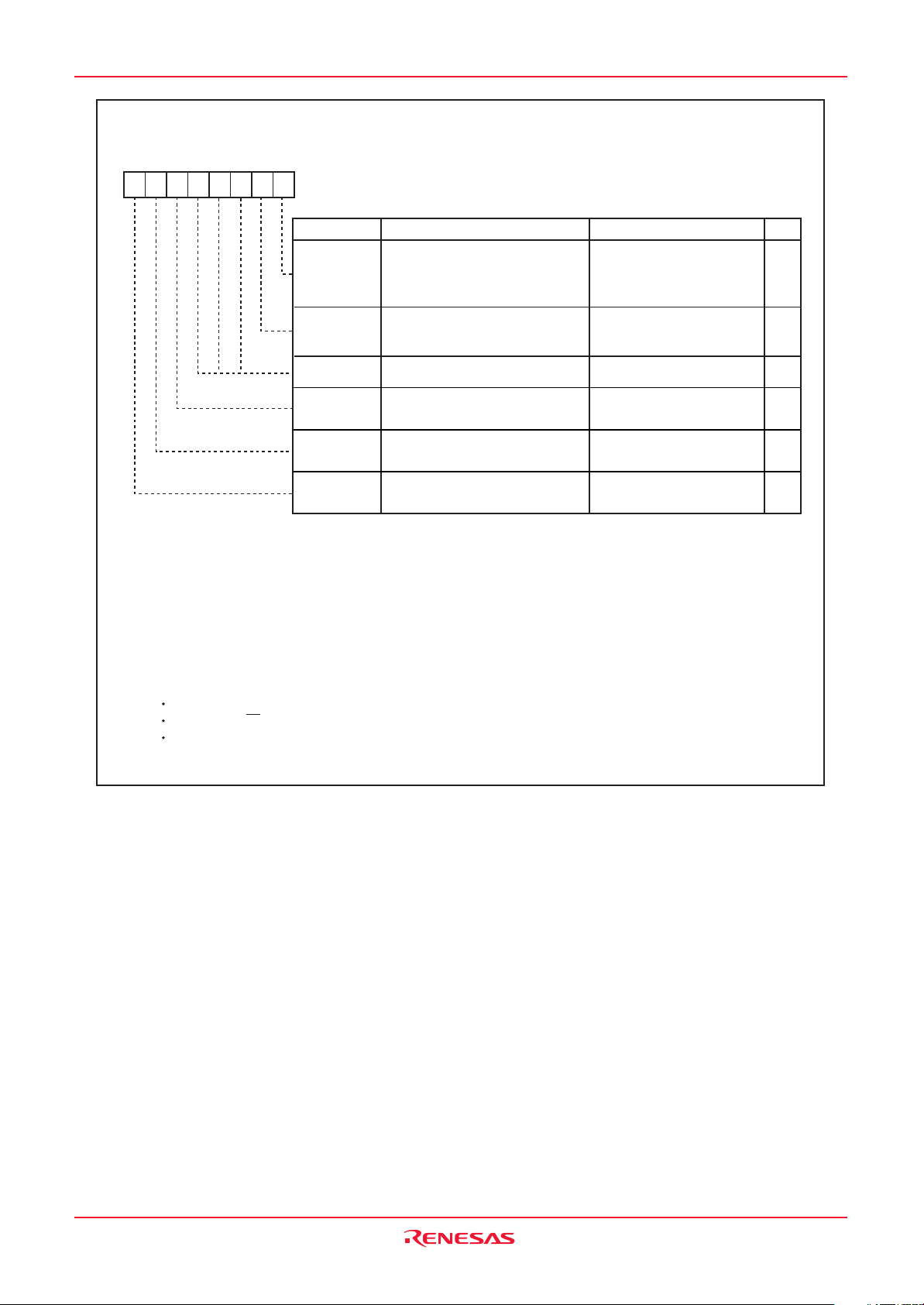
Under development
This document is under development and its contents are subject to change.
M16C/6N Group (M16C/6NL, M16C/6NN) 7. Clock Generating Circuit
Peripheral Clock Select Register
b7 b6 b5 b4 b3 b2 b1 b0
000
Symbol Address After Reset
PCLKR 025Eh 00h
(1)
Bit Name FunctionBit Symbol
Timers A, B, and A/D Clock
PCLK0
Select Bit
(Clock source for the timers A, B,
the dead time timer and A/D)
SI/O Clock Select Bit
PCLK1
-
(b4-b2)
PCLK5
PCLK6
PCLK7
(Clock source for UART0 to UART2,
SI/O3 to SI/O6)
(5)
Reserved Bit
Pin Function Swirch Bit
Software Interrupt Number/SFR
Location Switch Bit
A/D Clock Direct Input Bit
NOTES:
1. Write to this register after setting the PRC0 bit in the PRCR register to "1" (write enable).
2. If this bit is set to "1", the software interrupt number and SFR location can be changed as follows.
(1) Software interrupt number of the key input interrupt in the vector table can be changed from 14 to 13.
- No.13 is changed from the CAN0 error interrupt to the CAN0 error/key input interrupt.
- No.14 is changed from the A/D/key input interrupt to the A/D interrupt.
(2) Address of the KUPIC register in the SFR can be changed from 004Eh to 004Dh.
- Address 004Dh is changed from the C01ERRIC register to the C01ERRIC/KUPIC register.
- Address 004Eh is changed from the ADIC/KUPIC register to the ADIC register.
3. When this bit = 1, the A/D clock is set to divide-by-1 of fAD mode regardless of whether the PCLK0 bit is set.
4. When the PCLK5 bit and the SM43 bit in the S4C register = 1, the pin function of SI/O4 can be changed as follows.
P8_0/TA4OUT/U/(SIN4)
P7_5/TA2IN/W/(SOUT4)
P7_4/TA2OUT/W/(CLK4)
5. SI/O5 and SI/O6 are only in the 128-pin version.
0 : Divide-by-2 of fAD, f2
1 : fAD, f1
0 : f2SIO
1 : f1SIO
Set to "0"
0: Normal mode
1: Swiching mode
0: Normal mode
1: Swiching mode
0: Normal mode
1: Swiching mode
(4)
(2)
(3)
RW
RW
RW
RW
RW
RW
RW
Figure 7.5 PCLKR Register
Rev.1.02 Jul 01, 2005 page 36 of 314
REJ09B0126-0102
Page 53
Under development
This document is under development and its contents are subject to change.
M16C/6N Group (M16C/6NL, M16C/6NN) 7. Clock Generating Circuit
CAN0 Clock Select Register
b7 b6 b5 b4 b3 b2 b1 b0
1000
(1)
Symbol Address After Reset
CCLKR 025Fh 00h
Bit Name FunctionBit Symbol
b2 b1 b0
CCLK0
CCLK1
CAN0 Clock Select Bits
CCLK2
CCLK3
-
(b6-b4)
-
(b7)
CAN0 CPU Interface
Sleep Bit
(3)
Reserved Bit
Reserved Bit
NOTES:
1. Write to this register after setting the PRC0 bit in the PRCR register to "1" (Write enabled).
2. Set to this bit after setting the C1CTLR register to "0020h", and set only when the Reset bit in the C0CTLR
register = 1 (Reset/Initialization mode).
3. Before setting this bit to "1", set the Sleep bit in the C0CTLR register to "1" (Sleep mode enabled).
0 0 0 No division
0 0 1 : Divide-by-2
0 1 0 : Divide-by-4
(2)
0 1 1 : Divide-by-8
1 0 0: Divide-by-16
1 0 1 :
1 1 0 : Do not set a value
1 1 1 :
0: CAN0 CPU interface operating
1: CAN0 CPU interface in sleep
Set to
"0"
Set to
"1"
RW
RW
RW
RW
RW
RW
RW
Figure 7.6 CCLKR Register
Processor Mode Register 2
b7 b6 b5 b4 b3 b2 b1 b0
000
NOTES:
1. Write to this register after setting the PRC1 bit in the PRCR register to "1" (write enable).
2. The PM20 bit become effective when the PLC07 bit in the PLC0 register is set to "1" (PLL on). Change the PM20
bit when the PLC07 bit is set to "0" (PLL off). Set the PM20 bit t "0" (2 waits) when PLL clock > 16MHz.
3. Once this bit is set to "1", it cannot be set to "0" in a program.
4. Setting the PM22 bit to "1" results in the following conditions:
The on-chip oscillator starts oscillating, and the on-chip oscillator clock becomes the watchdog timer count source.
The CM10 bit in the CM1 register is disabled against write. (Writing a "1" has no effect, nor is stop mode entered.)
The watchdog timer does not stop when in wait mode or hold state.
(1)
Symbol Address After Reset
PM2 001Eh XXX00000b
Bit Symbol
Bit Name Function
Specifying Wait when
PM20
-
(b1)
PM22
-
(b4-b3)
-
(b7-b5)
Accessing SFR at PLL
Operation
(2)
Reserved Bit Set to "0"
WDT Count Source
Protective Bit
(3) (4)
Reserved Bit
Nothing is assigned. When write, set to "0".
When read, their contents are indeterminate.
0 : 2 waits
1 : 1 wait
0 : CPU clock is used for the
watchdog timer count source
1 : On-chip oscillator clock is used for
the watchdog timer count source
Set to "0"
RW
RW
RW
RW
RW
-
Figure 7.7 PM2 Register
Rev.1.02 Jul 01, 2005 page 37 of 314
REJ09B0126-0102
Page 54

Under development
This document is under development and its contents are subject to change.
M16C/6N Group (M16C/6NL, M16C/6NN) 7. Clock Generating Circuit
PLL Control Register 0
b7 b6 b5 b4 b3 b2 b1 b0
0 10
(1)
Symbol Address After Reset
PLC0 001Ch 0001X010b
Function
Do not set a value
PLC00
PLC01
PLC02
-
(b3)
-
(b4)
-
(b6-b5)
PLC07
Bit NameBit Symbol
b2 b1 b0
0 0 0 : Do not set a value
0 0 1 : Multiply by 2
PLL Multiplying Factor
Select Bit
(2)
0 1 0 : Multiply by 4
0 1 1 : Multiply by 6
1 0 0 :
1 0 1 :
1 1 0 :
1 1 1 :
Nothing is assigned. When write, set to "0".
When read, its content is indeterminate.
Reserved Bit Set to "1"
Reserved Bit Set to "0"
0 : PLL Off
Operation Enable Bit
(3)
1 : PLL On
NOTES:
1. Write to this register after setting the PRC0 bit in the PRCR register to "1" (write enable).
2. This bit can only be modified when the PLC07 bit = 0 (PLL turned off). The value once written to this bit
cannot be modified.
3. Before setting this bit to "1", set the CM07 bit in the CM0 register to "0" (main clock), set the CM17 to
CM16 bits in the CM1 register to "00b" (main clock undivided mode), and set the CM06 bit in the CM0
register to "0" (CM16 and CM17 bits enable).
RW
RW
RW
RW
-
RW
RW
RW
Figure 7.8 PLC0 Register
Rev.1.02 Jul 01, 2005 page 38 of 314
REJ09B0126-0102
Page 55

Under development
p
This document is under development and its contents are subject to change.
M16C/6N Group (M16C/6NL, M16C/6NN) 7. Clock Generating Circuit
The following describes the clocks generated by the clock generating circuit.
7.1.1 Main Clock
The main clock is generated by the main clock oscillation circuit. This clock is used as the clock source for
the CPU and peripheral function clocks. The main clock oscillator circuit is configured by connecting a
resonator between the XIN and XOUT pins. The main clock oscillator circuit contains a feedback resistor,
which is disconnected from the oscillator circuit during stop mode in order to reduce the amount of power
consumed in the chip. The main clock oscillator circuit may also be configured by feeding an externally
generated clock to the XIN pin. Figure 7.9 shows the examples of main clock connection circuit.
After reset, the main clock divided by 8 is selected for the CPU clock.
The power consumption in the chip can be reduced by setting the CM05 bit in the CM0 register to “1”
(main clock oscillator circuit turned off) after switching the clock source for the CPU clock to a sub clock or
on-chip oscillator clock. In this case, XOUT goes “H”. Furthermore, because the internal feedback resis-
tor remains on, XIN is pulled “H” to XOUT via the feedback resistor. Note, that if an externally generated
clock is fed into the XIN pin, the main clock cannot be turned off by setting the CM05 bit to “1” unless the
sub clock is selected as a CPU clock. If necessary, use an external circuit to turn off the clock.
During stop mode, all clocks including the main clock are turned off. Refer to 7.4 Power Control.
Microcomputer
(Built-in feedback resistor)
XIN XOUT XIN XOUT
(1)
Rd
CIN
NOTE:
1. Place a damping resistor if required. The resistance will vary depending on the oscillator
and the oscillation drive capacity setting. Use the value recommended by each
oscillator the oscillator manufacturer.
When the oscillation drive capacity is set to low, check that oscillation is stable.
Also, place a feedback resistor between XIN and XOUT if the oscillator manufacturer
recommends
lacing the resistor externally.
COUT
Figure 7.9 Examples of Main Clock Connection Circuit
Microcomputer
(Built-in feedback resistor)
Open
Externally derived clock
VCC
VSS
Rev.1.02 Jul 01, 2005 page 39 of 314
REJ09B0126-0102
Page 56

Under development
This document is under development and its contents are subject to change.
M16C/6N Group (M16C/6NL, M16C/6NN) 7. Clock Generating Circuit
7.1.2 Sub Clock
The sub clock is generated by the sub clock oscillation circuit. This clock is used as the clock source for
the CPU clock, as well as the timer A and timer B count sources. In addition, an fC clock with the same
frequency as that of the sub clock can be output from the CLKOUT pin.
The sub clock oscillator circuit is configured by connecting a crystal resonator between the XCIN and
XCOUT pins. The sub clock oscillator circuit contains a feedback resistor, which is disconnected from the
oscillator circuit during stop mode in order to reduce the amount of power consumed in the chip. The sub
clock oscillator circuit may also be configured by feeding an externally generated clock to the XCIN pin.
Figure 7.10 shows the examples of sub clock connection circuit.
After reset, the sub clock is turned off. At this time, the feedback resistor is disconnected from the oscilla-
tor circuit.
To use the sub clock for the CPU clock, set the CM07 bit in the CM0 register to “1 ” (sub clock) after the
sub clock becomes oscillating stably.
During stop mode, all clocks including the sub clock are turned off. Refer to 7.4 Power Control.
Microcomputer
(Built-in feedback resistor)
XCIN XCOUT XCIN XCOUT
(1)
RCd
CCIN
NOTE:
1. Place a damping resistor if required. The resistance will vary depending on the oscillator
and the oscillation drive capacity setting. Use the value recommended by each
oscillator the oscillator manufacturer.
When the oscillation drive capacity is set to low, check that oscillation is stable.
Also, place a feedback resistor between XCIN and XCOUT if the oscillator manufacturer
recommends placing the resistor externally.
CCOUT
Figure 7.10 Examples of Sub Clock Connection Circuit
Microcomputer
(Built-in feedback resistor)
Open
Externally derived clock
VCC
VSS
Rev.1.02 Jul 01, 2005 page 40 of 314
REJ09B0126-0102
Page 57

Under development
This document is under development and its contents are subject to change.
M16C/6N Group (M16C/6NL, M16C/6NN) 7. Clock Generating Circuit
7.1.3 On-chip Oscillator Clock
This clock, approximately 1 MHz, is supplied by a on-chip oscillator. This clock is used as the clock
source for the CPU and peripheral function clocks. In addition, if the PM22 bit in the PM2 register is “1”
(on-chip oscillator clock for the watchdog timer count source), this clock is used as the count source for
the watchdog timer (refer to 10.1 Count Source Protective Mode).
After reset, the on-chip oscillator is turned off. It is turned on by setting the CM21 bit in the CM2 register
to “1” (on-chip oscillator clock), and is used as the clock source for the CPU and peripheral function
clocks, in place of the main clock. If the main clock stops oscillating when the CM20 bit in the CM2 register
is “1” (oscillation stop, re-oscillation detection function enabled) and the CM27 bit is “1” (oscillation stop,
re-oscillation detection interrupt), the on-chip oscillator automatically starts operating, supplying the nec-
essary clock for the microcomputer.
7.1.4 PLL Clock
The PLL clock is generated by a PLL frequency synthesizer. This clock is used as the clock source for the
CPU and peripheral function clocks. After reset, the PLL clock is turned off. The PLL frequency synthe-
sizer is activated by setting the PLC07 bit to “1” (PLL operation). When the PLL clock is used as the clock
source for the CPU clock, wait a fixed period of tsu(PLL) for the PLL clock to be stable, and then set the
CM11 bit in the CM1 register to “1”.
Before entering wait mode or stop mode, be sure to set the CM11 bit to “0” (CPU clock source is the main
clock). Furthermore, before entering stop mode, be sure to set the PLC07 bit in the PLC0 register to “0”
(PLL stops). Figure 7.11 shows the procedure for using the PLL clock as the clock source for the CPU.
The PLL clock frequency is determined by the equation below.
PLL clock frequency = f(XIN) ✕ (multiplying factor set by the PLC02 to PLC00 bits in the PLC0 register)
(However, PLL clock frequency = 16 MHz, 20 MHz or 24 MHz)
The PLC02 to PLC00 bits can be set only once after reset. Table 7.2 shows the example for setting PLL
clock frequencies.
Table 7.2 Example for Setting PLL Clock Frequencies
XIN
(MHz)
8
4
10
5
12
6
4
PLC02
0
0
0
0
0
0
0
PLC01 PLC00
0
1
0
1
0
1
1
1
0
1
0
1
0
1
Multiply
Factor
2
4
2
4
2
4
6
PLL Clock
(1)
(MHz)
16
20
24
NOTE:
1. PLL clock frequency = 16 MHz , 20 MHz or 24 MHz
Rev.1.02 Jul 01, 2005 page 41 of 314
REJ09B0126-0102
Page 58

Under development
This document is under development and its contents are subject to change.
M16C/6N Group (M16C/6NL, M16C/6NN) 7. Clock Generating Circuit
Using the PLL clock as the clock source for the CPU
Set the CM07 bit to "0" (main clock), the CM17 to CM16
bits to "00b" (main clock undivided), and the CM06 bit to "0"
(CM16 and CM17 bits enabled).
(1)
Set the PLC02 to PLC00 bits (multiplying factor).
(When PLL clock > 16 MHz)
Set the PM20 bit to "0" (2-wait state).
Set the PLC07 bit to "1" (PLL operation).
Wait until the PLL clock becomes stable (tsu(PLL)).
Set the CM11 bit to "1" (PLL clock for the CPU clock source).
END
NOTE:
1. PLL operation mode can be entered from high-speed mode.
Figure 7.11 Procedure to Use PLL Clock as CPU Clock Source
Rev.1.02 Jul 01, 2005 page 42 of 314
REJ09B0126-0102
Page 59

Under development
This document is under development and its contents are subject to change.
M16C/6N Group (M16C/6NL, M16C/6NN) 7. Clock Generating Circuit
7.2 CPU Clock and Peripheral Function Clock
Two type clocks: CPU clock to operate the CPU and peripheral function clocks to operate the peripheral
functions.
7.2.1 CPU Clock and BCLK
These are operating clocks for the CPU and watchdog timer.
The clock source for the CPU clock can be chosen to be the main clock, sub clock, on-chip oscillator clock
or the PLL clock.
If the main clock or on-chip oscillator clock is selected as the clock source for the CPU clock, the selected
clock source can be divided by 1 (undivided), 2, 4, 8 or 16 to produce the CPU clock. Use the CM06 bit in
the CM0 register and the CM17 to CM16 bits in the CM1 register to select the divide-by-n value.
When the PLL clock is selected as the clock source for the CPU clock, the CM06 bit should be set to “0”
and the CM17 to CM16 bits to “00b” (undivided).
After reset, the main clock divided by 8 provides the CPU clock.
Note that when entering stop mode from high- or medium-speed mode, on-chip oscillator mode or on-chip
oscillator low power dissipation mode, or when the CM05 bit in the CM0 register is set to “1” (main clock
turned off) in low-speed mode, the CM06 bit in the CM0 register is set to “1” (divide-by-8 mode).
7.2.2 Peripheral Function Clock (f1, f2, f8, f32, f1SIO, f2SIO, f8SIO, f32SIO, fAD, fCAN0, fC32)
These are operating clocks for the peripheral functions.
Two of these, fi (i = 1, 2, 8, 32) and fiSIO are derived from the main clock, PLL clock or on-chip oscillator
clock by dividing them by i. The clock fi is used for timers A and B, and fiSIO is used for serial I/O. The f8
and f32 clocks can be output from the CLKOUT pin.
The fAD clock is produced from the main clock, PLL clock or on-chip oscillator clock, and is used for the
A/D converter.
The fCAN0 clock is derived from the main clock, PLL clock or on-chip oscillator clock by dividing them by
1 (undivided), 2, 4, 8 or 16, and is used for the CAN module.
When the WAIT instruction is executed after setting the CM02 bit in the CM0 register to “1” (peripheral
function clock turned off during wait mode), or when the microcomputer is in low power dissipation mode,
the fi, fiSIO, fAD, and fCAN0 clocks are turned off
(1)
.
The fC32 clock is derived from the sub clock, and is used for timers A and B. This clock can be used when
the sub clock is activated.
NOTE
1. fCAN0 clock stops at “H” in CAN0 sleep mode.
7.3 Clock Output Function
The f8, f32 or fC clock can be output from the CLKOUT pin. Use the CM01 to CM00 bits in the CM0 register
to select.
Rev.1.02 Jul 01, 2005 page 43 of 314
REJ09B0126-0102
Page 60

Under development
This document is under development and its contents are subject to change.
M16C/6N Group (M16C/6NL, M16C/6NN) 7. Clock Generating Circuit
7.4 Power Control
Normal operation mode, wait mode and stop mode are provided as the power consumption control.
All mode states, except wait mode and stop mode, are called normal operation mode in this document.
7.4.1 Normal Operation Mode
Normal operation mode is further classified into seven sub modes.
In normal operation mode, because the CPU clock and the peripheral function clocks both are on, the
CPU and the peripheral functions are operating. Power control is exercised by controlling the CPU clock
frequency. The higher the CPU clock frequency, the greater the processing capability. The lower the CPU
clock frequency, the smaller the power consumption in the chip. If the unnecessary oscillator circuits are
turned off, the power consumption is further reduced.
Before the clock sources for the CPU clock can be switched over, the new clock source to which switched
must be oscillating stably. If the new clock source is the main clock, sub clock or PLL clock, allow a
sufficient wait time in a program until it becomes oscillating stably.
Note that operation modes cannot be changed directly from low-speed or low power dissipation mode to
on-chip oscillator or on-chip oscillator low power dissipation mode. Nor can operation modes be changed
directly from on-chip oscillator or on-chip oscillator low power dissipation mode to low-speed or low power
dissipation mode. Where the CPU clock source is changed from the on-chip oscillator to the main clock,
change the operation mode to the medium-speed mode (divide-by-8 mode) after the clock was divided by
8 (the CM06 bit in the CM0 register was set to “1”) in the on-chip oscillator mode.
7.4.1.1 High-speed Mode
The main clock divided by 1 provides the CPU clock. If the sub clock is activated, fC32 can be used as
the count source for timers A and B.
7.4.1.2 PLL Operation Mode
The main clock multiplied by 2, 4 or 6 provides the PLL clock, and this PLL clock serves as the CPU
clock. If the sub clock is activated, fC32 can be used as the count source for timers A and B. PLL
operation mode can be entered from high speed mode. If PLL operation mode is to be changed to wait
or stop mode, first go to high speed mode before changing.
7.4.1.3 Medium-speed Mode
The main clock divided by 2, 4, 8 or 16 provides the CPU clock. If the sub clock is activated, fC32 can be
used as the count source for timers A and B.
7.4.1.4 Low-speed Mode
The sub clock provides the CPU clock. The main clock is used as the clock source for the peripheral
function clock when the CM21 bit in the CM2 register is set to “0” (on-chip oscillator turned off), and the
on-chip oscillator clock is used when the CM21 bit is set to “1” (on-chip oscillator oscillating).
The fC32 clock can be used as the count source for timers A and B.
7.4.1.5 Low Power Dissipation Mode
In this mode, the main clock is turned off after being placed in low speed mode. The sub clock provides
the CPU clock. The fC32 clock can be used as the count source for timers A and B.
Simultaneously when this mode is selected, the CM06 bit in the CM0 register becomes “1” (divide-by-8
mode). In the low power dissipation mode, do not change the CM06 bit. Consequently, the medium
speed (divide-by-8) mode is to be selected when the main clock is operated next.
Rev.1.02 Jul 01, 2005 page 44 of 314
REJ09B0126-0102
Page 61

Under development
This document is under development and its contents are subject to change.
M16C/6N Group (M16C/6NL, M16C/6NN) 7. Clock Generating Circuit
7.4.1.6 On-chip Oscillator Mode
The on-chip oscillator clock divided by 1 (undivided), 2, 4, 8 or 16 provides the CPU clock. The on-chip
oscillator clock is also the clock source for the peripheral function clocks. If the sub clock is activated,
fC32 can be used as the count source for timers A and B.
7.4.1.7 On-chip Oscillator Low Power Dissipation Mode
The main clock is turned off after being placed in on-chip oscillator mode. The CPU clock can be
selected like in the on-chip oscillator mode. The on-chip oscillator clock is the clock source for the
peripheral function clocks. If the sub clock is activated, fC32 can be used as the count source for timers
A and B. When the operation mode is returned to the high- and medium-speed modes, set the CM06 bit
in the CM0 register to “1” (divide-by-8 mode).
Table 7.3 lists the setting clock related bit and modes.
Table 7.3 Setting Clock Related Bit and Modes
Modes
CM2 Register
CM21 CM11
CM1 Register CM0 Register
CM17, CM16
CM07 CM06 CM05 CM04
PLL Operation Mode 0 1 0 0b 0 0 0 -
High-Speed Mode 0 0 00b 0 0 0 -
Medium-
Speed
Mode
divided by 2
divided by 4
divided by 8
divided by 16
0 0 01b 0 0 0 -
0 0 10b 0 0 0 -
00-0 10-
0 0 11b 0 0 0 -
Low-Speed Mode - 0 - 1 - 0 1
Low Power 0 0 - 1 1
(1)
1
(1)
1
Dissipation Mode
On-chip
Oscillator
Mode
divided by 1
divided by 2
divided by 4
divided by 8
divided by 16
1 0 00b 0 0 0 -
1 0 01b 0 0 0 -
1 0 10b 0 0 0 -
10-0 10-
1 0 11b 0 0 0 -
On-chip Oscillator 1 0 (NOTE 2) 0 (NOTE 2) 1 Low power Dissipation
Mode
-: “0” or “1”
NOTES:
1. When the CM05 bit is set to “1” (main clock turned off) in low-speed mode, the mode goes to low power
dissipation mode and the CM06 bit is set to “1” (divide-by-8 mode) simultaneously.
2. The divide-by-n value can be selected the same way as in on-chip oscillator mode.
Rev.1.02 Jul 01, 2005 page 45 of 314
REJ09B0126-0102
Page 62

Under development
This document is under development and its contents are subject to change.
M16C/6N Group (M16C/6NL, M16C/6NN) 7. Clock Generating Circuit
7.4.2 Wait Mode
In wait mode, the CPU clock is turned off, so are the CPU (because operated by the CPU clock) and the
watchdog timer. However, if the PM22 bit in the PM2 register is “1” (on-chip oscillator clock for the watchdog
timer count source), the watchdog timer remains active. Because the main clock, sub clock and on-chip
oscillator clock all are on, the peripheral functions using these clocks keep operating.
7.4.2.1 Peripheral Function Clock Stop Function
If the CM02 bit in the CM0 register is “1” (peripheral function clocks turned off during wait mode), the f1,
f2, f8, f32, f1SIO, f8SIO, f32SIO, fAD and fCAN0 clocks are turned off when in wait mode, with the power
consumption reduced that much. However, fC32 remains on.
7.4.2.2 Entering Wait Mode
The microcomputer is placed into wait mode by executing the WAIT instruction.
When the CM11 bit = 1 (CPU clock source is the PLL clock), be sure to set the CM11 bit in the CM1
register to “0” (CPU clock source is the main clock) before going to wait mode. The power consumption
of the chip can be reduced by setting the PLC07 bit in the PLC0 register to “0” (PLL stops).
7.4.2.3 Pin Status During Wait Mode
Table 7.4 lists the pin status during wait mode.
Table 7.4 Pin Status During Wait Mode
Pin Single-Chip Mode
I/O Ports Retains status before wait mode
CLKOUT Does not stop
When fC selected
When f8, f32 selected
•CM02 bit = 0: Does not stop
•CM02 bit = 1: Retains status before wait mode
7.4.2.4 Exiting Wait Mode
______
The microcomputer is moved out of wait mode by a hardware reset, NMI interrupt or peripheral function
interrupt.
______
If the microcomputer is to be moved out of wait mode by a hardware reset or NMI interrupt, set the
peripheral function interrupt priority ILVL2 to ILVL0 bits to “000b” (interrupt disabled) before executing
the WAIT instruction.
The peripheral function interrupts are affected by the CM02 bit. If the CM02 bit is “0” (peripheral function
clocks not turned off during wait mode), peripheral function interrupts can be used to exit wait mode. If
the CM02 bit is “1” (peripheral function clocks turned off during wait mode), the peripheral functions
using the peripheral function clocks stop operating, so that only the peripheral functions clocked by
external signals can be used to exit wait mode.
Table 7.5 lists the interrupts to exit wait mode.
Rev.1.02 Jul 01, 2005 page 46 of 314
REJ09B0126-0102
Page 63

Under development
This document is under development and its contents are subject to change.
M16C/6N Group (M16C/6NL, M16C/6NN) 7. Clock Generating Circuit
Table 7.5 Interrupts to Exit Wait Mode
_______
Interrupt CM02 Bit = 0 CM02 Bit = 1
NMI Interrupt Can be used Can be used
Serial I/O Interrupt Can be used when operating with Can be used when operating with
internal or external clock external clock
Key Input Interrupt Can be used Can be used
A/D Conversion Interrupt Can be used in one-shot mode or - (Do not use)
single sweep mode
Timer A Interrupt Can be used in all modes Can be used in event counter mode
Timer B interrupt or when the count source is fc32
______
INT Interrupt Can be used Can be used
CAN0 Wake-up Interrupt Can be used in CAN sleep mode Can be used in CAN sleep mode
If the microcomputer is to be moved out of wait mode by a peripheral function interrupt, set up the
following before executing the WAIT instruction.
(1) Set the ILVL2 to ILVL0 bits in the interrupt control register, for peripheral function interrupts used to
exit wait mode.
The ILVL2 to ILVL0 bits in all other interrupt control registers, for peripheral function interrupts not
used to exit wait mode, are set to “000b” (interrupt disable).
(2) Set the I flag to “1”.
(3) Start operating the peripheral functions used to exit wait mode.
When the peripheral function interrupt is used, an interrupt routine is performed as soon as an
interrupt request is acknowledged and the CPU clock is supplied again.
When the microcomputer exits wait mode by the peripheral function interrupt, the CPU clock is the same
clock as the CPU clock executing the WAIT instruction.
Rev.1.02 Jul 01, 2005 page 47 of 314
REJ09B0126-0102
Page 64

Under development
This document is under development and its contents are subject to change.
M16C/6N Group (M16C/6NL, M16C/6NN) 7. Clock Generating Circuit
7.4.3 Stop Mode
In stop mode, all oscillator circuits are turned off, so are the CPU clock and the peripheral function clocks.
Therefore, the CPU and the peripheral functions clocked by these clocks stop operating. The least
amount of power is consumed in this mode. If the voltage applied to VCC is VRAM or more, the internal
RAM is retained.
However, the peripheral functions clocked by external signals keep operating. The following interrupts
can be used to exit stop mode.
7.4.3.1 Entering Stop Mode
______
• NMI interrupt
• Key interrupt
______
• INT interrupt
• Timer A, Timer B interrupt (when counting external pulses in event counter mode)
• Serial I/O interrupt (when external clock is selected)
• CAN0 Wake-up interrupt (when CAN sleep mode is selected)
The microcomputer is placed into stop mode by setting the CM10 bit in the CM1 register to “1” (all clocks
turned off). At the same time, the CM06 bit in the CM0 register is set to “1” (divide-by-8 mode) and the
CM15 bit in the CM1 register is set to “1” (main clock oscillator circuit drive capability high).
Before entering stop mode, set the CM20 bit in the CM2 register to “0” (oscillation stop, re-oscillation
detection function disabled).
Also, if the CM11 bit in the CM1 register is “1” (PLL clock for the CPU clock source), set the CM11 bit to
“0” (main clock for the CPU clock source) and the PLC07 bit in the PLC0 register to “0” (PLL turned off)
before entering stop mode.
7.4.3.2 Pin Status in Stop Mode
Table 7.6 lists the pin status in stop mode.
Table 7.6 Pin Status in Stop Mode
Pin Single-Chip Mode
I/O Ports Retains status before stop mode
CLKOUT “H”
When fC selected
When f8, f32 selected
Retains status before stop mode
Rev.1.02 Jul 01, 2005 page 48 of 314
REJ09B0126-0102
Page 65

Under development
This document is under development and its contents are subject to change.
M16C/6N Group (M16C/6NL, M16C/6NN) 7. Clock Generating Circuit
7.4.3.3 Exiting Stop Mode
Stop mode is exited by a hardware reset, NMI interrupt or peripheral function interrupt.
_______
_______
When the hardware reset or NMI interrupt is used to exit wait mode, set all ILVL2 to ILVL0 bits in the
interrupt control registers for the peripheral function interrupt to “000b” (interrupt disabled) before setting
the CM10 bit in the CM1 register to “1”.
When the peripheral function interrupt is used to exit stop mode, set the CM10 bit to “1” after the following
settings are completed.
(1) The ILVL2 to ILVL0 bits in the interrupt control registers, for the peripheral function interrupt used to
exit stop mode, must have larger value than that of the RLVL2 to RLVL0 bits.
The ILVL2 to ILVL0 bits in all other interrupt control registers, for the peripheral function interrupts
which are not used to exit stop mode, must be set to “000b” (interrupt disabled).
(2) Set the I flag to “1”.
(3) Start operation of peripheral function being used to exit wait mode.
When exiting stop mode by the peripheral function interrupt, the interrupt routine is performed when
an interrupt request is generated and the CPU clock is supplied again.
_______
When stop mode is exited by the peripheral function interrupt or NMI interrupt, the CPU clock source is
as follows, in accordance with the CPU clock source setting before the microcomputer had entered stop
mode.
• When the sub clock is the CPU clock before entering stop mode: Sub clock
• When the main clock is the CPU clock source before entering stop mode: Main clock divided by 8
• When the on-chip oscillator clock is the CPU clock source before entering stop mode:
On-chip oscillator clock divided by 8
Rev.1.02 Jul 01, 2005 page 49 of 314
REJ09B0126-0102
Page 66
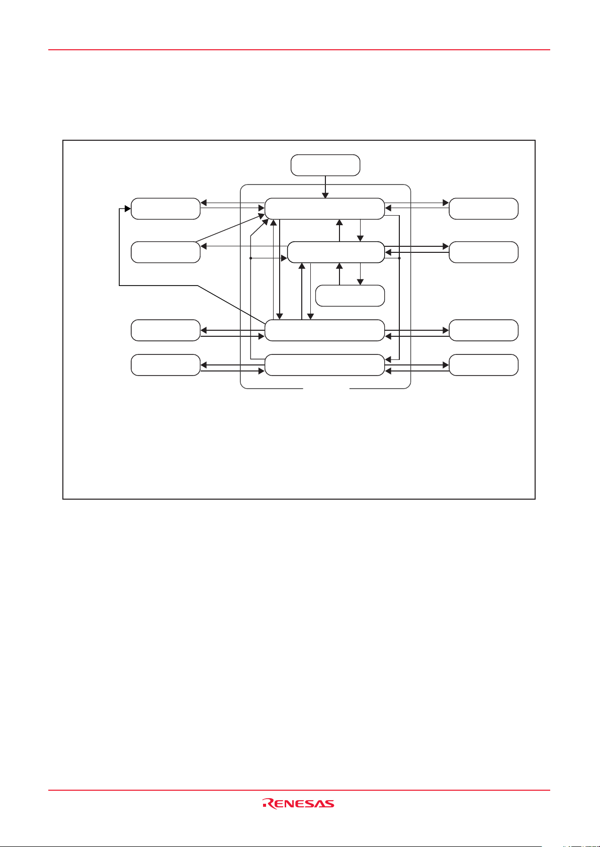
Under development
This document is under development and its contents are subject to change.
M16C/6N Group (M16C/6NL, M16C/6NN) 7. Clock Generating Circuit
Figure 7.12 shows the state transition from normal operation mode to stop mode and wait mode. Figure
7.13 shows the state transition in normal operation mode.
Table 7.7 shows a state transition matrix describing allowed transition and setting. The vertical line shows
current state and horizontal line show state after transition.
Reset
CPU operation stoppedAll oscillators stopped
Wait Mode
Wait Mode
Wait Mode
Wait Mode
CM07 = 0
CM06 = 1
CM05 = 0
CM11 = 0
CM10 = 1
(5)
CM10 = 1
Stop Mode
(3)
Stop Mode
Stop Mode
Stop Mode
Interrupt
Interrupt
CM10 = 1
CM10 = 1
Interrupt
CM10 = 1
Interrupt
(5)
(5)
(5)
(4)
When
power
dissipation
mode
Medium-Speed Mode
(divided-by-8 mode)
High-Speed Mode,
Medium-Speed Mode
When
low
low-
speed
mode
PLL Operation Mode
Low-Speed Mode,
Low Power Dissipation Mode
On-chip Oscillator Mode,
On-chip Oscillator Dissipation Mode
(NOTES 1, 2)
WAIT
instruction
Interrupt
WAIT
instruction
Interrupt
WAIT
instruction
Interrupt
WAIT
instruction
Interrupt
Normal Mode
CM05, CM06, CM07: Bits in CM0 register
CM10, CM11: Bits in CM1 register
NOTES:
Do not go directly from PLL operation mode to wait or stop mode.
1.
2.PLL operation mode can be entered from high-speed mode. Similarly, PLL operation mode can be changed back to high-speed mode.
3.Write to the CM0 and CM1 registers per 16 bits with the CM21 bit in the CM2 register = 0 (on-chip oscillator stops).
Since the operation starts from the main clock after exiting stop mode, the time until the CPU operates can be reduced.
4.The on-chip oscillator clock divided by 8 provides the CPU clock.
5. Before entering stop mode, be sure to set the CM20 bit in the CM2 register to "0" (oscillation stop, re-oscillation detection function disabled).
Figure 7.12 State Transition to Stop Mode and Wait Mode
Rev.1.02 Jul 01, 2005 page 50 of 314
REJ09B0126-0102
Page 67

Under development
This document is under development and its contents are subject to change.
M16C/6N Group (M16C/6NL, M16C/6NN) 7. Clock Generating Circuit
Main Clock Oscillation
PLL operation mode
: f(PLL)
: f(PLL)
PLC07 = 1
CM11 = 1
PLC07 = 0
CM11 = 0
PLC07 = 1
CM11 = 1
PLC07 = 0
CM11 = 0
CPU clock
CM07 = 0
CM06 = 0
CM17 = 0
CM16 = 0
CPU clock
CM07 = 0
CM06 = 0
CM17 = 0
CM16 = 0
PLL operation mode
High-Speed Mode
CPU clock
(6)
CM07 = 0
CM06 = 0
CM17 = 0
(7)
CM16 = 0
High-Speed mode
CPU clock
(6)
CM07 = 0
CM06 = 0
CM17 = 0
(7)
CM16 = 0
: f(XIN)
: f(XIN)
Medium-Speed Mode
(divide by 2)
CPU clock
: f(XIN)/2
CM07 = 0
CM06 = 0
CM17 = 0
CM16 = 1
Medium-Speed Mode
(divide by 2)
CPU clock
: f(XIN)/2
CM07 = 0
CM06 = 0
CM17 = 0
CM16 = 1
Medium-Speed Mode
(divide by 4)
CPU clock
: f(XIN)/4
CM07 = 0
CM06 = 0
CM17 = 1
CM16 = 0
CM04 = 1CM04 = 1 CM04 = 0 CM04 = 0
Medium-Speed Mode
(divide by 4)
CPU clock
: f(XIN)/4
CM07 = 0
CM06 = 0
CM17 = 1
CM16 = 0
(3)
CM07 =1
CPU clock: f(XCIN)
CM07 = 0
(1) (9)
CM05 = 1
Low Power Dissipation Mode
CPU clock: f(XCIN)
CM07 = 0
CM06 = 1
CM15 = 1
Medium-Speed Mode
(divide by 8)
CPU clock
: f(XIN)/8
CM07 = 0
CM06 = 1
Medium-Speed Mode
(divide by 8)
CPU clock
: f(XIN)/8
CM07 = 0
CM06 = 1
CM07 = 0
CM05 = 0
Medium-Speed Mode
Medium-Speed Mode
(2) (4)
(divide by 16)
CPU clock
: f(XIN)/16
CM07 = 0
CM06 = 0
CM17 = 1
CM16 = 1
(divide by 16)
CPU clock
: f(XIN)/16
CM07 = 0
CM06 = 0
CM17 = 1
CM16 = 1
CM21 = 0
CM21 = 1
CM21 = 0
CM21 = 1
CM21 = 0
CM21 = 1
On-chip Oscillator
Mode
CPU clock
(8)
f(Ring)
f(Ring)/2
f(Ring)/4
f(Ring)/8
f(Ring)/16
CM04 = 1
CM04 = 0
CPU clock
(8)
f(Ring)
f(Ring)/2
f(Ring)/4
f(Ring)/8
f(Ring)/16
On-chip Oscillator
Mode
Low-Speed ModeLow-Speed Mode
CPU clock: f(XCIN)
CM07 = 0
On-chip Oscillator
Clock Oscillation
On-chip Oscillator
Low Power Dissipation Mode
CPU clock
CM05 = 0
f(Ring)
f(Ring)/2
f(Ring)/4
(1)
CM05 = 1
f(Ring)/8
f(Ring)/16
CM04 = 1
CM04 = 0
CPU clock
CM05 = 0
f(Ring)
f(Ring)/2
f(Ring)/4
(1)
CM05 = 1
f(Ring)/8
f(Ring)/16
On-chip Oscillator
Low Power Dissipation Mode
Sub clock oscillation
CM04, CM05, CM06, CM07: Bits in CM0 register
CM11, CM15, CM16, CM17: Bits in CM1 register
CM20, CM21 : Bits in CM2 register
PLC07 : Bit in PLC0 register
NOTES:
1. Avoid making a transition when the CM20 bit is set to "1" (oscillation stop, re-oscillation detection function enabled).
Set the CM20 bit to "0" (oscillation stop, re-oscillation detection function disabled) before transiting.
2. Wait for the main clock oscillation stabilization time.
3. Switch clock after oscillation of sub clock is sufficiently stable.
4. Change the CM17 and CM16 bits before changing the CM06 bit.
5. Transit in accordance with arrow.
6. The PM20 bit in the PM2 register become effective when the PLC07 bit is set to "1" (PLL on). Change the PM20 bit when the PLC07 bit is
set to "0" (PLL off). Set the PM20 bit to "0" (2 waits) when PLL clock > 16 MHz.
PM20 bit to "0" (SFR accessed with two wait states) before setting the PLC07 bit to "1" (PLL operation).
7. PLL operation mode can only be changed to high-speed mode.
8. Set the CM06 bit to "1" (division by 8 mode) before changing back the operation mode from on-chip oscillator mode to high- or middle-speed mode.
9. When the CM21 bit = 0 (on-chip oscillator turned off) and the CM05 bit = 1 (main clock turned off), the CM06 bit is fixed to "1" (divide-by-8 mode)
and the CM15 bit is fixed to "1" (drive capability High).
Figure 7.13 State Transition in Normal Operation Mode
Rev.1.02 Jul 01, 2005 page 51 of 314
REJ09B0126-0102
Page 68

Under development
This document is under development and its contents are subject to change.
M16C/6N Group (M16C/6NL, M16C/6NN) 7. Clock Generating Circuit
Table 7.7 Allowed Transition and Setting
State after transition
High-Speed Mode,
Medium-Speed Mode
Low-Speed
(2)
Mode
Low Power
Dissipation Mode
PLL Operation
(2)
Mode
On-chip Oscillator
Mode
Current state
On-chip Oscillator Low
Power Dissipation Mode
Stop Mode
High-Speed Mode,
Medium-Speed
Mode
(NOTE 8) (9)
Low-Speed Low Power
(2)
Mode
(7)
(8) (11)
-
(12)
(14)
(10)
(3)
(4)
-- ----
---
----
(5)
(18)
(18) (18)
PLL Operation
Dissipation Mode
-
Mode (2) Mode
(13)
(1) (6)
On-chip Oscillator
(3)
(15)
---
---
(NOTE 8) (11)
(10) (NOTE 8) (16)
-
(18)
On-chip Oscillator
Low Power
Dissipation Mode
-
(1)
(5)
(18)
(5)
Stop Wait
Mode Mode
(1)
(16)
(1)
(16)
(1)
(16)
(1)
(16)
(1)
(17)
(17)
(17)
(17)
(17)
-
Wait Mode
-: Cannot transit
NOTES:
1. Avoid making a transition when the CM20 bit = 1 (oscillation stop, reoscillation detection function enabled). Set the CM20 bit to “0” (oscillation
stop, re-oscillation detection function disabled) before transiting.
2. On-chip oscillator clock oscillates and stops in low-speed mode. In this
mode, the on-chip oscillator can be used as peripheral function clock. Sub
clock oscillates and stops in PLL operation mode. In this mode, sub clock
can be used as peripheral function clock.
3. PLL operation mode can only be entered from and changed to high-speed
mode.
4. Set the CM06 bit to “1” (division by 8 mode) before transiting from on-chip
oscillator mode to high- or medium-speed mode.
5. When exiting stop mode, the CM06 bit is set to “1” (division by 8 mode).
6. If the CM05 bit is set to “1” (main clock stop), then the CM06 bit is set to “1”
(division by 8 mode).
7. A transition can be made only when sub clock is oscillating.
8. State transitions within the same mode (divide-by-n values changed or sub
clock oscillation turned on or off) are shown in the table below.
(18) (18) (18)
Sub Clock Oscillating Sub Clock Turned Off
Divided Divided Divided DividedNoDivided Divided Divided Divided
No
Division
by 2 by 4 by 8 by 16
No Division
Divided by 2
Divided by 4
Divided by 8
Divided by 16
Sub Clock Oscillating
No Division
Divided by 2-(2)
Divided by 4
Divided by 8
Divided by 16
Sub Clock Turned Off
9. ( ):setting method. See right table.
(4) (5) (7) (6) (1)
(3) (5) (7) (6)
(3) (4) (7) (6)
(3) (4) (5) (6)
(3) (4) (5) (7)
(2)
----
---
--
(2)
---
----
--
(2)
Division
by 2 by 4 by 8 by 16
----
-
(1)
---
--
(1)
---
----
(4) (5) (7) (6)
(3) (5) (7) (6)
(3) (4) (7) (6)
-
(3) (4) (5) (6)
(2) (3) (4) (5) (7)
--
(1)
-
(18) (18)
-
Setting Operation
(1) CM04=0 Sub clock turned off
(2) CM04=1 Sub clock oscillating
(
3) CM06=0 CPU clock no division
CM17=0 mode
CM16=0
(
4) CM06=0
CPU clock division by 2
CM17=0 mode
CM16=1
(
5) CM06=0
CPU clock division by 4
CM17=1 mode
CM16=0
(
6) CM06=0
CPU clock division by 16
CM17=1 mode
CM16=1
(7) CM06=1
(8) CM07=0 Main clock, PLL clock
CPU clock division by 8 mode
or on-chip oscillator
clock selected
(9) CM07=1 Sub clock selected
(10)
CM05=0 Main clock oscillating
(11)
CM05=1 Main clock turned off
(12)
PLC07=0 Main clock selected
CM11=0
(
13)
PLC07=1 PLL clock selected
-
(1)
CM11=1
(14)
CM21=0 Main clock or
PLL clock selected
(
15)
CM21=1 On-chip oscillator clock
selected
(16)
CM10=1 Transition to stop mode
(17)
WAIT Transition to wait mode
instruction
(18)
Hardware Exit stop mode or wait
interrupt mode
CM04, CM05, CM06, CM07: Bits in CM0 register
CM10, CM11, CM16, CM17: Bits in CM1 register
CM20, CM21 : Bits in CM2 register
PLC07 : Bit in PLC0 register
Rev.1.02 Jul 01, 2005 page 52 of 314
REJ09B0126-0102
Page 69

Under development
This document is under development and its contents are subject to change.
M16C/6N Group (M16C/6NL, M16C/6NN) 7. Clock Generating Circuit
7.5 Oscillation Stop and Re-oscillation Detection Function
The oscillation stop and re-oscillation detection function is such that main clock oscillation circuit stop and
re-oscillation are detected. At oscillation stop, re-oscillation detection, reset or oscillation stop, re-oscillation
detection interrupt request are generated. Which one is to be generated can be selected using the CM27 bit
in the CM2 register.
The oscillation stop and re-oscillation detection function can be enabled or disabled using the CM20 bit in
the CM2 register.
Table 7.8 lists a specification overview of the oscillation stop and re-oscillation detection function.
Table 7.8 Specification Overview of Oscillation Stop and Re-oscillation Detection Function
Item Specification
Oscillation Stop Detectable Clock and f(XIN) ≥ 2 MHz
Frequency Bandwidth
Enabling Condition for Oscillation Stop Set CM20 bit to “1” (enable)
and Re-oscillation Detection Function
Operation at Oscillation Stop, •Reset occurs (when CM27 bit = 0)
Re-oscillation Detection •
Oscillation stop, re-oscillation detection interrupt occurs (when the CM27 bit =1)
7.5.1 Operation When CM27 Bit = 0 (Oscillation Stop Detection Reset)
Where main clock stop is detected when the CM20 bit is “1” (oscillation stop, re-oscillation detection
function enabled), the microcomputer is initialized, coming to a halt (oscillation stop reset; refer to 4. SFR,
5. Reset).
This status is reset with hardware reset. Also, even when re-oscillation is detected, the microcomputer
can be initialized and stopped; it is, however, necessary to avoid such usage (During main clock stop, do
not set the CM20 bit to “1” and the CM27 bit to “0”).
7.5.2 Operation When CM27 Bit = 1 (Oscillation Stop, Re-oscillation Detection Interrupt)
Where the main clock corresponds to the CPU clock source and the CM20 bit is “1” (oscillation stop, re-oscillation
detection function enabled), the system is placed in the following state if the main clock comes to a halt:
• Oscillation stop, re-oscillation detection interrupt request is generated.
• The on-chip oscillator starts oscillation, and the on-chip oscillator clock becomes the clock source for
CPU clock and peripheral functions in place of the main clock.
• CM21 bit = 1 (on-chip oscillator clock is the clock source for CPU clock)
• CM22 bit = 1 (main clock stop detected)
• CM23 bit = 1 (main clock stopped)
Where the PLL clock corresponds to the CPU clock source and the CM20 bit is “1”, the system is placed
in the following state if the main clock comes to a halt: Since the CM21 bit remains unchanged, set it to “1”
(on-chip oscillator clock) inside the interrupt routine.
• Oscillation stop, re-oscillation detection interrupt request is generated.
• CM22 bit = 1 (main clock stop detected)
• CM23 bit = 1 (main clock stopped)
• CM21 bit remains unchanged
Where the CM20 bit is “1”, the system is placed in the following state if the main clock re-oscillates from
the stop condition:
• Oscillation stop, re-oscillation detection interrupt request is generated.
• CM22 bit = 1 (main clock re-oscillation detected)
• CM23 bit = 0 (main clock oscillation)
• CM21 bit remains unchanged
Rev.1.02 Jul 01, 2005 page 53 of 314
REJ09B0126-0102
Page 70

Under development
This document is under development and its contents are subject to change.
M16C/6N Group (M16C/6NL, M16C/6NN) 7. Clock Generating Circuit
7.5.3 How to Use Oscillation Stop and Re-oscillation Detection Function
• The oscillation stop, re-oscillation detection interrupt shares the vector with the watchdog timer interrupt.
If the oscillation stop, re-oscillation detection and watchdog timer interrupts both are used, read the
CM22 bit in an interrupt routine to determine which interrupt source is requesting the interrupt.
• Where the main clock re-oscillated after oscillation stop, the clock source for CPU clock and peripheral
function must be switched to the main clock in the program. Figure 7.14 shows the procedure to switch
the clock source from the on-chip oscillator to the main clock.
• Simultaneously with oscillation stop, re-oscillation detection interrupt request occurrence, the CM22 bit
becomes “1”. When the CM22 bit is set at “1”, oscillation stop, re-oscillation detection interrupt are
disabled. By setting the CM22 bit to “0” in the program, oscillation stop, re-oscillation detection interrupt
are enabled.
• If the main clock stops during low speed mode where the CM20 bit is “1”, an oscillation stop, re-oscillation
detection interrupt request is generated. At the same time, the on-chip oscillator starts oscillating. In this
case, although the CPU clock is derived from the sub clock as it was before the interrupt occurred, the
peripheral function clocks now are derived from the on-chip oscillator clock.
• To enter wait mode while using the oscillation stop and re-oscillation detection function, set the CM02
bit to “0” (peripheral function clocks not turned off during wait mode).
• Since the oscillation stop and re-oscillation detection function is provided in preparation for main clock
stop due to external factors, set the CM20 bit to “0” (oscillation stop, re-oscillation detection function
disabled) where the main clock is stopped or oscillated in the program, that is where the stop mode is
selected or the CM05 bit is altered.
• This function cannot be used if the main clock frequency is 2 MHz or less. In that case, set the CM20 bit to “0”.
Switch the main clock
NO
CM06 bit : Bit in CM0 register
CM21, CM22, CM 23 bits: Bits in CM2 register
NOTE:
1. If the clock source for CPU clock is to be changed to PLL clock,
set to PLL operation mode after set to high-speed mode.
Determine several times
whether the CM23 bit is set to "0"
(main clock oscillates)
YES
Set the CM06 bit to "1" (divide-by-8)
Set the CM22 bit to "0" (main clock stop,
re-oscillation not detected)
Set the CM21 bit to "0"
(main clock for the CPU clock source)
End
(1)
Figure 7.14 Procedure to Switch Clock Source from On-chip Oscillator to Main Clock
Rev.1.02 Jul 01, 2005 page 54 of 314
REJ09B0126-0102
Page 71

Under development
This document is under development and its contents are subject to change.
M16C/6N Group (M16C/6NL, M16C/6NN) 8. Protection
8. Protection
In the event that a program runs out of control, this function protects the important registers so that they will
not be rewritten easily. Figure 8.1 shows the PRCR register. The following lists the registers protected by the
PRCR register.
• The PRC0 bit protects the CM0, CM1, CM2, PLC0, PCLKR and CCLKR registers;
• The PRC1 bit protects the PM0, PM1, PM2, TB2SC, INVC0 and INVC1 registers;
• The PRC2 bit protects the PD7, PD9, S3C, S4C, S5C and S6C registers
NOTE:
1. The S5C and S6C registers are only in the 128-pin version.
Set the PRC2 bit to “1” (write enabled) and then write to any address, and the PRC2 bit will be set to “0” (write
protected). The registers protected by the PRC2 bit should be changed in the next instruction after setting
the PRC2 bit to “1”. Make sure no interrupts or DMA transfers will occur between the instruction in which the
PRC2 bit is set to “1” and the next instruction. The PRC0 and PRC1 bits are not automatically set to “0” by
writing to any address. They can only be set to “0” in a program.
(1)
.
Protect Register
b7 b6 b5 b4 b3 b2 b1 b0
0 0 0
NOTES:
1. The PRC2 bit is set to "0" by writing to any address after setting it to "1". Other bits are not set to "0" by writing
to any address, and must therefore be set in a program.
2. The S5C and S6C registers are only in the 128-pin version.
Symbol Address After Reset
PRCR 000Ah XX000000b
Bit NameBit Symbol Function
Enable write to CM0, CM1, CM2,
PRC0
PRC1
PRC2
-
(b5-b3)
-
(b7-b6)
Protect Bit 0
Protect Bit 1
Protect Bit 2
Reserved Bit Set to "0"
Nothing is assigned. When write, set to "0".
When read, their contents are indeterminate.
PLC0, PCLKR, CCLKR
registers
0 : Write protected
1 : Write enabled
Enable write to PM0, PM1, PM2,
TB2SC, INVC0, INVC1
registers
0 : Write protected
1 : Write enabled
Enable write to PD7, PD9, S3C,
S4C, S5C, S6C registers
0 : Write protected
1 : Write enabled
(2)
(1)
RW
RW
RW
RW
RW
-
Figure 8.1 PRCR Register
Rev.1.02 Jul 01, 2005 page 55 of 314
REJ09B0126-0102
Page 72

Under development
This document is under development and its contents are subject to change.
M16C/6N Group (M16C/6NL, M16C/6NN) 9. Interrupt
9. Interrupt
9.1 Type of Interrupts
Figure 9.1 shows the types of interrupts.
Undefined instruction (UND instruction)
Overflow (INTO instruction)
Software
(Non-maskable interrupt)
BRK instruction
INT instruction
Interrupt
Hardware
Special
(Non-maskable interrupt)
Peripheral function
(Maskable interrupt)
(1)
_______
NMI
________
(2)
DBC
Oscillation stop and re-oscillation detection
Watchdog timer
Single step
Address match
(2)
NOTES:
1. The peripheral functions in the microcomputer are used to generate the peripheral interrupt.
2. Do not normally use this interrupt because it is provided exclusively for use by development
support tools.
Figure 9.1 Interrupts
• Maskable Interrupt: An interrupt which can be enabled (disabled) by the interrupt enable flag
(I flag) or whose interrupt priority can be changed by priority level.
• Non-Maskable Interrupt: An interrupt which cannot be enabled (disabled) by the interrupt enable flag
(I flag) or whose interrupt priority cannot be changed by priority level.
Rev.1.02 Jul 01, 2005 page 56 of 314
REJ09B0126-0102
Page 73

Under development
This document is under development and its contents are subject to change.
M16C/6N Group (M16C/6NL, M16C/6NN) 9. Interrupt
9.2 Software Interrupts
A software interrupt occurs when executing certain instructions. Software interrupts are non-maskable
interrupts.
9.2.1 Undefined Instruction Interrupt
An undefined instruction interrupt occurs when executing the UND instruction.
9.2.2 Overflow Interrupt
An overflow interrupt occurs when executing the INTO instruction with the O flag set to “1” (the operation
resulted in an overflow). The following are instructions whose O flag changes by arithmetic:
ABS, ADC, ADCF, ADD, CMP, DIV, DIVU, DIVX, NEG, RMPA, SBB, SHA, SUB
9.2.3 BRK Interrupt
A BRK interrupt occurs when executing the BRK instruction.
9.2.4 INT Instruction Interrupt
An INT instruction interrupt occurs when executing the INT instruction. Software interrupt Nos. 0 to 63 can
be specified for the INT instruction. Because software interrupt Nos. 1 to 31 are assigned to peripheral
function interrupts, the same interrupt routine as for peripheral function interrupts can be executed by
executing the INT instruction.
In software interrupt Nos. 0 to 31, the U flag is saved to the stack during instruction execution and is set
to “0” (ISP selected) before executing an interrupt sequence. The U flag is restored from the stack when
returning from the interrupt routine. In software interrupt Nos. 32 to 63, the U flag does not change state
during instruction execution, and the SP then selected is used.
Rev.1.02 Jul 01, 2005 page 57 of 314
REJ09B0126-0102
Page 74

Under development
This document is under development and its contents are subject to change.
M16C/6N Group (M16C/6NL, M16C/6NN) 9. Interrupt
9.3 Hardware Interrupts
Hardware interrupts are classified into two types — special interrupts and peripheral function interrupts.
9.3.1 Special Interrupts
Special interrupts are non-maskable interrupts.
9.3.1.1 NMI Interrupt
_______
_______ _______
An NMI interrupt is generated when input on the NMI pin changes state from high to low. For details,
_______
refer to 9.7 NMI Interrupt.
9.3.1.2 DBC Interrupt
________
Do not normally use this interrupt because it is provided exclusively for use by development support
tools.
9.3.1.3 Watchdog Timer Interrupt
Generated by the watchdog timer. Once a watchdog timer interrupt is generated, be sure to initialize the
watchdog timer. For details about the watchdog timer, refer to 10. Watchdog Timer.
9.3.1.4 Oscillation Stop and Re-oscillation Detection Interrupt
Generated by the oscillation stop and re-oscillation detection function. For details about the oscillation
stop and re-oscillation detection function, refer to 7. Clock Generating Circuit.
9.3.1.5 Single-Step Interrupt
Do not normally use this interrupt because it is provided exclusively for use by development support
tools.
9.3.1.6 Address Match Interrupt
An address match interrupt is generated immediately before executing the instruction at the address
indicated by the RMAD0 to RMAD3 registers that corresponds to one of the AIER0 or AIER1 bit in the
AIER register or the AIER20 or AIER21 bit in the AIER2 register which is “1” (address match interrupt
enabled). For details, refer to 9.10 Address Match Interrupt.
9.3.2 Peripheral Function Interrupts
The peripheral function interrupt occurs when a request from the peripheral functions in the microcomputer
is acknowledged. The peripheral function interrupt is a maskable interrupt. See Table 9.2 Relocatable
Vector Tables about how the peripheral function interrupt occurs. Refer to the descriptions of each
function for details.
Rev.1.02 Jul 01, 2005 page 58 of 314
REJ09B0126-0102
Page 75

Under development
This document is under development and its contents are subject to change.
M16C/6N Group (M16C/6NL, M16C/6NN) 9. Interrupt
9.4 Interrupts and Interrupt Vector
One interrupt vector consists of 4 bytes. Set the start address of each interrupt routine in the respective
interrupt vectors. When an interrupt request is accepted, the CPU branches to the address set in the
corresponding interrupt vector. Figure 9.2 shows the interrupt vector.
MSB LSB
Vector address (L)
Low-order address
Middle-order address
Vector address (H)
0 0 0 0
0 0 0 0 0 0 0 0
High-order address
Figure 9.2 Interrupt Vector
9.4.1 Fixed Vector Tables
The fixed vector tables are allocated to the addresses from FFFDCh to FFFFFh. Table 9.1 lists the fixed
vector tables. In the flash memory version of microcomputer, the vector addresses (H) of fixed vectors are
used by the ID code check function. For details, refer to 20.2 Functions to Prevent Flash Memory from
Rewriting.
Table 9.1 Fixed Vector Tables
Interrupt Source
Undefined Instruction (UND instruction) FFFDCh to FFFDFh M16C/60, M16C/20 Series Software
Overflow (INTO instruction) FFFE0h to FFFE3h Manual
BRK Instruction
(2)
Address Match FFFE8h to FFFEBh 9.10 Address Match Interrupt
Single Step
(1)
Oscillation Stop and Re-oscillation Detection, FFFF0h to FFFF3h 7. Clock Generating Circuit
Watchdog Timer 10. Watchdog Timer
________
(1)
DBC
_______
NMI FFFF8h to FFFFBh
Reset FFFFCh to FFFFFh 5. Reset
NOTES:
1. Do not normally use this interrupt because it is provided exclusively for use by development support
tools.
2. If the contents of address FFFE7h is FFh, program execution starts from the address shown by the
vector in the relocatable vector table.
Vector table Addresses
Address (L) to Address (H)
FFFE4h to FFFE7h
FFFECh to FFFEFh
FFFF4h to FFFF7h
_______
9.7 NMI Interrupt
Reference
9.4.2 Relocatable Vector Tables
The 256 bytes beginning with the start address set in the INTB register comprise a relocatable vector
table area. Table 9.2 lists the relocatable vector tables. Setting an even address in the INTB register results
in the interrupt sequence being executed faster than in the case of odd addresses.
Rev.1.02 Jul 01, 2005 page 59 of 314
REJ09B0126-0102
Page 76

Under development
This document is under development and its contents are subject to change.
M16C/6N Group (M16C/6NL, M16C/6NN) 9. Interrupt
Table 9.2 Relocatable Vector Tables
Interrupt Source
BRK Instruction
CAN0 Wake-up
(2)
(10)
CAN0 Successful Reception
CAN0 Successful Transmission
________
INT3
Timer B5, SI/O5
Timer B4, UART1 Bus Collision Detection
Timer B3, UART0 Bus Collision Detection
________
SIO4, INT5
________
SIO3, INT4
UART2 Bus Collision Detection
(11)
(3) (9)
(4) (9)
(5)
(6)
(9)
DMA0
DMA1
CAN0 Error
A/D, Key Input
UART2 Transmission, NACK2
UART2 Reception, ACK2
UART0 Transmission, NACK0
UART0 Reception, ACK0
UART1 Transmission, NACK1
UART1 Reception, ACK1
(10) (16)
(7) (16)
(8)
(8)
(8)
(8)
(8)
(8)
Timer A0
Timer A1
Timer A2, INT7
Timer A3, INT6
Timer A4
Timer B0, SI/O6
Timer B1, INT8
Timer B2
________
INT0
________
INT1
________
INT2
INT Instruction Interrupt
NOTES:
1. Address relative to address in INTB.
2. These interrupts cannot be disabled using the I flag.
3. Use the IFSR07 bit in the IFSR0 register to select.
4. Use the IFSR06 bit in the IFSR0 register to select.
5. Use the IFSR17 bit in the IFSR1 register to select. When using SI/O4, set the IFSR03 bit in the IFSR0 register to “1” (SI/O4) simultaneously.
6. Use the IFSR16 bit in the IFSR1 register to select. When using SI/O3, set the IFSR00 bit in the IFSR0 register to “1” (SI/O3) simultaneously.
7. Use the IFSR01 bit in the IFSR0 register to select.
8. During I2C mode, NACK and ACK interrupts comprise the interrupt source.
9. Bus collision detection: During IE mode, this bus collision detection constitutes the cause of an interrupt.
10. Set the IFSR02 bit in the IFSR0 register to “0”.
11. Use the IFSR04 bit in the IFSR0 register to select.
12. Use the IFSR20 bit in the IFSR2 register to select.
13. Use the IFSR21 bit in the IFSR2 register to select.
14. Use the IFSR05 bit in the IFSR0 register to select.
15. Use the IFSR22 bit in the IFSR2 register to select.
16. If the PCLK6 bit in the PCLKR register is set to “1”, software interrupt number 13 can be changed to CAN0 error or key input
________
(12)
________
(13)
(14)
________
(15)
(2)
During I2C mode, a start condition or a stop condition detection constitutes the cause of an interrupt.
SI/O5 is only in the 128-pin version. In the 100-pin version, set the IFSR04 bit to “0” (Timer B5).
________
INT7 is only in the 128-pin version. In the 100-pin version, set the IFSR20 bit to “0” (Timer A2).
________
INT6 is only in the 128-pin version. In the 100-pin version, set the IFSR21 bit to “0” (Timer A3).
SI/O6 is only in the 128-pin version. In the 100-pin version, set the IFSR05 bit to “0” (Timer B0).
________
INT8 is only in the 128-pin version. In the 100-pin version, set the IFSR22 bit to “0” (Timer B1).
interupt, and software interrupt number 14 can be changed to A/D interrupt. (The software interrupt number of key input is
changed from 14 to 13.) Use the IFSR26 bit in the IFSR2 register to select when selecting CAN0 error or key input.
Vector Address
Address (L) to Address (H)
+0 to +3 (0000h to 0003h)
+4 to +7 (0004h to 0007h)
+8 to +11 (0008h to 000Bh)
+12 to +15 (000Ch to 000Fh)
+16 to +19 (0010h to 0013h)
+20 to +23 (0014h to 0017h)
+24 to +27 (0018h to 001Bh)
+28 to +31 (001Ch to 001Fh)
+32 to +35 (0020h to 0023h)
+36 to +39 (0024h to 0027h)
+40 to +43 (0028h to 002Bh)
+44 to +47 (002Ch to 002Fh)
+48 to +51 (0030h to 0033h)
+52 to +55 (0034h to 0037h)
+56 to +59 (0038h to 003Bh)
+60 to +63 (003Ch to 003Fh)
+64 to +67 (0040h to 0043h)
+68 to +71 (0044h to 0047h)
+72 to +75 (0048h to 004Bh)
+76 to +79 (004Ch to 004Fh)
+80 to +83 (0050h to 0053h)
+84 to +87 (0054h to 0057h)
+88 to +91 (0058h to 005Bh)
+92 to +95 (005Ch to 005Fh)
+96 to +99 (0060h to 0063h)
+100 to +103 (0064h to 0067h)
+104 to +107 (0068h to 006Bh)
+108 to +111 (006Ch to 006Fh)
+112 to +115 (0070h to 0073h)
+116 to +119 (0074h to 0077h)
+120 to +123 (0078h to 007Bh)
+124 to +127 (007Ch to 007Fh)
+128 to +131 (0080h to 0083h)
to
+252 to + 255 (00FCh to 00FFh)
(1)
Software
Interrupt Number
0
M16C/60, M16C/20 Series
Reference
Software Manual
1
18. CAN Module
2
3
4
5
6
______
9.6 INT Interrupt
12. Timers
14. Serial I/O
7
8
9
10
11
14. Serial I/O
______
9.6 INT Interrupt
14. Serial I/O
11. DMAC
12
13
14
15
18. CAN Module
15. A/D Convertor, 9.8 Key Input Interrupt
14. Serial I/O
16
17
18
19
20
21
12. Timers
22
23
24
25
26
27
28
29
12. Timers
______
9.6 INT Interrupt
12. Timers
12. Timers, 14. Serial I/O
12. Timers, 9.6 INT Interrupt
12. Timers
______
9.6 INT Interrupt
______
30
31
32
to
M16C/60, M16C/20 Series
Software Manual
63
Rev.1.02 Jul 01, 2005 page 60 of 314
REJ09B0126-0102
Page 77

Under development
This document is under development and its contents are subject to change.
M16C/6N Group (M16C/6NL, M16C/6NN) 9. Interrupt
9.5 Interrupt Control
The following describes how to enable/disable the maskable interrupts, and how to set the priority in which
order they are accepted. What is explained here does not apply to non-maskable interrupts.
Use the I flag in the FLG register, IPL, and the ILVL2 to ILVL0 bits in the each interrupt control register to
enable/disable the maskable interrupts. Whether an interrupt is requested is indicated by the IR bit in the
each interrupt control register.
Figures 9.3 and 9.4 show the interrupt control registers.
Interrupt Control Register
b7 b6 b5 b4 b3 b2 b1 b0
(1)
Symbol Address After Reset
C01WKIC
C0RECIC
C0TRMIC
TB5IC/S5IC
TB4IC/U1BCNIC
TB3IC/U0BCNIC
U2BCNIC
DM0IC, DM1IC
C01ERRIC
ADIC/KUPIC
S0TIC to S2TIC
S0RIC to S2RIC
TA0IC, TA1IC
TA4IC
TB0IC/S6IC
TB2IC
ILVL0
ILVL1
Interrupt Priority Level
Select Bit
ILVL2
IR
Interrupt Request Bit
(6)
(5)
(7)
(6)
0041h
0042h
0043h
0045h
(2)
(3)
0046h
0047h
004Ah
004Bh, 004Ch
004Dh
004Eh
0051h, 0053h, 004Fh
0052h, 0054h, 0050h
0055h, 0056h
0059h
005Ah
005Ch
XXXXX000b
XXXXX000b
XXXXX000b
XXXXX000b
XXXXX000b
XXXXX000b
XXXXX000b
XXXXX000b
XXXXX000b
XXXXX000b
XXXXX000b
XXXXX000b
XXXXX000b
XXXXX000b
XXXXX000b
XXXXX000b
Bit Name FunctionBit Symbol RW
b2 b1 b0
0 0 0 : Level 0 (interrupt disabled)
0 0 1 : Level 1
0 1 0 : Level 2
0 1 1 : Level 3
1 0 0 : Level 4
1 0 1 : Level 5
1 1 0 : Level 6
1 1 1 : Level 7
0 : Interrupt not requested
1 : Interrupt requested
RW
RW
RW
RW
(4)
-
(b7-b4)
NOTES:
1. To rewrite the interrupt control registers, do so at a point that does not generate the interrupt request for that
register. For details, refer to 22.7 Interrupt.
2. Use the IFSR07 bit in the IFSR0 register to select.
3. Use the IFSR06 bit in the IFSR0 register to select.
4. This bit can only be reset by writing "0" (Do not write "1").
5. Use the IFSR04 bit in the IFSR0 register to select.
The S5IC register is only in the 128-pin version. In the 100-pin version, set the IFSR04 bit to "0" (Timer B5).
6. If the PCLK6 bit in the PCLKR register is set to "1", C01ERRIC/KUPIC register can be assigned in an address
004Dh, and the ADIC register can be assigned in an address 004Eh. (SFR location of the KUPIC register is
changed from address 004Eh to address 004Dh.)
7. Use the IFSR05 bit in the IFSR0 register to select.
The S6IC register is only in the 128-pin version. In the 100-pin version, set the IFSR05 bit to "0" (Timer B0).
Figure 9.3 Interrupt Control Registers (1)
Rev.1.02 Jul 01, 2005 page 61 of 314
REJ09B0126-0102
Noting is assigned. When write, set to "0".
When read, their contents are indeterminate.
-
Page 78

Under development
This document is under development and its contents are subject to change.
M16C/6N Group (M16C/6NL, M16C/6NN) 9. Interrupt
Interrupt Control Register
(1)
Symbol Address After Reset
0044h
0048h
0049h
005Dh to 005Fh
0057h
0058h
005Bh
XX00X000b
XX00X000b
XX00X000b
XX00X000b
XX00X000b
XX00X000b
XX00X000b
b7 b6 b5 b4 b3 b2 b1 b0
0
INT3IC
S4IC/INT5IC
S3IC/INT4IC
(6)
(7)
INT0IC to INT2IC
TA2IC/INT7IC
TA3IC/INT6IC
TB1IC/INT8IC
(8)
(9)
(10)
Bit Name FunctionBit Symbol
ILVL0
ILVL1
Interrupt Priority Level
Select Bit
ILVL2
IR
POL
-
(b5)
-
(b7-b6)
Interrupt Request Bit
Polarity Select Bit
Reserved Bit
Nothing is assigned. When write, set to "0".
When read, their contents are indeterminate.
NOTES:
1. To rewrite the interrupt control registers, do so at a point that does not generate the interrupt request for that
register. For details, refer to 22.7 Interrupt.
2. This bit can only be reset by writing "0" (Do not write "1").
3. If the IFSR10 to IFSR15 bits in the IFSR1 register and the IFSR23 to IFSR25 bits in the IFSR2 register are
"1" (both edges), set the POL bit in the INT0IC to INT8IC register to "0" (falling edge). INT6IC to INT8IC registers
are in the 128-pin version.
4. Set the POL bit in the S3IC register to "0" (falling edge) when the IFSR00 bit in the IFSR0 register = 1 and the
IFSR16 bit in the IFSR1 register = 0 (SI/O3 selected).
5. Set the POL bit in the S4IC register to "0" (falling edge) when the IFSR03 bit in the IFSR0 register = 1 and the
IFSR17 bit in the IFSR1 register = 0 (SI/O4 selected).
6. Use the IFSR17 bit in the IFSR1 register to select.
7. Use the IFSR16 bit in the IFSR1 register to select.
8. Use the IFSR20 bit in the IFSR2 register to select.
The INT7IC register is only in the 128-pin version. In the 100-pin version, set the IFSR20 bit to "0" (Timer A2).
9. Use the IFSR21 bit in the IFSR2 register to select.
The INT6IC register is only in the 128-pin version. In the 100-pin version, set the IFSR21 bit to "0" (Timer A3).
10. Use the IFSR22 bit in the IFSR2 register to select.
The INT8IC register is only in the 128-pin version. In the 100-pin version, set the IFSR22 bit to "0" (Timer B1).
b2 b1 b0
0 0 0 : Level 0 (interrupt disabled)
0 0 1 : Level 1
0 1 0 : Level 2
0 1 1 : Level 3
1 0 0 : Level 4
1 0 1 : Level 5
1 1 0 : Level 6
1 1 1 : Level 7
0 : Interrupt not requested
1 : Interrupt requested
0 : Selects falling edge
(3) (4) (5)
1 : Selects rising edge
Set to "0"
RW
RW
RW
RW
RW
RW
RW
-
(2)
Figure 9.4 Interrupt Control Registers (2)
Rev.1.02 Jul 01, 2005 page 62 of 314
REJ09B0126-0102
Page 79

Under development
This document is under development and its contents are subject to change.
M16C/6N Group (M16C/6NL, M16C/6NN) 9. Interrupt
9.5.1 I Flag
The I flag enables or disables the maskable interrupt. Setting the I flag to “1” (enabled) enables the
maskable interrupt. Setting the I flag to “0” (disabled) disables all maskable interrupts.
9.5.2 IR Bit
The IR bit is set to “1” (interrupt requested) when an interrupt request is generated. Then, when the
interrupt request is accepted and the CPU branches to the corresponding interrupt vector, the IR bit is set
to “0” (interrupt not requested).
The IR bit can be set to “0” in a program. Note that do not write “1” to this bit.
9.5.3 ILVL2 to ILVL0 Bits and IPL
Interrupt priority levels can be set using the ILVL2 to ILVL0 bits.
Table 9.3 shows the settings of interrupt priority levels and Table 9.4 shows the interrupt priority levels
enabled by the IPL.
The following are conditions under which an interrupt is accepted:
· I flag = 1
· IR bit = 1
· interrupt priority level > IPL
The I flag, IR bit, ILVL2 to ILVL0 bits and IPL are independent of each other. In no case do they affect one
another.
Table 9.3 Settings of Interrupt Priority Levels
ILVL2 to ILVL0 Bits
000b Level 0
Interrupt Priority Level
(Interrupt disabled)
Priority Order
-
001b Level 1 Low
010b Level 2
011b Level 3
100b Level 4
101b Level 5
110b Level 6
111b Level 7 High
Table 9.4 Interrupt Priority Levels Enabled by IPL
IPL Enabled Interrupt Priority Levels
000b
001b
010b
011b
100b
101b
110b
111b
Interrupt levels 1 and above are enabled
Interrupt levels 2 and above are enabled
Interrupt levels 3 and above are enabled
Interrupt levels 5 and above are enabled
Interrupt levels 5 and above are enabled
Interrupt levels 6 and above are enabled
Interrupt levels 7 and above are enabled
All maskable interrupts are disabled
Rev.1.02 Jul 01, 2005 page 63 of 314
REJ09B0126-0102
Page 80

Under development
This document is under development and its contents are subject to change.
M16C/6N Group (M16C/6NL, M16C/6NN) 9. Interrupt
9.5.4 Interrupt Sequence
An interrupt sequence — what are performed over a period from the instant an interrupt is accepted to the
instant the interrupt routine is executed — is described here.
If an interrupt request is generated during execution of an instruction, the processor determines its priority
when the execution of the instruction is completed, and transfers control to the interrupt sequence from
the next cycle. If an interrupt request is generated during execution of either the SMOVB, SMOVF, SSTR
or RMPA instruction, the processor temporarily suspends the instruction being executed, and transfers
control to the interrupt sequence.
The CPU behavior during the interrupt sequence is described below. Figure 9.5 shows time required for
executing the interrupt sequence.
(1) The CPU obtains interrupt information (interrupt number and interrupt request level) by reading
address 000000h. Then, the IR bit applicable to the interrupt information is set to “0” (interrupt
requested).
(2) The FLG register, prior to an interrupt sequence, is saved to a temporary register
(3) The I, D and U flags in the FLG register become as follows:
• The I flag is set to “0” (interrupt disabled)
• The D flag is set to “0” (single-step interrupt disabled)
• The U flag is set to “0” (ISP selected)
However, the U flag does not change state if an INT instruction for software interrupt Nos. 32 to 63 is
executed.
(4) The temporary register within the CPU is saved to the stack.
(5) The PC is saved to the stack.
(6) The interrupt priority level of the acknowledged interrupt in IPL is set.
(7) The start address of the relevant interrupt routine set in the interrupt vector is stored in the PC.
(1)
within the CPU.
After the interrupt sequence is completed, an instruction is executed from the starting address of the
interrupt routine.
NOTE:
1. Temporary register cannot be modified by users.
123456789 101112 13 14 15 16 17 18
CPU clock
Address bus
Data bus
RD
(2)
WR
NOTES:
1. The indeterminate state depends on the instruction queue buffer.
A read cycle occurs when the instruction queue buffer is ready to accept instructions.
2. The WR signal timing shown here is for the case where the stack is located in the internal RAM.
Address
0000h
Interrupt
information
Indeterminate
Indeterminate
Indeterminate
(1)
(1)
SP-2 SP-4 vec vec+2
(1)
SP-2
contents
SP-4
contents
vec
contents
vec+2
contents
Figure 9.5 Time Required for Executing Interrupt Sequence
PC
Rev.1.02 Jul 01, 2005 page 64 of 314
REJ09B0126-0102
Page 81

Under development
This document is under development and its contents are subject to change.
M16C/6N Group (M16C/6NL, M16C/6NN) 9. Interrupt
9.5.5 Interrupt Response Time
Figure 9.6 shows the interrupt response time. The interrupt response or interrupt acknowledge time
denotes a time from when an interrupt request is generated till when the first instruction in the interrupt
routine is executed. Specifically, it consists of a time from when an interrupt request is generated till when
the instruction then executing is completed ((a) on Figure 9.6) and a time during which the interrupt
sequence is executed ((b) on Figure 9.6).
Interrupt request acknowledgedInterrupt request generated
Time
Instruction Interrupt sequence
Instruction in
interrupt routine
(a) (b)
Interrupt response time
(a) A time from when an interrupt request is generated till when the instruction then
executing is completed. The length of this time varies with the instruction being
executed. The DIVX instruction requires the longest time, which is equal to 30 cycles
(without wait state, the divisor being a register).
(b) A time during which the interrupt sequence is executed. For details, see the table
below. Note, however, that the values in this table must be increased 2 cycles for the
DBC interrupt and 1 cycle for the address match and single-step interrupts.
Interrupt Vector Address SP Value 16-bit Bus, without Wait 8-bit Bus, without Wait
Even
Odd
Even
Odd
Even
Odd
18 cycles
19 cycles
19 cycles
20 cycles
20 cycles
Figure 9.6 Interrupt response time
9.5.6 Variation of IPL when Interrupt Request is Accepted
When a maskable interrupt request is accepted, the interrupt priority level of the accepted interrupt is set
in the IPL.
When a software interrupt or special interrupt request is accepted, one of the interrupt priority levels listed
in Table 9.5 is set in the IPL. Table 9.5 shows the IPL values of software and special interrupts when they
are accepted.
Table 9.5 IPL Level that is Set to IPL When A Software or Special Interrupt is Accepted
Interrupt Sources Value that is Set to IPL
Oscillation Stop and Re-oscillation Detection, Watchdog Timer, NMI
_________
Software, Address Match, DBC, Single-Step
Rev.1.02 Jul 01, 2005 page 65 of 314
REJ09B0126-0102
_______
7
Not changed
Page 82

Under development
This document is under development and its contents are subject to change.
M16C/6N Group (M16C/6NL, M16C/6NN) 9. Interrupt
9.5.7 Saving Registers
In the interrupt sequence, the FLG register and PC are saved to the stack.
At this time, the 4 high-order bits of the PC and the 4 high-order (IPL) and 8 low-order bits in the FLG
register, 16 bits in total, are saved to the stack first. Next, the 16 low-order bits of the PC are saved. Figure
9.7 shows the stack status before and after an interrupt request is accepted.
The other necessary registers must be saved in a program at the beginning of the interrupt routine. Use
the PUSHM instruction, and all registers except SP can be saved with a single instruction.
MSB LSB
Address
m - 4
-
3
m
m
-
2
m
-
1
m
m + 1
Stack
Content of previous stack
Content of previous stack
[SP]
SP value before
interrupt request
is accepted.
Stack status before interrupt request is acknowledged
PCL : 8 low-order bit of PC
PCM : 8 middle-order bits of PC
PCH : 4 high-order bits of PC
FLGL : 8 low-order bits of FLG
FLGH: 4 high-order bits of FLG
MSB LSB
Address
m - 4
-
3
m
m
-
2
m
-
1
m
m + 1
Stack status after interrupt request is acknowledged
Stack
PCL
PCM
FLGL
FLGH PCH
Content of previous stack
Content of previous stack
[SP]
New SP value
Figure 9.7 Stack Status Before and After Acceptance of Interrupt Request
The operation of saving registers carried out in the interrupt sequence is dependent on whether the SP
at the time of acceptance of an interrupt request, is even or odd. If the SP (Note) is even, the FLG register
and the PC are saved, 16 bits at a time. If odd, they are saved in two steps, 8 bits at a time. Figure 9.8
shows the operation of the saving registers.
(1)
,
NOTE:
1. When any INT instruction in software numbers 32 to 63 has been executed, this is the SP indicated
by the U flag. Otherwise, it is the ISP.
(1)SP contains even number (2)SP contains odd number
Address
[SP] - 5 (Odd)
-
4 (Even)
[SP]
[SP]
-
3 (Odd)
[SP]
-
2 (Even)
-
1 (Odd)
[SP]
[SP]
(Even)
PCL : 8 low-order bit of PC
PCM : 8 middle-order bits of PC
PCH : 4 high-order bits of PC
FLGL : 8 low-order bits of FLG
FLGH: 4 high-order bits of FLG
NOTE:
1. [SP] denotes the initial value of the SP when interrupt request is acknowledged. After registers are saved, the SP content is [SP] minus 4.
Stack
PCL
PCM
FLGL
FLGH PCH
Sequence in which order
registers are saved
(2)
Saved simultaneously,
all 16 bits
(1)
Saved simultaneously,
all 16 bits
Finished saving registers
in two operations.
Address
[SP] - 5 (Even)
-
4 (Odd)
[SP]
[SP]
-
3 (Even)
[SP]
-
2 (Odd)
-
1 (Even)
[SP]
[SP]
(Odd)
Stack
PCL
PCM
FLGL
FLGH PCH
Sequence in which order
registers are saved
(3)
(4)
Saved,8 bits
at a time
(1)
(2)
Finished saving registers
in four operations.
Figure 9.8 Operation of Saving Registers
Rev.1.02 Jul 01, 2005 page 66 of 314
REJ09B0126-0102
Page 83

Under development
This document is under development and its contents are subject to change.
M16C/6N Group (M16C/6NL, M16C/6NN) 9. Interrupt
9.5.8 Returning from an Interrupt Routine
The FLG register and PC in the state in which they were immediately before entering the interrupt
sequence are restored from the stack by executing the REIT instruction at the end of the interrupt routine.
Thereafter the CPU returns to the program which was being executed before accepting the interrupt
request.
Return the other registers saved by a program within the interrupt routine using the POPM or similar
instruction before executing the REIT instruction.
9.5.9 Interrupt Priority
If two or more interrupt requests are generated while executing one instruction, the interrupt request that
has the highest priority is accepted.
For maskable interrupts (peripheral functions), any desired priority level can be selected using the ILVL2
to ILVL0 bits. However, if two or more maskable interrupts have the same priority level, their interrupt
priority is resolved by hardware, with the highest priority interrupt accepted.
The watchdog timer and other special interrupts have their priority levels set in hardware. Figure 9.9
shows the priorities of hardware interrupts.
Software interrupts are not affected by the interrupt priority. If an instruction is executed, control branches
invariably to the interrupt routine.
Reset
NMI
DBC
Oscillation Stop and Re-oscillation Detection
Watchdog Timer
Peripheral Function
Single Step
Address Match
High
Low
Figure 9.9 Hardware Interrupt Priority
9.5.10 Interrupt Priority Resolution Circuit
The interrupt priority resolution circuit is used to select the interrupt with the highest priority among those
requested.
Figure 9.10 shows the circuit that judges the interrupt priority level.
Rev.1.02 Jul 01, 2005 page 67 of 314
REJ09B0126-0102
Page 84

Under development
This document is under development and its contents are subject to change.
M16C/6N Group (M16C/6NL, M16C/6NN) 9. Interrupt
Priority level of each interrupt
INT1
Timer B2
Timer B0, SI/O6
Timer A3, INT6
Timer A1
UART1 Reception, ACK1
UART0 Reception, ACK0
UART2 Reception, ACK2
Timer B1, INT8
Timer A4
Timer A2, INT7
Timer A0
UART1 Transmission, NACK1
UART0 Transmission, NACK0
A/D Conversion, Key Input
(2)
(2)
INT2
INT0
(2)
(2)
(1)
Level 0
(initial value)
Highest
DMA1
UART2 Bus Collision Detection
SI/O4, INT5
Timer B4, UART1 Bus Collision Detection
INT3
CAN0 Successful Reception
UART2 Transmission, NACK2
CAN0 Error (, Key Input)
DMA0
SI/O3, INT4
Timer B3, UART0 Bus Collision Detection
Timer B5, SI/O5
CAN0 Successful Transmission
CAN0 Wake-up
IPL
I Flag
Address Match
Oscillation Stop and Re-oscillation Detection
Watchdog Timer
DBC
NMI
NOTES:
1. If the PCLK6 bit in the PCLKR register is set to "1", the priority level of key input interrupt can be changed.
2. The SI/O5, SI/O6 and INT6 to INT8 registers are only in the 128-pin version.
(1)
(2)
Priority of peripheral function interrupts
(if priority levels are same)
Lowest
Interrupt request level resolution output to clock generating circuit
(Figure 7.1 Clock Generating Circuit)
Interrupt request accepted
Figure 9.10 Interrupts Priority Select Circuit
Rev.1.02 Jul 01, 2005 page 68 of 314
REJ09B0126-0102
Page 85

Under development
This document is under development and its contents are subject to change.
M16C/6N Group (M16C/6NL, M16C/6NN) 9. Interrupt
______
9.6 INT Interrupt
_______
INTi interrupt (i = 0 to 8)
the IFSR10 to IFSR15 bits in the IFSR1 register and the IFSR23 to IFSR25 bits in the IFSR2 register.
________ ________ ________
INT4 share the interrupt vector and interrupt control register with SI/O3, INT5 share with SI/O4, INT6 share
________ ________ ________ ________
with Timer A3, INT7 share with Timer A2, INT8 share with Timer B1. To use the INT4 to INT8 interrupts
set the each bits as follows.
• To use the INT4 interrupt: Set the IFSR16 bit in the IFSR1 register to “1” (INT4).
• To use the INT5 interrupt: Set the IFSR17 bit in the IFSR1 register to “1” (INT5).
• To use the INT6 interrupt: Set the IFSR21 bit in the IFSR2 register to “1” (INT6).
• To use the INT7 interrupt: Set the IFSR20 bit in the IFSR2 register to “1” (INT7).
________ ________
________ ________
________ ________
________ ________
________ ________
• To use the INT8 interrupt: Set the IFSR22 bit in the IFSR2 register to “1” (INT8).
(1)
is triggered by the edges of external inputs. The edge polarity is selected using
(1)
(1)
(1)
(1)
,
After modifying the IFSR16, IFSR17, IFSR20, IFSR21 and IFSR22 bits, set the corresponding IR bit to “0”
(interrupt not requested) before enabling the interrupt.
NOTE:
________ ________
1. INT6 to INT8 interrupts are only in the 128-pin version.
Figures 9.11 to 9.13 show the IFSR0, IFSR1 and IFSR2 registers.
Rev.1.02 Jul 01, 2005 page 69 of 314
REJ09B0126-0102
Page 86

Under development
This document is under development and its contents are subject to change.
M16C/6N Group (M16C/6NL, M16C/6NN) 9. Interrupt
Interrupt Request Cause Select Register 0
b7 b6 b5 b4 b3 b2 b1 b0
011
Symbol Address After Reset
IFSR0 01DEh 00h
Bit Symbol
IFSR00
IFSR01
IFSR02
IFSR03
IFSR04
IFSR05
IFSR06
IFSR07
Bit Name
Interrupt Request Cause
Select Bit
Interrupt Request Cause
Select Bit
Interrupt Request Cause
Select Bit
Interrupt Request Cause
Select Bit
Interrupt Request Cause
Select Bit
Interrupt Request Cause
Select Bit
Interrupt Request Cause
Select Bit
Interrupt Request Cause
Select Bit
(1)
(2)
(3)
(4)
(5)
0 : Do not set a value
1 : SI/O3
0 : A/D conversion
1 : Key input
0 : CAN0 wake-up or error
1 : Do not set a value
0 : Do not set a value
1 : SI/O4
0 : Timer B5
1 : SI/O5
0 : Timer B0
1 : SI/O6
0 : Timer B3
1 :
0 : Timer B4
1 :
Function
UART0 bus collision detection
UART1 bus collision detection
NOTES:
1.When the PCLK6 bit in the PCLKR register = 0, A/D conversion and key input share the vector and
interrupt control register. When using the A/D conversion interrupt, set the IFSR01 bit to "0" (A/D
conversion). When using the key input interrupt, set the IFSR01 bit to "1" (key input).
2.Timer B5 and SI/O5 share the vector and interrupt control register. When using the timer B5 interrupt,
set the IFSR04 bit to "0" (Timer B5). When using SI/O5 interrupt, set the IFSR04 bit to "1" (SI/O5).
The SI/O5 interrupt is only in the 128-pin version. In the 100-pin version, set the IFSR04 bit to "0"
(Timer B5).
3.Timer B0 and SI/O6 share the vector and interrupt control register. When using the timer B0 interrupt,
set the IFSR05 bit to "0" (Timer B0). When using SI/O6 interrupt, set the IFSR05 bit to "1" (SI/O6).
The SI/O6 interrupt is only in the 128-pin version. In the 100-pin version, set the IFSR05 bit to "0"
(Timer B0).
4.Timer B3 and UART0 bus collision detection share the vector and interrupt control register.
When using the timer B3 interrupt, set the IFSR06 bit to "0" (Tmer B3).
When using UART0 bus collision detection, set the IFSR06 bit to "1" (UART0 bus collision detection).
5.Timer B4 and UART1 bus collision detection share the vector and interrupt control register.
When using the timer B4 interrupt, set the IFSR07 bit to "0" (Timer B4).
When using UART1 bus collision detection, set the IFSR07 bit to "1" (UART1 bus collision detection).
RW
RW
RW
RW
RW
RW
RW
RW
RW
Figure 9.11 IFSR0 Register
Rev.1.02 Jul 01, 2005 page 70 of 314
REJ09B0126-0102
Page 87

Under development
This document is under development and its contents are subject to change.
M16C/6N Group (M16C/6NL, M16C/6NN) 9. Interrupt
Interrupt Request Cause Select Register 1
b7 b6 b5 b4 b3 b2 b1 b0
Symbol Address After Reset
IFSR1 01DFh 00h
Bit Symbol
IFSR10
IFSR11
IFSR12
IFSR13
IFSR14
IFSR15
IFSR16
IFSR17
INT0 Interrupt Polarity
Switching Bit
INT1 Interrupt Polarity
Switching Bit
INT2 Interrupt Polarity
Switching Bit
INT3 Interrupt Polarity
Switching Bit
INT4 Interrupt Polarity
Switching Bit
INT5 Interrupt Polarity
Switching Bit
Interrupt Request Cause
Select Bit
Interrupt Request Cause
Select Bit
Bit Name Function
(2)
(4)
0 : One edge
1 : Both edges
0 : One edge
1 : Both edges
0 : One edge
1 : Both edges
0 : One edge
1 : Both edges
0 : One edge
1 : Both edges
0 : One edge
1 : Both edges
0 : SI/O3
1 : INT4
0 : SI/O4
1 : INT5
(1)
(1)
(1)
(1)
(1)
(1)
(3)
(5)
NOTES:
1.When setting this bit to "1" (both edges), make sure the POL bit in the INT0IC to INT5IC register is set
to "0" (falling edge).
2.SI/O3 and INT4 share the vector and interrupt control register. When using SI/O3 interrupt, set the
IFSR16 bit to "0" (SI/O3). When using INT4 interrupt, set the IFSR16 bit to "1" (INT4).
3.When setting this bit to "0" (SI/O3), make sure the IFSR00 bit in the IFSR0 register is set to "1" (SI/O3)
simultaneously. And, make sure the POL bit in the S3IC register is set to "0" (falling edge).
4.SI/O4 and INT5 share the vector and interrupt control register. When using SI/O4 interrupt, set the
IFSR17 bit to "0" (SI/O4). When using INT5 interrupt, set the IFSR17 bit to "1" (INT5).
5.When setting this bit to "0" (SI/O4), make sure the IFSR03 bit in the IFSR0 register is set to "1" (SI/O4)
simultaneously. And, make sure the POL bit in the S4IC register is set to "0" (falling edge).
RW
RW
RW
RW
RW
RW
RW
RW
RW
Figure 9.12 IFSR1 Register
Rev.1.02 Jul 01, 2005 page 71 of 314
REJ09B0126-0102
Page 88

Under development
This document is under development and its contents are subject to change.
M16C/6N Group (M16C/6NL, M16C/6NN) 9. Interrupt
Interrupt Request Cause Select Register 2
b7 b6 b5 b4 b3 b2 b1 b0
Symbol Address After Reset
IFSR2 01CFh X0000000b
Bit Symbol
IFSR20
IFSR21
IFSR22
IFSR23
IFSR24
IFSR25
IFSR26
-
(b7)
Interrupt Request Cause
Select Bit
Interrupt Request Cause
Select Bit
Interrupt Request Cause
Select Bit
INT6 Interrupt Polarity
Switching Bit
INT7 Interrupt Polarity
Switching Bit
INT8 Interrupt Polarity
Switching Bit
Interrupt Request Cause
Select Bit
Nothing is assigned. When write, set to "0".
When read, its content is indeterminate.
Bit Name Function
(2) (6)
(3) (6)
(4) (6)
(1) (6)
(1) (6)
(1) (6)
(5)
0 : Timer A2
1 : INT7
0 : Timer A3
1 : INT6
0 : Timer B1
1 : INT8
0 : One edge
1 : Both edges
0 : One edge
1 : Both edges
0 : One edge
1 : Both edges
0 : CAN0 error
1 : key input
NOTES:
1.When setting this bit to "1" (both edges), make sure the POL bit in the INT6IC to INT8IC registers are
set to "0" (falling edge). The INT6IC to INT8IC registers are only in the 128-pin version.
In the 100-pin version, make sure the INT6 to INT8 interrupt polarity switching bitis set to "0" (falling edge).
2.Timer A2 and INT7 share the vector and interrupt control register.
When using the timer A2 interrupt, set the IFSR20 bit to "0" (Timer A2). When using INT7 interrupt,
set the IFSR20 bit to "1" (INT7).
The INT7 interrupt is only in the 128-pin version. In the 100-pin version, set the IFSR20 bit to "0" (Timer A2).
3.Timer A3 and INT6 share the vector and interrupt control register.
When using the timer A3 interrupt, set the IFSR21 bit to "0" (Timer A3). When using INT6 interrupt,
set the IFSR21 bit to "1" (INT6).
The INT6 interrupt is only in the 128-pin version. In the 100-pin version, set the IFSR21 bit to "0" (Timer A3).
4.Timer B1 and INT8 share the vector and interrupt control register.
When using the timer B1 interrupt, set the IFSR22 bit to "0" (Timer B1). When using INT8 interrupt,
set the IFSR22 bit to "1" (INT8).
The INT8 interrupt is only in the 128-pin version. In the 100-pin version, set the IFSR22 bit to "0" (Timer B1).
5.When the PCLK6 bit in the PCLKR register = 1, CAN0 error and key input share the vector and
interrupt control register. When using the CAN0 error interrupt, set the IFSR26 bit to "0" (CAN0 error).
When using the key input interrupt, set the IFSR26 bit to "1" (key input).
6. When using the INT6 to INT8 interrupts, set these bits after settig the PU37 bit in the PUR3 register to "1".
RW
RW
RW
RW
RW
RW
RW
RW
-
Figure 9.13 IFSR2 Register
Rev.1.02 Jul 01, 2005 page 72 of 314
REJ09B0126-0102
Page 89

Under development
This document is under development and its contents are subject to change.
M16C/6N Group (M16C/6NL, M16C/6NN) 9. Interrupt
______
9.7 NMI Interrupt
_______ _______ ______
An NMI interrupt request is generated when input on the NMI pin changes state from high to low. The NMI
interrupt is a non-maskable interrupt.
_______
The input level of this NMI interrupt input pin can be read by accessing the P8_5 bit in the P8 register.
This pin cannot be used as an input port.
9.8 Key Input Interrupt
Of P10_4 to P10_7, a key input interrupt request is generated when input on any of the P10_4 to P10_7
pins which has had the PD10_4 to PD10_7 bits in the PD10 register set to “0” (input) goes low. Key input
interrupts can be used as a key-on wake up function, the function which gets the microcomputer out of wait
or stop mode. However, if you intend to use the key input interrupt, do not use P10_4 to P10_7 as analog
input ports. Figure 9.14 shows the block diagram of the key input interrupt. Note, however, that while input
on any pin which has had the PD10_4 to PD10_7 bits set to “0” (input mode) is pulled low, inputs on all other
pins of the port are not detected as interrupts.
Pull-up
transistor
KI3
KI2
KI1
KI0
Pull-up
transistor
Pull-up
transistor
Pull-up
transistor
PD10_7 bit in PD10 register
PD10_6 bit in
PD10 register
PD10_5 bit in
PD10 register
PD10_4 bit in
PD10 register
PU25 bit in PUR2 register
PD10_7 bit in PD10 register
KUPIC register
Interrupt control circuit
Key input interrupt
request
Figure 9.14 Key Input Interrupt Block Diagram
9.9 CAN0 Wake-up Interrupt
CAN0 wake-up interrupt request is generated when a falling edge is input to CRX0. The CAN0 wake-up
interrupt is enabled only when the PortEn bit = 1 (CTX/CRX function) and Sleep bit = 1 (Sleep mode
enabled) in the C0CTLR register. Figure 9.15 shows the block diagram of the CAN0 wake-up interrupt.
Please note that the wake-up message will be lost.
Sleep bit in C0CTLR register
PortEn bit in C0CTLR register
CRX0
Figure 9.15 CAN0 Wake-up Interrupt Block Diagram
Rev.1.02 Jul 01, 2005 page 73 of 314
REJ09B0126-0102
C01WKIC register
Interrupt control
circuit
CAN0 wake-up
interrupt request
Page 90

Under development
This document is under development and its contents are subject to change.
M16C/6N Group (M16C/6NL, M16C/6NN) 9. Interrupt
9.10 Address Match Interrupt
An address match interrupt request is generated immediately before executing the instruction at the ad-
dress indicated by the RMADi register (i = 0 to 3). Set the start address of any instruction in the RMADi
register. Use the AIER0 and AIER1 bits in the AIER register and the AIER20 and AIER21 bits in the AIER2
register to enable or disable the interrupt. Note that the address match interrupt is unaffected by the I flag
and IPL. For address match interrupts, the value of the PC that is saved to the stack area varies depending
on the instruction being executed (refer to 9.5.7 Saving Registers). (The value of the PC that is saved to
the stack area is not the correct return address.) Therefore, follow one of the methods described below to
return from the address match interrupt.
• Rewrite the content of the stack and then use the REIT instruction to return.
• Restore the stack to its previous state before the interrupt request was accepted by using the POP or
similar other instruction and then use a jump instruction to return.
Table 9.6 shows the value of the PC that is saved to the stack area when an address match interrupt
request is accepted.
Table 9.7 shows the relationship between address match interrupt sources and associated registers.
Figure 9.16 shows the AIER, AIER2, and RMAD0 to RMAD3 registers.
Table 9.6
• 16-bit operation code
• Instruction shown below among 8-bit operation code instructions
ADD.B:S #IMM8,dest SUB.B:S #IMM8,dest AND.B:S #IMM8,dest
OR.B:S #IMM8,dest MOV.B:S #IMM8,dest STZ.B:S #IMM8,dest
STNZ.B:S #IMM8,dest STZX.B:S #IMM81,#IMM82,dest
CMP.B:S #IMM8,dest PUSHM src POPM dest
JMPS #IMM8 JSRS #IMM8
MOV.B:S #IMM,dest (However, dest = A0 or A1)
Instructions other than the above
Value of PC That is Saved to Stack Area When Address Match Interrupt Request is Accepted
Instruction at Address Indicated by RMADi Register
Value of PC that is Saved to Stack Area
Address indicated by RMADi
register + 2
Address indicated by RMADi
register + 1
Value of PC that is saved to stack area: Refer to 9.5.7 Saving Registers.
Table 9.7 Relationship Between Address Match Interrupt Sources and Associated Registers
Address Match Interrupt Sources
Address Match Interrupt Enable Bit Address Match Interrupt Register
Address Match Interrupt 0 AIER0 RMAD0
Address Match Interrupt 1 AIER1 RMAD1
Address Match Interrupt 2 AIER20 RMAD2
Address Match Interrupt 3 AIER21 RMAD3
Rev.1.02 Jul 01, 2005 page 74 of 314
REJ09B0126-0102
Page 91

Under development
This document is under development and its contents are subject to change.
M16C/6N Group (M16C/6NL, M16C/6NN) 9. Interrupt
Address Match Interrupt Enable Register
b7 b6 b5 b4 b3 b2 b1 b0
Symbol Address After Reset
AIER 0009h XXXXXX00b
Bit Symbol
AIER0
AIER1
-
(b7-b2)
Address Match Interrupt 0
Enable Bit
Address Match Interrupt 1
Enable Bit
Nothing is assigned. When write, set to "0".
When read, their contents are indeterminate.
Bit Name Function
Address Match Interrupt Enable Register 2
b7 b6 b5 b4 b3 b2 b1 b0
Symbol Address After Reset
AIER2 01BBh XXXXXX00b
Bit Symbol
AIER20
AIER21
-
(b7-b2)
Address Match Interrupt 2
Enable Bit
Address Match Interrupt 3
Enable Bit
Nothing is assigned. When write, set to "0".
When read, their contents are indeterminate.
Bit Name Function
Address Match Interrupt Register i (i = 0 to 3)
(b23)
b7
(b19) (b16)
(b15) (b8)
b0 b7 b0b3
Bit Symbol
-
(b19-b0)
-
(b23-b20)
b7 b0
Address setting register for address
match interrupt
Nothing is assigned. When write, set to "0".
When read, their contents are indeterminate.
Function
0 : Interrupt disabled
1 : Interrupt enabled
0 : Interrupt disabled
1 : Interrupt enabled
0 : Interrupt disabled
1 : Interrupt enabled
0 : Interrupt disabled
1 : Interrupt enabled
RMAD0
RMAD1
RMAD2
RMAD3
0012h to 0010h
0016h to 0014h
01BAh to 01B8h
01BEh to 01BCh
RW
RW
RW
-
RW
RW
RW
-
AddressSymbol After Reset
X00000h
X00000h
X00000h
X00000h
Setting Range
00000h to FFFFFh
RW
RW
-
Figure 9.16 AIER Register, AIER2 Register and RMAD0 to RMAD3 Registers
Rev.1.02 Jul 01, 2005 page 75 of 314
REJ09B0126-0102
Page 92

Under development
This document is under development and its contents are subject to change.
M16C/6N Group (M16C/6NL, M16C/6NN) 10. Watchdog Timer
10. Watchdog Timer
The watchdog timer is the function of detecting when the program is out of control. Therefore, we recommend
using the watchdog timer to improve reliability of a system. The watchdog timer contains a 15-bit counter
which counts down the clock derived by dividing the CPU clock using the prescaler. Whether to generate a
watchdog timer interrupt request or apply a watchdog timer reset as an operation to be performed when the
watchdog timer underflows after reaching the terminal count can be selected using the PM12 bit in the PM1
register. The PM12 bit can only be set to “1” (watchdog timer reset). Once this bit is set to “1”, it cannot be set
to “0” (watchdog timer interrupt) in a program. Refer to 5.3 Watchdog Timer Reset for details about watchdog
timer reset.
When the main clock, on-chip oscillator clock or PLL clock is selected for CPU clock, the divide-by-n value for
the prescaler can be selected to be 16 or 128. If a sub clock is selected for CPU clock, the divide-by-n value
for the prescaler is always 2 no matter how the WDC7 bit is set. The period of watchdog timer can be
calculated as given below. The period of watchdog timer is, however, subject to an error due to the prescaler.
With main clock, on-chip oscillator clock or PLL clock selected for CPU clock
Prescaler dividing (16 or 128) ✕ Watchdog timer count (32768)
Watchdog timer period =
CPU clock
With sub clock selected for CPU clock
Prescaler dividing (2) ✕ Watchdog timer count (32768)
Watchdog timer period =
CPU clock
For example, when CPU clock = 16 MHz and the divide-by-n value for the prescaler = 16, the watchdog timer
period is approx. 32.8 ms.
The watchdog timer is initialized by writing to the WDTS register. The prescaler is initialized after reset. Note
that the watchdog timer and the prescaler both are inactive after reset, so that the watchdog timer is
activated to start counting by writing to the WDTS register.
In stop mode, wait mode and hold state, the watchdog timer and prescaler are stopped. Counting is
resumed from the held value when the modes or state are released.
Figure 10.1 shows the block diagram of the watchdog timer. Figure 10.2 shows the watchdog timer-related
registers.
CPU clock
HOLD
Internal RESET signal
("L" active)
CM07 : Bit in CM0 register
WDC7 : Bit in WDC register
PM12 : Bit in PM1 register
PM22 : Bit in PM2 register
Prescaler
Write to WDTS register
CM07 = 0
WDC7 = 0
1/16
CM07 = 0
WDC7 = 1
1/128
CM07 = 1
1/2
On-chip oscillator clock
PM22 = 0
PM22 = 1
Watchdog timer
Set to
"7FFFh"
PM12 = 0
Watchdog timer
Interrupt request
PM12 = 1
Watchdog timer
Reset
Figure 10.1 Watchdog Timer Block Diagram
Rev.1.02 Jul 01, 2005 page 76 of 314
REJ09B0126-0102
Page 93
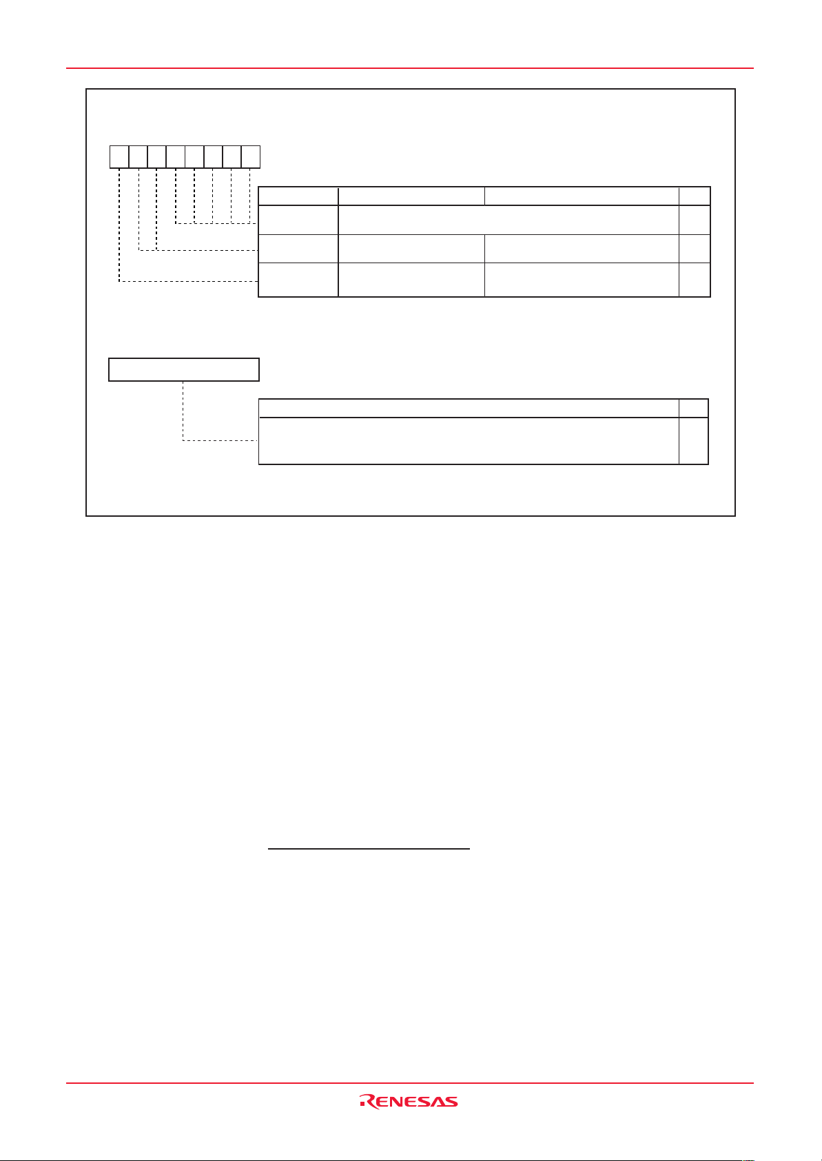
Under development
This document is under development and its contents are subject to change.
M16C/6N Group (M16C/6NL, M16C/6NN) 10. Watchdog Timer
Watchdog Timer Control Register
b7 b6 b5 b4 b3 b2 b1 b0
00
Symbol Address After Reset
WDC 000Fh 00XXXXXXb
Bit Name
-
(b4-b0)
-
(b6-b5)
WDC7
Watchdog Timer Start Register
b7 b0
NOTE
1. Write to the WDTS register after the watchdog timer interrupt request is generated.
Symbol Address After Reset
WDTS 000Eh Indeterminate
The watchdog timer is initialized and starts counting after a write instruction to
this register. The watchdog timer value is always initialized to "7FFFh" regardless
of whatever value is written.
High-order Bit of Watchdog Timer
Reserved Bit Set to "0"
Prescaler Select Bit
(1)
Function
0 : Divided by 16
1 : Divided by 128
FunctionBit Symbol
RW
RO
RW
RW
RW
WO
Figure 10.2 WDC Register and WDTS Register
10.1 Count Source Protective Mode
In this mode, a on-chip oscillator clock is used for the watchdog timer count source. The watchdog timer
can be kept being clocked even when CPU clock stops as a result of runaway.
Before this mode can be used, the following register settings are required:
(1) Set the PRC1 bit in the PRCR register to “1” (enable writes to the PM1 and PM2 registers).
(2) Set the PM12 bit in the PM1 register to “1” (reset when the watchdog timer underflows).
(3) Set the PM22 bit in the PM2 register to “1” (on-chip oscillator clock used for the watchdog timer count source).
(4) Set the PRC1 bit in the PRCR register to “0” (disable writes to the PM1 and PM2 registers).
(5) Write to the WDTS register (watchdog timer starts counting).
Setting the PM22 bit to “1” results in the following conditions:
• The on-chip oscillator starts oscillating, and the on-chip oscillator clock becomes the watchdog timer
count source.
Watchdog timer period =
Watchdog timer count (32768)
on-chip oscillator clock
• The CM10 bit in the CM1 register is disabled against write. (Writing a “1” has no effect, nor is stop mode entered.)
• The watchdog timer does not stop when in wait mode or hold state.
Rev.1.02 Jul 01, 2005 page 77 of 314
REJ09B0126-0102
Page 94

Under development
This document is under development and its contents are subject to change.
M16C/6N Group (M16C/6NL, M16C/6NN) 11. DMAC
11. DMAC
The DMAC (Direct Memory Access Controller) allows data to be transferred without the CPU intervention.
Two DMAC channels are included. Each time a DMA request occurs, the DMAC transfers one (8- or 16-bit)
data from the source address to the destination address. The DMAC uses the same data bus as used by the
CPU. Because the DMAC has higher priority of bus control than the CPU and because it makes use of a
cycle steal method, it can transfer one word (16 bits) or one byte (8 bits) of data within a very short time after
a DMA request is generated. Figure 11.1 shows the block diagram of the DMAC. Table 11.1 shows the
DMAC specifications. Figures 11.2 to 11.4 show the DMAC related-registers.
Address bus
DMA0 source pointer SAR0
DMA0 destination pointer DAR0
DMA0 transfer counter reload register TCR0
DMA0 transfer counter TCR0
DMA1 transfer counter reload register TCR1
DMA1 transfer counter TCR1
Data bus low-order bits
Data bus high-order bits
NOTE:
1.Pointer is incremented by a DMA request.
Figure 11.1 DMAC Block Diagram
DMA0 forward address pointer
DMA1 source pointer SAR1
DMA1 destination pointer DAR1
DMA1 forward address pointer
DMA latch high-order bits
DMA latch low-order bits
(1)
(1)
A DMA request is generated by a write to the DSR bit in the DMiSL register (i = 0, 1), as well as by an
interrupt request which is generated by any function specified by the DMS and DSEL3 to DSEL0 bits in the
DMiSL register. However, unlike in the case of interrupt requests, DMA requests are not affected by the I flag
and the interrupt control register, so that even when interrupt requests are disabled and no interrupt request
can be accepted, DMA requests are always accepted. Furthermore, because the DMAC does not affect
interrupts, the IR bit in the interrupt control register does not change state due to a DMA transfer.
A data transfer is initiated each time a DMA request is generated when the DMAE bit in the DMiCON register
= 1 (DMA enabled). However, if the cycle in which a DMA request is generated is faster than the DMA
transfer cycle, the number of transfer requests generated and the number of times data is transferred may
not match. For details, refer to 11.4 DMA Request.
Rev.1.02 Jul 01, 2005 page 78 of 314
REJ09B0126-0102
Page 95

Under development
This document is under development and its contents are subject to change.
M16C/6N Group (M16C/6NL, M16C/6NN) 11. DMAC
Table 11.1 DMAC Specifications
Item Specification
No. of Channels 2 (cycle steal method)
Transfer Memory Space • From any address in the 1-Mbyte space to a fixed address
• From a fixed address to any address in the 1-Mbyte space
• From a fixed address to a fixed address
Maximum No. of Bytes Transferred 128 Kbytes (with 16-bit transfer) or 64 Kbytes (with 8-bit transfer)
DMA Request Factors
(1) (2)
Falling edge of INT0 or INT1
________ ________
________ ________
Both edge of INT0 or INT1
Timer A0 to timer A4 interrupt requests
Timer B0 to timer B5 interrupt requests
UART0 transfer, UART0 reception interrupt requests
UART1 transfer, UART1 reception interrupt requests
UART2 transfer, UART2 reception interrupt requests
SI/O3, SI/O4 interrupt requests
A/D conversion interrupt requests
Software triggers
Channel Priority DMA0 > DMA1 (DMA0 takes precedence)
Transfer Unit 8 bits or 16 bits
Transfer Address Direction forward or fixed (The source and destination addresses cannot both be
in the forward direction.)
Transfer Mode Single Transfer Transfer is completed when the DMAi transfer counter underflows
after reaching the terminal count.
Repeat Transfer When the DMAi transfer counter underflows, it is reloaded with the value
of the DMAi transfer counter reload register and a DMA transfer is
continued with it.
DMA Interrupt Request When the DMAi transfer counter underflowed
Generation Timing
DMA Start Up Data transfer is initiated each time a DMA request is generated when the
The DMAE bit in the DMAiCON register = 1 (enabled).
DMA Shutdown Single Transfer • When the DMAE bit is set to “0” (disabled)
• After the DMAi transfer counter underflows
Repeat Transfer When the DMAE bit is set to “0” (disabled)
Reload Timing for Forward When a data transfer is started after setting the DMAE bit to “1” (enabled),
Address Pointer and Transfer the forward address pointer is reloaded with the value of the SARi or the
Counter DARi pointer whichever is specified to be in the forward direction and the
DMAi transfer counter is reloaded with the value of the DMAi transfer
counter reload register.
i = 0, 1
NOTES:
1. DMA transfer is not effective to any interrupt. DMA transfer is affected neither by the I flag nor by the
interrupt control register.
2. The selectable causes of DMA requests differ with each channel.
3. Make sure that no DMAC-related registers (addresses 0020h to 003Fh) are accessed by the DMAC.
Rev.1.02 Jul 01, 2005 page 79 of 314
REJ09B0126-0102
Page 96

Under development
This document is under development and its contents are subject to change.
M16C/6N Group (M16C/6NL, M16C/6NN) 11. DMAC
DMA0 Request Cause Select Register
b7 b6 b5 b4 b3 b2 b1 b0
Symbol Address After Reset
DM0SL 03B8h 00h
Bit Name
FunctionBit Symbol
DSEL0
DSEL1
DSEL2
DMA Request Cause
Select Bit
See NOTE 1
DSEL3
-
(b5-b4)
DMS
Nothing is assigned. When write, set to "0".
When read, their contents are "0".
DMA Request Cause
Expansion Select Bit
0 : Basic cause of request
1 : Extended cause of request
A DMA request is generated by setting
this bit to "1" when the DMS bit is "0"
(basic cause) and the DSEL3 to DSEL0
bits are "0001b" (software trigger).
DSR
Software DMA
Request Bit
The value of this bit when read is "0".
NOTE:
1. The causes of DMA0 requests can be selected by a combination of the DMS bit and the DSEL3 to DSEL0 bits
in the manner described below.
DSEL3 to DSEL0 Bits
0000b
0001b
0010b
0011b
0100b
0101b
0110b
0111b
1000b
1001b
1010b
1011b
1100b
1101b
1110b
1111b
DMS = 0 (basic cause of request) DMS = 1 (extended cause of request)
Falling edge of INT0 pin
Software trigger —
Timer A0 —
Timer A1 —
Timer A2 —
Timer A3
Timer A4
Timer B0
Timer B1
Timer B2 Timer B5
UART0 transmit
UART0 receive —
UART2 transmit —
UART2 receive —
A/D conversion —
UART1 transmit —
—
—
Two edges of INT0 pin
Timer B3
Timer B4
—
RW
RW
RW
RW
RW
-
RW
RW
Figure 11.2 DM0SL Register
Rev.1.02 Jul 01, 2005 page 80 of 314
REJ09B0126-0102
Page 97

Under development
This document is under development and its contents are subject to change.
M16C/6N Group (M16C/6NL, M16C/6NN) 11. DMAC
DMA1 Request Cause Select Register
b7 b6 b5 b4 b3 b2 b1 b0
Symbol Address After Reset
DM1SL 03BAh 00h
Bit Name
FunctionBit Symbol
DSEL0
DSEL1
DSEL2
DMA Request Cause
Select Bit
See NOTE 1
DSEL3
-
(b5-b4)
DMS
Nothing is assigned. When write, set to "0".
When read, their contents are "0".
DMA Request Cause
Expansion Select Bit
0 : Basic cause of request
1 : Extended cause of request
A DMA request is generated by setting
DSR
Software DMA
Request Bit
this bit to "1" when the DMS bit is "0"
(basic cause) and the DSEL3 to DSEL0
bits are "0001b" (software trigger).
The value of this bit when read is "0".
NOTE:
1. The causes of DMA1 requests can be selected by a combination of the DMS bit and the DSEL3 to DSEL0 bits
in the manner described below.
DSEL3 to DSEL0 Bits
0000b
0001b
0010b
0011b
0100b
0101b
0110b
0111b
1000b
1001b
1010b
1011b
1100b
1101b
1110b
1111b
DMS = 0 (basic cause of request) DMS = 1 (extended cause of request)
Falling edge of INT1 pin
Software trigger —
Timer A0 —
Timer A1 —
Timer A2 —
Timer A3
Timer A4
Timer B0
Timer B1
Timer B2
UART0 transmit
UART0 receive/ACK0 —
UART2 transmit —
UART2 receive/ACK2 —
A/D conversion —
UART1 transmit/ACK1 —
—
SI/O3
SI/O4
Two edges of INT1 pin
—
—
—
RW
RW
RW
RW
RW
-
RW
RW
DMAi Control Register (i = 0, 1)
b7 b6 b5 b4 b3 b2 b1 b0
NOTES:
1. The DMAS bit can be set to "0" by writing "0" in a program. (This bit remains unchanged even if "1" is written.)
2. At least one of the DAD and DSD bits must be "0" (address direction fixed).
Figure 11.3 DM1SL Register, DM0CON and DM1CON Registers
Symbol Address After Reset
DM0CON 002Ch 00000X00b
DM1CON 003Ch 00000X00b
Bit Name
DMBIT
DMASL
DMAS
DMAE
DSD
DAD
-
(b7-b6)
Transfer Unit Bit
Select Bit
Repeat Transfer Mode
Select Bit
DMA Request Bit
DMA Enable Bit
Source Address Direction
Select Bit
(2)
Destination Address
Direction Select Bit
(2)
Nothing is assigned. When write, set to "0".
When read, their contents are "0".
0 : 16 bits
1 : 8 bits
0 : Single transfer
1 : Repeat transfer
0 : DMA not requested
1 : DMA requested
0 : Disabled
1 : Enabled
0 : Fixed
1 : Forward
0 : Fixed
1 : Forward
FunctionBit Symbol
RW
RW
RW
(1)
RW
RW
RW
RW
-
Rev.1.02 Jul 01, 2005 page 81 of 314
REJ09B0126-0102
Page 98

Under development
This document is under development and its contents are subject to change.
M16C/6N Group (M16C/6NL, M16C/6NN) 11. DMAC
DMAi Source Pointer (i = 0, 1)
(b23)
b7
(b19) (b16)
(b15) (b8)
b0 b7 b0b3
Set the source address of transfer
(1)
b7 b0
Function
Symbol After Reset
SAR0
SAR1
Address
0022h to 0020h
0032h to 0030h
Indeterminate
Indeterminate
Setting Range
00000h to FFFFFh
Nothing is assigned. When write, set to "0".
When read, their contents are "0".
NOTE:
1. If the DSD bit in the DMiCON register is "0" (fixed), this register can only be written to when the DMAE bit in the
DMiCON register is "0" (DMA disabled).
If the DSD bit is "1" (forward direction), this register can be written to at any time.
If the DSD bit is "1" and the DMAE bit is "1" (DMA enabled), the DMAi forward address pointer can be read from
this register. Otherwise, the value written to it can be read.
DMAi Destination Pointer (i = 0, 1)
(b23)
b7
(b19) (b16)
(b15) (b8)
b0 b7 b0b3
Set the destination address of transfer
(1)
b7 b0
Function
Symbol After Reset
DAR0
DAR1
Address
0026h to 0024h
0036h to 0034h
Indeterminate
Indeterminate
Setting Range
00000h to FFFFFh
RW
RW
-
RW
RW
Nothing is assigned. When write, set to "0".
When read, their contents are "0".
-
NOTE:
1. If the DAD bit in the DMiCON register is "0" (fixed), this register can only be written to when the DMAE bit in the
DMiCON register is "0" (DMA disabled).
If the DAD bit is "1" (forward direction), this register can be written to at any time.
If the DAD bit is "1" and the DMAE bit is "1" (DMA enabled), the DMAi forward address pointer can be read from
this register. Otherwise, the value written to it can be read.
DMAi Transfer Counter (i = 0, 1)
(b15)
Figure 11.4 SAR0 and SAR1 Registers, DAR0 and DAR1 Registers, TCR0 and TCR1 Registers
(b8)
b0 b7
b0b7
Symbol After Reset
TCR0
TCR1
Function
Set the transfer count minus 1.
The written value is stored in the DMAi transfer counter
reload register, and when the DMAE bit in the DMiCON
register is set to "1" (DMA enabled) or the DMAi transfer
counter underflows when the DMASL bit in the DMiCON
register is "1" (repeat transfer), the value of the DMAi
transfer counter reload register is transferred to the DMAi
transfer counter.
When read, the DMAi transfer counter is read.
Address
0029h, 0028h
0039h, 0038h
Setting Range
0000h to FFFFh
Indeterminate
Indeterminate
RW
RW
Rev.1.02 Jul 01, 2005 page 82 of 314
REJ09B0126-0102
Page 99

Under development
This document is under development and its contents are subject to change.
M16C/6N Group (M16C/6NL, M16C/6NN) 11. DMAC
11.1 Transfer Cycle
The transfer cycle consists of a memory or SFR read (source read) bus cycle and a write (destination write)
bus cycle. The number of read and write bus cycles is affected by the source and destination addresses of
transfer. The bus cycle itself is extended by a software wait.
11.1.1 Effect of Source and Destination Addresses
If the transfer unit and data bus both are 16 bits and the source address of transfer begins with an odd
address, the source read cycle consists of one more bus cycle than when the source address of transfer
begins with an even address.
Similarly, if the transfer unit and data bus both are 16 bits and the destination address of transfer begins
with an odd address, the destination write cycle consists of one more bus cycle than when the destination
address of transfer begins with an even address.
11.1.2 Effect of Software Wait
For memory or SFR accesses in which one or more software wait states are inserted, the number of bus
cycles required for that access increases by an amount equal to software wait states.
Figure 11.5 shows the example of the cycles for a source read. For convenience, the destination write cycle
is shown as one cycle and the source read cycles for the different conditions are shown. In reality, the
destination write cycle is subject to the same conditions as the source read cycle, with the transfer cycle
changing accordingly. When calculating transfer cycles, take into consideration each condition for the
source read and the destination write cycle, respectively. For example, when data is transferred in 16- bit unit
using an 8-bit bus ((2) on Figure 11.5), two source read bus cycles and two destination write bus cycles are
required.
Rev.1.02 Jul 01, 2005 page 83 of 314
REJ09B0126-0102
Page 100

Under development
This document is under development and its contents are subject to change.
M16C/6N Group (M16C/6NL, M16C/6NN) 11. DMAC
(1) When the transfer unit is 8 or 16 bits and the source of transfer is an even address
BCLK
Address
bus
CPU use
Destination
Dummy
cycle
CPU useSource
RD signal
WR signal
Data
bus
CPU use CPU use
Source
Destination
Dummy
cycle
(2) When the transfer unit is 16 bits and the source address of transfer is an odd address, or when the
transfer unit is 16 bits and an 8-bit bus is used
BCLK
Address
bus
CPU use
Source + 1
Destination
Dummy
cycle
CPU useSource
RD signal
WR signal
Data
bus
CPU use CPU use
Source
Source + 1
Destination
Dummy
cycle
(3) When the source read cycle under condition (1) has one wait state inserted
BCLK
Address
bus
CPU use
Source
Destination
Dummy
cycle
RD signal
WR signal
Data
bus
CPU use CPU use
Source
Destination
Dummy
cycle
(4) When the source read cycle under condition (2) has one wait state inserted
BCLK
Address
bus
RD signal
WR signal
Data
bus
CPU use
CPU use CPU use
Source
Source + 1
Source + 1
Destination
Destination
CPU use
Dummy
cycle
Dummy
cycle
CPU useSource
NOTE:
1. The same timing changes occur with the respective conditions at the destination as at the source.
Figure 11.5 Transfer Cycles for Source Read
Rev.1.02 Jul 01, 2005 page 84 of 314
REJ09B0126-0102
 Loading...