


REALTEK SINGLE CHIP
8-PORT 10/100 ETHERNET
SWITCH CONTROLLER
WITH EMBEDDED MEMORY
RTL8308B
1. Features ................................................................2
2. General Description ............................................3
3. Block Diagram .....................................................4
4. Pin Assignments...................................................5
5. Pin Description ....................................................6
5.1 RMII Interface ................................................6
5.2 Serial EEPROM 24LC02 Interface.................7
5.3 System Pins.....................................................7
5.4 Mode Pins (Reset-Read) .................................7
5.5 LED Pin ..........................................................8
5.6 Test Pin............................................................8
5.7 Power & Ground Pins .....................................8
6. Functional Description........................................9
6.1 Reset................................................................9
6.2 Network Interface ...........................................9
6.2.1 Medium Access Control ..........................9
6.2.2 Auto Negotiation....................................10
6.2.3 MII Interface..........................................10
6.2.4 RMII interface .......................................10
6.2.5 Illegal Frames ........................................11
6.3 EEPROM Interface .......................................11
6.4 Serial Management Interface MDC/MDIO ..12
6.5 Reversible PHYAD Order.............................13
6.6 Address Search and Learning .......................13
6.7 Address Hashing Mode.................................14
6.8 Address Direct Mapping Mode.....................14
6.9 Frame Filtering..............................................14
RTL8308B
6.10 Back off Algorithm .................................... 15
6.11 Inter-Frame Gap ......................................... 15
6.12 Buffer Management.................................... 15
6.13 Buffer Manager .......................................... 15
6.14 Data Reception ........................................... 16
6.15 Data Forwarding......................................... 16
6.16 Flow Control .............................................. 17
6.17 Cut Through ............................................... 17
6.18 Broadcast Storm Filtering Control ............. 17
6.19 Loop Detection........................................... 18
6.20 Head-Of-Line Blocking.............................. 18
6.21 24LC02 Interface........................................ 18
6.22 24LC02 Device Operation ......................... 19
6.23 Testing ........................................................ 21
6.23.1 External SRAM Test ........................... 21
6.23.2 Production Testing .............................. 21
6.23.3 Loopback............................................. 21
7. 24LC02 Serial EEPROM Format ................... 22
8. Electrical Characteristics................................. 23
8.1 Temperature Limit Ratings........................... 23
8.2 DC Characteristics........................................ 23
8.3 AC Characteristics........................................ 23
8.3.1 Reset and Clock Timing........................ 23
8.3.2 RMII Timing ......................................... 24
8.3.3 PHY Management Timing .................... 25
8.3.4 Serial EEPROM 24LC02 Timing ......... 26
9. Mechanical Information................................... 27
2002/01/23 Rev. 2.0
1

1. Features
Supports eight 10/100Mbps Ethernet ports with
RMII interface
Provides forwarding of non-blocking and
non-head-of-line-blocking
2M bit DRAM built in as a packet storage buffer
Page based buffer management to efficiently
utilize the internal packet buffer
Ultra low power consumption with less than
160mA at 3.3V operating voltage
Embedded 8K entry look-up table and 128 entry
CAM
Supports address hashing or direct mapping for
look-up table
RTL8308B
Broadcast storm control
Flow control fully supported:
Half-duplex: back pressure
Full-duplex: IEEE 802.3X
Auto-negotiated Full-duplex flow control by
writing the ability via MDIO to external PHY
Supports Store-and-forward and cut-through
operation
Provides an LED display to indicate network loop
existence
Reversible PHYAD order for diverse PHY usage
3.3V 24LC02 interface
128-entry CAM is used to eliminate the hash
collision issues
Supports full and half duplex operation
Link, speed and duplex status are auto-detected via
MDIO
Optional EEPROM 24LC02 for Loop detect
configuration
128-pin PQFP, 0.35 um, 3.3V CMOS technology
2002/01/23 Rev. 2.0
2
RTL8308B
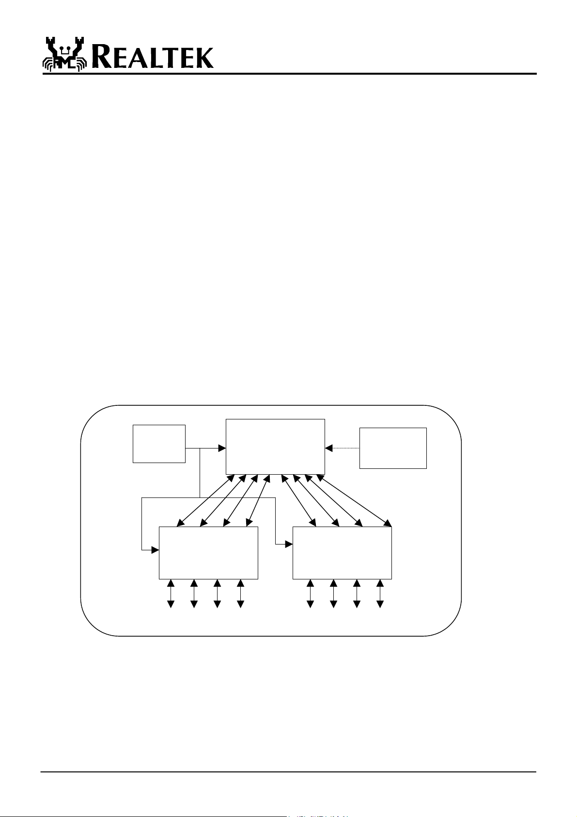
2. General Description
The RTL8308B is a 128-pin, low cost and ultra low power consumption 8-port 10/100M Ethernet switch controller.
It is integrated both with a 2M bit embedded DRAM, as a packet buffer, and an 8K entry address table. The
RTL8308B supports the reduced MII (RMII) interface. Only a single 50MHz oscillator is needed and the
EEPROM is optional, which can save BOM costs. In addition, the RTL8308B provides an LED display to indicate
a network loop existence.
The RTL8308B provides eight 10/100 Mbps RMII Ethernet ports. Each port can operate in 10 Mbps or 100 Mbps
data rate, and in full or half duplex mode. Speed, duplex, link status and flow control can be acquired by
periodically polling the status of the PHY devices via MDIO.
The address look-up table consists of an 8K entry hash table and a 128 entry CAM. The RTL8308B uses the
address hashing algorithm or direct mapping method to search destination MAC addresses from and record source
MAC addresses to the hash table. Data received from the MAC interface is stored in the external memory buffer.
The RTL8308B supports IEEE 802.3x full duplex flow control and half duplex back pressure control. The ability
of IEEE 802.3x flow control is auto-negotiated by writing the flow control ability via MDIO. The reversible
PHYAD order feature is provided to connect diverse external PHY devices for PCB layout.
The RTL8308B provides a loop detect LED for visual diagnostics when detecting the network loop. The Broadcast
storm filtering function is provided for unusual broadcast storm traffic.
The RTL8308B supports non-blocking 148800 packets/second wire speed forwarding rate and a special design to
resolve the head-of-line-blocking problem. The RTL8308B uses a 2-wire 24LC02 interface to access the external
serial EEPROM, which is not required. Only one 50MHz OSC is needed.
50MHz
OSC
Quad-PHY
Realtek
RTL8308B
Quad-PHY
10/100 Mbps x 8
EEPROM2
4LC02
2002/01/23 Rev. 2.0
Example of 8-port Switch System diagram
3
RTL8308B
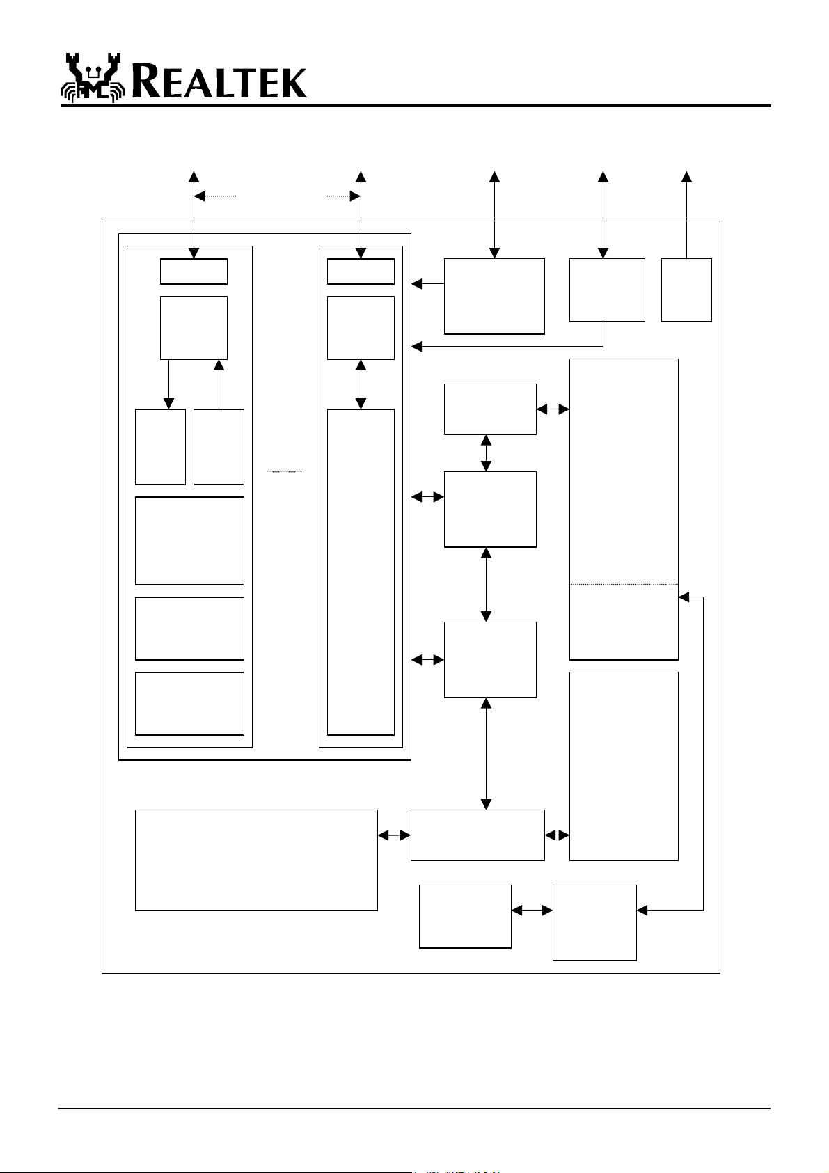
3. Block Diagram
8 Ports
RMII RMII PHY EEPROM LED
Management I/F I/F
10/100 10/100 I/F
MAC MAC
EDORAM Packet
I/F Buffer
RXFIFO TXFIFO Space
FIFOs,
QUEUE, DMA
Flow Engine
TX Start Addr. Control,
Queue
RX/TX Page
RX/TX F.P.P. F.P.P. Pointer
FIFOs FIFO Switching Space
Logic
Flow control
8K-entry
Address
Table
Address-Lookup
128-entry Address CAM Engine
F.P.P Buffer
FIFO Manager
2002/01/23 Rev. 2.0
4
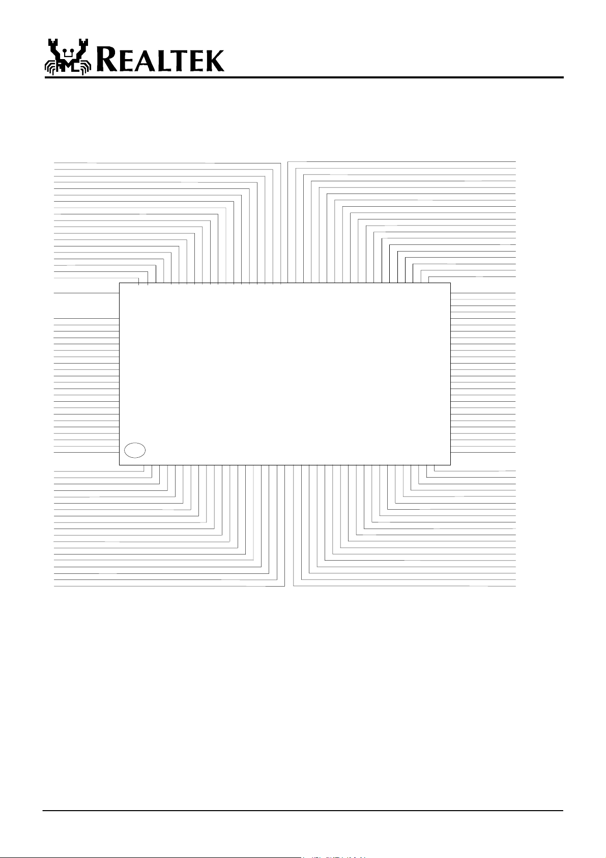
4. Pin Assignments
84 NC
85 VCC
86 TXE[G]
87 TXD0[G]
88 TXD1[G]
89 CRSDV[G]
90 RXD0[G]
91 RXD1[G]
92 TXE[H]
93 TXD0[H]
94 TXD1[H]
95 VCC
96 CRSDVH]
97 RXD0[H]
98 RXD1[H]
99 NC
100 NC
101 GND
102 NC
103 VCC
104 NC
105 GND
106 TEST
107 ENBKPRS
108 EnBrdCtrl
109 VCC
110 NC
111 GND
112 ENFCTRL
113 VCC
114 NC
115 GND
116 GND
117 ENCUTHR
118 NC
119 SYSCLK
120 NC
121 SCLK
122 SDA
123 NC
124 VCC
125 NC
126 GND
127 NC
128 VCC
RTL8308B
RTL8308B
83 GND
82 GND
81 RXD1[F]
80 RXD0[F]
79 CRSDV[F]
78 TXD1[F]
77 TXD0[F]
76 TXE[F]
75 GND
74 RXD1[E]
73 RXD0[E]
72 CRSDV[E]
71 GND
70 TXD1[E]
69 TXD0[E]
68 TXE[E]
67 NC
66 VCC
65 NC
64 GND
63 RXD1[D]
62 RXD0[D]
61 CRSDV[D]
60 TXD1[D]
59 TXD0[D]
58 TXE[D]
57 NC
56 NC
55 NC
54 LOOPLED#
53 RST#
52 VCC
51 VCC
50 NC
49 GND
48 GND
47 REFCLK
46 NC
45 NC
44 MDIO
43 MDC
42 NC
41 NC
40 VCC
39 VCC
1 NC
2 NC
3 NC
4 NC
5 NC
6 GND
7 TXE[A]
8 TXD0[A]
9 TXD1[A]
10 CRSDV[A]
11 RXD0[A]
12 RXD1[A]
13 TXE[B]
14 TXD0[B]
15 TXD1[B]
16 VCC
17 VCC
18 CRSDV[B]
19 RXD0[B]
38 NC
37 NC
36 GND
35 GND
34 GND
33 NC
32 NC
31 RXD1[C]
30 GND
29 RXD0[C]
28 CRSDV[C]
26 TXD0[C]
25 VCC
24 TXE[C]
27 TXD1[C]
23 GND
22 GND
21 GND
20 RXD1[B]
2002/01/23 Rev. 2.0
5

5. Pin Description
5.1 RMII Interface
Symbol Type Pin No Description
TXEN[A:H] O 7,13,24,58,
68,76,86,92
TXD[0:1][A],
TXD[0:1][B],
TXD[0:1][C],
TXD[0:1][D],
TXD[0:1][E],
TXD[0:1][F],
TXD[0:1][G],
TXD[0:1][H]
CRSDV[A:H] I 10,18,28,61,
RXD[0:1][A],
RXD[0:1][B],
RXD[0:1][C],
RXD[0:1][D],
RXD[0:1][E],
RXD[0:1][F],
RXD[0:1][G],
RXD[0:1][H]
REFCLK I 47
MDC O 43
O 8,9,14,15,26,
27,59,60,69,
70,77,78,87,88,
93,94
72,79,89,96
I 11,12,19,20,
29,31,62,63,
73,74,80,81,
90,91,97,98
Transmit Enable: The RTL8308B asserts high to indicate
that valid di-bit data for transmission is presented on
TXD[1:0], and transitions synchronously with respect to
REFCLK.. TXEN will be asserted synchronously with the first
nibble of the preamble and will remain asserted while all
di-bits that are to be transmitted are presented. TXEN will be
negated prior to the first REFCLK rising edge following the
final di-bit of a frame.
Transmit Data [1:0]: TXD[1:0] will transition synchronously
with respect to REFCLK. When TXEN is asserted, TXD[1:0]
is accepted for transmission by the PHY. TXD[1:0] will be
‘00’ to indicate idle when TXEN is deasserted.
CRSDV Signals: This signal will be asserted high by the
PHY when the medium is active. It is asserted asynchronously
on detection of carrier due to criteria defined in the IEEE
802.3 specifications. Loss of carrier will result in the
deassertion of this pin, synchronous to the cycle of the
reference clock, REFCLK.
Receive Data [1:0]: The RTL8308B captures the receive data
on the rising edge of REFCLK when CRSDV is asserted high.
When CRSDV is asserted high, RXD[1:0] will transition
synchronously to REFCLK. For each clock period in which
CRSDV is asserted, RXD[1:0] transfers two bits of recovered
data from the PHY. Values other than ‘00’ on RXD[1:0] while
RXDV as recovered from CRSDV is deasserted will be
ignored by the controller. Upon assertion of CRSDV, the PHY
will ensure that RXD[1:0] = ‘00’ until proper receive
decoding takes place.
RMII Reference Clock Input: A continuous clock which
provides the timing reference for CRS_DV, RXD[1:0],
TX_EN, and TXD[1:0]. It is a 50 MHz OSC, 3.3V, +/-50ppm,
0˚ C ~70˚ C, symmetry 45%~55%, Rise/Fall time 5ns, supply
40mA.
It is assumed that the PHY uses REFCLK as the network clock so no
buffering is required on the transmit data path.
Management Data Clock: A clock source common to all
ports, generated by the controller with a frequency of 312.5
kHz, it is used to synchronize the MII data stream (MDIO) for
transferring MII management data between the controller and
transceivers.
RTL8308B
This pin is Tri-state at reset.
2002/01/23 Rev. 2.0
6

RTL8308B
MDIO I/O 44
Management Data Input/Output: This pin is used during the
MII setup process. The whole setup sequence will set Register
4h, address 16-20 of the PHY to 05E1h, REGISTER 0h to
value 1200h. It also advertises 100/10 full duplex with pause
capability & enables auto-negotiation. Sending after reset
signal release about 1.6ms.
This pin is Tri-state at reset.
5.2 Serial EEPROM 24LC02 Interface
Symbol Type Pin No Description
SCLK O 121 Serial Clock: Internally pulled high, this pin is used to enable
data transfers from the EEPROM to the controller.
This output is used to clock the serial EEPROM inputs and
outputs. It operates at 1.6us or 625KHz.
SDA I/O 122 Serial Data Input/Output: Internally pulled high, this pin is
used to obtain configuration data from the external serial
EEPROM after reset. The data is synchronized by MDC.
5.3 System Pins
Symbol Type Pin No Description
RST# I 53 Reset: Active low to a known reset state. After power-on reset
(low to high), the configuration modes from Mode Pins are
determined. Then, the contents of the serial EEPROM is
auto-loaded into and the RTL8308B, which begins to access
the management data of PHY devices.
SYSCLK I 119 System clock input: The same 50 MHz clock as REFCLK is
used.
5.4 Mode Pins (Reset-Read)
Symbol Type Pin No Description
ENBrdCtrl I 108 Enable Broadcast Storm Control detection: Pulled low
internally by default, Broadcast Storm Control is disabled. When
pulled high upon reset, Broadcast Storm Control is enabled.
ENCUTHR I 117 Enable Cut-through: Pulled low internally by default,
cut-through is disabled. When pulled high upon reset,
Cut-through is enabled.
ENBKPRS I 107 Enable Half duplex back pressure function: Pulled low
internally by default, back pressure is enabled. When pulled
low upon reset, back pressure is disabled.
ENFCTRL I 112 Enable Full Duplex Flow Control: Pulled low internally by
default, Flow Control is enabled. The flow control ability will
write to management register 4 of PHY device one and only
one time after power-on reset, for advertising. When pulled
low upon reset, the flow control function will be disabled.
2002/01/23 Rev. 2.0
7

RTL8308B
5.5 LED Pin
Symbol Type Pin No Description
LOOPLED# O 54 Loop Detected LED: Low active. This pin, asserted low
indicates that a network loop is detected.
DTESTOUT O 56 DRAM Test Output: For internal test use.
5.6 Test Pin
Symbol Type Pin No Description
CTEST I 106 Test pin: For internal use. Must be tied to ground for normal
operation.
5.7 Power & Ground Pins
Symbol Type Pin No Description
GND P 6,21,22,23,30,
34,35,36,48,
49,64,71,75,82,
83,101,105,111,
115,116,126
VCC P 16,17,25,39,40,
51,52,66,85,95,
103,109,113,
124,128
Please specify Analog/Digital Power & GND.
2002/01/23 Rev. 2.0
8

RTL8308B
6. Functional Description
6.1 Reset
The minimum required reset duration is 1us. After power on reset, the RTL8308B will determine some features
from the ENFCTRL, ENBKPRS and ENBrdCtrl pins, auto-load the content of 24LC02 serial EEPROM, and write
abilities to connected PHY management registers via MDC/MDIO. It is recommended that the RTL8308B and
connected PHYs use the same reset signal source. The PHY reset must be completed before the RTL8308B.
6.2 Network Interface
The RTL8308B has 8 10/100 Mbps Ethernet ports (port 0 to port 7) with Reduced MII (R-MII) interfaces. It has 1
MII port in addition to the 4 R-MII ports for 10/100Mbps Ethernet transceivers. Note that an MII interface operates
at 25MHz in 100Mbps transmission and 2.5MHz for 10Mbps transmission. Reduced MII interfaces use the same
50MHz clock rate for both 10Mbps and 100Mbps operation. All MII interfaces support auto-negotiation for
transmission speeds, duplex modes and flow control options.
6.2.1 Medium Access Control
The RTL8308B implements the IEEE Std 802.3 binary exponential back-off algorithm and conforms to IEEE
802.3 specifications.
Data received from the PHY is interpreted and assembled into the external buffer memory by the RTL8308B flow
controller. Interpretation involves detection and removal of the preamble, extraction of the address and FCS
verification. Also included is a jabber-detection timer to detect frames of greater than maximum length being
received on the network. In 10Mbps mode, the raw data received from the PHY as input is converted to 8-bit width
before further processing. Similarly, in 100Mbps mode, the data received from the external PHY is converted to
8-bit data width in the shifter. The data is then synchronized to the internal clock of the RTL8308B. Once the
100Mbps data has been deserialized it is handled no differently than the 10Mbps data. By default, the RTL8308B
detects collision signals by itself, which makes normal and reverse MII connection easy. Because signals from the
PHY are not synchronized with internal clocks of the RTL8308B, the Rx FIFO adjusts timing differences between
external & internal clocks. Data transmission requires more processing and data handling than data reception. This
is due to the overhead of implementing collision detection and recovery logic. Data entering from the FIFO is
serialized for transmission at the transmit clock rate (this also requires the data to be synchronized to the transmit
clock rate from the internal clock). Because the transmit clock is asynchronous with the internal clock of the
RTL8308B, the Tx FIFO is needed for timing adjustment. The Tx FIFO will also transmit JAM pattern and
PAUSE frames to work with the flow control mechanism in the Flow Control Unit.
The Tx FIFO handles the output of data to the PHY devices, and several error states are handled. If a collision is
detected in half duplex mode, the state machine jams the output. If the collision was late (after the first 64-bytes
have been transmitted), the frame is lost. If it is an early collision, the controller backs off before retrying. While
operating in full duplex mode, both carrier-sense (CRS) mode and collision-sensing modes are disabled. Internally,
frame data only is removed from buffer memory once it has been successfully transmitted without collision (for the
half-duplex ports). Transmission recovery also is handled in this state machine. If a collision is detected, frame
recovery and retransmission are initiated.
2002/01/23 Rev. 2.0
9

RTL8308B
6.2.2 Auto Negotiation
Each individual port can operate at 10Mbps or 100Mbps in half or full duplex mode, and can indicate support of
IEEE 802.3x flow control. The operating modes for each port can be negotiated between the MAC and PHY
devices after power up if auto-negotiation is enabled for that port. Auto-negotiation may be enabled for each port
by setting the corresponding auto-negotiation parameter through a configuration pin, EEPROM or serial
configuration interface. This provides for unmanaged operation, when using PHY devices that support this
signaling scheme.
6.2.3 MII Interface
Through the MII interface, the 10/100Mbps ports support a number of options, such as full/half duplex and
10M/100M bit rate. The architecture for the 100Mbps interface is similar to that for 10Mbps. This permits the
interface to support both 10 and 100Mbps operation. When operated at 10Mbps, the ports support nibble mode at
2.5 MHz clock rate.
6.2.4 RMII interface
The RTL8308B provides a 10/100 Mbps low pin count RMII interface for use between PHY and RTL8308. The
MAC of each port of RTL8308B is connected to the PHY through the standard RMII interface. The RMII is
capable of supporting 10Mbps and 100Mbps data rates. A single clock reference, 50MHz, sourced from an external
clock input is used for receiving and transmitting.
It also provides independent 2 bit wide (di-bit) transmit and receive data paths. As the REFCLK is 10 times the
data rate in 10Mbps mode, each data di-bit must be output on TXD[1:0] and input on RXD[1:0] for ten consecutive
REFCLK cycles. The RTL8308B can regenerate the COL signal of the MII internally by ANDing TXEN and CRS
as recovered from CRSDV. Note that TXEN cannot be ANDed directly with CRSDV since CRSDV may toggle at
the end of the frame to provide separation of RXDV and CRS.
Prior to any data transaction, RTL8308B will output di-bits of ‘01’ as preamble signal. After the preamble, a ‘11’
signal is used to indicate the start of the frame. For reception, the received data (RXD) is sampled by the rising
edge of the REFCLK. Assertion of the CRSDV signal indicates that the receive channel is active. The di-bit
RXD[1:0] is nominally ‘00’ until the PHY detects a valid SFD and sends a ‘01’ preamble. Valid data will follow
SFD. For transmission, TXEN is asserted when the first preamble nibble is sent on the transmit data (TXD) lines.
The transmit data is clocked out by the rising edge of the reference clock.
RMII Specification Signals are listed below:
Signal Name Direction
(with respect
to the PHY)
REFCLK Input Input Synchronous clock reference for receive,
CRSDV Output Input Carrier Sense/Receive Data Valid
RXD[1:0] Output Input Receive Date
TXEN Input Output Transmit Enable
TXD[1:0] Input Output Transmit Data
Direction
(with respect
to the RTL8308)
Use
transmit and control interface.
2002/01/23 Rev. 2.0
10

RTL8308B
6.2.5 Illegal Frames
During the receiving process, the MAC will monitor the length of the received frame. Illegal frames such as a bad
CRC packet, runt packet (less than 64 bytes) or oversized packet (greater than 1536) will be discarded.
If the carrier sense (CRS) signal in the RMII interface is asserted and RXD[1:0] at the beginning of the packet is
‘10’, the port is considered to have a false carrier event. Normal carrier has a preamble value of ‘01’. The false
carrier event is recorded for the MIB counter.
The RTL8308B can handle frames up to 1536 bytes. All frames longer than 1536 byte will be discarded. If the port
continues to receive data after the 1536th byte, the port’s data will be filtered. If the port is in half duplex mode, the
port will no longer be able to transmit or receive data during the long packet reception.
6.3 EEPROM Interface
The serial EEPROM interface is designed to load information required by various optional functions. The interface
implements the SDA signal and it is directly compatible with the 93C46 device. The controller reads, in serial
format, in the first 272 bits (seventeen 16-bit words) out of the EEPROM and stores them in registers. Because the
information stored in EEPROM is static, this read occurs only on power-up. The serial EEPROM shifts out the
most significant bit of the word first.
2002/01/23 Rev. 2.0
11

RTL8308B
6.4 Serial Management Interface MDC/MDIO
The RTL8308B supports PHY management through the serial MDIO and MDC signal lines. After power on reset,
the RTL8308B writes abilities to the advertisement register 4 of the connected PHY and restarts the
auto-negotiation process through MDIO using PHY addresses incrementally from 01000b to 01111b. After
restarting auto-negotiation, the RTL8308B will continuously poll the link status and link partner's ability which
includes speed, duplex and flow control of the PHY devices via MDIO.
The MDIO operation for the RMII is the same as that for the MII. The device will send a ‘01’ to signal a write
operation. The 5 bit ID address of the PHY device and the 5 bit register address is next, and a ‘10’ turn-around
signal is then used to avoid contention during a read transaction. After the turn around, the 16 bits of data will be
written into the register. After the completion of the write transaction, the line will be put into a high impedance
state.
For a read operation, the RTL8308Bwill output a ‘10’ to indicate read operation after the start of frame indicator.
The 5-bit ID address of the PHY device and the 5-bit register address is next. Then, the RTL8308Bwill stop
driving the MDIO line, and wait for one bit time. During this time, the MDIO should be in a high impedance state.
The device will then synchronize with the next bit of ‘0’ driven by the PHY device, and continue to read the 16 bits
of data from the register. The detailed timing requirements on PHY management signals are described in the
timing part of Section 8.
The MDIO port can be disabled through the use of the port configuration register. This allows usage of a
100Base-TX transceiver without auto-negotiation capability or an RMII to RMII interconnect. In this mode of
operation, the PHY has no communication with the RTL8308. Therefore, the RTL8308Bwill assert the link status
as soon as initialization is completed and assumes the connected PHY is operating at the specified operating mode
and speed.
2002/01/23 Rev. 2.0
12

RTL8308B
The Management frame format is listed below:
READ
WRITE
Management frame fields
PRE ST OP PHYAD REGAD TA DATA IDLE
1…1 01 10 AAAAA RRRRR Z0 DDDDDDDDDDDDDDDD Z
1…1 01 01 AAAAA RRRRR 10 DDDDDDDDDDDDDDDD Z
6.5 Reversible PHYAD Order
In order to maintain maximum flexibility, the RTL8308B provides a reversible PHYAD order feature. This allows
reverse ordering of the PHY addresses, which allows connection of the RTL8308B to diverse external PHY
devices. The addresses of ports [A] to [H] correspond to PHYAD 01000b to 01111b, or to PHYAD 01111b to
01000b, depending on the value of PHYAD_RV in the EEPROM.
6.6 Address Search and Learning
The address look-up table consists of an 8K entry hash table and a 128 entry CAM. The RTL8308B uses the hashing
algorithm or direct mapping method to search destination MAC addresses from and record source MAC address to
the table. If a hashed or mapped location is not empty, the RTL8308B will compare the destination MAC address with
the contents of the CAM for address searching and store source MAC address to CAM for learning.
The aging time of the MAC address is 300 seconds. The address hashing or direct mapping algorithm can be
selected via the 24LC02. A port’s MAC address register is cleared on power-up, or hardware reset. If the SA aging
option is enabled, the dynamically learned SA will be cleared if it is not refreshed in less than programmed time.
The table lookup engine provides the switching information required for routing the data packets. The address look
up table is set up through auto address learning (dynamic) or manual entry (static). The static addresses are
assigned to the address table by the EEPROM or management device. All static address entries will not be aged or
updated by the RTL8308B.
After a frame is received by RTL8308B, the embedded source address (SA) and destination addresses (DA) are
retrieved. The source address retrieved from the received frame is automatically stored in a SA buffer. The
RTL8308B will then check for error and security violation, and perform a SA search. If there is no error or security
violation, the chip will store the source address in the address lookup table. If the SA has been previously stored in
another port’s SA table, the RTL8308B will delete the SA from the previously stored location.
The Individual MAC Address is a 48-bit unique MAC address to be programmed or learned. Bit 0 of a SA will be
masked, i.e. no multicast SA.
The RTL8308B provides an on-chip MACAddress-To-PortID/TrunkID table with up to 1K entries for packet
destination look-up operation.
2002/01/23 Rev. 2.0
13

RTL8308B
The RTL8308B address table contains both the static addresses input by the CPU or the EEPROM and
dynamically learned address. It learns the individual MAC addresses from 3 different sources.
1. Packet received with no errors from the local ports.
2. Packets forwarded from other devices through the ring to the device
3. The Table Convergence message received from the ring, which is not issued by the device itself.
If a received packet contains a source address that has already been learned in another port’s address table but not
aged out, it will perform the following operation based on the switch’s configuration.
If the security option is selected for the port, RTL8308B will consider this as a security violation. If port is a
nonprotected port, RTL8308B will delete the SA from the previous port’s address table and update it to the current
port’s address table. However, if the SA is an static address entry, the address will not be updated.
6.7 Address Hashing Mode
On reception of a packet, the RTL8308B first hashes the destination MAC address to get a location index to the
8K-entry hash table At the same time, it compares the destination MAC address with the contents of the 128 entry
CAM. If the hash indexed location is valid or the CAM comparison matches, this received packet will be
forwarded to the corresponding destination port. Otherwise, the RTL8308B broadcasts the packet. Next, the
RTL8308B hashes the source MAC address to get a location index to the hash table. If the hash indexed location is
occupied, i.e., a hash collision has occurred, the new source MAC address will be relocated into the 128 entry
CAM accordingly. Using this eliminates the hash collision problem.
6.8 Address Direct Mapping Mode
In this mode, the RTL8308B uses the last 13 bits of the MAC address to index to the 8K-entry look-up table.
6.9 Frame Filtering
The RTL8308B will make filtering and forwarding decisions for each packet received based on its packet routing
table, VLAN Mapping, port state, and the system configuration.
Received frames will be filtered under the following conditions:
1. The RTL8308B will check all received frames for errors such as symbol error, FCS error, short event, runt, long
event, etc. Frames with any kind of error will not be forwarded to their destination port.
2. Any frame heading to its own source port will be filtered.
3. Packets heading to a disabled receiving port will be filtered.
4. If the input buffer of the port is full, the incoming frame will be discarded. It is recommended to use flow control
to prevent any loss of data. If the flow control option is enabled, this event will not occur. The remote station
will transmit a frame when the input buffer becomes available.
5. If the packet has any security violation and security option is enabled at the receiving port
2002/01/23 Rev. 2.0
14

RTL8308B
If the Spanning Tree Protocol is enabled, the RTL8308B will forward the packet as follows:
1. If the port is in the Block-N-Listen state or the Learning state, forward the packet to the CPU when it is a BPDU
packet, discard the packet otherwise;
2. If the port is in the Forwarding State, forward the packet to the CPU when it is a BPDU packet.
6.10 Back off Algorithm
The RTL8308B implements the truncated exponential back off algorithm compliant to the IEEE 802.3 standard.
The collision counter will be restarted after 16 consecutive collisions.
6.11 Inter-Frame Gap
The Inter-Frame Gap is 9.6us for 10Mbps Ethernet and is 960ns for 100Mbps fast Ethernet.
6.12 Buffer Management
An embedded 2M bit (32K x 64 ) or 256K byte DRAM operating at the 50MHz clock rate is built-in as a packet
storage buffer. To efficiently utilize the packet buffer, the RTL8308B divides the 2Mbit (256Kbytes) DRAM into
1K pages of storage space, i.e., each page contains 256 bytes. For Ethernet packets, a maximum of seven pages can
be used and the minimum is one.
The embedded DRAM is divided into two parts. The first is the Packet Buffer Space, used for storing received
packet data. The second is Page Pointer Space for buffer management. The Packet Buffer Space consists of about
1k storage units in a page. Each page consists of 8-byte Header information, including next page pointer and
received byte count, and 248 bytes of data. The page pointers are contained in Page Pointer Space.
Packet Buffer Space
(about 1K pages)
Page Pointer Space
2M bit DRAM
6.13 Buffer Manager
The Buffer Manager of the RTL8308B contains a Free Page Pointer FIFO pool to store and provide available free
page pointers to all ports. After power up reset, the Buffer Manager will initiate the Descriptor Read command to
get some available free page pointers from Page Pointer Space. When the contents of the Free Page Pointer FIFO is
almost empty due to continuous data receptions, the Descriptor Read command will be reinitiated to get more
available free page pointers. However, when the FIFO contents are almost full due to continuous successful data
transmissions, the RTL8308B initiates the Descriptor Write command to write the additional available free page
pointers back to Page Pointers Space.
2002/01/23 Rev. 2.0
15

RTL8308B
6.14 Data Reception
Each port contains a Receive Data FIFO and a Receive Free Page Pointer FIFO. Initially the Free Page Pointer
FIFO is filled with free page pointers received from the Buffer Manager. On reception of a packet, the received
data flows into the Receive Data FIFO first and then is moved into the Packet Buffer by the Receive DMA Engine,
using the free page pointers in the Receive Free Page Pointer FIFO via the Get Free Page command. The
RTL8308B always attempts to fill the Receive Free Page Pointer FIFO with free page pointers.
6.15 Data Forwarding
Each port also contains a Transmit Data FIFO, a Transmit Free Page Pointer FIFO and a Transmit Start Address Queue.
After a packet is received, its source address (SA) and destination address (DA) are retrieved. The SA is used to
update the port’s address table and the DA is used to determine the packet’s destination port. Once a forwarding
condition is met (for store-and-forward mode, a packet is completely received) the receiving port will pass the
beginning page pointer using the Send TX Descriptor command to the transmit port and start the Transmit DMA.
The transmission port stores the beginning page pointer in the Transmit Start address Queue. The Transmit DMA
moves data from the Packet Buffer through the Transmit Data FIFO and to the RMII interface using the free page
pointer in the Transmit Free Page Pointer FIFO. Once the packet has been forwarded successfully, the RTL8308B
uses the Put Free Page command to put related free page pointers back to buffer manager's Free Page Pointer FIFO.
The Address Lookup Engine will attempt to match the destination address with the addresses stored in the address
table. If there is a match found, a link between the source port and the destination port is then established.
If the first bit of the destination address is 0, the frame is regarded as an unicast frame. The destination address is
passed to the Address Lookup Engine; which returns a matched destination port number to identify which port
should the frame be forwarded to. If the destination port is within the same VLAN of the receiving port, the frame
will be forwarded.
If the destination port does not belong to the VLANs specified at the receiving ports, the frame will be discarded.
The event will be recorded as a VLAN boundary violation.
There are two ways that RTL8308B handles packet with unknown destination. The forwarding decision is
controlled by the Flood Control option (System Configuration register 00). If Flood Control is disabled, the packet
will be forwarded to all ports (except the receiving port) within the same VLANs of the receiving port. If the
FloodControl option is enabled, the RTL8308B will forward the packet only to the uplink port specified at the
receiving port.
RTL8308B defines a port as either a single port or a trunk.
If the port monitoring function is enabled, the packet forwarding decision is also subject to the port monitoring
configurations.
If the first bit of the destination address is a 1, the frame will be handled as a multicast or broadcast frame. The
RTL8308B does not differentiate multicast packet from broadcast packet except the reserved bridge management
group address, as specified in table 3.5 of IEEE 802.1d standard. The destination ports of the broadcast frame is all
ports within the same VLAN except the source port itself.
If Multicast/Broadcast packet trapping (MCtrap) is enabled, the multicast/broadcast packets will be forwarded to
the CPU only.
2002/01/23 Rev. 2.0
16

RTL8308B
6.16 Flow Control
The RTL8308B supports IEEE 802.3x full duplex flow control and half duplex back pressure congestion control.
The IEEE 802.3x flow control ability is auto-negotiated between a remote device and the RTL8308B by writing
the flow control ability via MDIO to the external, connected PHY. The RTL8308B adopts a special half duplex
back pressure design, forwarding one packet successfully after 28 force collisions to prevent the connected repeater
from being partitioned due to excessive collisions. The full duplex flow control ability can be enabled or disabled
via the ENFCTRL pin, and the half duplex back pressure function can be enabled or disabled via the ENBKPRS
pin, both during hardware reset.
If ENFCTRL is set and the 802.3x pause ability from the auto-negotiation result is enabled, the full duplex 802.3x
flow control function is enabled. Otherwise, the full duplex 802.3x flow control function is disabled. When 802.3x
flow control is enabled, the RTL8308B will only recognize the 802.3x flow control PAUSE ON/OFF frames with
DA="0180C2000001", type="8808", OP-code="01", PAUSE Time = maximum or zero, and with good CRC.
If a PAUSE frame is received from any PAUSE flow control enabled port with DA=0180C2000001, the
corresponding port of the RTL8308B will stop its packet transmission until a PAUSE timer timeout or another
PAUSE frame with zero PAUSE time is received. No 802.3x PAUSE frames received from any port will be
forwarded by the RTL8308B.
6.17 Cut Through
The RTL8308B can operate in cut-through or store-and-forward mode. When in cut through mode (by pulling the
ENCUTHR pin high), if receiving packet length is greater than 512 bytes, the RTL8308B starts to forward it after
512 bytes are received. If less than 512 bytes, the RTL8308B operates as same as store-and-forward mode.
6.18 Broadcast Storm Filtering Control
The RTL8308B can enable broadcast storm filtering control by pulling high EnBrdCtrl (pin108). This allows
limitation of the number of broadcast packets into the switch, and can be implemented on a per port basis. The
threshold of number of broadcast packets is set to 64. When enabled, each port will drop broadcast packets
(Destination MAC ID is ff ff ff ff ff ff) after receiving 64 continuous broadcast packets. The counter will be reset to
0 every 800ms or when receiving any non-broadcast packets (Destination MAC ID is not ff ff ff ff ff ff).
When disabled, or the number of non-unicast packets received at the port is not over the programmed threshold, the
RTL8308B will forward the packet to all the ports (except the receiving port) within the VLANs specified at the
receiving port. If the CPU port is within the specified VLAN, the packet will also be forwarded to the CPU.
If Broadcast-Storm-drop (BConly_SC) is enabled, the RTL8308B will only drop broadcast packets but not the
multicast packets.
2002/01/23 Rev. 2.0
17

RTL8308B
6.19 Loop Detection
When the loop detection function is enabled, by setting Enloop in EEPROM, the RTL8308B periodically sends out
a broadcast 64-byte packet every 3~5 minutes and automatically detects the existence of a network loop (or bridge
loop). The loop LED asserted low indicates that a loop exits. The LED will go out by unplugging both of the
RTL8308B ports of the loop. The Loop frame length is 64 bytes and its format is below.
FFFFF80F SID 0040 0000000…0000 CRC
In order to achieve loop detection, each switch device needs a different SID for detection. In addition, a different
EtherID is needed for each device when the loop detection function is enabled. If no EEPROM is used, the
RTL8308B uses a default SID (0180c2000001) and FCS.
6.20 Head-Of-Line Blocking
The RTL8308B incorporate a simple mechanism to prevent Head-Of-Line blocking problems when flow control is
disabled. When the flow control function is disabled, the RTL8308B will first check the destination address of the
incoming packet. If the destined port is congested, then the RTL8308B will discard this packet to avoid blocking
the next packet which is going to a non-congested port.
6.21 24LC02 Interface
The 24LC02 interface is a 2-wire serial EEPROM interface providing 2K bits of storage space. After a power on
reset, the RTL8308B uses Random Read and Sequential Read commands to auto-load configuration settings,
switch Ethernet ID, etc. After it is auto-loaded, the 24LC02 interface pins SCL and SDA are tri-stated for other
devices (e.g. PC parallel port or 8051 controller) to program the 24LC02 contents.
If a 24LC02 is not used, byte 0 of the 24LC02 would be read as FF. When byte 0 is not FF, the RTL8308B will
directly use the default value. The default values of byte 0 and byte 1 are 00. When the 24LC02 is not used, the
RTL8308B will also use default SID, FCS of Pause-On and Pause-off.
RTL8308B
SCLK
SDA
Programming
Device
24LC02
SCLK
SDA
2002/01/23 Rev. 2.0
18

RTL8308B
6.22 24LC02 Device Operation
Clock and Data transitions: The SDA pin is normally pulled high by an external resister. Data on the SDA pin may
change only during SCL low time periods. Data changes during SCL high periods will indicate a start or stop
condition as defined below.
Start condition: A high-to-low transition of SDA with SCL high is a start condition which must
precede any other command.
Stop condition: A low-to-high transition of SDA with SCL high is a stop condition.
Acknowledge: All addresses and data are transmitted serially to and from the EEPROM in 8-bit
words. The 24LC02 sends a zero to acknowledge that it has received each word. This
happens during the ninth clock cycle.
Random Read: A random read requires a "dummy" byte write sequence to load in the data word address.
Sequential Read: For the RTL8308, the sequential reads are initiated by a random address read. After
the 24LC02 receives a data word, it responds with an acknowledgement. As long as
the 24LC02 receives an acknowledgement, it will continue to increment the data word
address and serially clock out sequential data words.
*Start and Stop Definition
SDA
SCL
START STOP
*Output Acknowledge
SCL 1 8 9
DATA IN
DATA OUT
START ACKNOWLEDGE
2002/01/23 Rev. 2.0
19

*Random Read
START
WRITE
START
READ
DEVICE WORD DEVICE
ADDRESS ADDRESS n ADDRESS
SDA
DATA n
R/w
ACK
ACK
ACK
DUMMY WRITE
*Sequential Read
READ
ACK
ACK
RTL8308B
STOP
NO ACK
STOP
DEVICE
ADDRESS
SDA
DATA n DATA n+1 DATA n+x
ACK
R/W
ACK
ACK
NO ACK
2002/01/23 Rev. 2.0
20

RTL8308B
6.23 Testing
There are several testing and diagnostic options for the RTL8308B. This section will describe the External SRAM
Test, Production Testing and the External Loopback Test.
6.23.1 External SRAM Test
After RESET signal goes high, the RTL8308B will perform external memory self-test. It performs a worse case
test by changing Address & Data bus bits as much as possible between each access. The whole test takes about
14ms. The corresponding memory error indication bit accessible via serial LED interface will be turn on if any data
read is different from written.
6.23.2 Production Testing
The RTL8308B supports a simple but effective testing function for final production test in the process of switch
manufacturing. If board diagnostic function is enabled, the switch may act as a packet generator to be part of the
production test fixture to test finished switch system on production line. In this mode, the switch generates 16
broadcast packets on each port, from port 0 to port 4/7 sequentially. All other ports except the transmitting port
should received 16 valid packets. If any port failed to receive packets as expected, the switch will turn on the
corresponding RX ERR LED. Otherwise, RXOK LEDs will be lit. During the process of testing, the switch turns
on TXON LED of the transmitting port and RXON LED of all other ports. When the process completed
successfully, the switch will turn on the TESTOK LED. The switch will re-start testing cycle when a trigger signal
applied to the CFGIN pin or when a test cycle timer of 26 seconds expired. Note that all links must operate in full
duplex mode and transmit/receive at 100Mbps. Note that this feature is supported only when the switch in test
fixture and the switch in production are both designed based on the RTL8308B controllers.
6.23.3 Loopback
This feature is designed to simplify field support task for system manufacturers and distributors. In this mode, the
switch should have switch ports connected in pairs using cross-over CAT-5 cables. When external loop-back test is
enabled, the switch sends 16 packets on all active (connected) ports simultaneously. And each active port should
receive exactly 16 valid packets. . If any port failed to receive packets as expected, the switch will turn on the
corresponding RX ERR LED. Otherwise, RXOK LEDs will be lit. During the process of testing, the switch turns
on TXON LEDs and RXON LEDs of all active ports. When the process completed successfully, the switch will
turn on the TESTOK LED. The switch will re-start testing cycle when a trigger signal applied to the CFG_IN pin
or when a test cycle timer of 26 seconds expired. Note that all links must operate in full duplex mode and
transmit/receive at 100 Mbps.
2002/01/23 Rev. 2.0
21

RTL8308B
7. 24LC02 Serial EEPROM Format
The contents of the 24LC02 serial EEPROM are listed below. The contents include configuration, Switch Ethernet
ID, CRCs for flow control and loop detection.
Bit
Byte
0 EnLoop 0 0 0 AcceptErr 0 0 0
1 0 HashMode 0 0 0 0 0 PHYAD_RV
2-7 Ethernet ID (Physical Address) PAR47~0
8-11 Pause ON CRC 31~0
12-15 Pause OFF CRC 31~0
16-19 Loop Detection CRC 31~0
AcceptErr: When 0, CRC error packet will be discarded for normal use.
When 1, CRC Error packet can be accepted and forwarded for test.
EnLoop: When 0, the Loop detection function is disabled.
When 1, the Loop detection function is enabled.
PHYAD_RV: When 0, port[A]~[H] uses PHYAD = 01000b ~ 01111b to access external PHY status.
When 1, port[H]~[A] uses PHYAD = 01000b ~ 01111b.
HashMode: When 1, address hashing algorithm used for search and learning.
When 0, address direct mapping algorithm used.
If no 24LC02 is used, the default values of byte 0 and byte 1 are 00, and the default SID is 0180c2000001.
7 6 5 4 3 2 1 0
2002/01/23 Rev. 2.0
22

RTL8308B
8. Electrical Characteristics
8.1 Temperature Limit Ratings
Parameter Minimum Maximum Units
Storage temperature -55 +125 ˚C
Operating temperature 0 70 ˚C
8.2 DC Characteristics
Supply voltage Vcc = 3.3V ± 5%
Symbol Parameter Conditions Min. Ty pi cal Max. Units
VOH Minimum High Level Output
Voltage
VOL Maximum Low Level Output
Voltage
VIH Minimum High Level Input
Voltage
VIL Maximum Low Level Input
Voltage
IIN Input Current V
IOZ Tri-State Output Leakage Current V
ICC Average Operating Supply Current I
I
OH= -8mA
I
OL= 8mA
IN=VCC or GND
OUT=VCC or
GND
OUT=
0.9 * Vcc Vcc V
0.1 * Vcc V
0.5 * Vcc Vcc+0.5 V
-0.5 0.3 * Vcc V
0mA, 145 160 mA
-1.0 1.0 µA
-10 10 µA
8.3 AC Characteristics
8.3.1 Reset and Clock Timing
Symbol Description Min. Ty pi c al Max. Units
clock (SYSCK)
f
t1 SYSCLK clock period 15 20 25 ns
t2 RST# low pulse duration 1000 - - ns
VDD
SYSCLK
RST#
SYSCLK clock frequency 40 50 66 MHZ
t1
t2
Reset and Clock Timing
2002/01/23 Rev. 2.0
23

RTL8308B
8.3.2 RMII Timing
Symbol Description Min. Ty pi cal Max. Units
t1 REFCLK clock period - 20 - ns
t2 REFCLK high level width - 10 - ns
t3 REFCLK low level width - 10 - ns
t4 TXE,TXD to REFCLK rising setup time 4 - - ns
t5 TXE,TXD to REFCLK rising hold time 2 - - ns
t6 CSRDV,RXD to REFCLK rising setup
time
t7 CRSDV,RXD to REFCLK rising hold time 2 - - ns
t2
REFCLK
TXE
t4
t5
4 - - ns
t1
t3
TXD[1:0]
TX DATA
RMII Transmit Timing
t1
t2
REFCLK
CRSDV
t6
RXD[1:0]
RX DATA
RMII Receive Timing
t3
t7
2002/01/23 Rev. 2.0
24

8.3.3 PHY Management Timing
Symbol Description
t1 MDC clock period - SYSCK *
t2 MDC high level width - SYSCK *
t3 MDC low level width - SYSCK *
t4 MDIO to MDC rising setup time (Write
Bits)
t5 MDIO to MDC rising hold time (Write
Bits)
t6 MDC to MDIO delay (Read Bits) - - 20 ns
t7 MDC/MDIO actives from RST# deasserted - 94.377 - ms
t2 t3
Min.
10 - - ns
10 - - ns
t1
Typica l
32
16
16
Max.
- ns
- ns
- ns
RTL8308B
Units
MDC
MDIO
MDC
MDIO
t4
t5
data
MDIO Write Timing
t1
t2
t3
t6
MDIO Read Timing
data
2002/01/23 Rev. 2.0
25

RTL8308B
8.3.4 Serial EEPROM 24LC02 Timing
Symbol Description Min. Ty pi cal Max. Units
clock (EESCK)
f
t1 Clock pulse period 23 - - us
t2 Delay time, from SCLK rising to SDA falling 5 - - us
t3 Delay time, from SDA falling to SCLK falling 5 - - us
t4 Delay time, from SCLK falling to SDA changing 0 - - us
t5 Delay time, from SDA valid output to SCLK rising 0 - - us
t6 Stop Set-up time 5 - - us
t7 Time the bus must be free before a new transmission starts 5 - - us
t8 Delay time, from SCLK falling to SDA valid 0 - - us
t9 Delay time, from SCLK falling to SDA changing 0 - - us
t10 Delay time, from SDA valid input to SCLK rising 10 - - us
Clock frequency, SCLK - - 66 kHZ
t1
t2
SCLK
t2
t3
t4 t5
t6 t7
SDA
(output)
SDA
(input)
RST#
MDC
MDIO
VALID
t8 t9
VALID
t10
VALID
EEPROM Interface Timing
t7
high
high
MDC/MDIO Reset Timing
VALID
2002/01/23 Rev. 2.0
26

9. Mechanical Information
RTL8308B
Symbol Dimension in inch Dimension in mm
Min Typical Max Min Typical Max 2. Dimension b does not include dambar protrusion/intrusion.
A
A1
A2
b
c
D
E
e
HD 0.665 0.677 0.689 16.90 17.20 17.50
HE 0.902 0.913 0.925 22.90 23.20 23.50
L
L1 0.053 0.063 0.073 1.35 1.60 1.85
y
θ
- 0.134 - - 3.40
0.004 0.010 0.036 0.10 0.25 0.91
0.102 0.112 0.122 2.60 2.85 3.10
0.005 0.009 0.013 0.12 0.22 0.32
0.002 0.006 0.010 0.05 0.15 0.25
0.541 0.551 0.561 13.75 14.00 14.25
0.778 0.787 0.797 19.75 20.00 20.25
0.010 0.020 0.030 0.25 0.5 0.75
0.027 0.035 0.043 0.68 0.88 1.08
- - 0.004 - - 0.10
0˚ - 12˚ 0˚ - 12˚
1. Dimensions D & E do not include interlead flash.
3. Controlling dimension: Millimeter
4. General appearance spec. should be based on final visual
inspection spec.
TITLE: 128 QFP (14x20 mm ) PACKAGE OUTLINE
-CU L/F, FOOTPRINT 3.2 mm
LEADFRAME MATERIAL:
APPROVAL DOC. NO. 530-ASS-P004
VERSION 1
PAGE OF
CHECK DWG NO. Q128 - 1
DATE Oct. 08 1998
REALTEK SEMICONDUCTOR, INC.
2002/01/23 Rev. 2.0
27

RTL8308B
Realtek Semiconductor Corp.
Headquarters
No. 2, Industry East Road IX, Science-based
Industrial Park, Hsinchu, 300, Taiwan, R.O.C.
Tel : 886-3-5780211 Fax : 886-3-5776047
WWW: www.realtek.com.tw
2002/01/23 Rev. 2.0
28
 Loading...