

Page 1

RTL8201CP
SINGLE-CHIP/SINGLE-PORT
10/100M FAST ETHERNET PHYCEIVER
(With Auto Crossover)
DATASHEET
Rev. 1.1
26 September 2003
Track ID: JATR-1076-21
Page 2

RTL8201CP
Datasheet
COPYRIGHT
©2003 Realtek Semiconductor Corp. All rights reserved. No part of this document may be reproduced,
transmitted, transcribed, stored in a retrieval system, or translated into any language in any form or by any
means without the written permission of Realtek Semiconductor Corp.
DISCLAIMER
Realtek provides this document “as is”, without warranty of any kind, neither expressed nor implied,
including, but not limited to, the particular purpose. Realtek may make improvements and/or changes in
this document or in the product described in this document at any time. This document could include
technical inaccuracies or typographical errors.
TRADEMARKS
Realtek is a trademark of Realtek Semiconductor Corporation. Other names mentioned in this document
are trademarks/registered trademarks of their respective owners.
USING THIS DOCUMENT
This document is intended for the software engineer’s reference and provides detailed programming
information.
Though every effort has been made to ensure that this document is current and accurate, more information
may have become available subsequent to the production of this guide. In that event, please contact your
Realtek representative for additional information that may help in the development process.
REVISION HISTORY
Revision Release Date
1.0 2003/06/09 First release.
1.1 2003/09/26 Minor cosmetic changes.
Summary
Modify LED Pin behavior.
Single-Chip/Port 10/100 Fast Ethernet PHYceiver ii Track ID: JATR-1076-21 Rev. 1.1
Page 3

RTL8201CP
Datasheet
Table of Contents
1. GENERAL DESCRIPTION............................................................................................................................................... 1
2. FEATURES.......................................................................................................................................................................... 1
3. BLOCK DIAGRAM............................................................................................................................................................ 2
4. PIN ASSIGNMENTS........................................................................................................................................................... 3
5. PIN DESCRIPTION............................................................................................................................................................ 4
5.1. MII INTERFACE ........................................................................................................................................................... 4
5.2. SNI (SERIAL NETWORK INTERFACE) 10MBPS ONLY................................................................................................... 5
5.3. CLOCK INTERFACE ...................................................................................................................................................... 5
5.4. 10MBPS/100MBPS NETWORK INTERFACE ................................................................................................................... 5
5.5. DEVICE CONFIGURATION INTERFACE .......................................................................................................................... 6
5.6. LED INTERFACE/PHY ADDRESS CONFIGURATION ...................................................................................................... 6
5.7. POWER AND GROUND PINS .......................................................................................................................................... 7
5.8. RESET AND OTHER PINS .............................................................................................................................................. 7
6. REGISTER DESCRIPTIONS.......................................................................................................... .................................. 8
6.1. REGISTER 0 BASIC MODE CONTROL REGISTER........................................................................................................... 8
6.2. REGISTER 1 BASIC MODE STAT US REGISTER............................................................................................................... 9
6.3. REGISTER 2 PHY IDENTIFIER REGISTER 1................................................................................................................... 9
6.4. REGISTER 3 PHY IDENTIFIER REGISTER 2................................................................................................................... 9
6.5. REGISTER 4 AUTO-NEGOTIATION ADVERTISEMENT REGISTER (ANAR) ................................................................... 10
6.6. REGISTER 5 AUTO-NEGOTIATION LINK PARTNER ABILITY REGISTER (ANLPAR)..................................................... 10
6.7. REGISTER 6 AUTO-NEGOTIATION EXPANSION REGISTER (ANER) ............................................................................ 11
6.8. REGISTER 16 NWAY SETUP REGISTER (NSR)............................................................................................................ 12
6.9. REGISTER 17 LOOPBACK, BYPASS, RECEIVER ERROR MASK REGISTER (LBREMR)................................................ 12
6.10. REGISTER 18 RX_ER COUNTER (REC) .................................................................................................................... 13
6.11. REGISTER 19 SNR DISPLAY REGISTER...................................................................................................................... 13
6.12. REGISTER 25 TEST REGISTER .................................................................................................................................... 13
7. FUNCTIONAL DESCRIPTION...................................................................................................................................... 14
7.1. MII AND MANAGEMENT INTERFACE ......................................................................................................................... 14
7.1.1. Data Transition.................................................................................................................................................... 14
7.1.2. Serial Management.............................................................................................................................................. 15
7.2. AUTO-NEGOTIATION AND PARALLEL DETECTION...................................................................................................... 16
7.2.1. Setting the Medium Type and Interface Mode to MAC ........................................................................................ 16
7.2.2. UTP Mode and MII Interface...............................................................................................................................16
7.2.3. UTP Mode and SNI Interface...............................................................................................................................17
7.2.4. Fiber Mode and MII Interface............................................................................................................................. 17
7.3. FLOW CONTROL SUPPORT ......................................................................................................................................... 17
7.4. HARDWARE CONFIGURATION AND AUTO-NEGOTIATION............................................................................................ 18
7.5. LED AND PHY ADDRESS CONFIGURATION ............................................................................................................... 19
7.6. SERIAL NETWORK INTERFACE ................................................................................................................................... 20
7.7. POWER DOWN, LINK DOWN, POWER SAV I N G, AND ISOLATION MODES ..................................................................... 20
7.8. MEDIA INTERFACE..................................................................................................................................................... 20
7.8.1. 100Base-TX.......................................................................................................................................................... 20
7.8.2. 100Base-FX Fiber Mode Operation.................................................................................................................... 21
7.8.3. 10Base-T TX/RX................................................................................................................................................... 21
7.9. REPEATER MODE OPERATION.................................................................................................................................... 22
7.10. RESET, AND TRANSMIT BIAS ..................................................................................................................................... 22
7.11. 3.3V POWER SUPPLY AND VOLTAGE CONVERSION CIRCUIT ...................................................................................... 22
7.12. FAR END FAULT INDICATION...................................................................................................................................... 22
Single-Chip/Port 10/100 Fast Ethernet PHYceiver iii Track ID: JATR-1076-21 Rev. 1.1
Page 4

RTL8201CP
Datasheet
8. CHARACTERISTICS ......................................................................................................................................................23
8.1. DC CHARACTERISTICS .............................................................................................................................................. 23
8.1.1. Absolute Maximum Ratings................................................................................................................................. 23
8.1.2. Operating Conditions .......................................................................................................................................... 23
8.1.3. Power Dissipation................................................................................................................................................ 23
8.1.4. Input Voltage: Vcc................................................................................................................................................ 23
8.2. AC CHARACTERISTICS .............................................................................................................................................. 24
8.2.1. MII Transmission Cycle Timing........................................................................................................................... 24
8.2.2. MII Reception Cycle Timing ................................................................................................................................ 25
8.2.3. SN I Transmission Cycle Timing........................................................................................................................... 27
8.2.4. SNI Reception Cycle Timing ................................................................................................................................ 28
8.2.5. MDC /MDIO Timing.............................................................................................................................................29
8.3. CRYSTAL CHARACTERISTICS ..................................................................................................................................... 30
8.4. TRANSFORMER CHARACTERISTICS............................................................................................................................ 30
9. MECHANICAL DIMENSIONS....................................................................................................................................... 31
9.1. MECHANICAL DIMENSIO NS NOTES............................................................................................................................ 32
List of Tables
Table 1. MII Interface ................................................................................................................................. 4
Table 2. SNI (Serial Network Interface) 10Mbps Only.............................................................................. 5
Table 3. Clock Interface.............................................................................................................................. 5
Table 4. 10Mbps/100Mbps Network Interface ........................................................................................... 5
Table 5. Device Configuration Interface..................................................................................................... 6
Table 6. LED Interface/PHY Address Configuration ................................................................................. 6
Table 7. Power and Ground Pins ................................................................................................................ 7
Table 8. Reset and Other Pins..................................................................................................................... 7
Table 9. Register 0 Basic Mode Control Register ...................................................................................... 8
Table 10. Register 1 Basic Mode Status Register......................................................................................... 9
Table 11. Register 2 PHY Identifier Register 1 ............................................................................................ 9
Table 12. Register 3 PHY Identifier Register 2 ............................................................................................ 9
Table 13. Register 4 Auto-Negotiation Advertisement Register (ANAR) ................................................. 10
Table 14. Register 5 Auto-Negotiation Link Partner Ability Register (ANLPAR).................................... 10
Table 15. Register 6 Auto-Negotiation Expansion Register (ANER) ........................................................ 11
Table 16. Register 16 NWay Setup Register (NSR)................................................................................... 12
Table 17. Register 17 Loopback, Bypass, Receiver Error Mask Register (LBREMR).............................. 12
Table 18. Register 18 RX_ER Counter (REC) ........................................................................................... 13
Table 19. Register 19 SNR Display Register.............................................................................................. 13
Table 20. Register 25 Test Register ............................................................................................................ 13
Table 21. Serial Management ..................................................................................................................... 15
Table 22. Setting the Medium Type and Interface Mode to MAC ............................................................. 16
Table 23. UTP Mode and MII Interface ..................................................................................................... 16
Table 24. UTP Mode and SNI Interface ..................................................................................................... 17
Table 25. Fiber Mode and MII Interface..................................................................................................... 17
Single-Chip/Port 10/100 Fast Ethernet PHYceiver iv Track ID: JATR-1076-21 Rev. 1.1
Page 5

RTL8201CP
Datasheet
Table 26. Auto-Negotiation Mode Pin Settings.......................................................................................... 18
Table 27. Power Saving Mode Pin Settings................................................................................................ 20
Table 28. Absolute Maximum Ratings ....................................................................................................... 23
Table 29. Operating Conditions .................................................................................................................. 23
Table 30. Power Dissipation ....................................................................................................................... 23
Table 31. Input Voltage: Vcc...................................................................................................................... 23
Table 32. MII Transmission Cycle Timing................................................................................................. 24
Table 33. MII Reception Cycle Timing ...................................................................................................... 25
Table 34. SNI Transmission Cycle Timing ................................................................................................ 27
Table 35. SNI Reception Cycle Timing...................................................................................................... 28
Table 36. MDC/MDIO Timing................................................................................................................... 29
Table 37. Crystal Specifications ................................................................................................................. 30
Table 38. Transformer Specifications ......................................................................................................... 30
List of Figures
Figure 1. Block Diagram............................................................................................................................. 2
Figure 2. Pin Assignments .......................................................................................................................... 3
Figure 3. Read Cycle................................................................................................................................. 15
Figure 4. Write Cycle................................................................................................................................ 15
Figure 5. LED and PHY Address Configuration ...................................................................................... 19
Figure 6. LED Definitions ........................................................................................................................ 19
Figure 7. MII Transmission Cycle Timing-1 ............................................................................................ 24
Figure 8. MII Transmission Cycle Timing-2 ............................................................................................ 25
Figure 9. MII Reception Cycle Timing-1 ................................................................................................. 26
Figure 10. MII Reception Cycle Timing-2 ................................................................................................. 26
Figure 11. SNI Transmission Cycle Timing-1............................................................................................ 27
Figure 12. SNI Transmission Cycle Timing-2............................................................................................ 27
Figure 13. SNI Reception Cycle Timing-1 ................................................................................................. 28
Figure 14. SNI Reception Cycle Timing-2 ................................................................................................. 28
Figure 15. MDC/MDIO Timing.................................................................................................................. 29
Figure 16. MDC/MDIO MAC to PHY Transmission Without Collision................................................... 29
Figure 17. MDC/MDIO PHY to MAC Reception Without Error .............................................................. 30
Single-Chip/Port 10/100 Fast Ethernet PHYceiver v Track ID: JATR-1076-21 Rev. 1.1
Page 6

RTL8201CP
Datasheet
1. General Description
The RTL8201CP is a single-chip/single-port PHYceiver with an MII (Media Independent Interface)/SNI
(Serial Network Interface). It implements all 10/100M Ethernet Physical-layer functions including the
Physical Coding Sublayer (PCS), Physical Medium Attachment (PMA), Twisted Pair Physical Medium
Dependent Sublayer (TP-PMD), with an auto crossover detecti on function, 10Base-Tx Encoder/Decoder,
and Twisted Pair Media Access Unit (TPMAU).
A PECL (Pseudo Emitter Coupled Logic) interface is supported to connect with an external 100Base-FX
fiber optical transceiver. The chip utilizes an advanced CMOS process to meet low voltage and low
power requirements. With on-chip DSP (Digital Signal Processing) technology, the chip provides
excellent performance under all operating conditions.
The RTL8201CP can be used for applications such as those for a Network Interface Adapter, MAU
(Media Access Unit), CNR (Communication and Network Riser), ACR (Advance Communication Riser),
an Ethernet hub, and an Ethernet switch. In addition, it can be used in any embedded system with an
Ethernet MAC that needs a UTP physical connection or Fiber PECL interface to an external 100Base-FX
optical transceiver module.
2. Features
The Realtek RTL8201CP is a Fast Ethernet PHYceiver with selectable MII or SNI interface to the MAC
chip. It provides the following features:
Pin-to-pin compatible with the RTL8201BL
Supports MII and 7-wire SNI (Serial Network
Interface)
10/100Mbps operation
Full/half duplex operation
Twisted pair or fiber mode output
Auto-Negotiation
Supports power down mode
Supports operation under Link Down Power
Saving mode
Supports Base Line Wander (BLW)
compensation
Supports auto crossover detection (new
RTL8201CP function)
Supports repeater mode
Adaptive Equalization
Network status LEDs
Flow control support
25MHz crystal/oscillator as clock source
IEEE 802.3/802.3u compliant
Supports IEEE 802.3u clause 28; 1.8V
operation with 3.3V IO signal tolerance
Low dual power supply, 1.8V and 3.3V; 1.8V
is generated by an internal regulator
0.18µm CMOS process
48-pin LQFP package
Single-Chip/Port 10/100 Fast Ethernet PHYceiver 1 Track ID: JATR-1076-21 Rev. 1.1
Page 7
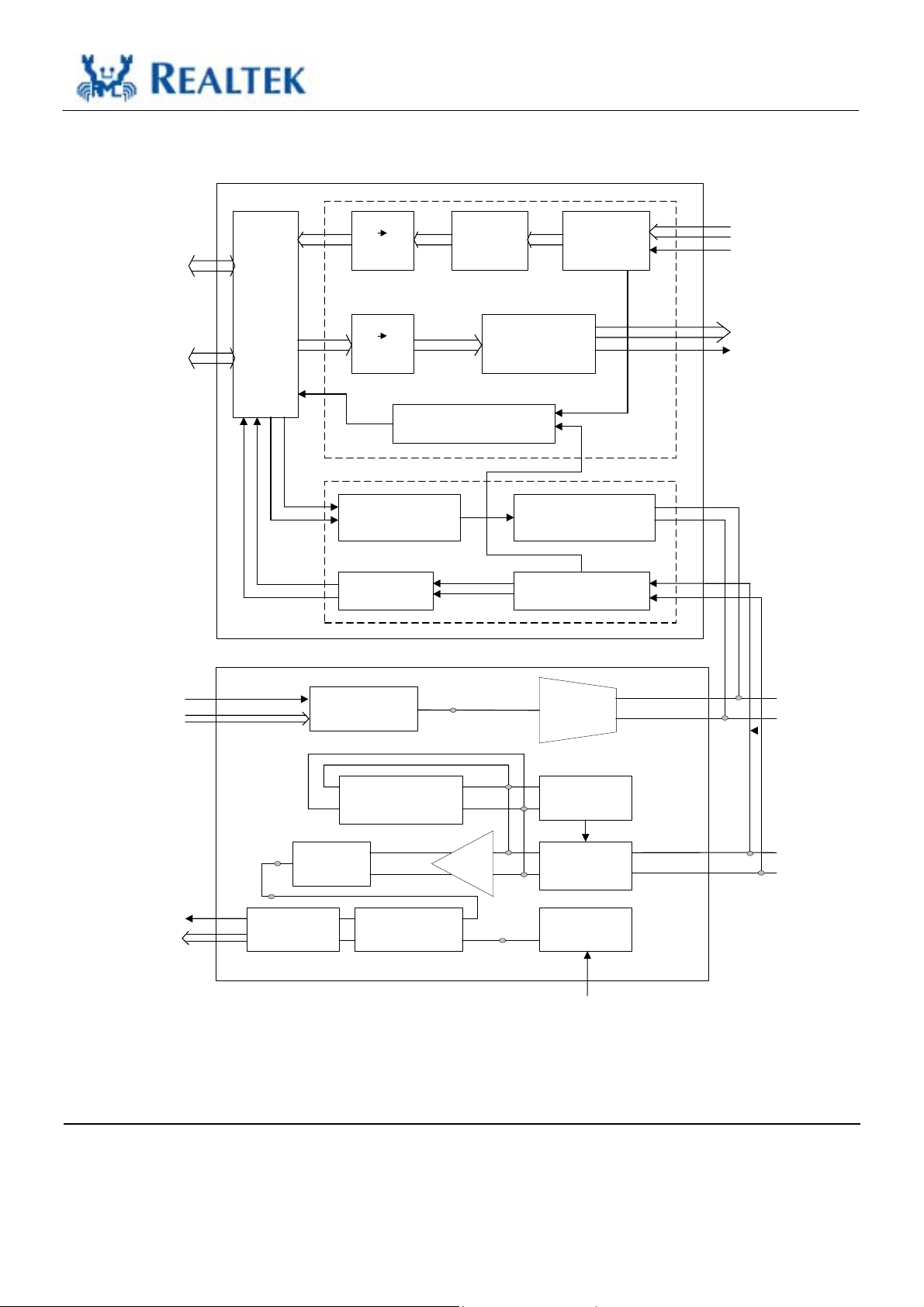
3. Block Diagram
100M
RTL8201CP
Datasheet
MII
Interface
SNI
Interface
10/100
half/full
Switch
Logic
TXC10
TXD10
RXC10
RXD10
5B 4B
Decoder
4B 5B
Encoder
10/100M Auto-negotiation
Data
Alignment
Control Logic
Descrambler
Scrambler
10M
Manchester coded
waveform
Data Recovery Receive low pass filter
10M Output waveform
shaping
RXD
RXC 25M
TXD
TXC 25M
Link pulse
TXC 25M
TXD
RXC 25M
RXD
Serial to
Parrallel
Parrallel
to Serial
Baseline
wander
Correction
MLT-3
to NRZI
ck
data
TD+
Variable Current
3 Level
Comparator
Slave
PLL
Control
Voltage
3 Level
Driver
Peak
Detect
Adaptive
Equalizer
Master
PPL
TXO+
TXO -
RXIN+
RXIN-
25M
Figure 1. Block Diagram
Single-Chip/Port 10/100 Fast Ethernet PHYceiver 2 Track ID: JATR-1076-21 Rev. 1.1
Page 8
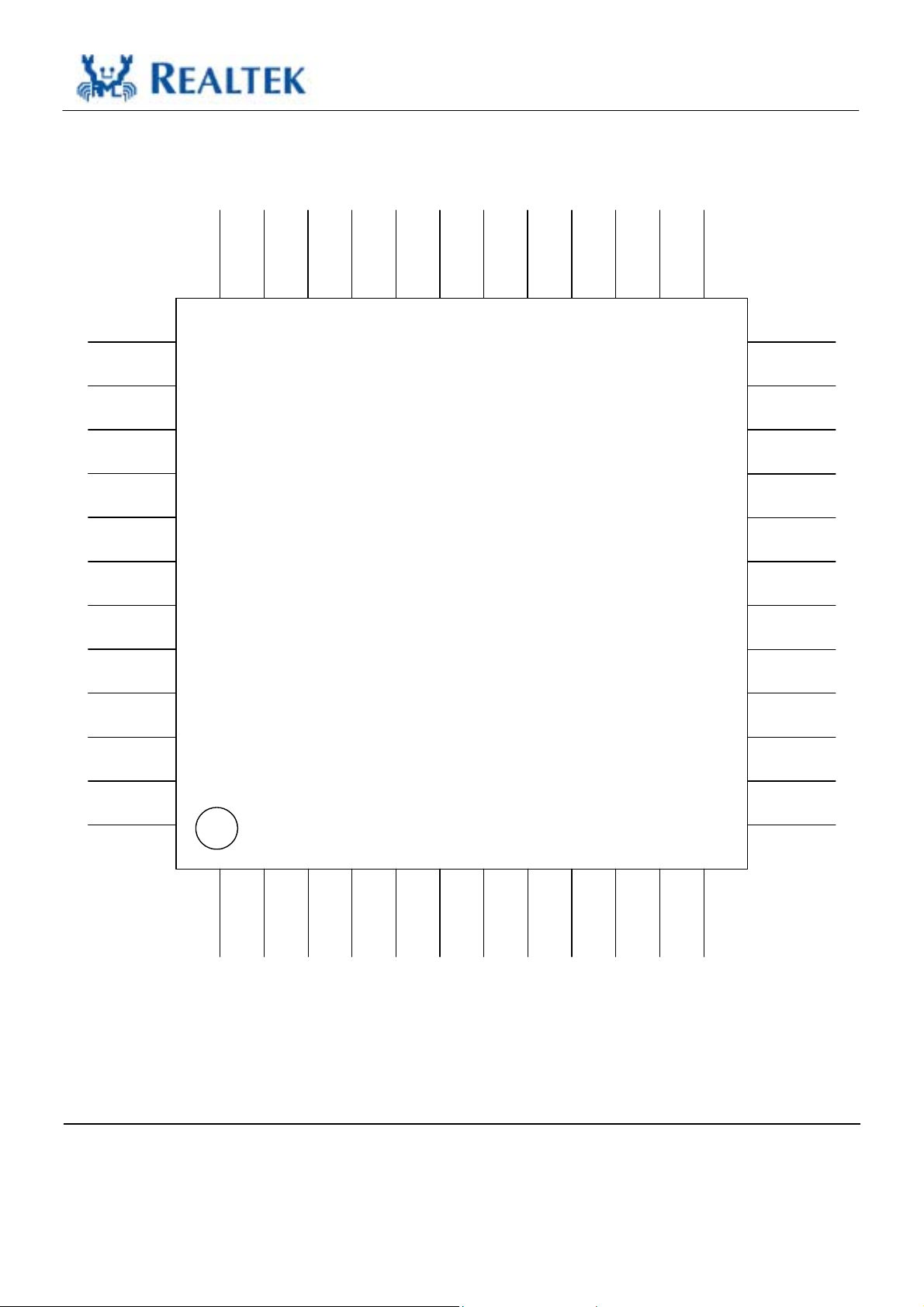
4. Pin Assignments
33. TPTX-
36. AVDD33
37. ANE
34. TPTX+
35. AGND
32. PWFBOUT
31. TPRX+
30. TPRX-
RTL8201CP
Datasheet
25. MDC
28. RTSET
29. AGND
26. MDIO
27. NC
24. RXER
/FXEN
38. DUPLEX
39. SPEED
40. RPTR
41. LDPS
42. RESETB
43. ISOLATE
44. MII/SN IB
45. DGND
46. X1
47. X2
48. DVDD33
RTL8201CP
23. CRS
22. RXDV
21. RXD0
20. RXD1
19. RXD2
18. RXD3
17. DGND
16. RXC
15. LED4/
PHYAD4
14. DVDD33
13. LED3/
PHYAD3
1. COL
2. TXEN
3. TXD3
4. TXD2
5. TXD1
6. TXD0
PHYAD1
PHYAD0
7. TXC
9. LED0/
8. PWFBIN
10. LED1/
11. DGND
12. LED2/
PHYAD2
Figure 2. Pin Assignments
Single-Chip/Port 10/100 Fast Ethernet PHYceiver 3 Track ID: JATR-1076-21 Rev. 1.1
Page 9

5. Pin Description
LI: Latched Input during Power up or Reset O: Output I: Input
IO: Bi-directional input and output P: Power
5.1. MII Interface
Table 1. MII Interface
Name Type Pin No. Description
TXC O 7 Transmit Clock.
This pin provides a continuous clock as a timing reference for TXD[3:0] and
TXEN.
TXEN I 2 Transmit Enable.
The input signal indicates the presence of valid nibble data on TXD[3:0].
TXD[3:0] I 3, 4, 5, 6 Transmit Data.
The MAC will source TXD[0..3] synchronous with TXC when TXEN is
asserted.
RXC O 16 Receive Clock.
This pin provides a continuous clock reference for RXDV and RXD[0..3]
signals. RXC is 25MHz in 100Mbps mode and 2.5Mhz in 10Mbps mode.
COL O 1 Collision Detect.
COL is asserted high when a collision is detected on the media.
CRS O 23 Carrier Sense.
This pin’s signal is asserted high if the media is not in IDEL state.
RXDV O 22 Receive Data Valid.
This pin’s signal is asserted high when received data is present on the
RXD[3:0] lines. The signal is de-asserted at the end of the packet. The signal is
valid on the rising edge of the RXC.
RXD[3:0] O 18, 19, 20, 21 Receive Data.
These are the four parallel receive data lines aligned on the nibble boundaries
driven synchronously to the RXC for reception by the external physical unit
(PHY).
RXER/
FXEN
MDC I 25 Management Data Clock.
MDIO IO 26 Management Data Input/Output.
O/LI 24 Receive Error.
If a 5B decode error occurs, such as invalid /J/K/, invalid /T/R/, or invalid
symbol, this pin will go high.
Fiber/UTP Enable.
During power on reset, this pin status is latched to determine the media mode to
operate in.
1: Fiber mode
0: UTP mode
An internal weak pull low resistor, sets this to the default of UTP mode. It is possible
to use an external 5.1KΩ pull high resistor to enable fiber mode.
After power on, the pin operates as the Receive Error pin.
This pin provides a clock synchronous to MDIO, which may be asynchronous
to the transmit TXC and receive RXC clocks. The clock rate can be up to
2.5MHz.
This pin provides the bi-directional signal used to transfer management
information.
RTL8201CP
Datasheet
Single-Chip/Port 10/100 Fast Ethernet PHYceiver 4 Track ID: JATR-1076-21 Rev. 1.1
Page 10

5.2. SNI (Serial Network Interface) 10Mbps Only
Table 2. SNI (Serial Network Interface) 10Mbps Only
Name Type Pin No. Description
COL O 1 Collision Detect.
RXD0 O 21 Received Serial Data.
CRS O 23 Carrier Sense.
RXC O 16 Receive Clock.
Resolved from received data.
TXD0 I 6 Transmit Serial Data.
TXC O 7 Transmit Clock
Generated by PHY.
TXEN I 2 Transmit Enable.
For MAC to indicate transmit operation.
5.3. Clock Interface
Table 3. Clock Interface
Name Type Pin No. Description
X2 O 47 25MHz Crystal Output.
This pin provides the 25MHz crystal output. It must be left open when an
external 25MHz oscillator drives X1.
X1 I 46 25MHz Crystal Input.
This pin provides the 25MHz crystal input. If a 25MHz oscillator is used, connect
X1 to the oscillator’s output (see 8.3 Crystal Characteristics, page 30 for clock
source specifications.
RTL8201CP
Datasheet
5.4. 10Mbps/100Mbps Network Interface
Table 4. 10Mbps/100Mbps Network Interface
Name Type Pin No. Description
TPTX+
TPTX-
RTSET I 28 Transmit Bias Resistor Connection.
TPRX+
TPRX-
Single-Chip/Port 10/100 Fast Ethernet PHYceiver 5 Track ID: JATR-1076-21 Rev. 1.1
O
O
34
33
I
I
31
30
Transmit Output.
Differential transmit output pair shared by 100Base-TX, 100Base-FX and
10Base-T modes. When configured as 100Base-TX, output is an MLT-3 encoded
waveform. When configured as 100Base-FX, the output is pseudo-ECL level.
This pin should be pulled to GND by a 2KΩ (1%) resistor to define driving
current for the transmit DAC. The resistance value may be changed, depending
on experimental results of the RTL8201CP.
Receive Input.
Differential receive input pair shared by 100Base-TX, 100Base-FX, and
10Base-T modes.
Page 11

RTL8201CP
5.5. Device Configuration Interface
Table 5. Device Configuration Interface
Name Type Pin No. Description
ISOLATE I 4 3 Set high to isolate the RTL8201CP from the MAC. This will also isolate the MDC/MDIO
management interface. In this mode, the power consumption is minimum. This pin can be
directly connected to GND or VCC.
RPTR I 40 Set high to put the RTL8201CP into repeater mode. This pin can be directly
connected to GND or VCC.
SPEED LI 39 This pin is latched to input during a power on or reset condition. Set high to put
the RTL8201CP into 100Mbps operation. This pin can be directly connected to GND
or VCC.
DUPLEX LI 38 This pin is latched to input during a power on or reset condition. Set high to
enab le full duplex. This pin can be directly connected to GND or VCC.
ANE LI 37 This pin is latched to input during a power on or reset condition. Set high to
enable Auto-negotiation mode, set low to force mode. This pin can be directly
connected to GND or VCC.
LDPS I 41 Set high to put the RTL8201CP into LDPS mode. This pin can be directly connected
to GND or VCC. See 7.7 Power Down, Link Down, Power Saving, and Isolati on
Mo des, page 20, for more information.
MII/SNIB LI/O 44 This pin is latched to input during a power on or reset condition. Pull high to set
the RTL8201CP into MII mode operation. Set low for SNI mode. This pin can be
directly connected to GND or VCC.
Datasheet
5.6. LED Interface/PHY Address Configuration
These five pins are latched into the RTL8201CP during power up reset to configure the PHY address
[0:4] used for the MII management register interface. In normal operation, after initial reset, they are used
as driving pins for status indicator LEDs. The driving polarity, active low or active high, is determined by
each latched status of the PHY address [4:0] during power-up reset. If the latched status is High, then it
will be active low. If the latched status is Low, then it will be active high. See section 7.5 LED and PHY
Address Configuration, page 19, for more information.
Table 6. LED Interface/PHY Address Configuration
Name Type Pin No. Description
PHYAD0/
LED0
PHYAD1/
LED1
PHYAD2/
LED2
PHYAD3/
LED3
PHYAD4/
LED4
LI/O 9 PHY Address [0].
Link LED.
Lit when linked.
LI/O 10 PHY Address [1].
Full Duplex LED.
Lit when in Full Duplex operation.
LI/O 12 PHY Address [2].
10 ACT LED.
Blinking when transmitting or receiving data in 10Base-T mode.
LI/O 13 PHY Address [3].
ACT LED.
Blinking when transmitting or receiving data at 100Base-T or Fiber Mode.
LI/O 15 PHY Address [4].
Collision LED.
Blinks when collisions occur.
Single-Chip/Port 10/100 Fast Ethernet PHYceiver 6 Track ID: JATR-1076-21 Rev. 1.1
Page 12

5.7. Power and Ground Pins
Table 7. Power and Ground Pins
Name Type Pin No. Description
AVDD33 P 36 3.3V Analog power input.
3.3V power supply for analog circuit; should be well decoupled.
AGND P 29, 35 Analog Ground.
Should be connected to a larger GND plane.
DVDD33 P 14, 48 3.3V Digital Power input.
3.3V power supply for digital circuit.
DGND P 11, 17, 45 Digital Ground.
Should be connected to a larger GND plane.
5.8. Reset and Other Pins
Table 8. Reset and Other Pins
Name Type Pin No. Description
RESETB I 42 RESETB
Set low to reset the chip. For a complete reset, this pin must be asserted low
for at least 10ms.
PWFBOUT O 32 Power Feedback Output.
Be sure to connect a 22uF tantalum capacitor for frequency compensation and
a 0.1uF capacitor for noise de-coupling. Then connect this pin through a
ferrite bead to PWFBIN (pin8). The connection method is outlined in
7.11 3.3V Power Supply and Voltage Conversion Circuit, page 22..
PWFBIN I 8 Power Feedback Input: see the PWFBOUT description above.
NC 27 Not Connected.
RTL8201CP
Datasheet
Single-Chip/Port 10/100 Fast Ethernet PHYceiver 7 Track ID: JATR-1076-21 Rev. 1.1
Page 13

RTL8201CP
Datasheet
6. Register Descriptions
This section describes the functions and usage of the registers available in the RTL8201CP.
In this section the following abbreviations are used:
RO: Read Only
RW: Read/Write
6.1. Register 0 Basic Mode Control Register
Table 9. Register 0 Basic Mode Control Register
Address Name Description Mode Default
0:15 Reset This bit sets the status and control registers of the PHY in a default
state. This bit is self-clearing.
1: Software reset
0: Normal operation
0:14 Loopback This bit enables loopback of transmit data nibbles TXD3:0 to the
receive data path.
1: Enable loopback
0: Normal operation
0:13 Spd_Set This bit sets the network speed.
1: 100Mbps
0: 10Mbps
After completing auto negotiation, this bit will reflect the Speed status.
1: 100Base-T
0: 10Base-T)
When 100Base-FX mode is enabled, this bit=1 and is read only.
0:12 Auto
Negotiation
Enable
0:11 Power Down This bit turns down the power of the PHY chip, including the internal
0:10 Reserved
0:9 Restart Auto
Negotiation
0:8 Duplex
Mode
0:7:0 Reserved
This bit enables/disables the Nway auto-negotiation function.
1: Enable auto-negotiation; bits 0:13 and 0:8 will be ignored.
0: Disable auto-negotiation; bits 0:13 and 0:8 will determine the link
speed and the data transfer mode, respectively.
When 100Base-FX mode is enabled, this bit=0 and is read only.
crystal oscillator circuit. The MDC, MDIO is still alive for accessing
the MAC.
1: Power down
0: Normal operation
This bits allows the NWay auto-negotiation function to be reset.
1: Re-start auto-negotiation
0: Normal operation
This bit sets the duplex mode if auto-negotiation is disabled
(bit 0:12=0).
1: Full duplex
0: Half duplex
After completing auto-negotiation, this bit will reflect the duplex
status.
1: Full duplex
0: Half duplex
RW
RW 0
RW 1
RW 1
RW 0
RW 0
RW 1
0
Single-Chip/Port 10/100 Fast Ethernet PHYceiver 8 Track ID: JATR-1076-21 Rev. 1.1
Page 14
RTL8201CP
Datasheet
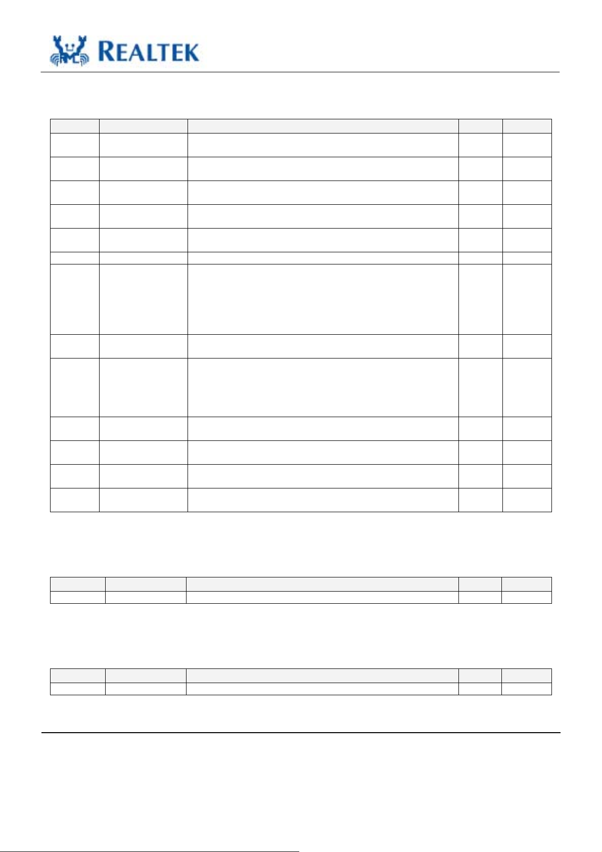
6.2. Register 1 Basic Mode Status Register
Table 10. Register 1 Basic Mode Status Register
Address Name Description Mode Default
1:15 100Base-T4 1: Enable 100Base-T4 support
0: Suppress 100Base-T4 support
1:14 100Base_TX_ FD 1: Enable 100Base-TX full duplex support
0: Suppress 100Base-TX full duplex support
1:13 100BASE_TX_HD 1: Enable 100Base-TX half duplex support
0: Suppress 100Base-TX half duplex support
1:12 10Base_T_FD 1: Enable 10Base-T full duplex support
0: Suppress 10Base-T full duplex support
1:11 10_Base_T_HD 1: Enable 10Base-T half duplex support
0: Suppress 10Base-T half duplex support
1:10~7 Reserved
1:6 MF Preamble
Suppression
1:5 Auto Negotiation
Complete
1:4 Remote Fault 1: Remote fault condition detected (cleared on read)
1:3 Auto Negotiation 1: Link has not experienced fail state
1:2 Link Status 1: Valid link established
1:1 Jabber Detect 1: Jabber condition detected
1:0 Extended Capability 1: Extended register capability
The RTL8201CP will accept management frames with
preamble suppressed.
A minimum of 32 preamble bits are required for the first SMI
read/write transaction after reset. One idle bit is required
between any two management transactions as per IEEE 802.3u
specifications
1: Auto-negotiation process completed
0: Auto-negotiation process not completed
0: No remote fault condition detected
When in 100Base-FX mode, this bit means an in-band signal
Far-End-Fault has been detected (See 7.12 Far End Fault
Indication, page 22.
0: Link experienced fail state
0: No valid link established
0: No jabber condition detected
0: Basic register capability only
RO 0
RO 1
RO 1
RO 1
RO 1
RO 1
RO 0
RO 0
RO 1
RO 0
RO 0
RO 1
6.3. Register 2 PHY Identifier Register 1
Table 11. Register 2 PHY Identifier Register 1
Address Name Description Mode Default
2:15~0 PHYID1 PHY identifier ID for software recognition of the RTL8201CP RO 0000
6.4. Register 3 PHY Identifier Register 2
Table 12. Register 3 PHY Identifier Register 2
Address Name Description Mode Default
3:15~0 PHYID2 PHY identifier ID for software recognition of the RTL8201CP RO 8201
Single-Chip/Port 10/100 Fast Ethernet PHYceiver 9 Track ID: JATR-1076-21 Rev. 1.1
Page 15
RTL8201CP
Datasheet
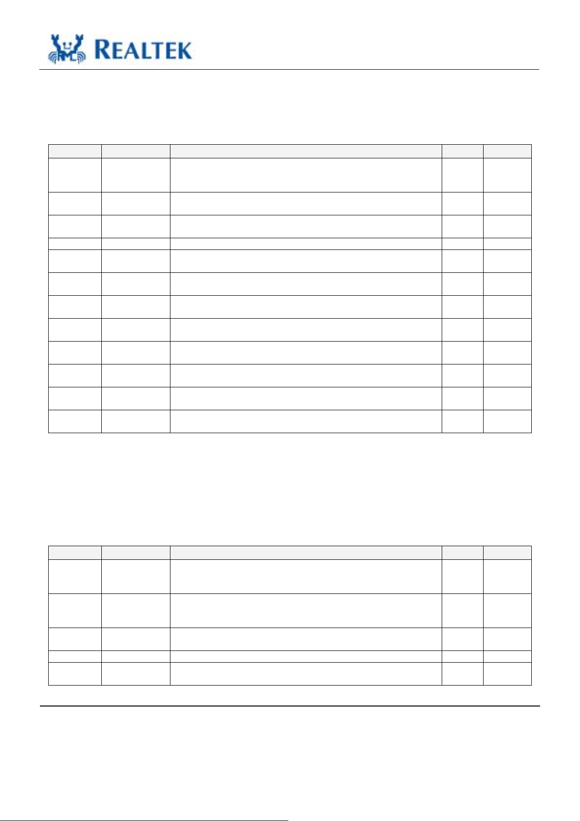
6.5. Register 4 Auto-Negotiation Advertisement Register (ANAR)
This register contains the advertised abilities of this device as they will be transmitted to its link partner
during auto-negotiation.
Address Name Description Mode Default
4:15 NP Next Page bit.
4:14 ACK 1: Acknowledge reception of link partner capability data word
4:13 RF 1: Advertise remote fault detection capability
4:12 Reserved
4:11 TXFC 1: TX flow control is supported by local node
4:10 RXFC 1: RX flow control is supported by local node
4:9 T4 1: 100Base-T4 is supported by local node
4:8 TXFD 1: 100Base-TX full duplex is supported by local node
4:7 TX 1: 100Base-TX is supported by local node
4:6 10FD 1: 10Base-T full duplex supported by local node
4:5 10 1: 10Base-T is supported by local node
4:4~0 Selector Binary encoded selector supported by this node. Currently only
Table 13. Register 4 Auto-Negotiation Advertisement Register (ANAR)
RO 0
0: Transmitting the primary capability data page
1: Transmitting the protocol specific data page
RO 0
0: Do not acknowledge reception
RW 0
0: Do not advertise remote fault detection capability
RW 0
0: TX flow control not supported by local node
RW 0
0: RX flow control not supported by local node
RO 0
0: 100Base-T4 not supported by local node
RW 1
0: 100Base-TX full duplex not supported by local node
RW 1
0: 100Base-TX not supported by local node
RW 1
0: 10Base-T full duplex not supported by local node
RW 1
0: 10Base-T not supported by local node
RW 00001
CSMA/CD 00001 is specified. No other protocols are supported.
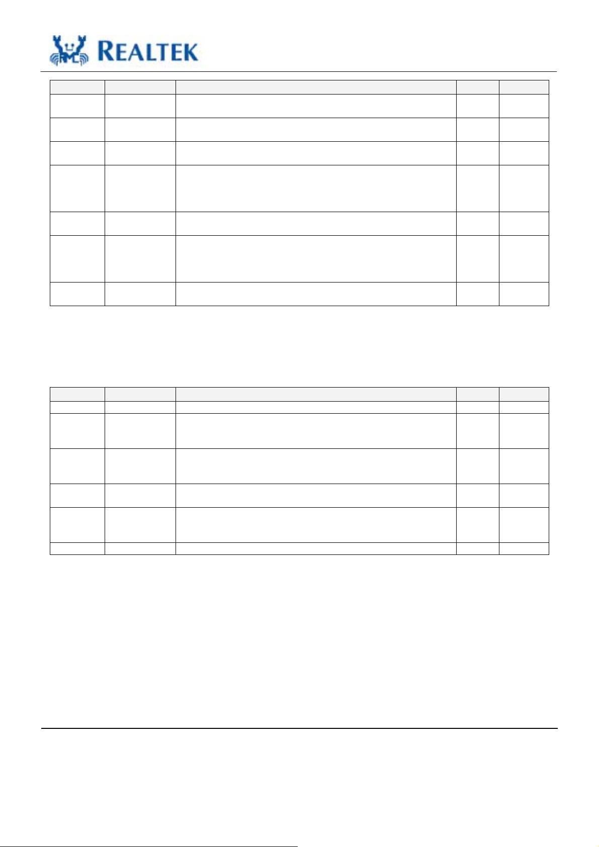
6.6. Register 5 Auto-Negotiation Link Partner Ability Register
(ANLPAR)
This register contains the advertised abilities of the Link Partner as received during auto-negotiation. The
content changes after a successful auto-negotiation if Next-pages are supported.
Table 14. Register 5 Auto-Negotiation Link Partner Ability Register (ANLPAR)
Address Name Description Mode Default
5:15 NP Next Page bit.
0: Transmitting the primary capability data page
1: Transmitting the protocol specific data page
5:14 ACK 1: Link partner acknowledges reception of local node’s capability
data word
0: No acknowledgement
5:13 RF 1: Link partner is indicating a remote fault
0: Link partner does not indicate a remote fault
5:12 Reserved
5:11 TXFC 1: TX flow control is supported by Link partner
0: TX flow control not supported by Link partner
Single-Chip/Port 10/100 Fast Ethernet PHYceiver 10 Track ID: JATR-1076-21 Rev. 1.1
RO 0
RO 0
RO 0
RO 0
Page 16
RTL8201CP
Datasheet
Address Name Description Mode Default
5:10 RXFC 1: RX flow control is supported by Link partner
0: RX flow control not supported by Link partner
5:9 T4 1: 100Base-T4 is supported by link partner
0: 100Base-T4 not supported by link partner
5:8 TXFD 1: 100Base-TX full duplex is supported by link partner
0: 100Base-TX full duplex not supported by link partner
5:7 100BASE-TX 1: 100Base-TX is supported by link partner
0: 100Base-TX not supported by link partner
This bit will also be set if the link in 100Base is established by
parallel detection.
5:6 10FD 1: 10Base-T full duplex is supported by link partner
0: 10Base-T full duplex not supported by link partner
5:5 10Base-T 1: 10Base-T is supported by link partner
0: 10Base-T not supported by link partner
This bit will also be set if the link in 10Base-T is established by
parallel detection.
5:4~0 Selector Link Partner’s binary encoded node selector Currently only
CSMA/CD 00001 is specified
RO 0
RO 0
RO 0
RO 1
RO 0
RO 0
RO 00000
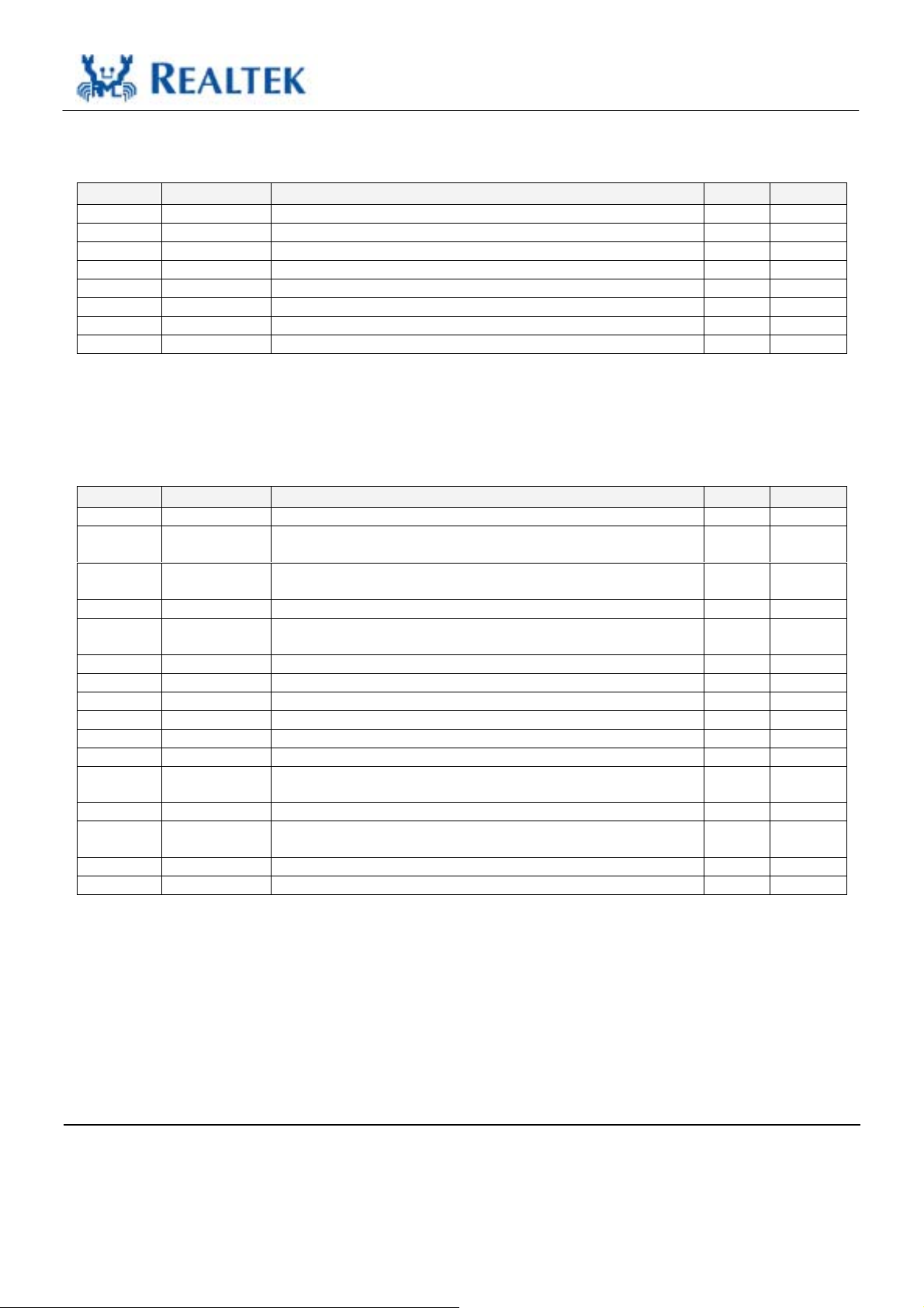
6.7. Register 6 Auto-Negotiation Expansion Register (ANER)
This register contains additional status for NWay auto-negotiation.
Table 15. Register 6 Auto-Negotiation Expansion Register (ANER)
Address Name Description Mode Default
6:15~5 Reserved This bit is permanently set to 0.
6:4 MLF Indicates whether a multiple link fault has occurred.
1: Fault occurred
0: No fault occurred
6:3 LP_NP_ABLE Indicates whether the link partner supports Next Page negotiation.
1: Supported
0: Not supported
6:2 NP_ABLE This bit indicates whether the local node is able to send additional
Next Pages. Internal use only
6:1 PAGE_RX This bit is set when a new Link Code Word Page has been
received. It is automatically cleared when the auto-negotiation
link partner’s ability register (register 5) is read by management.
6:0 LP_NW_ABLE 1: Link partner supports NWay auto-negotiation. RO 0
RO 0
RO 0
RO 0
RO 0
Single-Chip/Port 10/100 Fast Ethernet PHYceiver 11 Track ID: JATR-1076-21 Rev. 1.1
Page 17
RTL8201CP
Datasheet
6.8. Register 16 NWay Setup Register (NSR)
Table 16. Register 16 NWay Setup Register (NSR)
Address Name Description Mode Default
16:15~12 Reserved
16:11 ENNWLE 1: LED4 Pin indicates linkpulse RW 0
16:10 Testfun 1: Auto-negotiation speeds up internal timer RW 0
16:9 NWLPBK 1: Set NWay to loopback mode. RW 0
16:8~3 Reserved
16:2 FLAGABD 1: Auto-negotiation experienced ability detect state RO 0
16:1 FLAGPDF 1: Auto-negotiation experienced parallel detection fault state RO 0
16:0 FLAGLSC 1: Auto-negotiation experienced link status check state RO 0
6.9. Register 17 Loopback, Bypass, Receiver Error Mask Register (LBREMR)
Table 17. Register 17 Loopback, Bypass, Receiver Error Mask Register (LBREMR)
Address Name Description Mode Default
17:15 RPTR Set to 1 to put the RTL8201CP into repeater mode RW 0
17:14 BP_4B5B Assertion of this bit allows bypassing of the 4B/5B & 5B/4B
encoder.
17:13 BP_SCR Assertion of this bit allows bypassing of the
scrambler/descrambler.
17:12 LDPS Set to 1 to enable Link Down Power Saving mode RW 0
17:11 AnalogOFF Set to 1 to power down analog function of transmitter and
receiver.
17:10 Reserve Reserved.
17:9 LB Set to 1 to enable DSP Loopback. RW 0
17:8 F_Link_10 Used to logic force good link in 10Mbps for diagnostic purposes. RW 1
17:7 F_Link_100 Used to logic force good link in 100Mbps for diagnostic purposes. RW 1
17:6 JBEN Set to 1 to enable Jabber Function in 10Base-T RW 0
17:5 CODE_err Assertion of this bit causes a code error detection to be reported. RW 0
17:4 PME_err Assertion of this bit causes a pre-mature end error detection to be
reported.
17:3 LINK_err Assertion of this bit causes a link error detection to be reported. RW 0
17:2 PKT_err Assertion of this bit causes a ‘detection of packet errors due to
722 ms time-out’ to be reported.
17:1 FXMODE This bit indicates whether Fiber Mode is Enabled. RO 0
17:0 RMIIMODE This bit indicates whether RMII mode is Enabled. RO 0
RW 0
RW 0
RW 0
RW 0
RW 0
Single-Chip/Port 10/100 Fast Ethernet PHYceiver 12 Track ID: JATR-1076-21 Rev. 1.1
Page 18
RTL8201CP
Datasheet
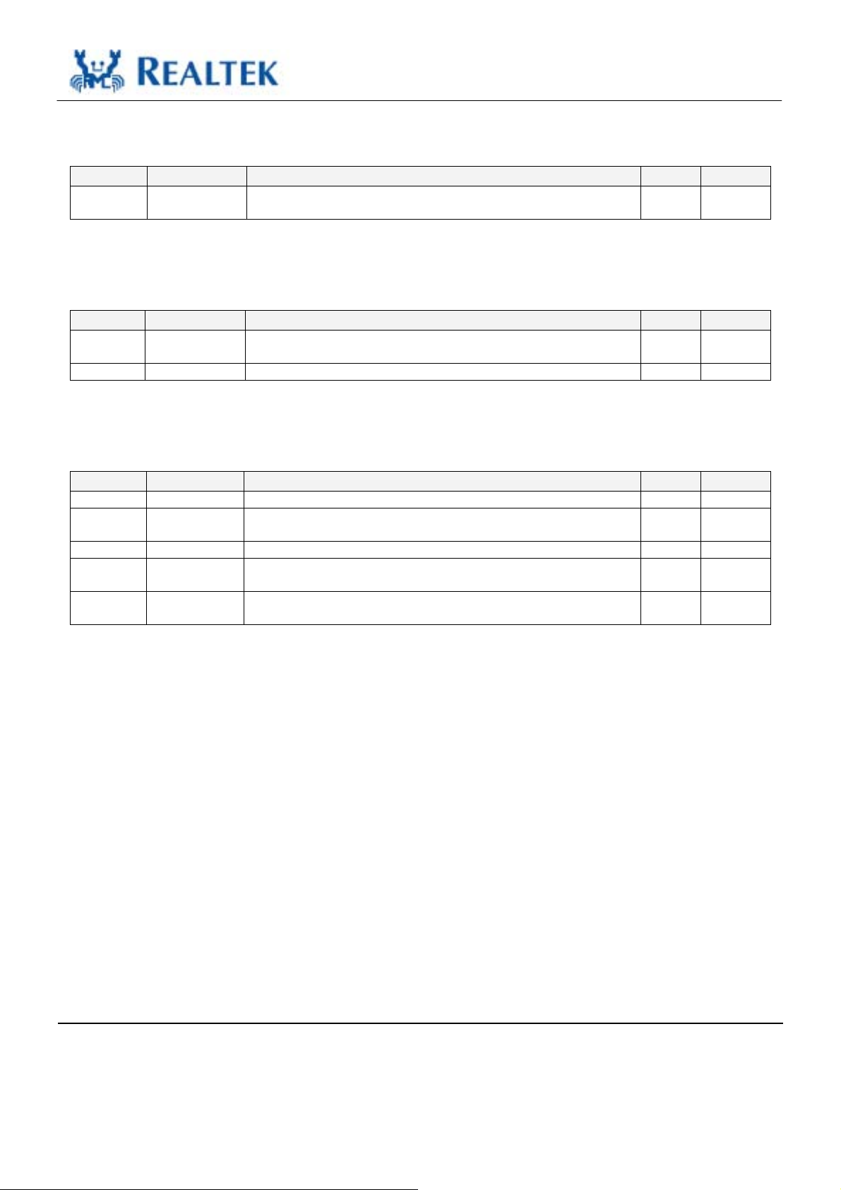
6.10. Register 18 RX_ER Counter (REC)
Table 18. Register 18 RX_ER Counter (REC)
Address Name Description Mode Default
18:15~0 RXERCNT This 16-bit counter increments by 1 for each valid packet
received.
RW H’[0000]
6.11. Register 19 SNR Display Register
Table 19. Register 19 SNR Display Register
Address Name Description Mode Default
19:15~4 Reserved Realtek Test Mode Internal use. Do not change this field without
Realtek’s approval.
19:3~0 SNR These 4-bits show the Signal to Noise Ratio value. RW 0000
6.12. Register 25 Test Register
Table 20. Register 25 Test Register
Address Name Description Mode Default
25:15~12 Test Reserved for internal testing. RW
25:11~7 PHYAD[4:0] Reflects the PHY address defined by external PHY address
configuration pins.
25:6~2 Test Reserved for internal testing. RO
25:1 LINK10 1: 10Base-T link established
0: No 10Base-T link established
25:0 LINK100 1: 100Base-FX or 100Base-TX link established
0: No 100Base link established
RO
RO
RO
Single-Chip/Port 10/100 Fast Ethernet PHYceiver 13 Track ID: JATR-1076-21 Rev. 1.1
Page 19

RTL8201CP
Datasheet
7. Functional Description
The RTL8201CP PHYceiver is a physical layer device that integrates 10Base-T and 100BaseTX/100Base-FX functions and some extra power management features into a 48-pin single chip that is
used in 10/100 Fast Ethernet applications. This device supports the following functions:
• MII interface with MDC/MDIO SMI management interface to communicate with MAC
• IEEE 802.3u clause 28 Auto-Negotiation ability
• Flow control ability support to cooperate with MAC
• Speed, duplex, auto-negotiation ability configurable by hard wire or MDC/MDIO
• Flexible LED configuration
• 7-wire SNI (Serial Network Interface) support (only in 10Mbps mode)
• Power Down mode support
• 4B/5B transform
• Scrambling/De-scrambling
• NRZ to NRZI, NRZI to MLT-3
• Manchester Encode and Decode for 10Base-T operation
• Clock and Data recovery
• Adaptive Equalization
• Far End Fault Indication (FEFI) in fiber mode
7.1. MII and Management Interface
7.1.1. Data Transition
To set the RTL8201CP for MII mode operation, pull MII/SNIB pin high and set the ANE, SPEED, and
DUPLEX pins.
The MII (Media Independent Interface) is an 18-signal interface (as described in IEEE 802.3u) supplying
a standard interface between the PHY and MAC layer. This interface operates at two frequencies –
25Mhz and 2.5Mhz to support 100Mbps/10Mbps bandwidth for both transmit and receive functions.
Transmission
The MAC asserts the TXEN signal. It then changes byte data into 4-bit nibbles and passes them to the
PHY via TXD[0..3]. The PHY will sample TXD[0..3] synchronously with TXC — the transmit clock
signal supplied by PHY – during the interval TXEN is asserted.
Reception
The PHY asserts the RXEN signal. It passes the received nibble data RXD[0..3] clocked by RXC. CRS
and COL signals are used for collision detection and handling.
In 100Base-TX mode, when the decoded signal in 5B is not IDLE, the CRS signal will assert. When 5B is
recognized as IDLE it will be de-asserted. In 10Base-T mode, CRS will assert when the 10M preamble
has been confirmed and will be de-asserted when the IDLE pattern has been confirmed.
Single-Chip/Port 10/100 Fast Ethernet PHYceiver 14 Track ID: JATR-1076-21 Rev. 1.1
Page 20
RTL8201CP
Datasheet
The RXDV signal will be asserted when decoded 5B are /J/K/ and will be de-asserted if the 5B are /T/R/
or IDLE in 100Mbps mode. In 10Mbps mode, the RXDV signal is the same as the CRS signal.
The RXER (Receive Error) signal will be asserted if any 5B decode errors occur such as invalid J/K,
invalid T/R, or invalid symbol. This pin will go high for one or more clock periods to indicate to the
reconciliation sublayer that an error was detected somewhere in the frame.
Note: The RTL8201CP does not use a TXER signal. This does not affect the transmit function.
7.1.2. Serial Management
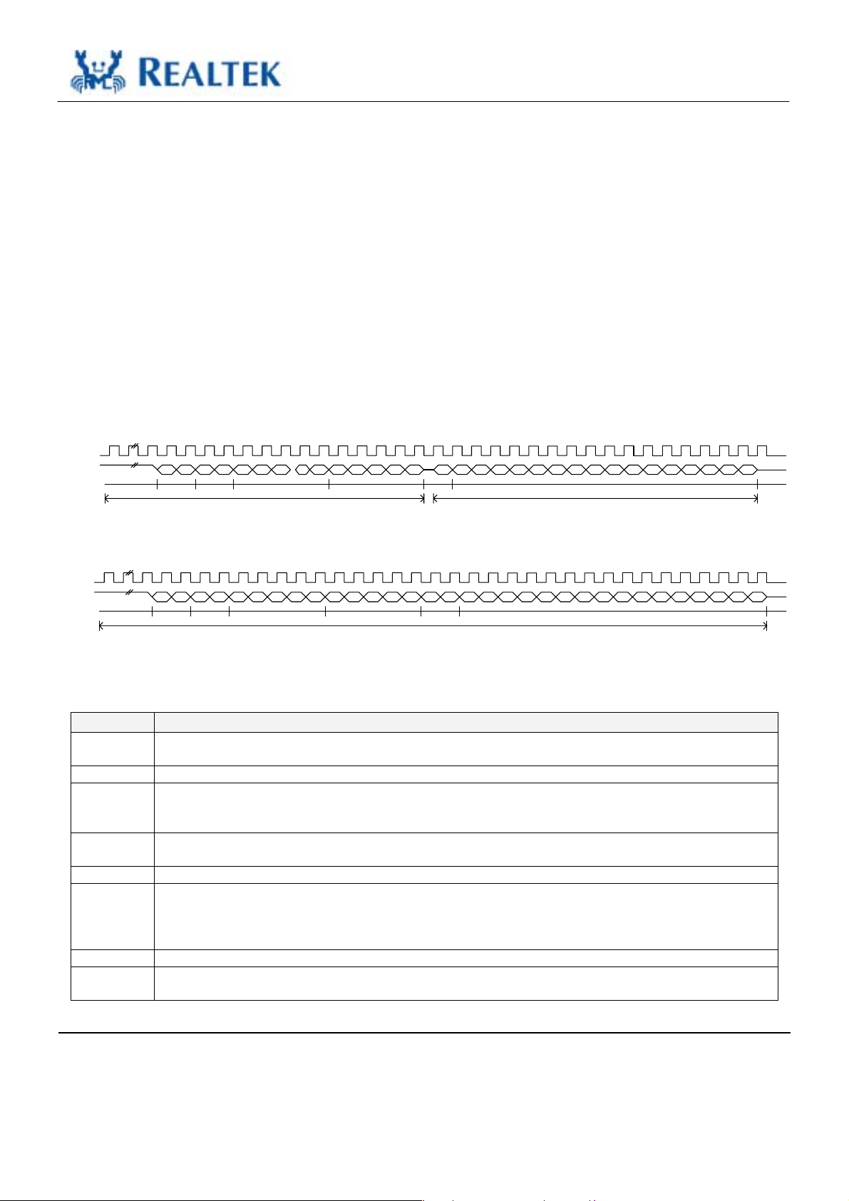
The MAC layer device can use the MDC/MDIO management interface to control a maximum of 31
RTL8201CP devices, configured with different PHY addresses (00001b to 11111b). During a hardware
reset, the logic levels of pins 9, 10, 12, 13, 15 are latched into the RTL8201CP to be set as the PHY
address for management communication via the serial interface. Setting the PHY address to 00000b will
put the RTL8201CP into power down mode. The read and write frame structure for the management
interface is illustrated in Figure 3 and Figure 4.
MDC
MDIO
32 1s
OPSTPreamble PHYAD[4:0] TA DATAREGAD[4:0] Idle
MDIO is sourced by MAC. Clock data into PHY on rising edge of MDC
Figure 3. Read Cycle
Z
D14
D15
D13 D12 D11 D10
MDIO is sourced by PHY. Clock data from PHY on rising edge of MDC
D9 D8 D7 D6 D5 D4 D3 D2 D1 D0A4 A3 A2 A1 A0 R4 R3 R2 R1 R00110 0
MDC
MDIO
32 1s
A4 A3 A2 A1 A0 R4 R3 R2 R1 R01010 1 0
OP
STPreamble
PHYAD[4:0]
MDIO is sourced by MAC. Clock data into PHY on rising edge of MDC
TA
D15
D14
D13 D12
D11
D10
D9
D8 D7 D6
DATAREGAD[4:0]
D5
D4 D3 D2
Figure 4. Write Cycle
Table 21. Serial Management
Name Description
Preamble 32 contiguous logical ‘1’s sent by the MAC on MDIO along with 32 corresponding cycles on MDC. This
provides synchronization for the PHY.
ST Start of Frame. Indicated by a 01 pattern.
OP Operation Code.
Read: 10
Write: 01
PHYAD PHY Address. Up to 31 PHYs can be connected to one MAC. This 5-bit field selects which PHY the
frame is directed to.
REGAD Register Address. This is a 5-bit field that sets which of the 32 registers of the PHY this operation refers to.
TA Turnaround. This is a 2-bit time-spacing between the register address and the data field of a frame to
avoid contention during a read transaction. For a read transaction, both the STA and the PHY shall remain
in a high-impedance state for the first bit time of the turnaround. The PHY shall drive a zero bit during
the second bit time of the turnaround of a read transaction.
DATA Data. These are the 16 bits of data.
IDLE Idle Condition. Not truly part of the management frame. This is a high impedance state. Electrically, the
PHY’s pull-up resistor will pull the MDIO line to a logical ‘1’.
D1 D0
Idle
Single-Chip/Port 10/100 Fast Ethernet PHYceiver 15 Track ID: JATR-1076-21 Rev. 1.1
Page 21
RTL8201CP
Datasheet
7.2. Auto-Negotiation and Parallel Detection
The RTL8201CP supports IEEE 802.3u clause 28 Auto-negotiation for operation with other transceivers
supporting auto-negotiation. The RTL8201CP can auto detect the link partner’s abilities and determine
the highest speed/duplex configuration possible between the two devices. If the link partner does not
support auto-negotiation, then the RTL8201CP will enable half duplex mode and enter parallel detection
mode. The RTL8201CP will default to transmit FLP (Fast Link Pulse) and wait for the link partner to
respond. If the RTL8201CP receives FLP, then the auto-negotiation process will go on. If it receives NLP
(Normal Link Pulse), then the RTL8201CP will change to 10Mbps and half duplex mode. If it receives a
100Mbps IDLE pattern, it will change to 100Mbps and half duplex mode.
To enable auto-negotiation mode operation on the RTL8201CP, just pull the ANE (Auto-Negotiation
Enable) pin high. The SPEED and DUPLEX pins will set the ability content of the auto-negotiation
register. Auto-negotiation mode can be externally disabled by pulling the ANE pin low. In this case, the
SPEED pin and DUPLEX pin will change the media configuration of the RTL8201CP.
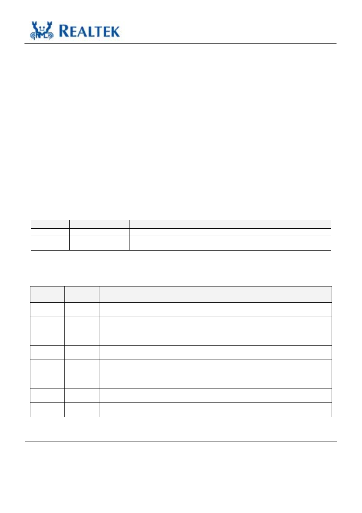
Below is a list of all configurations of the ANE/SPEED/DUPLEX pins and their operation in Fiber or
UTP mode.
7.2.1. Setting the Medium Type and Interface Mode to MAC
Table 22. Setting the Medium Type and Interface Mode to MAC
FX (Pin 24) MII/SNIB (P in 44) Operation Mode
L H UTP mode and MII interface.
L L UTP mode and SNI interface.
H X Fiber mode and MII interface.
7.2.2. UTP Mode and MII Interface
Table 23. UTP Mode and MII Interface
ANE
(Pin 37)
H L L
H L H
H H L
H H H
L L L
L L H
L H L
L H H
SPEED
(Pin 39)
DUPLEX
(Pin 38)
Operation
Auto-negotiation enabled. The ability field does not support 100Mbps or
full duplex mode operation.
Auto-negotiation enabled. The ability field does not support 100Mbps
operation.
Auto-negotiation enabled. The ability field does not support full duplex
mode operation.
Default setup, auto-negotiation enabled. The RTL8201CP supports 10BaseT /100Base-TX, half/full duplex mode operation.
Auto-negotiation disabled. Forces the RTL8201CP into 10Base-T and half
duplex mode.
Auto-negotiation disabled. Forces the RTL8201CP into 10Base-T and full
duplex mode.
Auto-negotiation disabled. Forces the RTL8201CP into 100Base-TX and half
duplex mode.
Auto-negotiation disabled. Forces the RTL8201CP into 100Base-TX and full
duplex mode.
Single-Chip/Port 10/100 Fast Ethernet PHYceiver 16 Track ID: JATR-1076-21 Rev. 1.1
Page 22
RTL8201CP
Datasheet
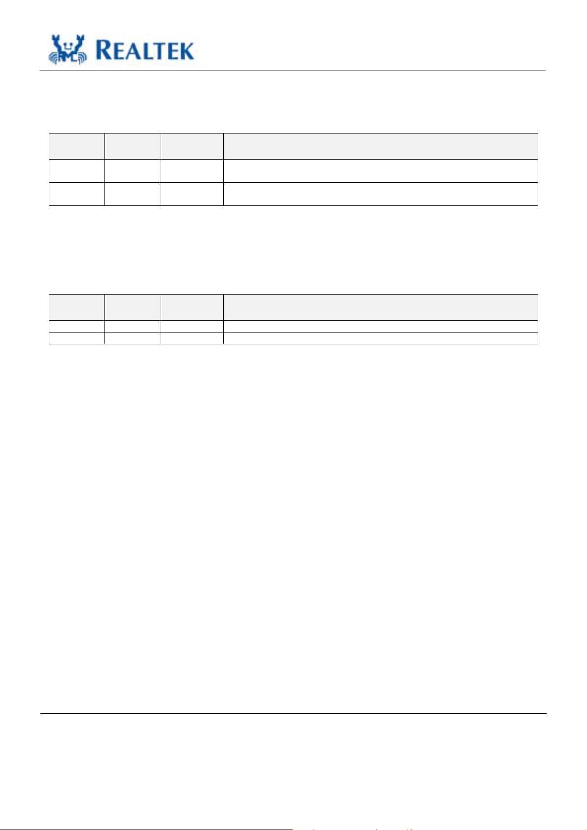
7.2.3. UTP Mode and SNI Interface
SNI interface to MAC (only operates in 10Base-T when the SNI interface is enabled)
Table 24. UTP Mode and SNI Interface
ANE
(Pin 37)
X X L The duplex pin is pulled low to support the 10Base-T half duplex function.
X X H The RTL8201CP also supports full duplex in SNI mode. The duplex pin is
SPEED
(Pin 39)
DUPLEX
(Pin 38)
Operation
10Base-T half duplex is the specified default mode in the SNI interface.
pulled high to support 10Base-T full duplex function.
7.2.4. Fiber Mode and MII Interface
The RTL8201CP only supports 100Base-FX when Fiber mode is enabled. ANE (Auto-Negotiation
Enable) and SPEED configuration is ignored when Fiber mode is enabled.
Table 25. Fiber Mode and MII Interface
ANE
(Pin 37)
X X H The duplex pin is pulled high to support 100Base-FX full duplex function.
X X L The duplex pin is pulled low to support 100Base-FX half duplex function.
SPEED
(Pin 39)
DUPLEX
(Pin 38)
Operation
7.3. Flow Control Support
The RTL8201CP supports flow control indications. The MAC can program the MII register to indicate to
the PHY that flow control is supported. When the MAC supports the Flow Control mechanism, setting
bit 10 of the ANAR register using the MDC/MDIO SMI interface, then the RTL8201CP will add the
ability to its NWay ability. If the Link partner also supports Flow Control, then the RTL8201CP can
recognize the Link partner’s NWay ability by examining bit 10 of ANLPAR (register 5).
Single-Chip/Port 10/100 Fast Ethernet PHYceiver 17 Track ID: JATR-1076-21 Rev. 1.1
Page 23

RTL8201CP
Datasheet
7.4. Hardware Configuration and Auto-Negotiation
This section describes methods to configure the RTL8201CP and set the auto-negotiation mode. This list
shows the various pins and their settings.
Table 26. Auto-Negotiation Mode Pin Settings
Pin Name Description
Isolate Set high to isolate the RTL8201CP from the MAC. This will also isolate the MDC/MDIO
management interface. In this mode, power consumption is minimum (see 7.7 Power Down, Link
Down, Power Saving, and Isolation Modes, page 20).
RPTR Pull high to set the RTL8201CP into repeater mode. This pin is pulled low by default (see
7.9 Repeater Mode Operation, page 22.
LDPS Pull high to set the RTL8201CP into LDPS mode. This pin is pulled low by default (see 7.7 Power
Down, Link Down, Power Saving, and Isolation Modes, page 20).
MII/SNIB Pull high to set RTL8201CP into MII mode operation, which is the default mode for the RTL8201.
This pin pulled low will set the RTL8201CP into SNI mode operation. When set to SNI mode, the
RTL8201CP will operate at 10Mbps (see 7.6 Serial Network Interface, page 20).
ANE Auto-Negotiation Enable. Pull high to enable auto-negotiation (default). Pull low to disable auto-
negotiation and activate the parallel detection mechanism (see 7.2 Auto-Negotiation and Parallel
Detection, page 16).
SPEED When ANE is pulled high, the ability to adjust speed is setup. When ANE is pulled low, pull this pin
low to force 10Mbps operation and high to force 100Mbps operation (see 7.2 Auto-Negotiation and
Parallel Detection, page 16).
DUPLEX When ANE is pulled high, the ability to adjust the DUPLEX pin will be setup. When ANE is pulled
low, pull this pin low to force half duplex and high to force full duplex operation (see 7.2 AutoNegotiation and Parallel Detection, page 16).
Single-Chip/Port 10/100 Fast Ethernet PHYceiver 18 Track ID: JATR-1076-21 Rev. 1.1
Page 24
RTL8201CP
Datasheet
7.5. LED and PHY Address Configuration
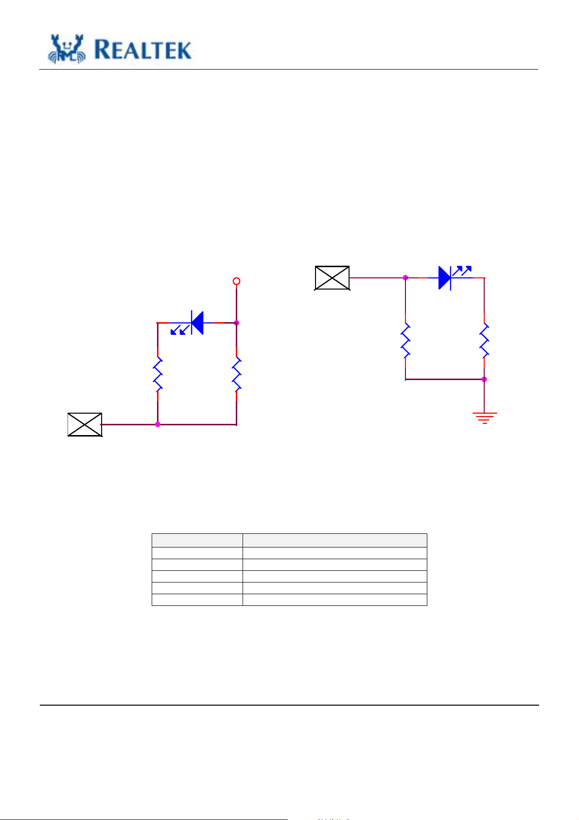
In order to reduce the pin count on the RTL8201CP, the LED pins are duplexed with the PHY address
pins. Because the PHYAD strap options share the LED output pins, the external combinations required
for strapping and LED usage must be considered in order to avoid contention. Specifically, when the LED
outputs are used to drive LEDs directly, the active state of each output driver is dependent on the logic
level sampled by the corresponding PHYAD input upon power-up/reset. For example, as Figure 5 (leftside) shows, if a given PHYAD input is resistively pulled high then the corresponding output will be
configured as an active low driver. On the right side we can see that if a given PHYAD input is resistively
pulled low then the corresponding output will be configured as an active high driver. The PHY address
configuration pins should not be connected to GND or VCC directly, but must be pulled high or low
through a resistor (ex 5.1KΩ). If no LED indications are needed, the components of the LED path
(LED+510Ω) can be removed.
VCC
PAD[0:4]/
LED[0:4]
5.1K ohm
510 ohm
PAD[0:4]/
LED[0:4]
LED
5.1K ohm
PHY Address[:] = Logical 1 PHY Address[:] = Logical 0
LED Indication = Active low LED Indication = Active High
Figure 5. LED and PHY Address Configuration
Figure 6. LED Definitions
LED LED Definitions
LED0 Link.
LED1 Full Duplex.
LED2 10-Activity.
LED3 Fiber/100-Activity.
LED4 Collision.
LED
510 ohm
Single-Chip/Port 10/100 Fast Ethernet PHYceiver 19 Track ID: JATR-1076-21 Rev. 1.1
Page 25

RTL8201CP
Datasheet
7.6. Serial Network Interface
The RTL8201CP also supports the traditional 7-wire serial interface to operate with legacy MACs or
embedded systems. To setup for this mode of operation, pull the MII/SNIB pin low. By doing so, the
RTL8201CP will ignore the setup of the ANE and SPEED pins. In this mode, the RTL8201CP will set
the default operation to 10Mbps and half-duplex mode.
Note: The RTL8201CP also supports full-duplex mode operation if the DUPLEX pin has been pulled high.
This interface consists of a 10Mbps transmit and receive clock generated by PHY, 10Mbps transmit and
receive serial data, transmit enable, collision detect, and carry sense signals.
7.7. Pow er Down, Link Down, Power Saving, and Isolation Modes
Four types of Power Saving mode operation are supported. This section describes how to implement each
mode. The first three modes are configured through software, and the fourth through hardware.
Table 27. Power Saving Mode Pin Settings
Mode Description
Analog Off Setting bit 11 of register 17 to 1 will put the RTL8201CP into analog off state. In analog off state, the
RTL8201CP will power down all analog functions such as transmit, receive, PLL, etc. However, the
internal 25MHz crystal oscillator will not be powered down. Digital functions in this mode are still
available which allows reacquisition of analog functions
LDPS Setting bit 12 of register 17 to 1, or pulling the LDPS pin high will put the RTL8201CP into LDPS
(Link Down Power Saving) mode. In LDPS mode, the RTL8201CP will detect the link status to
decide whether or not to turn off the transmit function. If the link is off, FLP or 100Mbps
IDLE/10Mbps NLP will not be transmitted. However, some signals similar to NLP will be
transmitted. Once the receiver detects leveled signals, it will stop the signal and transmit FLP or
100Mbps IDLE/10Mbps NLP again. This can cut power used by 60%~80% when the link is down.
PWD Setting bit 11 of register 0 to 1 puts the RTL8201CP into power down mode. This is the maximum
power saving mode while the RTL8201CP is still alive. In PWD mode, the RTL8201CP will turn off
all analog/digital functions except the MDC/MDIO management interface. Therefore, if the
RTL8201CP is put into PWD mode and the MAC wants to recall the PHY, it must create the
MDC/MDIO timing by itself (this is done by software).
Isolation This mode is different from the three previous software configured power saving modes. This mode
is configured by hardware pin 43. Setting pin 43 high will isolate the RTL8201CP from the Media
Access Controller (MAC) and the MDC/MDIO management interface. In this mode, power
consumption is minimal.
7.8. Media Interface
7.8.1. 100Base-TX
100Base-TX Transmit Function
Transmit data in 4-bit nibbles (TXD[3:0]) clocked at 25MHz (TXC) is transformed into 5B symbol code
(4B/5B encoding). Scrambling, serializing, and conversion to 125MHz, and NRZ to NRZI then takes
place. After this process, the NRZI signal is passed to the MLT-3 encoder, then to the transmit line driver.
Single-Chip/Port 10/100 Fast Ethernet PHYceiver 20 Track ID: JATR-1076-21 Rev. 1.1
Page 26

RTL8201CP
Datasheet
The transmitter will first assert TXEN. Before transmitting the data pattern, it will send a /J/K/ symbol
(Start-of-frame delimiter), the data symbol, and finally a /T/R/ symbol known as the End-Of-Frame
delimiter. The 4B/5B and the scramble process can be bypassed via a PHY register setting (see Table 1,
page 4, Pin number 24). For better EMI performance, the seed of the scrambler is based on the PHY
address. In a hub/switch environment, each RTL8201CP will have different scrambler seeds and so
spread the output of the MLT-3 signals.
100Base-TX Receive Function
The received signal is compensated by the adaptive equalizer to make up for signal loss due to cable
attenuation and Inter Symbol Interference (ISI). Baseline Wander Correction monitors the process and
dynamically applies corrections to the process of signal equalization. The PLL then recovers the timing
information from the signals and from the receive clock. With this, the received signal is sampled to form
NRZI data. The next steps are the NRZI to NRZ process, unscrambling of the data, serial to parallel and
5B to 4B conversion, and passing of the 4B nibble to the MII interface.
7.8.2. 100Base-FX Fiber Mode Operation
The RTL8201CP can be configured as 100Base-FX via hardware configuration. The hardware
100Base-FX setting takes priority over NWay settings. A scrambler is not required in 100Base-FX.
100Base-FX Transmit Function
Di-bits of TXD are processed as 100Base-TX except without a scrambler before the NRZI stage. Instead
of converting to MLT-3 signals, as in 100Base-TX, the serial data stream is driven out as NRZI PECL
signals, which enter the fiber transceiver in differential-pairs form.
100Base-FX Receive Function
The signal is received through PECL receiver inputs from the fiber transceiver and directly passed to the
clock recovery circuit for data/clock recovery. The scrambler/de-scrambler is bypassed in 100Base-FX.
7.8.3. 10Base-T TX/RX
10Base-T Transmit Function
Transmit data in 4-bit nibbles (TXD[3:0]) clocked at 25MHz (TXC) is first fed to a parallel-to-serial
converter, then the 10Mbps NRZ signal is sent to a Manchester encoder. The Manchester encoder
converts the 10Mbps NRZ data into a Manchester Encoded data stream for the TP transmitter and adds a
Start of Idle pulse (SOI) at the end of the packet as specified in IEEE 802.3. Finally, the encoded data
stream is shaped by a bandlimited filter embedded in the RTL8201CP and then transmitted.
10Base-T Receive Function
In 10Base-T receive mode, the Manchester decoder in the RTL8201CP converts the Manchester encoded
data stream into NRZ data by decoding the data and stripping off the SOI pulse. Then, the serial NRZ
data stream is converted to a parallel 4-bit nibble signal (RXD[0:3]).
Single-Chip/Port 10/100 Fast Ethernet PHYceiver 21 Track ID: JATR-1076-21 Rev. 1.1
Page 27

RTL8201CP
Datasheet
7.9. Repeater Mode Operation
Setting bit 15 of register 17 to 1, or pulling the RPTR pin high, sets the RTL8201CP into repeater mode.
In repeater mode, the RTL8201CP will assert CRS high only when receiving a packet. In NIC mode, the
RTL8201CP will assert CRS high both when transmitting and receiving packets. If using the RTL8201CP
in a NIC or switch application, set to the default mode. NIC/Switch mode is the default setting and has
the RPTR pin pulled low, or bit 15 of register 17 is set to 0.
7.10. Reset, and Transmit Bias
The RTL8201CP can be reset by pulling the RESETB pin low for about 10ms, then pulling the pin high.
It can also be reset by setting bit 15 of register 0 to 1, and then setting it back to 0. Reset will clear the
registers and re-initialize them. The media interface will disconnect and restart the autonegotiation/parallel detection process.
The RTSET pin must be pulled low by a 2KΩ resister with 1% accuracy to establish an accurate transmit
bias. This will affect the signal quality of the transmit waveform. Keep its circuitry away from other clock
traces or transmit/receive paths to avoid signal interference.
7.11. 3.3V Power Supply and Voltage Conversion Circuit
The RTL8201CP is fabricated in a 0.18µm process. The core circuit needs to be powered by 1.8V,
however, the digital IO and DAC circuit need a 3.3V power supply. A regulator is embedded in the
RTL8201CP to convert 3.3V to 1.8V. As with many commercial voltage conversion devices, the 1.8V
output pin (PWFBOUT) of this circuit requires the use of an output capacitor (22uF tantalum capacitor)
as part of the device frequency compensation, and another small capacitor (0.1uF) for high frequency
noise de-coupling.
PWFBIN is fed with the 1.8V power from PWFBOUT through a ferrite bead as shown in the reference
design schematic document (available for download from www.realtek.com.tw).
Note: Do not supply 1.8V produced by any power device other than PWFBOUT and PWFBIN.
The analog and digital ground planes should be as large and intact as possible. If the ground plane is large
enough, the analog and digital grounds can be separated, which is the ideal configuration. However, if the
total ground plane is not sufficiently large, partition of the ground plane is not a good idea. In this case,
all the ground pins can be connected together to a larger single and intact ground plane.
7.12. Far End Fault Indication
The MII Reg.1.4 (Remote Fault) is the Far End Fault Indication (FEFI) bit when 100FX mode is enabled
and indicates when a FEFI has been detected. FEFI is an alternative in-band signaling method which is
composed of 84 consecutive ‘1’s followed by one ‘0’. When the RTL8201CP detects this pattern three
times, Reg.1.4 is set, which means the transmit path (the Remote side’s receive path) has a problem. On
the other hand, if an incoming signal fails to cause a ‘link OK’, the RTL8201CP will start sending this
pattern, which in turn causes the remote side to detect a Far-End-Fault. This means that the receive path
has a problem from the point of view of the RTL8201CP. The FEFI mechanism is used only in 100BaseFX mode.
Single-Chip/Port 10/100 Fast Ethernet PHYceiver 22 Track ID: JATR-1076-21 Rev. 1.1
Page 28
RTL8201CP
8. Characteristics
8.1. DC Characteristics
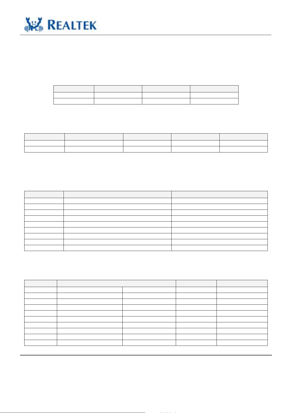
8.1.1. Absolute Maximum Ratings
Table 28. Absolute Maximum Ratings
Item Minimum Typical Maximum
Supply Voltage. 3.0V 3.3V 3.6V
Storage Temp.
-55°C
8.1.2. Operating Conditions
Table 29. Operating Conditions
Item Condition Minimum Typical Maximum
Vcc 3.3V 3.3V Supply voltage. 3.0V 3.3V 3.6V
TA Operating Temperature.
0°C
125°C
70°C
Datasheet
8.1.3. Power Dissipation
Test condition: VCC=3.3V
Table 30. Power Dissipation
Symbol Condition Total Current Consumption
P
Link down power saving mode. TBD
LDPS
P
Analog off mode. TBD
AnaOff
P
Power down mode. TBD
PWD
P
Isolate mode. TBD
Isolate
P
100Base full duplex. TBD
100F
P
10Base-T full duplex. TBD
10F
P
10Base-T transmit. TBD
10TX
P
10Base-T receive. TBD
10RX
P
10Base-T idle. TBD
10IDLE
8.1.4. Input Voltage: Vcc
Table 31. Input Voltage: Vcc
Symbol Condition Minimum Maximum
TTL VIH Input High Vol. 0.5*Vcc Vcc +0.5V
TTL VIL Input Low Vol. -0.5V 0.3*Vcc
TTL VOH Output High Vol. IOH=-8mA 0.9*Vcc Vcc
TTL VOL Output Low Vol. IOL=8mA 0.1*Vcc
TTL IOZ Tri-state Leakage. Vout=Vcc or GND -10uA 10uA
IIN Input Current. Vin=Vcc or GND -1.0uA 1.0uA
PECL VIH PECL Input High Vol. Vdd -1.16V Vdd -0.88V
PECL VIL PECL Input Low Vol. Vdd -1.81V Vdd -1.47V
PECL VOH PECL Output High Vol. Vdd -1.02V
PECL VOL PECL Output Low Vol. Vdd -1.62V
Single-Chip/Port 10/100 Fast Ethernet PHYceiver 23 Track ID: JATR-1076-21 Rev. 1.1
Page 29
RTL8201CP
8.2. AC Characteristics
8.2.1. MII Tr ansmission Cycle Tim ing
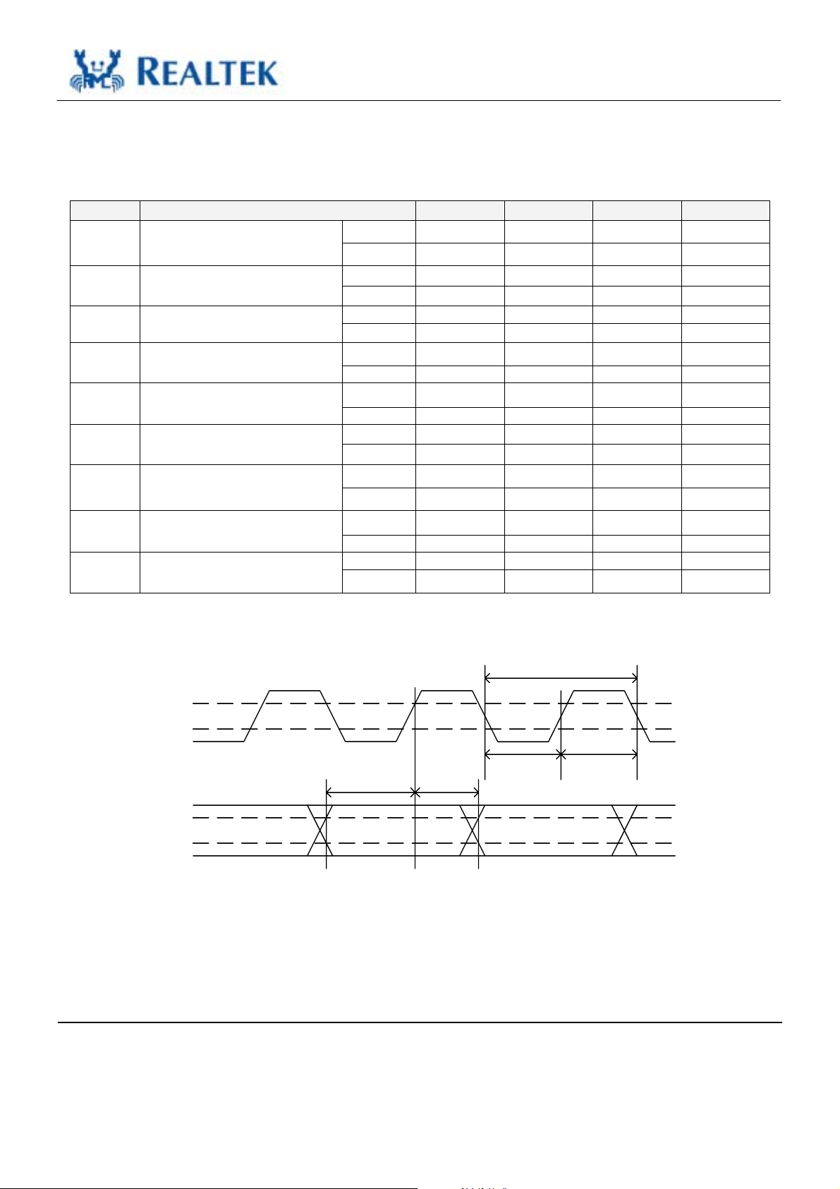
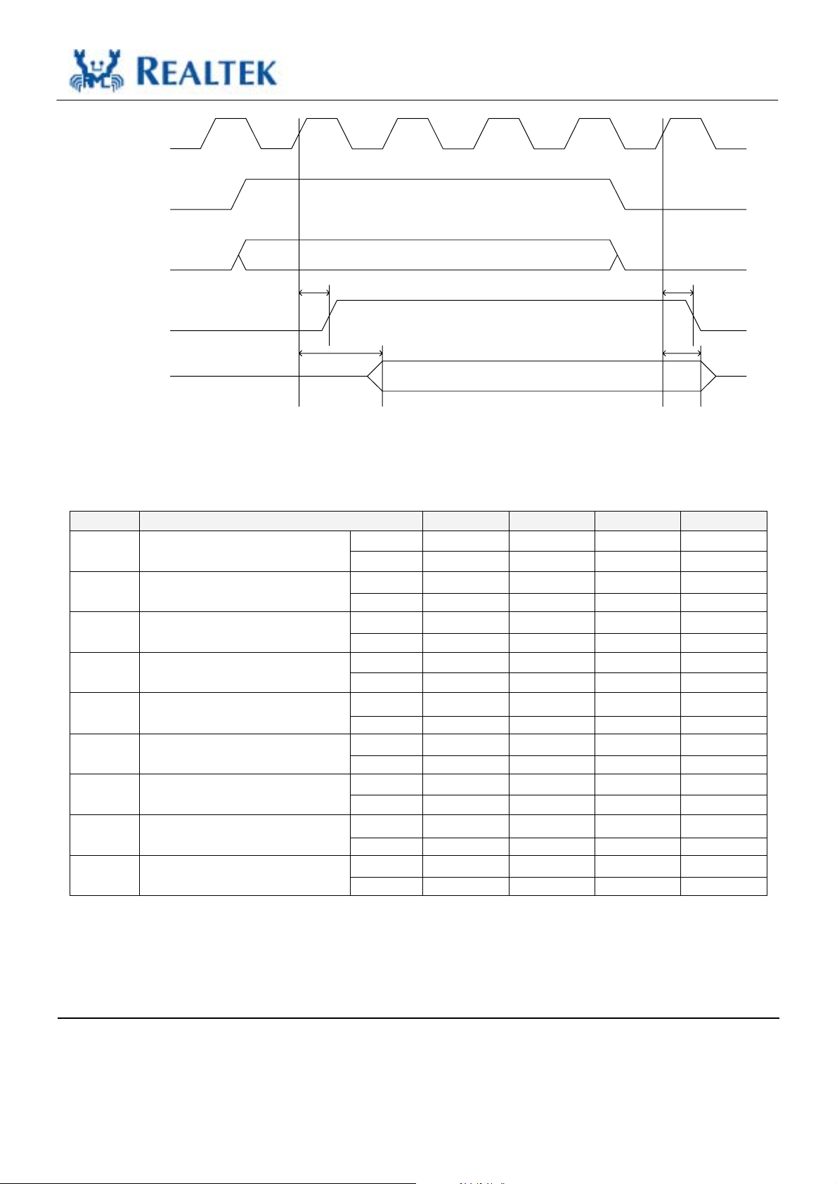
Table 32. MII Transmission Cycle Timing
Symbol Description Minimum Typical Maximum Unit
100Mbps 14 20 26 ns t1 TXCLK high pulse width.
10Mbps 140 200 260 ns
100Mbps 14 20 26 ns t2 TXCLK low pulse width.
10Mbps 140 200 260 ns
100Mbps 40 ns t3 TXCLK period.
10Mbps 400 ns
100Mbps 10 24 ns t4 TXEN, TXD[0:3] setup to
TXCLK rising edge.
TXCLK rising edge.
10Mbps 5 ns
100Mbps 10 25 ns t5 TXEN, TXD[0:3] hold after
10Mbps 5 ns
100Mbps 40 ns t6 TXEN sampled to CRS high.
10Mbps 400 ns
100Mbps 160 ns t7 TXEN sampled to CRS low.
10Mbps 2000 ns
100Mbps 60 70 140 ns t8 Transmit latency.
Datasheet
10Mbps 400 ns
100Mbps 100 170 ns t9 Sampled TXEN inactive to end
of frame.
10Mbps ns
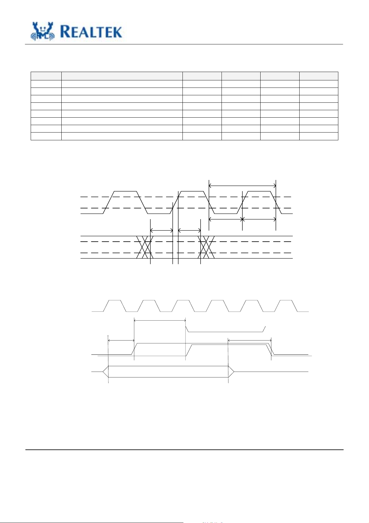
Figure 7 shows an example of a packet transfer from MAC to PHY on the MII interface.
t
3
TXCLK
t
t
4
t
5
1
t
2
TXD[0:3]
TXEN
Figure 7. MII Transmission Cycle Timing-1
V
IH(min)
V
IL(max)
V
IH(min)
V
IL(max)
Single-Chip/Port 10/100 Fast Ethernet PHYceiver 24 Track ID: JATR-1076-21 Rev. 1.1
Page 30
TXCLK
TXEN
TXD[0:3]
RTL8201CP
Datasheet
t
6
t
7
CRS
t
8
t
9
TPTX+-
Figure 8. MII Transmission Cycle Timing-2
8.2.2. MII Reception Cycle Timing
Table 33. MII Reception Cycle Timing
Symbol Description Minimum Typical Maximum Unit
100Mbps 14 20 26 ns t1 RXCLK high pulse width.
10Mbps 140 200 260 ns
100Mbps 14 20 26 ns t2 RXCLK low pulse width.
10Mbps 140 200 260 ns
100Mbps 40 ns t3 RXCLK period.
10Mbps 400 ns
100Mbps 10 ns t4 RXER, RXDV, RXD[0:3] setup
to RXCLK rising edge.
after RXCLK rising edge.
RXDV.
edge of RXDV.
10Mbps 6 ns
100Mbps 10 ns t5 RXER, RXDV, RXD[0:3] hold
10Mbps 6 ns
100Mbps 130 ns t6 Receive frame to CRS high.
10Mbps 600 ns
100Mbps 240 ns t7 End of receive frame to CRS low.
10Mbps 600 ns
100Mbps 150 ns t8 Receive frame to sampled edge of
10Mbps 3200 ns
100Mbps 120 ns t9 End of receive frame to sampled
10Mbps 800 ns
Single-Chip/Port 10/100 Fast Ethernet PHYceiver 25 Track ID: JATR-1076-21 Rev. 1.1
Page 31
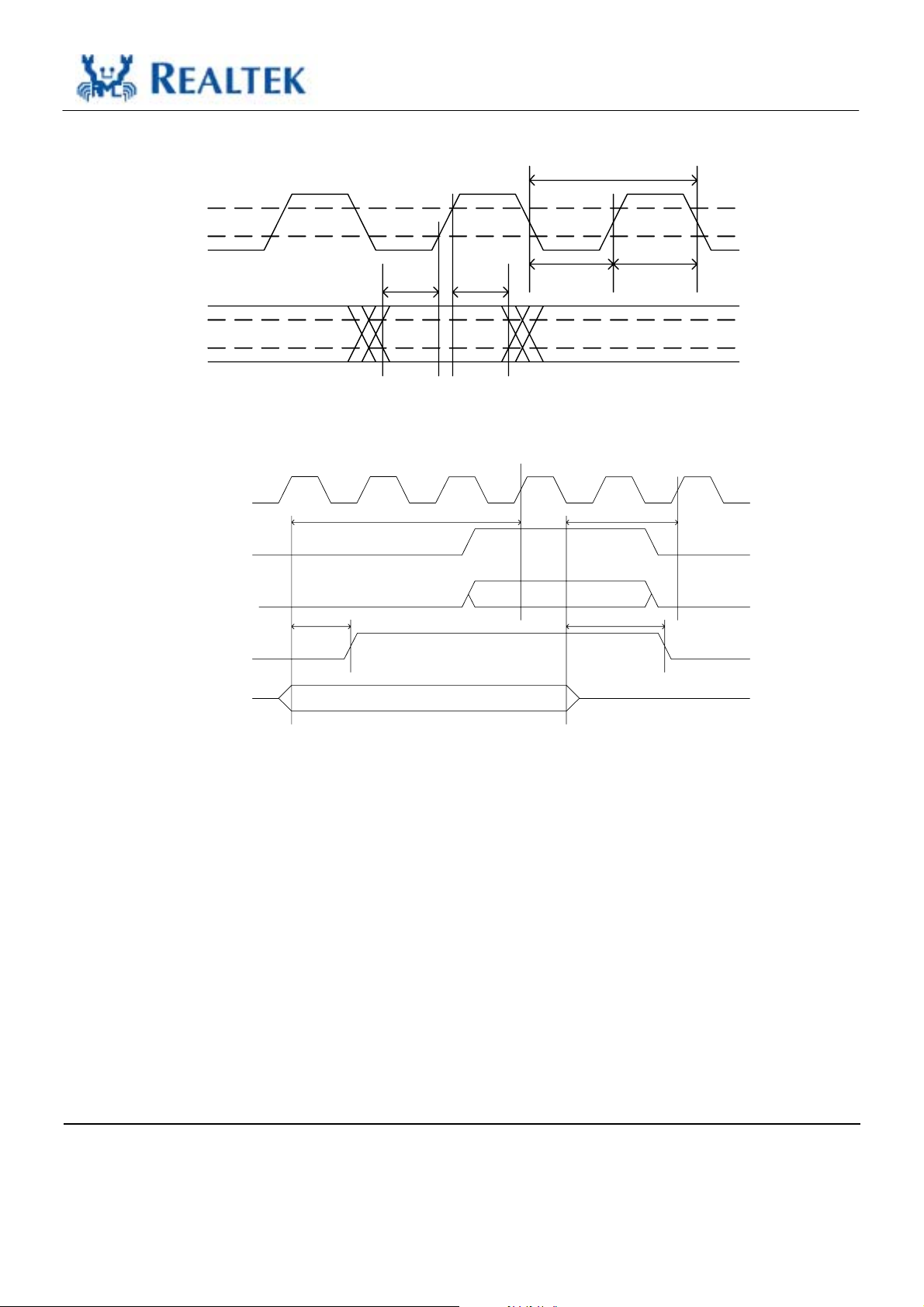
Figure 9 shows an example of a packet transfer from PHY to MAC on the MII interface.
t
3
RTL8201CP
Datasheet
RXCLK
t
4
t
5
t
1
t
2
V
IH(min)
V
IL(max)
RXD[0:3]
RXDV
RXER
Figure 9. MII Reception Cycle Timing-1
V
IH(min)
V
IL(max)
RXCLK
t
8
t
9
RXDV
RXD[0:3]
t
6
t
7
CRS
TPRX+-
Figure 10. MII Reception Cycle Timing-2
Single-Chip/Port 10/100 Fast Ethernet PHYceiver 26 Track ID: JATR-1076-21 Rev. 1.1
Page 32
8.2.3. SNI T ransmission Cycle Tim ing
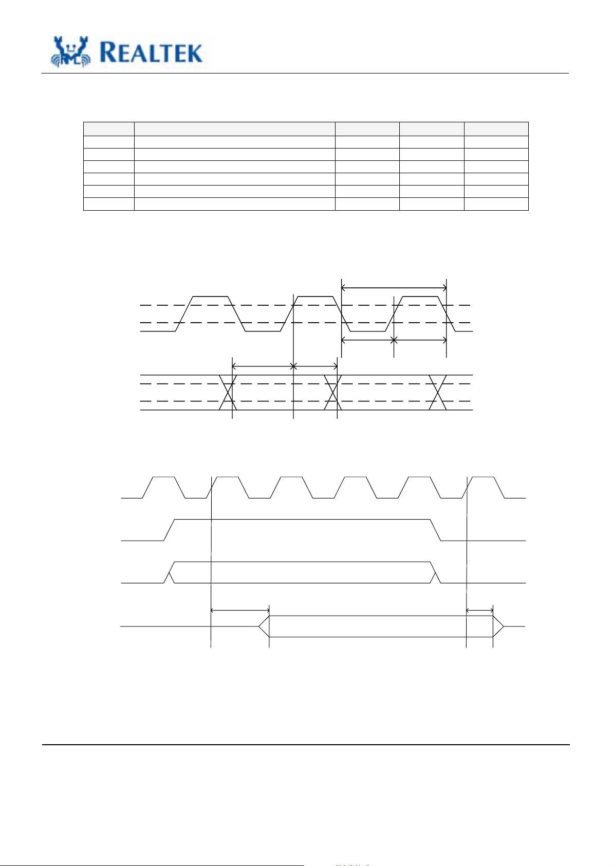
Table 34. SNI Transmission Cycle Timing
Symbol Description Minimum Maximum Unit
t1 TXCLK high pulse width 36 ns
t2 TXCLK low pulse width 36 ns
t3 TXCLK period 80 120 ns
t4 TXEN, TXD0 setup to TXCLK rising edge 20 ns
t5 TXEN, TXD0 hold after TXCLK rising edge 10 ns
t8 Transmit latency 50 ns
Figure 11 shows an example of a packet transfer from MAC to PHY on the SNI interface.
Note: SNI mode only runs at 10Mbps.
t
3
V
TXCLK
IH(min)
V
IL(max)
RTL8201CP
Datasheet
TXD0
TXEN
t
t
4
Figure 11. SNI Transmission Cycle Timing-1
t
5
1
t
2
V
IH(min)
V
IL(max)
TXCLK
TXEN
TXD0
TPTX+-
t
8
t
9
Figure 12. SNI Transmission Cycle Timing-2
Single-Chip/Port 10/100 Fast Ethernet PHYceiver 27 Track ID: JATR-1076-21 Rev. 1.1
Page 33
RTL8201CP
8.2.4. SNI Reception Cycle Timing
Table 35. SNI Reception Cycle Timing
Symbol Description Minimum Typical Maximum Unit
t1 RXCLK high pulse width. 36 ns
t2 RXCLK low pulse width. 36 ns
t3 RXCLK period. 80 120 ns
t4 RXD0 setup to RXCLK rising edge. 40 ns
t5 RXD0 hold after RXCLK rising edge. 40 ns
t6 Receive frame to CRS high. 50 ns
t7 End of receive frame to CRS low. 160 ns
t8 Decoder acquisition time. 600 1800 ns
Figure 13 shows an example of a packet transfer from PHY to MAC on the SNI interface.
Note: SNI mode only runs at 10Mbps.
t
3
V
RXCLK
t
t
4
t
5
1
t
2
IH(min)
V
IL(max)
Datasheet
RXD0
Figure 13. SNI Reception Cycle Timing-1
V
IH(min)
V
IL(max)
RXCLK
t
8
RXD0
t
6
t
7
CRS
TPRX+-
Figure 14. SNI Reception Cycle Timing-2
Single-Chip/Port 10/100 Fast Ethernet PHYceiver 28 Track ID: JATR-1076-21 Rev. 1.1
Page 34
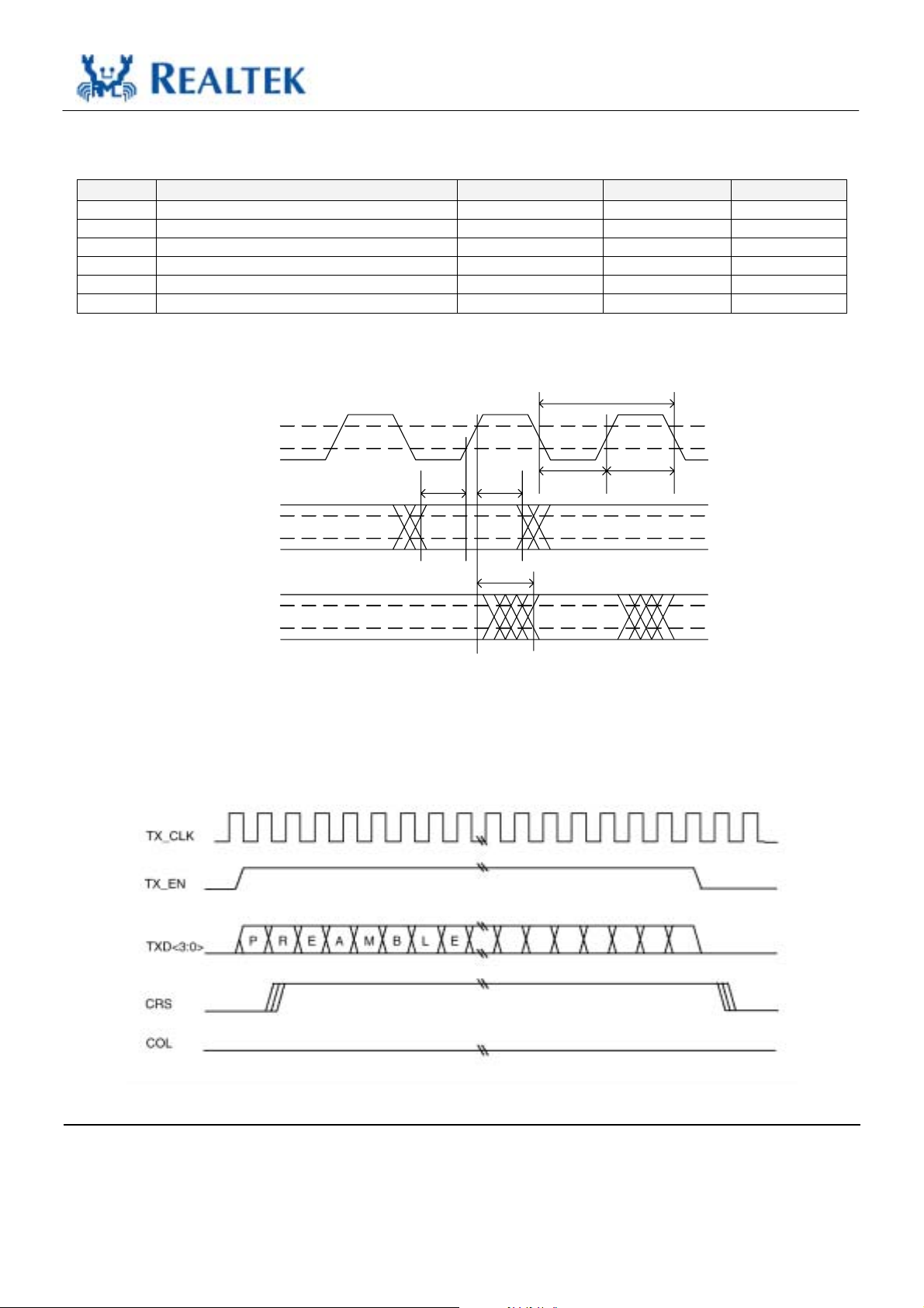
RTL8201CP
8.2.5. MDC/MDIO Timing
Table 36. MDC/MDIO Timing
Symbol Description Minimum Maximum Unit
t1 MDC high pulse width. 160 ns
t2 MDC low pulse width. 160 ns
t3 MDC period. 400 ns
t4 MDIO setup to MDC rising edge. 10 ns
t5 MDIO hold time from MDC rising edge. 10 ns
t6 MDIO valid from MDC rising edge. 0 300 ns
t
3
V
MDC
IH(min)
V
I L(max)
Datasheet
t
4
t
5
t
1
MDIO
sourced by
STA
t
6
MDIO
sourced by
RTL8201CP
Figure 15. MDC/MDIO Timing
Transmission Without Collision
Figure 16 shows an example of a packet transfer from MAC to PHY.
t
2
V
IH(min)
V
I L(max)
V
IH(min)
V
I
L(max)
Figure 16. MDC/MDIO MAC to PHY Transmission Without Collision
Single-Chip/Port 10/100 Fast Ethernet PHYceiver 29 Track ID: JATR-1076-21 Rev. 1.1
Page 35
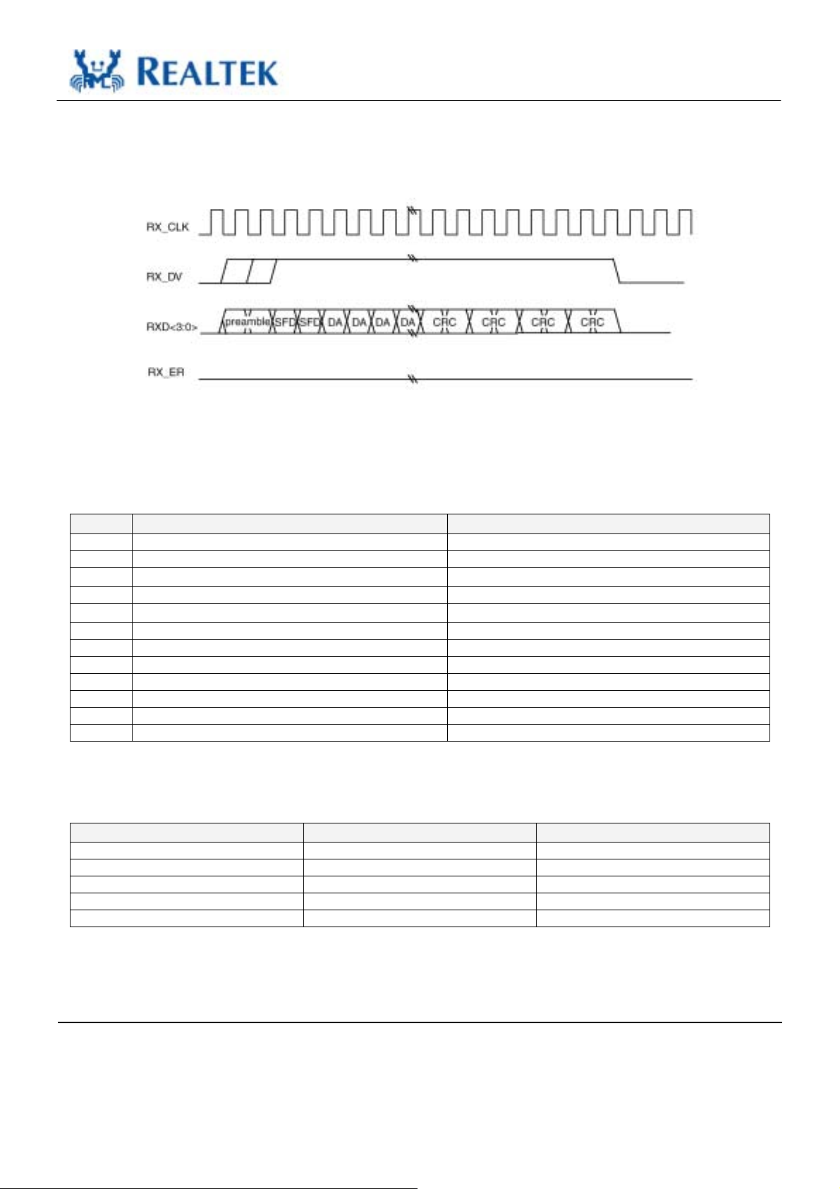
Reception Without Error
Figure 17 shows an example of a packet transfer from PHY to MAC.
Figure 17. MDC/MDIO PHY to MAC Reception Without Error
RTL8201CP
Datasheet
8.3. Crystal Characteristics
Table 37. Crystal Specifications
Item Parameter Range
1 Nominal Frequency. 25.000MHz
2 Oscillation Mode. Base wave
3
4 Temperature Characteristics. ±50 ppm
5 Operating Temperature Range.
6 Equivalent Series Resistance. 30 ohm Max.
7 Drive Level. 0.1 mV
8 Load Capacitance. 20 pF
9 Shunt Capacitance. 7 pF Max.
10 Insulation Resistance. Mega ohm Min./DC 100V
11 Test Impedance Meter. Saunders 250A
12 Aging Rate Per Year. ±0.0003%
Frequency Tolerance at 25℃.
±50 ppm
-10℃ ~ +70℃
8.4. Transformer Characteristics
Table 38. Transformer Specifications
Parameter Transmit End Receive End
Turn Ratio 1:1 CT 1:1
Inductance (min.) 350 uH @ 8mA 350 uH @ 8mA
Leakage Inductance 0.05-0.15 uH 0.05-0.15 uH
Capacitance (max) 15 pF 15 pF
DC resistance (max) 0.4 ohm 0.4 ohm
Note: To enable the Auto-Crossover Detection Function, a transformer with symmetrical TX/RX
schematics plus TX Center Tap shorted to RX Center Tap is necessary, i.e. Pulse Engineer H1245 (refer to
the suggested RTL8201CP Schematic available for download at www.realtek.com.tw).
Single-Chip/Port 10/100 Fast Ethernet PHYceiver 30 Track ID: JATR-1076-21 Rev. 1.1
Page 36
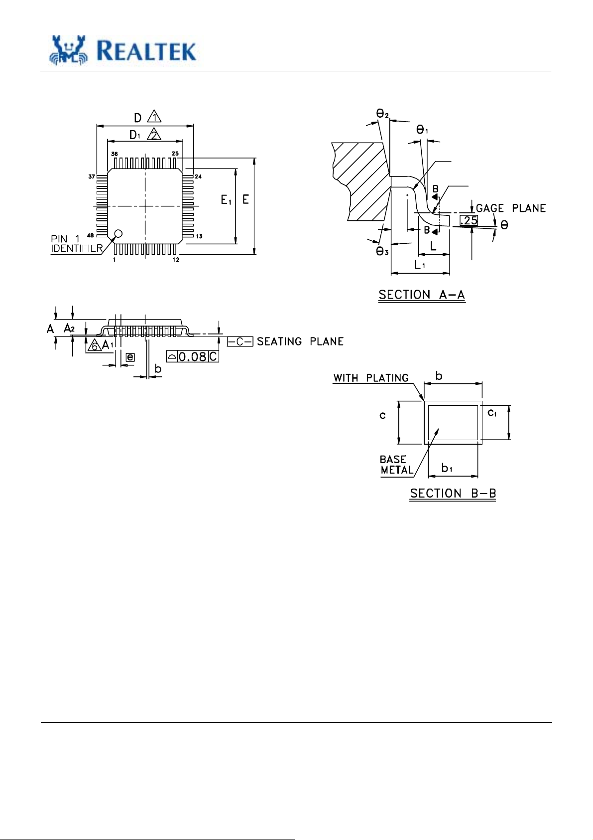
9. Mechanical Dimensions
RTL8201CP
Datasheet
See the following page for drawing related notes.
Single-Chip/Port 10/100 Fast Ethernet PHYceiver 31 Track ID: JATR-1076-21 Rev. 1.1
Page 37
RTL8201CP
Datasheet
9.1. Mechanical Dimensions Notes
Notes:
1.To be determined at seating plane -c-
2.Dimensions D1 and E1 do not include mold protrusion.
Symb
Dimension in
ol
inchs
Min Nom Max Min Nom Max 3.Dimension b does not include dambar protrusion.
A - - 0.067 - - 1.70 Dambar can not be located on the lower radius of the
A1 0.000 0.004 0.008 0.00 0.1 0.20 4.Exact shape of each corner is optional.
A2 0.051 0.055 0.059 1.30 1.40 1.50 5.These dimensions apply to the flat section of the lead
b 0.006 0.009 0.011 15 0.22 0.29 between 0.10 mm and 0.25 mm from the lead tip.
b1 0.006 0.008 0.010 0.15 0.20 0.25 6. A1 is defined as the distance from the seating plane to
c1 0.004 - 0.006 0.09 - 0.16 7.Controlling dimension: millimeter.
D 0.354 BSC 9.00 BSC 8. Reference document: JEDEC MS-026, BBC
D1 0.276 BSC 7.00 BSC
E 0.354 BSC 9.00 BSC TITLE: 48LD LQFP ( 7x7x1.4mm)
E1 0.276 BSC 7.00 BSC PACKAGE OUTLINE DRAWING, FOOTPRINT 2.0mm
e
L 0.016 0.024 0.031 0.40 0.60 0.80 DOC. NO.
L1 0.039 REF 1.00 REF VERSION 1
θ
θ1 0°
θ2 12° TYP 12° TYP
θ3 12° TYP 12° TYP
0.020 BSC 0.50 BSC LEADFRAME MATERIAL:
0° 3.5° 9° 0° 3.5° 9°
- -
Dimension in
millimeters
0°
D1 and E1 are maximum plastic body size dimensions
including mold mismatch.
foot.
the lowest point of the package body.
APPROVE
PAGE OF
- - DWG NO. SS048 - P1
CHECK
DATE
REALTEK SEMICONDUCTOR CORP.
Realtek Semiconductor Corp.
Headquarters
1F, No. 2, Industry East Road IX, Science-based
Industrial Park, Hsinchu, 300, Taiwan, R.O.C.
Tel: 886-3-5780211 Fax: 886-3-5776047
www.realtek.com.tw
Single-Chip/Port 10/100 Fast Ethernet PHYceiver 32 Track ID: JATR-1076-21 Rev. 1.1
 Loading...