

Realtek ALC662-GR, ALC662-VCO-GR, ALC662-VC1-GR, ALC662 Datasheet

ALC662 Series
(ALC662-GR, ALC662-VC0-GR, ALC662-VC1-GR)
5.1 CHANNEL HIGH DEFINITION AUDIO CODEC
DATASHEET
Rev. 1.3
03 July 2009
Track ID: JATR-1076-21
Realtek Semiconductor Corp.
No. 2, Innovation Road II, Hsinchu Science Park, Hsinchu 300, Taiwan
Tel.: +886-3-578-0211. Fax: +886-3-577-6047
www.realtek.com
ALC662 Series
COPYRIGHT
©2009 Realtek Semiconductor Corp. All rights reserved. No part of this document may be reproduced,
transmitted, transcribed, stored in a retrieval system, or translated into any language in any form or by any
means without the written permission of Realtek Semiconductor Corp.
DISCLAIMER
Realtek provides this document “as is”, without warranty of any kind. Realtek may make improvements
and/or changes in this document or in the product described in this document at any time. This document
could include technical inaccuracies or typographical errors.
TRADEMARKS
Realtek is a trademark of Realtek Semiconductor Corporation. Other names mentioned in this document
are trademarks/registered trademarks of their respective owners.
Datasheet
USING THIS DOCUMENT
This document is intended for the hardware and software engineer’s general information on the Realtek
ALC662 codec IC.
Though every effort has been made to ensure that this document is current and accurate, more
information may have become available subsequent to the production of this guide.
REVISION HISTORY
Revision Release Date Summary
1.0 2007/01/15 First release for ALC662.
1.1 2008/03/15 Added ALC662-VC (ALC662 C version) data.
Update passband ripple information in Table 82, page 64.
1.2 2008/12/02
1.3 2009/07/03 Added ALC662-VC1-GR part number information.
Correct General Description and Software Features sections. The ALC662 supports
Dolby Digital Live (Dolby Home Theater is not supported).
ALC662-VC part number corrected to ALC662-VC0-GR.
Revised Table 85, page 66.
5.1 Channel High Definition Audio Codec ii Track ID: JATR-1076-21 Rev. 1.3

ALC662 Series
Datasheet
Table of Contents
1. GENERAL DESCRIPTION..............................................................................................................................................1
2. FEATURES.........................................................................................................................................................................2
2.1. HARDWARE FEATURES ................................................................................................................................................2
2.2. SOFTWARE FEATURES..................................................................................................................................................3
2.3. ALC662-VC SERIES UPGRADED FEATURES FOR FUTURE WLP ..................................................................................4
3. SYSTEM APPLICATIONS...............................................................................................................................................4
4. BLOCK DIAGRAM...........................................................................................................................................................5
5. PIN ASSIGNMENTS .........................................................................................................................................................6
5.1. PACKAGE AND VERSION IDENTIFICATION ....................................................................................................................6
6. PIN DESCRIPTIONS.........................................................................................................................................................7
6.1. DIGITAL I/O PINS .........................................................................................................................................................7
6.2. ANALOG I/O PINS ........................................................................................................................................................7
6.3. FILTER/REFERENCE......................................................................................................................................................8
6.4. POWER/GROUND..........................................................................................................................................................8
6.5. NC (NOT CONNECTED) PINS ........................................................................................................................................8
7. HIGH DEFINITION AUDIO LINK PROTOCOL .........................................................................................................9
7.1. LINK SIGNALS ..............................................................................................................................................................9
7.1.1. Signal Definitions .................................................................................................................................................10
7.1.2. Signaling Topology...............................................................................................................................................11
7.2. FRAME COMPOSITION ................................................................................................................................................12
7.2.1. Outbound Frame – Single SDO............................................................................................................................12
7.2.2. Outbound Frame – Multiple SDOs.......................................................................................................................13
7.2.3. Inbound Frame – Single SDI................................................................................................................................14
7.2.4. Inbound Frame – Multiple SDIs...........................................................................................................................15
7.2.5. Variable Sample Rates .........................................................................................................................................15
7.3. RESET AND INITIALIZATION .......................................................................................................................................18
7.3.1. Link Reset .............................................................................................................................................................18
7.3.2. Codec Reset ..........................................................................................................................................................19
7.3.3. Codec Initialization Sequence ..............................................................................................................................20
7.4. VERB AND RESPONSE FORMAT ..................................................................................................................................20
7.4.1. Command Verb Format........................................................................................................................................20
7.4.2. Response Format..................................................................................................................................................23
7.5. POWER MANAGEMENT...............................................................................................................................................23
7.5.1. System Power State Definitions............................................................................................................................23
7.5.2. Power Controls in NID 01h..................................................................................................................................24
7.5.3. Powered Down Conditions...................................................................................................................................24
8. SUPPORTED VERBS AND PARAMETERS................................................................................................................25
8.1. VERB – GET PARAMETERS (VERB ID=F00H).............................................................................................................25
8.1.1. Parameter – Vendor ID (Verb ID=F00h, Parameter ID=00h)............................................................................25
8.1.2. Parameter – Revision ID (Verb ID=F00h, Parameter ID=02h)..........................................................................25
8.1.3. Parameter – Subordinate Node Count (Verb ID=F00h, Parameter ID=04h).....................................................26
8.1.4. Parameter – Function Group Type (Verb ID=F00h, Parameter ID=05h) ..........................................................26
8.1.5. Parameter – Audio Function Capabilities (Verb ID=F00h, Parameter ID=08h) ...............................................26
8.1.6. Parameter – Audio Widget Capabilities (Verb ID=F00h, Parameter ID=09h) ..................................................27
5.1 Channel High Definition Audio Codec iii Track ID: JATR-1076-21 Rev. 1.3

ALC662 Series
8.1.7. Parameter – Supported PCM Size, Rates (Verb ID=F00h, Parameter ID=0Ah) ................................................28
8.1.8. Parameter – Supported Stream Formats (Verb ID=F00h, Parameter ID=0Bh) .................................................29
8.1.9. Parameter – Pin Capabilities (Verb ID=F00h, Parameter ID=0Ch)..................................................................29
8.1.10. Parameter – Amplifier Capabilities (Verb ID=F00h, Input Amplifier Parameter ID=0Dh) ..........................30
8.1.11. Parameter – Amplifier Capabilities (Verb ID=F00h, Output Amplifier Parameter ID=12h) ........................30
8.1.12. Parameter – Connect List Length (Verb ID=F00h, Parameter ID=0Eh) .......................................................31
8.1.13. Parameter – Supported Power States (Verb ID=F00h, Parameter ID=0Fh) .................................................31
8.1.14. Parameter – Processing Capabilities (Verb ID=F00h, Parameter ID=10h)..................................................31
8.1.15. Parameter – GPIO Capabilities (Verb ID=F00h, Parameter ID=11h)..........................................................32
8.1.16. Parameter – Volume Knob Capabilities (Verb ID=F00h, Parameter ID=13h)..............................................32
8.2. VERB – GET CONNECTION SELECT CONTROL (VERB ID=F01H) ................................................................................33
8.3. VERB – SET CONNECTION SELECT (VERB ID=701H) .................................................................................................33
8.4. VERB – GET CONNECTION LIST ENTRY (VERB ID=F02H) .........................................................................................34
8.5. VERB – GET PROCESSING STATE (VERB ID=F03H) ...................................................................................................37
8.6. VERB – SET PROCESSING STATE (VERB ID=703H) ....................................................................................................38
8.7. VERB – GET COEFFICIENT INDEX (VERB ID=DH)......................................................................................................38
8.8. VERB – SET COEFFICIENT INDEX (VERB ID=5H) .......................................................................................................38
8.9. VERB – GET PROCESSING COEFFICIENT (VERB ID=CH) ............................................................................................39
8.10. VERB – SET PROCESSING COEFFICIENT (VERB ID=4H)..............................................................................................39
8.11. VERB – GET AMPLIFIER GAIN (VERB ID=BH) ...........................................................................................................40
8.12. VERB – SET AMPLIFIER GAIN (VERB ID=3H) ............................................................................................................43
8.13. VERB – GET CONVERTER FORMAT (VERB ID=AH)....................................................................................................44
8.14. GET CONVERTER FORMAT SUPPORT ..........................................................................................................................44
8.15. VERB – SET CONVERTER FORMAT (VERB ID=2H) .....................................................................................................45
8.16. VERB – GET POWER STATE (VERB ID=F05H)............................................................................................................46
8.17. VERB – SET POWER STATE (VERB ID=705H).............................................................................................................46
8.18. VERB – GET CONVERTER STREAM, CHANNEL (VERB ID=F06H) ...............................................................................47
8.19. VERB – SET CONVERTER STREAM, CHANNEL (VERB ID=706H) ................................................................................47
8.20. VERB – GET PIN WIDGET CONTROL (VERB ID=F07H) ..............................................................................................48
8.21. VERB – SET PIN WIDGET CONTROL (VERB ID=707H) ...............................................................................................49
8.22. VERB – GET UNSOLICITED RESPONSE CONTROL (VERB ID=F08H) ...........................................................................50
8.23. VERB – SET UNSOLICITED RESPONSE CONTROL (VERB ID=708H) ............................................................................50
8.24. VERB – GET PIN SENSE (VERB ID=F09H)..................................................................................................................51
8.25. VERB – EXECUTE PIN SENSE (VERB ID=709H)..........................................................................................................51
8.26. VERB – GET CONFIGURATION DEFAULT (VERB ID=F1CH/F1DH/F1EH/F1FH).........................................................52
8.27. VERB – SET CONFIGURATION DEFAULT BYTES 0, 1, 2, 3 (VERB ID=71CH/71DH/71EH/71FH FOR BYTES 0, 1, 2, 3) 52
8.28. VERB – GET BEEP GENERATOR (VERB ID=F0AH) ...................................................................................................53
8.29. VERB – SET BEEP GENERATOR (VERB ID=70AH)....................................................................................................53
8.30. VERB – GET GPIO DATA (VERB ID= F15H) ..............................................................................................................54
8.31. VERB – SET GPIO DATA (VERB ID= 715H)...............................................................................................................54
8.32. VERB – GET GPIO ENABLE MASK (VERB ID=F16H).................................................................................................55
8.33. VERB – SET GPIO ENABLE MASK (VERB ID=716H) .................................................................................................55
8.34. VERB – GET GPIO DIRECTION (VERB ID=F17H).......................................................................................................56
8.35. VERB – SET GPIO DIRECTION (VERB ID=717H) .......................................................................................................56
8.36. VERB – GET GPIO UNSOLICITED RESPONSE ENABLE MASK (VERB ID=F19H) .........................................................57
8.37. VERB – SET GPIO UNSOLICITED RESPONSE ENABLE MASK (VERB ID=719H)..........................................................57
8.38. VERB – GET DIGITAL CONVERTER CONTROL 1 & CONTROL 2 (VERB ID= F0DH, F0EH)..........................................58
8.39. VERB – SET DIGITAL CONVERTER CONTROL 1 & CONTROL 2 (VERB ID=70DH, 70EH)............................................59
8.40. VERB – GET SUBSYSTEM ID [31:0] (VERB ID=F20H/F21H/D22H/F23H) ..................................................................60
8.41. VERB – SET SUBSYSTEM ID [31:0] (VERB ID=723H FOR [31:24], 722H FOR [23:16], 721H FOR [15:8], 720H FOR
[7:0])..........................................................................................................................................................................60
8.42. VERB – GET EAPD CONTROL (VERB ID=F0CH).......................................................................................................61
8.43. VERB – SET EAPD CONTROL (VERB ID=70CH)........................................................................................................61
8.44. VERB – FUNCTION RESET (VERB ID=7FFH) ..............................................................................................................62
Datasheet
5.1 Channel High Definition Audio Codec iv Track ID: JATR-1076-21 Rev. 1.3

ALC662 Series
9. ELECTRICAL CHARACTERISTICS ..........................................................................................................................63
9.1. DC CHARACTERISTICS...............................................................................................................................................63
9.1.1. Absolute Maximum Ratings..................................................................................................................................63
9.1.2. Threshold Voltage ................................................................................................................................................63
9.1.3. Digital Filter Characteristics ...............................................................................................................................64
9.1.4. SPDIF Output Characteristics .............................................................................................................................64
9.2. AC CHARACTERISTICS...............................................................................................................................................65
9.2.1. Link Reset and Initialization Timing ....................................................................................................................65
9.2.2. Link Timing Parameters at the Codec..................................................................................................................66
9.2.3. SPDIF Output Timing...........................................................................................................................................67
9.2.4. Test Mode .............................................................................................................................................................67
9.3. ANALOG PERFORMANCE ............................................................................................................................................68
10. APPLICATION CIRCUITS .......................................................................................................................................69
10.1. FILTER CONNECTION .................................................................................................................................................69
10.2. ONBOARD FRONT PANEL HEADER CONNECTION AND FRONT PANEL I/O ..................................................................70
10.3. ANALOG INPUT/OUTPUT CONNECTION ......................................................................................................................71
10.4. OPTIONAL SPDIF OUTPUT.........................................................................................................................................71
11. MECHANICAL DIMENSIONS.................................................................................................................................72
11.1. MECHANICAL DIMENSIONS NOTES ............................................................................................................................73
Datasheet
12. ORDERING INFORMATION...................................................................................................................................74
5.1 Channel High Definition Audio Codec v Track ID: JATR-1076-21 Rev. 1.3

ALC662 Series
Datasheet
List of Tables
TABLE 1. DIGITAL I/O PINS.........................................................................................................................................................7
TABLE 2. ANALOG I/O PINS ........................................................................................................................................................7
TABLE 3. FILTER/REFERENCE .....................................................................................................................................................8
TABLE 4. POWER/GROUND..........................................................................................................................................................8
TABLE 5. NOT CONNECTED PINS.................................................................................................................................................8
TABLE 6. LINK RESET# ...........................................................................................................................................................10
TABLE 7. HDA SIGNAL DEFINITIONS........................................................................................................................................10
TABLE 8. DEFINED SAMPLE RATE AND TRANSMISSION RATE...................................................................................................16
TABLE 9. 48KHZ VARIABLE RATE OF DELIVERY TIMING .........................................................................................................16
TABLE 10. 44.1KHZ VARIABLE RATE OF DELIVERY TIMING ......................................................................................................17
TABLE 11. 40-BIT COMMANDS IN 4-BIT VERB FORMAT.............................................................................................................20
TABLE 12. 40-BIT COMMANDS IN 12-BIT VERB FORMAT...........................................................................................................20
TABLE 13. SUPPORTED COMMANDS ...........................................................................................................................................21
TABLE 14. SUPPORTED PARAMETERS .........................................................................................................................................22
TABLE 15. SOLICITED RESPONSE FORMAT .................................................................................................................................23
TABLE 16. UNSOLICITED RESPONSE FORMAT .............................................................................................................................23
TABLE 17. SYSTEM POWER STATE DEFINITIONS ........................................................................................................................23
TABLE 18. POWER CONTROLS IN NID 01H .................................................................................................................................24
TABLE 19. POWERED DOWN CONDITIONS ..................................................................................................................................24
TABLE 20. VERB – GET PARAMETERS (VERB ID=F00H) ............................................................................................................25
TABLE 21. PARAMETER – VENDOR ID (VERB ID=F00H, PARAMETER ID=00H).........................................................................25
TABLE 22. PARAMETER – REVISION ID (VERB ID=F00H, PARAMETER ID=02H) .......................................................................25
TABLE 23. PARAMETER – SUBORDINATE NODE COUNT (VERB ID=F00H, PARAMETER ID=04H) ..............................................26
TABLE 24. PARAMETER – FUNCTION GROUP TYPE (VERB ID=F00H, PARAMETER ID=05H)......................................................26
TABLE 25. PARAMETER – AUDIO FUNCTION CAPABILITIES (VERB ID=F00H, PARAMETER ID=08H).........................................26
TABLE 26. PARAMETER – AUDIO WIDGET CAPABILITIES (VERB ID=F00H, PARAMETER ID=09H) ............................................27
TABLE 27. PARAMETER – SUPPORTED PCM SIZE, RATES (VERB ID=F00H, PARAMETER ID=0AH)...........................................28
TABLE 28. PARAMETER – SUPPORTED STREAM FORMATS (VERB ID=F00H, PARAMETER ID=0BH) ..........................................29
TABLE 29. PARAMETER – PIN CAPABILITIES (VERB ID=F00H, PARAMETER ID=0CH)...............................................................29
TABLE 30. PARAMETER – AMPLIFIER CAPABILITIES (VERB ID=F00H, INPUT AMPLIFIER PARAMETER ID=0DH) ......................30
TABLE 31. PARAMETER – AMPLIFIER CAPABILITIES (VERB ID=F00H, OUTPUT AMPLIFIER PARAMETER ID=12H)....................30
TABLE 32. PARAMETER – CONNECT LIST LENGTH (VERB ID=F00H, PARAMETER ID=0EH)......................................................31
TABLE 33. PARAMETER – SUPPORTED POWER STATES (VERB ID=F00H, PARAMETER ID=0FH)................................................31
TABLE 34. PARAMETER – PROCESSING CAPABILITIES (VERB ID=F00H, PARAMETER ID=10H) .................................................31
TABLE 35. PARAMETER – GPIO CAPABILITIES (VERB ID=F00H, PARAMETER ID=11H)............................................................32
TABLE 36. PARAMETER – VOLUME KNOB CAPABILITIES (VERB ID=F00H, PARAMETER ID=13H) ............................................32
TABLE 37. VERB – GET CONNECTION SELECT CONTROL (VERB ID=F01H) ...............................................................................33
TABLE 38. VERB – SET CONNECTION SELECT (VERB ID=701H).................................................................................................33
TABLE 39. VERB – GET CONNECTION LIST ENTRY (VERB ID=F02H).........................................................................................34
TABLE 40. VERB – GET PROCESSING STATE (VERB ID=F03H)...................................................................................................37
TABLE 41. VERB – SET PROCESSING STATE (VERB ID=703H)....................................................................................................38
TABLE 42. VERB – GET COEFFICIENT INDEX (VERB ID=DH) .....................................................................................................38
TABLE 43. VERB – SET COEFFICIENT INDEX (VERB ID=5H).......................................................................................................38
TABLE 44. VERB – GET PROCESSING COEFFICIENT (VERB ID=CH)............................................................................................39
TABLE 45. VERB – SET PROCESSING COEFFICIENT (VERB ID=4H) .............................................................................................39
TABLE 46. VERB – GET AMPLIFIER GAIN (VERB ID=BH)...........................................................................................................40
TABLE 47. VERB – SET AMPLIFIER GAIN (VERB ID=3H)............................................................................................................43
TABLE 48. VERB – GET CONVERTER FORMAT (VERB ID=AH) ...................................................................................................44
TABLE 49. GET CONVERTER FORMAT SUPPORT .........................................................................................................................44
TABLE 50. VERB – SET CONVERTER FORMAT (VERB ID=2H).....................................................................................................45
TABLE 51. VERB – GET POWER STATE (VERB ID=F05H)...........................................................................................................46
TABLE 52. VERB – SET POWER STATE (VERB ID=705H)............................................................................................................46
5.1 Channel High Definition Audio Codec vi Track ID: JATR-1076-21 Rev. 1.3

ALC662 Series
TABLE 53. VERB – GET CONVERTER STREAM, CHANNEL (VERB ID=F06H)...............................................................................47
TABLE 54. VERB – SET CONVERTER STREAM, CHANNEL (VERB ID=706H) ...............................................................................47
TABLE 55. VERB – GET PIN WIDGET CONTROL (VERB ID=F07H)..............................................................................................48
TABLE 56. VERB – SET PIN WIDGET CONTROL (VERB ID=707H)...............................................................................................49
TABLE 57. VERB – GET UNSOLICITED RESPONSE CONTROL (VERB ID=F08H)...........................................................................50
TABLE 58. VERB – SET UNSOLICITED RESPONSE CONTROL (VERB ID=708H) ...........................................................................50
TABLE 59. VERB – GET PIN SENSE (VERB ID=F09H) .................................................................................................................51
TABLE 60. VERB – EXECUTE PIN SENSE (VERB ID=709H) .........................................................................................................51
TABLE 61. VERB – GET CONFIGURATION DEFAULT (VERB ID=F1CH/F1DH/F1EH/F1FH) ........................................................52
TABLE 62. VERB – SET CONFIGURATION DEFAULT BYTES 0, 1, 2, 3 (VERB ID=71CH/71DH/71EH/71FH FOR BYTES 0, 1, 2, 3)
..................................................................................................................................................................................52
TABLE 63. VERB – GET BEEP GENERATOR (VERB ID= F0AH)..................................................................................................53
TABLE 64. VERB – SET BEEP GENERATOR (VERB ID= 70AH)...................................................................................................53
TABLE 65. VERB – GET GPIO DATA (VERB ID= F15H) .............................................................................................................54
TABLE 66. VERB – SET GPIO DATA (VERB ID= 715H) ..............................................................................................................54
TABLE 67. VERB – GET GPIO ENABLE MASK (VERB ID= F16H) ...............................................................................................55
TABLE 68. VERB – SET GPIO ENABLE MASK (VERB ID=716H).................................................................................................55
TABLE 69. VERB – GET GPIO DIRECTION (VERB ID=F17H)......................................................................................................56
TABLE 70. VERB – SET GPIO DIRECTION (VERB ID=717H).......................................................................................................56
TABLE 71. VERB – GET GPIO UNSOLICITED RESPONSE ENABLE MASK (VERB ID=F19H) ........................................................57
TABLE 72. VERB – SET GPIO UNSOLICITED RESPONSE ENABLE MASK (VERB ID=719H) .........................................................57
TABLE 73. VERB – GET DIGITAL CONVERTER CONTROL 1 & CONTROL 2 (VERB ID= F0DH, F0EH) .........................................58
TABLE 74. VERB – SET DIGITAL CONVERTER CONTROL 1 & CONTROL 2 (VERB ID=70DH, 70EH) ...........................................59
TABLE 75. VERB – GET SUBSYSTEM ID [31:0] (VERB ID=F20H/F21H/F22H/F23H) ..................................................................60
TABLE 76. VERB – SET SUBSYSTEM ID [31:0] (VERB ID=723H FOR [31:24], 722H FOR [23:16], 721H FOR [15:8], 720H FOR
[7:0]) .........................................................................................................................................................................60
TABLE 77. VERB – GET EAPD CONTROL (VERB ID=F0CH) ......................................................................................................61
TABLE 78. VERB – SET EAPD CONTROL (VERB ID=70CH) .......................................................................................................61
TABLE 79. VERB – FUNCTION RESET (VERB ID=7FFH) .............................................................................................................62
TABLE 80. ABSOLUTE MAXIMUM RATINGS................................................................................................................................63
TABLE 81. THRESHOLD VOLTAGE ..............................................................................................................................................63
TABLE 82. DIGITAL FILTER CHARACTERISTICS ..........................................................................................................................64
TABLE 83. SPDIF OUTPUT CHARACTERISTICS ...........................................................................................................................64
TABLE 84. LINK RESET AND INITIALIZATION TIMING .................................................................................................................65
TABLE 85. LINK TIMING PARAMETERS AT THE CODEC ...............................................................................................................66
TABLE 86. SPDIF OUTPUT TIMING.............................................................................................................................................67
TABLE 87. ANALOG PERFORMANCE ...........................................................................................................................................68
TABLE 88. ORDERING INFORMATION..........................................................................................................................................74
Datasheet
5.1 Channel High Definition Audio Codec vii Track ID: JATR-1076-21 Rev. 1.3

ALC662 Series
Datasheet
List of Figures
FIGURE 1. BLOCK DIAGRAM .......................................................................................................................................................5
FIGURE 2. PIN ASSIGNMENTS ......................................................................................................................................................6
FIGURE 3. HDA LINK PROTOCOL................................................................................................................................................9
FIGURE 4. BIT TIMING...............................................................................................................................................................10
FIGURE 5. SIGNALING TOPOLOGY .............................................................................................................................................11
FIGURE 6. SDO OUTBOUND FRAME ..........................................................................................................................................12
FIGURE 7. SDO STREAM TAG IS INDICATED IN SYNC..............................................................................................................12
FIGURE 8. STRIPED STREAM ON MULTIPLE SDOS.....................................................................................................................13
FIGURE 9. SDI INBOUND STREAM .............................................................................................................................................14
FIGURE 10. SDI STREAM TAG AND DATA ..................................................................................................................................14
FIGURE 11. CODEC TRANSMITS DATA OVER MULTIPLE SDIS ....................................................................................................15
FIGURE 12. LINK RESET TIMING.................................................................................................................................................19
FIGURE 13. CODEC INITIALIZATION SEQUENCE ..........................................................................................................................20
FIGURE 14. LINK RESET AND INITIALIZATION TIMING................................................................................................................65
FIGURE 15. LINK SIGNAL TIMING ...............................................................................................................................................66
FIGURE 16. OUTPUT TIMING .......................................................................................................................................................67
FIGURE 17. FILTER CONNECTION................................................................................................................................................69
FIGURE 18. ONBOARD FRONT PANEL HEADER CONNECTION AND FRONT PANEL I/O ................................................................70
FIGURE 19. ANALOG INPUT/OUTPUT CONNECTION ....................................................................................................................71
FIGURE 20. OPTIONAL SPDIF OUTPUT .......................................................................................................................................71
5.1 Channel High Definition Audio Codec viii Track ID: JATR-1076-21 Rev. 1.3

ALC662 Series
Datasheet
1. General Description
ALC662 products are 5.1 Channel High Definition Audio Codecs designed for Windows Vista premium
desktop and mobile PCs. The ALC662, ALC662-VC0, and ALC662-VC1 (ALC662 version C series)
meet audio performance and function requirements for the latest Microsoft WLP3.10 (Windows Logo
Program).
The ALC662-VC series (ALC662-VC0 and ALC662-VC1) are upgraded versions of the ALC662 that
pass stricter WLP performance requirements (See section 2.3 ALC662-VC Series Upgraded Features for
Future WLP, page 4).
The ALC662 series feature three stereo DACs, two stereo ADCs, and legacy analog input to analog
output mixing, to provide fully integrated audio solutions for multimedia PCs and ultra mobile devices.
All analog IO (except CD-IN and PCBEEP) are input and output capable, and three headphone amplifiers
are also integrated to drive earphones on front (port-E and port-F) and rear panel (port-D).
The ALC662 series support 16/20/24-bit SPDIF output function and a sampling rate of up to 96kHz.
They offer easy connection of PCs to high quality consumer electronic products such as digital decoders
and speakers.
The ALC662 series support host audio from Intel chipsets, and also from any other HDA compatible
audio controller. With EAX/Direct Sound 3D/I3DL2 compatibility, software utilities like Karaoke mode,
environment emulation, multi-band software equalizer, 3D positional audio, and optional Dolby® Digital
Live and DTS® CONNECT™ programs, the ALC662 series provide an excellent home entertainment
package and game experience for PC users.
5.1 Channel High Definition Audio Codec 1 Track ID: JATR-1076-21 Rev. 1.3

ALC662 Series
Datasheet
2. Features
2.1.
Hardware Features
Meets premium audio requirements for Microsoft WLP 3.10 (ALC662 and ALC662-VC series)
Meets stricter performance requirements for future WLP (ALC662-VC series)
Six-channel DAC supports 16/20/24-bit PCM format for 5.1 channel audio solution
Two stereo ADCs support 16/20-bit PCM format
All DACs support independent 44.1k/48k/96kHz sample rate
All ADCs support independent 44.1k/48k/96kHz sample rate
Supports 44.1k/48k/96kHz SPDIF output
All analog jack ports are stereo input and output re-tasking
Analog differential CD input
Supports analog PCBEEP input
Integrates digital BEEP generator
Up to four channels of microphone array input are supported for AEC/BF application
Supports legacy analog input to analog output mixer
Three built-in headphone amplifiers for port-D (rear panel), port-E and port-F (front panel)
Software selectable 2.5V and 3.2V reference output for microphone bias
Software selectable boost gain (+10/+20/+30dB) for analog microphone input
Two jack detection pins: each supports detection of up to 4 jacks
Jack detection function is supported when device is in power down mode (D3)
Supports two GPIO pins (General Purpose Input Output)
Supports EAPD (External Amplifier Power Down) control for external amplifier
Supports 1.5V~3.3V scalable I/O for HD Audio link
Supports anti-pop mode when analog power AVDD is on and digital power is off
48-pin LQFP ‘Green’ package
The ALC662-VC series is fully pin compatible with the ALC662, and both are pin-to-pin compatible
with the ALC88x series and ALC262 series audio codecs
5.1 Channel High Definition Audio Codec 2 Track ID: JATR-1076-21 Rev. 1.3

2.2.
Software Features
Meets Microsoft WLP 3.10 and future WLP audio requirements
WaveRT based audio function driver and logo ready for Windows Vista
EAX™ 1.0 & 2.0 compatible
Direct Sound 3D™ compatible
I3DL2 compatible (Windows XP only)
3D Positional Audio
Emulation of 26 sound environments to enhance gaming experience
Multi-band software equalizer and software tools are provided
Voice Cancellation and Key Shifting effects
ALC662 Series
Datasheet
Dynamic range control (expander, compressor, and limiter) with adjustable parameters
Intuitive Configuration Panel (Realtek Audio Manager) for enhanced audio experience
Provides 10-foot GUI for Windows Media Center
Microphone Acoustic Echo Cancellation (AEC), Noise Suppression (NS), and Beam Forming (BF)
technology for voice application
Smart multiple streaming operation
®
Dolby
DTS
SRS® TruSurround HD (optional software feature)
Digital Live (optional software feature)
®
CONNECT™ (optional software feature)
5.1 Channel High Definition Audio Codec 3 Track ID: JATR-1076-21 Rev. 1.3

ALC662 Series
2.3.
ALC662-VC Series Upgraded Features for Future WLP
DAC and ADC keep good THD+N when tested with –1dB test signal (-3dB in WLP3.10)
DAC and ADC have less than ±0.02dB frequency response ripple (<±0.25dB in WLP3.10)
Meets performance measurement when sweeping 44.1kHz sample rate content across 20Hz to
20KHz (20Hz to 17.6KHz in WLP3.10)
The ALC662-VC1 improves anti-pop functions and reduces power consumption when the Audio
system is not in use. This is especially useful when designing equipment to meet the Energy Using
Products (EUP) directive for IT equipment
Datasheet
3. System Applications
Desktop and mobile multimedia PCs
Ultra mobile PCs
5.1 Channel High Definition Audio Codec 4 Track ID: JATR-1076-21 Rev. 1.3
4. Block Diagram
ALC662 Series
Datasheet
1Dh
1Ch
I/O
M
Surr
LINE1(Port-C)
Front
19h
I/O
M
CLfe
18h
MIC2(Port-F)
A
MIC1(Port-B)
I/O
1Eh
S/PDIF-OUT
:Output w/ Amplifier
A
O
M
CLfe
Boost
Boost
16h
CEN/LFE(Port-G)
15h
I/O
M
CLfe
14h
SURR(Port-A)
I/O
M
Surr
FRONT(Port-D)
A
BEEP-IN
CD-IN
I/O
M
Front
LINE2(Port-E)
1Bh
1Ah
A
I/O
M
Boost
CLfe
Front
BEEP Gen
0/10/20/30dB boost
Sample Rate: 44.1K, 48K, 96K
Digital Converter
M
M
M
M
S/PDIF-OUT
VOLMVOLMVOLMVOL
VOL
VOL
Surr DAC
0Dh
Front DAC
-34.5~+12dB (1.5dB/Step)
0Ch
CLfe DAC
0Eh
VOLMVOL M
0Bh
VOL
M
M
M
22h
M
M
M
MMM
M
M
M
23h
M
MMM
M
06h
M
M
M
M
M
M
M
M
M
M
M
VOLSRC
DAC
DAC
DAC
04h
SRC VOL
DAC PCM-3
03h
SRC VOL
DAC PCM-2
02h
DAC PCM-1
Sample Rate: 44.1K, 48K, 96K
VOL: -64~0dB (1.0dB/Step)
HDA I/F
1
Sample Rate: 44.1K, 48K, 96K
VOL: -13.5~+33dB (1.5dB/Step)
Parameters
SRC VOLADC
09h
ADC PCM-2
SRC VOLADC
08h
ADC PCM-1
Figure 1. Block Diagram
5.1 Channel High Definition Audio Codec 5 Track ID: JATR-1076-21 Rev. 1.3
5. Pin Assignments
ALC662 Series
Datasheet
NC
AVDD2
SURR-L( PORT-A-L)
JDREF
SURR-R( PORT-A-R)
AVSS2
CENTER( PORT-G-L)
LFE( PORT-G-R)
NC
NC
EAPD
SPDIFO
FRONT-L(PORT-D-L)
FRONT-R(PORT-D-R)
363534 33
37
38
39
40
41
42
43
44
45
LLLLLLL TXXXVV
46
47
48
1
2
NC
LINE2-VREFO
Sense B
MIC1-VREFO-R
323130 29 282726 25
ALC662
3
4
6
5
7891011 12
MIC2-VREFO
NC
MIC1-VREFO-L
AVSS1
VREF
AVDD1
24
23
22
21
20
19
18
17
16
15
14
13
LINE1-R(PORT-C-R)
LINE1-L(PORT-C-L)
MIC1-R(PORT-B-R)
MIC1-L(PORT-B-L)
CD-R
CD- GND
CD-L
MIC2-R (PORT-F-R)
MIC2-L (PORT-F-L)
LINE2-R (PORT-E-R)
LINE2-L(PORT-E-L)
Sense A
DVDD
DVSS
GPIO1
GPIO0
DVSS
BITCLK
SDATA-IN
DVDD-IO
SYNC
RESET#
PCBEEP
SDATA-OUT
Figure 2. Pin Assignments
5.1.
Package and Version Identification
Green package is indicated by a ‘G’ in the location marked ‘T’ in Figure 2. The version number is shown
in the location marked ‘VV’. For example, ‘VV=C0’ indicates silicon version ‘C’ and stepping version
‘0’, which is the stepping of the ALC662-VC0.
5.1 Channel High Definition Audio Codec 6 Track ID: JATR-1076-21 Rev. 1.3
ALC662 Series
Datasheet
6. Pin Descriptions
6.1.
Digital I/O Pins
Table 1. Digital I/O Pins
Name Type Pin Description Characteristic Definition
RESET# I 11 H/W Reset Vt=0.5*DVDDIO
SYNC I 10 Sample Sync (48kHz) Vt=0.5*DVDDIO
BITCLK I 6 24MHz Bit Clock Input Vt=0.5*DVDDIO
SDATA-OUT I 5 Serial TDM Data Input Vt=0.5*DVDDIO
SDATA-IN O 8 Serial TDM Data Output In: Vt=0.5*DVDDIO;
Out: V
SPDIFO O 48 SPDIF Output
EAPD O 47 External Amplifier Power Down VOH=DVDDIO, VOL=DVSS
GPIO0 IO 2 General Purpose Input/Output 0 In: Vt=0.5*DVDD; Out: VOH=DVDD, VOL=DVSS
GPIO1 IO 3 General Purpose Input/Output 1 In: Vt=0.5*DVDD; Out: VOH=DVDD, VOL=DVSS
Total: 9 Pins
TTL output has 12mA@75Ω driving capability
=DVDDIO, VOL=DVSS
OH
6.2.
Analog I/O Pins
Table 2. Analog I/O Pins
Name Type Pin Description Characteristic Definition
LINE2-L IO 14 2nd Line Input Left Channel Analog input/output. Default is input (JACK-E-L)
LINE2-R IO 15 2nd Line Input Right Channel Analog input/output. Default is input (JACK-E-R)
MIC2-L IO 16
MIC2-R IO 17
CD-L I 18 CD Input Left Channel Analog input. 1.6Vrms of full-scale input
CD-GND I 19 CD Input Reference Ground Analog input. 1.6Vrms of full-scale input
CD-R I 20 CD Input Right Channel Analog input. 1.6Vrms of full-scale input
MIC1-L IO 21
MIC1-R IO 22
LINE1-L IO 23 1st Line Input Left Channel Analog input/output. Default is input (JACK-C-L)
LINE1-R IO 24 1st Line Input Right Channel Analog input/output. Default is input (JACK-C-R)
PCBEEP I 12 External PCBEEP Input Analog input. 1.6Vrms of full-scale input
FRONT-L IO 35 Front Output Left Channel Analog output (JACK-D-L)
FRONT-R IO 36 Front Output Right Channel Analog output (JACK-D-R)
SURR-L IO 39 Surround Out Left Channel Analog output (JACK-A-L)
SURR-R IO 41 Surround Out Right Channel Analog output (JACK-A-R)
CENTER O 43 Center Output Analog output (JACK-G-L)
LFE O 44 Low Frequency Effects Output Analog output (JACK-G-R)
nd
Stereo Microphone Input Left
2
Channel
nd
Stereo Microphone Input
2
Right Channel
st
Stereo Microphone Input Left
1
Channel
st
Stereo Microphone Input
1
Right Channel
Analog input/output. Default is input (JACK-F-L)
Analog input/output. Default is input (JACK-F-R)
Analog input/output. Default is input (JACK-B-L)
Analog input/output. Default is input (JACK-B-R)
5.1 Channel High Definition Audio Codec 7 Track ID: JATR-1076-21 Rev. 1.3
ALC662 Series
Name Type Pin Description Characteristic Definition
Sense A I 13 Jack Detect Pin l Jack resistor network input 1
Sense B I 34 Jack Detect Pin 2 Jack resistor network input 2
Total: 20 Pins
6.3.
Filter/Reference
Table 3. Filter/Reference
Name Ty pe Pin Description Characteristic Definition
VREF - 27 Reference Voltage Typical 2.25V,10µf capacitor to analog ground
MIC1-VREFO-L O 28 Bias Voltage for MIC1 Jack 2.5V/3.2V reference voltage
MIC2-VREFO O 30 Bias Voltage for MIC2 Jack 2.5V/3.2V reference voltage
LINE2-VREFO O 31 Bias Voltage for LINE2 Jack 2.5V/3.2V reference voltage
MIC1-VREFO-R O 32 Bias Voltage for MIC1 Jack 2.5V/3.2V reference voltage
JDREF - 40
Total: 6 Pins
Reference Resistor for Jack
Detection
20K, 1% external resistor to analog ground
Datasheet
6.4.
Power/Ground
Table 4. Power/Ground
Name Ty pe Pin Description Characteristic Definition
AVDD1 I 25 Analog VDD Analog power for mixer and amplifier
AVSS1 I 26 Analog GND Analog ground for mixer and amplifier
AVDD2 I 38 Analog VDD Analog power for DACs and ADCs
AVSS2 I 42 Analog GND Analog ground for DACs and ADCs
DVDD I 1 Digital VDD Digital power for core
DVSS I 4 Digital GND Digital ground for core
DVDD-IO I 9 Digital VDD Digital power for HDA link (1.5V~3.3V)
DVSS I 7 Digital GND Digital ground for HDA link
Total: 8 Pins
6.5.
NC (Not Connected) Pins
Table 5. Not Connected Pins
Name Type Pin Description
NC - 29, 33, 37, 45, 46 Not Connected.
Total: 5 Pins
5.1 Channel High Definition Audio Codec 8 Track ID: JATR-1076-21 Rev. 1.3
ALC662 Series
Datasheet
7. High Definition Audio Link Protocol
7.1.
Link Signals
The High Definition Audio (HDA) Link is the digital serial interface that connects the HDA codecs to the
HDA Controller. The HDA link protocol is controller synchronous, based on a 24.0MHz BIT-CLK sent
by the HDA controller. The input and output streams, including command and PCM data, are isochronous
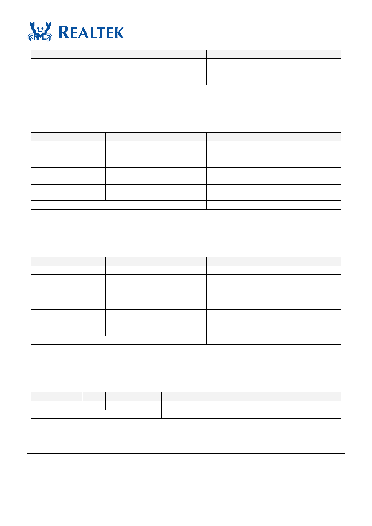
with a 48kHz frame rate. Figure 3 shows the basic concept of the HDA link protocol.
Figure 3. HDA Link Protocol
5.1 Channel High Definition Audio Codec 9 Track ID: JATR-1076-21 Rev. 1.3
7.1.1. Signal Definitions
Table 6. Link RESET#
Item Description
BCLK 24.0MHz bit clock sourced from the HDA controller and connecting to all codecs.
SYNC
SDO
SDI
RESET#
A 48kHz signal used to synchronize input and output streams on the link. It is sourced from the HDA
controller and connects to all codecs.
Serial Data Output signal driven by the HDA controller to all codecs. Commands and data streams are
carried on SDO. The data rate is double-pumped; the controller drives data onto the SDO, the codec
samples data present on SDO with respect to each edge of BCLK. The HDA controller must support at
least one SDO. To extend outbound bandwidth, multiple SDOs may be supported.
Serial Data Input signal driven by the codec. This is point-to-point serial data from the codec to the HDA
controller. The controller must support at least one SDI. Up to a maximum of 15 SDI’s can be supported.
SDI is driven by the codec at each rising edge of BCLK, and sampled by the controller at each rising
edge of BCLK. SDI can be driven by the controller to initialize the codec’s ID.
Active low reset signal. Asserted to reset the codec to default power-on state. RESET# is sourced from
the HDA controller and connects to all codecs.
ALC662 Series
Datasheet
Table 7. HDA Signal Definitions
Signal Name Source Type for Controller Description
BCLK Controller Output Global 24.0MHz Bit Clock.
SYNC Controller Output Global 48kHz Frame Sync and Outbound Tag Signal.
SDO Controller Output Serial Data Output from Controller.
SDI Codec/Controller Input/Output
RESET# Controller Output Global Active Low Reset Signal.
Serial data input from codec. Weakly pulled down by the
controller.
BCLK
SYNC
SDO
8-Bit Frame SYNC
Start of Frame
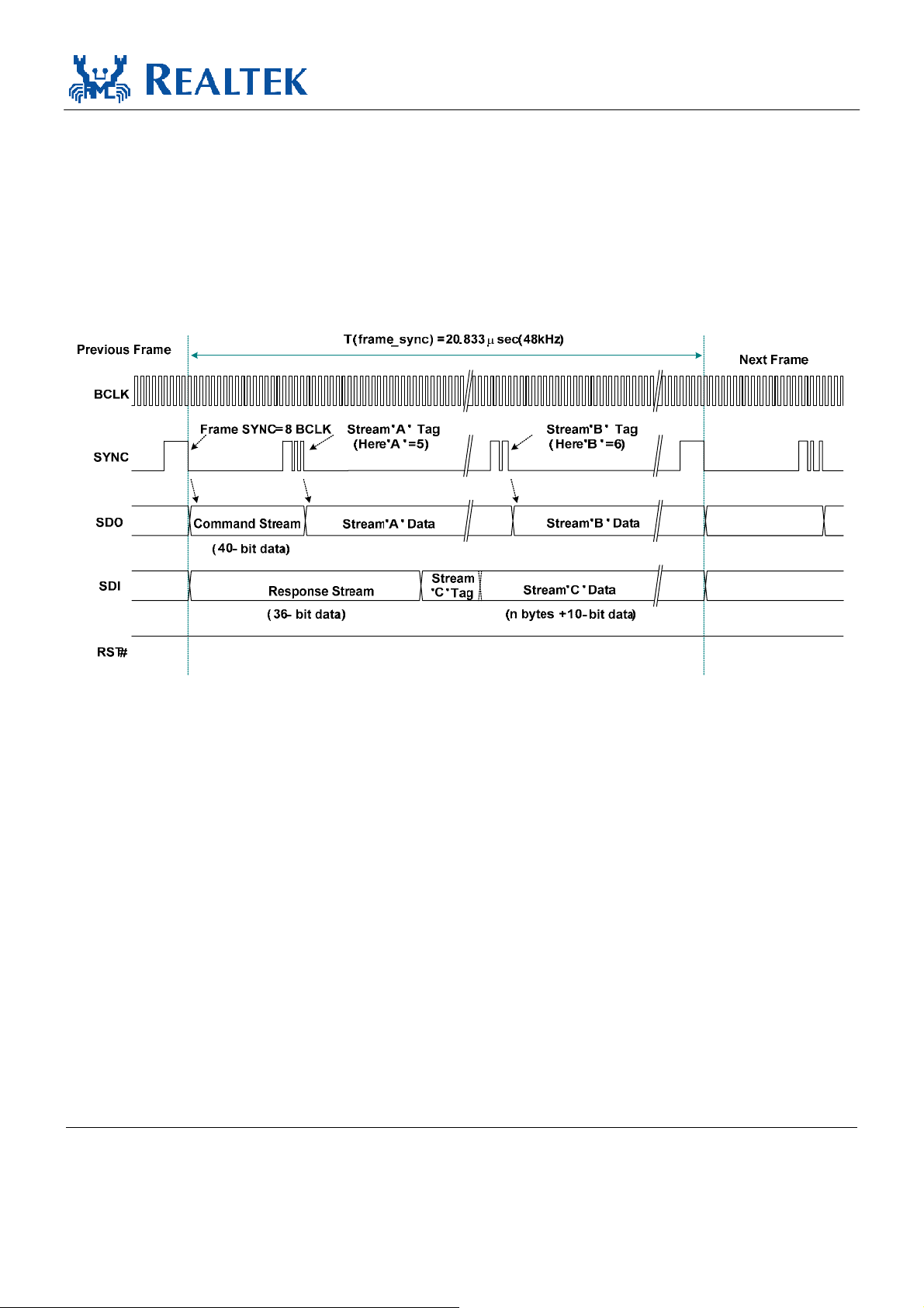
7654 0123 999 998 997 996995 994 993 992 991 990
SDI
3210 499
498
497 496 495 494
Codec samples SDO at both rising and falling edge of BCLK
Controller samples SDI at rising edge of BCLK
Figure 4. Bit Timing
5.1 Channel High Definition Audio Codec 10 Track ID: JATR-1076-21 Rev. 1.3
ALC662 Series
Datasheet
7.1.2. Signaling Topology
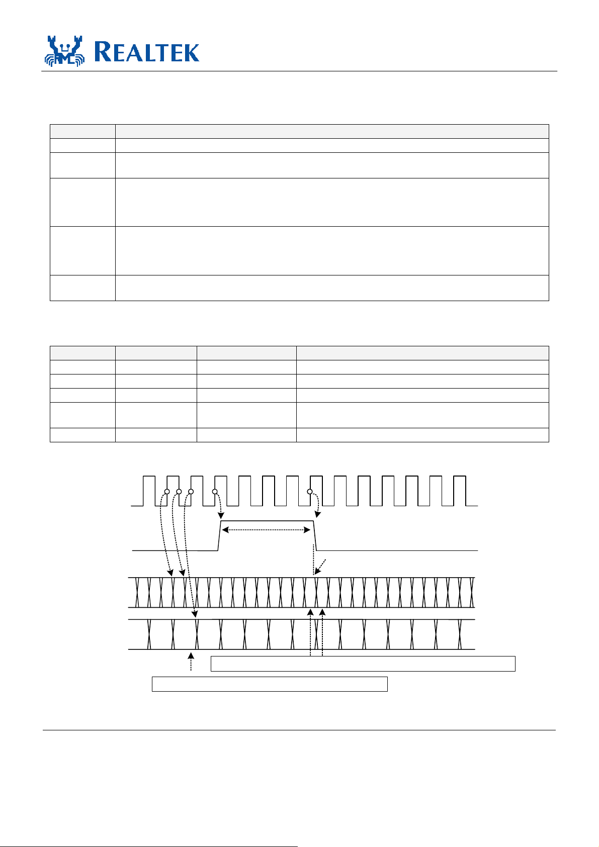
The HDA controller supports two SDOs for the outbound stream, up to 15 SDIs for the inbound stream.
RESET#, BCLK, SYNC, SDO0, and SDO1 are driven by the controller to codecs. Each codec drives its
own point-to-point SDI signal(s) to the controller.
Figure 5 shows the possible connections between the HDA controller and codecs:
• Codec 0 is a basic connection. There is one single SDO and one single SDI for normal transmission
• Codec 1 has two SDOs for doubled outbound rate, and a single SDI for normal inbound rate
• Codec 3 supports a single SDO for normal outbound rate, and two SDIs for doubled inbound rate
• Codec N has two SDOs and multiple SDIs
The multiple SDOs and multiple SDIs are used to expand the transmission rate between the controller and
codecs. Section 7.2 Frame Composition, page 12, describes the detailed outbound and inbound stream
compositions for single and multiple SDOs/SDIs.
The connections shown in Figure 5 can be implemented concurrently in an HDA system. The ALC662 is
designed to receive a single SDO stream.
SDI14
.
.
HDA
Controller
.
SDI13
SDI2
SDI1
SDI0
SDO1
SDO0
SYNC
BCLK
RST#
RST#
BCLK
SYNC
Codec 0
Single SDO
Single SDI
SDI0
SDO0
RST#
BCLK
SYNC
Codec 1
Two SDOs
Single SDI
SDO0
Figure 5. Signaling Topology
.
.
.
SDI0
SDO1
RST#
BCLK
SYNC
Codec 2
Single SDO
Two SDIs
SDI0
SDO0
SDI1
. . .
RST#
BCLK
SYNC
Codec N
Two SDOs
Multiple SDIs
SDI0
SDI2
SDO0
SDI1
SDO1
5.1 Channel High Definition Audio Codec 11 Track ID: JATR-1076-21 Rev. 1.3
ALC662 Series
Datasheet
7.2.
Frame Composition
7.2.1. Outbound Frame – Single SDO
An outbound frame is composed of one 32-bit command stream and multiple data streams. There are one
or multiple sample blocks in a data stream. Only one sample block exists in a stream if the HDA
controller delivers a 48kHz rate of samples to the codec. Multiple sample blocks in a stream means the
sample rate is a multiple of 48kHz. This means there should be 2 blocks in the same stream to carry
96kHz samples (Figure 6).
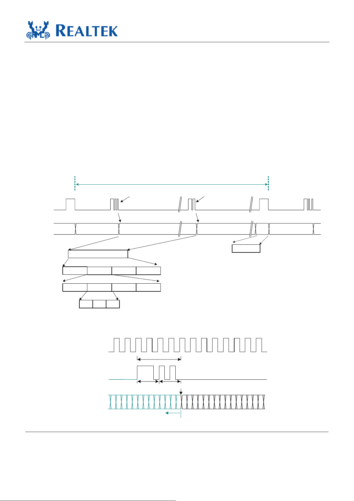
For outbound frames, the stream tag is not in SDO, but in the SYNC signal. A new data stream is started
at the end of the stream tag. The stream tag includes a 4-bit preamble and 4-bit stream ID (Figure 7).
To keep the cadence of converters bound to the same stream, samples for these converters must be placed
in the same block.
SYNC
SDO
A 48kHz Frame is composed of Command stream and multiple Data streams
Frame SYNC
Command Stream
Sample Block(s)
Block 1
Sample 1 Sample 2
msb
Block 2
...
BCLK
Stream 'A' Tag Stream 'X' Tag
(Here 'A' = 5) (Here 'X' = 6)
One or multiple blocks in a stream
..
.
..
.
msb first in a sample
lsb
Figure 6. SDO Outbound Frame
Block Y
Sample Z
Stream Tag
msb lsb
Stream 'X' DataStream 'A' Data
Null Field
For 48kHz rate, only Block1 is included
For 96kHz rate, Block1 includes (N)
includes (N+1)
Z channels of PCM sample
time of samples
th
time of samples, Block2
th
Next FramePrevious Frame
0s
Padded at the
end of Frame
0
SYNC
SDO
Preamble
(4-Bit) (4-Bit)
7654 0123
Previous Stream
110
Stream=10
Data of Stream 10
msb
Figure 7. SDO Stream Tag is Indicated in SYNC
5.1 Channel High Definition Audio Codec 12 Track ID: JATR-1076-21 Rev. 1.3
ALC662 Series
Datasheet
7.2.2. Outbound Frame – Multiple SDOs
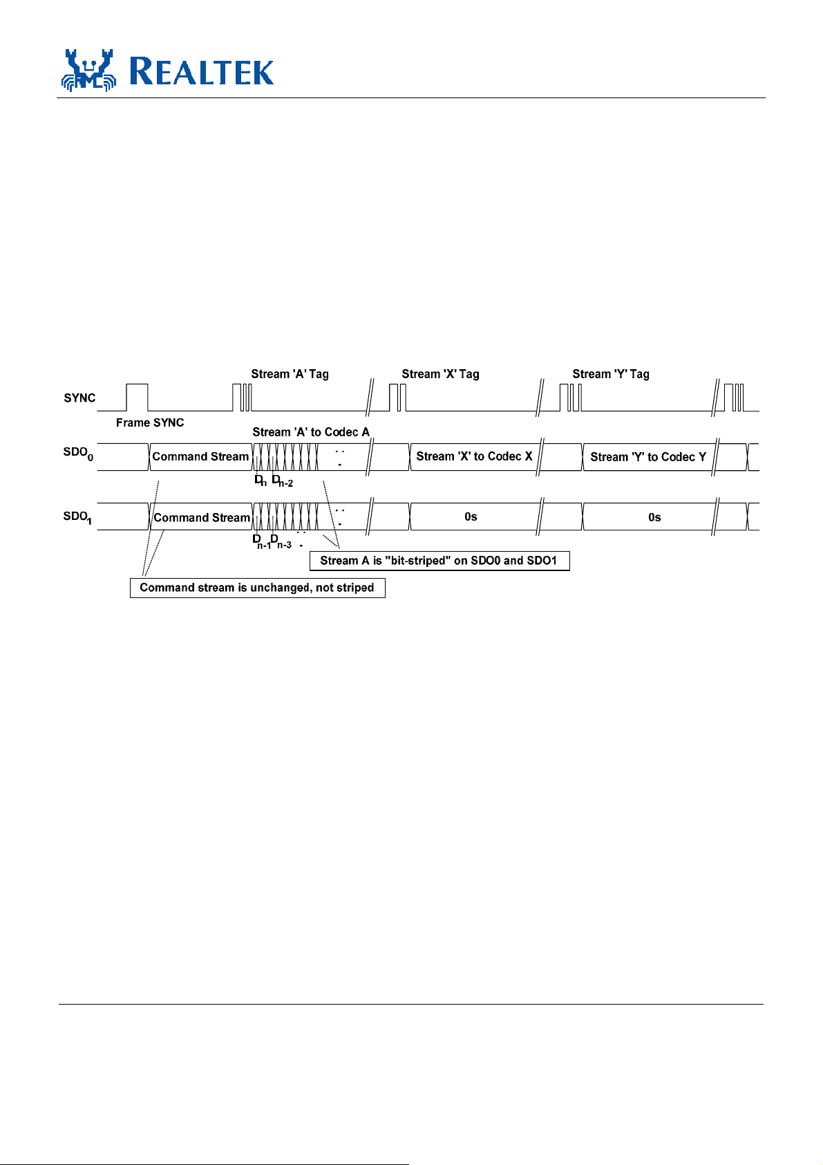
The HDA controller allows two SDO signals to be used to stripe outbound data, completing transmission
in less time to get more bandwidth. If software determines that the target codec supports multiple SDO
capability, it enables the ‘Stripe Control’ bit in the controller’s Output Stream Control Register to initiate
a specific stream (Stream ‘A’ in Figure 8) to be transmitted on multiple SDOs. In this case, the MSB of
stream data is always carried on SDO0, the second bit on SDO1 and so forth.
SDO1 is for transmitting a striped stream. The codec does not support multiple SDOs connected to
SDO0.
To ensure that all codecs can determine their corresponding stream, the command stream is not striped. It
is always transmitted on SDO0, and copied on SDO1.
Figure 8. Striped Stream on Multiple SDOs
5.1 Channel High Definition Audio Codec 13 Track ID: JATR-1076-21 Rev. 1.3
ALC662 Series
Datasheet
7.2.3. Inbound Frame – Single SDI
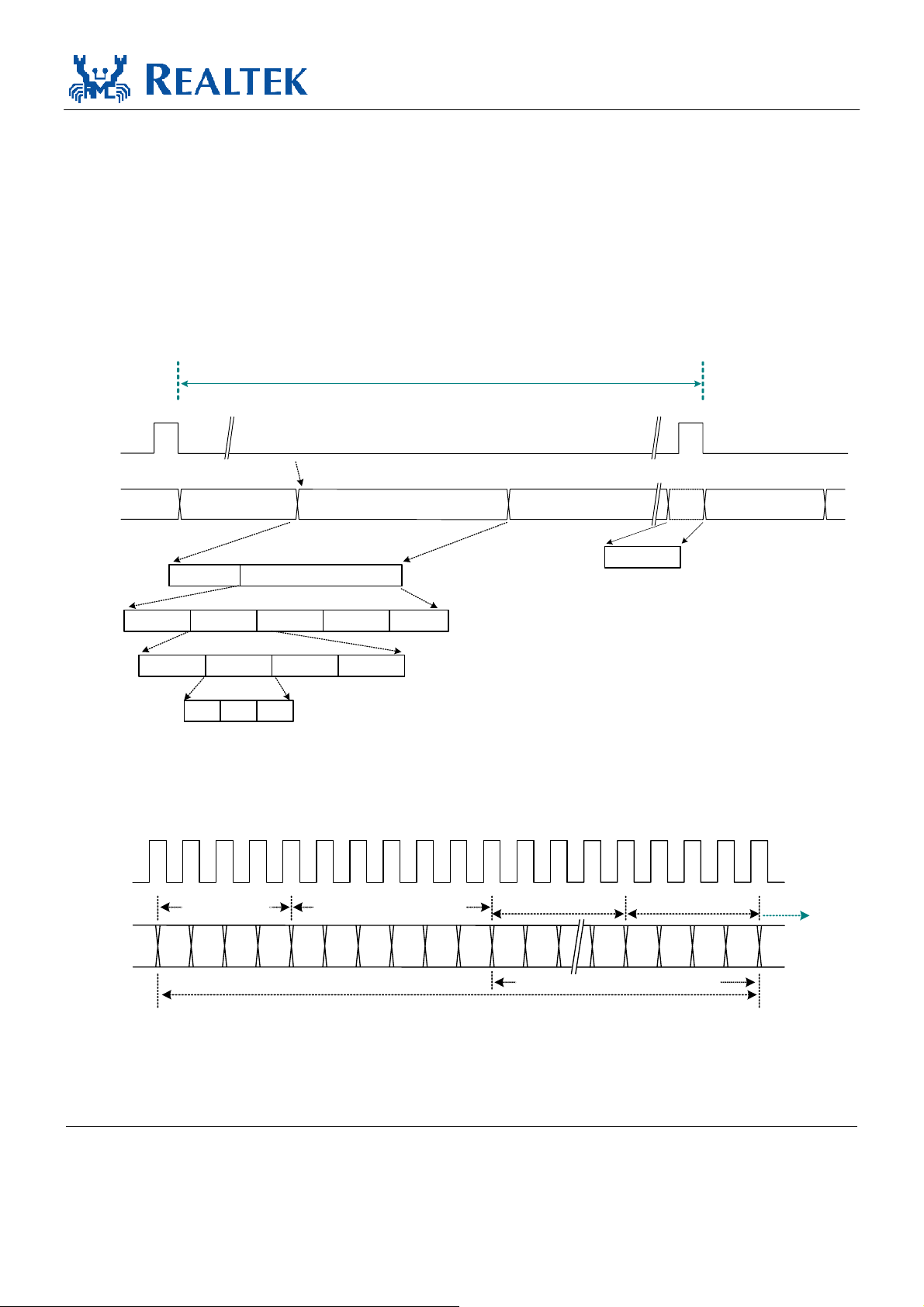
An Inbound Frame – Single SDI is composed of one 36-bit response stream and multiple data streams.
Except for the initialization sequence (turnaround and address frame), SDI is driven by the codec at each
rising edge of BCLK. The controller also samples data at the rising edge of BCLK (Figure 9).
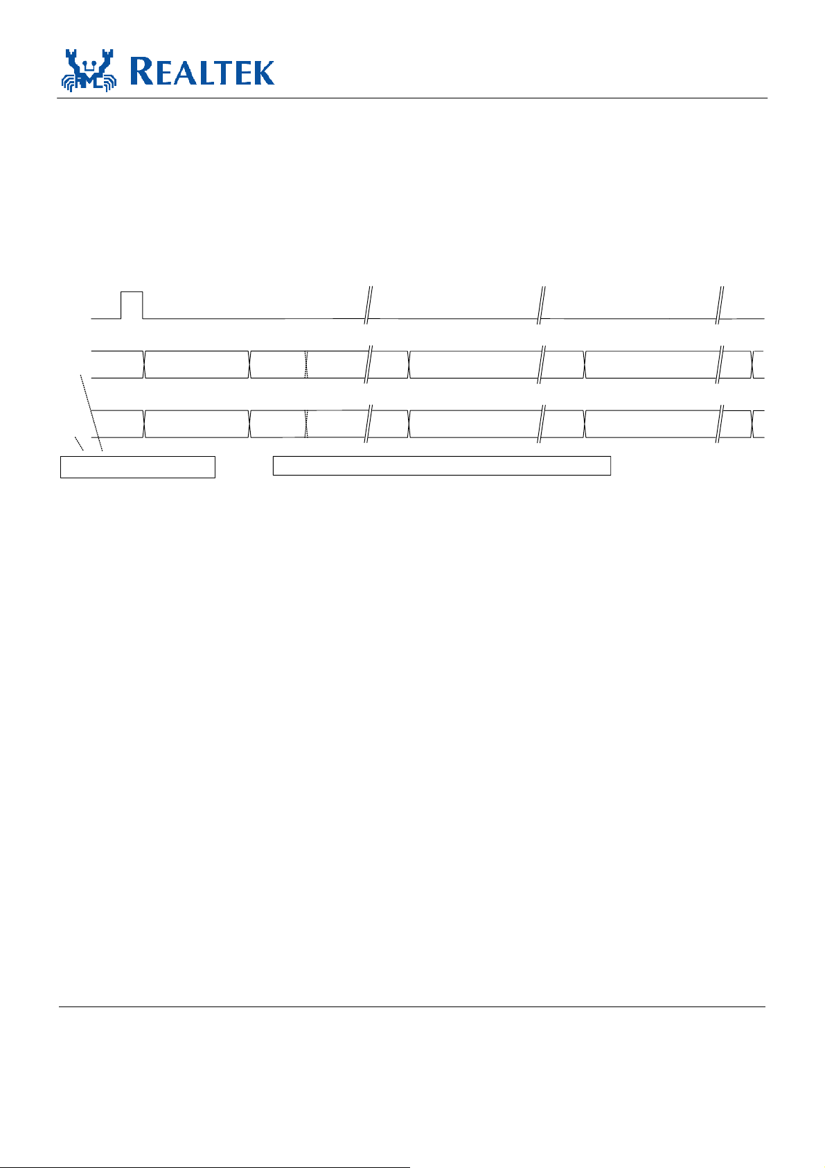
The SDI stream tag is not carried by SYNC, but included in the SDI. A complete SDI data stream
includes one 4-bit stream tag, one 6-bit data length, and n-bit sample blocks. Zeros will be padded if the
total length of the contiguous sample blocks within a given stream is not of integral byte length
(Figure 10).
SYNC
SDI
A 48kHz Frame is Composed of a Response Stream and Multiple Data streams
Frame SYNC
Response Stream
Sample Block(s)Stream Tag
Block 1
Sample 1 Sample 2 ... Sample Z
Block 2
msb ... lsb
... Block Y
msb first in a sample
Figure 9. SDI Inbound Stream
Stream 'A'
Null Pad
For 48kHz rate, only Block1 is included
For 96kHz rate, Block{1, 2} includes {(N)
Z channels of PCM sample
Stream 'X'
Null Field
Next FramePrevious Frame
0s
Padded at the end of Frame
(N+1)th} time of samples
th
BCLK
SDI
Stream Tag
B
B
8
9
Data Length in Bytes
B
B
B
B
B
B
B
7
5
6
3
4
1
2
n-Bit Sample Block
D
n-1
D
n-2
B
0
D
0
(Data Length in Bytes *8)-Bit
A Complete Stream
Figure 10. SDI Stream Tag and Data
Null Pad
00
Next Stream
00
5.1 Channel High Definition Audio Codec 14 Track ID: JATR-1076-21 Rev. 1.3
ALC662 Series
Datasheet
7.2.4. Inbound Frame – Multiple SDIs
A codec can deliver data to the controller on multiple SDIs to achieve higher bandwidth. If an inbound
stream exceeds the data transfer limits of a single SDI, the codec can divide the data onto separate SDI
signals, each of which operate independently, with different stream numbers at the same frame time. This
is similar to having multiple codecs connected to the controller. The controller samples the divided stream
into separate memory with multiple DMA descriptors, then software re-combines the divided data into a
meaningful stream.
SYNC
Frame SYNC
SDI
0
SDI
1
Codec drives SDI
Response Stream
Response Stream
and SDI
0
1
Tag A
Tag B Data B
Figure 11. Codec Transmits Data Over Multiple SDIs
Stream 'A'
Data A
Stream 'B'
Stream A, B, X, and Y are independent and have separate IDs
Stream 'X'
0s
Stream 'Y'
0s
7.2.5. Variable Sample Rates
The HDA link is designed for sample rates of 48kHz. Variable sample rates are delivered in multiple or
sub-multiple rates of 48kHz. Two sample blocks per frame result in a 96kHz delivery rate, one sample
block over two frames results in a 24kHz delivery rate. The HDA specification states that the sample rate
of the outbound stream be synchronized by the controller, not by the codec. Each stream has its own
sample rate, independent of any other stream.
The HDA controller supports 48kHz and 44.1kHz base rates. Table 8, page 16, shows the recommended
sample rates based on multiples or sub-multiples of one of the two base rates.
Rates in sub-multiples (1/n) of 48kHz are interleaving n frames containing no sample blocks. Rates in
multiples (n) of 48kHz contain n sample blocks in a frame. Table 9, page 16, shows the delivery cadence
of variable rates based on 48kHz.
The HDA link is defined to operate at a fixed 48kHz frame rate. To deliver samples in (sub) multiple
rates of 44.1kHz, an appropriate ratio between 44.1kHz and 48kHz must be maintained to avoid
frequency drift. The appropriate ratio between 44.1kHz and 48kHz is 147/160. Meaning 147 sample
blocks are transmitted every 160 frames.
5.1 Channel High Definition Audio Codec 15 Track ID: JATR-1076-21 Rev. 1.3
ALC662 Series
The cadence ‘12-11-11-12-11-11-12-11-11-12-11-11-11- (repeat)’ interleaves 13 frames containing no
sample blocks in every 160 frames. It provides a low long-term frequency drift for 44.1kHz of delivery
rate. Rates in sub-multiples (1/n) of 44.1kHz also follow this cadence and interleave n empty frames.
Rates in multiples (n) of 44.1kHz applying this cadence contain n sample blocks in the non-empty frame
AND interleave an empty frame between non-empty frames (see Table 10, page 17).
Table 8. Defined Sample Rate and Transmission Rate
(Sub) Multiple 48kHz Base 44.1kHz Base
1/6 8kHz (1 sample block every 6 frames) -
1/4 12kHz (1 sample block every 4 frames) 11.025kHz (1 sample block every 4 frames)
1/3 16kHz (1 sample block every 3 frames) -
1/2 - 22.05kHz (1 sample block every 2 frames)
2/3 32kHz (2 sample blocks every 3 frames) -
1 48kHz (1 sample block per frame) 44.1kHz (1 sample block per frame)
2 96kHz (2 sample blocks per frame) 88.2kHz (2 sample blocks per frame)
4 192kHz (4 sample blocks per frame) 176.4kHz (4 sample blocks per frame)
Datasheet
Rate Delivery Cadence Description
8kHz YNNNNN (repeat) One sample block is transmitted in every 6 frames
12kHz YNNN (repeat) One sample block is transmitted in every 4 frames
16kHz YNN (repeat) One sample block is transmitted in every 3 frames
32kHz Y2NN (repeat) One sample block is transmitted in every 6 frames
48kHz Y (repeat) One sample block is transmitted in every 6 frames
96kHz Y2 (repeat) Two sample blocks are transmitted in each frame
192kHz Y4 (repeat) Four sample blocks are transmitted in each frame
N: No sample block in a frame
Y: One sample block in a frame
Yx: X sample blocks in a frame
Table 9. 48kHz Variable Rate of Delivery Timing
5.1 Channel High Definition Audio Codec 16 Track ID: JATR-1076-21 Rev. 1.3

ALC662 Series
Table 10. 44.1kHz Variable Rate of Delivery Timing
Rate Delivery Cadence
11.025kHz
22.05kHz
44.1kHz 12-11-11-12-11-11-12-11-11-12-11-11-11- (repeat)
88.2kHz 122-112-112-122-112-112-122-112-112-122-112-112-112- (repeat)
174.4kHz 124-114-114-124-114-114-124-114-114-124-114-114-114- (repeat)
{12}{-}{11}{-}{11}{-}{12}{-}{11}{-}{11}{-}{12}{-}{11}{-}{11}{-}{12}{-}{11}{-}{11}{-}{11}{-}
(repeat)
{12}{-}{11}{-}{11}{-}{12}{-}{11}{-}{11}{-}{12}{-}{11}{-}{11}{-}{12}{-}{11}{-}{11}{-}{11}{-}
(repeat)
11.025kHz: {12}=YNNNYNNNYNNNYNNNYNNNYNNNYNNNYNNNYNNNYNNNYNNNYNNN
{11}=YNNNYNNNYNNNYNNNYNNNYNNNYNNNYNNNYNNNYNNNYNNN
{ - }=NNNN
22.050kHz: {12}=YNYNYNYNYNYNYNYNYNYNYNYN
Datasheet
{11}=YNYNYNYNYNYNYNYNYNYNYN
{ - }=NN
44.1kHz 12- =Contiguous 12 frames containing 1 sample blocks each, followed by one frame with
no sample block.
88.2kHz 122- =Contiguous 12 frames containing 2 sample blocks each, followed by one frame with
no sample block.
174.4kHz 124- =Contiguous 12 frames containing 4 sample blocks each, followed by one frame with
no sample block.
5.1 Channel High Definition Audio Codec 17 Track ID: JATR-1076-21 Rev. 1.3
 Loading...