

Page 1

VERTICAL
TO
E8
RED BIAS
<21-B>
TO
E7
GRN BIAS
E5003
E5007
TP50
RED OUTPUT
TP24
194V
TECHNICAL TRAINING
1
0
1
0
1
0
1
0
1
0
1
1
0
1
0
1
0
1
0
1
1
0
1
0
0
1
0
1
0
0
1
1
0
0
1
1
0
0
1
0
1
1
0
0
0
1
0
1
0
1
0
1
0
0
1
1
0
0
1
0
1
0
10
1
1
0
ATC010
Technical Training Manual
0
1
1
Page 2

Page 3

FOREWORD
This manual provides the service technician circuit information and troubleshooting
steps to be used while repairing the ATC010 chassis. It is intended as a training tool
and is to be used in conjunction with the ESI service information. As wi th other
training manuals, circuit description is represented with partial schematics and not
all components in a circuit are listed.
SAFETY INFORMATION CAUTION
Safety information is contained in the appropriate Service Data. All product safety
requirements must be complied with prior to returning the instrument to the
consumer. Servicers who defeat safety features or fail to perform safety checks may
be liable for any resulting damages and may expose themselves and others to
possible injury.
All integrated circuits, all surface mounted devices, and
many other semiconductors are electrostatically sensitive
and therefore require special handling techniques.
First Edition - First Printing
Copyright 2005 TTE Technology, Inc.
Trademark(s)
RCA and associated marks are trademarks of
THOMSON S.A. used under license to TTE
CORPORATION.
Printe d in U.S. A.
®
Registered Marca(s) Registrada(s)
Prepared by
Thomson, Inc for TTE Technology, Inc.
Technical Training Department, INH905
PO Box 1976
Indianapolis, Indiana 46206 U.S.A.
Page 4

Contents
FOREWORD ............................................................. 3
SAFETY INFO RMATION CAUTION ......................... 3
Overview .................................................................. 5
Standby Power Supply............................................ 6
Run Power Supply................................................. 10
System Control (All-IN-ONE Processor).............. 13
Horizontal Deflection............................................. 15
V ertical Deflection ................................................. 17
Shutdown............................................................... 18
ADM1 Module (ATSC Tuner) ................................. 20
Standby Power Supply Troubleshooting ............. 22
Run Power Supply Troubleshooting.................... 23
System Control Troubleshooting.........................25
ADM1 T roubleshooting ......................................... 26
Shutdown Troubleshooting.................................. 27
Page 5
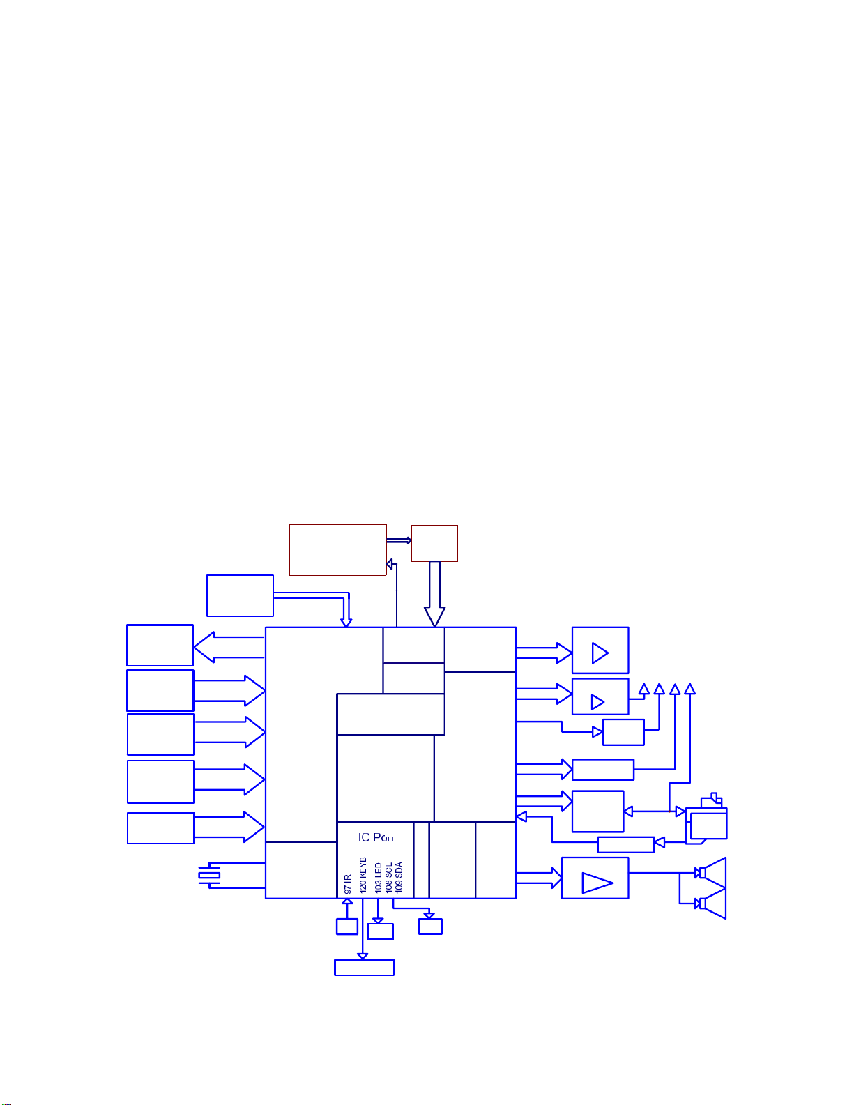
Overview
The ATC010 Training Manual covers the key circuits found i n the new ATC010
chassis. These circuits include:
· Standby Power Supply
· Run Power Supply
· System Control (ALL-IN-ONE P rocessor)
· Horizontal Deflection
· Vertical Deflection
· Shutdown Circuits
· ADM1 Module
This new chassis combines previous NTSC technology with new High Definiti on
technology. This combination allows HD programming to be received and displayed
on a standard NTSC (4:3) set. It also combines all processing and switching into a
single IC package the ALL-IN-ONE Processor.
The ALL-IN-ONE Processor is just that a single IC that handles all video switching,
audio switching, deflection processi ng, video processing, audio processing, a nd
system control functions. The only processing not performed by this IC is the ATSC
signal tuning and decoding.
P900 REAR
AV OUTPUT
P902
REAR AV IN
P901/P903
REAR AV IN
S-SHS IN
P960/P905
SIDE AV IN
SIDE SVHS IN
P904 REAR
Y Pb Pr IN
24.576MHZ
P203
from
ADM1
Y Pr Pb
36 A-OUTSL
37 A-OUTSR
48 SVO
53 AUDIO INL
54 AUDIO INR
55 CVBS2/Y2
49 AUDIO INL
50 AUDIO INR
51 CVBS4/Y4
52 C4
56 AUDIO INL
57 AUDIO INR
58 CVBS3/Y3
59 C2/C3
78 R/PrIN3
79 G/YIN3
80 B/PbIN3
PLL
10 XTAL IN
11 XTAL OUT
TUNER
NTSC
70 R/Pr
72 G/Y
71 B/Pb
AV Port
AGC
31
AGC OUT
VIF & SIF
Decoder
YUV Processor
Micro
CC V-Chip
IO Port
IR
LED
VIF / SIF
Color
P
O
W
E
R
SAW
NVM
Jungle
DSP
Stereo
IC200
RGB
RGB OUT
85,86,87
ROTATION
113
SVM 65
VDRA 23
VDRB 22
E-W 21
HD 67
FeedBack 16
AUDIO
PRE
OUT
RGB
PWM
RGB Amp
Rot Amp
VM
V-out
Pin out
H-drive
HOT
Feedback
AUDIO AMP
to YOKE
FBT
L
R
Key buttons
ATC010 System Block
Page 5
Page 6

ATSC decoding and receiving is performed on the ADM1 modul e. This module
receives and processes high definition signals and converts them to a format used
by the chassis.
Troubleshooting procedures covering key ci rcuits is also provided in this manual.
These key circuits include:
· Standby Power Supply
· Run Power Supply
· System Control
·ADM1
Each troubleshooting procedure is a step by step circuit verification process.
Knowledge of the circuit is critical to following these procedures. It is recommended
the servicing technician become familiar with the circuits before using the procedures
to troubleshoot the ATC010 chassis.
Standby Power Supply
The standby power supply in the ATC010 is operational when ever AC power is
applied to the chassis. The supply operates with an AC voltage level between 108V
to 132V. It is a switch m ode power supply that generates the +5V STB voltage from
the 120VAC input. This voltage is further regulated to a +3.3VSTBY that is used by
System Control and other circuits that require standby voltage.
The heart of the standby suppl y is IC860 switch mode controller IC. IC860 uses
voltage mode control and Pulse Width Modulation (PWM) to drive the power
transformer T860. Voltage mode control is at start up when the vol tage on pin 1
passes the start level of IC860. The PWM frequency is determined by the time it
takes for the transformer to demagnetize and an external RC network on pin 3.
Start-up
Startup of the supply occurs when AC is applied to bri dge rectifier di odes D861,
D862, D863, and D864. The AC is converted to Raw B+ (approximately +150VDC
DC) by the bridge rectifier and C860 filter. Raw B+ is the source voltage for switching
transformer T860 supplied by current limiting resistor RT860.
The switching transformer (T860) allows connection of the Raw B+ to the switch
mode controller IC through its primary winding between pin 5 and 3. Pin 3 of T860
is connected to pin 8 of IC860. IC860-8 is the Drain supply and startup for the IC.
As the Raw B+ increases on pin 8 of IC860, the IC starts to conduct through pin 6
and the current source resistor R862. As the vol tage at pin 6 of IC860 increases,
over-current is detected shutting down the IC. This releases the stored energy in the
primary of T860 to the secondary windings.
Page 6
Page 7
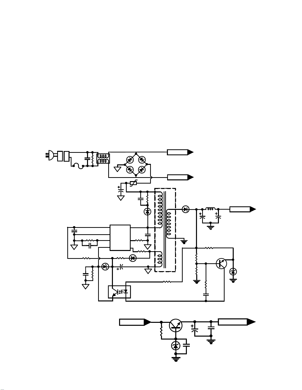
The induced voltage between secondary winding pins 1 and 2 of T860 is rectified by
D865 and filtered by C864. This voltage is used as VCC for IC860-1 and IC804-4
feedback regulation circuit. IC860 starts switching when the voltage on pin 1 passes
the VCC start level. Once this voltage is high enough to operate the IC, voltage from
pin 8 (Raw B+) is no longer used to power the IC.
IC860 operates in discontinuous conduction mode. This means that as long as there
is a pulse on the secondary of T860, the oscillat or (IC860) will not start a new p rimary
pulse. Pin 5 of IC860 m onitors the current in T860 and suppresses start of the next
cycle while there a re s t ill s e c ondary pulses from T860.
Regulation
There are two regulation circuits in the ACT010 standby power supply. D866 and
the winding from T860 pins 1 and 2 make up the secondary or fail safe regulation and
IC804 provides secondary monitoring regulation as the primary regulation. Both are
sent to IC860 pin 4 (REG input).
P802
P801
F800
C893
R849
C862
R864
C801
R801
R863
C863
T801
C861
D866
18V
IC860
1
2
3
4
4
3
R865
C864
C860
R860
D860
8
C890
7
R862
6
5
D865
1
IC804
2
RT860
R861
D861
D862
D863
D864
T860
5
3
2
1
AC-RUN
AC-RUN
R890
D868
6
L861
+5VSTB
C866
C868
10
R869
R868
R867
Q860
D869
3.3V
R891
C895
+5VSTB
R081
D080
3.9V
Q080
C083
+3.3VSTB
C082
C081
Page 7
Page 8
The primary regulation is feed back from the secondary +5VSTB source through
opto-coupler IC804. As the +5VSTB increases, current through IC804 (LE D side)
pin 1 and 2 increases. This increase is detected by the photo transistor on pins 3 and
4 causing IC804 pins 3 and 4 to conduct more. This increase in current is sent to pin
4 of IC860 causing i t to limit on time. The output voltage, in this case +5V, is
determined by Q860, D869, and voltage divider circuit R868 and R867.
Over Voltage Pr otection
The over voltage protection level is determined by D866. If the primary feed back
fails to control regulation D866 will prevent the po we r supply from reaching unsafe
levels. As the voltage increases in the secondary the voltage on the cathode of D866
also increases. Once this voltage reached the break over point of D866 (18V) D866
conducts and pin 4 of IC860 voltage increases shutting down IC860.
Over Current Protection
The current source resistor R861 determines the amount of current the power supply
can generate. As the current increases in R861, the voltage at pin 5 of IC860 starts
to increase. Once this voltage reaches the internal threshold of the IC, IC860 goes
into over current protection.
Other protections for IC860 incl ude Over Temperature and Short Circuit Winding
Protection. These protection circuits are internal of IC860 and can not be measured.
However; they both have unique circumstance that a servicer can use to determine
which shutdown it is. First is thermo shutdown, as the name implies, thermo
shutd o wn is temperatu r e r e la t ed . I f I C 8 60 g e ts t o o h ot , it will shutdo wn. With this
type of shutdown the power supply will run until the shutdown temperature is m et and
then the power supply will shutdown. Cooling down the IC will resume normal
operation of the power supply. Second, the Short Circuit Winding requires a power
on res et to c lea r. On ce activ at ed , t he s ho rt cir cu it w in din g shu td ow n will not allow
the power supply to operate until the short is removed. This results in a com pletely
dead power supply (no pulsing or oscillations).
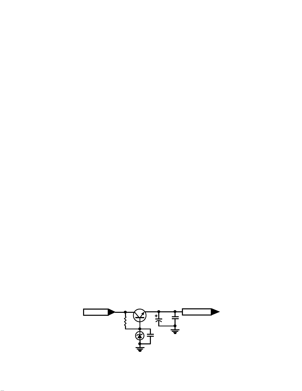
The only supply voltage generated by the standby supply is +5VSTB. This voltage
is used to run all standby circuits and is further regulated to +3.3V that is used by
system control functions. Relay K802, run supply switch, also uses the +5VSTB
Q080
+5VSTB
R081
D080
3.9V
C083
+3.3VSTB
C082
C081
Page 8
Page 9
P801
P802
AC-STBY
F800
T801
T802
D801
RT801
X800
P803
K801
P801
+5VSTB
ON/OFF
IC200
Pin99
SysCon
P802
R849
C862
R864
C801
R801
AC-STBY
F800
C801
R801
C893
R863
C863
T801
C861
D866
18V
K802
D867
IC860
1
2
3
4
4
3
Q861
R865
C864
C860
R860
D860
8
C890
7
R862
6
5
D865
1
IC804
2
RT860
R861
D861
D862
D863
D864
T860
5
3
2
1
AC-RUN
AC-RUN
R890
Run Supply
Start-UP
to R810
Run Supply
D868
6
10
R868
R867
Q880
Raw B+
to RT802
L861
R869
+12V RUN
D880
RELAY
IC200
Pin 112
SysCon
+5VSTB
C866
C868
Q860
D869
3.3V
R891
C895
Page 9
Page 10

P802
P801
ON/OFF
IC200
Pin99
AC-STBY
F800
C801
R801
AC-STBY
+5VSTB
4
1
8
C
C811
T801
IC801
4
VCC
Logic
Control
6
R815
SSFB
5
7
D813
K802
D867
OCP
1
D
S
3
T802
Q861
D812
R816
.12
2W
C815
D810
R814
R818
C812
IC802
R810
C806
D811
C813
R812
3
4
D801
R813
RT802
T803
1
9
4
7
R830
1
2
R831
RT801
18
17
10
12
16
14
15
C809
Q880
R820
L808
R822
R823
D824
D820
D822
C841
D823
D821
IC803
K801
D880
+13V
C821
L801
R835
X800
P803
+12V RUN
RELAY
R826
+12V
C838
+12V
C837
R839
R841
IC200
Pin 112
+33V
+130V
C828, C823
to
P807
Run Power Supply
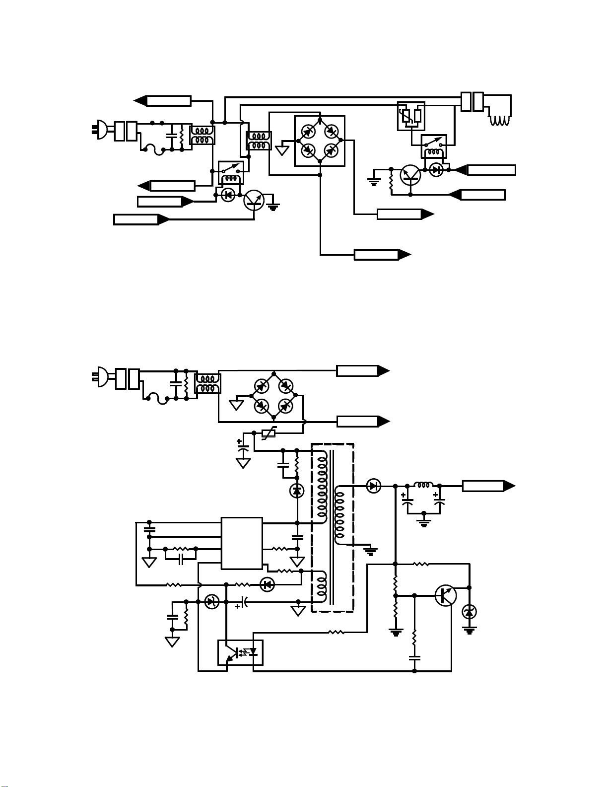
The ATC010 run power supply is a switch m ode power supply generating the +13V
source, the +33V source, Regulated B+ (+130V), and two +12V sources. It is turned
on / off by a relay switching the AC in. The heart of this switch mode pow er supply
is IC801 switch mode controller IC. IC801 is a self starting internal logic controlled
switching device that drives the transformer T803.
The run supply utilizes two shutdown circuits and feedback regulation circuit for
voltage and current control. Both shutdowns, Over-Voltage and Over Current are
monitored internal of IC801 with feedback coming from monitoring the +130V source
and the +12V source.
Start-up
Once the power on relay is energized and pin 4 of IC801 reaches the start voltage
of approximately 10.3VDC, IC801 starts to conduct through pins 1 (Drain) and 3
(Source). Raw B+ from D801 is supplied through the sw itch mode transform er T803
pins 1 and 9 to IC801 pin 1. As current increases in the source resistor R816, IC801
detects this increase at pin 5 (slow start) and starts the first cycle. The VCC from
D801 through R810 is not sufficient to operate IC801. Re-supply for VCC comes
Page 10
Page 11

Start-UP
from
D801
4
1
8
C
R810
C811
Raw B+
from D801
IC801
4
VCC
Logic
Control
OCPSSFB
6
5
7
R815
D813
1
D
S
3
R816
.12
2W
RT802
D810
C815
R814
R818
C812
C806
D811
C813
R812
IC802
3
4
R813
T803
1
9
4
7
1
2
R831
R830
C809
18
17
10
12
16
14
15
R820
L808
R822
R823
D824
D820
D822
C841
D823
D821
IC803
+13V
C821
L801
R835
+12V
C838
+12V
C837
R839
R841
+33V
R826
+130V
C828, C823
to
P807
from D810 and the secondary w inding of T803 pins 4 and 7. C814 is the filter for resupply. This re-supply voltage is also bias for the feedback opto-coupler IC802.
Feedback Regulation
There are two key components (IC802 and IC803) used for feedback regulation.
IC802 and IC803 work together to monitor the +130V source for any changes. As
the +130V increases or decrease so does the current through IC803. IC803 allows
more or less current through IC802 to occur. IC802 in turn controls the amount of
feedback being sent to IC801. IC801 uses this feedback information to control the
switching frequency.
Feedback Regulation starts with a reference voltage from the +130V source being
divided down by R835, R841, and R839. The voltage from the divider goes to IC 803
for reference. This reference voltage is 2.5V and follows the +130V as i t varies.
Increases in the reference voltage cause IC803 to conduct harder with a decrease
in reference voltage causing IC803 to conduct less.
IC803 is connected between pin 2 of IC802 (LED side) and ground. Bias for pin 1
of IC802 comes from the +12V source through R830 and R831. The voltage on pin
2 drops as the current increases in IC803 turning on the LED in IC802. The more
current IC803 draws the brighter the LED in IC802 gets. The emitted light is detected
by the photo transistor across pins 3 and 4 of IC802. The photo transistor reacts to
the amount of light being generated by the LED and conducts more current as the
light increases.
Page 11
Page 12

The photo transistor of IC802 is connected across pin 4 (VCC) and pin 6 (Feed Back)
of IC801. D813 (6.2V zener) prevents voltages lower then 6.2V from falsely tripping
the feed back and shutting down the supply.
Shutdown (Over-Voltage)
Over-voltage is detected at pin 4 (VCC) of IC801. Typically the voltage at pin 4 of
IC801 is around 9.7V during norm al operation. During Over-Voltage shutdown, the
voltage will eithe r be below 8.8V or above 10.6V. As the voltage increases at pin 4,
the internal monitor detects this increase and shuts down the IC when the voltage
exceeds +10.6VDC. Because this voltage comes from T803 pin 4, it is a good
representation of what the power supply is doing. Under voltage is also detected at
pin 4 of IC801 with the minimum requirements for operation being 8.8V. If the voltage
at pin 4 decreases below 8.8VDC, IC801 shutdowns drive.
Shutdo wn ( O ver Curre nt )
The standby supply is protected from over current conditions by shutting down IC801
when excessive current is detected. Pin 7 of IC801 is the OCP or over current protect
pin. Detection is when the voltage on pin 7 drops below zero volts. During normal
operation voltage on this pin is .46Vdc.
Start-UP
from
D801
4
1
8
C
R810
C811
Raw B+
from D801
IC801
4
VCC
Logic
Control
OCPSSFB
6
5
7
R815
D813
1
D
S
3
R816
.12
2W
RT802
D810
C815
R814
R818
C812
C806
D811
C813
R812
IC802
3
4
R813
T803
1
9
4
7
1
2
R831
R830
C809
18
17
10
12
16
14
15
R820
L808
R822
R823
D824
D820
D822
C841
D823
D821
IC803
+13V
C821
L801
R835
+12V
C838
+12V
C837
R839
R841
+33V
R826
+130V
C828, C823
to
P807
Page 12
Page 13

System Control (All-IN-ONE Processor)
The ATC010 system control is contained in an all in one processor (IC200). IC200
is a 128 pin processor capable of A/V switching and processing, Deflection
processing and drive output, Y Pr Pb processing, and CRT drive output (RGB).
IC2001 requires several voltage sources because of the different internal processing
circuits. These voltage sources come from both standby and run supplies. The
following voltages are required by IC200:
· +1.8V
· +3.3V
·+5V
·+8V
Reset for IC200 is in the form of power on reset controlled internal of the IC. When
power is applied to the set and the standby +3.3V is in the range of 2.7V to 3.3V,
IC200 will res e t . Th e re is n o e xternal indic a t io n t h a t re s e t h as o c c u r re d .
The EEPROM (IC001) is for storage of ali gnment data and customer settings is
IC001. Standard IIC bus communication is used to communi cate between IC001
and IC200. Other bus communications on the clock and data lines are between
IC200 and the ADM1 module and the Tuner (NTSC).
+5VSTB
+3.3VSTB
A (1.8V)
+5VSTB
≈
1 2 3 4 5
5 4 3 2 1
R034
Z200
L201
R047
R024
R036
L202
VDA1
VDD
D006
D005
120
5
7
9
93
96
103
97
10
11
4
R033
NTSC
Tuner
IC200
99
R049
+3.3V
to
109
108
126
100
117
118
124
SDA
SCL
98
14
3
SDA
SCL
R094
R214
R211
FPA
R027
R025
R026
R034
R093
TV STB
Q200
Q201
R029
R011
R009
R212
R213
R215
Q202
+5VSTB
IC001
4 3 2 1
5 6 7 8
Q203
+1.8V
1.5V = ON
0V = OFF
R010
SDA
SCL
IRQ
to
ADM1
+5VSTB
R216
A (1.8V)
Page 13
Page 14

A/V Processing and Switching
Another function of IC200 is to switch and process the audio and video signals. All
inputs (A/V) are switched and processed by IC200 before the signals are output from
the IC. Output from IC200 for video is RGB that is sent to the CRT video drivers.
Audio from IC200 is Right and Left signals being sent to the audio output stage.
User Interface
IC200 has two lines for user interface; pin 97 and pin120. These two lines allow the
user to control functions of the set. Pin 97 is the IR input and Pin 120 is the Key board
input. The IR signal is +5V p-p serial information stream detected by the IR sensor.
The key board input is a voltage representation of the key being pressed. A series
of resistors connected to the +3.3V source make up the voltage divider. Each key
switch is connected across a junction in the chain of resistors and ground. When a
key is pressed, the voltage drop at that junction is detected by pin 120 of IC200.
+5VSTB
+3.3VSTB
A (1.8V)
+5VSTB
≈
1 2 3 4 5
5 4 3 2 1
R034
Z200
L201
R047
R024
R036
L202
VDA1
VDD
D006
D005
120
5
7
9
93
96
103
97
10
11
4
R033
NTSC
Tuner
IC200
99
R049
+3.3V
to
109
108
126
100
117
118
124
SDA
SCL
98
14
3
SDA
SCL
R094
R214
R211
FPA
R027
R025
R026
R034
R093
TV STB
Q200
Q201
R029
R011
R009
R212
R213
R215
Q202
+5VSTB
IC001
4 3 2 1
5 6 7 8
Q203
+1.8V
1.5V = ON
0V = OFF
R010
SDA
SCL
IRQ
to
ADM1
+5VSTB
R216
A (1.8V)
Page 14
Page 15

Horizontal D eflection
The ATC010 horizontal ci rcuit consi sts of a pre-dri ver, dri ver, dri ver transformer,
HOT, E-W circuit, and IHVT. Drive for East / West correction and deflection come
from the system control processor (IC200). The purpose of horizontal is to drive the
deflection yoke and the IHVT. The IHVT generates the necessary voltages to bias
the CRT and the Vertical circuit. Other signals from the IHVT are used by the system
control for timing and control. These signals are Automatic Beam Limiter (ABL),
Sandcastle (SANCAS), and X-ray Protect (XRP).
Drive for the horizontal circui t comes from the system control (IC200-67) through
C405. This drive signal is amplified by Q403 pre-amp before being sent to the driver
Q402. Bias for Q403 is through R413 from the +12V initially and then from the +14V
after horizontal is operational. Q402 drives the horizontal driver transformer (T401)
that is directly connected to the horizontal output Q405. Bias for Q405 is through
T402 (IHVT) from the +130V run source.
As Q405 (Horizontal Output Transistor) conducts, current through T402 and the
horizontal yoke windings increases. When Q405 stops conducting, energy stored
in T402 primary is transferred to the secondaries. The secondary voltages are:
· +200V for CRT cathode
· EHT or High Voltage
·Focus
· Screen
· + / – 14V for vertical and horizontal operation
· ABL or Automatic Beam Limiter
+ 12V
+ 14V
H-OUT
E-W
D409
D411
C402
C405
D412
R413
R412
R406
C406
Q403
C407
Q402
+ 130V
R409
R410
T401
L404
+ 200V
Q405
D408
5.6V
C408
R418
R419
R420
Q407
L400
C400
D401
C414
D402
R401
D400
L403
C411
C412
C410
C413
T402
2
9
1
HORIZ -
HORIZ +
8
R424
6
10
7
3
4
SCREEN
R407
R427
R426
to Yoke
Plug P400
EHT
FOCUS
ABL
C420
D413
5.1V
D406
D405
D404
R433
R425
SANCAS
HEATER
XRP
C417
- 14V
C416
+ 14V
C415
Page 15
Page 16

The changing current in the horizontal deflection yoke windings force the beam to
move back and forth across the screen. How far (Width) across the screen the beam
travels is controlled by the E-W circuit connect to the low side of the deflection yoke.
E-W Correction
East West correction starts with drive from IC200 pin 21 going to Q407 gate. Q407
modulates the current flowing it the deflection yoke by changing the waveform
present on the low side of the yoke. Bias for Q407 comes from D402, C411 and C412
through L403 and R420.
Width is controlled by Q407s on time. The longer Q407 rem ains on, the more pulled
in the pic tur e w ill look . Sh ort er o n tim e cre ate s a w id er pict ur e. IC 200 digital data
(adjustable data) allows adjustment of the wi dth and pin correction through the
service menu. These adjustments affect the dri ve signal going to Q407. See the
electronic service data for instructions regarding how to make these adjustments.
+ 12V
+ 14V
H-OUT
E-W
D409
D411
C402
C405
D412
R413
R412
R406
C406
Q403
C407
Q402
+ 130V
R409
R410
T401
L404
+ 200V
Q405
D408
5.6V
C408
R418
R419
R420
Q407
L400
C400
D401
C414
D402
R401
D400
L403
C411
C412
C410
C413
T402
2
9
1
HORIZ -
HORIZ +
8
R424
6
10
7
3
4
SCREEN
R407
R427
R426
to Yoke
Plug P400
EHT
FOCUS
ABL
C420
D413
5.1V
D406
D405
D404
R433
R425
SANCAS
HEATER
XRP
C417
- 14V
C416
+ 14V
C415
Page 16
Page 17

V ertical Deflection
The ATC010 uses a ramp generator IC200 and deflection booster IC301 to drive the
vertical yoke windings. IC301 uses the + and – 14V to generate enough flyback
voltage for vertical deflection. Drive for IC301 comes from the system control IC200
and is labeled VDRA and VDRB. Vertical deflection is monitored by V-Loss circuit
that forces shutdown the set if vertical deflection is lost.
VCC is supplied to pin 2 from the +14V source and the -14V supplies pin 4 of IC301.
The +14V source is used through first half of the screen with 0 volts being center of
the screen. The second or bottom half is driven by the -14V source. Return or retrace
to the top comes from the flyback generator circuit between pins 3 and 6. C323 and
D309 assist with the flyback generator to create the voltage necessary to move the
beam from bottom of the screen back to top of the screen. This is known as retrace.
During retrace more voltage needs to be applied to the yoke so the beam will retu rn
to the top much quicker than when it scanned down. Because the vertical circuit uses
two supplies (-14V and +14V) and because retrace must occur in such a short time
compared to trace, a higher positive supply is needed. During trace, the negative
lead of C323 (pin 3) i s connected to the -14V suppl y internal of IC301. With the
positive lead of C323 connected to the +14V supply, there is approx imately 28 volts
across C323. At retrace, the flyback generator connects pin 3 to pin 2 applying the
+14V supply to the negative side of C323. D309 blocks current flow between C323
and the +14V supply. With the stored charge on C323 and the +14V supply on the
negative terminal, about +42 volts is supplied to pin 6. The increased voltage quickly
retraces the beam to the top of the screen.
Output from pin 5 drives the deflection yoke. The return from the yoke goes to pin
1 as feedback reference through R315 and C337.
D309
V-Loss
3
FLYBACK
GENERATOR
THERMAL
PROTECTOR
C325
C323
IC301
5
R324
R313
R321
D311
R315
C337
1
1W
P400
1
2
3
4
VDRB
VDRA
R350
+14V
-14V
R314
C308
R316
-14V
C360
62
1
+
Power Amp
-
7
4
C324
Page 17
Page 18

Drive for IC301 comes from IC200 and is applied to pins 1(non-inverting input) and
7 (inverting input). These two signals are combined in IC301 to generate the vertical
ramp needed to drive the deflection yoke. Protection from residual energy in the
vertical yoke windings is provided by R324 and D311. Also in the output circuit is
R321. R321 provides ground reference for the low side of the vertical yoke.
D309
V-Loss
C360
C323
+14V
3
FLYBACK
THERMAL
PROTECTOR
IC301
5
R313
R324
R315
C337
D311
R321
1
1W
P400
1
2
3
4
VDRB
VDRA
R350
-14V
R314
C308
R316
-14V
62
GENERATOR
1
+
Power Amp
-
7
4
C325
C324
Shutdown
The ATC010 chassis has three deflection type shutdowns Vertical, XRP, and ABL.
Each of these shutdowns com municate back to IC200 through the XRP detect pin
119. All the deflection shutdowns are detected as XRP. XRP shutdown is active low.
Vertical Shutdown
The vertical shutdown is active when loss of vertical deflection occurs. The detection
circuit for vertical shutdown consists of D300, D307, D308, C300, C307, C313, and
R300. The circuit is designed as a voltage divider between R030 and R300 that is
active only when vertical deflection is lost.
W ith verti cal defl ecti on at decoupling capaci tor C313, D307 and D308 rectify the
vertical pulse, D306 regulates the pulse and C307 filters it. With 3.9V on the anode
of D300 it is not conducting. During vertical loss, D300 is forward biased and R300
is in series with R030 creating a voltage divider, dropping the voltage on pin 119 of
IC200. This causes the set to shutdown when vertical deflection is lost.
XRP Shutdow n
The XRP circuit monitors the flyback Heater pulse for both excessive and m inimal
voltage. D406 rectifies the heater pulse from pin 10 of T402 to be used by the X RP
circuit. The rectified voltage is in the range of +10V to + 30V. A ny voltage outside
of this range will cause t h e X R P circuit to tr ip sh ut t in g do wn the se t .
Page 18
Page 19

The XRP circuit is made up of two transistors (Q280, and Q280), diodes D280, D281,
D282, and D283. A +12V source provides bias to the circuit. Q280 is used to detect
the lack of high voltage or high voltage too low. If the voltage on the base of Q280
drops below the emitter voltage of +12V, Q280 turns on and supplies Q281 base with
.7Vdc from the +12V source. Q281 turns on pulling the XRP line low making it active
and shutting down the set.
For excessive high voltage, D280 (24V zener) is used. As high voltage increases,
the voltage from D406 also increases. Once this voltage exceeds the break over
voltage of D280, D280 conducts supplying Q281 base with .7Vdc to turn on. Once
Q281 turns on, XRP is activated and the set is shutdown.
IC200 will sh utdow n h orizo ntal driv e w hen t he DC voltage on pin 119 (XRP) is less
then or equal to 1.9Vdc. Once in shutdown, restart can only be initiated by pressing
the power on from remote or key pad.
ABL Shutdown
The ABL serves two functions. First, it provides feedback to IC200 to regulate beam
current. Second, it provides protection against excessive beam current such as
found when the CRT shorts. As beam current increases ABL information is sent to
IC200 which in turn limits the output or dr ive to the CRT. Shutdown occurs when
there is enough current flowing in the CRT to lower Q408 collector below ground
potential (-Vdc). As ABL becomes more negative, Q408 turns on harder. The
positive 3.9V on D304 cathode and a negative voltage on D305 cathode cause both
diodes to conduct lowering the XRP voltage and shutting down the set.
to
IC200
pin 119
+12V
+5VSTB
XRP
+14V
ABL
to
IC200 pin 16
R031
D010
R030
3.9V
R428
C300
D304
2.4V
D305
D283
Q408
D300
R300
D282
Q281
D306
3.9V
R282
R286
R283
R429
C307
D307
Q280
D280
24V
C313
VERT
D308
D281
XRP
from D406
R285
R284
ABL
from
T402 Pin 8
Page 19
Page 20

ADM1 Module (ATSC Tuner)
The ADM1 front end is comprised of a terrestrial/cable tuner module and a Link IC
(Broadcom). The tuner module consists of a tuner and IF capable of receiving ATSC
signals and providing the Link chip with ATSC 8-VSB. The Link chip is responsible
for digital demodulation and error correction of 8-VSB and providing a serial
transport stream to the ADM1 back end for processing.
The digital decoder function of the ADM1 is performed by the BCM3510 (II101).
II101 is a digital receiver compatible with digital terrestrial broadcast television
(ATSC A/53) standards. It is capable of receiving all standard-definition and highdefinition digital television formats (SDTV/HDTV).
II101 accepts an analog signal centered at the standard television IF frequencies or
near baseband signal from the ATSC tuner. The signal is amplified and digitized with
an integrated programmable gai n amplifier and 10-bit A/D converter. II101 then
demodulates and filters the signal with an 8-VSB demodulator and adaptively filters
the signal to remove multi-path propagation effects and NTSC co-channel interference
before being sent to the MPEG decoder processor.
The MPEG decoder (IM101) is a high definition decoder that has a CPU core and
transport filtering. IM101 also process the audio from the ATSC tuner. The signals
are then output from the ADM 1 m odule as Y Pr Pb on connector BV101. Pins 4, 6,
and 8 make up the Y Pr Pb signal respectively with Right and Left audio on BA101.
Other IC’s on the ADM1 module are:
· IM201 and IM202 DDR SDRAM for audio and video decoding
· IM102 Flash Memory for MPEG programmi ng
· Power Supply Regulators (+1.5V, +1.8V, +2.5V, +3.3V, and +5V)
An external pow er source (+12Vdc found on connector BP101) is used as a source
voltage for the +5V regulator.
Page 20
Page 21

Front End
ATSC
Tuner
DeMod
II101
2.5V
1.8V
5V
3.3V
1.2V
EEPROM
MPEG IC
IM101
Audio DAC
Video Driver
System Memory
FLASH
DDR RAM
DDR RAM
A DM1 Module
+1.5V PIN
LP107
LP104
+3.3V PIN
RESET
BP101
+3.3V IN
+2.5V OUT
411
+
+
5
V
1
2
O
V
U
I
N
T
GND
IM201
DDRx2
IM202
GND
+3.3V IN
BV101
GND
9
1
BM403
+1.8V OUT
BA101
1
Video Driver
3
6
IV101
IM101
MPEG Deocd er
CPU
IM102
Flash
LED
BM401
Audio DAC
ATSC Tuner
DEMOD
II101
5
1
1
0
1
A
I
BM402
JTAG
Page 21
Page 22

Standby Power Supply Troubleshooting
1. Apply AC power and measure the DC voltage on pin 8 of IC860. If the voltage
is 160Vdc, go to the next step. If the voltage is low or missing suspect F800,
D861-D864, RT860 or T860.
2. Measure the DC voltage on pin 1 of IC860 (9Vdc norm al). If voltage is pulsing
or low, suspect an over current condition on the secondary side of T860 or resupply problem from D865 through R849. If voltage is high (above 10Vdc)
suspect regulation problem and go to the next step.
3. If the voltage on pin 1 is above 10Vdc and pulsing, check IC804 for proper
operation. NOTE: Normal operation of IC804 is as the current between pins
1 and 2 increases; the photo transistor across pins 3 and 4 conducts harder.
4. Measure the DC voltage on pin 4 of IC860. If the voltage is greater than
2.7Vdc, suspect IC860, if the voltage is low, suspect IC804 or a problem in
the feedback circuit off the +5VSTB supply. (Q860, D869, R890 etc.) If the
voltage is pulsing high above 2.8Vdc, short across pins 3 and 4 of IC804. If
the voltage drops and is pulsing suspect feedback problem of D866. If the
voltage is pulsing high, suspect IC860.
P801
P802
R849
C862
R864
F800
C893
C801
R801
R863
C863
T801
C861
D866
18V
IC860
1
2
3
4
4
3
R865
C864
C860
R860
D860
8
C890
7
R862
6
5
D865
1
IC804
2
RT860
R861
D861
D862
D863
D864
T860
5
3
2
1
AC-RUN
AC-RUN
R890
D868
6
L861
+5VSTB
C866
C868
10
R869
R868
R867
Q860
D869
3.3V
R891
C895
Page 22
Page 23

Run Power Supply Troubleshooting
In order for the run supply to be powered on it is necessary to force on the relay K802.
This is accomplished by shorting C-E of Q861 and applying AC power to the set.
NOTE: The standby power supply needs to be operational for this to work.
1. With C-E of Q861 shorted together, apply AC power and measure IC801 pin
4 for DC voltage reference to HOT ground. If there is no voltage suspect R810
or D801 bridge rectifier. If voltage is pulsing, go to step 3.
2. Unsolder pin 1 of IC801 and measure the DC voltage on the pad. If the voltage
on the pad is equal to or greater than 120Vdc go to the next step. If lower than
120Vdc, suspect RT802, D801, or T803.
3. Reconnect pin 1 of IC801. Apply AC power and see if secondary supplies are
pulsing. If all the secondary supplies are pulsing, suspect a feedback or resupply problem. If any secondary suppl y is not pulsing but the others are,
suspect a problem w ith the supply that is not pulsing. NOTE: The +12V off
D823 and the +130V have to be operational for feedback to work properly. A
proble m with e it h er will result in ov e r v olt age shutdow n of the supply.
a. Feed back problem; Monitor the +130V supply and apply AC power.
If the supply is pulsing ab ove 130Vdc (reference cold ground), the
supply is in over voltage shutdown. Go to step 4.
b. Re-supply problem; Monitor the voltage on pin 4 of IC801 and apply
AC power. If the voltage at pin 4 i s pulsing but never goes above
10Vdc, suspect D810, C814, or R813. If the voltage is pulsing between
10Vdc and 17Vdc, go to the next step.
4. Suspect IC803, IC802, R835, R839, R841, D824, D813, and the +12V
supply. If still pulsin g s u s pe c t I C 801 or over current condition.
P801
P802
F800
+5VSTB
ON/OFF
IC200
Pin99
SysCon
AC-STBY
C801
R801
AC-STBY
T801
K802
D867
T802
Q861
D801
RT801
Raw B+
to RT802
Run Supply
Start-UP
to R810
Run Supply
X800
P803
K801
Q880
+12V RUN
D880
RELAY
IC200
Pin 112
SysCon
Page 23
Page 24

RT802
Raw B+
R820
L808
R822
R823
D824
D820
D822
C841
D823
D821
IC803
+13V
C821
L801
R835
+12V
C838
+12V
C837
R839
R841
+33V
R826
+130V
C828, C823
to
P807
Start-UP
from
D801
4
1
8
C
R810
C811
from D801
IC801
4
VCC
Logic
Control
OCPSSFB
6
5
7
R815
D813
1
D
S
3
R816
.12
2W
D810
C815
R814
R818
C812
C806
D811
C813
R812
IC802
3
4
R813
T803
1
9
4
7
1
2
R831
18
17
10
12
16
14
15
R830
C809
Feedback Regulation Troubleshooting
The Feedback regulation circuit in the run supply uses two supply vol tages for
operation, the +12V and the +130V. The +12V supply is for biasing IC802 and IC803.
The +130V is the monitored supply for regulation thus provides IC803 a reference
voltage. Testing all active components in the feedback regulation circuit is the best
way to troubleshoot it.
Page 24
Page 25

System Control Troubleshooting
There are basic items to check on IC200 that are required for the IC to operate. Not
all will be listed in this troubleshooting procedure but general description of them w ill
be indicated.
1. Make sure all standby supply vo ltages and ground pi ns are at the correct
potential. If missing troubleshoot the appropriate circuit.
2. Ch e c k fo r osc illa t o r on pins 1 0 and 1 1. If missing sus p e c t Z200 or IC200.
3. Check for clock and data on pins 108 and 109 when set is first plugged in.
If missing suspect IC200 or other devi ce connected to the clock and data
lines. (IC001, Tuner, and ADM1) The clock and data need to be 5V P-P in
order for communication to occur. Any thing less there is a problem on the
lines.
4. Key scan input and IR input. Check for proper voltage (3.3V) on pin 120 of
IC200. If the voltage is not 3.3V, suspect one or more of the keys are
defective or a problem with the Front Panel Assembly.
5. Check IR input pin 97 for signal. If signal is present, IR sensor problem or
noise on the line. Signal is only present when an IR signal is received. Any
other time there should be no signal.
6. Monitor pin 99 of IC200 and press the power switch. If the voltage comes up
to 1.5V, system control i s trying to turn on the set and is functi onal. If the
voltage remains low, IC001 or IC200 are suspect.
+5VSTB
+3.3VSTB
A (1.8V)
+5VSTB
≈
1 2 3 4 5
5 4 3 2 1
R034
Z200
L201
R047
R024
R036
L202
VDA1
VDD
D006
D005
120
5
7
9
93
96
103
97
10
11
4
R033
NTSC
Tuner
IC200
99
R049
+3.3V
to
109
108
126
100
117
118
124
SDA
SCL
98
14
3
SDA
SCL
R094
R214
R211
FPA
R027
R025
R026
R034
R093
TV STB
Q200
Q201
R029
R011
R009
R212
R213
R215
Q202
+5VSTB
IC001
4 3 2 1
5 6 7 8
Q203
+1.8V
1.5V = ON
0V = OFF
R010
SDA
SCL
IRQ
to
ADM1
+5VSTB
R216
A (1.8V)
Page 25
Page 26

ADM1 T r oubleshooting
Troubleshooting the ADM1 module is in the form of does it have the necessary inputs
and is there output from the m odule. To start troubleshooting all inputs need to be
checked.
1. Apply AC power to the set and turn on. Verify the set is working on NTSC
station. If not troubleshoot the chassis not the ADM1.
2. Set receives and displays NTSC signals ok, measure the DC voltage on pins
1 and 2 of BP101 on the ADM1 module. +12V present on both go to the next
step. If missing troubleshoot the +12V supply.
3. Check for clock and data on pins 1 and 2 of BM403. +5V P-P signal present
when changing High Definition channels, go to the next step. Signals missing
or low troubleshoot the clock and data lines.
4. Check for output on pins 2, 4, 6, and 8 of BV101. Signals present problem
is on the main chassis or with IC200. Signals missing, suspect ADM1 module.
NOTE: audio is on BA101 pi ns 1 and 3. If audio problem on HD channels is the
complaint, check for signal at this connector. If missing ADM1 is suspect. If present
the main chassis or IC200 is suspect.
LP107
LP104
+3.3V PIN
RESET
Page 26
BP101
+1.5V PIN
+3.3V IN
+2.5V OUT
411
+
+
5
V
1
2
O
V
U
I
N
T
GND
IM201
DDRx2
IM202
GND
+3.3V IN
BV101
GND
9
1
BM403
+1.8V OUT
BA101
1
3
6
IV101
Video Driver
IM101
MPEG Deocd er
CPU
IM102
Flash
LED
BM401
Audio DAC
ATSC Tuner
DEMOD
II101
5
1
1
0
1
A
I
BM402
JTAG
Page 27

Shutdown Troubleshooting
With only three shutdowns and the usual power supply shutdowns, troubleshooting
the ATC010 chassis shutdown is a mater of eliminating each shutdown. The
following steps will use a logical order to determine which shutdown is being
activated. Common sense should be used when performing these steps as they
disable the shutdown to determine w hich shutdown is being triggered. NOTE: XRP
should never be disabled!
1. Verify both standby and run supplies are working and at proper voltage. For
the standby measure the +5V and the +3.3V. If either is low or missing
troubleshoot the standby supply. If ok go to the next step.
2. Verify the run supply is working by forcing on the supply. To force on the run
supply jumper between E-C of Q861 and m easure all supply voltages. If they
are low or missing troubleshoot the run supply. If they are ok, go to the next
step.
3. Remove the j um per on Q861. A pply AC power and press the power sw itch.
Does the set cycle on and off? If the set is pulsing or cycli ng on and off,
measure the voltage ad the cathode of D010. If the voltage is pulsing below
+3V, measure the base of Q281. If there is .7V pulsing on the base of Q281,
the set is in XRP shutdown; suspect Horizontal circuit, IHVT, or XRP detect
circuit problem. If 0V is on the base of Q281, go to the next step.
4. Unsolder D304 cathode. Apply AC power and press the power sw itch. If the
set starts, ABL shutdown is being activated. Troubleshoot the ABL shutdown.
If it s t ill puls e s , g o to t h e next step.
5. Unsolder D300 anode. Remove the CRT drive board from the CRT to prevent
possible burning of the CRT. Apply AC power and press the power switch.
If the set starts, Vertical shutdown is being activated, troubleshoot the vertical
circu it . I f t h e s e t s t ill p u ls e s , s us p e c t X R P o r p ower supply problem getting
to the shutdown circuit. Power supply problem with the shutdown circuit,
suspect R030, D282, D280, the +5VSTB or the +12V.
to
IC200
pin 119
+12V
+5VSTB
XRP
+14V
ABL
to
IC200 pin 16
R031
R030
D010
3.9V
R428
C300
D304
2.4V
D305
D283
Q408
D300
R300
D282
Q281
D306
R282
R286
R283
R429
3.9V
C307
D307
Q280
D280
24V
C313
VERT
D308
D281
XRP
from D406
R285
R284
ABL
from
T402 Pin 8
Page 27
Page 28

NOTES
Page 29

Page 30

TTM_ATC010
 Loading...