

Page 1
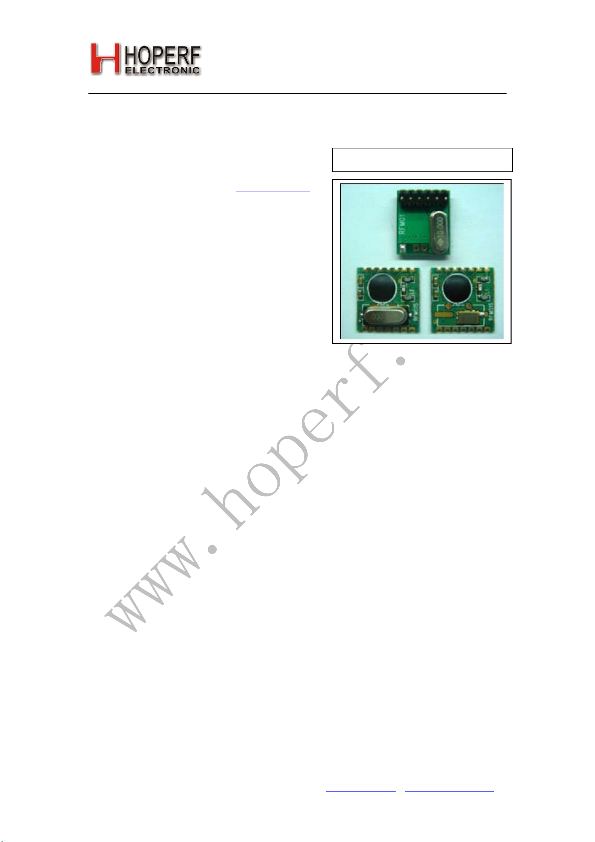
RFM01
Version: 1.2 Date: 10/17/2008
ISM BAND FSK RECEIVER MODULE
RFM01
(the purpose of this spec covers mainly for the physical
characteristic of the module, for register configure and its
related command info please refer to RF01 data sheets
)
General Introduction
RFM01 is a low costing ISM band receiver module
implemented with unique PLL and zero IF design approach.
It works with FSK modulated signal ranges from
315/433/868/915MHZ bands, comply with FCC, ETSI
regulation. The SPI interface is used to communicate with
microcontroller for parameter setting. RFM01 works with
RFM02 transmitter module. At 433MHZ band, the pair of
module can work up to 300m in the free open air.
RFM01
Features:
• Low costing, high performance and price ratio
• Tuning free during production
• FSK reception
• PLL and zero IF technology
• Fast PLL lock time
• High resolution PLL with 2.5 KHz step
• High data rate (up to 115.2 kbps with internal demodulator,with external RC filter highest data rate is
256 kbps)
• Differential antenna input
• Automatic antenna tuning
• Programmable receiver bandwidth (from 67 to 400 kHz)
• Analog and digital signal strength indicator (ARSSI/DRSSI)
• AFC
• DQD
• Internal demodulator
• SPI interface
• Clock and reset signal output for external MCU use
• 16 bits FIFO
• Low power mode (<0.5mA averaged current consumption)
• 10MHz crystal for PLL timing
• Wakeup timer
• Low battery detection
• Programmable capacitor bank
• 2.2V - 5.4V power supply
• Low power consumption
Tel: +86-755-82973805 Fax: +86-755-82973550 E-mail: sales@hoperf.com http://www.hoperf.com
Page 2
RFM01
• Stand by current less than 0.3uA
T ypical Application:
• Remote control
• Remote sensor
• Wireless data collection
• Home security system
• Toys
• Tire pressure monitoring system
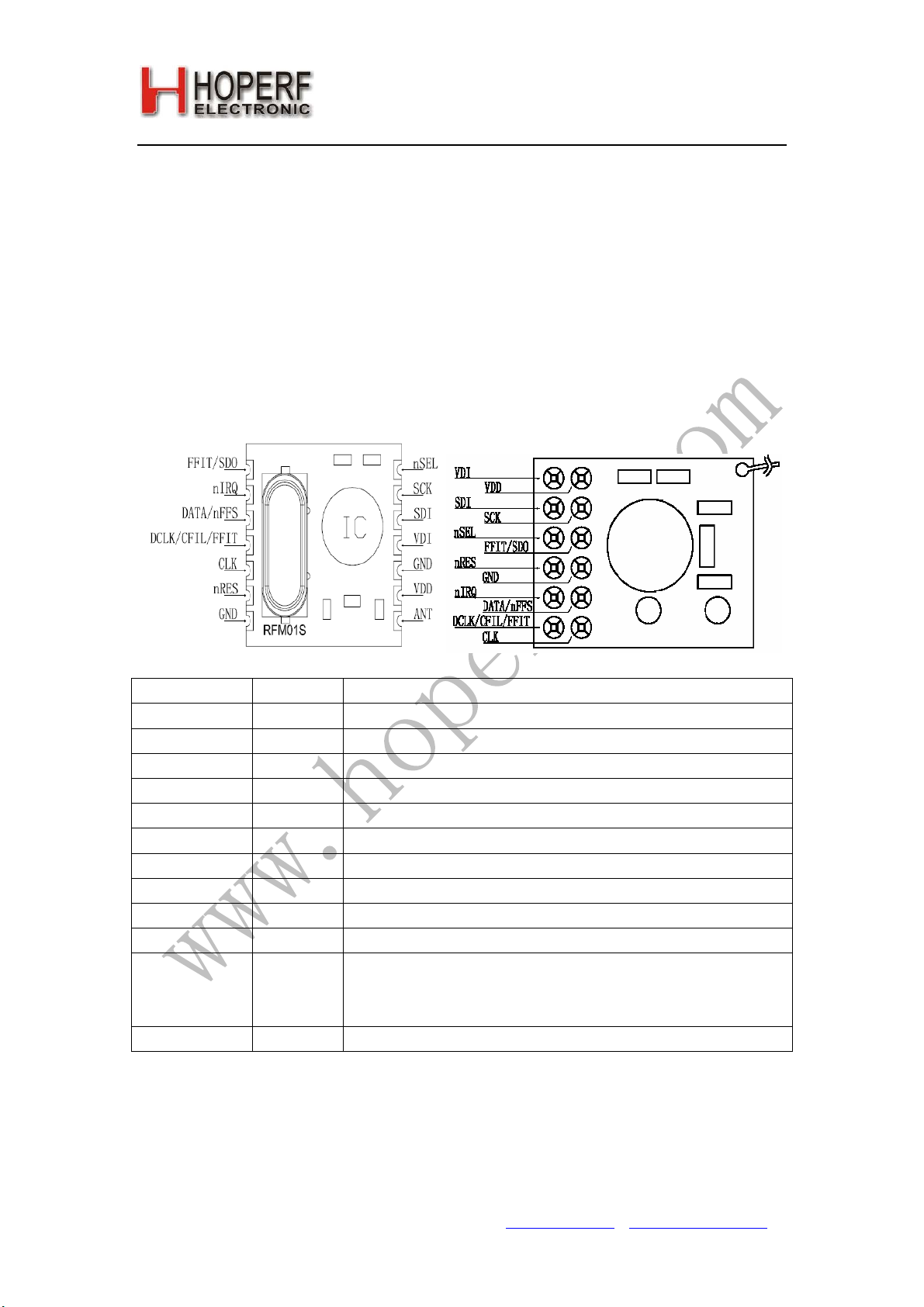
Pin Definition:
SMD DIP
Version: 1.2 Date: 10/17/2008
definition Type Function
VDI DO Valid data indicator
VDD S Positive power supply
SDI DI SPI data input
SCK DI SPI clock input
nSEL DI Chip select (active low)
FFIT/SDO DO FIFO fill interrupt(active low) or status read data output
nRES DO
GND S Power ground
nIRQ DO
DATA/nFFS DO/DI Data input(non FIFO mode)/ FIFO select
DCLK/CFIL/FFIT DO/AIO/DO
CLK DO Clock output for external microcontroller
Reset output(active low)
Interrupts request output(active low)
Clock output (no FIFO )/ external filter capacitor(analog mode)/ FIFO
interrupts(active high)when FIFO level set to 1, FIFO empty
interruption can be achieved
Tel: +86-755-82973805 Fax: +86-755-82973550 E-mail: sales@hoperf.com http://www.hoperf.com
Page 3
RFM01
Electrical Parameter:
Maximum(not at working mode)
symbol parameter minimum maximum Unit
Vdd Positive power supply -0.5 6.0 V
Vin All pin input level -0.5 Vdd+0.5 V
Iin Input current except power -25 25 MA
ESD Human body model 1000 V
Tst Storage temperature -55 125
Tld Soldering temperature(10s) 260
Recommended working range
symbol parameter minimum maximum Unit
Vdd Positive power supply 2.2 5.4 V
Top Working temperature -40 85
DC characteristic
symbol parameter Remark minimum typical maximum Unit
Idd Current consumption 315,433MHz band
868,915MHz band
Ix Stand by current Crystal and base
band on
Ipd Sleep mode current
Ilb Low battery detection 0.5 uA
Vlb Low battery step 0.1V per step 2.2 5.3 V
V
Low battery detection
lba
accuracy
Vil Low level input 0.3*Vdd V
Vih High level input 0.7*Vdd V
Iil Leakage current Vil=0V -1 1 uA
Iih Leakage current Vih=Vdd,Vdd=5.4V -1 1 uA
Vol Low level output Iol=2mA 0.4 V
Voh High level output Ioh=-2mA Vdd-0.4 V
Note: before entering sleep mode, all interrupt should be handled, otherwise the crystal oscillator still
running and consume 3mA appr. current.
AC characteristic
symbol parameter remark min typical max Unit
f
PLL frequency Parallel fundamental 8 10 12 MHz
ref
f
LO
Tel: +86-755-82973805 Fax: +86-755-82973550 E-mail: sales@hoperf.com http://www.hoperf.com
frequency
(10MHz crystal used)
All blocks off(Note)
75 mV
315 MHz band,2.5KHz step
433 MHz band,2.5KHz step
868 MHz band,5KHz step
915 MHz band,7.5KHz step
Version: 1.2 Date: 10/17/2008
℃
℃
℃
9
10.5
0.3 uA
310.24
430.24
860.48
900.72
3.0 3.5
319.75
11
12.5
439.75
879.51
929.27
mA
mA
MHz
Page 4
RFM01
f
LO
frequency
(8MHZ crystal used)
f
LO
frequency
(12MHZ crystal used)
BW
Receiver bandwidth
t
PLL lock time After 10MHz step hopping,
lock
T
PLL start time After crystal stabilized 250 us
st, p
BR Data rate With internal digital
BRA Data rate With external RC filter 256 kbps
P
min
AFC
sensitivity
AFC working range
range
RSA RSSI accuracy ±5 dB
RSR RSSI range 46 dB
C
ARSSI filter 1 nF
ARSSI
RS
RSSI programmable
STEP
step
RS
DRSSI response time RSSI output high after valid ,
RESP
CXL Capacitor bank Programmable step with
T
PWR time Vdd reach 90% 50 100 mS
POR
T
Wakeup timer period Calibrated each 30s
PBT
T
Programmable
WAKE-UP
wakeup time
TSX Crystal start up time Crystal ESR < 100 Ohms 5 mS
C
Load capacitance 2 pF
IN,D
T
Output rising edge With 15PF load 10 ns
r,F
315 MHz band,2.5KHz step
433 MHz band,2.5KHz step
868 MHz band,5KHz step
915 MHz band,7.5KHz step
315 MHz band,2.5KHz step
433 MHz band,2.5KHz step
868 MHz band,5KHz step
915 MHz band,7.5KHz step
1
2
3
4
5
6
frequency error <10 kHz
demodulator
BW=134KHz,BR=1.2kbps,315MHz band
BW=134KHz,BR=1.2kbps,433MHz band
BW=134KHz,BR=1.2kbps,868MHz band
BW=134KHz,BR=1.2kbps,915MHz band
: received signal
δF
fsk
modulation depth
6 dB
C
=5nF
ARRSI
0.5pF step, +/- 10%
1 5*10E11 mS
Version: 1.2 Date: 10/17/2008
248.19
344.19
688.38
720.57
372.28
516.28
1032.5
1080.8
60
120
180
240
300
360
255.80
351.80
703.61
743.41
383.71
527.71
1055.4
1115.1
67
134
200
270
350
400
75
150
225
300
375
450
20 us
115.2 kbps
-109 -100
-109 -100
-105 -98
-105 -98
0.8*δF
fsk
500 us
8.5 16 pF
0.96
1.08
MHz
MHz
kHz
dBm
mS
Tel: +86-755-82973805 Fax: +86-755-82973550 E-mail: sales@hoperf.com http://www.hoperf.com
Page 5

RFM01
Field testing range
Band Test condition Distance
433MHz band Receiver bandwidth =134KHz, data rate=1.2kbps, transmitter
modulation=60KHZ(matches with RF02B)
In free open area
868MHz band Receiver bandwidth=134KHz,data rate =1.2kbps
Transmitter modulation=60KHZ(matches with RFM02B)in free
open area
915MHz band Receiver bandwidth=134KHz,data rate =1.2kbps
Transmitter modulation=60KHZ(matches with RFM02B)in free
open area
Version: 1.2 Date: 10/17/2008
>300M
>200M
>200M
Mechanical Dimension
(units in mm)
SMD PACKAGE(S1)
Tel: +86-755-82973805 Fax: +86-755-82973550 E-mail: sales@hoperf.com http://www.hoperf.com
Page 6

RFM01
SMD PACKAGE(S2)
Version: 1.2 Date: 10/17/2008
DIP PACKAGE(D)
Tel: +86-755-82973805 Fax: +86-755-82973550 E-mail: sales@hoperf.com http://www.hoperf.com
Page 7

RFM01
Version: 1.2 Date: 10/17/2008
Module Model Definition
model=module-operation_band-package_type
RFM01-433-D
module type operation band Package
Note: SMD packages is divided into two kinds based on thickness: 1. thickness is 4.2mm, 2. thickness is
2.2mm
example:1,RFM01 module at 433MHz band ,DIP: RFM01-433-D。
2,RFM01 module at 868MHZ band,SMD, thickness at 4.2mm: RFM01-868-S1。
Tel: +86-755-82973805 Fax: +86-755-82973550 E-mail: sales@hoperf.com http://www.hoperf.com
Page 8

RFM01
RF01 And RFM01 Product Change Notification
Prior Product Revision #: J
New Product Revision #: J1
FUNCTION / ISSUE IMPLEMENTED CHANGES
The control of the wake up timer’s
Wake Up Timer calibration
1
internal calibration has been changed to
prevent an unnecessary Xosc on state
Version: 1.2 Date: 10/17/2008
Wake Up Timer startup
2
Unlocking of the PLL in 315 MHz
3
band
Unknown VDI state when the receiver
4
chain is switched off
When the device wakes from sleep
mode, no clock is available on the
5
CLK (PIN 8).
If the µC CLK output was used in
LPDM mode, the internal logic control
did not switch off the crystal oscillator
6
during the idle period of the LPDM
cycle.
HOPE MICROELECTRONICS CO.,LTD
Rm B.8/F LiJingGe Emperor Regency 6012
ShenNan Rd., Shenzhen,China
Tel: 86-755-82973805
Fax: 86-755-82973550
Email: sales@hoperf.com
rade@hoperf.com
t
Website: http://www.hoperf.com
http://www.hoperf.cn
http://hoperf.en.alibaba.com
The Wake Up Timer has been modified
to provide faster start up.
The reference clock duty cycle was
tuned closer to 50%, which eliminated
the 315 MHz PLL lock issues.
VDI is set to logic low when receiver
chain is switched off
The modifications eliminated this
problem.
The modifications eliminated this
blem.
This document may contain preliminary information and is subject to
change by Hope Microelectronics without notice. Hope
Microelectronics assumes no responsibility or liability for any use of
the information contained herein. Nothing in this document shall
operate as an express or implied license or indemnity under the
intellectual property rights of Hope Microelectronics or third parties.
The products described in this document are not intended for use in
implantation or other direct life support applications where malfunction
may result in the direct physical harm or injury to persons. NO
WARRANTIES OF ANY KIND, INCLUDING, BUT NOT LIMITED TO,
THE IMPLIED WARRANTIES OF MECHANTABILITY OR FITNESS
FOR A ARTICULAR PURPOSE, ARE OFFERED IN THIS
DOCUMENT.
©2008, HOPE MICROELECTRONICS CO.,LTD. All rights reserved.
Tel: +86-755-82973805 Fax: +86-755-82973550 E-mail: sales@hoperf.com http://www.hoperf.com
 Loading...