

Page 1

RF22
Version: 0.1 Date: 12/23/2008
RF22 Universal ISM Band FSK Transceiver
Features
Frequency range = 240–930 MHz
z
z Sensitivity = –118dBm
z +20 dBm Max Output Power
Configurable +11 to +20 dBm
z Low Power Consumption
18.5 mA receive
27mA @ +11dBm
z Data Rate = 1 to 128kbps
z Power Supply = 1.8 to 3.6V
z Ultra low power shutdown mode
z Digital RSSI
z Wake-on-radio
z Auto-frequency calibration (AFC)
z Antenna diversity & TR switch control
z Configurable packet structure
z Preamble detector
z TX & RX 64 byte FIFOs
z Low battery detector
z Temperature sensor and 8-bit ADC
z –40 to +85oC temperature range
z Integrated voltage regulators
z Frequency hopping capability
z On-chip crystal tuning
z 20-Pin QFN package
z FSK, GFSK, and OOK modulation
z Low BOM
z Power-on-reset (POR)
The RF22 offers advanced radio features including continuous frequency coverage from 240–930 MHz and adjustable output power
of up to +20 dBm. The RF22’s high level of integration offers reduced BOM cost while simplifying the overall system design. The
extremely low receive sensitivity (–118 dBm) coupled with industry leading +20 dBm output power ensures extended range and
improved link performance. Built-in antenna diversity and support for frequency hopping can be used to further extend range and
enhance performance.
Additional system features such as an automatic wake-up timer, low battery detector, 64 byte TX/RX FIFOs, automatic packet
handling, and preamble detection reduce overall current consumption and allow the use of lower-cost system MCUs. An integrated
temperature sensor, general purpose ADC, poweron- reset (POR), and GPIOs further reduce overall system cost and size.
The RF22’s digital receive architecture features a high-performance ADC and DSP based modem which performs demodulation,
filtering, and packet handling for increased performance. This digital architecture simplifies system design while allowing for the use
of lower-end MCUs. The direct digital transmit modulation and automatic PA power ramping ensure precise transmit modulation and
reduced spectral spreading ensuring compliance with FCC and ETSI regulations.
Applications
z Remote control
z Home security & alarm
z Telemetry
z Personal data logging
z Toy control
z Tire Pressure monitoring
z Wireless PC peripherals
z Remote meter reading
z Remote keyless entry
z Home automation
z Industrial control
z Sensor networks
z Health monitors
z Tag readers
Tel: +86-755-82973805 Fax: +86-755-82973550 E-mail: sales@hoperf.com http://www.hoperf.com
1
Page 2
RF22
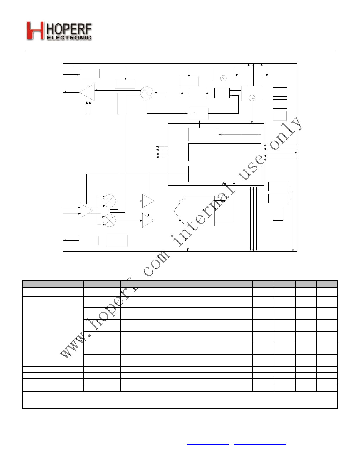
Functional Block Diagram
Version: 0.1 Date: 12/23/2008
VDD_RF
TX
RFp
RFn
VR_IF
RF LDO
PA
PMAR_AP
LNA
IF LDO
RC 32K OSC
LPF
PLL LDO
ADC_REF
CP
N
Delta Sigma
Modulator
ADC
PFD
TXMOD
SPI, & Controller
Digital Modem
VCO LDO
LRT
C
_RWP
Mixers
BIAS
VCO
ANTDIV
TXRXSW
PA_RAMP
PWR_CTRL
AGC Control
PGA
SDN
Xin
Xout
30M XTAL
OSC
Digital Logic
GPIO_0
nSEL
VDD_DIG
LBD
Temp
Sensor
8Bit
ADC
SCLK
SDI
SDO
VDD_DIG
GND_DIG
Low Power
Digital LDO
Digital LDO
POR
GPIO_1
GPIO_2
VR_DIG
1. Electrical Specifications
Table1. DC Characteristics
Parameter Symbol Conditions Min Typ Max Units
Supply Voltage Range Vdd
I
Shutdown
Power Saving Modes
TUNE Mode Current I
I
Standby
I
Sleep
2
I
Sensor-LBD
I
Sensor-TS
I
Ready
Tune
RX Mode Current IRX — 18.5 TBD mA
I
TX_+20
I
TX_+11
Notes:
1. All specification guaranteed by production test unless otherwise noted.
2. Guaranteed by qualification.
1
RC Oscillator, Main Digital Regulator,
and Low Power Digital Regulator OFF
Low Power Digital Regulator ON (Register values retained)
and Main Digital Regulator, and RC Oscillator OFF
2
2
RC Oscillator and Low Power Digital Regulator ON
(Register values retained) and Main Digital Regulator OFF
Main Digital Regulator and Low Battery Detector ON,
Crystal Oscillator and all other blocks OFF
Main Digital Regulator and Temperature Sensor ON,
Crystal Oscillator and all other blocks OFF
2
2
Crystal Oscillator and Main Digital Regulator ON,
1.8 3.0 3.6 V
— 10 TBD nA
— 400 TBD nA
— 800 TBD nA
2
— 1 TBD A
— 1 TBD A
— 600 TBD A
all other blocks OFF. Crystal Oscillator buffer disabled
Synthesizer and regulators enabled — 9.5 TBD mA
txpow[1:0] = 11 (+20 dBm), VDD = 3.3 V — 60 TBD mA TX Mode Current
txpow[1:0] = 00 (+11 dBm), VDD = 3.3 V — 27 TBD mA
Tel: +86-755-82973805 Fax: +86-755-82973550 E-mail: sales@hoperf.com http://www.hoperf.com
2
Page 3
RF22
Table2. Synthesizer AC Electrical Characteristics
Parameter Symbol Conditions Min Typ Max Units
F
Low Band 240 — 480 MHz
2
Synthesizer Frequency Range
Reference Frequency f
Reference Frequency Input Level
Synthesizer Settling Time
Residual FM
2
2
2
Phase Noise
2
SYNTH-LB
F
F
F
f
High Band 480 — 930 MHz
SYNTH-HB
Low Band — 156.25 — Hz Synthesizer Frequency Resolution
RES-LB
High Band — 312.5 — Hz
RES-HB
f
REF
When using reference frequency instead of crystal.
REF_LV
/ 3 — 10 — MHz
crystal
Measured peak-to-peak (V
Measured from leaving Ready mode with XOSC
t
LOCK
Running to any frequency including VCO Calibration
F
Integrated over ±250 kHz bandwidth
RMS
(500 Hz lower bound of integration)
L(f
M
F = 10 kHz — –80 TBD dBc/Hz
)
F = 100 kHz — –90 TBD dBc/Hz
F = 1 MHz — –115 TBD dBc/Hz
F = 10 MHz — –130 TBD dBc/Hz
P
< 1 GHz — — –54 dBm
Spurious Emissions
2
OB-TX1
1–12.75 GHz, non-intentional radiator — — –54 dBm
P
OB-TX2
Notes:
1. All specification guaranteed by production test unless otherwise noted.
2. Guaranteed by qualification.
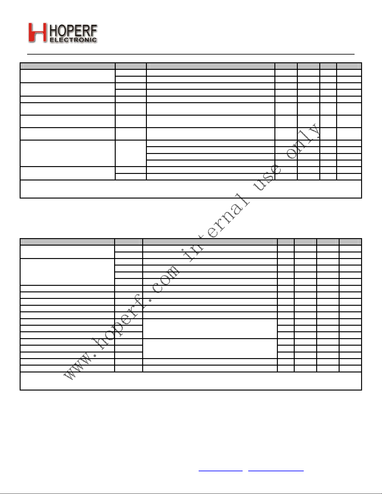
Table3. Receiver AC Electrical Characteristics
Parameter Symbol Conditions Min Typ Max Units
F
Low Band 240 — 480 MHz
RX Frequency Range
RX Sensitivity
2
SYNTH-LB
F
P
P
P
P
High Band 480 — 930 MHz
SYNTH-HB
(BER < 0.1%) (2 kbps, GFSK, BT=0.5, f = ±5 kHz)1 — –117 TBD dBm
RX_2
(BER < 0.1%) (40 kbps, GFSK, BT=0.5, f = ±20 kHz)1 — –106 TBD dBm
RX_40
(BER < 0.1%) (100 kbps, GFSK, BT=0.5, f =±50 kHz)2 — –102 TBD dBm
RX_100
(BER < 0.1%) (4.8 kbps, OOK)1 — –110 TBD dBm
RX_OOK
RX Bandwidth BW 2.6 — 620 kHz
Residual BER Performance2 P
Up to +5dBm Input Level — 0 0.1 ppm
RX_RES
Input Intercept Point, 3rd Order2 IIP3RX f1 = 915MHz, f2 = 915MHz, P1 = P2= –40dBm — –20 TBD dBm
LNA Input Impedance R
RSSI Resolution RES
±1-Ch Offset Selectivity2 (BER < 0.1%) C/I
±2-Ch Offset Selectivity2 (BER < 0.1%) C/I
±3-Ch Offset Selectivity2 (BER < 0.1%) C/I
Blocking at 1 MHz2 1M
Blocking at 4 MHz2 4M
Blocking at 8 MHz2 8M
Image Rejection Im
Spurious Emissions2 P
Unmatched, measured differentially across RX input pins — 250 —
IN-RX
— ±0.5 — dB
RSSI
Desired Ref Signal 3 dB above sensitivity. Interferer and
— –31 TBD dB
1-CH
2-CH
3-CH
BLOCK
BLOCK
BLOCK
REJ
OB_RX1
desired modulated with 40 kbps F = 20 kHz GFSK with
— –35 TBD dB
BT = 0.5, channel spacing = 150 kHz
Desired Ref Signal 3 dB above sensitivity. Interferer and
— –52 TBD dB
desired modulated with 40 kbps F = 20 kHz GFSK with
— –56 TBD dB
BT = 0.5
IF=937 kHz — –30 — dB
Measured at RX pins (LO feed through) — — –54 dBm
Notes:
1. All specification guaranteed by production test unless otherwise noted.
2. Guaranteed by qualification.
1
)
PP
1
Version: 0.1 Date: 12/23/2008
0.7 — 1.6 V
— 200 TBD s
— 2 4 kHz
— –40 TBD dB
— –63 TBD dB
RMS
Tel: +86-755-82973805 Fax: +86-755-82973550 E-mail: sales@hoperf.com http://www.hoperf.com
3
Page 4
RF22
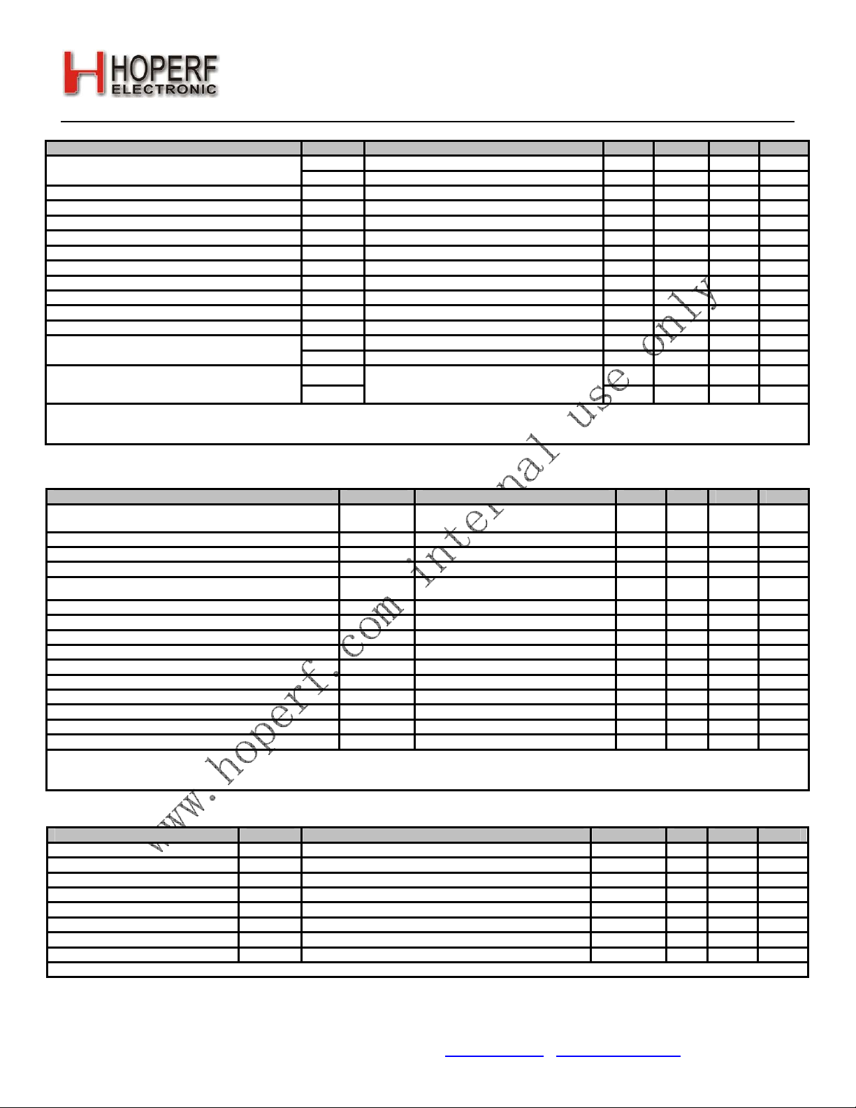
Table4. Transmitter AC Electrical Characteristics1
Parameter Symbol Conditions Min Typ Max Units
F
Low Band 240 — 480 MHz
2
TX Frequency Range
FSK Modulation Data Rate2 DR
OOK Modulation Data Rate2 DR
Modulation Deviation2 f ±0.625 ±320 kHz
Modulation Deviation Resolution f
Output Power Range2 P
TX RF Output Steps2 P
TX RF Output Level Variation vs. Voltage2 P
TX RF Output Level2 Variation vs. Temperature P
TX RF Output Level Variation vs. Frequency2 P
Transmit Modulation Filtering B*T Gaussian Filtering Bandwith Time Product — 0.5 —
2
Spurious Emissions
Harmonics
2
Notes:
1. All specification guaranteed by production test unless otherwise noted.
2. Guaranteed by qualification.
Table5. Auxiliary Block Specifications1
Parameter Symbol Conditions Min Typ Max Units
Temperature Sensor Accuracy2 TSA When calibrated using temp
Temperature Sensor Sensitivity2 TSS — 5 — mV/°C
Low Battery Detector Resolution2 LBD
Low Battery Detector Conversion Time2 LBDCT — 250 — s
Microcontroller Clock Output Frequency2 MC
General Purpose ADC Accuracy ADC
General Purpose ADC Resolution ADC
Temp Sensor & General Purpose ADC Conversion Time ADCCT — 305 — sec
30 MHz XTAL Start-Up time t
30 MHz XTAL Cap Resolution 30M
32 kHz XTAL Start-Up Time t
32 kHz XTAL Accuracy 32K
32 kHz RC OSC Accuracy 32KRC
POR Reset Time t
Software Reset Time t
Notes:
1. All specification guaranteed by production test unless otherwise noted.
2. Guaranteed by qualification.
Table6. Digital IO Specifications (SDO, SDI, SCLK, nSEL, and nIRQ)
Parameter Symbol Conditions Min Typ Max Units
Rise Time T
Fall Time T
0.1 x VDD to 0.9 x VDD, CL= 5 pF — — 8 ns
RISE
0.9 x VDD to 0.1 x VDD, CL= 5 pF — — 8 ns
FALL
Input Capacitance CIN — — 1 pF
Logic High Level Input Voltage VIH V
Logic Low Level Input Voltage VIL — 0.6 V
Input Current IIN 0<VIN< VDD –100 — 100 nA
Logic High Level Output Voltage VOH I
Logic Low Level Output Voltage VOL I
Note: All specification guaranteed by production test unless otherwise noted.
SYNTH-LB
F
SYNTH-HB
FSK
OOK
RES
Tested at 915 MHz, txpow[1:0] = 11 +11 — +20 dBm
TX
RF_OUT
RF_V
RF_TEMP
RF_FREQ
P
OB-TX1
P
OB-TX2
P
2HARM
P
3HARM
High Band 480 — 930 MHz
1 — 128 kbps
1.2 — 40 kbps
— 0.625 — kHz
TXPWR[1:0] = 00 thru 11 TBD 3 TBD dB
Measured from VDD=3.6 V to VDD=1.8 V — 2 TBD dB
–40 to +85oC — 2 TBD dB
Measured across any one frequency band — 1 TBD dB
POUT = 11 dBm, Frequencies <1 GHz — — –54 dBm
1–12.75 GHz, excluding harmonics — — –54 dBm
Using Reference Design TX Matching Network
— — –42 dBm
and Filter with Max Output Power (20 dBm).
Harmonics reduce linearly with output power
sensor offset register
— 50 — mV
RES
Configurable to 30 MHz, 15 MHz, 10 MHz,
4 MHz, 3 MHz, 2 MHz, 1 MHz, or 32.768 kHz
— 8 — bit
ENB
— 4 — mV
RES
— 1 — ms
30M
— 97 — fF
RES
— 6 — sec
32k
— 100 — ppm
RES
— 2500 — ppm
RES
— 16 — ms
POR
— 100 — s
soft
< 1mA source, VDD=1.8 V VDD – 0.6 — — V
OH
<1 mA sink, VDD=1.8 V — — 0.6 V
OL
Version: 0.1 Date: 12/23/2008
— — –42 dBm
— 0.5 — °C
32768 — 30M Hz
– 0.6 — — V
DD
Tel: +86-755-82973805 Fax: +86-755-82973550 E-mail: sales@hoperf.com http://www.hoperf.com
4
Page 5
RF22
Table7. GPIO Specifications (GPIO_0, GPIO_1, and GPIO_2)
Parameter Symbol Conditions Min Typ Max Units
Rise Time T
Fall Time T
Input Capacitance CIN — — 1 pF
Logic High Level Input Voltage VIH V
Logic Low Level Input Voltage VIL — — 0.6 V
Input Current IIN 0<VIN< VDD –100 — 100 nA
Input Current If Pullup is Activated I
Maximum Output Current
Logic High Level Output Voltage VOH I
Logic Low Level Output Voltage VOL I
Note: All specification guaranteed by production test unless otherwise noted.
0.1 x VDD to 0.9 x VDD, CL= 10 pF, DRV<1:0>=HH — — 8 ns
RISE
0.9 x VDD to 0.1 x VDD, CL= 10 pF, DRV<1:0>=HH — — 8 ns
FALL
V
INP
I
DRV<1:0>=LL 0.1 0.5 0.8 mA
OmaxLL
I
DRV<1:0>=LH 0.9 2.3 3.5 mA
OmaxLH
I
DRV<1:0>=HL 1.5 3.1 4.8 mA
OmaxHL
I
DRV<1:0>=HH 1.8 3.6 5.4 mA
OmaxHH
=0 V 5 — 25 A
IL
< I
source, VDD=1.8 V VDD – 0.6 — — V
OH
Omax
< I
sink, VDD=1.8 V — — 0.6 V
OL
Omax
Table8. Absolute Maximum Ratings
Parameter Value Units
VDD to GND –0.3, +3.6 V
VDD to GND on TX Output Pin –0.3, +8.0 V
Voltage on Digital Control Inputs –0.3, V
Voltage on Analog Inputs –0.3, VDD + 0.3 V
RX Input Power +10 dBm
Operating Ambient Temperature Range TA –40 to +85 °C
Thermal Impedance JA 30 °C/W
Junction Temperature TJ +125 °C
Storage Temperature Range T
Note:
Stresses beyond those listed under “Absolute Maximum Ratings” may cause permanent damage to the device.
These are stress ratings only and functional operation of the device at or beyond these ratings in the operational sections of the specifications is not
implied. Exposure to absolute maximum rating conditions for extended periods may affect device reliability.
Caution: ESD sensitive device.
Power Amplifier may be damaged if switched on without proper load connected.
–55 to +125 °C
STG
Version: 0.1 Date: 12/23/2008
– 0.6 — V
DD
+ 0.3 V
DD
1.1. Definition of Test Conditions
Production Test Conditions:
T
A
V
DD
External reference signal (XIN) = 1.0 V
Production test schematic (unless noted otherwise)
All RF input and output levels referred to the pins of the RF22 (not the RF module)
Extreme Test Conditions:
T
A
V
DD
External reference signal (XIN) = 0.7 to 1.6 V
Production test schematic (unless noted otherwise)
All RF input and output levels referred to the pins of the RF22 (not the RF module)
o
= +25
= –40 to +85
C
= +3.3 VDC
o
C
= +1.8 to +3.6 VDC
Tel: +86-755-82973805 Fax: +86-755-82973550 E-mail: sales@hoperf.com http://www.hoperf.com
at 30 MHz, centered around 0.8 VDC
PP
at 30 MHz centered around 0.8 VDC
PP
5
Page 6

RF22
Test Notes:
All electrical parameters with Min/Max values are guaranteed by one (or more) of the following test methods.
Electrical parameters shown with only typical values are not guaranteed.
Guaranteed by design and/or simulation but not tested.
Guaranteed by Engineering Qualification testing at Extreme Test Conditions.
Guaranteed by 100% Production Test Screening at Production Test Conditions.
2. Functional Description
The RF22 is a 100% CMOS ISM wireless transceiver with continuous frequency tuning over the complete 240–930
MHz band. The wide operating voltage range of 1.8–3.6 V and low current consumption makes the RF22 and ideal
solution for battery powered applications.
The RF22 operates as a time division duplexing (TDD) transceiver where the device alternately transmits and receives
data packets. The receiver uses a singleconversion, image-reject mixer to downconvert the 2-level FSK/GFSK/OOK
modulated receive signal to a low IF frequency. Following a programmable gain amplifier (PGA) the signal is converted
to the digital domain by a high performance - ADC allowing filtering, demodulation, slicing, error correction, and
packet handling to be performed in the built-in DSP increasing the receiver’s performance and flexibility versus analog
based architectures. The demodulated signal is then output to the system MCU through a programmable GPIO or via
the standard SPI bus by reading the 64-byte RX FIFO.
A single high precision local oscillator (LO) is used for both transmit and receive modes since the transmitter and
receiver do not operate at the same time. The LO is generated by an integrated VCO and - Fractional-N PLL
synthesizer. The synthesizer is designed to support configurable data rates, output frequency, frequency deviation,
and Gaussian filtering at any frequency between 240–930 MHz. The transmit FSK data is modulated directly into the
- data stream and can be shaped by a Gaussian low-pass filter to reduce unwanted spectral content.
The PA output power can be configured between +11 and +20 dBm in 3 dB steps. The PA is single-ended to allow for
easy antenna matching and low BOM cost. The PA incorporates automatic ramp-up and rampdown control to reduce
unwanted spectral spreading. This RF22 supports frequency hopping, TX/RX switch control, and antenna diversity
switch control to extend the link range and improve performance. Antenna diversity is completely integrated into the
RF22 and can improve the system link budget by 8–10 dB (according to published papers on Antenna Diversity)
resulting in substantial range increases depending on the environmental conditions. The +20 dBm power amplifier can
also be used to compensate for the reduced performance of a lower cost antenna or antenna with size constraints due
to a small form-factor. Competing solutions require large and expensive external PAs to achieve comparable
performance.
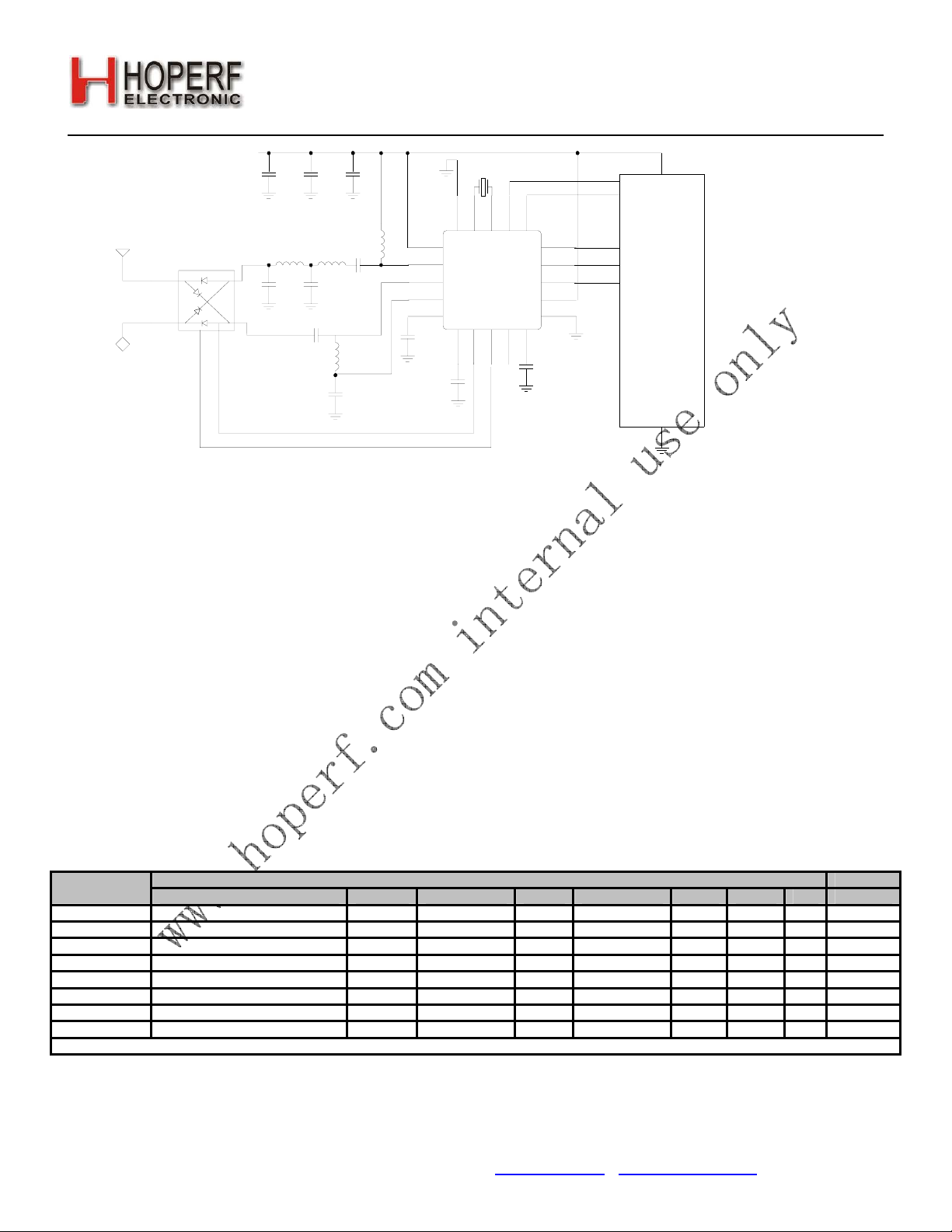
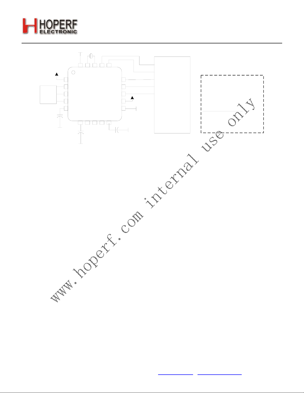
The RF22 is designed to work with a microcontroller, crystal, and a few passives to create a very low cost system as
shown Figure 1. Voltage regulators are integrated on-chip which allow for a wide range of operating supply voltage
conditions from +1.8 to +3.6 V. A standard 3 or 4-pin SPI bus is used to communicate with the microcontroller. Three
configurable general purpose I/Os are available for use to tailor towards the needs of the system. A more complete list
of the available GPIO functions is shown in "8. Auxiliary Functions" on page 53 but just to name a few, microcontroller
clock output, Antenna Diversity, TRSW control, POR, and specific interrupts. A limited number of passive components
are needed to match the LNA and PA; refer to "9. Reference Design" on page 70 for the required component values at
different frequency ranges.
The application shown in Figure 1 is designed for a system with Antenna Diversity. The Antenna Diversity Control
Algorithm is completely integrated into the chip and is discussed further in "8.9. Antenna-Diversity" on page 66.
For a simpler application example not using Antenna Diversity see the "9. Reference Design" on page 70.
Version: 0.1 Date: 12/23/2008
Tel: +86-755-82973805 Fax: +86-755-82973550 E-mail: sales@hoperf.com http://www.hoperf.com
6
Page 7
RF22
supply voltage
TR & ANT-DIV
Switch
C6
100p
L3L2
C3 C2
C7
100n
C4
L4
C5
C8
1u
VDD_RF
L1
TX
C1
Programmable load capacitors for X1 are integrated.
R1, L1-L5 and C1-C4 values depend on frequency band,
antenna impedance, output power and supply voltage range.
RXp
RXn
VR_IF
C10
1u
Figure1. +20dBm Application with Antenna Diversity and FHSS
2.1. Operating Modes
The RF22 provides several modes of operation which can be used to optimize the power consumption of the device
application. Depending upon the system communication protocol, the optimal trade-off between the radio wake time
and power consumption can be achieved.
Table 9 summarizes the modes of operation of the RF22. In general, any given mode of operation may be classified as
an Active mode or a Power Saving mode. The table indicates which block(s) are enabled (active) in each
corresponding mode. With the exception the Shutdown mode, all can be dynamically selected by sending the
appropriate commands over the SPI in order to optimize the average current consumption. An “X” in any cell means
that: in the given mode of operation, that block can be independently programmed to be either ON or OFF, without
noticeably affecting the current consumption. The SPI circuit block includes the SPI interface and the register space.
The 32 kHz OSC circuit block includes the 32.768 kHz RC oscillator or 32.768 kHz crystal oscillator, and wake-up timer.
AUX (Auxiliary Blocks) includes the temperature sensor, general purpose ADC, and low-battery detector.
C8
X1
30MHz
TU
LE
NIX
02
91
RF22
6
7
0
O
IP
G
Q
RIn
O
X
817161
8
2
1
O
O
IP
IP
G
G
S
n
SCLK
15
SDI
14
SDO
13
VDD_D
12
GND_D
11
01
9
G
ID_RV
C9
1u
ND
S
1
2
3
4
5
FER_
C
DA
1u
Version: 0.1 Date: 12/23/2008
GP1
GP2
GP3
GP4
GP5
VDD
microcontroller
VSS
Table9. Operating Modes
Mode Name
Digital LDO SPI 32 kHz OSC AUX 30 MHz XTAL PLL PA RX I
Shutdown OFF (Register contents lost) OFF OFF OFF OFF OFF OFF OFF 10 nA
Standby ON (Register contents retained) ON OFF OFF OFF OFF OFF OFF 400 nA
Sleep ON ON X OFF OFF OFF OFF 800 nA
Sensor ON X ON OFF OFF OFF OFF 1 A
Ready ON X X ON OFF OFF OFF 600 A
Tuning ON X X ON ON OFF OFF 9.5 mA
Transmit ON X X ON ON ON OFF 27 mA*
Receive ON X X ON ON OFF ON 18.5 mA
*Note: 27 mA at +11 dBm.
Circuit Blocks
VDD
Tel: +86-755-82973805 Fax: +86-755-82973550 E-mail: sales@hoperf.com http://www.hoperf.com
7
Page 8
RF22
NW
O
DPMARAP
XTAL Settling
Time
~1ms
LA
0TLLP
S
TLLP
C
LLP
45us, may be skiped
XTAL Settling
Time
~1ms
YALEDD
PMARAPERP
PUPMARAP
LACLLP
0TLLP
S
TLLP
O
MXT
6us, Fixed
1.5Bits@DR
45us, may be skiped
TX Packet
Version: 0.1 Date: 12/23/2008
RX Packet
Configurable 0~70us, Default=20us
Configurable 5~20us, Recommended 5us
Configurable 0~310us, Recommended 100us
Configurable 0~70us, Default=20us
Configurable 0~310us, Recommended 100us
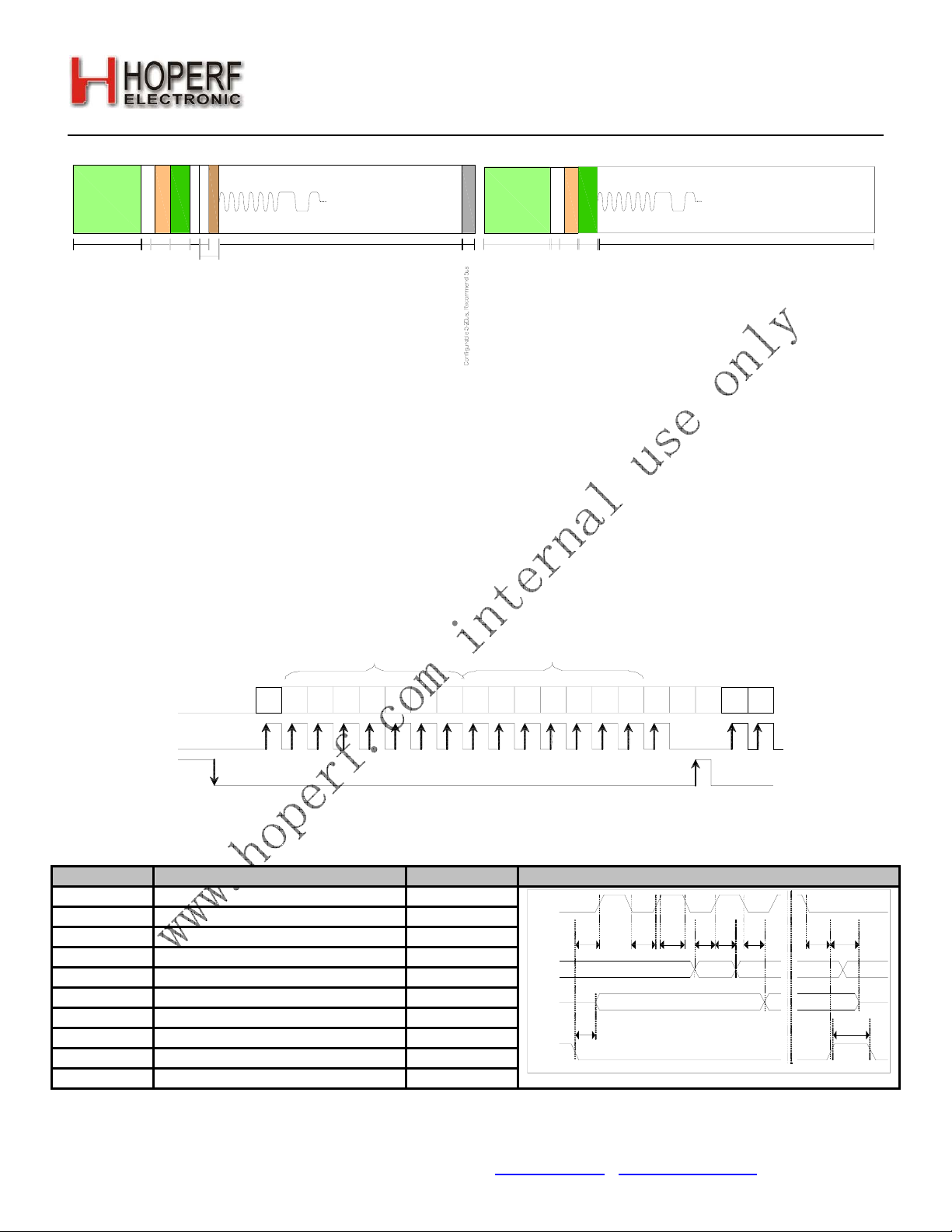
Figure2. TX Timing. Figure3. RX Timing
3. Controller Interface
3.1. Serial Peripheral Interface (SPI)
The RF22 communicates with the host MCU over a 3 wire SPI interface: SCLK, SDI, and nSEL. The host MCU can
also read data from internal registers on the SDO output pin. A SPI transaction is a 16-bit sequence which consists of a
Read-Write (R/W) select bit, followed by a 7-bit address field (ADDR), and an 8-bit data field (DATA), as demonstrated
in Figure 4. The 7-bit address field supports reading from or writing to one of the 128, 8-bit control registers. The R/W
select bit determines whether the SPI transaction is a write or read transaction. If R/W = 1, it signifies a WRITE
transaction, while R/W = 0 signifies a READ transaction. The contents (ADDR or DATA) are latched into the RF22
every eight clock cycles. The timing parameters for the SPI interface are shown in Table 10. The SCLK rate is flexible
with a maximum rate of 10 MHz.
Data
LSBMSB
SDI
SCLK
nSEL
Address
RW A5 A3 RW A7A6 xxxxA4 D0A2 A1 A0 D7 D6 D5 D4 D3 D2 D1
Figure4. SPI Timing
Table10. Serial Interface Timing Parameters
Symbol Parameter Min (nsec) Diagram
tCH Clock high time 40
SCLK
tCL Clock low time 40
tDS Data setup time 20
tDH Data hold time 20
tDD Output data delay time 20
tEN Output enable time 20
tDE Output disable time 50
SDI
SDO
t
tSS Select setup time 20
tSH Select hold time 50
nSEL
tSW Select high period 80
Tel: +86-755-82973805 Fax: +86-755-82973550 E-mail: sales@hoperf.com http://www.hoperf.com
t
SS
NE
t
t
CH
CL
t
tDSt
DD
DH
tSHt
DE
t
SW
8
Page 9
RF22
To read back data from the RF22, the R/W bit must be set to 0 followed by the 7-bit address of the register from which
to read. The 8 bit DATA field following the 7-bit ADDR field is ignored when R/W = 0. The next eight positive edge
transitions of the SCLK signal will clock out the contents of the selected register. The data read from the selected
register will be available on the SDO output pin. The READ function is shown in Figure 5. After the READ function is
completed the SDO pin will remain at either logic 1 or logic 0 state depending on the last data bit clocked out (D0).
When nSEL goes high the SDO output pin will be pulled high by internal pull-up.
SDI
SCLK
SDO
nSEL
RW
=0
A6
A5
A4
A3
A1A2D7A0
D7
Figure5. SPI Timing—READ Mode
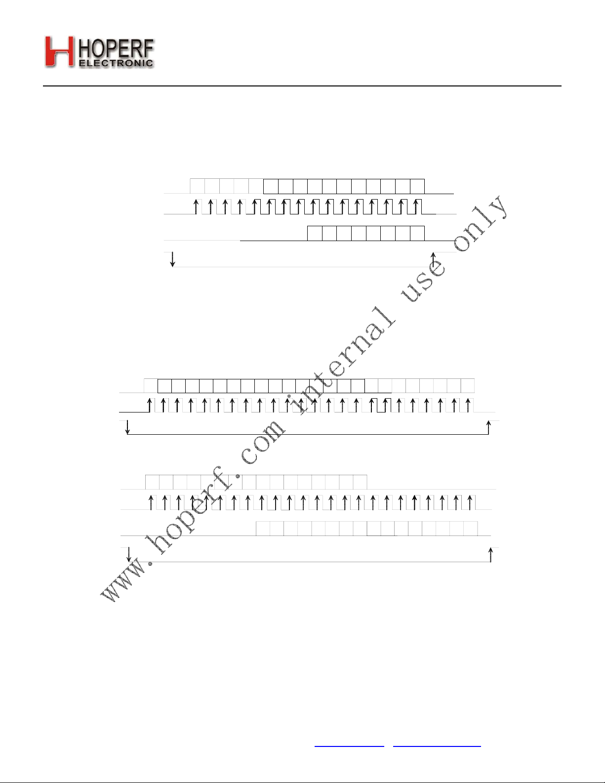
The SPI interface contains a burst read/write mode which will allows for reading/writing sequential registers without
having to re-send the SPI address. When the nSEL bit is held low while continuing to send SCLK pulses, the SPI
interface will automatically increment the ADDR and read from/write to the next address. An SPI burst write transaction
is demonstrated in Figure 6 and burst read in Figure 7. As long as nSEL is held low, input data will be latched into the
RF22 every eight SCLK cycles. A burst read transaction is also demonstrated in Figure 7.
SDI
First Bit
RW
=1
A6
A5
A4
A3 A2=XA1D7A0
D5
D4
D6
=X
=X
=X
D5
D3
D4
D6
=X
=X
D6 D5 D4 D3 D2 D1 D0
D2
D3
=X
=X
=X
=X
=X
D7
D0
D1
=X
=X
=X
Version: 0.1 Date: 12/23/2008
Last BitFirst Bit
D0
D1
D2
=X
=X
=X
Last BitFirst Bit
D5
D3
D4
D6
=X
=X
=X
=X
Last Bit
D0
D1
D2
=X
=X
=X
SCLK
nSEL
Figure6. SPI Timing—Burst Write Mode
SDI
SCLK
SDO
nSEL
First Bit
RW
A5
A6
=0
A4
A3 A2
A1D7A0
=X
First Bit
D7
D6 D5 D4 D3 D2 D1 D0
Last Bit
D0
D1
D2
D3=X4D=X5D=XD6
=X
=X
=X
=X
D7 D6 D5 D4
D1 D0D2D3
Figure7. SPI Timing—Burst Read Mode
3.2. Operating Mode Control
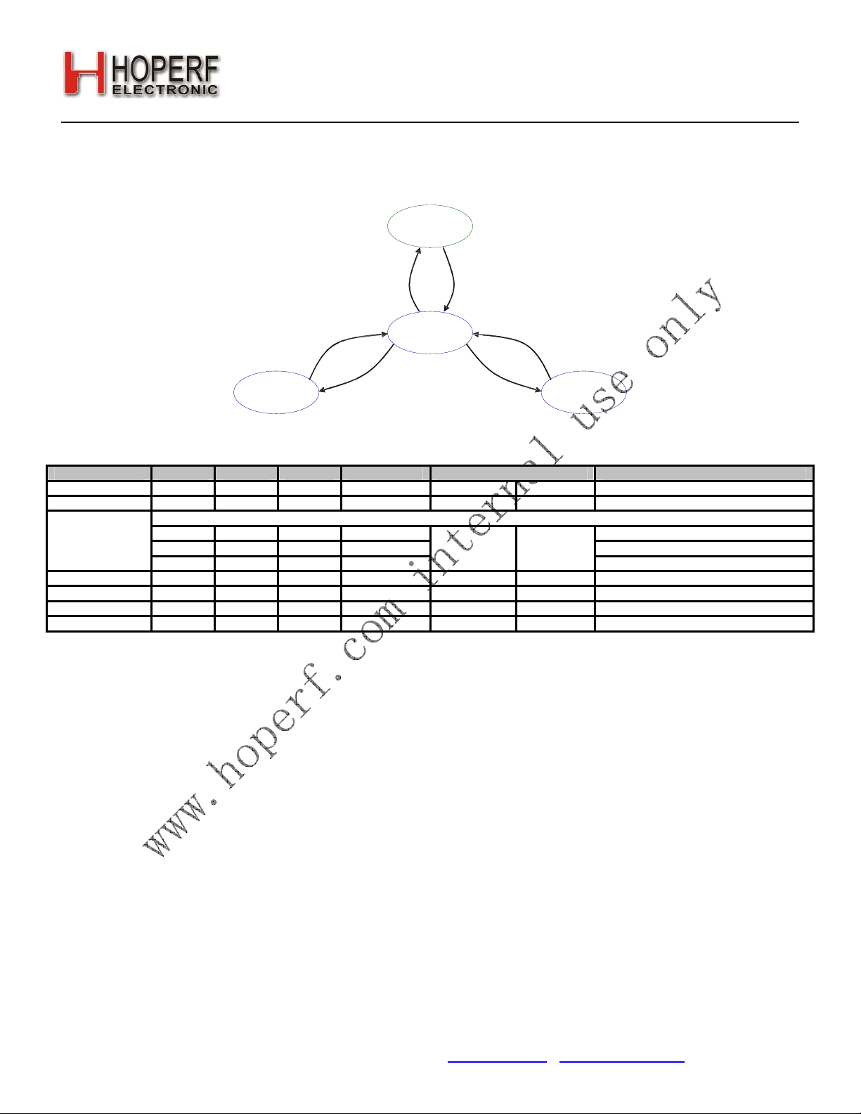
There are four primary states in the RF22 radio state machine: SHUTDOWN, IDLE, TX, and RX (see Figure 8). The
SHUTDOWN state completely shuts down the radio to minimize current consumption. There are five different
configurations/options for the IDLE state which can be selected to optimize the chip to the applications needs.
"Register 07h. Operating Mode and Function Control 1" controls which operating mode/state is selected. The TX and
RX state may be reached automatically from any of the IDLE states by setting the txon/rxon bits in "Register 07h.
Operating Mode and Function Control 1". Table 11 shows each of the operating modes with the time required to reach
either RX or TX mode as well as the current consumption of each mode.
Tel: +86-755-82973805 Fax: +86-755-82973550 E-mail: sales@hoperf.com http://www.hoperf.com
9
Page 10
RF22
The output of the LPLDO is internally connected in parallel to the output of the main digital regulator (and is available
externally at the VR_DIG pin); this common digital supply voltage is connected to all digital circuit blocks, including the
digital modem, crystal oscillator, and SPI and register space. The LPLDO has extremely low quiescent current
consumption but limited current supply capability; it is used only in the IDLE-STANDBY and IDLE-SLEEP modes.
SHUT DWN
IDLE*
TX RX
*Five Different Options for IDLE
Figure8. State Machine Diagram
Table11. Operating Modes
State/Mode xtal pll wt LBD or TS Response time to Current in State /Mode [μA]
TX RX
Shut Down State X X X X 16.21 ms 16.21 ms
Idle States:
Standby Mode
Sleep Mode
Sensor Mode
Ready Mode 1 0 X X 210 s 210 s 600 A
Tune Mode 1 1 X X 200 s 200 s 9.5 mA
TX State 1 1 X X NA 200 s 60 mA @ +20 dBm, 27 mA @ +11 dBm
RX State 1 1 X X 200 s NA 18.5 mA
0 0 0 0 400 nA
0 0 1 0 800 nA
0 0 X 1
1.21 ms
1.21 ms
Version: 0.1 Date: 12/23/2008
1 A
3.2.1. Shutdown State
The shutdown state is the lowest current consumption state of the device with nominally 5 nA of current consumption.
The shutdown state may be entered by driving the SDN pin (Pin 20) high. The SDN pin should be held low in all states
except the SHUTDOWN state. In the SHUTDOWN state, the contents of the registers are lost and there is no SPI
access.
When the chip is connected to the power supply, a POR will be initiated after the falling edge of SDN.
3.2.2. Idle State
There are five different modes in the IDLE state which may be selected by "Register 07h. Operating Mode and
Function Control 1". All modes have a tradeoff between current consumption and response time to TX/RX mode. This
tradeoff is shown in Table 11. After the POR event, SWRESET, or exiting from the SHUTDOWN state the chip will
default to the IDLE-READY mode. After a POR event the interrupt registers must be read to properly enter the SLEEP,
SENSOR, or STANDBY mode and to control the 32 kHz clock correctly.
3.2.2.1. STANDBY Mode
STANDBY mode has the lowest current consumption possible with only the LPLDO enabled to maintain the register
values. In this mode the registers can be accessed in both read and write mode. The standby mode can be entered by
writing 0h to "Register 07h. Operating Mode and Function Control 1". If an interrupt has occurred (i.e., the nIRQ pin = 0)
the interrupt registers must be read to achieve the minimum current consumption. Additionally, the ADC should not be
selected as an input to the GPIO in this mode as it will cause excess current consumption.
Tel: +86-755-82973805 Fax: +86-755-82973550 E-mail: sales@hoperf.com http://www.hoperf.com
10
Page 11

RF22
3.2.2.2. SLEEP Mode
In SLEEP mode the LPLDO is enabled along with the Wake-Up-Timer, which can be used to accurately wake-up the
radio at specified intervals. See "8.6. Wake-Up Timer" on page 62 for more information on the Wake-Up-Timer. Sleep
mode is entered by setting enwt=1 (40h) in "Register 07h. Operating Mode and Function Control 1". If an interrupt has
occurred (i.e., the nIRQ pin = 0) the interrupt registers must be read to achieve the minimum current consumption. Also,
the ADC should not be selected as an input to the GPIO in this mode as it will cause excess current consumption.
3.2.2.3. SENSOR Mode
In SENSOR Mode either the Low Battery Detector, Temperature Sensor, or both may be enabled in addition to the
LPLDO and Wake-Up-Timer. The Low Battery Detector can be enabled by setting enlbd = 1 and the temperature
sensor can be enabled by setting ents = 1 in "Register 07h. Operating Mode and Function Control 1". See "8.4.
Temperature Sensor" on page 59 and "8.5. Low Battery Detector" on page 61 for more information on these features. If
an interrupt has occurred (i.e., the nIRQ pin = 0) the interrupt registers must be read to achieve the minimum current
consumption.
3.2.2.4. READY Mode
READY Mode is designed to give a fast transition time to TX mode with reasonable current consumption. In this mode
the Crystal oscillator remains enabled reducing the time required to switch to the TX or RX mode by eliminating the
crystal start-up time. Ready mode is entered by setting xton = 1 in "Register 07h. Operating Mode and Function Control
1". To achieve the lowest current consumption state the crystal oscillator buffer should be disabled. This is done by
setting "Register 62h. Crystal Oscillator/Power-on-Reset Control" to a value of 02h. To exit ready mode, enamp2x (bit
2) of this register must be set back to 0.
3.2.2.5. TUNE Mode
In TUNE Mode the PLL remains enabled in addition to the other blocks enabled in the IDLE modes. This will give the
fastest response to TX mode as the PLL will remain locked but it results in the highest current consumption. This mode
of operation is designed for Frequency Hopping Systems (FHS). Tune mode is entered by setting pllon = 1 in "Register
07h. Operating Mode and Function Control 1". It is not necessary to set xton to 1 for this mode; the internal state
machine automatically enables the crystal oscillator.
Version: 0.1 Date: 12/23/2008
3.2.3. TX State
The TX state may be entered from any of the IDLE modes when the txon bit is set to 1 in "Register 07h. Operating
Mode and Function Control 1". A built-in sequencer takes care of all the actions required to transition between states
from enabling the crystal oscillator to ramping up the PA to prevent unwanted spectral splatter. The following sequence
of events will occur automatically when going from STANDBY mode to TX mode by setting the txon bit.
1. Enable the Main Digital LDO and the Analog LDOs.
2. Start up crystal oscillator and wait until ready (controlled by timer).
3. Enable PLL.
4. Calibrate VCO (this action is skipped when the vcocal bit is “0”; default value is “1”).
5. Wait until PLL settles to required transmit frequency (controlled by timer).
6. Activate Power Amplifier and wait until power ramping is completed (controlled by timer).
7. Transmit Packet.
The first few steps may be eliminated depending on which IDLE mode the chip is configured to prior to setting the txon
bit. By default, the VCO and PLL are calibrated every time the PLL is enabled. If the ambient temperature is constant
and the same frequency band is being used these functions may be skipped by setting the appropriate bits in "Register
55h. Calibration Control".
3.2.4. RX State
The RX state may be entered from any of the IDLE modes when the rxon bit is set to 1 in "Register 07h. Operating
Mode and Function Control 1". A built-in sequencer takes care of all the actions required to transition from one of the
Tel: +86-755-82973805 Fax: +86-755-82973550 E-mail: sales@hoperf.com http://www.hoperf.com
11
Page 12
RF22
IDLE modes to the RX state. The following sequence of events will occur automatically to get the chip into RX mode
when going from STANDBY mode to RX mode by setting the rxon bit:
1. Enable the Main Digital LDO and the Analog LDOs.
2. Start up crystal oscillator and wait until ready (controlled by timer).
3. Enable PLL.
4. Calibrate VCO (this action is skipped when the vcocal bit is “0”; default value is “1”).
5. Wait until PLL settles to required transmit frequency (controlled by timer).
6. Enable receive circuits: LNA, mixers, and ADC.
7. Calibrate ADC (RC calibration).
8. Enable receive mode in the digital modem.
Depending on the configuration of the radio all or some of the following functions will be performed automatically by the
digital modem: AGC, AFC (optional), update status registers, bit synchronization, packet handling (optional) including
sync word, header check, and CRC.
3.2.5. Device Status
Add R/W Function /Description D7 D6 D5 D4 D3 D2 D1 D0 POR Def.
02 R Device Status ffovfl ffunfl rxffem headerr freqerr lockdet cps[1] cps[0] —
The operational status of the chip can be read from "Register 02h. Device Status".
3.2.6. Interrupts
The RF22 is capable of generating an interrupt signal when certain events occur. The chip notifies the microcontroller
that an interrupt event has been detected by setting the nIRQ output pin LOW = 0. This interrupt signal will be
generated when any one (or more) of the interrupt events (corresponding to the Interrupt Status bits) shown below
occur. The nIRQ pin will remain low until the microcontroller reads the Interrupt Status Register(s) (Registers 03h–04h)
containing the active Interrupt Status bit; the nIRQ output signal will then be reset until the next change in status is
detected. All of the interrupts must be enabled by the corresponding enable bit in the Interrupt Enable Registers
(Registers 05h–06h). All enabled interrupt bits will be cleared when the microcontroller reads the interrupt status
register. If the interrupt is not enabled when the event occurs inside of the chip it will not trigger the nIRQ pin, but the
status may still be read correctly at anytime in the Interrupt Status registers.
Add R/W Function/Description D7 D6 D5 D4 D3 D2 D1 D0 POR Def.
03 R Interrupt Status 1 ifferr itxffafull itxffaem irxffafull iext ipksent ipkvalid icrcerror —
04 R Interrupt Status 2 iswdet ipreaval ipreainval irssi iwut ilbd ichiprdy ipor —
05 R/W Interrupt Enable 1 enfferr entxffafull entxffaem enrxffafull enext enpksent enpkvalid encrcerror 00h
06 R/W Interrupt Enable 2 enswdet enpreaval enpreainval enrssi enwut enlbd enchiprdy enpor 01h
See “Register 03h. Interrupt/Status 1,” on page 94 and “Register 04h. Interrupt/Status 2,” on page 97 for a complete list
of interrupts.
Version: 0.1 Date: 12/23/2008
3.2.7. Device Code
The device version code is readable from "Register 01h. Version Code (VC)". This is a read only register.
Add R/W Function/Description D7 D6 D5 D4 D3 D2 D1 D0 POR Def. Notes
01 R Device Version 0 0 0 vc[4] vc[3] vc[2] vc[1] vc[0] 00h DV
3.2.8. System Timing
The system timing for TX and RX modes is shown in Figures 2 and 3. The timing is shown transitioning from
STANDBY mode to TX mode and going automatically through the built-in sequencer of required steps. If a small range
of frequencies is being used and the temperature range is fairly constant a calibration may only be needed at the initial
power up of the device. The relevant system timing registers are shown below.
Add R/W Function/Description D7 D6 D5 D4 D3 D2 D1 D0 POR Def.
53 R/W PLL Tune Time pllts[4:0] pllt0[2:0] 45h
54 R/W Reserved 1 X X X X X X X X 00h
55 R/W Calibration Control xtalstarthalf adccaldone enrcfcal rccal vcocaldp vcocal skipvco 04h
The VCO will automatically calibrate at every frequency change or power up. The VCO CAL may also be forced by
Tel: +86-755-82973805 Fax: +86-755-82973550 E-mail: sales@hoperf.com http://www.hoperf.com
12
Page 13
RF22
(
+×=
()(
+×+
×
(
×
setting the vcocal bit. The 32.768 kHz RC oscillator is also automatically calibrated but the calibration may also be
forced. The enrcfcal will enable the RC Fine Calibration which will occur every 30 seconds. The rccal bit will force a
complete calibration of the RC oscillator which will take approximately 2 ms. The PLL T0 time is to allow for bias
settling of the VCO, the default for this should be adequate. The PLL TS time is for the settling time of the PLL, which
has a default setting of 200 s. This setting should be adequate for most applications but may be reduced if small
frequency jumps are used. For more information on the PLL register configuration options, see “Register 53h. PLL
Tune Time,” on page 139 and “Register 55h. Calibration Control,” on page 140.
3.2.9. Frequency Control
For calculating the necessary frequency register settings it is recommended that customers use the easy control
window in HopeRF’s Wireless Design Suite (WDS) or the Excel Calculator available on the product website. These
methods offer a simple method to quickly determine the correct settings based on the application requirements. The
following information can be used to calculate these values manually.
3.2.9.1. Carrier Generation
The carrier frequency is generated by a Fractional-N Synthesizer, using 10 MHz both as the reference frequency and
the clock of the (3
obtain the desired frequency resolution of the synthesizer. The overall division ratio of the feedback loop consist of an
integer part (N) and a fractional part (F). In a generic sense the output frequency of the synthesizer is:
The fractional part (F) is determined by three different values, Carrier Frequency (fc[15:0]), Frequency Offset (fo[8:0]),
and Frequency Modulation (fd[7:0]). Due to the fine resolution and high loop bandwidth of the synthesizer, FSK
modulation is applied inside the loop and is done by varying F according to the incoming data; this is discussed further
in "3.2.9.4. Frequency Deviation" on page 28. Also, a fixed offset can be added to fine-tune the carrier frequency and
counteract crystal tolerance errors. For simplicity assume that only the fc[15:0] register will determine the fractional
component. The equation for selection of the output frequency is shown below:
Add R/W Function/Description D7 D6 D5 D4 D3 D2 D1 D0 POR Def.
73 R/W Frequency Offset 1 fo[7] fo[6] fo[5] fo[4] fo[3] fo[2] fo[1] fo[0] 00h
74 R/W Frequency Offset 2 fo[9] fo[8] 00h
75 R/W Frequency Band Select sbsel hbsel fb[4] fb[3] fb[2] fb[1] fb[0] 35h
76 R/W Nominal Carrier Frequency 1 fc[15] fc[14] fc[13] fc[12] fc[11] fc[10] fc[9] fc[8] BBh
77 R/W Nominal Carrier Frequency 0 fc[7] fc[6] fc[5] fc[4] fc[3] fc[2] fc[1] fc[0] 80h
rd order) - modulator. This modulator uses modulo 64000 accumulators. This design was made to
)
FNMHf
[]
++×+×=
240:4110
FNhbselMHzf
TX
10
OUT
= 110
TX
()
⎛
fbhbselMHzf
⎜
⎝
Version: 0.1 Date: 12/23/2008
)
)
fc
64000
]0:15[
⎞
⎟
⎠
The integer part (N) is determined by fb[4:0]. Additionally, the output frequency can be halved by connecting a ÷2
divider to the output. This divider is not inside the loop and is controlled by the hbsel bit in "Register 75h. Frequency
Band Select". This effectively partitions the entire 240–930 MHz frequency range into two separate bands: High Band
(HB) for hbsel = 1, and Low Band (LB) for hbsel = 0. The valid range of fb[4:0] is from 0 to 23. If a higher value is written
into the register, it will default to a value of 23. The integer part has a fixed offset of 24 added to it as shown in the
formula above. Table 12 demonstrates the selection of fb[4:0] for the corresponding frequency band.
After selection of the fb (N) the fractional component may be solved with the following equation:
64000
f
[]
fc
fb and fc are the actual numbers stored in the corresponding registers.
Tel: +86-755-82973805 Fax: +86-755-82973550 E-mail: sales@hoperf.com http://www.hoperf.com
=
0:15
TX
()
[]
fbhbselMHz
+×+×
240:4110
13
Page 14
RF22
[][
(
××+
Table12. Frequency Band Selection
fb[4:0] Value N
0 24 240-249.9MHz 480-489.9MHz
1 25 250-259.9MHz 500-509.9MHz
2 26 260-269.9MHz 520-529.9MHz
3 27 270-279.9MHz 540-549.9MHz
4 28 280-289.9MHz 560-569.9MHz
5 29 290-299.9MHz 580-589.9MHz
6 30 300-309.9MHz 600-609.9MHz
7 31 310-319.9MHz 620-629.9MHz
8 32 320-329.9MHz 640-649.9MHz
9 33 330-339.9MHz 660-669.9MHz
10 34 340-349.9MHz 680-689.9MHz
11 35 350-359.9MHz 700-709.9MHz
12 36 360-369.9MHz 720-729.9MHz
13 37 370-379.9MHz 740-749.9MHz
14 38 380-389.9MHz 760-769.9MHz
15 39 390-399.9MHz 780-789.9MHz
16 40 400-409.9MHz 800-809.9MHz
17 41 410-419.9MHz 820-829.9MHz
18 42 420-429.9MHz 840-849.9MHz
19 43 430-439.9MHz 860-869.9MHz
20 44 440-449.9MHz 880-889.9MHz
21 45 450-459.9MHz 900-909.9MHz
22 46 460-469.9MHz 920-930MHz
23 47 470-479.9MHz
hbsel=0 hbsel=1
The chip will automatically shift the frequency of the Synthesizer down by 937.5 kHz (30 MHz ÷ 32) to achieve the
correct Intermediate Frequency (IF) when RX mode is entered. Low-side injection is used in the RX Mixing architecture;
therefore, no frequency reprogramming is required when using the same TX frequency and switching between RX/TX
modes.
Frequency Band
Version: 0.1 Date: 12/23/2008
3.2.9.2. Easy Frequency Programming for FHSS
While Registers 73h–77h may be used to program the carrier frequency of the RF22, it is often easier to think in terms
of “channels” or “channel numbers” rather than an absolute frequency value in Hz. Also, there may be some
timing-critical applications (such as for Frequency Hopping Systems) in which it is desirable to change frequency by
programming a single register. Once the channel step size is set, the frequency may be changed by a single register
corresponding to the channel number. A nominal frequency is first set using Registers 73h–77h, as described above.
Registers 79h and 7Ah are then used to set a channel step size and channel number, relative to the nominal setting.
The Frequency Hopping Step Size (fhs[7:0]) is set in increments of 10 kHz with a maximum channel step size of 2.56
MHz. The Frequency Hopping Channel Select Register then selects channels based on multiples of the step size.
]
=
TX
100:70:7
)
kHzfhchfhsFnomf
For example: if the nominal frequency is set to 900 MHz using Registers 73h–77h and the channel step size is set to 1
MHz using "Register 7Ah. Frequency Hopping Step Size". For example, if the "Register 79h. Frequency Hopping
Channel Select" is set to 5d, the resulting carrier frequency would be 905 MHz. Once the nominal frequency and
channel step size are programmed in the registers, it is only necessary to program the fhch[7:0] register in order to
change the frequency.
Add R/W Function/Description D7 D6 D5 D4 D3 D2 D1 D0 POR Def.
79 R/W Frequency Hopping
Channel Select
7A R/W Frequency Hopping
Step Size
fhch[7] fhch[6] fhch[5] fhch[4] fhch[3] fhch[2] fhch[1] fhch[0] 00h
fhs[7] fhs[6] fhs[5] fhs[4] fhs[3] fhs[2] fhs[1] fhs[0] 00h
Tel: +86-755-82973805 Fax: +86-755-82973550 E-mail: sales@hoperf.com http://www.hoperf.com
14
Page 15
RF22
[
×=Δ
Δ
(
[
×+×
=
3.2.9.3. Automatic Frequency Change
If registers 79h or 7Ah are changed in either TX or RX mode, then the state machine will automatically transition the
chip back to tune, change the frequency, and automatically go back to either TX or RX. This feature is useful to reduce
the number of SPI commands required in a Frequency Hopping System. This in turn reduces microcontroller activity,
reducing current consumption.
3.2.9.4. Frequency Deviation
The peak frequency deviation is configurable from ±1 to ±320 kHz. The Frequency Deviation (f) is controlled by the
Frequency Deviation Register (fd), address 71 and 72h, and is independent of the carrier frequency setting. When
enabled, regardless of the setting of the hbsel bit (high band or low band), the resolution of the frequency deviation will
remain in increments of 625 Hz. When using frequency modulation the carrier frequency will deviate from the nominal
center channel carrier frequency by +/- f:
[]
fd
= f=peak deviation
0:8
625
]
f
Hz
Δf
Hzfdf 6250:8
Version: 0.1 Date: 12/23/2008
f
TX
Frequency
The previous equation should be used to calculate the desired frequency deviation. If desired, frequency modulation
may also be disabled in order to obtain an unmodulated carrier signal at the channel center frequency; see "4.1.
Modulation Type" on page 32 for further details.
Add R/W Function/Description D7 D6 D5 D4 D3 D2 D1 D0 POR Def.
71 R/W Modulation Mode Control 2 trclk[1] trclk[0] dtmod[1] dtmod[0] eninv fd[8] modtyp[1] modtyp[0] 00h
72 R/W Frequency Deviation fd[7] fd[6] fd[5] fd[4] fd[3] fd[2] fd[1] fd[0] 43h
3.2.9.5. Frequency Offset Adjustment
When the AFC is disabled the Frequency offset can be adjusted manually by fo[9:0] in registers 73h and 74h. The
Frequency offset adjustment and the AFC both are implemented by shifting the Synthesizer Local Oscillator frequency.
This register is a signed register so in order to get a negative offset you will need to take the twos complement of the
positive offset number. The offset can be calculated by the following:
[]
0:9+×=
fo
setDesiredOff
()
hbselHz
Time
)
]
0:9125.156 fohbselHzsetDesiredOff
125.156
The adjustment range in high band is: ±160 kHz, and adjustment range in low band is: ±80 kHz. For example to
compute an offset of +50 kHz in high band mode fo[9:0] should be set to 0A0h. For an offset of –50 kHz in high band
Tel: +86-755-82973805 Fax: +86-755-82973550 E-mail: sales@hoperf.com http://www.hoperf.com
15
Page 16
RF22
mode the fo[9:0] register should be set to 360h.
When AFC is enabled the same registers can be used to read the offset value as automatically obtained by the AFC.
Add R/W Function/Description D7 D6 D5 D4 D3 D2 D1 D0 POR Def. Notes
73 R/W Frequency Offset fo[7] fo[6] fo[5] fo[4] fo[3] fo[2] fo[1] fo[0] 00h 73
74 R/W Frequency Offset fo[9] fo[8] 00h
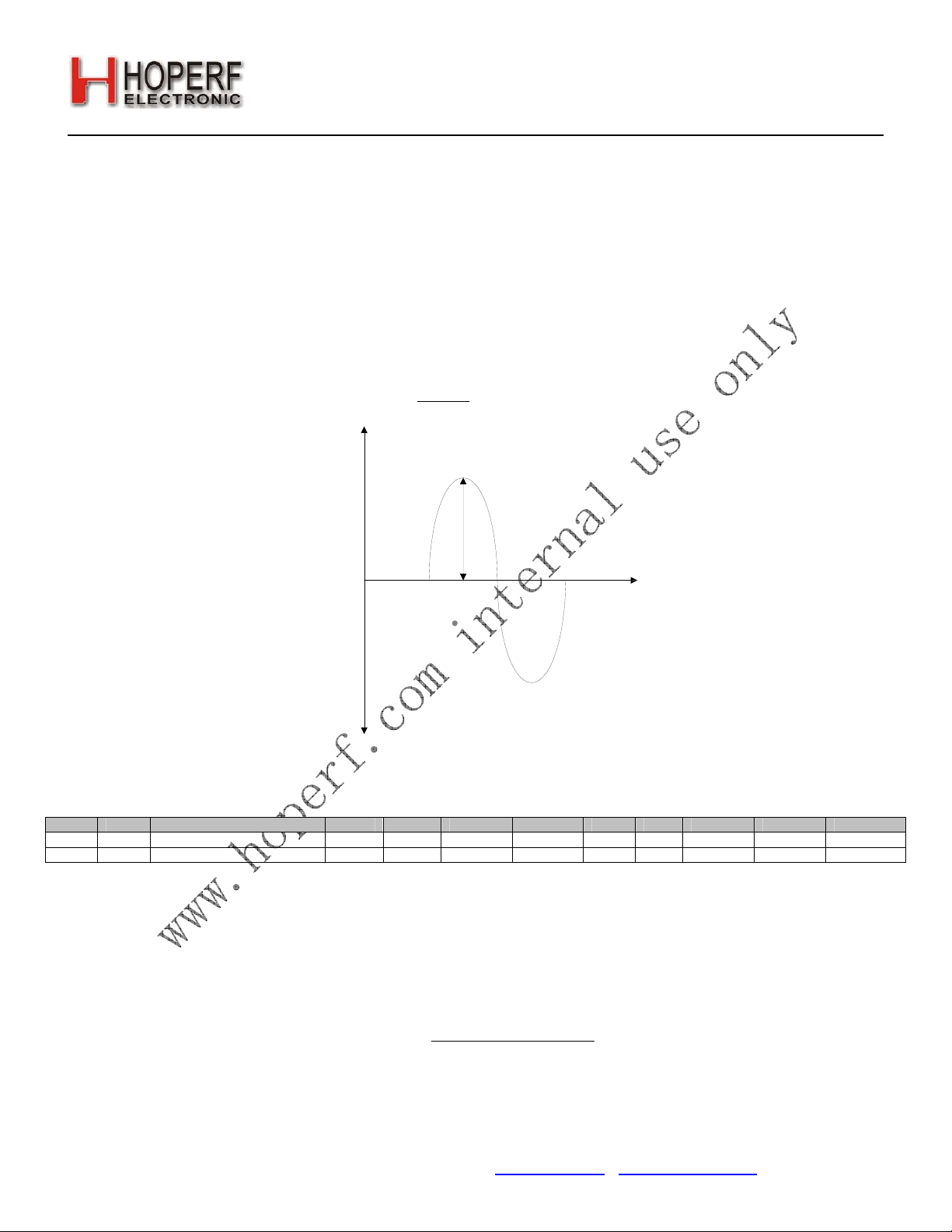
3.2.9.6. Auto Frequency Control (AFC)
The receiver supports automatic frequency control (AFC) to compensate for frequency differences between the
transmitter and receiver reference frequencies. These differences can be caused by the absolute accuracy and
temperature dependencies of the reference crystals. Due to frequency offset compensation in the modem, the receiver
is tolerant to frequency offsets up to 0.25 times the IF bandwidth when the AFC is disabled. When the AFC is enabled,
the received signal will be centered in the pass-band of the IF filter, providing optimal sensitivity and selectivity over a
wider range of frequency offsets up to 0.35 times the IF bandwidth. The trade-off of receiver sensitivity versus carrier
offset and the impact of AFC are illustrated in Figure 9.
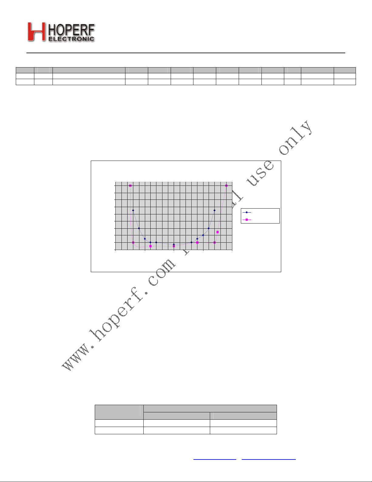
Sensitivity vs Carrier Frequency Offset
(Rb = 100 kHz, Fd = 50 kHz)
-86
-88
-90
-92
-94
-96
-98
-100
RX Sensitivity(dBm)
-102
-104
-100-50050100
Frequency Offset (kHz)
Figure9. Sensitivity vs. Carrier Frequency Offset
The AFC function shares registers 73h and 74h with the Frequency Offset setting. If AFC is enabled, the Frequency
Offset shows the results of the AFC algorithm for the current receive slot. When selecting the preamble length, the
length needs to be long enough to settle the AFC. In general two bytes of preamble is sufficient to settle the AFC.
Disabling the AFC allows the preamble to be shortened. Note that with the AFC disabled, the preamble length must still
be long enough to settle the receiver and to detect the preamble (see "6.7. Preamble Length" on page 45). The AFC
corrects the detected frequency offset by changing the frequency of the Fractional-N PLL. At the end of the preamble
the AFC will freeze. In multi-packet mode the AFC is reset at the end of every packet and will re-acquire the frequency
offset for the next packet. An automatic reset circuit prevents excessive drift by resetting the AFC loop when the tuning
exceeds 2 times the frequency deviation (as set by fd[8:0] in register 71h and 72h) in high band or 1 times the
frequency deviation in low band. This range can be halved by the “afcbd” bit in register 1Dh.
Version: 0.1 Date: 12/23/2008
AFC Disable
AFC Enable
In TX mode the "Register 73h. Frequency Offset 1" is used to provide an offset to the programmed transmit frequency.
This offset allows fine tuning of the transmit frequency to account for the variability of the TX reference frequency. Note
that reading this register shows the frequency offset calculated from the last AFC action not what was previously
written to the Frequency Offset register.
Frequency Correction
RX TX
AFC disabled Freq Offset Register Freq Offset Register
AFC enabled AFC Freq Offset Register
Tel: +86-755-82973805 Fax: +86-755-82973550 E-mail: sales@hoperf.com http://www.hoperf.com
16
Page 17
RF22
[
×
Add R/W Function/Description D7 D6 D5 D4 D3 D2 D1 D0 POR Def.
1D R/W AFC Loop Gearshift
Override
3.2.10. TX Data Rate Generator
The data rate is configurable between 1–128 kbps. For data rates below 30 kbps the ”txdtrtscale” bit in register 70h
should be set to 1. When higher data rates are used this bit should be set to 0.
The TX date rate is determined by the following formula:
The txdr register may be found in the following registers.
Add R/W Function/Description D7 D6 D5 D4 D3 D2 D1 D0 POR Def.
6E R/W TX Data Rate 1 txdr[15] txdr[14] txdr[13] txdr[12] txdr[11] txdr[10] txdr[9] txdr[8] 0Ah
6F R/W TX Data Rate 0 txdr[7] txdr[6] txdr[5] txdr[4] txdr[3] txdr[2] txdr[1] txdr[0] AAh
4. Modulation Options
4.1. Modulation Type
The RF22 supports three different modulation options: Gaussian Frequency Shift Keying (GFSK), Frequency Shift
Keying (FSK), and On-Off Keying (OOK). GFSK is the recommended modulation type as it provides the best
performance and cleanest modulation spectrum. Figure 10 demonstrates the difference between FSK and GFSK for a
Data Rate of 64 kbps. The time domain plots demonstrate the effects of the Gaussian filtering. The frequency domain
plots demonstrate the spectral benefit of GFSK over FSK. The type of modulation is selected with the modtyp[1:0] bits
in "Register 71h. Modulation Mode Control 2". Note that it is also possible to obtain an unmodulated carrier signal by
setting modtyp[1:0] = 00.
modtyp[1:0] Modulation Source
00 Unmodulated Carrier
01 OOK
10 FSK
11 GFSK (enable TX Data CLK when direct mode is used)
afcbd enafc afcgearh[2] afcgearh[1] afcgearh[0] afcgearl[2] afcgearl[1] afcgearl[0] 40h
]
10:15
_
TXDR
[]
txdr
0:15
=
2
=
TXDR
1
⋅+
516
×
2_
MHz
MHztxdr
etxdtrtscal
516 ⋅+
Version: 0.1 Date: 12/23/2008
etxdtrtscal
TX Modulation Time Domain Waveforms -- FSK vs. GFSK
1.5
1.0
0.5
0.0
-0.5
SigData_FSK[0,: :]
-1.0
-1.5
1.0
0.5
0.0
-0.5
SigData_GFSK[0,::]
-1.0
50 100 150 200 250 300 350 400 450 500
0
time, usec
TX Modulation Spectrum -- FSK vs GFSK (Continuous PRBS)
-20
-40
-60
-80
ModSpectrum_FSK
-100
-20
-40
-60
-80
ModSpectrum_GFSK
-100
DataRate TxDev BT_Fi lter
64000.0
32000.0
0 50 100 150 200 250-50-100-150-200-250
freq, KHz
ModIndex
0.5
1.0
Figure10. FSK vs GFSK Spectrums
Tel: +86-755-82973805 Fax: +86-755-82973550 E-mail: sales@hoperf.com http://www.hoperf.com
17
Page 18
RF22
4.2. Modulation Data Source
The RF22 may be configured to obtain its modulation data from one of three different sources: FIFO mode, Direct
Mode, and from a PN9 mode. Furthermore, in Direct Mode, the TX modulation data may be obtained from several
different input pins. These options are set through the dtmod[1:0] field in "Register 71h. Modulation Mode Control 2".
Add R/W Function/Description D7 D6 D5 D4 D3 D2 D1 D0 POR Def.
71 R/W Modulation Mode Control 2 trclk[1] trclk[0] dtmod[1] dtmod[0] eninv fd[8] modtyp[1] modtyp[0] 23h
dtmod[1:0] Modulation Source
00 Direct Mode using TX_Data via GPIO pin (GPIO needs programming accordingly also)
01 Direct Mode using TX_Data via SDI pin (only when nSEL is high)
10 FIFO Mode
11 PN9 (internally generated)
4.3. FIFO Mode
In FIFO mode the integrated FIFOs are used to transmit and receive the data. The FIFOs are accessed via "Register
7Fh. FIFO Access" with burst read/write capability. The FIFOs may be configured specific to the application packet size,
etc. (see "6. Data Handling and Packet Handler" on page 39 for further information). When in FIFO mode the chip will
automatically exit TX or RX State when either the ipksent or ipkvalid interrupt occurs. The chip will return to any of
other states based on the settings in "Register 07h. Operating Mode and Function Control 1". For instance if the chip is
put into TX mode and both the txon and pllon bits are set, the chip will transmit all of the contents of the FIFO and the
ipksent interrupt will occur. When this event occurs the chip will clear the txon bit and return to pllon or Tune Mode. If
no other bits are set in register 07h besides txon initially then the chip will return to the Idle state.
In RX mode the rxon bit will only be cleared if ipkvalid occurs. A CRC, Header, or Sync error will generate an interrupt
and the microcontroller will need to decide on the next action.
Version: 0.1 Date: 12/23/2008
4.4. Direct Mode
For legacy systems that have packet handling within an MCU or other baseband chip, it may not be desirable to use
the FIFO. For this scenario, a Direct Mode is provided which bypasses the FIFOs entirely. In Direct Mode the TX
modulation data is applied to an input pin of the chip and processed in “real time” (i.e., not stored in a register for
transmission at a later time). There are various configurations for choosing which pin is used for the TX Data.
Furthermore, an additional input pin is required for the TX Data Clock if GFSK modulation is desired (only the TX Data
input pin is required for FSK). Two options for the source of the TX Data are available in the dtmod[1:0] field, and
various configurations for the source of the TX Data Clock may be selected through the trclk[1:0] field.
trclk[1:0] TX Data Clock Configuration
00 No TX Clock (only for FSK)
01 TX Data Clock is available via GPIO (GPIO needs programming accordingly as well)
10 TX Data Clock is available via SDO pin (only when nSEL is high)
11 TX Data Clock is available via the nIRQ pin
The eninv bit in Address 71h will invert the TX Data for testing purposes.
4.5. PN9 Mode
In this mode the TX Data is generated internally using a pseudorandom (PN9 sequence) bit generator. The primary
purpose of this mode is for use as a test mode to observe the modulated spectrum without having to load/provide data.
4.6. Synchronous vs. Asynchronous
In Asynchronous mode no clock is used to synchronize the data to the internal modulator. This mode can only be used
with FSK. The advantage of this mode that it saves a microcontroller pin because no data clock is required. The
disadvantage is that you don’t get the clean spectrum and limited BW of GFSK. If Asynchronous FSK is used the
TX_DR register should be set to its maximum value.
Tel: +86-755-82973805 Fax: +86-755-82973550 E-mail: sales@hoperf.com http://www.hoperf.com
18
Page 19
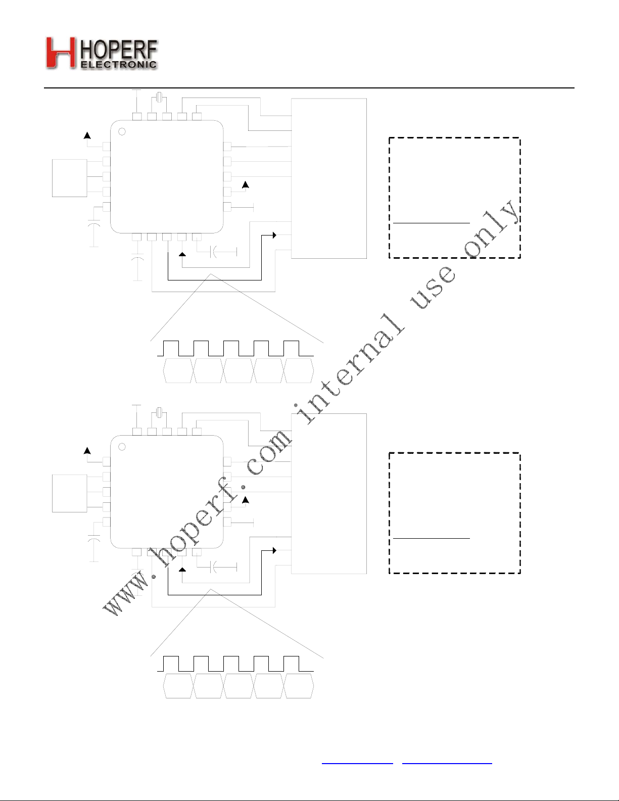
RF22
nIRQ
Matching
VDD_RF
TX
RXp
RXn
VR_IF
DataCLK
XIN
SDN
RF22
ADC_REF
GPIO_0
nIRQ
nSEL
XOUT
SCLK
SDI
SDO
VDD_DIG
GND_DIG
GPIO_1
GPIO_2
VR_DIG
nSEL
SCK
MOSI
MISO
MOD
DATACLK
nRES
Direct synchronous modulation . Full
control over the standard SPI & using
interrupt. Bitrate clock and modulation
u
C
via GPIO's.
GPIO configuration
GP0 : power-on-reset (default)
GP1 : TX DATA clock output
GP2 : TX DATA input
Version: 0.1 Date: 12/23/2008
Matching
MOD(Data)
SDN
VDD_RF
TX
RXp
RXn
VR_IF
RF22
ADC_REF
XIN
GPIO_0
Figure11. Direct Synchronous Mode Example
nIRQ
XOUT
GPIO_1
nIRQ
GPIO_2
nSEL
SCLK
SDI
SDO
VDD_DIG
GND_DIG
VR_DIG
nSEL
SCK
MOSI
MISO
MOD
DATACLK
nRES
uC
Direct asynchronous FSK
modulation. Modulation data
via GPIO2, no data clock
needed in this mode .
GPIO configuration
GP0 : power-on-reset (default)
GP1 : TX DATA clock output
GP2 : TX DATA input
DataCLK
MOD(Data)
Figure 12. Direct Asynchronous Mode Example
Tel: +86-755-82973805 Fax: +86-755-82973550 E-mail: sales@hoperf.com http://www.hoperf.com
19
Page 20
RF22
nIRQ
XIN
Matching
VDD_RF
TX
RXp
RXn
VR_IF
SDN
ADC_REF
GPIO_0
XOUT
GPIO_1
nIRQ
GPIO_2
nSEL
SCLK
SDI
SDO
VDD_DIG
GND_DIG
VR_DIG
Figure13. FIFO Mode Example
5. Internal Functional Blocks
This section provides an overview some of the key blocks of the internal radio architecture.
5.1. RX LNA
The input frequency range for the LNA is 240–930 MHz. The LNA provides gain with a noise figure low enough to
suppress the noise of the following stages. The LNA has one step of gain control which is controlled by the analog gain
control (AGC) algorithm. The AGC algorithm adjusts the gain of the LNA and PGA so the receiver can handle signal
levels from sensitivity to +5 dBm with optimal performance.
5.2. RX I-Q Mixer
The output of the LNA is fed internally to the input of the receive mixer. The receive mixer is implemented as an I-Q
mixer that provides both I and Q channel outputs to the complex IF filter. The mixer consists of two doublebalanced
mixers whose RF inputs are driven in parallel, local oscillator (LO) inputs are driven in quadrature, and separate I and
Q Intermediate Frequency (IF) outputs drive the complex filter. The receive LO signal is supplied by an integrated VCO
and PLL synthesizer operating between 240–930 MHz. The necessary quadrature LO signals are derived from the
divider at the VCO output.
nSEL
SCK
MOSI
MISO
uC
Version: 0.1 Date: 12/23/2008
FIFO mode utilizing internal
packet handler. Data loaded/
read through SPI into FIFO .
GPIO configuration
Not Utilized
5.3. Programmable Gain Amplifier
The Programmable Gain Amplifier (PGA) provides the necessary gain to boost the signal level into the Dynamic Range
of the ADC. The PGA must also have enough gain switching to allow for large input signals to ensure a linear RSSI
range up to –30 dBm. The PGA is designed to have steps of 3 dB which are controlled by the AGC algorithm in the
digital modem.
5.4. ADC
The amplified I&Q IF signals are digitized using an Analog-to-Digital Converter (ADC), which allows for low current
consumption and high dynamic range. The bandpass response of the ADC provides exceptional rejection of out of
band blockers.
5.5. Digital Modem
Using high-performance ADCs allows channel filtering, image rejection, and demodulation to be performed in the
digital domain, resulting in reduced area while increasing flexibility. The digital modem performs the following functions:
Channel Selection Filter
TX Modulation
Tel: +86-755-82973805 Fax: +86-755-82973550 E-mail: sales@hoperf.com http://www.hoperf.com
20
Page 21

RF22
RX Demodulation
AGC
Preamble Detector
Invalid Preamble Detector
Radio Signal Strength Indicator (RSSI)
Automatic Frequency Compensation (AFC)
Packet Handling including EZMacTM features
Cyclic Redundancy Check (CRC)
The digital Channel Filter and Demodulator are optimized for ultra low power consumption and are highly configurable.
Supported modulation types are GFSK, FSK, and OOK. The Channel Filter can be configured to support a large choice
of bandwidths ranging from 620 kHz down to 2.6 kHz. A large variety of data rates are supported ranging from 1 up to
128 kbps. The AGC algorithm is implemented digitally using an advanced control loop optimized for fast response time.
The configurable Preamble Detector is used to improve the reliability of the Sync-word detection. The Sync-word
detector is only enabled when a valid preamble is detected, significantly reducing the probability of false Sync-word
detection.
The Invalid Preamble Detector issues an interrupt when no valid preamble signal is found. After the receiver is enabled,
the Invalid Preamble Detector output is ignored for 16 Tb (Where Tb is the time of a bit duration) to allow the receiver to
settle. The Invalid Preamble Detect interrupt can be used to save power and speed-up search in receive mode. It is
advised to mask the invalid preamble interrupt when Antenna Diversity is enabled.
The Received Signal Strength Indicator (RSSI) provides a measure of the signal strength received on the tuned
channel. The resolution of the RSSI is 0.5 dB. This high resolution RSSI enables accurate channel power
measurements for clear channel assessment (CCA), carrier sense (CS), and listen before talk (LBT) functionality.
Frequency mistuning caused by crystal inaccuracies can be compensated by enabling the digital Automatic Frequency
Control (AFC) in receive mode.
A comprehensive programmable Packet Handler including key features of HopeRFs’ EZMac
variety of communication topologies ranging from peer-to-peer networks to mesh networks. The extensive
programmability of the packet header allows for advanced packet filtering which in turn enables a mix of broadcast,
group, and point-to-point communication.
A wireless communication channel can be corrupted by noise and interference, and it is therefore important to know if
the received data is free of errors. A cyclic redundancy check (CRC) is used to detect the presence of erroneous bits in
each packet. A CRC is computed and appended at the tail of each transmitted packet and verified by the receiver to
confirm that no errors have occurred. The Packet Handler and CRC are extremely valuable features which can
significantly reduce the load on the system microcontroller allowing for a simpler and cheaper microcontroller.
Version: 0.1 Date: 12/23/2008
TM
is integrated to create a
The digital modem includes the TX Modulator which converts the TX Data bits into the corresponding stream of digital
modulation values to be summed with the fractional input to the sigma-delta modulator. This modulation approach
results in highly accurate resolution of the frequency deviation. A Gaussian filter is implemented to support GFSK,
considerably reducing the energy in the adjacent channels. The bandwidth-time product (BT) is 0.5 for all programmed
data rates.
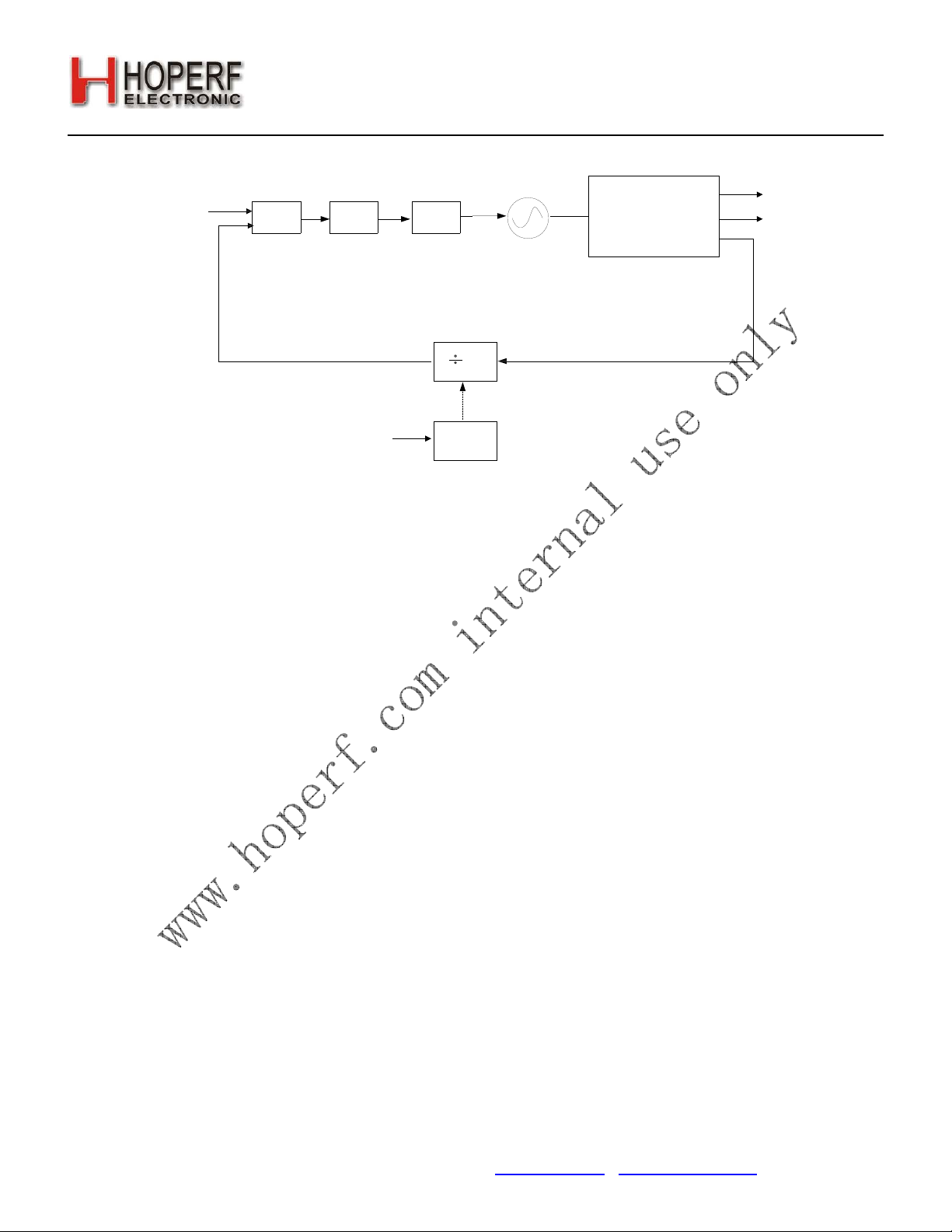
5.6. Synthesizer
An integrated Sigma-Delta (-) Fractional-N PLL synthesizer capable of operating from 240–930 MHz is provided
on-chip. Using a - synthesizer has many advantages; it provides large amounts of flexibility in choosing data rate,
deviation, channel frequency, and channel spacing. The transmit modulation is applied directly to the loop in the digital
domain through the fractional divider which results in very precise accuracy and control over the transmit deviation.
The PLL and -modulator scheme is designed to support any desired frequency and channel spacing in the range
from 240–930 MHz with a frequency resolution of 156.25 Hz (Low band) or 312.5 Hz (High band). The transmit data
Tel: +86-755-82973805 Fax: +86-755-82973550 E-mail: sales@hoperf.com http://www.hoperf.com
21
Page 22
RF22
rate can be programmed between 1–128 kbps, and the frequency deviation can be programmed between ±1–160 kHz.
These parameters may be adjusted via registers as shown in "3.2.9. Frequency Control" on page 26.
Version: 0.1 Date: 12/23/2008
TX
RX
Fref=10M
PFD
CP
TX
Modulation
LPF
Selectable
Divider
VCO
N
Delta-
Sigma
Figure14. PLL Synthesizer Block Diagram
The reference frequency to the PLL is 10 MHz. The PLL utilizes a differential L-C VCO, with integrated on-chip spiral
inductors. The output of the VCO is followed by a configurable divider which will divide down the signal to the desired
output frequency band. The modulus of this divider stage is controlled dynamically by the output from the -
modulator. The tuning resolution of the - modulator is determined largely by the over-sampling rate and the number
of bits carried internally. The tuning resolution is sufficient to tune to the commanded frequency with a maximum
accuracy of 312.5 Hz anywhere in the range between 240–930 MHz.
5.6.1. VCO
The output of the VCO is automatically divided down to the correct output frequency depending on the hbsel and fb[4:0]
fields in "Register 75h. Frequency Band Select". A 2X VCO is utilized to help avoid problems due to frequency pulling,
especially when turning on the integrated Power Amplifier. In receive mode, the LO frequency is automatically shifted
downwards (without reprogramming) by the IF frequency of 937.5 kHz, allowing transmit and receive operation on the
same frequency. The VCO integrates the resonator inductor, tuning varactor, so no external VCO components are
required.
The VCO uses capacitance bank to cover the wide frequency range specified. The capacitance bank will automatically
be calibrated every time the synthesizer is enabled. In certain fast hopping applications this might not be desirable so
the VCO calibration may be skipped by setting the appropriate register.
5.7. Power Amplifier
The RF22 contains an internal integrated power amplifier (PA) capable of transmitting at output levels between +11 to
+20 dBm. The output power is programmable in 3 dB steps through the txpow[1:0] field in "Register 6Dh. TX Power".
The PA design is single-ended and is implemented as a two stage class CE amplifier with efficiency in the range of
45–50% while transmitting at +20 dBm. The efficiency drops to approximately 20% when operating at +11 dBm. Due to
the high efficiency a simple filter is required on the board to filter the harmonics. The PA output is ramped up and down
to prevent unwanted spectral splatter.
5.7.1. Output Power Selection
The output power is configurable in 3 dB steps from +11 dBm to +20 dBm with the txpow[1:0] field in "Register 6Dh. TX
Power". Note that Frequency Hopping (FHSS) is required by the FCC when using an output power level of +20 dBm.
See "8.12. Analog and Digital Test Bus" on page 68 for further information on FHSS. The PA output is ramped up and
Tel: +86-755-82973805 Fax: +86-755-82973550 E-mail: sales@hoperf.com http://www.hoperf.com
22
Page 23
RF22
down to prevent unwanted spectral splatter.
The extra output power can allow use of a cheaper smaller antenna, greatly reducing the overall BOM cost. The higher
power setting of the chip achieves maximum possible range, but of course comes at the cost of higher TX current
consumption. However, depending on the duty cycle of the system the effect on battery life may be insignificant.
Contact HopeRF’s Support for help in evaluating this tradeoff.
Add R/W Function/Description D7 D6 D5 D4 D3 D2 D1 D0 POR Def.
6D R/W TX Power txpow[1] txpow[0] 07h
txpow[1:0] Output Power
00 +11 dBm
01 +14 dBm
10 +17 dBm
11 +20 dBm
5.8. Crystal Oscillator
The RF22 includes an integrated 30 MHz crystal oscillator with a fast start-up time of less than 1 ms. The design is
differential with the required crystal load capacitance integrated on-chip to minimize external components. All that is
required off-chip is the 30 MHz crystal blank.
The crystal load capacitance may be tuned to slightly adjust the frequency of the crystal oscillator. The tuning of the
crystal load capacitance is programmed through the xlc[6:0] field of "Register 09h. 30 MHz Crystal Oscillator Load
Capacitance". The total internal capacitance is 12.5 pF and is adjustable in approximately 127 steps (97fF/step). The
xtalshift bit is a course shift in frequency but is not binary with xlc[6:0]. If AFC is disabled then the synthesizer
frequency may be further adjusted by programming the Frequency Offset field fo[9:0]in "Register 73h. Frequency
Offset 1" and "Register 74h. Frequency Offset 2", as discussed in "3.2.9. Frequency Control" on page 26.
The crystal oscillator frequency is divided down internally and may be output to the microcontroller through one of the
GPIO pins for use as the System Clock. In this fashion, only one crystal oscillator is required for the entire system and
the BOM cost is reduced. The available clock frequencies (i.e., internal division ratios) and the GPIO configuration are
discussed further in "8.2. Microcontroller Clock " on page 54.
The RF22 may also be driven with an external 30 MHz clock signal through the XIN pin.
Add R/W Function/Description D7 D6 D5 D4 D3 D2 D1 D0 POR Def.
09 R/W Crystal Oscillator Load
Capacitance
xtalshift xlc[6] xlc[5 xlc[4] xlc[3] xlc[2] xlc[1] xlc[0] 40h
Version: 0.1 Date: 12/23/2008
5.9. Regulators
There are a total of six regulators integrated onto the RF22. With the exception of the IF and Digital all regulators are
designed to operate with only internal decoupling. The IF and Digital regulators both require an external 1 F
decoupling capacitor. All of the regulators are designed to operate with an input supply voltage from +1.8 to +3.6 V,
and produce a nominal regulated output voltage of +1.7 V ±5%. The internal circuitry nominally operates from this
regulated +1.7 V supply. The output stage of the PA is not connected internally to a regulator and is connected directly
to the battery voltage.
A supply voltage should only be connected to the VDD pins. No voltage should be forced on the IF or DIG regulator
outputs.
6. Data Handling and Packet Handler
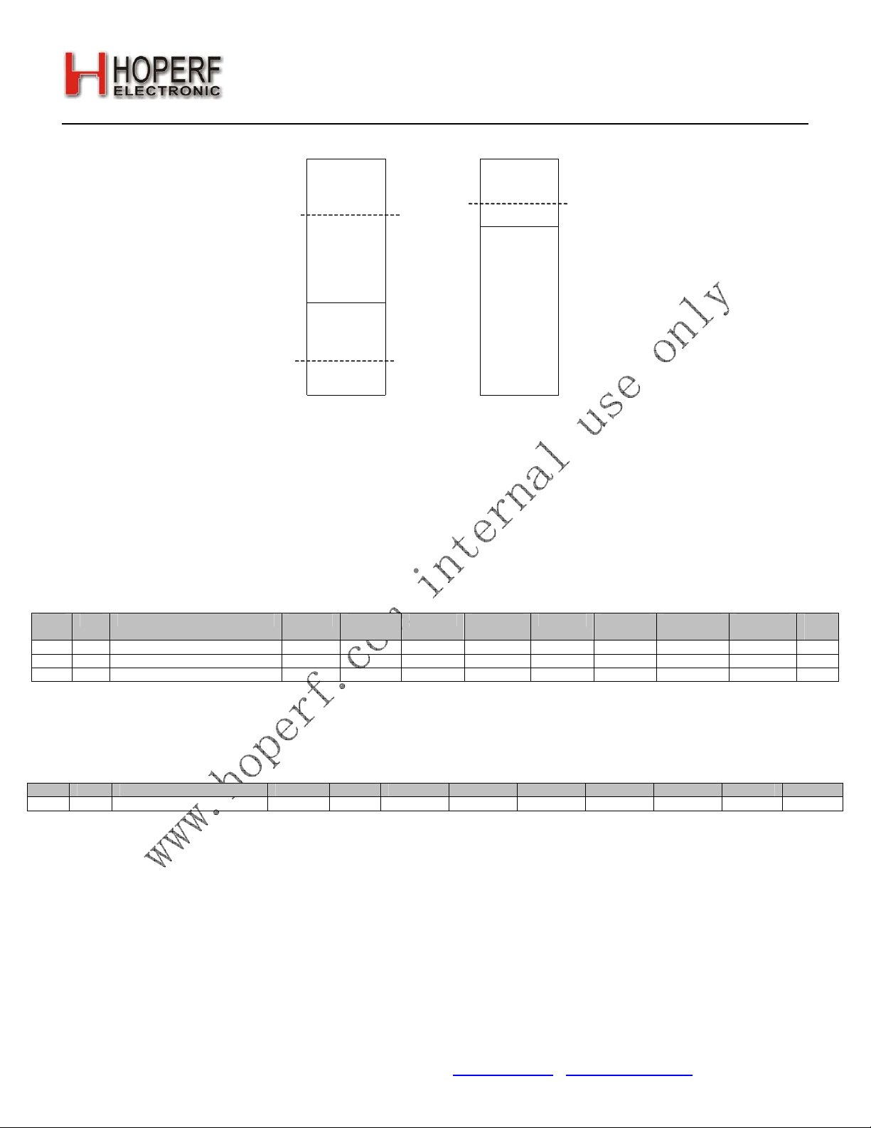
6.1. RX and TX FIFOs
Two 64 byte FIFOs are integrated into the chip, one for RX and one for TX, as shown in Figure 15. "Register 7Fh. FIFO
Access" is used to access both FIFOs. A burst write, as described in "3.1. Serial Peripheral Interface (SPI)" on page 20,
Tel: +86-755-82973805 Fax: +86-755-82973550 E-mail: sales@hoperf.com http://www.hoperf.com
23
Page 24
RF22
to address 7Fh will write data to the TX FIFO. A burst read from address 7Fh will read data from the RX FIFO.
TX FIFORX FIFO
TX FIFO Almost Full
Threshold
TX FIFO Almost Empty
Threshold
Figure15. FIFO Thresholds
The TX FIFO has two programmable thresholds. An interrupt event occurs when the data in the TX FIFO reaches
these thresholds. The first threshold is the FIFO Almost Full threshold, txafthr[5:0]. The value in this register
corresponds to the desired threshold value in number of bytes. When the data being filled into the TX FIFO reaches
this threshold limit, an interrupt to the microcontroller is generated so the chip can enter TX mode to transmit the
contents of the TX FIFO. The second threshold for TX is the FIFO Almost Empty Threshold, txaethr[5:0]. When the
data being shifted out of the TX FIFO reaches the Almost Empty threshold an interrupt will be generated. The
microcontroller will need to switch out of TX mode or fill more data into the TX FIFO. The Transceiver may be
configured so that when the TX FIFO is empty the chip will automatically move to the Ready state. In this mode the TX
FIFO Almost Empty Threshold may not be useful. This functionality is set by the ffidle bit in "Register 08h. Operating
Mode and Function Control 2".
Add R/W Function/Description D7 D6 D5 D4 D3 D2 D1 D0 POR
08 R/W Operating & Function Control 2 antdiv[2] antdiv[1] antdiv[0] rxmpk autotx enldm ffclrrx ffclrtx 00h
7C R/W TX FIFO Control 1 txafthr[5] txafthr[4] txafthr[3] txafthr[2] txafthr[1] txafthr[0] 37h
7D R/W TX FIFO Control 2 txaethr[5] txaethr[4] txaethr[3] txaethr[2] txaethr[1] txaethr[0] 04h
Version: 0.1 Date: 12/23/2008
RX FIFO Almost Full
Threshold
Def.
The RX FIFO has one programmable threshold called the FIFO Almost Full Threshold, rxafthr[5:0]. When the incoming
RX data reaches the Almost Full Threshold an interrupt will be generated to the microcontroller via the nIRQ pin. The
microcontroller will then need to read the data from the RX FIFO.
Add R/W Function/Description D7 D6 D5 D4 D3 D2 D1 D0 POR ef.
7E R/W RX FIFO Control X X rxafthr[5] rxafthr[4] rxafthr[3] rxafthr[2] rxafthr[1] rxafthr[0] 37h
Both the TX and RX FIFO’s may be cleared or reset with the ffclrtx and ffclrrx bits in "Register 08h. Operating Mode
and Function Control 2". All interrupts may be enabled by setting the Interrupt Enabled bits in "Register 05h. Interrupt
Enable 1" and "Register 06h. Interrupt Enable 2". If the interrupts are not enabled the function will not generate an
interrupt on the nIRQ pin but the bits will still be read correctly in the Interrupt Status registers.
6.2. Packet Configuration
When using the FIFOs, automatic packet handling may be enabled for TX mode, RX mode, or both. "Register 71h.
Modulation Mode Control 2" and "Register 30h. Data Access Control" through "Register 49h. Received Header 1"
control the configuration for Packet Handling. The usual fields for network communication (such as preamble,
synchronization word, headers, packet length, and CRC) can be configured to be automatically added to the data
payload. The fields needed for packet generation normally change infrequently and can therefore be stored in registers.
Tel: +86-755-82973805 Fax: +86-755-82973550 E-mail: sales@hoperf.com http://www.hoperf.com
24
Page 25
RF22
"Register 30h. Data Access Control" through "Register 49h. Received Header 1" are used to set the different fields in
the packet structure. Automatically adding these fields to the data payload greatly reduces the amount of
communication between the microcontroller and the RF22 and therefore also reduces the required computational
power of the microcontroller.
The general packet structure is shown in Figure 16. The length of each field is shown below the field. The preamble
pattern is always a series of alternating ones and zeroes, starting with a one. All the fields have programmable lengths
to accommodate different applications. The most common CRC polynominals are available for selection.
Version: 0.1 Date: 12/23/2008
Preamble
1-512 Bytes 1-4 Bytes
Sync Word
TX Header
0-4Byte
Data
Packet Length
0 or 1 Byte
CRC
0 or 2
Bytes
Figure16. Packet Structure
An overview of the packet handler configuration registers is shown in Table 14. A complete register description can be
found in “12.1. Complete Register Table and Descriptions”.
6.3. Packet Handler TX Mode
If the TX packet length is set the packet handler will send the number of bytes in the packet length field before returning
to ready mode and asserting the packet sent interrupt. To resume sending data from the FIFO the microcontroller
needs to command the chip to re-enter TX mode. Figure 17 provides an example transaction where the packet length
is set to three bytes.
1
data
⎫
⎪
This will be send in the first transmission
2
data
⎬
⎪
3
data
⎭
4
data
⎫
data
data
data
data
data
⎪
This will be send in the second transmission
5
⎬
⎪
6
⎭
7
⎫
⎪
This will be send in the third transmission
8
⎬
⎪
9
⎭
Figure17. Multiple Packets in TX Packet Handler
6.4. Packet Handler RX Mode
6.4.1. Packet Handler Disabled
When the packet handler is disabled certain portions of the packet handler are still required. Proper modem operation
requires preamble and sync, as shown in Figure 18. Bits after sync will be treated as raw data with no qualification.
This mode allows for the creation of a custom packet handler when the automatic qualification parameters are not
sufficient. Manchester encoding is supported but the use of data whitening, CRC, or header checks is not.
Preamble
SYNC
DATA
Figure18. Required RX Packet Structure with Packet Handler Disabled
Tel: +86-755-82973805 Fax: +86-755-82973550 E-mail: sales@hoperf.com http://www.hoperf.com
25
Page 26
RF22
6.4.2. Packet Handler Enabled
When the packet handler is enabled, all the fields of the packet structure need to be configured. If multiple packets are
desired to be stored in the FIFO, then there are options available for the different fields that will be stored into the FIFO.
Figure 19 demonstrates the options and settings available when multiple packets are enabled. Figure 20 demonstrates
the operation of fixed packet length and correct/incorrect packets.
Transmission:
Register
Data
Register
Data
rx_multi_pk_en = 0
Header(s)
Length
RX FIFO Contents:
rx_multi_pk_en = 1
txhdlen = 0 txhdlen > 0
Version: 0.1 Date: 12/23/2008
fixpklenfixpklen
0
10 1
Data
FIFO
Data
LL
Data DataData Data
H
H
Figure19. Multiple Packets in RX Packet Handler
Initial state PK 1 OK
RX FIFO Addr.
0
63
Write
Pointer
RX FIFO Addr.
PK 2 OK
Write
Pointer
RX FIFO Addr.
0
H
L
Data
H
L
Data
63
Write
Pointer
0
H
L
Data
63
PK 3
ERROR
RX FIFO Addr.
0
H
L
Data
H
L
Data
H
L
Data
63
Write
Pointer
CRC
error
PK 4 OK
RX FIFO Addr.
0
H
L
Data
H
L
Data
H
L
Data
63
Write
Pointer
Figure20. Multiple Packets in RX with CRC or Header Error
Table13. RX Packet Handler Configuration
Data modes
FIFO_PH 10 1 option set option set option
dtmod[1:0]
FIFO 10 0 option
Direct 0X X set
enpacrx
Direct Data and
CLK IO
Preamble & Sync
word detection
Header Handling
set
—
set
— —
Data Storage in
set
FIFO
CRC Handling
—
Manchester and
option
option
Whitening
Manchester optional for sync-detection
Tel: +86-755-82973805 Fax: +86-755-82973550 E-mail: sales@hoperf.com http://www.hoperf.com
26
Page 27

RF22
Table14. Packet Handler Registers
Addr R/W Function/Description D7 D6 D5 D4 D3 D2 D1 D0 POR Def.
30 R/W Data Access Control enpacrx lsbfrst crcdonly * enpactx encrc crc[1] crc[0] 1Dh
31 R EzMAC status 0 rxcrc1 pksrch pkrx pkvalid crcerror pktx pksent -
32 R/W Header Control 1 enbcast[3] enbcast[2] enbcast[1] enbcast[0] hdch[3] hdch[2] hdch[1] hdch[0] 0Ch
33 R/W Header Control 2
34 R/W Preamble Length prealen[7] prealen[6] prealen[5] prealen[4] prealen[3] prealen[2] prealen[1] prealen[0] 07h
35 R/W Preamble Detection Control preath[4] preath[3] preath[2] preath[1] preath[0] spare spare spare 20h
36 R/W Sync Word 3 sync[31] sync[30] sync[29] sync[28] sync[27] sync[26] sync[25] sync[24] 2Dh
37 R/W Sync Word 2 sync[23] sync[22] sync[21] sync[20] sync[19] sync[18] sync[17] sync[16] D4h
38 R/W Sync Word 1 sync[15] sync[14] sync[13] sync[12] sync[11] sync[10] sync[9] sync[8] 00h
39 R/W Sync Word 0 sync[7] sync[6] sync[5] sync[4] sync[3] sync[2] sync[1] sync[0] 00h
3A R/W Transmit Header 3 txhd[31] txhd[30] txhd[29] txhd[28] txhd[27] txhd[26] txhd[25] txhd[24] 00h
3B R/W Transmit Header 2 txhd[23] txhd[22] txhd[21] txhd[20] txhd[19] txhd[18] txhd[17] txhd[16] 00h
3C R/W Transmit Header 1 txhd[15] txhd[14] txhd[13] txhd[12] txhd[11] txhd[10] txhd[9] txhd[8] 00h
3D R/W Transmit Header 0 txhd[7] txhd[6] txhd[5] txhd[4] txhd[3] txhd[2] txhd[1] txhd[0] 00h
3E R/W Transmit Packet Length pklen[7] pklen[6] pklen[5] pklen[4] pklen[3] pklen[2] pklen[1] pklen[0] 00h
3F R/W Check Header 3 chhd[31] chhd[30] chhd[29] chhd[28] chhd[27] chhd[26] chhd[25] chhd[24] 00h
40 R/W Check Header 2 chhd[23] chhd[22] chhd[21] chhd[20] chhd[19] chhd[18] chhd[17] chhd[16] 00h
41 R/W Check Header 1 chhd[15] chhd[14] chhd[13] chhd[12] chhd[11] chhd[10] chhd[9] chhd[8] 00h
42 R/W Check Header 0 chhd[7] chhd[6] chhd[5] chhd[4] chhd[3] chhd[2] chhd[1] chhd[0] 00h
43 R/W Header Enable 3 hden[31] hden[30] hden[29] hden[28] hden[27] hden[26] hden[25] hden[24] FFh
44 R/W Header Enable 2 hden[23] hden[22] hden[21] hden[20] hden[19] hden[18] hden[17] hden[16] FFh
45 R/W Header Enable 1 hden[15] hden[14] hden[13] hden[12] hden[11] hden[10] hden[9] hden[8] FFh
46 R/W Header Enable 0 hden[7] hden[6] hden[5] hden[4] hden[3] hden[2] hden[1] hden[0] FFh
47 R Received Header 3 rxhd[31] rxhd[30] rxhd[29] rxhd[28] rxhd[27] rxhd[26] rxhd[25] rxhd[24] —
48 R Received Header 2 rxhd[23] rxhd[22] rxhd[21] rxhd[20] rxhd[19] rxhd[18] rxhd[17] rxhd[16] —
49 R Received Header 1 rxhd[15] rxhd[14] rxhd[13] rxhd[12] rxhd[11] rxhd[10] rxhd[9] rxhd[8] —
4A R Received Header 0 rxhd[7] rxhd[6] rxhd[5] rxhd[4] rxhd[3] rxhd[2] rxhd[1] rxhd[0] —
4B R Received Packet Length rxplen[7] rxplen[6] rxplen[5] rxplen[4] rxplen[3] rxplen[2] rxplen[1] rxplen[0] —
hdlen[2] hdlen[1] hdlen[0] fixpklen synclen[1] synclen[0] prealen[8] 22h
Version: 0.1 Date: 12/23/2008
6.5. Data Whitening, Manchester Encoding, and CRC
Data whitening can be used to avoid extended sequences of 0s or 1s in the transmitted data stream to achieve a more
uniform spectrum. When enabled, the payload data bits are XORed with a pseudorandom sequence output from the
built-in PN9 generator. The generator is initialized at the beginning of the payload. The receiver recovers the original
data by repeating this operation. Manchester encoding can be used to ensure a dc-free transmission and good
synchronization properties. When Manchester encoding is used, the effective datarate is unchanged but the actual
datarate (preamble length, etc.) is doubled due to the nature of the encoding. The effective datarate when using
Manchester encoding is limited to 64 kbps. Data Whitening and Manchester encoding can be selected with "Register
70h. Modulation Mode Control 1". The CRC is configured via "Register 30h. Data Access Control".
Tel: +86-755-82973805 Fax: +86-755-82973550 E-mail: sales@hoperf.com http://www.hoperf.com
27
Page 28
RF22
Manchester
Whitening
Version: 0.1 Date: 12/23/2008
CRC (data only = 1)
DATA CRC
Preamble SYNC
HEADER/
ADDRESS
CRC
PK
Length
6.6. Preamble Detector
The RF22 has integrated automatic preamble detection. The preamble length is configurable from 1–256 bytes using
the prealen[7:0] field in "Register 33h. Header Control 2" and "Register 34h. Preamble Length", as described in “6.2.
Packet Configuration”. The preamble detection threshold, preath[4:0] as set in "Register 35h. Preamble Detection
Control 1” is in units of 4 bits. The preamble detector searches for a preamble pattern with a length of preath[4:0].
When a false preamble detect occurs, the receiver will continuing searching for the preamble when no sync word is
detected.
The Preamble Detector output may be programmed onto one of the GPIOs or read in the Interrupt Status registers.
6.7. Preamble Length
The required preamble length threshold will depend on when the receive mode is entered in relation to the transmitted
packet. When the receiver is enabled long before the arrival of the packet, then a short preamble detection threshold
might result in false detects on the received noise before the actual preamble arrives. In this case, it is recommended
to program a 16 or 20 bit detection threshold. When antenna diversity is enabled, it is advised to use the default
preamble detection threshold (16 bit). When the receiver is synchronously enabled just before the start of the packet,
then a shorter preamble detection threshold might be chosen (e.g., 8 bit).
The required preamble length is determined from the sum of the receiver settling time and the preamble detection
threshold. The receiver settling time is listed in Table 15.
Table15. Minimum Receiver Settling Time
Mode
(G)FSK AFC Disabled 1 byte 2 byte 3 byte
(G)FSK AFC Enabled 2 byte 3 byte 4 byte
(G)FSK AFC Disabled +Antenna Diversity
Enabled
(G)FSK AFC Enabled +Antenna Diversity
Enabled
OOK 2 byte 3 byte 4 byte
OOK + Antenna Diversity Enabled 8 byte — 8 byte
Note: The recommended preamble length may be shortened when occasional packet errors are allowed.
Approximate receiver
settling time
1 byte — 7 byte
2 byte — 8 byte
Recommended preamble
length with 8-bit detection
threshold
Recommended preamble
length with 16-bit detection
threshold
6.8. Invalid Preamble Detector
When scanning channels in a Frequency Hopping System, it is desirable to determine if a channel is valid in the
minimum amount of time. The preamble detector can output an invalid preamble detect signal. When an error is
detected in the preamble, the Invalid Preamble Detect signal (nPQD) is asserted, indicating an invalid channel. The
signal can be used to qualify the channel without requiring the full preamble to be received. The Preamble Detect and
Invalid Preamble Detect signals are available in "Register 03h. Interrupt/Status 1" and "Register 04h. Interrupt/ Status
2".
Tel: +86-755-82973805 Fax: +86-755-82973550 E-mail: sales@hoperf.com http://www.hoperf.com
28
Page 29

RF22
The Invalid Preamble Detector issues an interrupt when no valid preamble signal is found. After the receiver is enabled,
the Invalid Preamble Detector will be held low for 16 Tb (Tb is the time of the bit duration) to allow the receiver to settle.
The 16 Tb is a fixed time which will work with a 4-byte Preamble (or longer) when AFC is enabled, or a 3-byte preamble
(or longer) when AFC is disabled. The invalid preamble detect interrupt can be useful to save power and speed-up
search in receive mode.
It is advised to disable the invalid preamble interrupt when Antenna Diversity is enabled. The Invalid Preamble Detect
interrupt may be triggered during the Antenna Diversity algorithm if one of the antennas is weak but the other is
capable of still receiving the signal if the Antenna Diversity algorithm is allowed to complete.
6.9. TX Retransmission and Auto TX
The RF22 is capable of automatically retransmitting the last packet in the FIFO if no additional packets were loaded
into the TX FIFO. Automatic Retransmission is achieved by entering the TX state with the txon bit set. This feature is
useful for Beacon transmission or when retransmission is required due to the absence of a valid acknowledgement.
Only packets that fit completely in the TX FIFO are valid for retransmit. When it is necessary to transmit longer packets,
the TX FIFO uses the circular read/write capability.
An Automatic Transmission is also available. When autotx = 1 the transceiver will enter automatically TX State when
the TX FIFO is almost full. When the TX FIFO is empty the transceiver will automatically return to the IDLE State.
Add R/W Function/Description D7 D6 D5 D4 D3 D2 D1 D0 POR Def.
08 R/W Operating & Function
Control 2
7. RX Modem Configuration
7.1. Modem Settings for FSK and GFSK
The modem performs channel selection and demodulation in the digital domain. The channel filter bandwidth is
configurable from 620 to 2.6 kHz. The data-rate, modulation index, and bandwidth are set via registers 1C–25. The
modulation index is equal to 2 times the peak deviation divided by the data rate (Rb).
Table 16 gives the modem register settings for various common data-rates. Select the desired data-rate (Rb), and
Deviation (Fd) to determine the proper register settings. For data-rates and modulation types not listed in the table a
calculator tool within WDS can be used.
When Manchester coding is disabled, the required channel filter bandwidth is calculated as BW = 2 x (Fd + 0.25Rb)
where Fd is the frequency deviation and Rb is the data rate. For modulation indices below 1 the required channel filter
bandwidth is calculated as BW = Fd + Rb. The channel filter needs to be increased when the frequency offset between
transmitter and receiver is more than half the channel filter bandwidth. In this case it is recommended to enable the
AFC and choose the IF bandwidth equal to 2 x frequency offset.
antdiv[2] antdiv[1] antdiv[0] rxmpk autotx enldm ffclrrx ffclrtx 00h
Version: 0.1 Date: 12/23/2008
Table16. RX Modem Configurations for FSK and GFSK
RX Modem setting examples for GFSK and FSK
Application parameters Register values (hex)
Rb
kbps kHz kHz 1Ch 1Ch 1Ch 20,21h 21,22,23h 24,25h
2 5 5.00 11.5 0 3 3 0FA 08312 06B
2.4 4.8 4.00 11.5 0 3 3 0D0 09D49 0A0
2.4 36 30.00 75.2 0 0 1 683 013A9 005
4.8 4.8 2.00 12.1 0 3 4 068 13A93 278
4.8 45 18.75 95.3 0 0 4 341 02752 00A
9.6 4.8 1.00 18.9 0 2 1 068 13A93 4EE
9.6 45 9.38 95.3 0 0 4 1A1 04EA5 024
10 5 1.00 18.9 0 2 1 064 147AE 521
Fd
mod
index
Tel: +86-755-82973805 Fax: +86-755-82973550 E-mail: sales@hoperf.com http://www.hoperf.com
BW
-3dB
dwn3_bypass ndec_exp[2:0] filset[3:0] rxosr[10:0] ncoff[19:0] crgain[10:0]
29
Page 30

RF22
×
()(
++×
=
×+=
10 40 8.00 90 0 0 3 190 051EC 02B
19.2 9.6 1.00 37.7 0 1 1 068 13A93 4EE
20 10 1.00 37.7 0 1 1 064 147AE 521
20 40 4.00 95.3 0 0 4 0C8 0A3D7 0A6
38.4 19.6 1.02 75.2 0 0 1 068 13A93 4D5
40 20 1.00 75.2 0 0 1 064 147AE 521
40 40 2.00 112.1 0 0 5 064 147AE 291
50 25 1.00 75.2 0 0 1 050 1999A 668
57.6 28.8 1.00 90 0 0 3 045 1D7DC 76E
100 50 1.00 191.5 1 0 F 078 11111 446
100 300 6.00 620.7 1 0 E 078 11111 0B8
125 125 2.00 335.5 1 0 8 060 15555 2AD
7.1.1. Advanced FSK and GFSK Settings
In nearly all cases, the information in Table 16, “RX Modem Configurations for FSK and GFSK,” on page 47 can be
used to determine the required FSK and GFSK modem parameters. The section includes a more detailed discussion of
the various modem parameters to allow for experienced designers to further configure the modem performance.
In FSK or GFSK mode the receiver can handle a wide range of modulation indices ranging from 0.5 up to 32. The
modulation index (h) is defined by the following:
Fd
=
h
When the modulation index is 1 or higher the modulation bandwidth can be approximated by the following equation:
Rb
mod
⎛
⎜
2
⎝
BW 21
2
()
enmanchRb
1
+×
()
×++×= Fdenmanch
Version: 0.1 Date: 12/23/2008
⎞
⎟
⎠
When the modulation index is lower than 1 the modulation bandwidth can be approximated by the following:
)
mod
Where BWmod is an approximation of the modulation bandwidth in kHz, Rb is the payload bit rate in kbps, Fd is the
frequency deviation of the received GFSK/FSK signal in kHz and enmanch is the Manchester Coding parameter (see
Reg. 70h, enmach is 1 when Manchester coding is enabled, enmanch is 0 when disabled).
The bandwidth of the channel select filter in the receiver might need some extra bandwidth to cope with tolerances in
transmit and receive frequencies which depends on the tolerances of the applied crystals. When the relative frequency
error (F
correct the frequency error without needing extra bandwidth. When the frequency error exceeds BW
extra bandwidth will be needed to assure proper AFC operation under worst case conditions. When the AFC is enabled
it is recommended to set the bandwidth of the channel select filter (BW
When the AFC is disabled it is recommended to set the bandwidth of the channel select filter (BWch-sel) according to
the following:
When the required bandwidth (BW) is calculated then the three filter parameters, ndec_exp, dwn3_bypass and filset,
can be found from the table below. When the calculated bandwidth value is not exactly available then select the higher
available bandwidth closest to the calculated bandwidth.
error) between transmitter and receiver is less than half the modulation bandwidth (BWmod) then the AFC will
F
Ferror ×=⇒>
BW
BW
−
1
mod
2
mod
2
mod
selcherror
−
−
2
FdenmanchRbBW
mod/2 then some
ch-sel) according to the formulas below:
BWBW
=⇒≤
2
FBWBW
errorselch
mod
FBW
errorselch
Tel: +86-755-82973805 Fax: +86-755-82973550 E-mail: sales@hoperf.com http://www.hoperf.com
30
Page 31

RF22
Table17. Filter Bandwidth Parameters
BW
[kHz]
2.6 5 0 1 41.7 1 0 2
2.8 5 0 2 45.2 1 0 3
3.1 5 0 3 47.9 1 0 4
3.2 5 0 4 56.2 1 0 5
3.7 5 0 5 64.1 1 0 6
4.2 5 0 6 69.2 1 0 7
4.5 5 0 7 75.2 0 0 1
4.9 4 0 1 83.2 0 0 2
5.4 4 0 2 90.0 0 0 3
5.9 4 0 3 95.3 0 0 4
6.1 4 0 4 112.1 0 0 5
7.2 4 0 5 127.9 0 0 6
8.2 4 0 6 137.9 0 0 7
8.8 4 0 7 142.8 1 1 4
9.5 3 0 1 167.8 1 1 5
10.6 3 0 2 181.1 1 1 9
11.5 3 0 3 191.5 0 1 15
12.1 3 0 4 225.1 0 1 1
14.2 3 0 5 248.8 0 1 2
16.2 3 0 6
17.5 3 0 7 284.9 0 1 4
18.9 2 0 1 335.5 0 1 8
21.0 2 0 2 361.8 0 1 9
22.7 2 0 3 420.2 0 1 10
24.0 2 0 4 468.4 0 1 11
28.2 2 0 5 518.8 0 1 12
32.2 2 0 6 577.0 0 1 13
34.7 2 0 7 620.7 0 1 14
37.7 1 0 1
7.2. Modem Settings for OOK
The RF22 is configured for OOK mode by setting the modtyp[1:0] field to OOK in "Register 71h. Modulation Mode
Control 2". In OOK mode, the following parameters can be configured: data rate, manchester coding, channel filter
bandwidth, and the clock recovery oversampling rate.
The required data rate (Rb) is configured via the txdr[15:0] field in "Register 6Eh. TX Data Rate 1" and "Register 6Fh.
TX Data Rate 0". For data rates < 30 kbps, “txdtrscale” in "Register 70h. Modulation Mode Control 1" should be set to 1
for increased data rate precision. Manchester coding is enabled by setting enmanch in Register 70h. The receive
channel select filter bandwidth is configured via "Register 1Ch. IF Filter Bandwidth". The register settings for the
available channel bandwidth settings are shown in Table 18.
ndec_exp
1C-[6:4]
dwn3_bypass
1C-[7]
filset
1C-[3:0]
BW
[kHz]
269.3 0 1 3
ndec_exp
1C-[6:4]
Table18. Channel Filter Bandwidth Settings
BW[kHz] dwn3_bypass filset[3:0]
75.2 0 1
83.2 0 2
90 0 3
95.3 0 4
112.1 0 5
127.9 0 6
137.9 0 7
191.5 1 F
225.1 1 1
248.8 1 2
269.3 1 3
284.9 1 4
335.5 1 8
361.8 1 9
420.2 1 10
Version: 0.1 Date: 12/23/2008
dwn3_bypass
1C-[7]
filset
1C-[3:0]
Tel: +86-755-82973805 Fax: +86-755-82973550 E-mail: sales@hoperf.com http://www.hoperf.com
31
Page 32

RF22
(
×+×
(
468.4 1 11
518.8 1 12
577 1 13
620.7 1 14
The proper settings for ndec[2:0] are listed in Table 19 where Rb is the data rate (Rb) which is doubled when
Manchester coding is enabled.
Table19. ndec[2:0] Settings
Rb(1+ enmanch) [kbps]
Min Max
0 1 5
1 2 4
2 3 3
3 8 2
8 40 1
40 65 0
The clock recovery oversampling rate is set via rxosr[10:0] in "Register 20h. Clock Recovery Oversampling Rate" and
"Register 21h. Clock Recovery Offset 2". ndec_exp and dwn3_bypass together with the receive data rate (Rb) are
used to calculate rxosr:
rxosr
=
ndec
−
3exp_
ndec[2:0]
bypassdwn
_321500
()
enmanchRb
+××
12
Version: 0.1 Date: 12/23/2008
)
Where: Rb is in kbps and enmanch is the Manchester Coding parameter. The resulting rxdr[10:0] value should be
rounded to an integer hexadecimal number.
The clock recovery offset ncoff[19:0] in "Register 21h. Clock Recovery Offset 2", "Register 22h. Clock Recovery Offset
1", and "Register 23h. Clock Recovery Offset 0" is calculated as follows:
ndec
exp_20
+
ncoff
=
enmanchRb
()
Where: Rb is in kbps.
The clock recovery gain crgain[10:0] in "Register 24h. Clock Recovery Timing Loop Gain 1" and "Register 25h. Clock
Recovery Timing Loop Gain 0" is calculated as follows:
crgain
2+=
)
21
×+×
bypassdwn
×+×
_321500
16
2
rxosr
Table20. RX Modem Configuration for OOK with Manchester Disabled
Appl Parameters
Rb RX BW dwn3_bypass ndec_exp[2:0] filset[3:0] rxosr[10:0] ncoff[19:0] crgain[10:0]
[kbps] [kHz] 1Ch 1Ch 1Ch 20,21h 21,22,23h 24,25h
1.2 75 0 4 1 0D0 09D49 13D
1.2 110 0 4 5 0D0 09D49 13D
1.2 335 1 4 8 271 0346E 06B
1.2 420 1 4 A 271 0346E 06B
1.2 620 1 4 E 271 0346E 06B
2.4 335 1 3 8 271 0346E 06B
4.8 335 1 2 8 271 0346E 06B
9.6 335 1 1 8 271 0346E 06B
10 335 1 1 8 258 0369D 06F
15 335 1 1 8 190 051EC 0A6
RX Modem Setting Examples for OOK (Manchester Disabled)
Register Values
Tel: +86-755-82973805 Fax: +86-755-82973550 E-mail: sales@hoperf.com http://www.hoperf.com
32
Page 33

RF22
19.2 335 1 1 8 139 068DC 0D3
20 335 1 1 8 12C 06D3A 0DC
30 335 1 1 8 0C8 0A3D7 14A
38.4 335 1 1 8 09C 0D1B7 1A6
40 335 1 1 8 096 0DA74 1B7
Table21. RX Modem Configuration for OOK with Manchester Enabled
Appl Parameters
Rb RX BW dwn3_bypass ndec_exp[2:0] filset[3:0] rxosr[10:0] ncoff[19:0] crgain[10:0]
[kbps] [kHz] 1Ch 1Ch 1Ch 20,21h 21,22,23h 24,25h
1.2 75 0 3 1 0D0 04EA5 13D
1.2 110 0 3 5 0D0 04EA5 13D
1.2 335 1 3 8 271 01A37 06B
1.2 420 1 3 A 271 01A37 06B
1.2 620 1 3 E 271 01A37 06B
2.4 335 1 2 8 271 01A37 06B
4.8 335 1 1 8 271 01A37 06B
9.6 335 1 1 8 139 0346E 0D3
10 335 1 1 8 12C 0369D 0DC
15 335 1 1 8 0C8 051EC 14A
19.2 335 1 1 8 09C 068DC 1A6
20 335 1 1 8 096 06D3A 1B7
30 335 1 0 8 0C8 051EC 14A
38.4 335 1 0 8 09C 068DC 1A6
40 335 1 0 8 096 06D3A 1B7
8. Auxiliary Functions
8.1. Smart Reset
The RF22 contains an enhanced integrated SMART RESET or POR circuit. The POR circuit contains both a classic
level threshold reset as well as a slope detector POR. This reset circuit was designed to produce reliable reset signal in
any circumstances. Reset will be initiated if any of the following conditions occur:
Initial power on, when VDD starts from 0V: reset is active till VDD reaches VRR (see table);
z
When VDD decreases below VLD for any reason: reset is active till VDD reaches VRR again;
z
z A software reset via "Register 08h. Operating Mode and Function Control 2": reset is active for time T
z On the rising edge of a VDD glitch when the supply voltage exceeds the following time functioned limit:
RX Modem Setting Examples for OOK (Manchester Enabled)
Register Values
VDD nom.
Version: 0.1 Date: 12/23/2008
SWRST
VDD(t)
reset limit:
0.4V+t*0.2V/ms
0.4V
actual VDD(t)
showing glitch
Reset
T
P
t=0,
VDD starts to rise
reset:
Vglitch>=0.4+t*0.2V/ms
Figure 22. POR Glitch Parameters
Tel: +86-755-82973805 Fax: +86-755-82973550 E-mail: sales@hoperf.com http://www.hoperf.com
t
33
Page 34

RF22
Table22. POR Parameters
Parameter Symbol Comment Min Typ Max Unit
Release Reset Voltage VRR 0.85 1.3 1.75 V
Power-On VDD Slope S
Low VDD Limit VLD VLD<VRR is guaranteed 0.7 1 1.3 V
Software Reset Pulse T
Threshold Voltage V
Reference Slope K 0.2 V/ms
VDD Glitch Reset Pulse TP Also occurs after SDN, and initial power on 5 15 40 ms
The reset will initialize all registers to their default values. The reset signal is also available for output and use by the
microcontroller by using the default setting for GPIO_0. The inverted reset signal is available by default on GPIO_1.
8.2. Microcontroller Clock
The crystal oscillator frequency is divided down internally and may be output to the microcontroller through GPIO2.This
feature is useful to lower BOM cost by using only one crystal in the system. The system clock frequency is selectable
from one of 8 options, as shown below. Except for the 32.768 kHz option, all other frequencies are derived by dividing
the Crystal Oscillator frequency. The 32.768 kHz clock signal is derived from an internal RC Oscillator or an external 32
kHz Crystal, depending on which is selected. The GPIO2 default is the microcontroller clock with a 1 MHz
microcontroller clock output.
Add R/W Function/Description D7 D6 D5 D4 D3 D2 D1 D0 POR Def.
0A R/W Microcontroller Output Clock clkt[1] clkt[0] enlfc mclk[2] mclk[1] mclk[0] 0Bh
tested VDD slope region 0.03 300 V/ms
VDD
50 470 us
SWRST
0.4 V
TSD
Version: 0.1 Date: 12/23/2008
mclk[2:0] Modulation Source mclk[2:0] Modulation Source
000 30 MHz 100 3 MHz
001 15 MHz 101 2 MHz
010 10 MHz 110 1 MHz
011 4 MHz 111 32.768 kHz
If the microcontroller clock option is being used there may be the need of a System Clock for the microcontroller while
the RF22 is in SLEEP mode. Since the Crystal Oscillator is disabled in SLEEP mode in order to save current, the
low-power 32.768 kHz clock can be automatically switched to become the microcontroller clock. This feature is called
Enable Low Frequency Clock and is enabled by the enlfc bit. When enlfc = 1 and the chip is in SLEEP mode then the
32.768 kHz clock will be provided to the microcontroller as the System Clock, regardless of the setting of mclk[2:0]. For
example, if mclk[2:0] = 000, 30 MHz will be provided through the GPIO output pin to the microcontroller as the System
Clock in all IDLE, TX, or RX states. When the chip is commanded to SLEEP mode, the System Clock will become
32.768 kHz.
Another available feature for the microcontroller clock is the Clock Tail, clkt[1:0]. If the Enable Low Frequency Clock
feature is not enabled (enlfc = 0), then the System Clock to the microcontroller is disabled in SLEEP mode. However, it
may be useful to provide a few extra cycles for the microcontroller to complete its operation prior to the shutdown of the
System Clock signal. Setting the clkt[1:0] field will provide additional cycles of the System Clock before it shuts off.
clkt[1:0] Modulation Source
00 0 cycles
01 128 cycles
10 256 cycles
11 512 cycles
If an interrupt is triggered, the microcontroller clock will remain enabled regardless of the selected mode. As soon as
the interrupt is read the state machine will then move to the selected mode. For instance, if the chip is commanded to
Sleep mode but an interrupt has occurred the 30 MHz XTAL will not disable until the interrupt has been cleared.
Tel: +86-755-82973805 Fax: +86-755-82973550 E-mail: sales@hoperf.com http://www.hoperf.com
34
Page 35

RF22
8.3. General Purpose ADC
An 8-bit SAR ADC is integrated onto the chip for general purpose use, as well as for digitizing the temperature sensor
reading. “Register 0Fh. ADC Configuration,” on page 56 must be configured depending on the use of the GP ADC
before use. The architecture of the ADC is demonstrated in Figure 23. First the input of the ADC must be selected by
setting the ADCSEL[2:0] depending on the use of the ADC. For instance, if the ADC is going to be used to read out the
internal temperature sensor, then ADCSEL[2:0] should be set to 000. Next, the input reference voltage to the ADC
must be chosen. By default, the ADC uses the bandgap voltage as a reference so the input range of the ADC is from
0–1.02 V with an LSB resolution of 4 mV (1.02/255). Changing the ADC reference will change the LSB resolution
accordingly.
Every time the ADC conversion is desired, the ADCStart bit in "Register 0Fh. ADC Configuration" must be set to 1. This
is a self clearing bit that will be cleared at the end of the conversion cycle of the ADC. The conversion time for the ADC
is 350 us. After the 350 us or when the ADCstart/busy bit is cleared, then the ADC value may be read out of "Register
11h. ADC Value". Setting the "Register 10h. ADC Sensor Amplifier Offset", ADC Sensor Amplifier Offset is only
necessary when the ADC is configured to used as a Bridge Sensor as described in the following section.
GPIO0
GPIO1
GPIO2
TS
VBG(1.2V)
Diff. MUX
…………
ADCSEL<2:0>
Diff. Amp.
OTR<3:0>
VBAT/3
VBAT/2
GAIN<1:0>
Input MUX
……
ADCSEL<2:0>
Ref MUX
……
Vin
Vref
Version: 0.1 Date: 12/23/2008
8-bit ADC
VMEAS<7:0>
0-1020mV / 0-255
REFSEL<1:0>
Figure 23. General Purpose ADC Architecture
Add R/W Function/Description D7 D6 D5 D4 D3 D2 D1 D0
0F R/W ADC Configuration adcstart/adcbusy adcsel[2] adcsel[1] adcsel[0] adcref[1] adcref[0] adcgain[1] adcgain[0] 00h
10 R/W ADC Sensor Amplifier
Offset
11 R ADC Value adc[7] adc[6] adc[5] adc[4] adc[3] adc[2] adc[1] adc[0] —
adcoffs[3] adcoffs[2] adcoffs[1] adcoffs[0] 00h
POR
Def.
Register 0Fh. ADC Configuration
Bit D7 D6 D5 D4 D3 D2 D1 D0
Name
Type R/W
Reset value = 00000000
Bit Name Function
7
6:4 adcsel[2:0] ADC Input Source Selection.
adcstart/adcdone
adcstart/adcdone
Tel: +86-755-82973805 Fax: +86-755-82973550 E-mail: sales@hoperf.com http://www.hoperf.com
adcsel[2:0] adcref[1:0]
R/W
ADC Measurement Start Bit.
Reading this bit gives 0 if the ADC measurement cycle has been finished.
R/W
adcgain[1:0]
R/W
35
Page 36

RF22
The internal 8 bit ADC input source can be selected as follows:
000: Internal Temperature Sensor
001: GPIO0, single-ended
010: GPIO1, single-ended
011: GPIO2, single-ended
100: GPIO0(+) – GPIO1(–), differential
101: GPIO1(+) – GPIO2(–), differential
110: GPIO0(+) – GPIO2(–), differential
111: GND
3:2 adcref[1:0] ADC Reference Voltage Selection.
The reference voltage of the internal 8 bit ADC can be selected as follows:
0X: bandgap voltage (1.2V)
10: VDD / 3
11: VDD / 2
1:0 adcgain[1:0] ADC Sensor Amplifier Gain Selection.
8.3.1. ADC Differential Input Mode—Bridge Sensor Example
The differential input mode of ADC8 is designed to directly interface any bridge-type sensor, which is demonstrated in
the figure below. As seen in the figure the use of the ADC in this configuration will utilize two GPIO pins. The supply
source of the bridge and chip should be the same to eliminate the measuring error caused by battery discharging. For
proper operation one of the VDD dependent references (VDD/2 or VDD/3) should be selected for the reference voltage
of ADC8. VDD/2 reference should be selected for VDD lower than 2.7 V, VDD/3 reference should be selected for VDD
higher than 2.7 V. The differential input mode supports programmable gain to match the input range of ADC8 to the
characteristic of the sensor and VDD proportional programmable offset adjustment to compensate the offset of the
sensor.
Microcontroller
Version: 0.1 Date: 12/23/2008
RF22
VDD
+ -
GPIO2
GPIO1
Digital I/O
GND
measure control
GND
Figure24. ADC Differential Input Example—Bridge Sensor
The adcgain[1:0] bits in "Register 0Eh. I/O Port Configuration" determine the gain of the differential/single ended
amplifier. This is used to fit the input range of the ADC8 to bridge sensors having different sensitivity:
adcgain[1] adcgain[0]
0 0 22/13 33/13 16.7
0 1 44/13 66/13 8.4
1 0 66/13 99/13 5.6
1 1 88/13 132/13 4.2
adcref[0] = 0 adcref[0] = 1
Differential Gain
Input Range (% of VDD)
Note: The input range is the differential voltage measured between the selected GPIO pins corresponding to the full ADC range
(255).
Tel: +86-755-82973805 Fax: +86-755-82973550 E-mail: sales@hoperf.com http://www.hoperf.com
36
Page 37

RF22
The gain is different for different VDD dependent references so the reference change has no influence on input range and digital
measured values.
The differential offset can be coarse compensated by the adcoffs[3:0] bits found in "Register 11h. ADC Value". Fine
compensation should be done by the microcontroller software. The main reason for the offset compensation is to shift
the negative offset voltage of the bridge sensor to the positive differential voltage range. This is essential as the
differential input mode is unipolar. The offset compensation is VDD proportional, so the VDD change has no influence
on the measured value.
adcoffs[3] Input Offset (% of VDD)
0
1 adcoffs[2:0] x 0.12
Input Offset
0.84 %
0 %
1
0 15
0 if adcoffs[2:0] = 0
–(8 – adcoffs[2:0]) x 0.12
8
Version: 0.1 Date: 12/23/2008
adcoffs[3:0]
0.84 %
Figure25. ADC Differential Input Offset for Sensor Offset Coarse Compensation
8.4. Temperature Sensor
An analog temperature sensor is integrated into the chip. The temperature sensor will be automatically enabled when
the temperature sensor is selected as the input of the ADC or when the analog temp voltage is selected on the analog
test bus. The temperature sensor value may be digitized using the general-purpose ADC and read out over the SPI
through "Register 10h. ADC Sensor Amplifier Offset". The range of the temperature sensor is selectable to configure to
the desired application and performance. The table below demonstrates the settings for the different temperature
ranges and performance. To use the Temp Sensor:
1. Set input for ADC to be Temperature Sensor, "Register 0Fh. ADC Configuration"—adcsel[2:0] = 000
2. Set Reference for ADC, "Register 0Fh. ADC Configuration"—adcref[1:0] = 00
3. Set Temperature Range for ADC, "Register 12h. Temperature Sensor Calibration"—tsrange[1:0]
4. Set entsoffs = 1, "Register 12h. Temperature Sensor Calibration"
5. Trigger ADC Reading, "Register 0Fh. ADC Configuration"—adcstart = 1
6. Read-out Value—Read Address in "Register 11h. ADC Value"
Add R/W Function/Description D7 D6 D5 D4 D3 D2 D1 D0
12 R/W
Temperature Sensor
Control
tsrange[1] tsrange[0] entsoffs entstrim vbgtrim[3] vbgtrim[2] vbgtrim[1] vbgtrim[0] 20h
POR
Def.
13 R/W
Temperature Value
Offset
Tel: +86-755-82973805 Fax: +86-755-82973550 E-mail: sales@hoperf.com http://www.hoperf.com
tvoffs[7] tvoffs[6] tvoffs[5] tvoffs[4] tvoffs[3] tvoffs[2] tvoffs[1] tvoffs[0] 00h
37
Page 38

RF22
Bit D7 D6 D5 D4 D3 D2 D1 D0
Name tsrange[1:0] entoff envbgcal vbgcal[3:0]
Type R/W R/W R/W R/W
Reset value = 00100000
Bit Name Function
7:6 tsrange[1:0] Temperature Sensor Range Selection.
5 entoff Temperature Sensor Offset Enable.
4 envbgcal Temperature Sensor Calibration Enable.
3:0 vbgcal[3:0] Temperature Sensor Calibration Value.
entoff tsrange[1] tsrange[0] Temp. range Unit Slope ADC8 LSB
1 0 0 –64 … 64 °C 8 mV/°C 0.5 °C
1 0 1 –64 … 192 °C 4 mV/°C 1 °C
1 1 0 0 … 128 °C 8 mV/°C 0.5 °C
1 1 1 –40 … 216 °F 4 mV/°F 1 °F
0* 1 0 0 … 341 °K 3 mV/°K 1.333 °K
*Note: Absolute temperature mode, no temperature shift. This mode is only for test purposes. POR value of EN_TOFF is 1.
(FS range is 0..1024 mV)
o
00: –64
C~64oC (full operating range), with 0.5 oC resolution (1 LSB in the 8 bit ADC)
o
C ~192oC, with 1oC resolution (1 LSB in the 8 bit ADC)
01: –64
o
11: 0
C~128oC, with 0.5oC resolution (1 LSB in the 8 bit ADC)
o
10: –40
F~216oF, with 1oF resolution (1 LSB in the 8 bit ADC)
Table23. Temperature Sensor Range
Version: 0.1 Date: 12/23/2008
Control to adjust the temperature sensor accuracy is available by adjusting the bandgap voltage. By enabling the
envbgcal and using the vbgcal[3:0] bits to trim the bandgap the temperature sensor accuracy may be fine tuned in the
final application. The slope of the temperature sensor is very linear and monotonic but the exact accuracy or offset in
temperature is difficult to control better than ±10 °C. With the vbgtrim or bandgap trim though the initial temperature
offset can be easily adjusted and be better than ±3 °C.
The different ranges for the temperature sensor and ADC8 are demonstrated in Figure 26. The value of the ADC8 may
be translated to a temperature reading by ADC8Value x ADC8 LSB + Lowest Temperature in Temp Range. For
instance for a tsrange = 00, Temp = ADC8Value x 0.5 – 64.
Temperature Measurement with ADC8
300
250
200
150
ADC value
100
50
0
-40
Temperature [Celsius]
40 60
80 100200-20
Sensor Range 0
Sensor Range 1
Sensor Range 2
Sensor Range 3
Figure26. Temperature Ranges using ADC8
Tel: +86-755-82973805 Fax: +86-755-82973550 E-mail: sales@hoperf.com http://www.hoperf.com
38
Page 39

RF22
×+=
8.5. Low Battery Detector
A low battery detector (LBD) with digital read-out is integrated into the chip. A digital threshold may be programmed
into the lbdt[4:0] field in "Register 1Ah. Low Battery Detector Threshold". When the digitized battery voltage reaches
this threshold an interrupt will be generated on the nIRQ pin to the microcontroller. The microcontroller will then need to
verify the interrupt by reading "Register 03h. Interrupt/Status 1" and "Register 04h. Interrupt/Status 2". If the LBD is
enabled while the chip is in SLEEP mode, it will automatically enable the RC oscillator which will periodically turn on
the LBD circuit to measure the battery voltage. The battery voltage may also be read out through "Register 1Bh.
Battery Voltage Level" at any time when the LBD is enabled. The Low Battery Detect function is enabled by setting
enlbd=1 in "Register 07h. Operating Mode and Function Control 1".
Ad R/W Function/Description D7 D6 D5 D4 D3 D2 D1 D0 POR Def.
1A R/W Low Battery Detector Threshold lbdt[4] lbdt[3] lbdt[2] lbdt[1] lbdt[0] 14h
1B R Battery Voltage Level 0 0 0 vbat[4] vbat[3] vbat[2] vbat[1] vbat[0] —
The LBD output is digitized by a 5-bit ADC. When the LBD function is enabled, enlbd = 1 in "Register 07h. Operating
Mode and Function Control 1", the battery voltage may be read at anytime by reading "Register 1Bh. Battery Voltage
Level". A Battery Voltage Threshold may be programmed to register 1Ah. When the battery voltage level drops below
the battery voltage threshold an interrupt will be generated on nIRQ pin to the microcontroller if the LBD interrupt is
enabled in "Register 06h. Interrupt Enable 2". The microcontroller will then need to verify the interrupt by reading the
interrupt status register, Addresses 03 and 04H. The LSB step size for the LBD ADC is 50 mV, with the ADC range
demonstrated in the table below. If the LBD is enabled the LBD and ADC will automatically be enabled every 1 s for
approximately 250 s to measure the voltage which minimizes the current consumption in Sensor mode. Before an
interrupt is activated four consecutive readings are required.
507.1
ADCValuemVtageBatteryVol
Version: 0.1 Date: 12/23/2008
ADC Value VDD Voltage [V]
0 < 1.7
1 1.7–1.75
2 1.75–1.8
… …
29 3.1–3.15
30 3.15–3.2
31 > 3.2
8.6. Wake-Up Timer
The chip contains an integrated wake-up timer which periodically wakes the chip from SLEEP mode. The wake-up
timer runs from the internal 32.768 kHz RC Oscillator. The wake-up timer can be configured to run when in SLEEP
mode. If enwt = 1 in "Register 07h. Operating Mode and Function Control 1" when entering SLEEP mode, the wake-up
timer will count for a time specified by the Wake-Up Timer Period in Registers 10h-12h. At the expiration of this period
an interrupt will be generated on the nIRQ pin if this interrupt is enabled. The microcontroller will then need to verify the
interrupt by reading the Interrupt Status Registers 03h-04h. The wake-up timer value may be read at any time by the
wtv[15:0] read only registers 13h-14h.
The formula for calculating the Wake-Up Period is the following:
DR
−
××
M
WUT
=
232
ms
768.32
WUT Register Description
wtr[3:0] R Value in Formula
wtd[1:0] D Value in Formula
wtm[15:0] M Value in Formula
Tel: +86-755-82973805 Fax: +86-755-82973550 E-mail: sales@hoperf.com http://www.hoperf.com
39
Page 40

RF22
Use of the D variable in the formula is only necessary if finer resolution is required than the R value gives.
Add R/W Function/Description D7 D6 D5 D4 D3 D2 D1 D0 POR Def.
14 R/W Wake-Up Timer Period 1 wtr[3] wtr[2] wtr[1] wtr[0] wtd[1] wtd[0] 00h
15 R/W Wake-Up Timer Period 2 wtm[15] wtm[14] wtm[13] wtm[12] wtm[11] wtm[10] wtm[9] wtm[8] 00h
16 R/W Wake-Up Timer Period 3 wtm[7] wtm[6] wtm[5] wtm[4] wtm[3] wtm[2] wtm[1] wtm[0] 00h
17 R Wake-Up Timer Value 1 wtv[15] wtv[14] wtv[13] wtv[12] wtv[11] wtv[10] wtv[9] wtv[8] —
18 R Wake-Up Timer Value 2 wtv[7] wtv[6] wtv[5] wtv[4] wtv[3] wtv[2] wtv[1] wtv[0] —
There are two different methods for utilizing the wake-up timer (WUT) depending on if the WUT interrupt is enabled in
"Register 06h. Interrupt Enable 2". If the WUT interrupt is enabled then nIRQ pin will go low when the timer expires.
The chip will also change state so that the 30M XTAL is enabled so that the microcontroller clock output is available for
the microcontroller to use process the interrupt. The other method of use is to not enable the WUT interrupt and use
the WUT GPIO setting. In this mode of operation the chip will not change state until commanded by the microcontroller.
The two different modes of operation of the WUT are demonstrated in Figure 27.
A 32 kHz XTAL may also be used for better timing accuracy. By setting the x32ksel bit in 07h, GPIO0 is automatically
reconfigured so that an external 32 kHz XTAL may be connected to this pin. In this mode, the GPIO0 is extremely
sensitive to parasitic capacitance, so only the XTAL should be connected to this pin and the XTAL should be physically
located as close to the pin as possible. Once the x32ksel bit is set, all internal functions such as WUT, micro-controller
clock, and LDC mode will use the 32K XTAL and not the 32 kHz RC oscillator.
WUT Period
GPIOX=00001
Interrupt Enable enwut=1 (Reg 06h)
Version: 0.1 Date: 12/23/2008
nIRQ
SPI Interrupt
Read
Chip State
Sleep Ready Sleep Ready Sleep Ready Sleep
Current
Consumption
WUT Period
GPIOX=00001
nIRQ
SPI Interrupt
Read
Chip State
Current
Consumption
1mA
600n
600n
1mA
600n
Interrupt Enable enwut=0 (Reg 06h)
Sleep
1mA
600n
Figure27. WUT Interrupt and WUT Operation
8.7. Low Duty Cycle Mode
The Low Duty Cycle Mode is available to automatically wake-up the receiver to check if a valid signal is available. The
basic operation of the low duty cycle mode is demonstrated in the figure below. If a valid preamble or sync word is not
detected the chip will return to sleep mode until the beginning of a new WUT period. If a valid preamble and sync are
detected the receiver on period will be extended for the low duty cycle mode duration (TLDC) to receive all of the
packet. The time of the TLDC is determined by the formula below:
Tel: +86-755-82973805 Fax: +86-755-82973550 E-mail: sales@hoperf.com http://www.hoperf.com
40
Page 41

RF22
(
×−×
)
DR
[]
ldcTLDC
0:7
×=
Figure28. Low Duty Cycle Mode
8.8. GPIO Configuration
Three general purpose IOs (GPIOs) are available. Numerous functions such as specific interrupts, TRSW control,
Antenna Diversity Switch control, Microcontroller Output, etc. can be routed to the GPIO pins as shown in the tables
below. When in Shutdown mode all the GPIO pads are pulled low.
Note: The ADC should not be selected as an input to the GPIO in Standby or Sleep Modes and will cause excess current
consumption.
Add R/W Function/ Description D7 D6 D5 D4 D3 D2 D1 D0 POR Def.
0B R/W GPIO0 Configuration gpio0drv[1] gpio0drv[0] pup0 gpio0[4] gpio0[3] gpio0[2] gpio0[1] gpio0[0] 00h
0C R/W GPIO1 Configuration gpio1drv[1] gpio1drv[0] pup1 gpio1[4] gpio1[3] gpio1[2] gpio1[1] gpio1[0] 00h
0D R/W GPIO2 Configuration gpio2drv[1] gpio2drv[0] pup2 gpio2[4] gpio2[3] gpio2[2] gpio2[1] gpio2[0] 00h
0E R/W I/O Port Configuration extitst[2] extitst[1] extitst[0] itsdo dio2 dio1 dio0 00h
322
768.32
Version: 0.1 Date: 12/23/2008
ms
The GPIO settings for GPIO1 and GPIO2 are the same as for GPIO0 with the exception of the 00000 default setting.
The default settings for each GPIO are listed below:
GPIO 00000—Default Setting
GPIO0 POR
GPIO1 POR Inverted
GPIO2 Microcontroller Clock
The diagrams in Figure 29 show two different configurations/usage of the GPIO. In Configuration A an external sensor
is used and the GPIO is configured as an input with the 00101 External Interrupt, Rising Edge setting. When the sensor
is triggered the nIRQ pin will go high and the microcontroller will be able to read the interrupt register and know that an
event occurred on the sensor. The advantage of this configuration is that it saves a microcontroller pin. This application
utilizes the high output power so a TRSW is required.
In Configuration B, the chip is configured to provide the System Clock output to the microcontroller so that only one
crystal is needed in the system, therefore reducing the BOM cost. For the TX Data Source, Direct Mode is used
because long packets are desired with a unique packet handling format already implemented in the microcontroller. In
this configuration the TX Data Clock is configured onto GPIO0, the TX Data is configured onto GPIO1, and the
Microcontroller System Clock output is configured onto GPIO2. In this application only the lowest output power setting
is required so no TRSW is needed.
For a complete list of the available GPIO's see “Register 0Ch. GPIO Configuration 1,” on page 107, “Register 0Dh.
GPIO Configuration 2,” on page 108, and “Register 0Eh. I/O Port Configuration,” on page 109.
Tel: +86-755-82973805 Fax: +86-755-82973550 E-mail: sales@hoperf.com http://www.hoperf.com
41
Page 42

RF22
GPIO Configuration A
Version: 0.1 Date: 12/23/2008
supply voltage
TRSW
supply voltage
C6
100p
L3 L2
C3 C2
C6
100p
L3 L2
C3 C2
C8
C7
1u
100n
SDN
TX
RFp
RXn
VR_IF
C10
1u
1
2
3
4
5
C8
1u
Sensor
02
6
ADC_REF
VDD_RF
L1
C1
C4
L4
C5
GPIO Configuration B
C8
C7
1u
100n
SDN
RFp
RXn
VR_IF
C10
1u
02
1
TX
2
3
4
5
6
ADC_REF
C8
1u
VDD_RF
L1
C1
C4
L4
C5
30MHz
XIN
918171
RF22
789
GPIO_0
GPIO_1
30MHz
XOUT
XIN
918171
RF22
789
GPIO_0
GPIO_1
XOUT
nIRQ
GPIO_2
nIRQ
GPIO_2
Micrcontroller CLK
Data Input/Output
Data CLK
nSEL
VR_DIG
nSEL
VR_DIG
15
14
13
12
15
14
13
12
11
61
11
01
1u
61
01
1u
SCLK
SDI
SDO
VDD_D
GND_D
C9
SCLK
SDI
SDO
VDD_D
GND_D
C9
GP1
GP2
GP3
GP4
GP5
VDD
Microcontroller
VSS
GP1
GP2
GP3
GP4
GP5
VDD
Microcontroller
VSS
8.9. Antenna-Diversity
To mitigate the problem of frequency-selective fading due to multi-path propagation, some transceiver systems use a
scheme known as Antenna Diversity. In this scheme, two antennas are used. Each time the transceiver enters RX
mode the receive signal strength from each antenna is evaluated. This evaluation process takes place during the
preamble portion of the packet. The antenna with the strongest received signal is then used for the remainder of that
RX packet. The same antenna will also be used for the next corresponding TX packet.
This chip fully supports Antenna Diversity with an integrated Antenna Diversity Control Algorithm. By setting
GPIOx[4:0]=10111 and 11000, the required signal needed to control an external SPDT RF switch (such as PIN diode
or GaAs switch) is made available on the GPIOx pins. The operation of these switches is programmable to allow for
different Antenna Diversity architectures and configurations. The antdiv[2:0] register is found in register 08h. The GPIO
pin is capable of sourcing up to 5 mA of current, so it may be used directly to forward-bias a PIN diode if desired.
When the arrival of the packet is unknown by the receiver the antenna diversity algorithm (antdiv[2:0] = 100 or 101) will
detect both packet arrival and selects the antenna with the strongest signal. The recommended preamble length to
Tel: +86-755-82973805 Fax: +86-755-82973550 E-mail: sales@hoperf.com http://www.hoperf.com
42
Page 43

RF22
obtain good antenna selection is 8 bytes. A special antenna diversity algorithm (antdiv[2:0] = 110 or 111) is included
that allows for shorter preamble for TDMA like systems where the arrival of the packet is synchronized to the receiver
enable. The recommended preamble length to obtain good antenna selection for synchronized mode is 4 byte.
Add R/W Function/Description D7 D6 D5 D4 D3 D2 D1 D0 POR Def.
08 R/W Operating & Function Control 2 antdiv[2] antdiv[1] antdiv[0] rxmpk autotx enldm ffclrrx ffclrtx 00h
RX/TX State Non RX/TX State antdiv[2:0]
GPIO Ant1 GPIO Ant2 GPIO Ant1 GPIO Ant2
000 1 0 0 0
001 0 1 0 0
010 1 0 1 1
011 0 1 1 1
100 Antenna Diversity Algorithm 0 0
101 Antenna Diversity Algorithm 1 1
110 Antenna Diversity Algorithm in Beacon Mode 0 0
111 Antenna Diversity Algorithm in Beacon Mode 1 1
8.10. TX/RX Switch Control
When using the maximum output power of +20 dBm a TX/RX Switch (TRSW) may be required. The control for the
switch with the proper timing will be available on the GPIO pins. See application schematics for various options using a
TX/RX Switch.
8.11. RSSI and Clear Channel Assessment
The RSSI (Received Signal Strength Indicator) signal is an estimate of the signal strength in the channel to which the
receiver is tuned. When sync word detection is enabled the RSSI value will be frozen after the sync word has been
detected. When sync word detection is disabled or a sync word is not detected, the RSSI value will be updated
continuously. The RSSI value can be read from an 8-bit register with 0.5 dB resolution per bit, for a total RSSI range of
127.5 dB. Figure 30 demonstrates the relationship between input power level and RSSI value.
Add R/W Function/Description D7 D6 D5 D4 D3 D2 D1 D0
26 R
27 R/W
For Clear Channel Assessment a threshold is programmed into rssith[7:0] in "Register 27h. RSSI Threshold for Clear
Channel Indicator". After the RSSI is evaluated in the preamble, a decision is made if the signal strength on this
channel is above or below the threshold. If the signal strength is above the programmed threshold then a 1 will be
shown in the RSSI status bit in "Register 02h. Device Status", "Register 04h. Interrupt/Status 2", or configurable GPIO
(GPIOx[3:0] = 1110).
Received Signal Strength
Indicator
RSSI Threshold for Clear
Channel Indicator
rssi[7] rssi[6] rssi[5] rssi[4] rssi[3] rssi[2] rssi[1] rssi[0] —
rssith[7] rssith[6] rssith[5] rssith[4] rssith[3] rssith[2] rssith[1] rssith[0] 00h
Version: 0.1 Date: 12/23/2008
POR
Def.
Tel: +86-755-82973805 Fax: +86-755-82973550 E-mail: sales@hoperf.com http://www.hoperf.com
43
Page 44

RF22
RSSI vs Input Power
250
200
150
RSSI
100
50
0
-120 -100 -80 -60 -40 -20 0 20
Figure 30. RSSI Value vs. Input Power
8.12. Analog and Digital Test Bus
A differential analog test bus (ATB) is integrated into the RF22 to provide access to internal analog signals for
debugging and test purposes. The available signals are shown in Table 25 and are controlled by the atb[4:0] field in
"Register 50h. Analog Test Bus Select". The ATB signals are available on GPIO pins.
Add R/W Function/Description D7 D6 D5 D4 D3 D2 D1 D0 POR Def. Notes
50 R/W Analog Test Bus atb[4] atb[3] atb[2] atb[1] atb[0] 00h ATB
51 R/W Digital Test Bus ensctest dtb[4] dtb[3] dtb[2] dtb[1] dtb[0] 00h DTB
In Pow [dBm]
Version: 0.1 Date: 12/23/2008
Table 25. Analog Test Bus
atb[4:0] GPIOx GPIOx
1 MixIp MixIn
2 MixQp MixQn
3 PGA_Ip PGA_In
4 PGA_QP PGA_Qn
5 ADC_vcm ADC_vbn
6 ADC_refmid ADC_vbiasp
7 ADC_vcm ADC_vcmb
8 ADC_ipoly10u ADC_ref
9 ADC_refdac_p ADC_refdac_m
10 ADC_Res1i_p ADCRes1i_m
11 ADC_Res1q_p ADC_Res1q_m
12 ADC_Res2i_p ADCRes2i_m
13 ADC_Res2q_p ADC_Res2q_m
14 ADC_Res3i_p ADCRes3i_m
15 ADC_Res3q_p ADC_Res3q_m
16 spare spare
17 ADC_RES_CAL_cap ADC_RES_CAL_res
18 ICP_Test PLL_IBG_05
19 PLL_VBG VSS_VCO
20 Vctrl_Test PLL_IPTAT_05
21 PA_vbias spare
22 DIGBG DIGVFB
23 IFBG IFVFB
24 PLLBG PLLVReg
25 IBias10u IBias5u
26 32KRC_Ucap 32KRC_Ures
27 ADC8_VIN ADC8_VDAC
28 LBDcomp LBDcompref
29 TSBG TSVtemp
Tel: +86-755-82973805 Fax: +86-755-82973550 E-mail: sales@hoperf.com http://www.hoperf.com
44
Page 45

RF22
30 RFBG RFVREG
31 VCOBG VCOVREG
A digital test bus (DTB) is also integrated into the digital portion of the design. The DTB may be configured for output
on the GPIOs. For configuring of the GPIO see registers 0Bh-0Dh. The available digital test points are controlled by the
dtb[4:0] field in "Register 51h. Digital Test Bus Select".
Table 26. Internal Digital Signals Available on the Digital Test Bus
dtb[4:0] GPIO0 Signal GPIO1 Signal GPIO2 Signal
0 wkup_clk_32k wake-up 32 kHz clock rbase_en first divided clock clk_base timebase clock
1 wkup_clk_32k wake-up 32 kHz clock wake_up wake-up event tm1sec 1 sec timebase
2 ts_adc_en aux. ADC enable adc_rdy_n aux. ADC conversion ready adc_done aux. ADC measurement done
3 cont_lbd low battery continuous mode lbd_on low battery ON signal lbd unfiltered output of LBD
4 div_clk_g gated divided clock uc_clk microcontroller clock ckout_rcsel slow clock selected
5 en_div_sync clock divider enable (sync'ed) en_ckout clock out enable en_ckout_s clock out enable (sync'ed)
6 osc30_en oscillator enable osc30_bias2x oscillator bias control xok chip ready
7 xok chip ready
8 tsadc_needed aux. ADC enable
9 gpio_0_oen_n GPIO0 output enable gpio_0_aen GPIO0 analog selection gpio_0_aden GPIO0 ADC input line enable
10 int_ack1 interrupt acknowledge 1 int_ack2 interrupt acknowledge 2 int_store interrupt latch closed
11 ext_int2 ext. interrupt from GPIO2 irq_bit8 combined external status msk_bit8 combined masked ext. int.
12 sdo_aux_sel SDO aux. function select sdo_aux SDO aux. signal nirq_aux_sel nIRQ aux. function select
13 trdata_on_sdi TX/RX data on SDI tx_mod TX modulation input tx_clk_out TX clock output
14 start_full_sync RC osc. full calibration start start_fine_sync RC osc. fine calibration
15 coarse_rdy RC osc. coarse cal. ready fine_rdy RC osc. fine cal. ready xtal_req_sync sync'ed crystal request
16 vco_cal_rst_s_n VCO calibration reset vco_cal VCO calibration is running vco_cal_done VCO calibration done
17 vco_cal_en VCO calibration enable en_ref_cnt reference counter enable en_freq_cnt_s frequency counter enable
18 vco_cal_en VCO calibration enable pos_diff positive difference to goal en_freq_cnt_s frequency counter enable
19 dsm_clk_mux DSM multiplexed clock pll_fb_clk_tst PLL feedback clock pll_ref_clk_tst PLL reference clock
20 dsm[0] delta-sigma output dsm[1] delta-sigma output dsm[2] delta-sigma output
21 dsm[3] delta-sigma output pll_fbdiv15
22 pll_en PLL enable:TUNE state pllt0_ok PLL initial settling OK pllts_ok PLL soft settling OK
23 ch_freq_req frequency change request pllts_ok PLL soft settling OK vco_cal_done VCO calibration done
24 vco_cal_en VCO calibration enable pll_vbias_shunt_en VCO bias shunt enable
25 bandgap_en bandgap enable frac_div_en fractional divider enable buff3_en buffer3 enable
26 pll_pfd_up PFD up signal pll_pfd_down PFD down signal pfd_up_down PFD output change (XORed)
27 pll_lock_detect PLL lock detect pll_en PLL enable: TUNE state pllt0_ok PLL initial settling OK
28 pll_en PLL enable: TUNE state pll_lock_detect PLL lock detect pllts_ok PLL soft settling OK
29 pwst[0] internal power state pwst[1] internal power state pwst[2] internal power state
30 xok chip ready: READY state pll_en PLL enable: TUNE state
31
32 ch_freq_req frequency change request
33
34 pa_on_trig PA ON trigger dly_5us_ok 5 µs delay expired mod_dly_ok modulator delay expired
35 tx_shdwn TX shutdown
36 pk_sent_dly delayed packet sent tx_shdwn_done TX shutdown done
37
38 pa_on_trig TX enable: TX state dp_tx_en packet handler (TX) enable mod_en modulator enable
39
40 dp_tx_en packet handler (TX) enable data_start start of TX data pk_sent packet has been sent
41 data_start start of TX data
42 ramp_done ramp is done data_start start of TX data pk_tx packet is being transmitted
43 tx_ffaf TX FIFO almost full tx_fifo_wr_en TX FIFO write enable tx_ffem_tst internal TX FIFO empty
44 clk_mod modulator gated 10 MHz clock tx_clk TX clock from NCO rd_clk_x8 read clock = tx_clk / 10
45 mod_en modulator enable
46 data_start data input start from PH ook_en OOK modulation enble ook OOK modulation
ts_en
retran_req
tx_en
reg_wr_en
temperature sensor enable
retransmission request tx_ffpt_store TX FIFO pointer store tx_ffpt_restore TX FIFO pointer restore
TX enable: TX state ldo_rf_precharge RF LDO precharge
register write enable reg_rd_en register rdead enable addr_inc register address increment
zero_cap
ext_retran
auto_tx_on
return_tx
ramp_start
tx_out
ramp_start
cap. load zero osc30_buff_en buffer enable
ext. retransmission request tx_mod_gpio TX modulation input
start
automatic TX ON tx_off TX OFF
return from TX pk_sent packet sent
modulator ramp down start ramp_done modulator ramp down ended
packet handler TX data out pk_sent packet has been sent
start modulator ramping
down
Version: 0.1 Date: 12/23/2008
xtal_req crystal req. for RC osc. cal.
dsm_rst_s_n delta-sigma reset
prog_req
tx_en
pa_ramp_en
pa_ramp_en
ramp_done modulator ramp done
frequency recalculation req.
TX enable: TX state
PA ramp enable
PA ramp enable
Tel: +86-755-82973805 Fax: +86-755-82973550 E-mail: sales@hoperf.com http://www.hoperf.com
45
Page 46

RF22
47
48 mod_en modulator enable tx_rdy TX ready tx_clk TX clock from NCO
49 dp_rx_en packet handler (RX) enable prea_valid valid preamble pk_srch packet is being searched
50 pk_srch packet is being searched sync_ok sync. word has been
51 pk_rx packet is being received sync_ok sync. word has been
52 sync_ok sync. word has been detected
53 direct_mode direct mode rx_ffaf RX FIFO almost full rx_fifo_rd_en RX FIFO read enable
54 bit_clk bit clock prea_valid valid preamble rx_data demodulator RX data output
55 prea_valid valid preamble prea_inval invalid preamble ant_div_sw antenna switch (algorythm)
56 sync_ok sync. word has been detected bit_clk bit clock rx_data demodulator RX data output
57 clk_demod demodulator gated 30 MHz clk adc_lsb_i ADC I channel data LSB demod_tst[0] demodulator test
58 prea_valid valid preamble demod_tst[2] demodulator test demod_tst[1] demodulator test
59 agc_smp_clk AGC sample clock win_h_tp window comparator high win_l_tp window comparator low
60 agc_smp_clk AGC sample clock win_h_dly_tp window comparator high win_l_dly_tp window comparator low
61 ldc_on active low duty cycle pll_en PLL enable: TUNE state
62 ldc_on active low duty cycle no_sync_det no sync word detected prea_valid valid preamble
63 adc_en ADC enable adc_refdac_en ADC reference DAC enable adc_rst_n combined ADC reset
prog_req
freq. channel update request freq_err wrong freq. indication dsm_rst_s_n dsm sync. reset
detected
detected
crc_error
CRC error has been
detected
Version: 0.1 Date: 12/23/2008
rx_data packet handler RX data input
pk_valid valid packet received
hdch_error header error detected
delayed
delayed
rx_en
RX enable: RX state
Tel: +86-755-82973805 Fax: +86-755-82973550 E-mail: sales@hoperf.com http://www.hoperf.com
46
Page 47

RF22
9. Reference Design
Version: 0.1 Date: 12/23/2008
Tel: +86-755-82973805 Fax: +86-755-82973550 E-mail: sales@hoperf.com http://www.hoperf.com
47
Page 48

RF22
Version: 0.1 Date: 12/23/2008
Tel: +86-755-82973805 Fax: +86-755-82973550 E-mail: sales@hoperf.com http://www.hoperf.com
48
Page 49

RF22
10. Measurement Results
Sensitivity vs. Data Rate
Measured at RX SMA Connector Input
-100 dBm
-102 dBm
-104 dBm
-106 dBm
-108 dBm
-110 dBm
-112 dBm
-114 dBm
-116 dBm
RXPower for 1E-3 BER
-118 dBm
-120 dBm
1 kbps 10 kbps 1 00 kbps 1000 kbps
Data Rate
Note:
Sensitivity is BER measured, GFSK modulation, BT=0.5, H=1.
Figure 43. Sensitivity vs. Data Rate Figure44-1. Receiver Selectivity
10 dB
0 dB
-10 dB
-20 dB
C/I
-30 dB
-40 dB
-50 dB
-60 dB
Adjacent Channel Selectivity at 50 kbps
Measured at RX SMA Connector Input
-1.00
-0.75
MHz
MHz
Version: 0.1 Date: 12/23/2008
AGC Enabled
-0.50
-0.25
0.00
0.25
0.50
0.75
MHz
MHz
MHz
MHz
Interferer Frequency Offset
MHz
MHz
1.00
MHz
Adjacent Channel Selectivity at 50kbps (log scale)
Measured at RX SMA Connector Input
10 dB
0 dB
-10 dB
-20 dB
-30 dB
C/I
-40 dB
-50 dB
-60 dB
-70 dB
-80 dB
0.01 MHz 0.10 MHz 1.00 MHz 10.00 MHz
AGC Enabled
Interferer Frequency Offset
20.00 dBm
18.00 dBm
16.00 dBm
14.00 dBm
12.00 dBm
10.00 dBm
8.00 dBm
6.00 dBm
Output Power
4.00 dBm
2.00 dBm
0.00 dBm
Output Power vs. VDD
2.0V 2.5V 3.0V 3.5V
VDD Voltage
Figure44-2. Receiver Selectivity Figure 45. TX Output Power vs. VDD voltage
Output Power vs Temp
19.0 dBm
18.5 dBm
18.0 dBm
17.5 dBm
17.0 dBm
16.5 dBm
Output Power
16.0 dBm
-40C -20C 0C 20C 40C 60C 80C 100 C
Temperature (deg C)
Figure 46. TX Output Power vs Temperature Figure 47. TX Modulation
(40 kbps, 20 kHz Deviation)
Tel: +86-755-82973805 Fax: +86-755-82973550 E-mail: sales@hoperf.com http://www.hoperf.com
49
Page 50

RF22
Figure 48. TX Unmodulated Spectrum (917 MHz) Figure 49. TX Modulated Spectrum
(917 MHz, 40 kbps, 20 kHz Deviation, GFSK)
Version: 0.1 Date: 12/23/2008
Figure50. Synthesizer Settling Time for 1 MHz Figure 51. Synthesizer
Jump Settled within 10 kHz Phase Noise (VCOCURR = 11)
11. Application Notes
11.1. Crystal Selection
The recommended crystal parameters are given in Table 30.
Table30. Recommended Crystal Parameters
Frequency ESR CL C0 Frequency Accuracy
30 MHz 60 12 pF 5 pF ±20 ppm
The internal XTAL oscillator will work over a range for the parameters of ESR, CL, C0, and ppm accuracy. Extreme
values may affect the XTAL start-up and sensitivity of the link. For questions regarding the use of a crystal parameters
greatly deviating from the recommend values listed above, please contact customer support.
The crystal used for engineering evaluation and the reference design is the SIWARD –SX2520– 30.0 MHz – 12.0R.
Ordering number XTL581200JIG.
Tel: +86-755-82973805 Fax: +86-755-82973550 E-mail: sales@hoperf.com http://www.hoperf.com
50
Page 51

RF22
11.2. Layout Practice
The following are some general best practice guidelines for PCB layout :
Bypass capacitors should be placed as close as possible to the pin.
z
z TX/RX matching/layout should mimic reference as much as possible. Failing to do so may cause loss in
performance.
z A solid ground plane is required on the backside of the board under TX/RX matching components
z Crystal should be placed as close as possible to the XIN/XOUT pins and should not have VDD traces running
underneath or near it.
z The paddle on the backside of the QFN package needs solid grounding and good soldered connection
z Use GND stitch vias liberally throughout the board, especially underneath the paddle.
11.3. Matching Network Design
11.3.1. RX LNA Matching
Version: 0.1 Date: 12/23/2008
Figure52. RX LNA Matching
Table 31. RX Matching for Different Bands
Freq Band C1 L C2
915MHz 6.8pF 11.0nH 3.3 pF
868MHz 6.8pF 11.0nH 3.9 pF
433 MHz 10.0 pF 33.0 nH 4.7 pF
315 MHz 15.0 pF 47.0 nH 5.6 pF
11.3.2. TX PA Matching and Filtering
Freq Band L1 C1 C0 L0 CM LM CM2 LM2 CM3
915 MHz 100.0 nH N/A 22.0 pF 12.0 nH 3.6 pF 18.0 nH 3.0 pF 8.2 nH 0.0 pF
868 MHz 100.0 nH N/A 22.0 pF 12.0 nH 3.3 pF 18.0 nH 2.2 pF 10.0 nH 0.0 pF
433 MHz 120.0 nH 0.4 pF 2.7 pF 47.0 nH 8.2 pF 22.0 nH 13.0 pF 22.0 nH 10.0 pF
315 MHz 150.0 nH 1.0 pF 12.0 pF 33.0 nH 8.2 pF 27.0 nH 8.2 pF 8.2 nH 0.0 pF
Tel: +86-755-82973805 Fax: +86-755-82973550 E-mail: sales@hoperf.com http://www.hoperf.com
51
Page 52

RF22
11.4. Microcontroller Connection
If the FIFO is not desired to be used and minimizing microcontroller pins is important in the application then the SPI
interface pins may be used in the following fashion to send/read the data from the transceiver. If it is desired to use the
chip in this mode, contact customer support for further instructions.
Figure54. Microcontroller Connection
Version: 0.1 Date: 12/23/2008
Tel: +86-755-82973805 Fax: +86-755-82973550 E-mail: sales@hoperf.com http://www.hoperf.com
52
Page 53

RF22
12. Reference Material
12.1. Complete Register Table and Descriptions
Register 00h. Device Type Code (DT)
Bit D7 D6 D5 D4 D3 D2 D1 D0
Name Reserved dt[4:0]
Type R R
Reset value = 00001000
Bit Name Function
7:5 Reserved Reserved.
4:0 dt[4:0] Device Type Code.
Indicates if the device is a transmitter, receiver, or a transceiver.
RX: 01000
TRX: 00111
Register 01h. Version Code (VC)
Bit D7 D6 D5 D4 D3 D2 D1 D0
Name Reserved vc[4:0]
Type R R
Reset value = 00000001
Bit Name Function
7:5 Reserved Reserved.
4:0 vc[4:0] Version Code.
Code indicating the version of the chip.
Rev X4: 01
Rev V2: 02
Rev A0: 03
Version: 0.1 Date: 12/23/2008
Register 02h. Device Status
Bit D7 D6 D5 D4 D3 D2 D1 D0
Name ffovfl ffunfl rxffem headerr freqerr lockdet
Type R R R R R R R
Reset value = xxxxxxxx
Bit Name Function
7 ffovfl RX/TX FIFO Overflow Status.
6 ffunfl RX/TX FIFO Underflow Status.
5 rxffem RX FIFO Empty Status.
4
headerr
3
freqerr
2 lockdet Synthesizer Lock Detect Status.
1:0
cps[1:0]
Header Error Status.
Indicates if the received packet has a header check error.
Frequency Error Status.
Indicates if the programmed frequency is outside of the operating range.
The actual frequency is saturated to the max/min value.
Chip Power State.
00: Idle State
01: RX State
10: TX State
cps[1:0]
Tel: +86-755-82973805 Fax: +86-755-82973550 E-mail: sales@hoperf.com http://www.hoperf.com
53
Page 54

RF22
Register 03h. Interrupt/Status 1
Bit D7 D6 D5 D4 D3 D2 D1 D0
Name ifferr itxffafull itxffaem irxffafull iext ipksent ipkvalid icrcerror
Type R R R R R R R R
Reset value = xxxxxxxx
Bit Name Function
7
ifferr
6 itxffafull TX FIFO Almost Full.
5 itxffaem TX FIFO Almost Empty.
4 irxffafull RX FIFO Almost Full.
3
iext
2 ipksent Packet Sent Interrupt.
1 ipkvalid Valid Packet Received.
0 icrcerror CRC Error.
When any of the Interrupt/Status 1 bits change state from 0 to 1 the device will notify the microcontroller by setting the
nIRQ pin LOW if it is enabled in the Interrupt Enable 1 register. The nIRQ pin will go to HIGH and all the enabled
interrupt bits will be cleared when the microcontroller reads this address. If any of these bits is not enabled in the
Interrupt Enable 1 register then it becomes a status signal that can be read anytime in the same location and will not be
cleared by reading the register.
Table 33. Interrupt or Status 1 Bit Set/Clear Description
Bit Status Name Set/Clear Conditions
7 ifferr Set if there is a TX or RX FIFO overflow or underflow. Cleared by applying FIFO reset.
6 itxffafull Set when the number of bytes written to TX FIFO is greater than the Almost Full threshold.
5 itxffaem Set when the number of bytes in the TX FIFO is less than or equal to the Almost Empty
4 irxffafull Set when the number of bytes in the RX FIFO is greater than the Almost Full threshold. Cleared
3 iext External interrupt source.
2 ipksent Set once a packet is successfully sent (no TX abort). Cleared upon leaving FIFO mode or at the
1 ipkvalid Set up the successful reception of a packet (no RX abort). Cleared upon receiving and
0 icrcerror Set if the CRC computed from the RX packet differs from the CRC in the TX packet. Cleared at
FIFO Underflow/Overflow Error.
When set to 1 the TX or RX FIFO has overflowed or underflowed.
When set to 1 the TX FIFO has met its almost full threshold and needs to be transmitted.
When set to 1 the TX FIFO is almost empty and needs to be filled.
When set to 1 the RX FIFO has met its almost full threshold and needs to be read by the
microcontroller.
External Interrupt.
When set to 1 an interrupt occurred on one of the GPIO’s if it is programmed so. The status can
be checked in register 0Eh. See GPIOx Configuration section for the details.
When set to1 a valid packet has been transmitted.
When set to 1 a valid packet has been received.
When set to 1 the cyclic redundancy check is failed.
Automatically cleared at the start of transmission when the number of bytes in the FIFO is less
than or equal to the threshold.
threshold. Automatically cleared when the number of data bytes in the TX FIFO is above the
Almost Empty threshold.
when the number of bytes in the RX FIFO is below the Almost Full threshold.
start of a new transmission.
acknowledging the Sync Word for the next packet.
the start of reception for the next packet.
Version: 0.1 Date: 12/23/2008
Tel: +86-755-82973805 Fax: +86-755-82973550 E-mail: sales@hoperf.com http://www.hoperf.com
54
Page 55

RF22
Table 34. When do the individual Status Bits get Set/Cleared, if not Enabled as an Interrupt?
Bit Status Name Set/Clear Conditions
7 ifferr Set if there is a TX or RX FIFO Overflow or Underflow. It is cleared only by applying FIFO reset to
6 itxffafull Will be set when the number of bytes written to TX FIFO is greater than the Almost Full threshold
5 itxffaem Will be set when the number of bytes (not yet transmitted) in TX FIFO is smaller or equal than the
4 irxffafull Will be set when the number of bytes received (and not yet read-out) in RX FIFO is greater than
3 iext External interrupt source
2 ipksent Will go high once a packet is sent all the way through (no TX abort). This status will be cleaned if
1 ipkvalid Goes high once a packet is fully received (no RX abort). It is automatically cleaned once we
0 icrcerror Goes High once the CRC computed during RX differs from the CRC sent in the packet by the TX.
Register 04h. Interrupt/Status 2
Bit D7 D6 D5 D4 D3 D2 D1 D0
Name iswdet ipreaval ipreainval irssi iwut ilbd ichiprdy ipor
Type R R R R R R R R
Reset value = xxxxxxxx
Bit Name Function
7 iswdet Sync Word Detected.
6 ipreaval Valid Preamble Detected.
5 ipreainval Invalid Preamble Detected.
4 irssi RSSI.
3 iwut
2 ilbd Low Battery Detect.
1 ichiprdy Chip Ready (XTAL).
0 ipor Power-on-Reset (POR).
the specific FIFO that caused the condition.
set by SPI. It is automatically cleared when we start transmitting and the FIFO data is read out
and the number of bytes left in the FIFO is smaller or equal to the threshold).
Almost Empty threshold set by SPI. It is automatically cleared when we write enough data to TX
FIFO so that the number of data bytes not yet transmitted is above the Almost Empty threshold.
the Almost Full threshold set by SPI. It is automatically cleared when we read enough data from
RX FIFO so that the number of data bytes not yet read is below the Almost Full threshold.
1) We leave FIFO mode or 2) In FIFO mode we start a new transmission.
receive and acknowledge the Sync Word for the next packet.
It is cleaned once we start receiving new data in the next packet.
When a sync word is detected this bit will be set to 1.
When a preamble is detected this bit will be set to 1.
When the preamble is not found within a period of time after the RX is enabled, this bit will be set
to 1.
When RSSI level exceeds the programmed threshold this bit will be set to 1.
Wake-Up-Timer.
On the expiration of programmed wake-up timer this bit will be set to 1.
When a low battery event is been detected this bit will be set to 1. This interrupt event is saved
even if it is not enabled by the mask register bit and causes an interrupt after it is enabled.
When a chip ready event has been detected this bit will be set to 1.
When the chip detects a Power on Reset above the desired setting this bit will be set to 1.
Version: 0.1 Date: 12/23/2008
When any of the Interrupt/Status Register 2 bits change state from 0 to 1 the control block will notify the microcontroller
by setting the nIRQ pin LOW if it is enabled in the Interrupt Enable 2 register. The nIRQ pin will go to HIGH and all the
enabled interrupt bits will be cleared when the microcontroller reads this address. If any of these bits is not enabled in
the Interrupt Enable 2 register then it becomes a status signal that can be read anytime in the same location and will
not be cleared by reading the register.
Tel: +86-755-82973805 Fax: +86-755-82973550 E-mail: sales@hoperf.com http://www.hoperf.com
55
Page 56

RF22
Table 35. Interrupt or Status 2 Bit Set/Clear Description
Bit Status Name Set/Clear Conditions
7 iswdet Goes high once the Sync Word is detected. Goes low once we are done receiving the current
packet.
6 ipreaval Goes high once the preamble is detected. Goes low once the sync is detected or the RX wait for
the sync times-out.
5 ipreainval Self cleaning, user should use this as an interrupt source rather than a status.
4 irssi Should remain high as long as the RSSI value is above programmed threshold level
3 iwut Wake time timer interrupt. Use as an interrupt, not as a status.
2 ilbd Low Battery Detect. When a low battery event is been detected this bit will be set to 1. This
interrupt event is saved even if it is not enabled by the mask register bit and causes an interrupt
after it is enabled. Probably the status is cleared once the battery is replaced.
1 ichiprdy Chip ready goes high once we enable the xtal, TX or RX and a settling time for the Xtal clock
elapses. The status stay high unless we go back to Idle mode.
0 ipor Power on status.
Table 36. Detailed Description of Status Registers when not Enabled as Interrupts
Bit Status Name Set/Clear conditions:
7 iswdet Goes high once the Sync Word is detected. Goes low once we are done receiving the current
packet.
6 ipreaval Goes high once the preamble is detected. Goes low once the sync is detected or the RX wait for
the sync times-out.
5 ipreainval Self cleaning, user should use this as an interrupt source rather than a status.
4 irssi Should remain high as long as the RSSI value is above programmed threshold level
3 iwut Wake time timer interrupt. Use as an interrupt, not as a status.
2 ilbd Low Battery Detect. When a low battery event is been detected this bit will be set to 1. This
interrupt event is saved even if it is not enabled by the mask register bit and causes an interrupt
after it is enabled. Probably the status is cleared once the battery is replaced.
1 ichiprdy Chip ready goes high once we enable the xtal, TX or RX and a settling time for the Xtal clock
elapses. The status stay high unless we go back to Idle mode.
0 ipor Power on status.
Version: 0.1 Date: 12/23/2008
Register 05h. Interrupt Enable 1
Bit D7 D6 D5 D4 D3 D2 D1 D0
Name enfferr entxffafull entxffaem enrxffafull enext enpksent enpkvalid encrcerror
Type R/W R/W R/W R/W R/W R/W R/W R/W
Reset value = 00000000
Bit Name Function
7 enfferr Enable FIFO Underflow/Overflow.
6 entxffafull Enable TX FIFO Almost Full.
5 entxffaem Enable TX FIFO Almost Empty.
4 enrxffafull Enable RX FIFO Almost Full.
3 enext Enable External Interrupt.
2 enpksent Enable Packet Sent.
1 enpkvalid Enable Valid Packet Received.
0 encrcerror Enable CRC Error.
When set to 1 the FIFO Underflow/Overflow interrupt will be enabled.
When set to 1 the TX FIFO Almost Full interrupt will be enabled.
When set to 1 the TX FIFO Almost Empty interrupt will be enabled.
When set to 1 the RX FIFO Almost Full interrupt will be enabled.
When set to 1 the External Interrupt will be enabled.
When ipksent =1 the Packet Sense Interrupt will be enabled.
When ipkvalid = 1 the Valid Packet Received Interrupt will be enabled
When set to 1 the CRC Error interrupt will be enabled.
Tel: +86-755-82973805 Fax: +86-755-82973550 E-mail: sales@hoperf.com http://www.hoperf.com
56
Page 57

RF22
Register 06h. Interrupt Enable 2
Bit D7 D6 D5 D4 D3 D2 D1 D0
Name enswdet enpreaval enpreainval enrssi enwut enlbd enchiprdy enpor
Type R R R R R/W R/W R/W R/W
Reset value = 00000011
Bit Name Function
7 enswdet Enable Sync Word Detected.
When mpreadet =1 the Preamble Detected Interrupt will be enabled.
6 enpreaval Enable Valid Preamble Detected.
When mpreadet =1 the Valid Preamble Detected Interrupt will be enabled.
5 enpreainval Enable Invalid Preamble Detected.
When mpreadet =1 the Invalid Preamble Detected Interrupt will be enabled.
4 enrssi Enable RSSI.
When set to 1 the RSSI Interrupt will be enabled.
3 enwut Enable Wake-Up Timer.
When set to 1 the Wake-Up Timer interrupt will be enabled.
2 enlbd Enable Low Battery Detect.
When set to 1 the Low Battery Detect interrupt will be enabled.
1 enchiprdy Enable Chip Ready (XTAL).
When set to 1 the Chip Ready interrupt will be enabled.
0 enpor Enable POR.
When set to 1 the POR interrupt will be enabled.
Register 07h. Operating Mode and Function Control 1
Bit D7 D6 D5 D4 D3 D2 D1 D0
Name swres enlbd enwt x32ksel txon rxon pllon xton
Type R/W R/W R/W R/W R/W R/W R/W R/W
Reset value = 00000001
Bit Name Function
7 swres Software Register Reset Bit.
This bit may be used to reset all registers simultaneously to a DEFAULT state, without the need
for sequentially writing to each individual register. The RESET is accomplished by setting swres
= 1. This bit will be automatically cleared.
6 enlbd Enable Low Battery Detect.
When this bit is set to 1 the Low Battery Detector circuit and threshold comparison will be
enabled.
5 enwt Enable Wake-Up-Timer.
Enabled when enwt = 1. If the Wake-up-Timer function is enabled it will operate in any mode and
notify the microcontroller through the GPIO interrupt when the timer expires.
4 x32ksel 32,768 kHz Crystal Oscillator Select.
0: RC oscillator
1: 32 kHz crystal
3 txon TX on in Manual Transmit Mode.
Automatically cleared in FIFO mode once the packet is sent. Transmission can be aborted during
packet transmission; however, when no data has been sent yet, transmission can only be
aborted after the device is programmed to “unmodulated carrier” ("Register 71h. Modulation
Mode Control 2").
2 rxon RX on in Manual Receiver Mode.
Automatically cleared if Multiple Packets config. is disabled and a valid packet received.
1 pllon TUNE Mode (PLL is ON).
When pllon = 1 the PLL will remain enabled in Idle State. This will for faster turn-around time at
the cost of increased current consumption in Idle State.
0 xton READY Mode (Xtal is ON).
Version: 0.1 Date: 12/23/2008
Tel: +86-755-82973805 Fax: +86-755-82973550 E-mail: sales@hoperf.com http://www.hoperf.com
57
Page 58

RF22
Register 08h. Operating Mode and Function Control 2
Bit D7 D6 D5 D4 D3 D2 D1 D0
Name antdiv[2:0] rxmpk autotx enldm ffclrrx ffclrtx
Type R/W R/W R/W R/W R/W R/W
Reset value = 00000000
Bit Name Function
7:5 antdiv[2:0] Enable Antenna Diversity.
The GPIO must be configured for Antenna Diversity for the algorithm to work properly.
RX/TX state non RX/TX state
GPIO Ant1 GPIO Ant2 GPIO Ant1 GPIO Ant2
000: 1 0 0 0
001: 0 1 0 0
010: 1 0 1 1
011: 0 1 1 1
100: antenna diversity algorithm 0 0
101: antenna diversity algorithm 1 1
110: ant. div. algorithm in beacon mode 0 0
111: ant. div. algorithm in beacon mode 1 1
4 rxmpk RX Multi Packet.
When the chip is selected to use FIFO Mode (dtmod[1:0]) and RX Packet Handling (enpacrx)
then it will fill up the FIFO with multiple valid packets if this bit is set, otherwise the transceiver will
automatically leave the RX State after the first valid packet has been received.
3 autotx Automatic Transmission.
When autotx = 1 the transceiver will enter automatically TX State when the FIFO is almost full.
When the FIFO is empty it will automatically return to the Idle State.
2 enldm Enable Low Duty Cycle Mode.
If this bit is set to 1 then the chip turns on the RX regularly. The frequency should be set in the
Wake-Up Timer Period register, while the minimum ON time should be set in the Low-Duty Cycle
Mode Duration register. The FIFO mode should be enabled also.
1 ffclrrx RX FIFO Reset/Clear.
This has to be a two writes operation: Setting ffclrrx=1 followed by ffclrrx= 0 will clear the
contents of the RX FIFO.
0 ffclrtx TX FIFO Reset/Clear.
This has to be a two writes operation: Setting ffclrtx=1 followed by ffclrtx= 0 will clear the contents
of the TX FIFO.
Version: 0.1 Date: 12/23/2008
Register 09h. 30 MHz Crystal Oscillator Load Capacitance
Bit D7 D6 D5 D4 D3 D2 D1 D0
Name xtalshft xlc[6:0]
Type R/W R/W
Reset value = 01000000
Bit Name Function
7 xtalshft Direct Control to Analog.
6:0 xlc[6:0] Tuning Capacitance for the 30 MHz XTAL.
Tel: +86-755-82973805 Fax: +86-755-82973550 E-mail: sales@hoperf.com http://www.hoperf.com
58
Page 59

RF22
Register 0Ah. Microcontroller Output Clock
Bit D7 D6 D5 D4 D3 D2 D1 D0
Name Reserved clkt[1:0] enlfc
Type R R/W R/W R/W
Reset value = xx000110
Bit Name Function
7:6 Reserved Reserved.
5:4 clkt[1:0] Clock Tail.
If enlfc = 0 then it can be useful to provide a few extra cycles for the microcontroller to complete
its operation. Setting the clkt[1:0] register will provide the addition cycles of the clock before it
shuts off.
00: 0 cycle
01: 128 cycles
10: 256 cycles
11: 512 cycles
3 enlfc Enable Low Frequency Clock.
When enlfc = 1 and the chip is in Sleep mode then the 32.768 kHz clock will be provided to the
microcontroller no matter what the selection of mclk[2:0] is. For example if mclk[2:0] = ‘000’,
30MHz will be available through the GPIO to output to the microcontroller in all Idle, TX, or RX
states. When the chip is commanded to Sleep mode the 30 MHz clock will become 32.768 kHz.
2:0 mclk[2:0] Microcontroller Clock.
Different clock frequencies may be selected for configurable GPIO clock output. All clock
frequencies are created by dividing the XTAL except for the 32 kHz clock which comes directly
from the 32 kHz RC Oscillator. The mclk[2:0] setting is only valid when xton = 1 except the 111.
000: 30 MHz
001: 15 MHz
010: 10 MHz
011: 4 MHz
100: 3 MHz
101: 2 MHz
110: 1 MHz
111: 32.768 kHz
Version: 0.1 Date: 12/23/2008
mclk[2:0]
Register 0Bh. GPIO Configuration 0
Bit D7 D6 D5 D4 D3 D2 D1 D0
Name gpiodrv0[1:0] pup0
Type R/W R/W R/W
Reset value = 00000000
Bit Name Function
7:6 gpiodrv0[1:0] GPIO Driving Capability Setting.
5 pup0 Pullup Resistor Enable on GPIO0.
When set to 1 a 200 k resistor is connected internally between VDD and the pin if the GPIO is
configured as a digital input.
4:0 gpio0[4:0] GPIO0pin Function Select.
00000: Power-On-Reset (output)
00001: Wake-Up Timer: 1 when WUT has expired (output)
00010: Low Battery Detect: 1 when battery is below threshold setting (output)
00011: Direct Digital Input
00100: External Interrupt, falling edge (input)
00101: External Interrupt, rising edge (input)
00110: External Interrupt, state change (input)
00111: ADC Analog Input
01000: Reserved (Analog Test N Input)
01001: Reserved (Analog Test P Input)
01010: Direct Digital Output
01011: Reserved (Digital Test Output)
01100: Reserved (Analog Test N Output)
01101: Reserved (Analog Test P Output)
01110: Reference Voltage (output)
gpio0[4:0]
Tel: +86-755-82973805 Fax: +86-755-82973550 E-mail: sales@hoperf.com http://www.hoperf.com
59
Page 60
RF22
01111: TX/RX Data CLK output to be used in conjunction with TX/RX Data pin (output)
10000: TX Data input for direct modulation (input)
10001: External Retransmission Request (input)
10010: TX State (output)
10011: TX FIFO Almost Full (output)
10100: RX Data (output)
10101: RX State (output)
10110: RX FIFO Almost Full (output)
10111: Antenna 1 Switch used for antenna diversity (output)
11000: Antenna 2 Switch used for antenna diversity (output)
11001: Valid Preamble Detected (output)
11010: Invalid Preamble Detected (output)
11011: Sync Word Detected (output)
11100: Clear Channel Assessment (output)
11101: VDD
else : GND
Register 0Ch. GPIO Configuration 1
Bit D7 D6 D5 D4 D3 D2 D1 D0
Name gpiodrv1[1:0] pup1 gpio1[4:0]
Type R/W R/W R/W
Reset value = 00000000
Bit Name Function
7:6 gpiodrv1[1:0] GPIO Driving Capability Setting.
5 pup1 Pullup Resistor Enable on GPIO1.
When set to 1 the a 200k resistor is connected internally between VDD and the pin if the GPIO
is configured as a digital input.
4:0 gpio1[4:0] GPIO1pin Function Select.
00000: Power-On-Reset (output)
00001: Wake-Up Timer: 1 when WUT has expired (output)
00010: Low Battery Detect: 1 when battery is below threshold setting (output)
00011: Direct Digital Input
00100: External Interrupt, falling edge (input)
00101: External Interrupt, rising edge (input)
00110: External Interrupt, state change (input)
00111: ADC Analog Input
01000: Reserved (Analog Test N Input)
01001: Reserved (Analog Test P Input)
01010: Direct Digital Output
01011: Reserved (Digital Test Output)
01100: Reserved (Analog Test N Output)
01101: Reserved (Analog Test P Output)
01110: Reference Voltage (output)
01111: TX/RX Data CLK output to be used in conjunction with TX/RX Data pin (output)
10000: TX Data input for direct modulation (input)
10001: External Retransmission Request (input)
10010: TX State (output)
10011: TX FIFO Almost Full (output)
10100: RX Data (output)
10101: RX State (output)
10110: RX FIFO Almost Full (output)
10111: Antenna 1 Switch used for antenna diversity (output)
11000: Antenna 2 Switch used for antenna diversity (output)
11001: Valid Preamble Detected (output)
11010: Invalid Preamble Detected (output)
11011: Sync Word Detected (output)
11100: Clear Channel Assessment (output)
11101: VDD
else : GND
Version: 0.1 Date: 12/23/2008
Tel: +86-755-82973805 Fax: +86-755-82973550 E-mail: sales@hoperf.com http://www.hoperf.com
60
Page 61

RF22
Register 0Dh. GPIO Configuration 2
Bit D7 D6 D5 D4 D3 D2 D1 D0
Name gpiodrv2[1:0] pup2 gpio2[4:0]
Type R/W R/W R/W
Reset value = 00000000
Bit Name Function
7:6 gpiodrv2[1:0] GPIO Driving Capability Setting.
5 pup2 Pullup Resistor Enable on GPIO2.
When set to 1 the a 200 k resistor is connected internally between VDD and the pin if the
GPIO is configured as a digital input.
4:0 gpio2[4:0] GPIO1pin Function Select.
00000: Power-On-Reset (output)
00001: Wake-Up Timer: 1 when WUT has expired (output)
00010: Low Battery Detect: 1 when battery is below threshold setting (output)
00011: Direct Digital Input
00100: External Interrupt, falling edge (input)
00101: External Interrupt, rising edge (input)
00110: External Interrupt, state change (input)
00111: ADC Analog Input
01000: Reserved (Analog Test N Input)
01001: Reserved (Analog Test P Input)
01010: Direct Digital Output
01011: Reserved (Digital Test Output)
01100: Reserved (Analog Test N Output)
01101: Reserved (Analog Test P Output)
01110: Reference Voltage (output)
01111: TX/RX Data CLK output to be used in conjunction with TX/RX Data pin (output)
10000: TX Data input for direct modulation (input)
10001: External Retransmission Request (input)
10010: TX State (output)
10011: TX FIFO Almost Full (output)
10100: RX Data (output)
10101: RX State (output)
10110: RX FIFO Almost Full (output)
10111: Antenna 1 Switch used for antenna diversity (output)
11000: Antenna 2 Switch used for antenna diversity (output)
11001: Valid Preamble Detected (output)
11010: Invalid Preamble Detected (output)
11011: Sync Word Detected (output)
11100: Clear Channel Assessment (output)
11101: VDD else : GND
Version: 0.1 Date: 12/23/2008
Register 0Eh. I/O Port Configuration
Bit D7 D6 D5 D4 D3 D2 D1 D0
Name Reserved extitst[2] extitst[1] extitst[0] itsdo dio2 dio1 dio0
Type R R R R R/W R/W R/W R/W
Reset value = 00000000
Bit Name Function
7 Reserved Reserved.
6 extitst[2] External Interrupt Status.
If the GPIO2 is programmed to be external interrupt sources then the status can be read here.
5 extitst[1] External Interrupt Status.
If the GPIO1 is programmed to be external interrupt sources then the status can be read here.
4 extitst[0] External Interrupt Status.
If the GPIO0 is programmed to be external interrupt sources then the status can be read here.
3 itsdo Interrupt Request Output on the SDO Pin.
nIRQ output is present on the SDO pin if this bit is set and the nSEL input is inactive (high).
Tel: +86-755-82973805 Fax: +86-755-82973550 E-mail: sales@hoperf.com http://www.hoperf.com
61
Page 62

RF22
2 dio2 Direct I/O for GPIO2.
1 dio1 Direct I/O for GPIO1.
0 dio0 Direct I/O for GPIO0.
Register 0Fh. ADC Configuration
Bit D7 D6 D5 D4 D3 D2 D1 D0
Name
Type R/W
Reset value = 00000000
Bit Name Function
7
6:4 adcsel[2:0] ADC Input Source Selection.
3:2 adcref[1:0] ADC Reference Voltage Selection.
1:0 adcgain[1:0] ADC Sensor Amplifier Gain Selection.
adcstart/adcdone
adcstart/adcdone
If the GPIO2 is configured to be a direct output then the value on the GPIO pin can be set here.
If the GPIO2 is configured to be a direct input then the value of the pin can be read here.
If the GPIO1 is configured to be a direct output then the value on the GPIO pin can be set here.
If the GPIO1 is configured to be a direct input then the value of the pin can be read here.
If the GPIO0 is configured to be a direct output then the value on the GPIO pin can be set here.
If the GPIO0 is configured to be a direct input then the value of the pin can be read here.
adcsel[2:0] adcref[1:0]
R/W
ADC Measurement Start Bit.
Reading this bit gives 1 if the ADC measurement cycle has been finished.
The internal 8 bit ADC input source can be selected as follows:
000: Internal Temperature Sensor
001: GPIO0, single-ended
010: GPIO1, single-ended
011: GPIO2, single-ended
100: GPIO0(+) – GPIO1(–), differential
101: GPIO1(+) – GPIO2(–), differential
110: GPIO0(+) – GPIO2(–), differential
111: GND
The reference voltage of the internal 8 bit ADC can be selected as follows:
0X: bandgap voltage (1.2V)
10: VDD / 3
11: VDD / 2
The full scale range of the internal 8 bit ADC in differential mode (see adcsel) can be set as
follows:
adcref[0] = 0: adcref[0] = 1:
FS = 0.014 * (adcgain[1:0] + 1) * VDD FS = 0.021 * (adcgain[1:0] + 1) * VDD
Version: 0.1 Date: 12/23/2008
adcgain[1:0]
R/W
R/W
Register 10h. ADC Sensor Amplifier Offset
Bit D7 D6 D5 D4 D3 D2 D1 D0
Name Reserved adcoffs[3:0]
Type R R/W
Reset value = xxxx0000
Bit Name Function
7:4 Reserved Reserved.
3:0 adcoffs[3:0] ADC Sensor Amplifier Offset*.
*Note: The offset can be calculated as Offset = adcoffs[2:0] * VDD / 1000; MSB = adcoffs[3] = Sign bit.
Register 11h. ADC Value
Bit D7 D6 D5 D4 D3 D2 D1 D0
Name
Type R
adc[7:0]
Tel: +86-755-82973805 Fax: +86-755-82973550 E-mail: sales@hoperf.com http://www.hoperf.com
62
Page 63
RF22
Reset value = xxxxxxxx
Bit Name Function
7:0 adc[7:0] Internal 8 bit ADC Output Value.
Register 12h. Temperature Sensor Calibration
Bit D7 D6 D5 D4 D3 D2 D1 D0
Name tsrange[1:0] entsoffs entstrim tstrim[3:0]
Type R/W R/W R/W R/W
Reset value = 00100000
Bit Name Function
7:6 tsrange[1:0] Temperature Sensor Range Selection.
5 entsoffs Temperature Sensor Offset to Convert from K to ºC.
4 entstrim Temperature Sensor Trim Enable.
3:0 tstrim[3:0] Temperature Sensor Trim Value.
Register 13h. Temperature Value Offset
Bit D7 D6 D5 D4 D3 D2 D1 D0
Name
Type R/W
Reset value = 00000000
Bit Name Function
7:0 tvoffs[7:0] Temperature Value Offset.
(FS range is 0..1024 mV)
o
00: -40
01: -40
11: 0
10: -40
C~64 oC (full operating range), with 0.5 oC resolution (1 LSB in the 8 bit ADC)
o
C~85 oC, with 1 oC resolution (1 LSB in the 8 bit ADC)
o
C ~85 oC, with 0.5 oC resolution (1 LSB in the 8 bit ADC)
o
F ~216 oF, with 1 oF resolution (1 LSB in the 8 bit ADC)
tvoffs[7:0]
This value is added to the measured temperature value. (MSB, tvoffs[8]: sign bit)
Version: 0.1 Date: 12/23/2008
Register 14h. Wake-Up Timer Period 1
Bit D7 D6 D5 D4 D3 D2 D1 D0
Name Reserved
Type R/W R/W R/W
Reset value = xx000000
Bit Name Function
7:6 Reserved Reserved.
5:2 wtr[3:0] Wake Up Timer Exponent (R) Value*.
1:0 wtd[3:0] Wake Up Timer Exponent (D) Value*.
*Note: The period of the wake-up timer can be calculated as T
= (32 x M x2
WUT
wtr[3:0]
R-D
) / 32.768 ms.
wtd[1:0]
Register 15h. Wake-Up Timer Period 2
Bit D7 D6 D5 D4 D3 D2 D1 D0
Name
Type R/W
Reset value = 00000000
Bit Name Function
7:0 wtm[15:8] Wake Up Timer Mantissa (M) Value*.
*Note: The period of the wake-up timer can be calculated as T
= (32 x M x2
WUT
wtm[15:8]
R-D
) / 32.768 ms.
Tel: +86-755-82973805 Fax: +86-755-82973550 E-mail: sales@hoperf.com http://www.hoperf.com
63
Page 64

RF22
Register 16h. Wake-Up Timer Period 3
Bit D7 D6 D5 D4 D3 D2 D1 D0
Name wtm[7:0]
Type R/W
Reset value = 00000000
Bit Name Function
7:0 wtm[7:0] Wake Up Timer Mantissa (M) Value*.
*Note: The period of the wake-up timer can be calculated as T
Register 17h. Wake-Up Timer Value 1
Bit D7 D6 D5 D4 D3 D2 D1 D0
Name wtm[15:8]
Type R
Reset value = xxxxxxxx
Bit Name Function
7:0 wtm[15:8] Wake Up Timer Current Mantissa (M) Value*.
*Note: The period of the wake-up timer can be calculated as TWUT = (32 x M x2R-D) / 32.768 ms.
Register 18h. Wake-Up Timer Value 2
Bit D7 D6 D5 D4 D3 D2 D1 D0
Name wtm[7:0]
Type R
Reset value = xxxxxxxx
Bit Name Function
7:0 wtm[7:0] Wake Up Timer Current Mantissa (M) Value*.
*Note: The period of the wake-up timer can be calculated as TWUT = (32 x M x2R-D) / 32.768 ms.
Register 19h. Low-Duty Cycle Mode Duration
Bit D7 D6 D5 D4 D3 D2 D1 D0
Name ldc[7:0]
Type R/W
Reset value = 00000000
Bit Name Function
7:0 ldc[7:0] Low-Duty Cycle Mode Duration (LDC)*.
*Note: The period of the low-duty cycle ON time can be calculated as
T
= (32 * LDC * 2
LDC_ON
R and D values are the same as in the wake-up timer setting in "Register 14h. Wake-Up Timer Period 1"
R-D
) / 32.768 [ms]
= (32 x M x2
WUT
R-D
) / 32.768 ms.
Version: 0.1 Date: 12/23/2008
Register 1Ah. Low Battery Detector Threshold
Bit D7 D6 D5 D4 D3 D2 D1 D0
Name Reserved lbdt[4:0]
Type R R/W
Reset value = xxx10100
Bit Name Function
7:5 Reserved Reserved.
4:0 lbdt[4:0] Low Battery Detector Threshold.
This threshold is compared to Battery Voltage Level. If the Battery Voltage is less than the
threshold the Low Battery Interrupt is set. Default = 2 V.*
Tel: +86-755-82973805 Fax: +86-755-82973550 E-mail: sales@hoperf.com http://www.hoperf.com
64
Page 65

RF22
*Note: The threshold can be calculated as Vthreshold = (1.675 + LBDT * 50 mV) ±25 mV.
Register 1Bh. Battery Voltage Level
Bit D7 D6 D5 D4 D3 D2 D1 D0
Name Reserved vbat[4:0]
Type R R
Reset value = xxxxxxxx
Bit Name Function
7:5 Reserved Reserved.
4:0 vbat[4:0] Battery Voltage Level.
Register 1Ch. IF Filter Bandwidth
Bit D7 D6 D5 D4 D3 D2 D1 D0
Name dwn3_bypass
Type R/W R/W R/W
Reset value = 00000001
Bit Name Function
7 dwn3_bypass Bypass Decimator by 3 (if set).
6:4 ndec_exp[2:0] IF Filter Decimation Rates.
3:0 filset[3:0] IF Filter Coefficient Sets. Defaults are for Rb = 40 kbps and Fd = 20 kHz so Bw = 80 kHz.
The battery voltage is converted by a 5 bit ADC. In Sleep Mode the register is updated in every 1
s. In other states it measures continuously.
ndec_exp[2:0]
Version: 0.1 Date: 12/23/2008
filset[3:0]
Register 1Dh. AFC Loop Gearshift Override
Bit D7 D6 D5 D4 D3 D2 D1 D0
Name afcbd enafc afcgearh[2:0] afcgearl[2:0]
Type R/W R/W R/W R/W
Reset value = 01000000
Bit Name Function
7 afcbd If set, the tolerated AFC frequency error will be halved.
6 enafc AFC Enable.
5:3 afcgearh[2:0] AFC High Gear Setting.
2:0 afcgearl[2:0] AFC Low Gear Setting.
Register 1Eh. AFC Timing Control
Bit D7 D6 D5 D4 D3 D2 D1 D0
Name Reserved shwait[2:0]
Type R R/W R/W
Reset value = xx001000
Bit Name Function
7:6 Reserved Reserved.
5:3 shwait[2:0] Short Wait Periods after AFC Correction.
Used before preamble is detected. Short wait = (RegValue+1) x 2Tb. If set to 0 then no AFC
correction will occur before preamble detect, i.e. AFC will be disabled.
2:0 lgwait[2:0] Long Wait Periods after Correction.
Used after preamble detected. Long wait = (RegValue+1) x 2Tb. If set to 0 then no AFC
correction will occur after the preamble detect.
lgwait[2:0]
The gear-shift register controls BCR loop gain. Before the preamble is detected, BCR loop gain is as follows:
Tel: +86-755-82973805 Fax: +86-755-82973550 E-mail: sales@hoperf.com http://www.hoperf.com
65
Page 66

RF22
(
×+×
(
crgain
nBCRLoopGai2=
Once the preamble is detected, internal state machine automatically shift BCR loop gain to the following:
crgain
nBCRLoopGai2=
crfast = 3’b000 and crslow = 3’b101 are recommended for most applications. The value of “crslow” should be greater
than “crfast”.
Register 1Fh. Clock Recovery Gearshift Override
Bit D7 D6 D5 D4 D3 D2 D1 D0
Name Reserved rxready crfast[2:0] crslow[2:0]
Type R/W R/W R/W R/W
Reset value = 00010011
Bit Name Function
7 Reserved Reserved.
6 rxready Improves Receiver Noise Immunity when in Direct Mode.
5:3 crfast[2:0] Clock Recovery Fast Gearshift Value.
2:0 crslow[2:0] Clock Recovery Slow Gearshift Value.
The oversampling rate can be calculated as rxosr = 500 kHz/(2
values found at Address: 1Ch – IF Filter Bandwidth register together with the receive data rate (Rb) are the parameters
needed to calculate rxosr:
The Rb unit used in this equation is in kbps. The enmanch is the Manchester Coding parameter (see Reg. 70h,
enmach is 1 when Manchester coding is enabled, enmanch is 0 when disabled). The number found in the equation
should be rounded to an integer. The integer can be translated to a hexadecimal.
For optimal modem performance it is recommended to set the rxosr to at least 8. A higher rxosr can be obtained by
choosing a lower value for ndec_exp or enable dwn3_bypass. A correction in filset might be needed to correct the
channel select bandwidth to the desired value. Note that when ndec_exp or dwn3_bypass are changed the related
parameters (rxosr, ncoff and crgain) need to be updated.
It is recommended to set this bit after preamble is detected. When in FIFO mode this bit should
be set to “0” since noise immunity is controlled automatically.
ndec_exp
=
rxosr
ndec
−
3exp_
()
12
crfast
crslow
x RX_DR). The ndec_exp and the dwn3_bypass
bypassdwn
_321500
enmanchRb
+××
Version: 0.1 Date: 12/23/2008
)
Register 20h. Clock Recovery Oversampling Rate
Bit D7 D6 D5 D4 D3 D2 D1 D0
Name
Type R/W
Reset value = 01100100
Bit Name Function
7:0 rxosr[7:0] Oversampling Rate.
3 LSBs are the fraction, default = 0110 0100 = 12.5 clock cycles per data bit
rxosr[7:0]
The offset can be calculated as follows:
ndec
exp_20
+
ncoff
=
enmanchRb
()
The default values for register 20h to 23h gives 40 kbps RX_DR with Manchester coding is disenabled.
Tel: +86-755-82973805 Fax: +86-755-82973550 E-mail: sales@hoperf.com http://www.hoperf.com
)
×+×
21
bypassdwn
×+×
_321500
66
Page 67

RF22
Register 21h. Clock Recovery Offset 2
Bit D7 D6 D5 D4 D3 D2 D1 D0
Name rxosr[10:8] stallctrl ncoff[19:16]
Type R/W R/W R/W
Reset value = 00000001
Bit Name Function
7:5 rxosr[10:8] Oversampling Rate. Upper bits.
4 stallctrl Used for BCR Purposes.
3:0 ncoff[19:16] NCO Offset. See formula above.
Register 22h. Clock Recovery Offset 1
Bit D7 D6 D5 D4 D3 D2 D1 D0
Name
Type R/W
Reset value = 01000111
Bit Name Function
7:0 ncoff[15:8] NCO Offset.
See formula above
ncoff[15:8]
Register 23h. Clock Recovery Offset 0
Bit D7 D6 D5 D4 D3 D2 D1 D0
Name ncoff[7:0]
Type R/W
Reset value = 10101110
Bit Name Function
7:0 ncoff[7:0] NCO Offset.
The loop gain can be calculated as crgain = 2
See formula above
16
/ (rxosr x h x P), where the modulation index h = 2 x FD / RX_DR.
Version: 0.1 Date: 12/23/2008
Register 24h. Clock Recovery Timing Loop Gain 1
Bit D7 D6 D5 D4 D3 D2 D1 D0
Name Reserved crgain[10:8]
Type R/W R/W
Reset value = 00000010
Bit Name Function
7:3 Reserved Reserved.
2:0 crgain[10:8] Clock Recovery Timing Loop Gain.
Register 25h. Clock Recovery Timing Loop Gain 0
Bit D7 D6 D5 D4 D3 D2 D1 D0
Name
Type R/W
Reset value = 10001111
Bit Name Function
7:0 crgain[7:0] Clock Recovery Timing Loop Gain.
crgain[7:0]
Tel: +86-755-82973805 Fax: +86-755-82973550 E-mail: sales@hoperf.com http://www.hoperf.com
67
Page 68

RF22
Register 26h. Received Signal Strength Indicator
Bit D7 D6 D5 D4 D3 D2 D1 D0
Name rssi[7:0]
Type R
Reset value = 00000000
Bit Name Function
7:0 rssi[7:0] Received Signal Strength Indicator Value.
Register 27h. RSSI Threshold for Clear Channel Indicator
Bit D7 D6 D5 D4 D3 D2 D1 D0
Name rssith[7:0]
Type R/W
Reset value = 00000000
Bit Name Function
7:0 rssith[7:0] RSSI Threshold.
Interrupt is set if the RSSI value is above this threshold.
Register 28h. Antenna Diversity 1
Bit D7 D6 D5 D4 D3 D2 D1 D0
Name adrssi[7:0]
Type R
Reset value = 00000000
Bit Name Function
7:0 adrssi[7:0] Measured RSSI Value on Antenna 1.
Version: 0.1 Date: 12/23/2008
Register 29h. Antenna Diversity 2
Bit D7 D6 D5 D4 D3 D2 D1 D0
Name adrssi2[7:0]
Type R
Reset value = 00000000
Bit Name Function
7:0 adrssi2[7:0] Measured RSSI Value on Antenna 2.
Register 30h. Data Access Control
Bit D7 D6 D5 D4 D3 D2 D1 D0
Name enpacrx lsbfrst crcdonly Reserved enpactx encrc
Type R/W R/W R/W R/W R/W R/W R/W
Reset value = 10001101
Bit Name Function
7 enpacrx Enable Packet RX Handling.
If FIFO Mode (dtmod=10) is being used automatic packet handling may be enabled. Setting
enpacrx=1 will enable automatic packet handling in the RX path. Register 30-4D allow for various
configurations of the packet structure. Setting enpacrx=0 will not do any packet handling in the
RX path. It will only receive everything after the sync word and fill up the RX FIFO.
6 lsbfrst LSB First Enable.
The LSB of the data will be transmitted/received first if this bit is set.
5 crcdonly CRC Data Only Enable.
When this bit is set to 1 the CRC is calculated on and check against the packet data fields only.
4 Reserved Reserved.
crc[1:0]
Tel: +86-755-82973805 Fax: +86-755-82973550 E-mail: sales@hoperf.com http://www.hoperf.com
68
Page 69

RF22
3 enpactx Enable Packet TX Handling.
If FIFO Mode (dtmod=10) is being used automatic packet handling may be enabled. Setting
enpactx=1 will enable automatic packet handling in the TX path. Register 30-4D allow for various
configurations of the packet structure. Setting enpactx=0 will not do any packet handling in the TX
path. It will only transmit what is loaded to the FIFO.
2 encrc CRC Enable.
Cyclic Redundancy Check generation is enabled if this bit is set.
1:0 crc[1:0] CRC Polynomial Selection.
00: CCITT
01: CRC-16 (IBM)
10: IEC-16
11: Biacheva
Register 31h. EzMAC Status
Bit D7 D6 D5 D4 D3 D2 D1 D0
Name Reserved rxcrc1 pksrch pkrx pkvalid crcerror pktx pksent
Type R R R R R R R R
Reset value = 00000000
Bit Name Function
7 Reserved Reserved.
6 rxcrc1 If high, it indicates the last CRC received is all one’s.
May indicate Transmitter underflow in case of CRC error.
5 pksrch Packet Searching.
When pksrch = 1 the radio is searching for a valid packet.
4 pkrx Packet Receiving.
When pkrx = 1 the radio is currently receiving a valid packet.
3 pkvalid Valid Packet Received.
When a pkvalid = 1 a valid packet has been received by the receiver. (Same bit as in register 03,
but reading it does not reset the IRQ)
2 crcerror CRC Error.
When crcerror = 1 a Cyclic Redundancy Check error has been detected. (Same bit as in register
03, but reading it does not reset the IRQ)
1 pktx Packet Transmitting.
When pktx = 1 the radio is currently transmitting a packet.
0 pksent Packet Sent.
A pksent = 1 a packet has been sent by the radio. (Same bit as in register 03, but reading it does
not reset the IRQ)
Version: 0.1 Date: 12/23/2008
Register 32h. Header Control 1
Bit D7 D6 D5 D4 D3 D2 D1 D0
Name
Type R/W R/W
Reset value = 00001100
Bit Name Function
7:4 bcen[3:0] Broadcast Address (FFh) Check Enable.
3:0 hdch[3:0] Received Header Bytes to be Checked Against the Check Header Bytes.
bcen[3:0]
If it is enabled together with Header Byte Check then the header check is OK if the incoming
header byte equals with the appropriate check byte or FFh. One hot encoding.
0000: No broadcast address enabled.
0001: Broadcast address enable for header byte 0.
0010: Broadcast address enable for header byte 1.
0011: Broadcast address enable for header bytes 0 & 1.
0100: …
One hot encoding. The receiver will use hdch[2:0] to know the position of the Header Bytes.
0000: No Received Header check
0001: Received Header check for byte 0.
0010: Received Header check for bytes 1.
0011: Received header check for bytes 0 & 1.
0100: …
hdcd[3:0]
Tel: +86-755-82973805 Fax: +86-755-82973550 E-mail: sales@hoperf.com http://www.hoperf.com
69
Page 70

RF22
Register 33h. Header Control 2
Bit D7 D6 D5 D4 D3 D2 D1 D0
Name Reserved hdlen[2:0] fixpklen synclen[1:0] prealen[8]
Type R R/W R/W R/W R/W
Reset value = 00100010
Bit Name Function
7 Reserved Reserved.
6:4 hdlen[2:0] Transmit/Receive Header Length.
Length of header used if packet handler is enabled for TX/RX (enpactx/rx). Headers are
transmitted/received in descending order.
000: No TX/RX header
001: Header 3
010: Header 3 and 2
011: Header 3 and 2 and 1
100: Header 3 and 2 and 1 and 0
3 fixpklen Fix Transmit/Receive Packet Length.
When fixpklen = 1 the packet length (pklen[7:0]) is not included in the header. When fixpklen = 0
the packet length is included in the header.
2:1 synclen[1:0] Synchronization Word Length.
The value in this register corresponds to the number of bytes used in the Synchronization Word.
The synchronization word bytes are transmitted in descending order.
00: Synchronization Word 3
01: Synchronization Word 3 and 2
10: Synchronization Word 3 and 2 and 1
11: Synchronization Word 3 and 2 and 1 and 0
0 prealen[8] MSB of Preamble Length.
See register Preamble Length.
Version: 0.1 Date: 12/23/2008
Register 34h. Preamble Length
Bit D7 D6 D5 D4 D3 D2 D1 D0
Name prealen[7:0]
Type R/W
Reset value = 00001000
Bit Name Function
7:0 prealen[7:0] Preamble Length.
The value in the prealen[8:0] register corresponds to the number of nibbles (4 bits) in the packet.
For example prealen[8:0] = ‘000001000’ corresponds to a preamble length of 32 bits (8*4bits) or 4
bytes. The maximum preamble length is prealen[8:0] = 111111111 which corresponds to a 255
bytes Preamble. Writing 0 will have the same result as if writing 1, which will send one single
nibble of preamble.
Register 35h. Preamble Detection Control 1
Bit D7 D6 D5 D4 D3 D2 D1 D0
Name preath[4:0] SPARE
Type R/W R/W
Reset value = 00100000
Bit Name Function
7:3 preath[4:0] Number of nibbles processed during detection.
2:0 SPARE SPARE bits.
Tel: +86-755-82973805 Fax: +86-755-82973550 E-mail: sales@hoperf.com http://www.hoperf.com
70
Page 71

RF22
Register 36h. Synchronization Word 3
Bit D7 D6 D5 D4 D3 D2 D1 D0
Name
Type R/W
Reset value = 00101101
Bit Name Function
7:0 sync[31:24] Synchronization Word 3.
4th byte of the synchronization word.
Register 37h. Synchronization Word 2
Bit D7 D6 D5 D4 D3 D2 D1 D0
Name sync[23:16]
Type R/W
Reset value = 11010100
Bit Name Function
7:0 sync[23:16]
Synchronization Word 2.
3rd byte of the synchronization word.
Register 38h. Synchronization Word 1
Bit D7 D6 D5 D4 D3 D2 D1 D0
Name sync[15:8]
Type R/W
Reset value = 00000000
Bit Name Function
7:0 sync[15:8]
Synchronization Word 1.
2nd byte of the synchronization word.
sync[31:24]
Version: 0.1 Date: 12/23/2008
Register 39h. Synchronization Word 0
Bit D7 D6 D5 D4 D3 D2 D1 D0
Name sync[7:0]
Type R/W
Reset value = 00000000
Bit Name Function
7:0 sync[7:0] Synchronization Word 0.
1st byte of the synchronization word.
Register 3Ah. Transmit Header 3
Bit D7 D6 D5 D4 D3 D2 D1 D0
Name txhd[31:24]
Type R/W
Reset value = 00000000
Bit Name Function
7:0 txhd[31:24]
Transmit Header 3.
4th byte of the header to be transmitted.
Tel: +86-755-82973805 Fax: +86-755-82973550 E-mail: sales@hoperf.com http://www.hoperf.com
71
Page 72

RF22
Register 3Bh. Transmit Header 2
Bit D7 D6 D5 D4 D3 D2 D1 D0
Name
Type R/W
Reset value = 00000000
Bit Name Function
7:0 txhd[23:16]
Transmit Header 2.
3rd byte of the header to be transmitted.
txhd[23:16]
Register 3Ch. Transmit Header 1
Bit D7 D6 D5 D4 D3 D2 D1 D0
Name txhd[15:8]
Type R/W
Reset value = 00000000
Bit Name Function
7:0 txhd[15:8]
Transmit Header 1.
2nd byte of the header to be transmitted.
Register 3Dh. Transmit Header 0
Bit D7 D6 D5 D4 D3 D2 D1 D0
Name
Type R/W
Reset value = 00000000
Bit Name Function
7:0 txhd[7:0] Transmit Header 0.
1st byte of the header to be transmitted.
txhd[7:0]
Version: 0.1 Date: 12/23/2008
Register 3Eh. Transmit Packet Length
Bit D7 D6 D5 D4 D3 D2 D1 D0
Name pklen[7:0]
Type R/W
Reset value = 00000000
Bit Name Function
7:0 pklen[7:0] Packet Length.
The value in the pklen[7:0] register corresponds directly to the number of bytes in the Transmit
Packet. For example pklen[7:0] = ‘00001000’ corresponds to a packet length of 8 bytes. The
maximum packet length is pklen[7:0] = ‘11111111’, a 255 byte packet. Writing 0 is possible, in
this case we do not send any data in the packet. During RX, if fixpklen = 1, this will specify also
the Packet Length for RX mode.
Check Header bytes 3 to 0 are checked against the corresponding bytes in the Received Header if the check is
enabled in "Register 31h. EzMAC Status".
Register 3Fh. Check Header 3
Bit D7 D6 D5 D4 D3 D2 D1 D0
Name
Type R/W
chhd[31:24]
Tel: +86-755-82973805 Fax: +86-755-82973550 E-mail: sales@hoperf.com http://www.hoperf.com
72
Page 73

RF22
Reset value = 00000000
Bit Name Function
7:0 chhd[31:24]
Register 40h. Check Header 2
Bit D7 D6 D5 D4 D3 D2 D1 D0
Name chhd[23:16]
Type R/W
Reset value = 00000000
Bit Name Function
7:0 chhd[23:16] Check Header 2.
Register 41h. Check Header 1
Bit D7 D6 D5 D4 D3 D2 D1 D0
Name
Type R/W
Reset value = 00000000
Bit Name Function
7:0 chhd[15:8] Check Header 1.
Check Header 3.
4th byte of the check header.
3rd byte of the check header.
chhd[15:8]
2nd byte of the check header.
Version: 0.1 Date: 12/23/2008
Register 42h. Check Header 0
Bit D7 D6 D5 D4 D3 D2 D1 D0
Name chhd[7:0]
Type R/W
Reset value = 00000000
Bit Name Function
7:0 chhd[7:0] Check Header 0.
1st byte of the check header.
Header Enable bytes 3 to 0 control which bits of the Check Header bytes are checked against the corresponding bits in
the Received Header. Only those bits are compared where the enable bits are set to 1.
Register 43h. Header Enable 3
Bit D7 D6 D5 D4 D3 D2 D1 D0
Name
Type R/W
Reset value = 00000000
Bit Name Function
7:0 hden[31:24]
Header Enable 3.
4th byte of the check header.
hden[31:24]
Register 44h. Header Enable 2
Bit D7 D6 D5 D4 D3 D2 D1 D0
Name hden[23:16]
Type R/W
Reset value = 00000000
Tel: +86-755-82973805 Fax: +86-755-82973550 E-mail: sales@hoperf.com http://www.hoperf.com
73
Page 74

RF22
Bit Name Function
7:0 hden[23:16]
Register 45h. Header Enable 1
Bit D7 D6 D5 D4 D3 D2 D1 D0
Name
Type R/W
Reset value = 00000000
Bit Name Function
7:0 hden[15:8]
Register 46h. Header Enable 0
Bit D7 D6 D5 D4 D3 D2 D1 D0
Name hden[7:0]
Type R/W
Reset value = 00000000
Bit Name Function
7:0 hden[7:0] Header Enable 0.
Header Enable 2.
3rd byte of the check header.
hden[15:8]
Header Enable 1.
2nd byte of the check header.
1st byte of the check header.
Version: 0.1 Date: 12/23/2008
Register 47h. Received Header 3
Bit D7 D6 D5 D4 D3 D2 D1 D0
Name
Type R
Reset value = 00000000
Bit Name Function
7:0 rxhd[31:24] Received Header 3.
4th byte of the received header.
rxhd[31:24]
Register 48h. Received Header 2
Bit D7 D6 D5 D4 D3 D2 D1 D0
Name rxhd[23:16]
Type R
Reset value = 00000000
Bit Name Function
7:0 rxhd[23:16]
Received Header 2.
3rd byte of the received header.
Register 49h. Received Header 1
Bit D7 D6 D5 D4 D3 D2 D1 D0
Name
Type R
Reset value = 00000000
Bit Name Function
7:0 rxhd[15:8]
Received Header 1.
2nd byte of the received header.
rxhd[15:8]
Tel: +86-755-82973805 Fax: +86-755-82973550 E-mail: sales@hoperf.com http://www.hoperf.com
74
Page 75

RF22
Register 4Ah. Received Header 0
Bit D7 D6 D5 D4 D3 D2 D1 D0
Name rxhd[7:0]
Type R
Reset value = 00000000
Bit Name Function
7:0 rxhd[7:0] Received Header 0.
Register 4Bh. Received Packet Length
Bit D7 D6 D5 D4 D3 D2 D1 D0
Name
Type R
Reset value = 11111111
Bit Name Function
7:0 rxplen[7:0] Length Byte of the Received Packet during fixpklen = 0.
1st byte of the received header.
rxplen[7:0]
(Specifies the number of Data bytes in the last received packet) This will be relevant ONLY if
fixpklen (address 33h, bit[3]) is low during the receive time. If fixpklen is high, then the number of
received Data Bytes can be read from the pklen register (address h3E).
Version: 0.1 Date: 12/23/2008
Register 50h. Analog Test Bus Select
Bit D7 D6 D5 D4 D3 D2 D1 D0
Name Reserved atb[4:0]
Type R/W R/W
Reset value = 00000000
Bit Name Function
7:5 Reserved Reserved.
4:0 atb[4:0] Analog Test Bus.
The selection of internal analog testpoints that are muxed onto TESTp and TESTn.
Internal analog signals available on the Analog Test Bus:
atb[4:0] GPIOx GPIOx atb[4:0] GPIOx GPIOx
1 MixIp MixIn 17 spare spare
2 MixQp MixQn 18 ICP_Test PLL_IBG_05
3 PGA_Ip PGA_In 19 PLL_VBG VSS_VCO
4 PGA_QP PGA_Qn 20 Vctrl_Test PLL_IPTAT_05
5 ADC_vcm ADC_vcmb 21 PA_vbias spare
6 ADC_ipoly10u ADC_ref 22 DIGBG DIGVFB
7 ADC_Refdac_p ADC_Refdac_n 23 IFBG IFVFB
8 ADC_ipoly10 ADC_ipoly10 24 PLLBG PLLVReg
9 ADC_Res1Ip ADC_Res1In 25 IBias10u IBias5u
10 ADC_Res1Qp ADC_Res1Qn 26 32KRC_Ucap 32KRC_Ures
11 spare spare 27 ADC8_VIN ADC8_VDAC
12 spare spare 28 LBDcomp LBDcompref
13 spare spare 29 TSBG TSVtemp
14 spare spare 30 RFBG RFVREG
15 spare spare 31 VCOBG VCOVREG
16 spare spare
Tel: +86-755-82973805 Fax: +86-755-82973550 E-mail: sales@hoperf.com http://www.hoperf.com
75
Page 76

RF22
Register 51h. Digital Test Bus Select
Bit D7 D6 D5 D4 D3 D2 D1 D0
Name Reserved ensctest
Type R/W R/W R/W
Reset value = 00000000
Bit Name Function
7 Reserved Reserved.
6 ensctest Scan Test Enable.
When set to 1 then GPIO0 will be the ScanEn input.
5:0 dtb[5:0] Digital Test Bus.
GPIO must be configured to Digital Test Mux Output.
Table37. Internal Digital Signals Available on the Digital Test Bus
dtb[4:0] GPIO0 Signal GPIO1 Signal GPIO2 Signal
0 wkup_clk_32k wake-up 32kHz clock rbase_en first divided clock clk_base timebase clock
1 wkup_clk_32k wake-up 32kHz clock wake_up wake-up event tm1sec 1 sec timebase
2 ts_adc_en aux. ADC enable adc_rdy_n aux. ADC conversion
3 cont_lbd low battery continuous
mode
4 div_clk_g gated divided clock uc_clk microcontroller clock ckout_rcsel slow clock selected
5 en_div_sync clock divider enable
(sync'ed)
6 osc30_en oscillator enable osc30_bias2x oscillator bias control xok chip ready
7 xok chip ready zero_cap cap. load zero osc30_buff_en buffer enable
8 tsadc_needed aux. ADC enable
9 gpio_0_oen_n GPIO0 output enable gpio_0_aen GPIO0 analog selection gpio_0_aden GPIO0 ADC input line
10 int_ack1 interrupt acknowledge 1 int_ack2 interrupt acknowledge 2 int_store interrupt latch closed
11 ext_int2 ext. interrupt from
GPIO2
12 sdo_aux_sel SDO aux. function select sdo_aux SDO aux. signal nirq_aux_sel nIRQ aux. function
13 trdata_on_sdi TX/RX data on SDI tx_mod TX modulation input tx_clk_out TX clock output
14 start_full_sync RC osc. full calibration
start
15 coarse_rdy RC osc. coarse cal.
ready
16 vco_cal_rst_s_n VCO calibration reset vco_cal VCO calibration is
17 vco_cal_en VCO calibration enable en_ref_cnt reference counter
18 vco_cal_en VCO calibration enable pos_diff positive difference to
19 dsm_clk_mux DSM multiplexed clock pll_fb_clk_tst PLL feedback clock pll_ref_clk_tst PLL reference clock
20 dsm[0] delta-sigma output dsm[1] delta-sigma output dsm[2] delta-sigma output
21 dsm[3] delta-sigma output pll_fbdiv15 dsm_rst_s_n delta-sigma reset
22 pll_en PLL enable: TUNE state pllt0_ok PLL initial settling OK pllts_ok PLL soft settling OK
23 ch_freq_req frequency change
request
24 vco_cal_en VCO calibration enable pll_vbias_shunt_en VCO bias shunt enable
25 bandgap_en bandgap enable frac_div_en fractional divider enable buff3_en buffer3 enable
26 pll_pfd_up PFD up signal pll_pfd_down PFD down signal pfd_up_down PFD output change
27 pll_lock_detect PLL lock detect pll_en PLL enable: TUNE state pllt0_ok PLL initial settling OK
28 pll_en PLL enable: TUNE state pll_lock_detect PLL lock detect pllts_ok PLL soft settling OK
lbd_on low battery ON signal lbd unfiltered output of LBD
en_ckout clock out enable en_ckout_s clock out enable
ext_retran
irq_bit8 combined external
start_fine_sync RC osc. fine calibration
fine_rdy RC osc. fine cal. ready xtal_req_sync sync'ed crystal request
pllts_ok PLL soft settling OK vco_cal_done VCO calibration done
ext. retransmission
dtb[5:0]
ready
request
status
start
running
enable
goal
Version: 0.1 Date: 12/23/2008
adc_done aux. ADC measurement
tx_mod_gpio TX modulation input
msk_bit8 combined masked ext.
xtal_req crystal req. for RC osc.
vco_cal_done VCO calibration done
en_freq_cnt_s frequency counter
en_freq_cnt_s frequency counter
prog_req
done
(sync'ed)
enable
int.
select
cal.
enable
enable
frequency recalculation
req.
(XOR'ed)
Tel: +86-755-82973805 Fax: +86-755-82973550 E-mail: sales@hoperf.com http://www.hoperf.com
76
Page 77

RF22
29 pwst[0] internal power state pwst[1] internal power state pwst[2] internal power state
30 xok chip ready: READY
31
32 ch_freq_req frequency change
33
34 pa_on_trig PA ON trigger dly_5us_ok 5 us delay expired mod_dly_ok modulator delay expired
35 tx_shdwn TX shutdown
36 pk_sent_dly delayed packet sent tx_shdwn_done TX shutdown done pa_ramp_en PA ramp enable
37 tx_en TX enable: TX state ldo_rf_precharge RF LDO precharge pa_ramp_en PA ramp enable
38 pa_on_trig TX enable: TX state dp_tx_en packet handler (TX)
39
40 dp_tx_en packet handler (TX)
41 data_start start of TX data
42 ramp_done ramp is done data_start start of TX data pk_tx packet is being
43 tx_ffaf TX FIFO almost full tx_fifo_wr_en TX FIFO write enable tx_ffem_tst internal TX FIFO empty
44 clk_mod modulator gated 10MHz
45 mod_en modulator enable
46 data_start data input start from PH ook_en OOK modulation enable ook (also
47
48 mod_en modulator enable tx_rdy TX ready tx_clk TX clock from NCO
49 dp_rx_en packet handler (RX)
50 pk_srch packet is being
51 pk_rx packet is being received sync_ok sync. word has been
52 sync_ok sync. word has been
53 direct_mode direct mode rx_ffaf RX FIFO almost full rx_fifo_rd_en RX FIFO read enable
54 bit_clk bit clock prea_valid valid preamble rx_data demodulator RX data
55 prea_valid valid preamble prea_inval invalid preamble ant_div_sw antenna switch
56 sync_ok sync. word has been
57 demod phase[4] demodulator phase
58 prea_valid valid preamble demod_tst[2] demodulator test demod_tst[1] demodulator test
59 agc_smp_clk AGC sample clock win_h_tp window comparator high win_l_tp window comparator low
60 agc_smp_clk AGC sample clock win_h_dly_tp window comparator high win_l_dly_tp window comparator low
61 ldc_on active low duty cycle pll_en PLL enable: TUNE state rx_en RX enable: RX state
62 ldc_on active low duty cycle no_sync_det no sync word detected prea_valid valid preamble
63 adc_en ADC enable adc_refdac_en
ts_en
retran_req
reg_wr_en
prog_req
state
temperature sensor
enable
request
retransmission request tx_ffpt_store TX FIFO pointer store tx_ffpt_restore TX FIFO pointer restore
register write enable reg_rd_en register rdead enable addr_inc register address
enable
clock
freq. channel update
request
enable
searched
detected
detected
MSB
pll_en PLL enable: TUNE state
auto_tx_on
return_tx
ramp_start
data_start start of TX data pk_sent packet has been sent
tx_out
tx_clk TX clock from NCO rd_clk_x8 read clock = tx_clk / 10
ramp_start
freq_err wrong freq. indication dsm_rst_s_n dsm sync. reset
prea_valid valid preamble pk_srch packet is being
sync_ok sync. word has been
crc_error
bit_clk bit clock rx_data demodulator RX data
demod phase [3] demodulator MSB-1 demod phase
automatic TX ON tx_off TX OFF
return from TX pk_sent packet sent
modulator ramp down
start
enable
packet handler TX data
out
start modulator ramping
down
detected
detected
CRC error has been
detected
ADC reference DAC
enable
Version: 0.1 Date: 12/23/2008
tx_en
ramp_done modulator ramp down
mod_en modulator enable
pk_sent packet has been sent
ramp_done modulator ramp done
internal PN9)
rx_data packet handler RX data
pk_valid valid packet received
hdch_error header error detected
[2]
adc_rst_n combined ADC reset
TX enable: TX state
ended
increment
transmitted
OOK modulation
searched
input
output
(algorythm)
output
demodulator MSB-2
dly’d
dly’d
Tel: +86-755-82973805 Fax: +86-755-82973550 E-mail: sales@hoperf.com http://www.hoperf.com
77
Page 78

RF22
Register 52h. TX Ramp Control
Bit D7 D6 D5 D4 D3 D2 D1 D0
Name Reserved txmod[2:0] ldoramp[1:0] txramp[1:0]
Type R/W
Reset value = 00100000
Bit Name Function
7 Reserved Reserved
6:4 txmod[2:0] TX Modulation Delay.
3:2 ldoramp[1:0] TX LDO Ramp Time.
1:0 txramp[1:0] TX Ramp Time.
The total settling time (cold start) of the PLL after the calibration can be calculated as T
R/W
The time delay between PA enable and the beginning of the TX modulation to allow for PA
ramp-up. It can be set from 0 µs to 28 µs in 4 µs steps. This also works during PA ramp down.
The RF LDO is used to help ramp the PA to prevent VCO pulling and spectral splatter.
00: 5 µs
01: 10 µs
10: 15 µs
11: 20 µs
The PA is ramped up slowly to prevent VCO pulling and spectral splatter. This register sets the
time the PA is ramped up.
00: 5 µs
01: 10 µs
10: 15 µs
11: 20 µs
Version: 0.1 Date: 12/23/2008
R/W
= TS + T
CS
R/W
.
O
Register 53h. PLL Tune Time
Bit D7 D6 D5 D4 D3 D2 D1 D0
Name pllts[4:0] pllt0
Type R/W R/W
Reset value = 01010010
Bit Name Function
7:3 pllts[4:0] PLL Soft Settling Time (TS).
2:0 pllt0 PLL Settling Time (TO).
This register will set the settling time for the PLL from a previous locked frequency in Tune mode.
The value is configurable between 0 µs and 310 µs, in 10 µs intervals. The default plltime
corresponds to 100 µs. See formula above.
This register will set the time allowed for PLL settling after the calibrations are completed. The
value is configurable between 0 µs and 70 µs, in 10 µs steps. The default pllt0 corresponds to 20
µs. See formula above.
Register 54h. Reserved 1
Bit D7 D6 D5 D4 D3 D2 D1 D0
Name
Type R/W R/W
Reset value = 00001111
Bit Name Function
7:4 Reserved Reserved.
3:0 Reserved Reserved.
Reserved
Reserved
Tel: +86-755-82973805 Fax: +86-755-82973550 E-mail: sales@hoperf.com http://www.hoperf.com
78
Page 79

RF22
Register 55h. Calibration Control
Bit D7 D6 D5 D4 D3 D2 D1 D0
Name Reserved xtalstarthalf adccaldone enrcfcal rocal vcocaldp vcocal skipvco
Type R R/W R R/W R/W R/W R/W R/W
Reset value = x0x00100
Bit Name Function
7 Reserved Reserved.
6 xtalstarthalf If Set, the Xtal Wake Time Period is Halved.
5 adccaldone Delta-sigma ADC Calibration Done.
Reading this bit gives 1 if the calibration process has been finished.
4 enrcfcal RC Oscillator Fine Calibration Enable.
If this bit is set to 1 then the RC oscillator performs fine calibration in every app. 30 s.
3 rccal RC Calibration Force.
If setting rccal = 1 will automatically perform a forced calibration of the 32 kHz RC Oscillator. The
RC OSC will automatically be calibrated if the Wake-Up-Timer is enabled or if in the
Wake-on-Receiver state. The calibration takes 2 ms. The 32 kHz RC oscillator must be enabled
to perform a calibration. Setting this signal from a 0 to 1 will initiate the calibration. This bit is
cleared automatically.
2 vcocaldp VCO Calibration Double Precision Enable.
When this bit is set to 1 then the VCO calibration measures longer thus calibrates more precisely.
1 vcocal VCO Calibration Force.
If in Idle Mode and pllon = 1, setting vcocal = 1 will force a one time calibration of the synthesizer
VCO. This bit is cleared automatically.
0 skipvco Skip VCO Calibration.
Setting skipvco = 1 will skip the VCO calibration when going from the Idle state to the TX or RX
state.
Version: 0.1 Date: 12/23/2008
Register 56h. Modem Test
Bit D7 D6 D5 D4 D3 D2 D1 D0
Name bcrfbyp slicfbyp dttype afcpol spare refclksel refclkinv iqswitch
Type R/W R/W R/W R/W R/W R/W R/W R/W
Reset value = 00000000
Bit Name Function
7 bcrfbyp If set, BCR phase compensation will be bypassed.
6 slicfbyp If set, slicer phase compensation will be bypassed.
5 dttype Dithering Type.
4 afcpol AFC loop polarity selector (costumer should not touch it).
3 spare Spare Bit.
2 refclksel Delta-Sigma Reference Clock Source Selection
1 refclkinv Delta-Sigma Reference Clock Inversion Enable.
0 iqswitch I&Q Channel Switch Enable.
If low and dither enabled, we add +1/0, otherwise if high and dithering enabled, we add +1/–1.
1: 10 MHz
0: PLL
Register 57h. Charge Pump Test
Bit D7 D6 D5 D4 D3 D2 D1 D0
Name pfdrst fbdiv_rst cpforceup cpforcedn cdonly cdcurr[2:0]
Type R/W R/W R/W R/W R/W R/W
Reset value = 00000000
Bit Name Function
7 pfdrst Direct Control to Analog.
6 fbdiv_rst Direct Control to Analog.
5 cpforceup Charge Pump Force Up.
4 cpforcedn Charge Pump Force Down.
Tel: +86-755-82973805 Fax: +86-755-82973550 E-mail: sales@hoperf.com http://www.hoperf.com
79
Page 80

RF22
3 cdconly Charge Pump DC Offset Only.
2:0 cdcurr[2:0] Charge Pump DC Current Selection.
Register 58h. Charge Pump Current Trimming/Override
Bit D7 D6 D5 D4 D3 D2 D1 D0
Name cpcurr[1:0] cpcorrov
Type R/W R/W R/W
Reset value = 100xxxxx
Bit Name Function
7:6 cpcurr[1:0] Charge Pump Current (Gain Setting).
5 cpcorrov Charge Pump Correction Override Enable.
4:0 cpcorr[4:0] Charge Pump Correction Value.
Register 59h. Divider Current Trimming/Delta-Sigma Test
Bit D7 D6 D5 D4 D3 D2 D1 D0
Name txcorboosten fbdivhc d3trim[1:0] d2trim[1:0] d1p5trim[1:0]
Type R/W R/W R/W R/W R/W
Reset value = 10000000
Bit Name Function
7 txcorboosten If this is Set, then vcocorr (reg 5A[5:2]) = 1111 during TX Mode and VCO CAL followed by
6 fbdivhc Feedback (fractional) Divider High Current Enable (+5 uA).
5:4 d3trim[1:0] Divider 3 Current Trim Value.
3:2 d2trim[1:0] Divider 2 Current Trim Value.
1:0 d1p5trim[1:0] Divider 1.5 (div-by-1.5) Current Trim Value.
Changing these bits will change the BW of the PLL. The default setting is adequate for all data
rates.
TX.
Version: 0.1 Date: 12/23/2008
cporr[4:0]
Register 5Ah. VCO Current Trimming
Bit D7 D6 D5 D4 D3 D2 D1 D0
Name txcurboosten vcocorrov
Type R/W R/W R/W R/W
Reset value = 10000011
Bit Name Function
7 txcurboosten If this is Set, then vcocur = 11 during TX Mode and VCO CAL followed by TX.
6 vcocorrov VCO Current Correction Override.
5:2 vcocorr[3:0] VCO Current Correction Value.
1:0 vcocur[1:0] VCO Current Trim Value.
vcocorr[3:0]
vcocur[1:0]
Register 5Bh. VCO Calibration/Override
Bit D7 D6 D5 D4 D3 D2 D1 D0
Name vcocalov/vcdone vcocal[6:0]
Type R/W R/W
Reset value = 00000000
Bit Name Function
7 vcocalov/ vcdone VCO Calibration Override/Done.
When vcocalov = 0 the internal VCO calibration results may be viewed by reading the vcocal
register. When vcocalov = 1 the VCO results may be overridden externally through the SPI by
writing to the vcocal register. Reading this bit gives 1 if the calibration process has been
finished.
Tel: +86-755-82973805 Fax: +86-755-82973550 E-mail: sales@hoperf.com http://www.hoperf.com
80
Page 81

RF22
6:0 vcocal[6:0] VCO Calibration Results.
Register 5Ch. Synthesizer Test
Bit D7 D6 D5 D4 D3 D2 D1 D0
Name dsmdt vcotype enoloop dsmod dsorder[1:0] dsrstmode dsrst
Type R/W R R/W R/W R/W R/W R/W
Reset value = 0x001110
Bit Name Function
7 dsmdt Enable DSM Dithering.
If low, dithering is disabled.
6 vcotype VCO Type.
0: basic, constant K
1: single varactor, changing K
5 enoloop Open Loop Mode Enable.
4 dsmod Delta-Sigma Modulus.
0: 64 000 1 – 65 536
3:2 dsorder[1:0] Delta-Sigma Order.
00: 0 order
01: 1st order
10: 2nd order
11: Mash 111
1 dsrstmode Delta-Sigma Reset Mode.
0 dsrst Delta-Sigma Reset.
Version: 0.1 Date: 12/23/2008
Register 5Dh. Block Enable Override 1
Bit D7 D6 D5 D4 D3 D2 D1 D0
Name enmix enina enpga enpa enbf5 endv32 enbf12 enmx2
Type R/W R/W R/W R/W R/W R/W R/W R/W
Reset value = 00000000
Bit Name Function
7 enmix Mixer Enable Override.
6 enlna LNA Enable Override.
5 enpga PGA Enable Override.
4 enpa Power Amplifier Enable Override.
3 enbf5 Buffer 5 Enable Override.
2 endv32 Divider 3_2 Enable Override.
1 enbf12 Buffer 1_2 Enable Override.
0 enmx2 Multiplexer 2 Enable Override.
Register 5Eh. Block Enable Override 2
Bit D7 D6 D5 D4 D3 D2 D1 D0
Name ends enldet enmx3 enbf4 enbf3 enbf11 enbf2 pllreset
Type R/W R/W R/W R/W R/W R/W R/W R/W
Reset value = 01000000
Bit Name Function
7 ends Delta-Sigma Enable Override.
6 enldet Lock Detect Enable.
5 enmx3 Multiplexer 3 Enable Override.
4 enbf4 Buffer 4 Enable Override.
3 enbf3 Buffer 3 Enable Override.
2 enbf11 Buffer 1_1 Enable Override.
1 enbf2 Buffer 2 Enable Override.
(Direct control, does not need override!)
Tel: +86-755-82973805 Fax: +86-755-82973550 E-mail: sales@hoperf.com http://www.hoperf.com
81
Page 82

RF22
0 pllreset PLL Reset Enable Override.
Register 5Fh. Block Enable Override 3
Bit D7 D6 D5 D4 D3 D2 D1 D0
Name enfrdv endv31 endv2 endv1p5 dvbshunt envco encp enbg
Type R/W R/W R/W R/W R/W R/W R/W R/W
Reset value = 00000000
Bit Name Function
7 enfrdv Fractional Divider Enable Override.
6 endv31 Divider 3_1 Enable Override.
5 endv2 Divider 2 Enable Override.
4 endv1p5 Divider 1.5 (div-by-1.5) Enable Override.
3 dvbshunt VCO Bias Shunt Enable Override Mode.
2 envco VCO Enable Override.
1 encp Charge Pump Enable Override.
0 enbg Bandgap Enable Override.
Register 60h. Channel Filter Coefficient Address
Bit D7 D6 D5 D4 D3 D2 D1 D0
Name
Type R/W R/W
Reset value = 00000000
Bit Name Function
7:4 Reserved Reserved.
3:0 chfiladd[3:0] Channel Filter Coefficient Look-up Table Address.
Reserved
The address for channel filter coefficients used in the RX path.
Version: 0.1 Date: 12/23/2008
chfiladd[3:0]
Register 61h. Channel Filter Coefficient Value
Bit D7 D6 D5 D4 D3 D2 D1 D0
Name Reserved chfilval[5:0]
Type R/W R/W
Reset value = 00000000
Bit Name Function
7:6 Reserved Reserved.
5:0 chfilval[5:0] Filter Coefficient Value in the Look-up Table Addressed by the chfiladd[3:0].
Register 62h. Crystal Oscillator/Power-on-Reset Control
Bit D7 D6 D5 D4 D3 D2 D1 D0
Name pwst[2:0] clkhyst enbias2x enamp2x bufovr enbuf
Type R R/W R/W R/W R/W R/W
Reset value = xxx00100
Bit Name Function
7:5 pwst[2:0] Internal Power States of the Chip.
4 clkhyst Clock Hysteresis Setting.
3 enbias2x 2 Times Higher Bias Current Enable.
2 enamp2x 2 Times Higher Amplification Enable.
000: low power (stand-by/sleep/sensor)
001: ready
011: tune
010: TX
010: RX
Tel: +86-755-82973805 Fax: +86-755-82973550 E-mail: sales@hoperf.com http://www.hoperf.com
82
Page 83

RF22
1 bufovr Output Buffer Enable Override.
If set to 1 then the enbuf bit controls the output buffer.
0: output buffer is controlled by the state machine
1: output buffer is controlled by the enbuf bit
0 enbuf Output Buffer Enable.
This bit is active only if the bufovr bit is set to 1.
Register 63h. RC Oscillator Coarse Calibration/Override
Bit D7 D6 D5 D4 D3 D2 D1 D0
Name rccov rcc[6:0]
Type R/W R/W
Reset value = 00000000
Bit Name Function
7 rccov RC Oscillator Coarse Calibration Override.
When rccov = 0 the internal Coarse Calibration results may be viewed by reading the rcccal
register. When rccov = 1 the Coarse results may be overridden externally through the SPI by
writing to the rcccal register.
6:0 rcc[6:0] RC Oscillator Coarse Calibration Override Value/Results.
Register 64h. RC Oscillator Fine Calibration/Override
Bit D7 D6 D5 D4 D3 D2 D1 D0
Name rcfov rcf[6:0]
Type R/W R/W
Reset value = 00000000
Bit Name Function
7 rcfov RC Oscillator Fine Calibration Override.
When rcfov = 0 the internal Fine Calibration results may be viewed by reading the rcfcal
register. When rcfov = 1 the Fine results may be overridden externally through the SPI by
writing to the rcfcal register.
6:0 rcf[6:0] RC Oscillator Fine Calibration Override Value/Results.
Version: 0.1 Date: 12/23/2008
Register 65h. LDO Control Override
Bit D7 D6 D5 D4 D3 D2 D1 D0
Name enspor enbias envcoldo enifldo enrfldo enpllldo endigldo endigpwdn
Type R/W R/W R/W R/W R/W R/W R/W R/W
Reset value = 10000001
Bit Name Function
7 enspor Smart POR Enable.
6 enbias Bias Enable.
5 envcoldo VCO LDO Enable.
4 enifldo IF LDO Enable.
3 enrfldo RF LDO Enable.
2 enpllldo PLL LDO Enable.
1 endigldo Digital LDO Enable.
0 endigpwdn Digital Power Domain Powerdown Enable in Idle Mode.
Register 66h. LDO Level Settings
Bit D7 D6 D5 D4 D3 D2 D1 D0
Name enovr enxtal ents enrc32 Reserved diglvl
Type R/W R/W R/W R/W R R/W
Reset value = 00000011
Tel: +86-755-82973805 Fax: +86-755-82973550 E-mail: sales@hoperf.com http://www.hoperf.com
83
Page 84

RF22
Bit Name Function
7 enovr Enable Overrides.
If high, ovr values are output to the blocks and can enable or disable them, if low, some ovr
value can only enable the blocks.
6 enxtal Xtal Override Enable Value.
5 ents Temperature Sensor Enable.
4 enrc32 32K Oscillator Enable.
3 Reserved Reserved.
2:0 diglvl Digital LDO Level Setting.
Register 67h. Delta-Sigma ADC Tuning 1
Bit D7 D6 D5 D4 D3 D2 D1 D0
Name adcrst enrefdac enadc adctuneovr
Type R/W R/W R/W R/W R/W
Reset value = 00011101
Bit Name Function
7 adcrst Delta-Sigma ADC Reset.
6 enrefdac Delta-Sigma ADC Reference DAC Enable Override.
5 enadc Delta-Sigma ADC Enable Override.
4 adctuneovr Resonator RC Calibration Value Override Enable.
3:0 adctune[3:0] Resonator RC Calibration Value.
Version: 0.1 Date: 12/23/2008
adctune[3:0]
Register 68h. Delta-Sigma ADC Tuning 2
Bit D7 D6 D5 D4 D3 D2 D1 D0
Name Reserved envcm adcoloop adcref[2:0]
Type R R/W R/W R/W
Reset value = 00000011
Bit Name Function
7:5 Reserved Reserved.
4 envcm Delta-Sigma ADC VCM Enable Override.
3 adcoloop Delta-Sigma ADC Open Loop Enable.
2:0 adcref[2:0] Delta-Sigma ADC Reference Voltage.
000: 0.5 V
001: 0.6 V
010: 0.7 V
…
111: 1.2 V
Register 69h. AGC Override 1
Bit D7 D6 D5 D4 D3 D2 D1 D0
Name Reserved agcen lnagain
Type R R/W R/W R/W
Reset value = 00100000
Bit Name Function
7:6 Reserved Reserved.
5 agcen Automatic Gain Control Enable.
When this bit is set then the result of the control can be read out from bits [4:0], otherwise the
gain can be controlled manually by writing into bits [4:0].
4 lnagain LNA Gain Select.
0 – min. gain = 5 dB
1 – max. gain = 25 dB
3:0 pga[3:0] PGA Gain Override Value.
000: 0 dB
pga[3:0]
Tel: +86-755-82973805 Fax: +86-755-82973550 E-mail: sales@hoperf.com http://www.hoperf.com
84
Page 85

RF22
001: 3 dB
010: 6 dB
...
101: 24 dB max.
Register 6Ah. AGC Override 2
Bit D7 D6 D5 D4 D3 D2 D1 D0
Name agcovpm agcslow lnacomp[3:0] pgath[1:0]
Type R/W R/W R/W R/W
Reset value = 00011101
Bit Name Function
7 agcovpm If set, AGC will ignore the Preamble Detection.
6 agcslow AGC Slow Gain Increase Enable.
When this bit is set then the AGC loop will slow down the gain increase in the receiver. The
speed of the gain reduction is not affected.
5:2 lnacomp[3:0] LNA Gain Compensation.
This bit is used for smoothing RSSI value when LNA gain is switched.
1:0 pgath[1:0] Window Comparator Reference Voltage Adjust in the PGA.
Register 6Bh. GFSK FIR Filter Coefficient Address
Bit D7 D6 D5 D4 D3 D2 D1 D0
Name Reserved firadd[2:0]
Type R R/W
Reset value = xxxxx000
Bit Name Function
7:3 Reserved Reserved.
2:0 firadd[2:0] GFSK FIR Filter Coefficient Look-up Table Address.
The address for Gaussian filter coefficients used in the TX path. The default GFSK setting is for
BT = 0.5. It is not needed to change or load the GFSK Coefficients if BT = 0.5 is satisfactory for
the system.
000: i_coe0 (Default = d1)
001: i_coe1 (Default = d3)
010: i_coe2 (Default = d6)
011: i_coe3 (Default = d10)
100: i_coe4 (Default = d15)
101: i_coe5 (Default = d19)
110: i_coe6 (Default = d20)
Version: 0.1 Date: 12/23/2008
Register 6Ch. GFSK FIR Filter Coefficient Value
Bit D7 D6 D5 D4 D3 D2 D1 D0
Name Reserved
Type R/W R/W
Reset value = xxxxx000
Bit Name Function
7:6 Reserved Reserved.
5:0 firval[5:0] FIR Coefficient Value in the lOok-up Table Addressed by the firadd[2:0].
The default coefficient can be read or modified.
firval[5:0]
Register 6Dh. TX Power
Bit D7 D6 D5 D4 D3 D2 D1 D0
Name Reserved txpow[1:0]
Type R R/W
Tel: +86-755-82973805 Fax: +86-755-82973550 E-mail: sales@hoperf.com http://www.hoperf.com
85
Page 86

RF22
Reset value = xxxxxx11
Bit Name Function
7:2 Reserved Reserved.
1:0 txpow[1:0] TX Output Power.
The data rate can be calculated as:
TX_DR = 10
Or the data rate can be calculated as:
TX_DR = 10
3
x txdr[15:0] / 2
3
x txdr[15:0] / 221 [kbps] (if address 70[5] = 1)
16
[kbps] (if address 70[5] = 0)
Register 6Eh. TX Data Rate 1
Bit D7 D6 D5 D4 D3 D2 D1 D0
Name
Type R/W
Reset value = 00001010
Bit Name Function
7:0 txdr[15:8] Data Rate Upper Byte. See formula above.
Register 6Fh. TX Data Rate 0
Bit D7 D6 D5 D4 D3 D2 D1 D0
Name txdr[7:0]
Type R/W
Reset value = 00001101
Bit Name Function
7:0 txdr[7:0] Data Rate Lower Byte.
The output power is configurable from +20 dBm to +11 dBm in ~3 dBm steps. txpow[1:0] = 11
corresponds to +20 dBm and 00 to +11 dBm.
txdr[15:8]
See formula above. Defaults = 40 kbps.
Version: 0.1 Date: 12/23/2008
Register 70h. Modulation Mode Control 1
Bit D7 D6 D5 D4 D3 D2 D1 D0
Name Reserved txdtrtscale enphpwdn manppol enmaninv enmanch enwhite
Type R R/W R/W R/W R/W R/W R/W
Reset value = 00001100
Bit Name Function
7:6 Reserved Reserved.
5 txdtrtscale This bit should be set for Data Rates below 30 [kbps].
4 enphpwdn If set, the Packet Handler will be powered down when chip is in low power mode.
3 manppol Manchester Preamble Polarity (will transmit a series of 1 if set, or series of 0 if reset).
2 enmaninv Manchester Data Inversion is Enabled if this bit is set.
1 enmanch Manchester Coding is Enabled if this bit is set.
0 enwhite Data Whitening is Enabled if this bit is set.
This bit affects ONLY the transmitter side, not the receiver. This is valid ONLY if Manchester
Mode is enabled.
Register 71h. Modulation Mode Control 2
Bit D7 D6 D5 D4 D3 D2 D1 D0
Name trclk[1:0] dtmod[1:0] eninv fd[8] modtyp[1:0]
Type R/W R/W R/W R/W R/W
Reset value = 00000000
Bit Name Function
Tel: +86-755-82973805 Fax: +86-755-82973550 E-mail: sales@hoperf.com http://www.hoperf.com
86
Page 87

RF22
7:6 trclk[1:0] TX Data Clock Configuration.
00: No TX Data CLK is available (asynchronous mode – Can only work with modulations FSK
or OOK)
01: TX Data CLK is available via the GPIO (one of the GPIO’s should be programmed as well)
10: TX Data CLK is available via the SDO pin
11: TX Data CLK is available via the nIRQ pin
5:4 dtmod[1:0] Modulation Source.
00: Direct Mode using TX_Data function via the GPIO pin (one of the GPIO’s should be
programmed accordingly as well)
01: Direct Mode using TX_Data function via the SDI pin (only when nSEL is high)
10: FIFO Mode
11: PN9 (internally generated)
3 eninv Invert TX and RX Data.
2 fd[8] MSB of Frequency Deviation Setting, see "Register 72h. Frequency Deviation".
1:0 modtyp[1:0] Modulation Type.
00: Unmodulated carrier
01: OOK 10: FSK
11: GFSK (enable TX Data CLK (trclk[1:0]) when direct mode is used)
In TX mode, fd[8:0] (as programmed in Registers 71h and 72h) sets the transmit frequency deviation. The frequency
deviation can be calculated as Fd = 625 Hz x fd[8:0]. In RX mode, fd[8:0] sets the AFC capture range as follows:
Where the afcbd bit is set in register 1D[7].
Version: 0.1 Date: 12/23/2008
Register 72h. Frequency Deviation
Bit D7 D6 D5 D4 D3 D2 D1 D0
Name fd[7:0]
Type R/W
Reset value = 00100000
Bit Name Function
7:0 fd[7:0] Frequency Deviation Setting.
See formula above. (see note below.)
Note: It's recommended to use modulation index of 1 or higher (maximum allowable modulation index is 32). The modulation index
is defined by
modulation index is defined by F
2FN/FR were FD is the deviation and RB is the data rate. When Manchester coding is enabled the
.
D/RB
The frequency offset can be calculated as Offset = 156.25 Hz x (hbsel + 1) x fo[7:0]. fo[9:0] is a twos
complement value. Reading from this register will give the AFC correction last results, not this register value.
Register 73h. Frequency Offset 1
Bit D7 D6 D5 D4 D3 D2 D1 D0
Name fo[7:0]
Type R/W
Reset value = 00000000
Bit Name Function
7:0 fo[7:0] Frequency Offset Setting.
Values written to it will be used during TX, reading from it will result in reading the last AFC
correction value.
Reading from this register will give the AFC correction last results, not this register value.
Tel: +86-755-82973805 Fax: +86-755-82973550 E-mail: sales@hoperf.com http://www.hoperf.com
87
Page 88

RF22
Register 74h. Frequency Offset 2
Bit D7 D6 D5 D4 D3 D2 D1 D0
Name Reserved fo[9:8]
Type R R/W
Reset value = 00000000
Bit Name Function
7:2 Reserved Reserved.
1:0 fo[9:8] Upper Bits of the Frequency Offset Setting.
Register 75h. Frequency Band Select
Bit D7 D6 D5 D4 D3 D2 D1 D0
Name Reserved sbsel hbsel fb[4:0]
Type R R/W R/W R/W
Reset value = 01110101
Bit Name Function
7 Reserved Reserved.
6 sbsel Side Band Select.
5 hbsel High Band Select.
4:0 fb[4:0] Frequency Band Select.
The RF carrier frequency can be calculated as follows:
carrier = (fb+24+(fc+fo) / 64000) x 10000 x (hbsel+1) + (fhch x fhs x 10) [kHz],
f
where parameters f
c, fo, fb and hb_sel come from registers 73h–77h. Parameters fhch and fhs come from register 79h
and 7Ah.
Register 76h. Nominal Carrier Frequency
Bit D7 D6 D5 D4 D3 D2 D1 D0
Name
Type R/W
Reset value = 10111011
Bit Name Function
7:0 fc[15:8] Nominal Carrier Frequency Setting.
fo[9] is the sign bit. Values written to it will be used during TX, reading from it will result in
reading the last AFC correction value.
Setting hbsel = 1 will choose the frequency range from 480–960 MHz (high bands). Setting
hbsel = 0 will choose the frequency range from 240–479.9 MHz (low bands).
Every increment corresponds to a 10 MHz Band for the Low Bands and a 20 MHz Band for the
High Bands.
Setting fb[4:0] = 00000 corresponds to the 240–250 MHz Band for hbsel = 0 and the 480–500
MHz Band for hbsel = 1.
Setting fb[4:0] = 00001 corresponds to the 250–260 MHz Band for hbsel = 0 and the 500–520
MHz Band for hbsel = 1.
fc[15:8]
See formula above.
Version: 0.1 Date: 12/23/2008
Register 77h. Nominal Carrier Frequency
Bit D7 D6 D5 D4 D3 D2 D1 D0
Name fc[7:0]
Type R/W
Reset value = 10000000
Bit Name Function
7:0 fc[7:0] Nominal Carrier Frequency Setting.
See formula above.
Tel: +86-755-82973805 Fax: +86-755-82973550 E-mail: sales@hoperf.com http://www.hoperf.com
88
Page 89

RF22
Register 79h. Frequency Hopping Channel Select
Bit D7 D6 D5 D4 D3 D2 D1 D0
Name
Type R/W
Reset value = 00000000
Bit Name Function
7:0 fhch[7:0] Frequency Hopping Channel Number.
Register 7Ah. Frequency Hopping Step Size
Bit D7 D6 D5 D4 D3 D2 D1 D0
Name fhs[7:0]
Type R/W
Reset value = 00000000
Bit Name Function
7:0 fhs[7:0] Frequency Hopping Step Size in 10 kHz Increments.
See formula for the nominal carrier frequency at "Register 76h. Nominal Carrier Frequency".
Register 7Ch. TX FIFO Control 1
Bit D7 D6 D5 D4 D3 D2 D1 D0
Name Reserved txafthr[5:0]
Type R/W R/W
Reset value = 00110111
Bit Name Function
7:6 Reserved Reserved.
5:0 txafthr[5:0] TX FIFO Almost Full Threshold.
fhch[7:0]
Version: 0.1 Date: 12/23/2008
Register 7Dh. TX FIFO Control 2
Bit D7 D6 D5 D4 D3 D2 D1 D0
Name Reserved txfaethr[5:0]
Type R/W R/W
Reset value = 00000100
Bit Name Function
7:6 Reserved Reserved.
5:0 txfaethr[5:0] TX FIFO Almost Empty Threshold.
Register 7Eh. RX FIFO Control
Bit D7 D6 D5 D4 D3 D2 D1 D0
Name Reserved rxafthr[5:0]
Type R/W R/W
Reset value = 00110111
Bit Name Function
7:6 Reserved Reserved.
5:0 rxafthr[5:0] RX FIFO Almost Full Threshold.
Tel: +86-755-82973805 Fax: +86-755-82973550 E-mail: sales@hoperf.com http://www.hoperf.com
89
Page 90

RF22
Register 7Fh. FIFO Access
Bit D7 D6 D5 D4 D3 D2 D1 D0
Name fifod[7:0]
Type R/W
Reset value = NA
Bit Name Function
7:0 fifod[7:0] A Write (R/W = 1) to this Address will begin a Burst Write to the TX FIFO.
13. Pin Descriptions: RF22
The FIFO will be loaded in the same manner as a Burst SPI Write but the SPI address will not
be incremented. To conclude the TX FIFO Write the SEL pin should be brought HIGH. A Read
(R/W = 0) to this address will begin a burst read of the RX FIFO, in the same manner.
XOUT
XIN
nSEL
nIRO
SON
Version: 0.1 Date: 12/23/2008
VDD_RF
TX
RXp
RXn
VR_IF
RF22
_0
_REF
GPIO_1GPIO
ADC
SCLK
SDI
SDO
VR_DIG
GND_GID
_2
VDR
GPIO
Pin Pin Name I/O Description
1 VDD_RF VDD +1.8 to +3.6 V supply voltage input to all analog +1.7 V regulators. The recommended VDD supply voltage is +3.3 V.
2 TX O Transmit output pin. The maximum level in TX mode is +20 dBm. The PA output is an open-drain connection so the
3 RXp I
4 RXn I
5 VR_IF O Regulated Output Voltage of the IF 1.7 V Regulator. A 1 µF decoupling capacitor is required.
6 ADC_REF O ADC Reference Voltage Decoupling. A 1 µF decoupling capacitor is required.
7 GPIO_0 I/O
8 GPIO_1 I/O
9 GPIO_2 I/O
10 VR_DIG O Regulated Output Voltage of the Digital 1.7 V Regulator. A 1 µF decoupling capacitor is required.
11 GND_DIG GND Digital ground supply pin. All analog grounds are connected to the paddle inside the package. The Digital ground is
12 VDD_DIG VDD +1.8 to +3.6 V supply voltage input to the Digital +1.7 V Regulator. The recommended VDD supply voltage is +3.3 V.
13 SDO O 0–VDD V digital output that provides a serial readback function of the internal control registers.
14 SDI I Serial Data input pin. 0–VDD V digital input. This pin provides the serial data stream for the 4-line serial data bus.
15 SCLK I Serial Clock input pin. 0–VDD V digital input. This pin provides the serial data clock function for the 4-line serial data
16 nSEL I Serial Interface Select input pin. 0– VDD V digital input. This pin provides the Select/Enable function for the 4-line
17 nIRQ O General Microcontroller Interrupt Status output pin. When the RF22 exhibits anyone of the Interrupt Events the nIRQ
18 XOUT O Crystal Oscillator Output. Connect to an external 30 MHz crystal or leave floating if driving the Xin pin with an
19 XIN I Crystal Oscillator Input. Connect to an external 30 MHz crystal or to an external source. If using an external clock
L-C match must supply VDD (+3.3 VDC nominal) to this pin.
Differential RF input pins of the LNA. See application schematic for example matching network.
General Purpose Digital I/O that may be configured through the registers to perform various functions including:
Microcontroller Clock Output, FIFO status, POR, Wake-Up timer, Low Battery Detect, TRSW, AntDiversity control,
etc. See the SPI GPIO Configuration Registers, Address 0Bh, 0Ch, and 0Dh for more information.
brought out separately to help isolate the digital and analog domains.
bus. Data is clocked into the RF22 on positive edge transitions.
serial data bus. The signal is also used to signify burst read/write mode.
pin will be set low=0. Please see the Control Logic registers section for more information on the Interrupt Events.
The Microcontroller can then determine the state of the interrupt by reading a corresponding SPI Interrupt Status
Registers, Address 03h and 04h.
external signal source.
source with no crystal, dc coupling with a nominal 0.8 VDC level is recommended with a minimum ac amplitude of
700 mVpp.
Tel: +86-755-82973805 Fax: +86-755-82973550 E-mail: sales@hoperf.com http://www.hoperf.com
90
Page 91

RF22
20 SDN I Shutdown input pin. 0–VDD V digital input. SDN should be = 0 in all modes except Shutdown mode. When SDN =1
the chip will be completely shutdown and the contents of the registers will be lost.
PKG PADDLE_GND GND The exposed metal paddle on the bottom of the RF22 supplies the RF and circuit ground(s) for the entire chip. It is
very important that a good solder connection is made between this exposed metal paddle and the ground plane of
the PCB underlying the RF22.
14. Ordering Information
Part Number* Description Package Type Operating Temperature
RF22-A0-GM ISM Transceiver QFN20 Pb-free –20 to 85 °C
*Note: Add an “(R)” at the end of the device part number to denote tape and reel option; 2500 quantity per reel.
15. Package Information
Figure 55 illustrates the package details for the RF22.
Version: 0.1 Date: 12/23/2008
Tel: +86-755-82973805 Fax: +86-755-82973550 E-mail: sales@hoperf.com http://www.hoperf.com
91
Page 92

RF22
Version: 0.1 Date: 12/23/2008
Figure 55. Package Dimensions
The information in this document is believed to be accurate in all respects at the time of publication but is subject to change without notice. HopeRF
assumes no responsibility for errors and omissions, and disclaims responsibility for any consequences resulting from the use of information included
herein. Additionally, HopeRF assumes no responsibility for the functioning of undescribed features or parameters. HopeRF reserves the right to
make changes without further notice. HopeRF makes no warranty, representation or guarantee regarding the suitability of its products for any
particular purpose, nor does HopeRF assume any liability arising out of the application or use of any product or circuit, and specifically disclaims any
and all liability, including without limitation consequential or incidental damages. HopeRF products are not designed, intended, or authorized for use
in applications intended to support or sustain life, or for any other application in which the failure of the HopeRF product could create a situation
where personal injury or death may occur. Should Buyer purchase or use HopeRF products for any such unintended or unauthorized application,
Buyer shall indemnify and hold HopeRF harmless against all claims and damages.
Tel: +86-755-82973805 Fax: +86-755-82973550 E-mail: sales@hoperf.com http://www.hoperf.com
92
 Loading...