

Page 1
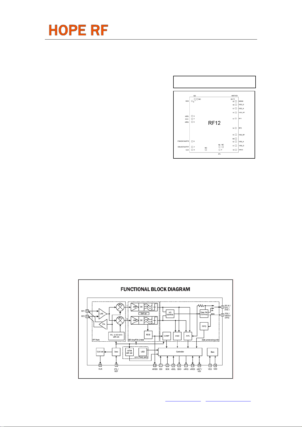
RF12
RF12 Universal ISM Band
FSK Transceiver
DESCRIPTION
Hope’s RF12 is a single chip, low power, multi-channel
FSK transceiver designed for use in applications requiring
FCC or ETSI conformance for unlicensed use in the 315, 433,
868 and 915 MHz bands. The RF12 transceiver produces a
flexible, low cost, and highly integrated solution that does not
require production alignments. The chip is a complete analog
RF and baseband transceiver including a multi-band PLL
synthesizer with PA, LNA, I/Q down converter mixers,
baseband filters and amplifiers, and an I/Q demodulator. All
required RF functions are integrated. Only an external crystal and bypass filtering are needed for
operation.
The RF12 features a completely integrated PLL for easy RF design, and its rapid settling time allows
for fast frequency-hopping, bypassing multi-path fading and interference to achieve robust wireless links.
The PLL’s high resolution allows the usage of multiple channels in any of the bands. The receiver
baseband bandwidth (BW) is programmable to accommodate various deviation, data rate and crystal
tolerance requirements. The transceiver employs the Zero-IF approach with I/Q demodulation.
Consequently, no external components (except crystal and decoupling) are needed in most applications.
The RF12 dramatically reduces the load on the microcontroller with the integrated digital data
processing features: data filtering, clock recovery, data pattern recognition, integrated FIFO and TX data
register. The automatic frequency control (AFC) feature allows the use of a low accuracy (low cost)
crystal. To minimize the system cost, the RF12 can provide a clock signal for the microcontroller, avoiding
the need for two crystals.
For low power applications, the RF12 supports low duty cycle operation based on the internal
wake-up timer.
RF12
Tel: +86-755-86096587 Fax: +86-755-86096602 E-mail: sales@hoperf.com http://www.hoperf.com
Page 2

RF12
FEATURES
Fully integrated (low BOM, easy design-in)
No alignment required in production
Fast-settling, programmable, high-resolution PLL synthesizer
Fast frequency-hopping capability
High bit rate (up to 115.2 kbps in digital mode and 256 kbps in analog mode)
Direct differential antenna input/output
Integrated power amplifier
Programmable TX frequency deviation (15 to 240 KHz)
Programmable RX baseband bandwidth (67 to 400 kHz)
Analog and digital RSSI outputs
Automatic frequency control (AFC)
Data quality detection (DQD)
Internal data filtering and clock recovery
RX synchron pattern recognition
SPI compatible serial control interface
Clock and reset signals for microcontroller
16 bit RX Data FIFO
Two 8 bit TX data registers
Low power duty cycle mode
Standard 10 MHz crystal reference
Wake-up timer
Low power consumption
Low standby current (0.3 µA)
TYPICAL APPLICATIONS
Remote control
Home security and alarm
Wireless keyboard/mouse and other PC peripherals
Toy controls
Remote keyless entry
Tire pressure monitoring
Tel e m etr y
Personal/patient data logging
Remote automatic meter reading
Tel: +86-755-86096587 Fax: +86-755-86096602 E-mail: sales@hoperf.com http://www.hoperf.com
Page 3
RF12
DETAILED FEATURE-LEVEL DESCRIPTION
The RF12 FSK transceiver is designed to cover the unlicensed frequency bands at 315, 433, 868
and 915 MHz. The devices facilitate compliance with FCC and ETSI requirements.
The receiver block employs the Zero-IF approach with I/Q demodulation, allowing the use of a
minimal number of external components in a typical application. The RF12 incorporates a fully integrated
multi-band PLL synthesizer, PA with antenna tuning, an LNA with switch-able gain, I/Q down converter
mixers, baseband filters and amplifiers, and an I/Q demodulator followed by a data filter.
PLL
The programmable PLL synthesizer determines the operating frequency, while preserving accuracy
based on the on-chip crystal-controlled reference oscillator. The PLL’s high resolution allows the usage of
multiple channels in any of the bands.
The RF VCO in the PLL performs automatic calibration, which requires only a few microseconds.
Calibration always occurs when the synthesizer starts. If temperature or supply voltage changes
significantly, VCO recalibration can be invoked easily. Recalibration can be initiated at any time by
switching the synthesizer off and back on again.
RF Power Amplifier (PA)
The power amplifier has an open-collector differential output and can directly drive a loop antenna
with a programmable output power level. An automatic antenna tuning circuit is built in to avoid costly
trimming procedures and the so-called “hand effect.”
LNA
The LNA has 250 Ohm input impedance, which functions well with the proposed antennas. If the
RF input of the chip is connected to 50 Ohm devices, an external matching circuit is required to provide
the correct matching and to minimize the noise figure of the receiver.
The LNA gain can be selected (0, –6, –14, –20 dB relative to the highest gain) according to RF signal
strength. It can be useful in an environment with strong interferers.
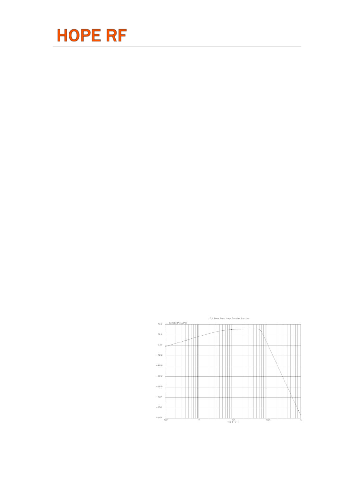
Baseband Filters
The receiver bandwidth is s
by programming the bandwidth (
the baseband filters. This allows setting
up the receiver according to the
characteristics of the signal to be
received.
An appropriate bandwidth can be
chosen to accommodate various FSK
deviation, data rate and crystal tolerance
requirements. The filter structure is 7th
order Butterworth low-pass with 40 dB
suppression at 2*BW frequency. Offset cancellation is done by using a high-pass filter with a cut-off
frequency below 7 kHz.
electable
BW) of
Tel: +86-755-86096587 Fax: +86-755-86096602 E-mail: sales@hoperf.com http://www.hoperf.com
Page 4
RF12
Data Filtering and Clock Recovery
Output data filtering can be completed by an external capacitor or by using digital filtering according
to the final application.
Analog operation: The filter is an RC type low-pass filter followed by a Schmitt-trigger (St). The
resistor (10 kOhm) and the St are integrated on the chip. An (external) capacitor can be chosen
according to the actual bit rate. In this mode, the receiver can handle up to 256 kbps data rate. The FIFO
can not be used in this mode and clock is not provided for the demodulated data.
Digital operation: A digital filter is used with a clock frequency at 29 times the bit rate. In this mode
there is a clock recovery circuit (CR), which can provide synchronized clock to the data. Using this clock
the received data can fill a FIFO. The CR has three operation modes: fast, slow, and automatic. In slow
mode, its noise immunity is very high, but it has slower settling time and requires more accurate data
timing than in fast mode. In automatic mode the CR automatically changes between fast and slow mode.
The CR starts in fast mode, then after locking it automatically switches to slow mode (Only the digital data
filter and the clock recovery use the bit rate clock. For analog operation, there is no need for setting the
correct bit rate.)
Data Validity Blocks
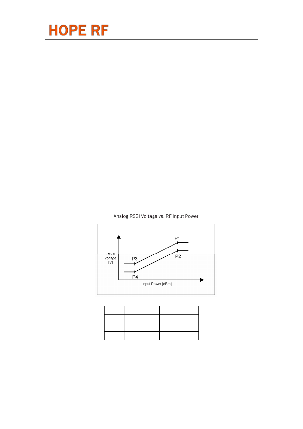
RSSI
A digital RSSI output is provided to monitor the input signal level. It goes high if the received signal
strength exceeds a given preprogrammed level. An analog RSSI signal is also available. The RSSI
settling time depends on the external filter capacitor. Pin 19 is used as analog RSSI output. The digital
RSSI can be monitored by reading the status register.
P1 -65 dBm 1300 mV
P2 -65 dBm 1000 mV
P3 -100 dBm 600 mV
P4 -100 dBm 300 mV
DQD
The Data Quality Detector is based on counting the spikes on the unfiltered received data. For
correct operation, the “DQD threshold” parameter must be filled in by using the Data Filter Command.
AFC
By using an integrated Automatic Frequency Control (AFC) feature, the receiver can minimize the
TX/RX offset in discrete steps, allowing the use of:
Tel: +86-755-86096587 Fax: +86-755-86096602 E-mail: sales@hoperf.com http://www.hoperf.com
Page 5

RF12
1, Inexpensive, low accuracy crystals
2, Narrower receiver bandwidth (i.e. increased sensitivity)
3, Higher data rate
Crystal Oscillator
The RF12 has a single-pin crystal oscillator circuit, which provides a 10 MHz reference signal for the
PLL. To reduce external parts and simplify design, the crystal load capacitor is internal and
programmable. Guidelines for selecting the appropriate crystal can be found later in this datasheet.
The transceiver can supply the clock signal for the microcontroller; so accurate timing is possible
without the need for a second crystal.
When the microcontroller turns the crystal oscillator off by clearing the appropriate bit using the
Configuration Setting Command, the chip provides a fixed number (196) of further clock pulses (“clock
tail”) for the microcontroller to let it go to idle or sleep mode.
Low Battery Voltage Detector
The low battery detector circuit monitors the supply voltage and generates an interrupt if it falls below
a programmable threshold level. The detector circuit has 50mV hysteresis.
Wake-Up Timer
The wake-up timer has very low current consumption (1.5μA typical) and can be programmed from
1 ms to several days with an accuracy of ±5%.
It calibrates itself to the crystal oscillator at every startup, and then at every 30 seconds. When the
crystal oscillator is switched off, the calibration circuit switches it back on only long enough for a quick
calibration (a few milliseconds) to facilitate accurate wake-up timing.
Event Handling
In order to minimize current consumption, the transceiver supports different power saving modes.
Active mode can be initiated by several wake-up events (negative logical pulse on nINT input, wake-up
timer timeout, low supply voltage detection, on-chip FIFO filled up or receiving a request through the
serial interface).
If any wake-up event occurs, the wake-up logic generates an interrupt signal, which can be used to
wake up the microcontroller, effectively reducing the period the microcontroller has to be active. The
source of the interrupt can be read out from the transceiver by the microcontroller through the SDO pin.
Interface and Controller
An SPI compatible serial interface lets the user select the frequency band, center frequency of the
synthesizer, and the bandwidth of the baseband signal path. Division ratio for the microcontroller clock,
wake-up timer period, and low supply voltage detector threshold are also programmable. Any of these
auxiliary functions can be disabled when not needed. All parameters are set to default after power-on; the
programmed values are retained during sleep mode. The interface supports the read-out of a status
register, providing detailed information about the status of the transceiver and the received data.
The transmitter block is equipped with an 8 bit wide TX data register. It is possible to write 8 bits into
the register in burst mode and the internal bit rate generator transmits the bits out with the predefined
rate.
It is also possible to store the received data bits into a FIFO register and read them out in a buffered
mode.
Tel: +86-755-86096587 Fax: +86-755-86096602 E-mail: sales@hoperf.com http://www.hoperf.com
Page 6
RF12
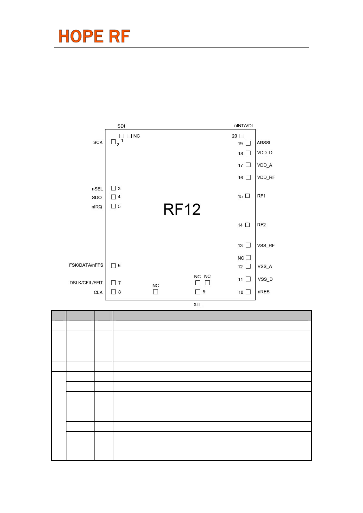
PACKAGE PIN DEFINITIONS
Pin type key: D=digital, A=analog, S=supply, I=input, O=output, IO=input/output
Pin Name Type Function
1 SDI DI Data input of the serial control interface (SPI compatible)
2 SCK DI Clock input of the serial control interface
3 nSEL DI Chip select input of the serial control interface (active low)
4 SDO DO Serial data output with bus hold
5 nIRQ DO Interrupt request output (active low)
FSK DI Transmit FSK data input
6 DATA DO Received data output (FIFO not used)
nFFS DI FIFO select input (active low) In FIFO mode, when bit ef is set in Configuration
Setting Command
DLCK DO Received data clock output (Digital filter used, FIFO not used)
CFIL AIO External data filter capacitor connection (Analog filter used) 7
FIFO interrupt (active high) Number of the bits in the RX FIFO that reach the
FFIT DO
Tel: +86-755-86096587 Fax: +86-755-86096602 E-mail: sales@hoperf.com http://www.hoperf.com
preprogrammed limit In FIFO mode, when bit ef is set in Configuration Setting
Command
Page 7
RF12
8 CLK DO Microcontroller clock output
XTL AIO
9
REF AIO External reference input. Use 33 pF series coupling capacitor
10 nRES DIO Open drain reset output with internal pull-up and input buffer (active low)
11 VSS_D S Digital VSS(Connect to VSS)
12 VSS_A S Analog VSS(Connect to VSS)
13 VSS_RF S RF VSS(Connect to VSS)
14 RF2 AIO RF differential signal input/output
15 RF1 AIO RF differential signal input/output
16 VDD_RF S RF VDD(Connect to VDD)
17 VDD_A S Analog VDD(Connect to VDD)
18 VDD_D S Digital VDD(Connect to VDD)
19 ARSSI AO Analog RSSI output
nINT DI Interrupt input (active low)
20
VDI DO Valid data indicator output
Note: The actual mode of the multipurpose pins (pin 6 and 7) is determined by the TX/RX data I/O
settings of the transceiver.
Crystal connection (the other terminal of crystal to VSS) or external reference
input
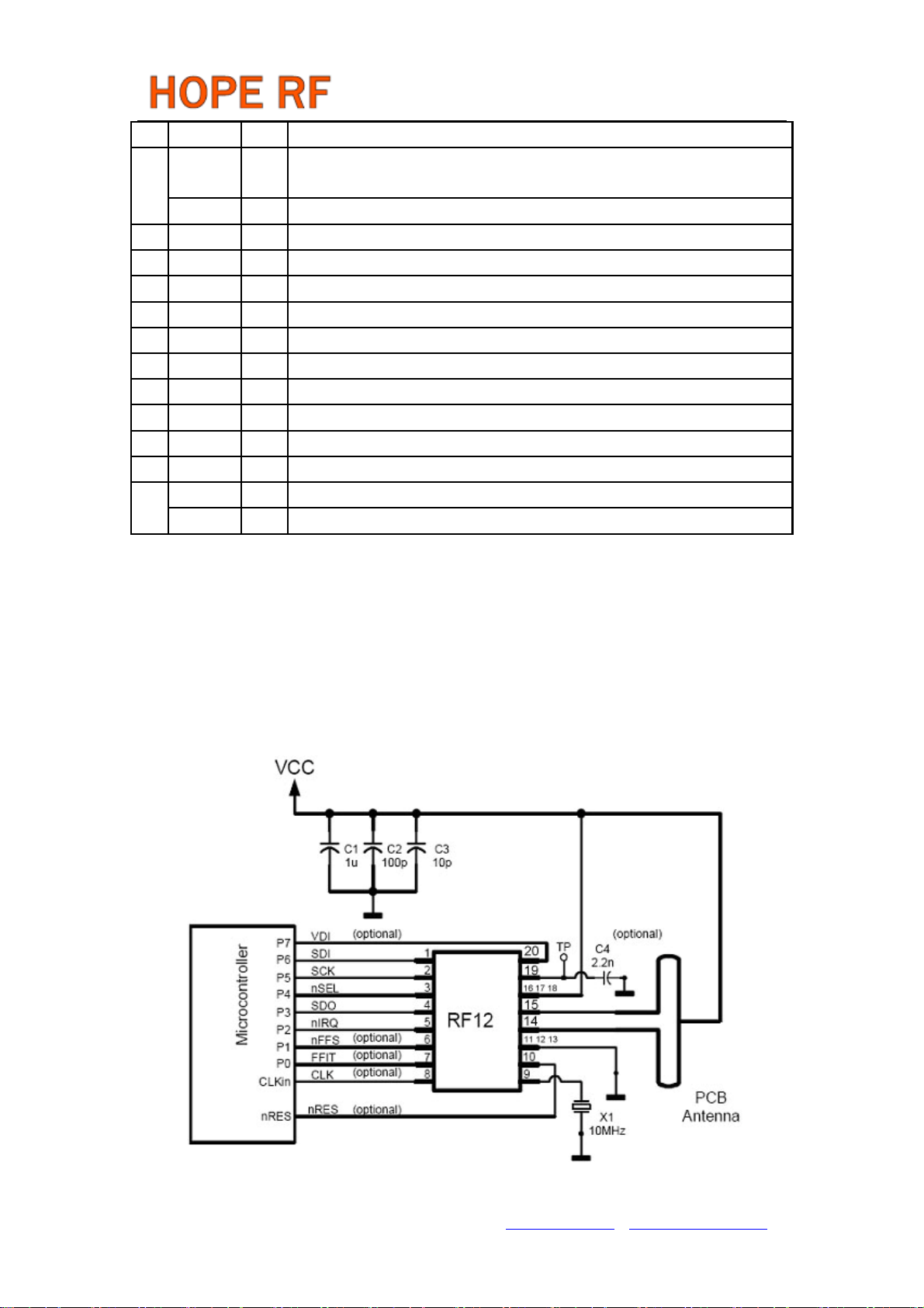
T ypical Application
Typical application with FIFO usage
Tel: +86-755-86096587 Fax: +86-755-86096602 E-mail: sales@hoperf.com http://www.hoperf.com
Page 8
RF12
Pin 6 Pin 7
Transmit mode el=0 in Configuration Setting Command TX Data input -
Transmit mode el=1 in Configuration Setting Command Connect to logic high -
Receive mode ef=0 in Configuration Setting Command RX Data output RX Data clock output
Receive mode ef=1 in Configuration Setting Command nFFS input FFIT output
GENERAL DEVICE SPECIFICATION
All voltages are referenced to Vss, the potential on the ground reference pin VSS.
Absolute Maximum Ratings (non-operating)
Symbol Parameter Min Max Units
Vdd Positive supply voltage -0.5 6 V
Vin Voltage on any pin (except RF1 and RF2) -0.5 Vdd+0.5 V
Voc Voltage on open collector outputs (RF1, RF2) -0.5 Vdd+1.5 (Note 1) V
Iin Input current into any pin except VDD and VSS -25 25 mA
ESD Electrostatic discharge with human body model 1000 V
Tst Storage temperature -55 125 oC
Recommended Operating Range
Symbol Parameter Min Max Units
Vdd Positive supply voltage 2.2 5.4 V
V
ocDC
V
ocAC
Top Ambient operating temperature -40 85
Note 1: At maximum, V
Note 2: At maximum, V
DC voltage on open collector outputs (RF1,RF2) Vdd+1.5(Note2) V
AC peak voltage on open collector outputs (RF1,RF2) Vdd-1.5(Note1) Vdd+1.5 V
℃
+1.5V cannot be higher than 7V. At minimum, Vdd-1.5V cannot be lower than 1.2V.
dd
+1.5V cannot be higher than 5.5V.
dd
ELECTRICAL SPECIFICATION
(Min/max values are valid over the whole recommended operating range. Typical conditions: Top= 27℃; Vdd=Voc=2.7V)
DC Characteristics
Symbol Parameter Conditions/Notes Min Typ Max Units
I
dd_TX_0
I
dd_TX_PMAX
Supply current (TX mode,
Pout = 0 dBm)
Supply current (TX mode,
Pout = Pmax)
315/433 MHz bands
868 MHz band
915 MHz band
315/433 MHz bands
868 MHz band
915 MHz band
13
21
16
17
23
24
14
18
19
22
25
26
mA
mA
Tel: +86-755-86096587 Fax: +86-755-86096602 E-mail: sales@hoperf.com http://www.hoperf.com
Page 9

RF12
I
dd_RX
I
pd
I
lb
I
wt
I
x
V
lb
V
lba
V
il
V
ih
I
il
I
ih
V
ol
V
oh
Supply current (RX mode)
Standby current (Sleep
mode)
Low battery voltage
detector current
315/433 MHz bands
11
868 MHz band
915 MHz band
All blocks disabled
12
13
0.3
0.5
13
14
15
mA
µA
µA
consumption
Wake-up timer current
consumption
Idle current
Low battery detect
threshold
Low battery detection
accuracy
Digital input low level
voltage
Digital input high level
voltage
Crystal oscillator and
baseband parts are on
Programmable in 0.1 V
steps
2.2
0.7*V
dd
1.5
µA
3 3.5 mA
5.3 V
±75
0.3*V
V
dd
mV
V
Digital input current Vil = 0 V -1 1 µA
Digital input current Vih = Vdd, Vdd = 5.4 V -1 1 µA
Digital output low level Iol = 2 mA 0.4 V
Digital output high level Ioh = -2 mA Vdd-0.4 V
AC Characteristics (PLL parameters)
Symbol Parameter Conditions/Notes Min Typ Max Units
ref
PLL reference
frequency
f
Receiver LO /
Transmitter carrier
f
o
frequency
t
t
st, P
PLL lock time
lock
PLL startup time With a running crystal oscillator 250 us
Tel: +86-755-86096587 Fax: +86-755-86096602 E-mail: sales@hoperf.com http://www.hoperf.com
(Note 1) 8 10 12 MHz
315MHz band,2.5kHz resolution
433MHz band,2.5kHz resolution
868MHz band,5.0kHz resolution
915MHz band,7.5kHz resolution
Frequency error < 1kHz after
10MHz step
310.24
430.24
860.48
900.72
20 us
319.75
439.75
879.51
MHz
929.27
Page 10

RF12
AC Characteristics (Receiver)
Symbol Parameter Conditions/Notes Min Typ Max Units
FSK
75
150
225
300
375
450
kHz
dBm
dBm
dBm
dBm
dBm
dBm
pF
nF
dB
us
67
60
120
180
240
300
360
134
200
270
350
400
BW
Receiver
bandwidth
mode 0
mode 1
mode 2
mode 3
mode 4
mode 5
BR FSK bit rate With internal digital filters 0.6 115.2 kbps
BRA FSK bit rate With analog filter 256 kbps
P
AFC
IIP3
IIP3
IIP3
IIP3
P
RS
RS
C
RS
min
range
inh
outh
outl
max
C
in
a
ARSSI
step
Receiver
Sensitivity
AFC locking range df
Input IP3 In band interferers in high bands(868,
Input IP3 Out of band interferers l f-fo l > 4 MHz -18
IIP3 (LNA –6 dB
inl
gain)
IIP3 (LNA –6 dB
gain)
Maximum input
power
RF input
capacitance
RSSI accuracy +/-5 dB
RSSI range 46 dB
r
Filter capacitor for
ARSSI
RSSI
programmable
BER 10-3, BW=67kHz, BR=1.2kbps
-109 -100
(Note 2)
: FSK deviation in the received
FSK
0.8*df
signal
-21
915 MHz)
In band interferers in low bands (315,
-15
433 MHz)
Out of band interferers l f-fo l > 4 MHz -12
LNA: high gain 0
1
1
6
level steps
500
RS
DRSSI response
time
resp
Until the RSSI signal goes high after
the input signal exceeds the
preprogrammed limit C
ARRSI
= 5 nF
AC Characteristics (Transmitter)
Symbol Parameter Conditions/Notes Min Typ Max Units
I
OUT
Open collector output DC
current
Available output power with
P
max
optimal antenna impedance
(Note 3, 4)
P
Typical output power
out
Psp Spurious emission
Programmable 0.5
In low bands
In high bands
Selectable in 3 dB steps
(Note 5)
At max power with loop
P
max
antenna (Note 6)
Tel: +86-755-86096587 Fax: +86-755-86096602 E-mail: sales@hoperf.com http://www.hoperf.com
8
4
-21
6 mA
dBm
P
dBm
max
-50 dBc
Page 11

RF12
Output capacitance (set by the
C
o
automatic antenna tuning
In low bands
In high bands
2
2.1
2.6
2.7
3.2
3.3
pF
circuit)
Qo
L
out
Quality factor of the output
capacitance
Output phase noise
In low bands
In high bands
100 kHz from carrier 1
MHz from carrier
13
8
-75
15
10
17
12
-85
dBc/Hz
BR FSK bit rate 256 kbps
df
FSK frequency deviation
fsk
Programmable in 15 kHz
steps
15
240 kHz
AC Characteristics (Turn-on/Turnaround timings)
Symbol Parameter Conditions/Notes Min Typ Max Units
tsx
T
tx_rx_XTAL_ON
T
rx_tx_XTAL_ON
T
tx_rx_SYNT_ON
T
rx_tx_SYNT_ON
Crystal oscillator
startup time
Transmitter -
Receiver turnover
time
Receiver
-Transmitter
turnover time
Transmitter -
Receiver turnover
time
Receiver
-Transmitter
turnover time
Crystal ESR < 100
Synthesizer off, crystal oscillator on
during TX/RX change with 10 MHz
step
Synthesizer off, crystal oscillator on
during RX/TX change with 10 MHz
step
Synthesizer and crystal oscillator on
during TX/RX change with 10 MHz
step
Synthesizer and crystal oscillator on
during RX/TX change with 10 MHz
step
450
350
425
300
5 ms
us
us
us
us
AC Characteristics (Others)
Symbol Parameter Conditions/Notes Min Typ Max Units
Cxl
t
POR
t
PBt
C
in, D
t
r , f
Crystal load capacitance, see
crystal selection guide
Internal POR timeout
Wake-up timer clock period Calibrated every 30 seconds 0.95 1.05 ms
Digital input capacitance 2 pF
Digital output rise/fall time 15 pF pure capacitive load 10 ns
Programmable in 0.5 pF steps,
tolerance +/- 10%
After V
has reached 90% of
dd
final value (Note 7)
Note 1: Not using a 10 MHz crystal is allowed but not recommended because all crystal referred timing
and frequency parameters will change accordingly.
Note 2: See the BER diagrams in the measurement results section for detailed information (Not available
at this time).
Note 3: See matching circuit parameters and antenna design guide for information.
Tel: +86-755-86096587 Fax: +86-755-86096602 E-mail: sales@hoperf.com http://www.hoperf.com
8.5
16 pF
100 ms
Page 12

RF12
Note 4: Optimal antenna admittance/impedance:
RF12 Yantenna [S] Zantenna [Ohm] Lantenna [nH]
315 MHz 1.5E-3 -j5.14E-3 52 + j179 98.00
433 MHz 1.4E-3 -j7.1E-3 27 + j136 52.00
868 MHz 2E-3 -j1.5E-2 8.7 + j66 12.50
915 MHz 2.2E-3 -j1.55E-2 9 + j63 11.20
Note 5: Adjustable in 8 steps.
Note 6: With selective resonant antennas
Note 7: During this period, commands are not accepted by the chip.
CONTROL INTERFACE
Commands to the transmitter are sent serially. Data bits on pin SDI are shifted into the device upon
the rising edge of the clock on pin SCK whenever the chip select pin nSEL is low. When the nSEL signal
is high, it initializes the serial interface. All commands consist of a command code, followed by a varying
number of parameter or data bits. All data are sent MSB first (e.g. bit 15 for a 16-bit command). Bits
having no influence (don’t care) are indicated with X. The Power On Reset (POR) circuit sets default
values in all control and command registers.
The receiver will generate an interrupt request (IT) for the microcontroller - by pulling the
nIRQ pin low - on the following events:
· The TX register is ready to receive the next byte (RGIT)
· The FIFO has received the preprogrammed amount of bits (FFIT)
· Power-on reset (POR)
· FIFO overflow (FFOV) / TX register under run (RGUR)
· Wake-up timer timeout (WKUP)
· Negative pulse on the interrupt input pin nINT (EXT)
· Supply voltage below the preprogrammed value is detected (LBD)
FFIT and FFOV are applicable when the FIFO is enabled. RGIT and RGUR are applicable only when the
TX register is enabled. To identify the source of the IT, the status bits should be read out.
Timing Specification
Symbol Parameter Minimum Value [ns]
tCH Clock high time 25
tCL Clock low time 25
tSS Select setup time (nSEL falling edge to SCK rising edge) 10
tSH Select hold time (SCK falling edge to nSEL rising edge) 10
t
Select high time 25
SHI
tDS Data setup time (SDI transition to SCK rising edge) 5
tDH Data hold time (SCK rising edge to SDI transition) 5
tOD Data delay time 10
Tel: +86-755-86096587 Fax: +86-755-86096602 E-mail: sales@hoperf.com http://www.hoperf.com
Page 13

RF12
Timing Diagram
Control Commands
Control Command Related Parameters/Functions
Configuration Setting
1
Command
Power Management
2
Command
Frequency Setting
3
Command
4 Data Rate Command Bit rate cs, r6 to r0
5 Receiver Control Command
6 Data Filter Command Data filter type, clock recovery parameters
FIFO and Reset Mode
7
Command
Receiver FIFO Read
8
Command
9 AFC Command AFC parameters
TX Configuration Control
10
Command
Transmitter Register Write
11
Command
12 Wake-Up Timer Command Wake-up time period
13 Low Duty-Cycle Command Enable low duty-cycle mode. Set duty-cycle. d6 to d0, en
Frequency band, crystal oscillator load
capacitance, baseband filter bandwidth, etc.
Receiver/Transmitter mode change,
synthesizer, xtal osc, PA, wake-up timer, clock
output can be enabled here
Data frequency of the local oscillator/carrier
signal
Function of pin 20, Valid Data Indicator,
baseband bw, LNA gain, digital RSSI threshold
Data FIFO IT level, FIFO start control, FIFO
enable and FIFO fill enable
RX FIFO can be read with this command
Modulation parameters, output power, ea
TX data register can be written with this
command
Related control
bits
el, ef, b1 to b0,
x3 to x0
er, ebb, et, es,
ex, eb, ew, dc
f11 to f0
p20, d1 to d0, i2
to i0, g1 to g0,
r2 to r0
al, ml, s1 to s0,
f2 to f0
f3 to f0, s1 to s0,
ff, fe
a1 to a0, rl1 to
rl0, st, fi, oe, en
mp, m3 to m0,
p2 to p0
t7 to t0
r4 to r0, m7 to
m0
Tel: +86-755-86096587 Fax: +86-755-86096602 E-mail: sales@hoperf.com http://www.hoperf.com
Page 14

RF12
Low Battery Detector and
Microcontroller Clock Divider
14
Command
15 Status Read Command Status bits can be read out
In general, setting the given bit to one will activate the related function. In the following tables, the POR
column shows the default values of the command registers after power-on.
LBD voltage and microcontroller clock division
ratio
d2 to d0, v4 to
v0
Description of the Control Commands
1. Configuration Setting Command
bit 15 14 13 12 11 10 9 8 7 6 5 4 3 2 1 0 POR
1 0 0 0 0 0 0 0 el ef b1 b0 x3 x2 x1 x0 8008h
Bit el enables the internal data register. If the data register is used the FSK pin must be connected to
logic high level.
Bit ef enables the FIFO mode. If ef=0 then DATA (pin 6) and DCLK (pin 7) are used for data and data
clock output.
b1 b0 Frequency Band {MHz]
0 0 315
0 1 433
1 0 868
1 1 915
2. Power Management Command
bit 15 14 13 12 11 10 9 8 7 6 5 4 3 2 1 0 POR
1 0 0 0 0 0 1 0 er ebb et es ex eb ew dc 8208h
Bit Function of the control bit Related blocks
Enables the whole receiver chain RF front end, baseband,
er
ebb The receiver baseband circuit can be separately switched on Baseband
Switches on the PLL, the power amplifier, and starts the
et
transmission (If TX register is enabled)
es Turns on the synthesizer Synthesizer
ex Turns on the crystal oscillator Crystal oscillator
eb Enables the low battery detector Low battery detector
ew Enables the wake-up timer Wake-up timer
dc Disables the clock output (pin 8) Clock output buffer
The ebb, es, and ex bits are provided to optimize the TX to RX or RX to TX turnaround time.
x3 x2 x1 x0 Crystal Load Capacitance [pF]
0 0 0 0 8.5
0 0 0 1 9.0
0 0 1 0 9.5
0 0 1 1 10.0
1 1 1 0 15.5
1 1 1 1 16.0
…
synthesizer, oscillator
Power amplifier, synthesizer,
oscillator
Tel: +86-755-86096587 Fax: +86-755-86096602 E-mail: sales@hoperf.com http://www.hoperf.com
Page 15

RF12
Logic connections between power control bits:
3. Frequency Setting Command
bit 15 14 13 12 11 10 9 8 7 6 5 4 3 2 1 0 POR
1 0 1 0 f11 f10f9f8f7f6f5f4f3f2f1 f0 A680h
The 12-bit parameter F (bits f11 to f0) should be in the range of 96 and 3903. When F value sent is out of
range, the previous value is kept. The synthesizer band center frequency f
f
= 10 * C1 * (C2 + F/4000) [MHz]
0
The constants C1 and C2 are determined by the selected band as:
Band [MHz] C1 C2
315 1 31
433 1 43
868 2 43
915 3 30
Tel: +86-755-86096587 Fax: +86-755-86096602 E-mail: sales@hoperf.com http://www.hoperf.com
can be calculated as:
0
Page 16

RF12
4. Data Rate Command
bit 15 14 13 12 11 10 9 8 7 6 5 4 3 2 1 0 POR
1 1 0 0 0 1 1 0 cs r6 r5 r4 r3 r2 r1 r0 C623h
The actual bit rate in transmit mode and the expected bit rate of the received data stream in receive
mode is determined by the 7-bit parameter R (bits r6 to r0) and bit cs.
BR = 10000 / 29 / (R+1) / (1+cs*7) [kbps]
In the receiver set R according to the next function:
R= (10000 / 29 / (1+cs*7) / BR) – 1, where BR is the expected bit rate in kbps.
Apart from setting custom values, the standard bit rates from 600 bps to 115.2 kbps can be
approximated with small error. Data rate accuracy requirements:
Clock recovery in slow mode: ∆BR/BR < 1/(29*N
Clock recovery in fast mode: ∆BR/BR < 3/(29*N
BR is the bit rate set in the receiver and ∆BR is the bit rate difference between the transmitter and
the receiver. N
is the maximal number of consecutive ones or zeros in the data stream. It is
bit
recommended for long data packets to include enough 1/0 and 0/1 transitions, and be careful to use the
same division ratio in the receiver and in the transmitter.
5. Receiver Control Command
bit 15 14 13 12 11 10 9 8 7 6 5 4 3 2 1 0 POR
1 0 0 1 0 p20 d1 d0 i2 i1 i0 g1 g0 r2 r1 r0 9080h
Bit 10 (p20): pin20 function select
p20 Function of pin 20
0 Interrupt input
1 VDI output
Bits 9-8 (d1 to d0): VDI (valid data indicator) signal response time setting:
d1 d0 Response
0 0 Fast
0 1 Medium
1 0 Slow
1 1 Always on
)
bit
)
bit
Tel: +86-755-86096587 Fax: +86-755-86096602 E-mail: sales@hoperf.com http://www.hoperf.com
Page 17

RF12
Bits 7-5 (i2 to i0): Receiver baseband bandwidth (BW) select:
i2 i1 i0 BW [kHz]
0 0
0 reserved
0 0 1 400
0 1
0 1
1 0
1 0
1 1
1 1
0 340
1 270
0 200
1 134
0 67
1 reserved
Bits 4-3 (g1 to g0): LNA gain select:
Bits 2-0 (r2 to r0): RSSI detector threshold:
r2 r1 r0
RSSIsetth [dBm]
0 0 0 -103
0 0 1 -97
0 1 0 -91
0 1 1 -85
1 0 0 -79
1 0 1 -73
1 1 0 -67
1 0 1 -61
g1 g0 relative to maximum [dB]
0 0 0
0 1 -6
1 0 -14
1 1 -20
The RSSI threshold depends on the LNA gain, the real RSSI threshold can be calculated:
RSSI
= RSSI
th
setth
+ G
LNA
6. Data Filter Command
bit 15 14 13 12 11 10 9 8 7 6 5 4 3 2 1 0 POR
1 1 0 0 0 0 1 0 al ml 1 s 1 f2 f1 f0 C22Ch
Bit 7 (al) : Clock recovery (CR) auto lock control, if set.
CR will start in fast mode, then after locking it will automatically switch to slow mode.
Bit 6 (ml): Clock recovery lock control
1: fast mode, fast attack and fast release (6 to 8 bit preamble (1010...) is recommended)
0: slow mode, slow attack and slow release (12 to 16 bit preamble is recommended)
Using the slow mode requires more accurate bit timing (see Data Rate Command).
Bits 4 (s): Select the type of the data filter:
s Filter Type
0 Digital filter
1 Analog RC filter
Digital: This is a digital realization of an analog RC filter followed by a comparator with
hysteresis. The time constant is automatically adjusted to the bit rate defined by the Data Rate
Command.
Note: Bit rate can not exceed 115 kpbs in this mode. Analog RC filter: The demodulator
output is fed to pin 7 over a 10 kOhm resistor. The filter cut-off frequency is set by the external
capacitor connected to this pin and VSS. C = 1 / (3 * R * Bit Rate), therefore the suggested
value for 9600 bps is 3.3 nF
Note: If analog RC filter is selected the internal clock recovery circuit and the FIFO can not
be used.
Tel: +86-755-86096587 Fax: +86-755-86096602 E-mail: sales@hoperf.com http://www.hoperf.com
Page 18

RF12
Bits 2-0 (f2 to f0): DQD threshold parameter.
Note: To let the DQD report "good signal quality" the threshold parameter should be less
than 4 in the case when the bit-rate is close to the deviation. At higher deviation/bit-rate
settings higher threshold parameter can report "good signal quality" as well.
7. FIFO and Reset Mode Command
bit 15 14 13 12 11 10 9 8 7 6 5 4 3 2 1 0 POR
1 1 0 0 1 0 1 0 f3 f2 f1 f0 0 al ff dr CA80h
Bits 7-4 (f4 to f0): FIFO IT level. The FIFO generates IT when the number of received data bits reaches
this level.
Bit 2 (al): Set the input of the FIFO fill start condition:
al
0 Synchron pattern
1 Always fill
Note: Synchron pattern is 2DD4h.
Note: For details see the Configuration Setting Command
For details see the Power Management Command
Bit 1 (ff): FIFO fill will be enabled after synchron pattern reception. The FIFO fill stops when this bit is
cleared.
Bit 0 (dr): Disables the highly sensitive RESET mode. If this bit is cleared, a 200 mV glitch in the power
supply may cause a system reset.
Note: To restart the synchron pattern recognition, bit 1 should be cleared and set.
8. Receiver FIFO Read Command
bit 15 14 13 12 11 10 9 8 7 6 5 4 3 2 1 0 POR
1 0 1 1 0 0 0 0 0 0 0 0 0 0 0 0 B000h
With this command, the controller can read 8 bits from the receiver FIFO. Bit 6 (ef) must be set in
Configuration Setting Command.
Tel: +86-755-86096587 Fax: +86-755-86096602 E-mail: sales@hoperf.com http://www.hoperf.com
Page 19

RF12
Note: The transceiver is in receive (RX) mode when bit er is set using the Power Management
Command
9. AFC Command
bit 15 14 13 12 11 10 9 8 7 6 5 4 3 2 1 0 POR
1 1 0 0 0 1 0 0 a1 a0 rl1 rl0 st fi oe en C4F7h
Bit 7-6 (a1 to a0): Automatic operation mode selector:
a1 a0
0 0 Auto mode off (Strobe is controlled by microcontroller)
0 1 Runs only once after each power-up
1 0 Keep the foffset only during receiving (VDI=high)
1 1 Keep the foffset value independently from the state of the VDI signal
Bit 5-4 (rl1 to rl0): Range limit. Limits the value of the frequency offset register to the next values:
rl1 rl0 Max deviation
0 0 No restriction
0 1 +15 f
1 0 +7 f
1 1 +3 f
res
to -8 f
res
to -4 f
res
to -16 f
res
res
res
f :
res
315, 433 MHz bands: 2.5 kHz
868 MHz band: 5 kHz
915 MHz band: 7.5 kHz
Bit 3 (st): Strobe edge, when st goes to high, the actual latest calculated frequency error is stored into the
offset register of the AFC block.
Bit 2 (fi): Switches the circuit to high accuracy (fine) mode. In this case, the processing time is about twice
longer, but the measurement uncertainty is about the half.
Bit 1 (oe): Enables the frequency offset register. It allows the addition of the offset register to the
frequency control word of the PLL.
Bit 0 (en): Enables the calculation of the offset frequency by the AFC circuit.
Tel: +86-755-86096587 Fax: +86-755-86096602 E-mail: sales@hoperf.com http://www.hoperf.com
Page 20

RF12
Note:
Lock bit is high when the AFC loop is locked, f same bit indicates when two subsequent measuring
results are the same, toggle bit changes state in every measurement cycle.
In automatic operation mode (no strobe signal is needed from the microcontroller to update the
output offset register) the AFC circuit is automatically enabled when the VDI indicates potential incoming
signal during the whole measurement cycle and the circuit measures the same result in two subsequent
cycles.
There are three operation modes, example from the possible application:
1, (a1=0, a0=1) The circuit measures the frequency offset only once after power up. In this way
extended TX-RX maximum distance can be achieved.
Possible application:
In the final application, when the user inserts the battery, the circuit measures and compensates for
the frequency offset caused by the crystal tolerances. This method allows for the use of a cheaper quartz
in the application and provides protection against tracking an interferer.
2a, (a1=1, a0=0) The circuit automatically measures the frequency offset during an initial effective
low data rate pattern –easier to receive (i.e.: 00110011) of the package and changes the receiving
frequency accordingly. The further part of the package can be received by the corrected frequency
settings.
2b, (a1=1, a0=0) The transmitter must transmit the first part of the packet with a step higher
deviation and later there is a possibility to reduce it.
In both cases (2a and 2b), when the VDI indicates poor receiving conditions (VDI goes low), the
output register is automatically cleared. Use these settings when receiving signals from different
transmitters transmitting in the same nominal frequencies.
3, (a1=1, a0=1) It’s the same as 2a and 2b modes, but suggested to use when a receiver operates
with only one transmitter. After a complete measuring cycle, the measured value is kept independently of
the state of the VDI signal.
Tel: +86-755-86096587 Fax: +86-755-86096602 E-mail: sales@hoperf.com http://www.hoperf.com
Page 21

RF12
10. TX Configuration Control Command
bit 15 14 13 12 11 10 9 8 7 6 5 4 3 2 1 0 POR
1 0 0 1 1 0 0 mp m3 m2 m1 m0 0 p2 p1 p0 9800h
Bits 8-4 (mp, m3 to m0):
FSK modulation parameters:
The resulting output frequency can be calculated as:
f
= f0 + (-1)
out
SIGN
* (M + 1) * (15 kHz)
where:
f
is the channel center frequency (see the Frequency Setting Command)
0
M is the four bit binary number <m3: m0>
SIGN = (mp) XOR (FSK input)
Bits 2-0 (p2 to p0): Output power:
p2 p1 p0 Relative Output Power [dB]
0 0 0 0
0 0 1 -3
0 1 0 -6
0 1 1 -9
1 0 0 -12
1 0 1 -15
1 1 0 -18
1 1 1 -21
The output power given in the table is relative to the maximum available power, which depends on the
actual antenna impedance.
11. Transmitter Register Write Command
bit 15 14 13 12 11 10 9 8 7 6 5 4 3 2 1 0 POR
1 0 1 1 1 0 0 0 t7 t6 t5 t4 t3 t2 t1 t0 B8AAh
With this command, the controller can write 8 bits (t7 to t0) to the transmitter data register. Bit 7 (el) must
be set in Configuration Setting Command.
Tel: +86-755-86096587 Fax: +86-755-86096602 E-mail: sales@hoperf.com http://www.hoperf.com
Page 22

RF12
12. Wake-Up Timer Command
bit 15 14 13 12 11 10 9 8 7 6 5 4 3 2 1 0 POR
1 1 1 r4 r3 r2 r1 r0 m7 m6 m5 m4 m3 m2 m1 m0 E196h
The wake-up time period can be calculated by (m7 to m0) and (r4 to r0):
T
= M * 2R [ms]
wake-up
Note:
• For continual operation the et bit should be cleared and set at the end of every cycle.
• For future compatibility, use R in a range of 0 and 29.
13. Low Duty-Cycle Command
bit 15 14 13 12 11 10 9 8 7 6 5 4 3 2 1 0 POR
1 1 0 0 1 0 0 r0 d6 d5 d4 d3 d2 d1 d0 en C80Eh
With this command, Low Duty-Cycle operation can be set in order to decrease the average power
consumption in receiver mode. The time cycle is determined by the Wake-Up Timer Command. The
Duty-Cycle can be calculated by using (d6 to d0) and M. (M is parameter in a Wake-Up Timer
Command.)
Duty-Cycle= (D * 2 +1) / M *100%
Bit 0 (en): Enables the Low Duty-Cycle Mode. Wake-up timer interrupt not generated in this mode.
Note: In this operation mode, bit er must be cleared and bit ew must be set in the Power Management
Command.
14. Low Battery Detector and Microcontroller Clock Divider Command
bit 15 14 13 12 11 10 9 8 7 6 5 4 3 2 1 0 POR
1 1 0 0 0 0 0 0 d2 d1 d0 v4 v3 v2 v1 v0 C000h
The 5 bit parameter (v4 to v0) represents the value V, which defines the threshold voltage Vlb of the
detector:
V
= 2.2 + V * 0.1 [V]
lb
Clock divider configuration:
d2 d1 d0 Clock Output Frequency [ M Hz]
0 0 0 1
0 0 1 1.25
0 1 0 1.66
0 1 1 2
Tel: +86-755-86096587 Fax: +86-755-86096602 E-mail: sales@hoperf.com http://www.hoperf.com
Page 23
RF12
1 0 0 2.5
1 0 1 3.33
1 1 0 5
1 1 1 10
The low battery detector and the clock output can be enabled or disabled by bits eb and dc, respectively,
using the Power Management Command.
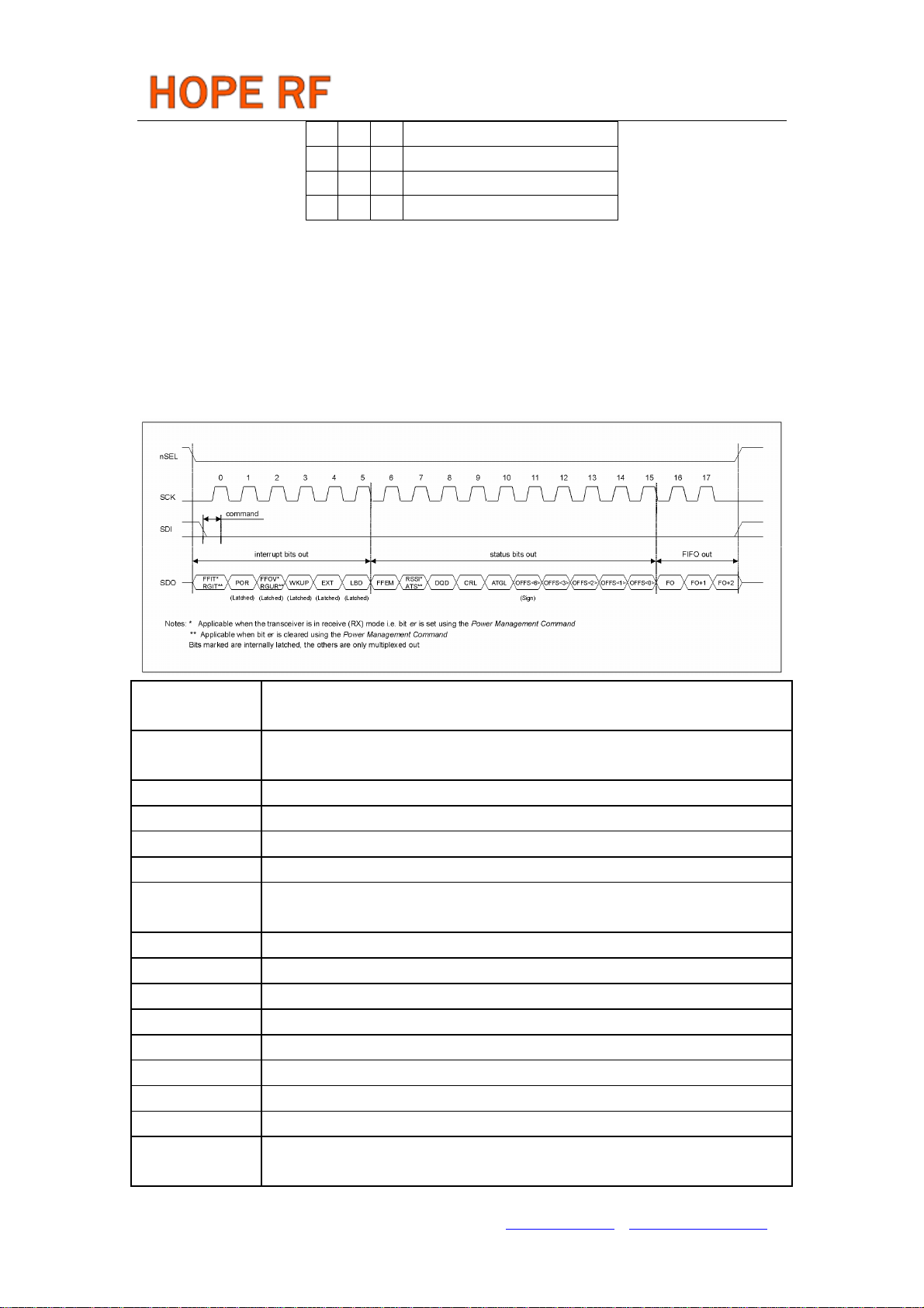
15. Status Read Command
The read command starts with a zero, whereas all other control commands start with a one. If a read
command is identified, the status bits will be clocked out on the SDO pin as follows:
Status Register Read Sequence with FIFO Read Example:
RGIT
FFIT
POR Power-on reset (Cleared after Status Read Command )
RGUR TX register under run, register over write (Cleared after Status Read Command )
FFOV RX FIFO overflow (Cleared after Status Read Command )
WKUP Wake-up timer overflow (Cleared after Status Read Command )
EXT
LBD Low battery detect, the power supply voltage is below the pre-programmed limit
FFEM FIFO is empty
ATS Antenna tuning circuit detected strong enough RF signal
RSSI The strength of the incoming signal is above the pre-programmed limit
DQD Data quality detector output
CRL Clock recovery locked
ATGL Toggling in each AFC cycle
OFFS(6) MSB of the measured frequency offset (sign of the offset value)
OFFS(3)-OFFS(0)
TX register is ready to receive the next byte (Can be cleared by Transmitter
Register Write Command )
The number of data bits in the RX FIFO has reached the pre-programmed limit (Can
be cleared by any of the FIFO read methods)
Logic level on interrupt pin (pin 16) changed to low (Cleared after Status Read
Command )
Offset value to be added to the value of the frequency control parameter (Four LSB
bits)
Tel: +86-755-86096587 Fax: +86-755-86096602 E-mail: sales@hoperf.com http://www.hoperf.com
Page 24

RF12
TX REGISTER BUFFERED DATA TRANSMISSION
In this operating mode (enabled by bit el, the Configuration Control Command) the TX data is clocked
into one of the two 8-bit data registers. The transmitter starts to send out the data from the first register
(with the given bit rate) when bit et is set with the Power Management Command. The initial value of the
data registers (AAh) can be used to generate preamble. During this mode, the SDO pin can be monitored
to check whether the register is ready (SDO is high) to receive the next byte from the microcontroller.
TX register simplified block diagram (before transmit)
TX register simplified block diagram (during transmit)
Typical TX register usage
Note: The content of the data registers are initialized by clearing bit et.
Tel: +86-755-86096587 Fax: +86-755-86096602 E-mail: sales@hoperf.com http://www.hoperf.com
Page 25

RF12
RX FIFO BUFFERED DATA READ
In this operating mode, incoming data are clocked into a 16 bit FIFO buffer. The receiver starts to fill
up the FIFO when the Valid Data Indicator (VDI) bit and the synchron pattern recognition circuit indicates
potentially real incoming data. This prevents the FIFO from being filled with noise and overloading the
external microcontroller.
Polling Mode:
The nFFS signal selects the buffer directly and its content can be clocked out through pin SDO by
SCK. Set the FIFO IT level to 1. In this case, as long as FFIT indicates received bits in the FIFO, the
controller may continue to take the bits away. When FFIT goes low, no more bits need to be taken. An
SPI read command is also available.
Interrupt Controlled Mode:
The user can define the FIFO level (the number of received bits) which will generate the nFFIT when
exceeded. The status bits report the changed FIFO status in this case.
FIFO Read Example with FFIT Polling
During FIFO access f
cannot be higher than f
SCK
/4, where f
ref
is the crystal oscillator frequency.
ref
CRYSTAL SELECTION GUIDELINES
The crystal oscillator of the RF12 requires a 10 MHz parallel mode crystal. The circuit contains an
integrated load capacitor in order to minimize the external component count. The internal load
capacitance value is programmable from 8.5 pF to 16 pF in 0.5 pF steps. With appropriate PCB layout,
the total load capacitance value can be 10 pF to 20 pF so a variety of crystal types can be used.
When the total load capacitance is not more than 20 pF and a worst case 7 pF shunt capacitance (C
value is expected for the crystal, the oscillator is able to start up with any crystal having less than 300
ohms ESR (equivalent series loss resistance). However, lower C
oscillator startup.
The crystal frequency is used as the reference of the PLL, which generates the local oscillator
frequency (f
). Therefore fLO is directly proportional to the crystal frequency. The accuracy requirements
LO
for production tolerance, temperature drift and aging can thus be determined from the maximum
Tel: +86-755-86096587 Fax: +86-755-86096602 E-mail: sales@hoperf.com http://www.hoperf.com
and ESR values guarantee faster
0
)
0
Page 26

RF12
allowable local oscillator frequency error.
Whenever a low frequency error is essential for the application, it is possible to “pull” the crystal to
the accurate frequency by changing the load capacitor value. The widest pulling range can be achieved if
the nominal required load capacitance of the crystal is in the “midrange”, for example 16 pF. The
“pull-ability” of the crystal is defined by its motional capacitance and C
.
0
RX-TX ALIGNMENT PROCEDURES
RX-TX frequency offset can be caused only by the differences in the actual reference frequency. To
minimize these errors it is suggested to use the same crystal type and the same PCB layout for the
crystal placement on the RX and TX PCBs.
To verify the possible RX-TX offset it is suggested to measure the CLK output of both chips with a
high level of accuracy. Do not measure the output at the XTL pin since the measurement process itself
will change the reference frequency. Since the carrier frequencies are derived from the reference
frequency, having identical reference frequencies and nominal frequency settings at the TX and RX side
there should be no offset if the CLK signals have identical frequencies.
It is possible to monitor the actual RX-TX offset using the AFC status report included in the status
byte of the receiver. By reading out the status byte from the receiver the actual measured offset
frequency will be reported. In order to get accurate values the AFC has to be disabled during the read by
clearing the "en" bit in the AFC Control Command (bit 0).
Tel: +86-755-86096587 Fax: +86-755-86096602 E-mail: sales@hoperf.com http://www.hoperf.com
Page 27

RF12
REFERENCE DESIGNS
Schematic
PCB layout
Top view
Bottom view
Tel: +86-755-86096587 Fax: +86-755-86096602 E-mail: sales@hoperf.com http://www.hoperf.com
Page 28

SGS Reports
RF12
Tel: +86-755-86096587 Fax: +86-755-86096602 E-mail: sales@hoperf.com http://www.hoperf.com
Page 29

RF12
Tel: +86-755-86096587 Fax: +86-755-86096602 E-mail: sales@hoperf.com http://www.hoperf.com
Page 30

RF12
RF12 BONDING DIAGRAM
Pad Opening: 85um square, except 76um octagon pads (AN1, AN2)
Die Size: 2910 X 3315 um
Tel: +86-755-86096587 Fax: +86-755-86096602 E-mail: sales@hoperf.com http://www.hoperf.com
Page 31

RF12
HOPE MICROELECTRONICS CO.,LTD
4/F, Block B3, East Industrial Area,
Huaqiaocheng, Shenzhen, Guangdong,
China
Tel: 86-755-86096602
Fax: 86-755-86096587
Email:
Website:
http://www.hoperf.cn
http://hoperf.en.alibaba.com
sales@hoperf.com
http://www.hoperf.com
This document may contain preliminary information and is subject to
change by Hope Microelectronics without notice. Hope Microelectronics
assumes no responsibility or liability for any use of the information
contained herein. Nothing in this document shall operate as an express
or implied license or indemnity under the intellectual property rights of
Hope Microelectronics or third parties. The products described in this
document are not intended for use in implantation or other direct life
support applications where malfunction may result in the direct physical
harm or injury to persons. NO WARRANTIES OF ANY KIND,
INCLUDING, BUT NOT LIMITED TO, THE IMPLIED WARRANTIES OF
MECHANTABILITY OR FITNESS FOR A ARTICULAR PURPOSE, ARE
OFFERED IN THIS DOCUMENT.
©2006, HOPE MICROELECTRONICS CO.,LTD. All rights reserved.
Tel: +86-755-86096587 Fax: +86-755-86096602 E-mail: sales@hoperf.com http://www.hoperf.com
 Loading...