

!ladleIhaeK
•
ervlce
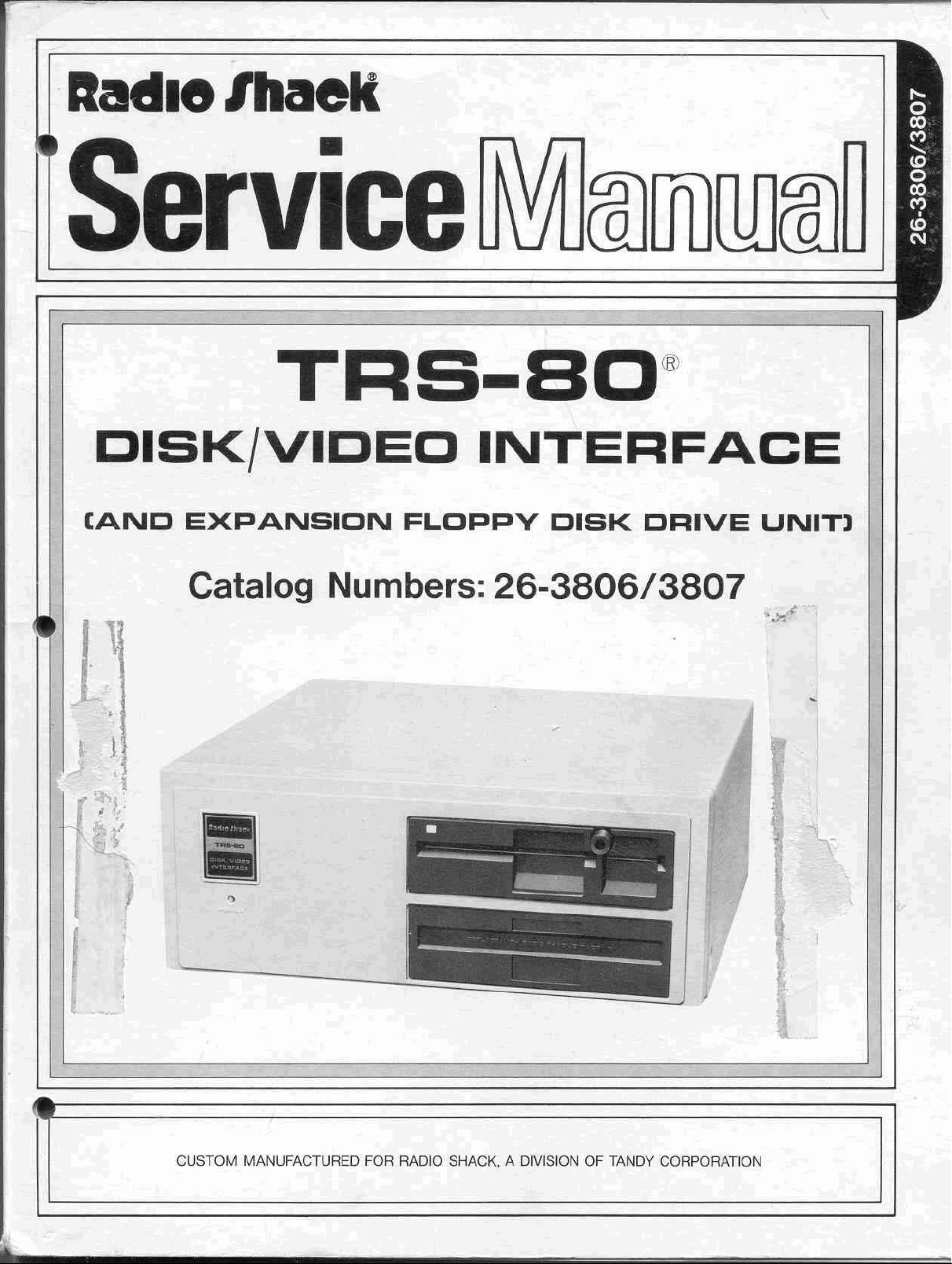
TRS-BO®
DISK/VIDEO
[AND
EXPANSION
Catalog Numbers:
l'
•
1
,
INTERFACE
FLOPPY
DISK
26-3806/3807
DRIVE
UNIT)
..
.;-:
'"
CUSTOM MANUFACTURED FOR RADIO SHACK. A DIVISION OF TANDY CORPORATION
Contents
"ill
1IINTRODUCTION
GENERAL.
SYSTEM OVERVIEW . . • . . . . . . . . . . . . . . . . . . . . . • • . . . . . . . . • • • . . . . . . . . • . . .
SPECIFICATIONS . . . . . . . . . . . . . . . . . . . . . . . . • • . . . . . . . . . . • . . . . . . . . . . . . . . 1-4
. . . . . . . . • . . . . . . . . . . . . . . . . . . . . . . . . . . . . . . . . . . . . . . . . . . • • . . 1-1
2/DISASSEMBLY INSTRUCTIONS. . . . . . . . . . . . . . . . . . . . . .. . . . . . . . . . .
TOP CASE
MAIN P.C. BOARD
POWER SUPPLY P.C. BOARD
DISK DRIVE UNIT
FRONT PANEL ASSEMBLY
.................................•••........••.........
...........................•.........•.•...........
......•..................•.•.........•......
..................•••.........••.................•.
...........•..................................
3/PREVENTIVE MAINTENANCE . . . . . .. . . . . . . . . . . . .. . . . . . . . . . . . . . .
ADJUSTMENT
SYSTEM CLOCK
POWER SUPPLY
....•..............................•.•.......•.......
........••......................................
4/THEORY OF OPERATION. . . . . . . . . . . . . . . . . . . . . . . . . . . . . . . . . . . . . .
CPU
...........................•.........••........•.........•..
ADDRESS DECODING AND BANK SELECTION CIRCUIT
MEMORY MAP
I/O
MAP
CLOCK GENERATOR CIRCUIT 4-5
SYSTEM BUS INTERFACE CIRCUIT
CRT INTERFACE AND CONTROL CIRCUIT
FLICKER SUPPRESSING CIRCUIT . . . . . . . . . . . . . . . . . • • • . . . . . . . . . . . . . . . . . • • . 4-11
FDD
INTERFACE SIGNALS
FDD
CONTROL CIRCUIT. . . . . . . . . . • . . . . . . . . . . . . . . . . . . . . . . . . . . . . . . . . . . .
POWER
SUPPLY
....•...............................•................
.....•.........•..........••.........•........••.........
...........•••........••.........•......
........•............•..................••..
AND RESET CIRCUIT
............................••.......
..
..
..
1-1
1-2
2-1
2-1
2-1
2-1
2-2
2-2
3-1
3-1
3-1
3-2
4-1
4-2
4-3
4-3
4-4
4-6
4-8
4-11
4-13
4-16
5/TROUBLESHOOTING .. . . . . . . . . . . . . . . . . . . . . . .. . . . . . . . . . . . . . . . . .
TROUBLESHOOTING FLOWCHART
CHECKING PROCEDURE
....................•..........•........•......
6/EXPLODED VIEW AND PARTS
EXPLODED VIEW
ELECTRICAL PARTS LIST
MECHANICAL/ASSEMBLY PARTS. . . . . . . . . . . . . . . . • • . . . . . . . . . . . . . . . . . . . . . .
7/P.C.
APPENDIX
BOARD
MAIN P.C. BOARD ,
MAIN P.C. BOARD -- REVISED
POWER SUPPLY P.C. BOARD
SCHEMATIC DIAGRAM
AI
•..................................................
VIEWS AND SCHEMATIC DIAGRAM 7-1
....................••.........•..........•.....
INSTALLATION OF ADDITIONAL DISK DRIVE
.....•..................................
LIST.
......•......
.••..........•........••...................
...............................••...........
UNIT.
APPENDIX B/CONNECTOR PIN ASSIGNMENTS. . . . . . . . . . . . . . . . . . . .
SYSTEM BUS CONNECTOR
RF
MODULATOR
..............................••...................•
..
..
5-1
5-1
5-2
6-1
6-1
6-2
6-13
7-1
7-3
7-5
7-6
A-1
B-1
B-1
B-2
APPENDIX C/SERVICING THE FDD UNIT" """""" """"" """" """"" """" """
PART1"MECHANICAL
1-1 INSTALLATION/REMOVALOFCOMPONENTS" " " " " " _ " " " " " " " " " " " " " " " " " " " "
1-2 ADJUSTMENT" " " " " " " " " " " " " " " " " " " " " " " " " " " " " " " " " " " " " " " " " " " " " " " C-7
1-3 SPECIAL MAINTENANCE TOOLS" " " " " " " "__" " " _" " " " " " " " " " " " " " " " " " " "
1-4 MAINTENANCE" " " " " " " " " " " " " " " " " " " " " " " " " " " " " " " " " " " " " " " " " " " " "
PART2"ELECTRICAL SECTION" " " " " " " " " " " " " " " " _ " " " " " " " " " " " " " " " " " " " " " " " "
2-1
GENERAL DESCRIPTION" " " " " " "
2-2 BLOCK
2-3
ELECTRICAL DIAGRAM" "__" " " " " " " " " " " " " " " " " " " "__" " " " " " " " " " _ " " _
2-4
INDEPENDENT LSI CONRGURATION " " " " " " " " " " " " _ " " _• " " " " " " " _ " " " " . " C-19
2-5 INPUT SIGNAL LINES (CPU TO FDD) "
2-6 OUTPUT SIGNAL LINES
PART3"CIRCUIT DlAGRAM_ " " " " " " . " " " " " " " " " " "..".." " " " " " " " " " " " " " "
PART4"TROUBLESHOOTING" " " " " " " " " ".•__
4-1 PROCESSING SOFT
4-2
FLOPPY DISK
4-3
TROUBLESHOOTING
PART5"EXPLODED VIEW AND PARTS LIST. " . " " " . " " " . " ".." " " " " " "
PART 6. SPECIAL MAINTENANCE TOOLS " " " " " " " " " " . " " " " " " " " " " " " " . " " " " " " " " . C-57
SECTION"
DIAGRAM"
DRIVE
" " " " " " " " " " " " " " " " " " " " " " " " " " " " " " " " " " " " " " " "
"""""
" " " " " " " "__" " " " " " " " " " " " " " " " " "__" " " " " " " " " " " " C-17
(FDD
TO CPU)
ERRORS"
FOR
PROCEDURES"
" " ".." " " _" " " " " " " " " " _" " " " "..".." " " " "
REPAIR" " " " " . " " " " " " " "__" _" " " " " " " " " " " " " " "
""""""
.....
"""""""""""""""""""""""
" " "__" " " " " " " " " " " • " " • ".." " " " "
" " " " " ".." _" _"__" " " " " ".." " " " "••" C-37
__
" " " " " " "
" " " " " " " " " " ".." " . " " " _" " _" "
""""""
...
" " " " " " C-17
•."...
" " " " " " " " C-47
C-1
C-1
C-1
C-15
C-15
C-1"7
C-1
C-23
C-29
C-33
C-35
C-35
C-36
B
Note: The expansion drive unit (Radio Shack Catalog Number 26-3807)isexactly
of
the
DiskNideo
Interface. When servicing
the
26-3807, refertothe
drive unit
the
sameas
portionofthis service manual.
the
built-in drive unit
j,
List
of
Illustrations
•
FIGURE
NUMBER
H
1-2
2-1
2-2
2-3
3-1
3-2
4-1
4-2
4-3
4-4
4-5
4-6
4-7
4-8
4-9
4-10
4-11
4-12
4-13
4-14
4-15
4-16
6-1
7-1
7-2
7-3
7-4
7-5
7-6
7-7
A-l
A-2
A-3
8-1
8-2
C-l
C-2
C-3
C-4
C-5
C-6
C-7
C-8
C-9
DESCRIPTiON
Disk/Video
Disk/Video
Top
Case
Removal
Disk Drive Removal .
System
+5V
Block Diagram .
CPU
Address Decoding and
Memory
Clock Generator
System
System BUS Interface Block Diagram
CRT
Display
Display
Waveform
Flicker
FDD
Data
Pre-Compensation
Wait
Exploded
Main
Main
Main P.C. Board-Revised
Main P.C. Board-Revised
Power
Power
Schematic Diagram
PreparationonP.C.B.ofFDD
InstallationofFDD
Cable
System BUS Connector .
Modulator
RF
P.C. Board Removal .
Clamp
Carrier
Pulse
Spindle
Track
Index Sensor
Winding
Mounting
Interface
Interface (Rear
Removal .
of
P.C. Board <
Clock
Adjustment
Adjustment.
Control
Interface
Interface
Separator.
Control
P.C.
P.C.
Diagram . . . . . . . . . . . . . . . . . . . . . . . . . . . . .
Map.
BUS
Interface
Timing
Timing
of
Video
Suppression
Circuit
View
Board
Board
Supply
Supply
Connections .
BaseBKand Clamp
BK
Removal
Motor
BK Removal
Motor
Sensor Removal .
Adjustment
the
Steel
the
(Front
View}
View)
. . . . . . . . . . . . . . . . . .
••••••••••••••••••••••••••••••••••••••••••••••••••
. .
..
. < • •
BANK
Selector
. . . . . . . . . . . . . . . . . . . . . . . . . . . . . . . . . . . . . . . . .
Circuit.
Block
Chart
Chart (80 Characters Mode) . . . . . . . . . .
Block
. . . . . . . . . . . . . . . . . . . . . .
(Top
(Bottom
P.C. Board
P.C. Board
. . . . . . . . .
. . . . . . . . . . . . . . . . . . . . . . . . . . . . . . . . . . . . . . . . . .
Block
Diagram (Receive
Diagram .
(40 Characters Mode) . .
Signal . .
Circuit.
Diagram.
Circuit.
. . . . . . . . . . . . . . . . . . .
. . . . . . . . . . . . . . . . . .
. . . . . . . . . . . . . . . . . . . .
. . . . . . . . . . . . .
View)
View)
(Top
(Bottom
(Top
(Bottom
. . . . . . . . .
Arm
..
Circuit
{Transmit
. . . . . . . . . . . . . . . . . . .
. . . . . . . . . . . . . . . . . . . . . . .
View)
. . . . . . . . . . . . . . . . . . . . . .
View)
View)
View)
K Removals . . . . . . . . . . . . . . . . . .
. . . . . .
. . . . . . . . . .
. .
••••••••••••••••••••••••••••••••••••••
Mode).
. . . . . . . . . . . . . . .
..
. . . . . . . . . . . . . . . . . . . . . . .
Mode} .
. . . . . . . . . . . .
..
< • • • •
..
. . . . . . .
. .
..
. .
. . . . . . . . .
•••••••••••••••••••
. .
.
.............................................
K Removal . .
.
Belt
Belt
Supporter
.
.
NUMBER
PAGE
1-
1- 3
2- 1
2-
2-
3-
3-
4- 1
44-
.
44-
44-
4-
4- 9
4-10
4-10
4-11
4-12
4-14
4-15
4-15
6-
7- 1
7- 2
7-
7- 4
.
7- 5
.
7- 5
7-
A-
A- 1
A- 2
8- 1
8-
C-
C-
C-
C-
CC-
C-
C-
C-
2
1
2
1
2
2
3
4
5
6
7
9
1
3
6
1
2
1
2
3
4
5
6
7
8
8
FIGURE
NUMBER
DESCRIPTION
PAGE
NUMBER
C-lO
C-1l
C-12
C-13
C-14
C-15
C-16
c-n
C-18
CC-20
C-2l
C-22
C·23
C-24
C-25
C-26
C-27
C-28
C-29
C-30
C-31
C-32
C·33
C-34
C-35
C-36
C-37
C·38
C-39
CAD
C-41
C-42
C-43
C-44
CA5
CA6
C-47
19
Mounting
Tensioning
Confirmationofthe
Fixing
WaveformofIndex Pulse.._ 0
WaveformofHead
Motor
Track00Adjustment
Interrupter
Block Diagram
Electrical Diagram
Pin
Block DiagramofControl
Pin
Block DiagramofRead
Block DiagramofDrive"Select
Side
the
Pulse
Motor
the
Belt.
_ 0
Belt
Gaps
the
Track00Stopper
Output
Speed
Adjustment.
. 0
•••••••
Timing
0.....
Chart
...
0 0 • • • • • 0
ConfigurationofControl
ConfigurationofRead
LSI
Select
Circuit
...
0 0
K . 0 0
...
..
0 0 • • • • • • • 0
•••••••••
. . . .
0
0 0
•••••••••••
...
•••
0 0
•••••••••••
•••••••
0 0 • • 0
0
.....
0
•••••
0••0
••••••••••••••••
LSI.
LSI.
LSI
Circuit.
••••••••••••
0 0 • •
. . . 0
•••••
••••••••••••
Head Positioning Circuit 0 0
Timing
Write Circuit
Timing
Timing
Data
Motor
Chart
for
and
Chart
for
Chart
for
Recording
ON Circuit 0
the
Direction
Erase Circuit
and
.....
Step
Write Circuit
Erase Circuit 0 _ • 0 • 0
Procedure
•••
0
•••••
0
••
Signal
0 0
••
Index Circuit
of
TP2-4
Waveform
Track00Detection
WaveformofTP2-2Pin
Protect
Write
Read
Amplifier
Timing
Chart
Circuit Diagram
Test
System
Exploded
Exploded
Exploded
PoCo
Special
ViewofMain Unit . . . 0
ViewofClamp BaseBKand
ViewofPulse
Board.
Meintenance
Pin . 0
Circuit 0
Circuit
for
Circuit
Read
0.....
....
..
Amplifier
• • 0
Hook-up
Motor
. . . . 0 • 0
Tool.
0
.
0
0
•••••••
Circuit
0
_ .
. 0
Carrier A
BK.
. 0 • • • • • 0 • • • •
••
0 0 _ • 0
0
••••
0
0••0••0••0
0
•••••••••••••
••••••
0 0
••••
0 0 0
••••
0 0••0
0 0••0
••
••••
0
••••••••••
0
••••
0 0
0 0••0 • • 0
0
•••
0 • • • • • • • • • • • • • • • • 0••0
•••••••
...
•••••••
•••••••
••••
•••••
0••0 • 0 • • • • • 0
0 0••0
0
•••••••
0
••••
..
•••••
0 0
•••••••••
•••••
0
••
0
0••0
•••••••
0
•••••
••••
0 0
••••
••
0 • • • • • 0
0 0 • • • • • • •
0 0 • 0
••••
0
0
0
•••••
••••
0 • 0
0 • 0
•••••
••
•••
0 0
0
0
•••••••
••••
•••
0 0
•••••••
o.
0
••••••
••••
0
0
0 0
0••0
•••••••••
•••••••
•••••
•••••
c· 9
C· 9
C·10
••••
C-l0
C-"
C-ll
C-
12
C-
13
C-14
c·n
C-18
C-19
C-20
C-22
0
C-22
•••••
0
•••
0
C-23
•••
C-23
C-24
C-25
C-26
C-26
C-27
C-27
C-28
C-29
C-29
C-29
C-30
C-3l
C·31
C-32
C-33
C-36
CA7
C-48
C·49
C-50
C-57
List of Tables
TABLE
NUMBER
4-1
4,2 Signals from
4-3
4-4
4-5
4-6 Descriptionofthe
B-1
Col
I/O Port Description 4· 4
the
PPI
Function
Functionofthe
FDG
Function Table ' 4-13
System Bus Connector Pin Assignments
Pin AssignmentsofControl
Table 4- 7
DESCRIPTION
PAGE
NUMBER
Portable Computer 4- 6
Principal Signals _ 4- 8
Principal Terminals . . . . . . . . . . . . . . . . 4-13
..
. . . . . . . . . . . . . S- 1
LSI.
. . . . . . . . . . . . . . . . . . . . . . . .
C-21

1/lntroduction
This manualisprepared for
of
this manual should be acquainted
Controller) and M5W1793·02P FDG
This manual consistsofseven sections and three appendices:
• The Introduction gives general information on
etc.
• Section 1 describes disassembly procedures.
• Section 2 describes preventive maintenance and adjustment.
• Section 3 describes general theory
• Section 4 describes how to troubleshoot
• Section 5 provides a parts list and an exploded view
• Section 6 provides schematics,
Interface.
• Appendix A provides instructionsfor installing an additional disk drive unit.
• Appendix B provides technical information for connector signals.
• Appendix C provides service information on
the
TRS-80 Disk/Video Interface technicians workinginthe
with
Z-80 CPU, 8255
(Floppy
of
P.C.
Disk
Controller).
the
the TRS-80 Disk/Video Interface operation.
the
TRS-80 DisklVideo Interface.
board diagrams and silk screen viewofthe
the
built-in FDD unit.
PPI
(Programmable Peripheral Interface), HD6845S CRTe
TRS"80 Disk/Video Interface suchasspecifications,
of
the
TRS·80 Disk/Video Interface.
General
field or repair centers. The user
s~itch
P,C.
boardsofthe
TRS-80 DisklVideo
{CRT
functions,
By
utilizing
of
the
The TRS-80 DisklVideo Interface consists
• Interface circuit; Transfers data and commands to
• Floppy disk drive unit: Drives 5-1/4 inch single-sided, double density floppy disk.
• Floppy disk controller (FDC): Controls driving
e Central processing unit (CPU) and memory; Controls interface circuit, floppy disk controller and CRT controller.
To connect
Install
side of the
connector located on
the
TRS-80 DisklVideo Interface with
TRS-80 Portable Computer.
of:
the
TRS-80 Disk/Video Interface to
the
adapter socket provided with
TRS-80 Portable Computer. Connect one sideofthe cable to
the
bottom
sideofthe
the
Disk/Video Interface.
the
TAS·80 Portable Computer,
the
TAS-80 Portable Computer.
of
the
floppy disk drive unit.
the
Portable Computer, use
Disk/Video Interface on
the
user can fully realize
the
connector cable supplied as an accessory.
the
System Bus Connector locatedonthe
the
adapter socket and
the
other
the
capabilities
sidetothe
bottom
same
•
1-1
System Overview
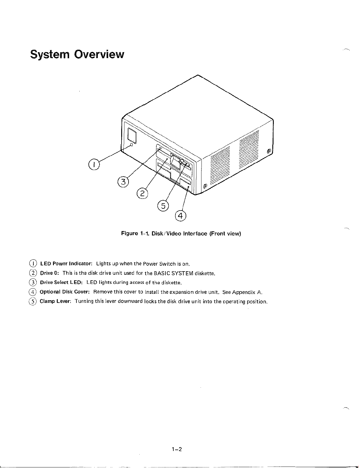
Figure 1-1. Disk/Video Interface (Front view)
CD
LED
Power Indicator: Lights up when
mDrive 0: This
(})
Drive Select LED: LED lights during accessofthe
CD
Optional Disk Cover: Remove this covertoinstall
is
the
disk drive unit used for
the
Power Switch
the
o Clamp Lever: Turning this lever downward locks
is
on.
BASIC SYSTEM diskette.
diskette.
the
expansion drive unit. See Appendix
the
disk drive unit into
the
A.
operating position.
1-2
4
5
6
Figure 1-2. DiskiVideo Interface (Rear view)
CD
AC Power Cord: Supplies AC power sourcetothe
G)
PowerSwitch:
CD
Fuse Holder: Contains a fuse. Remove
(±)
Video
Monitor
G)
Home TV Terminal: ProvidesRFoutput
TV
home
@)
Channel 3/Channel 4 Exchange
for Australia), whicheverisnot
(j) System Bus Connector: Connect
Turn
this switchonto supplyACpower to the Disk/Video Interface.
Terminal:
set to this terminal using
Connect
usedinyour
your
theTVcable and switch box supplied.
Switch*"':
the
system bus connectorofthe
3
2
Disk/Video
theACcord from
video
monitor
modulated to Channel 3orChannel 4*ofthe
Select either Channel 3 or Channel 4 RF
area.
for a80x25or40x25line display.
Interface.
theACreceptacle while inspecting/replacing
Portable Computer using
7
the
fuse.
TV
frequency. Connect your
output
(ChannellorChannel 2
the
attached cable.
~
Channel 1orChannel 2 'for Australia version.
Channel 36 UHF signal for UK/Belgium version.
""_.
Deleted for UK/Belgium version.
1-3
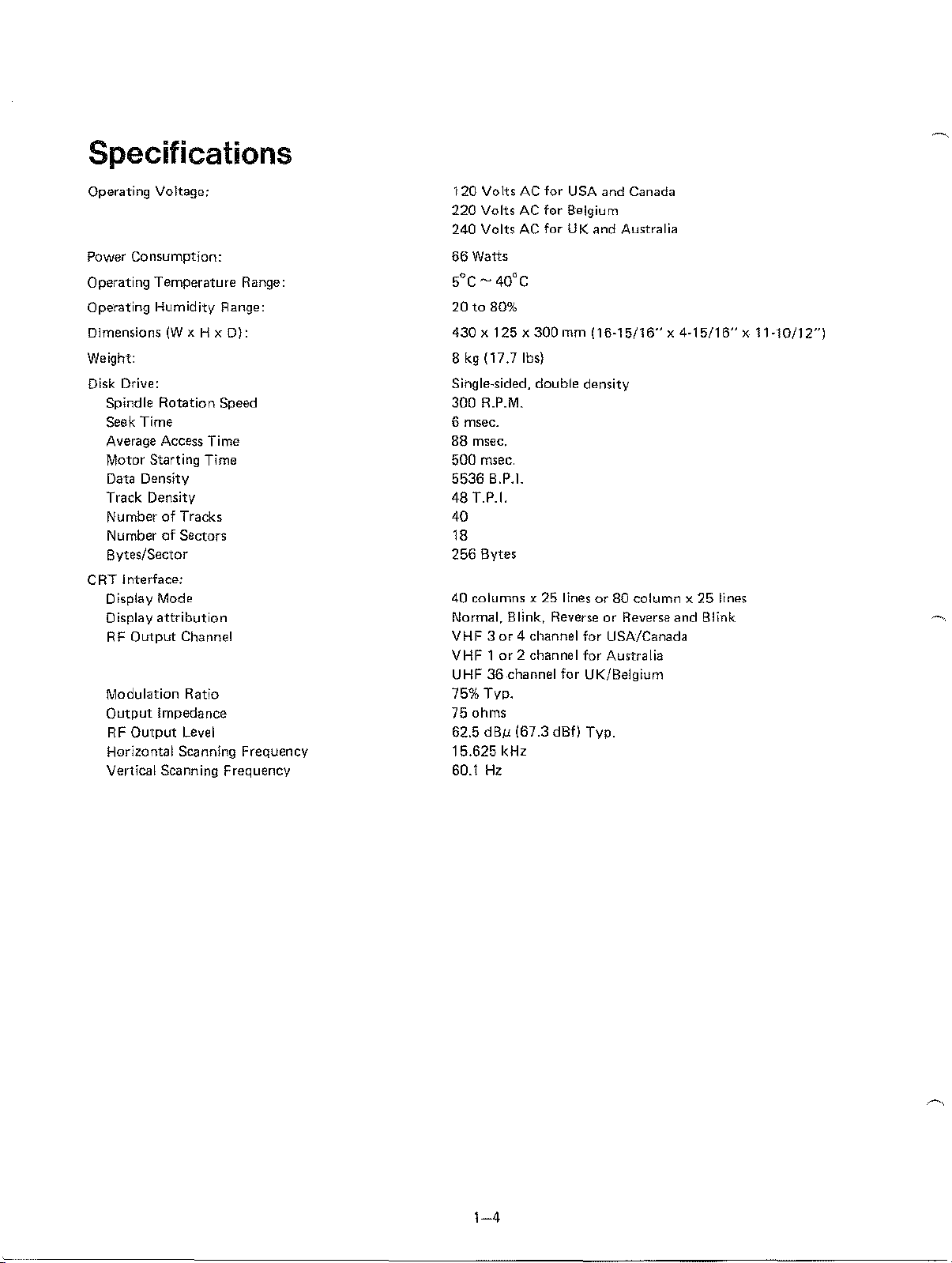
Specifications
Operating Voltage:
Power
Consumption:
Operating
Operating Humidity Range:
Dimensions(Wx H x O):
Weight:
Disk
Spindle
Seek Time
Average Access Time
Motor Starting Time
Data Density
Track Density
Number
NumberofSectors
Bytes/Sector
CRT
Display Mode
Display
RF
Modulation
Output
Horizontal Scanning Frequency
Vertical Scanning Frequency
Drive:
j nterface;
Output
RF
Output
Temperature
Rotation
of
attribution
Speed
Tracks
Channel
Ratio
Impedance
Level
Range:
120
Volts AC for USA
220
VoltsACfor
240
VoltsACfor UK and Australia
66
Watts
~
40°C
S"C
20to80%
430x125x300
8 kg
(17.7lbs)
and
Canada
Belgium
mm
(16-15/16"x4-15/16"x11-10/12")
Single,sided, double density
300 R.P.M.
6 msec.
88
msec.
500
msec.
5536
B.P.I.
48
T.P.1.
40
18
256
Bytes
40 columns x 25 linesor80 column x25lines
Normal,
VHF3or
VHF1or
UHF36channel
75%
75 ohms
62.5
15.625
60.1 Hz
Typ.
dBti
Blink,
4 channel
2 channel
(67.3
kHz
ReverseorReverse
for
USA/Canada
for
Australia
for
UK/Belgium
dBf)
Typ.
and
Blink
1-4
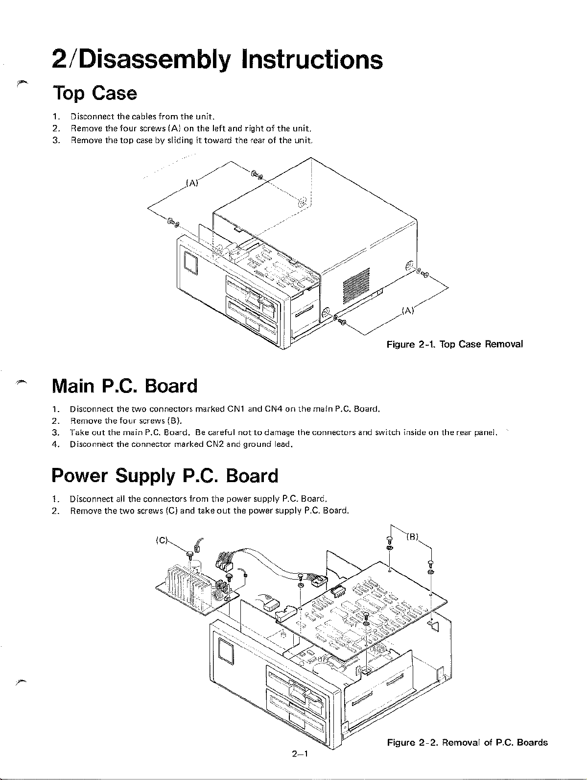
2/Disassembly Instructions
Top Case
1. 0 isconnect
2. Remove
3. Remove
the
the
Main P
the
cables from
four
screws (A)onthe
top
case by slidingittoward
.C.
Board
the
unit.
left
and
rightofthe
the
rear of
the
unit.
unit.
Figure 2
-1.
Top
Case Removal
1. Disconnect the two connectors marked eN1 and CN4onthe
2. Remove the
3.
Take
4. Disconnectthe connector marked CN2 and ground lead.
out
four
screws (B).
the
main P,C. Board. Be careful
nottodamage
the
Power Supply P.C. Board
1. Disconnect
2. Remove
all
the
two screws
the
connectors from
{C)
and take
the
power supply P.C. Board.
out
the
power supply
main P.C. Board.
connectors
P.C.
Board.
and
switch insideonthe
rear panel.
2-1
Figure
2-2.
Removal of
P.C.
Boards
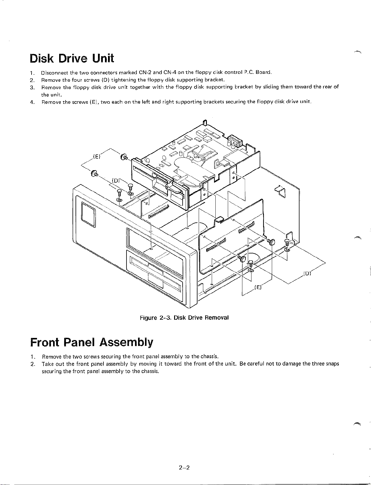
Disk Drive Unit
1. Disconnect
2. Remove
3. Remove
the
unit.
4. Remove
the
two
connectors marked eN-2 and
the
four screws
the
floppy disk drive unit together
the
screws (E), two each on
(0)
tightening
tr
CNAonthe
the
floppy disk supporting bracket.
with
the
floppy
the
left and right supporting brackets securing
floppy disk control P.C. Board.
disk supporting bracketbysliding them
the
floppy disk drive unit.
toward
the
rear
of
Figure
Front Panel Assembly
1.
Remove
2. Take
securing
out
the
the
the
two
front
front
screws securing
panel assemblybymoving it
panel assemblytothe
the
front
chassis.
panel assemblytothe
2-3.
Disk Drive Removal
toward
the
frontofthe
chassis.
unit.Becareful nottodamage
{D{
the
three snaps
2-2
3/Preventive Maintenance
To
ensure
the
proper
operationofthe
of
the
cleaning
Radio Shack's Universal Disk Drive head cleaning kit for S-1/4-lnch disks works well for this purpose. The kit includes
special cleaning disks
magnetic recording head.
and
one
bottle
Cleaning the Head
To
clean
the
magnetic head, use a lint-free
carefullytoremove all accumulated oxide and dirt.
CAUTION:
other than 91% Isopropyl alcohol may damage the head.
Extreme care
Rough or abrasive
must
be exercisedtoprevent
Adjustment
Disk/Video Interface,
of cleaning solution.
clothorcotton
cloth
should
notbeusedtoclean the magnetic recording head.
the
head
the
from
being damaged (do
only
scheduled preventive maintenance requiredisperiodic
swab moistened with 91% Isopropyl alcohol. Wipe
Useofcleaning solvents
not
scratch or strike
the
head).
the
two
head
This section describes
to
system
the
the
Appendix
diskette.
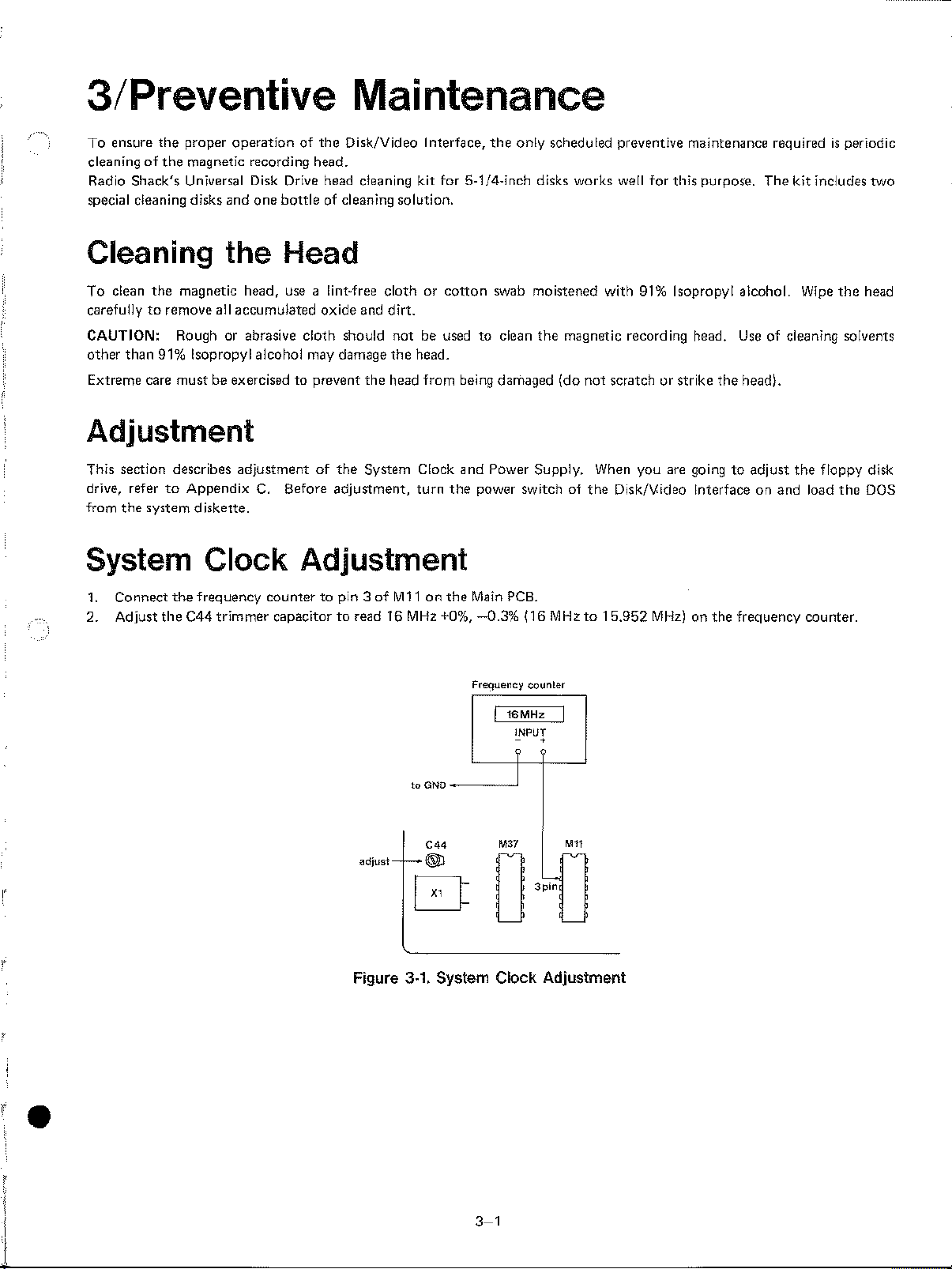
Clock
frequency
C44
trimmer
drive, refer
from
the
System
1.
Connect
2.
Adjust
adjustmentofthe
C.
Before
adjustment,
Adjustment
countertopin3of
capacitortoread16MHz
System Clock
turn
Mllonthe
to
GND
adjust
and
Power Supply. When you are goingtoadjust
the
power switch of
Main PCB.
+0%,
-0.3%
Frequency
o
16MHz
INPUT
?
--ll
MO<
(16
MHzto15,952
counter
•
3pin
-
the
Disk/V.ideo Interfaceonand
MHz)onthe
the
floppy disk
load
the
frequency counter.
DOS
J
Figure 3·1. System Clock Adjustment
•
i
I
3-1
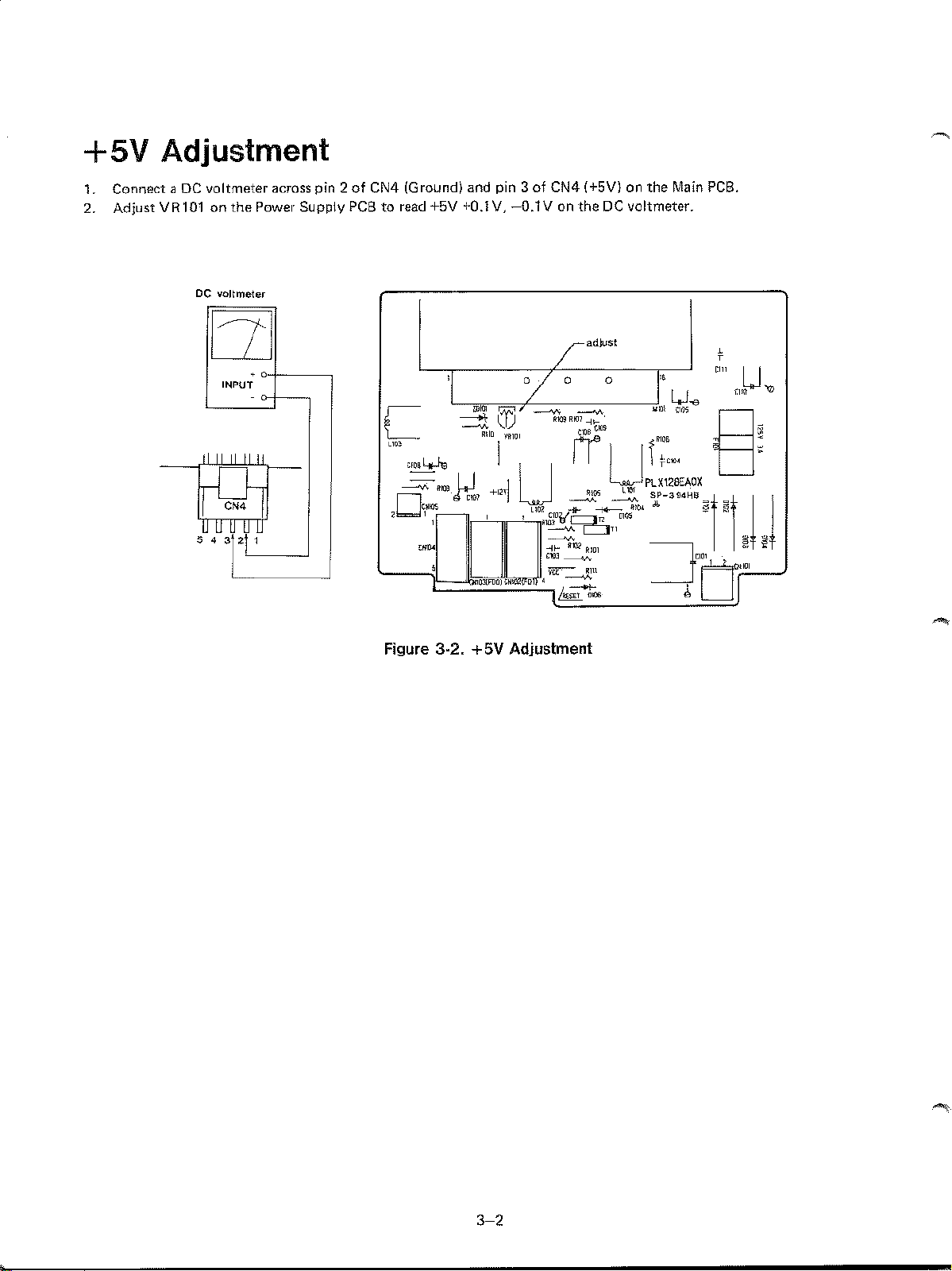
+5V
Adjustment
1. Connect a DC voltmeter
2. AdjustVR101onthe
DC
voltmeter
OJ
• 0
INPUT
"
'"
'"
~4
5 J4U3
!
'!
'
across
pin 2ofCN4
Power Supply
(Ground~
PCBtoread +5V
and pin 3ofCN4 (+5V) on
+0.1V,-0.1
V on
theDCvoltmeter.
/ad)US!
the
Main
PCB.
Figure 3-2.
+5V
Adjustment
3-2
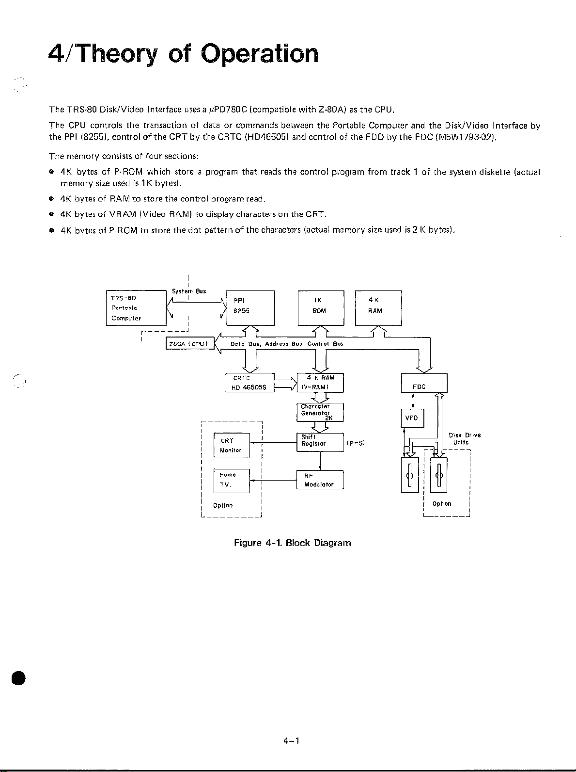
4/Theory
of
Operation
The TRS-80 DisklVideo Interface uses a pPD780C (compatible with Z-80A)asthe
The
CPU
controls
the
PPI
(8255),
The memory consists of four sections:
•
4K
bytesofP-ROM which
memory size usedis1K bytes) .
• 4K
bytesofRAMtostore
e
4K
bytesofVRAM
e
4K
bytes of P-ROM to store
the
transactionofdataorcommands
control
TRS~60
Portable
Computer
afthe
CRT
by the
CRTe
(HD46505) and controlofthe FDDbythe
store
a program
the
control
(Video RAM)todisplay characters on the CRT.
the
Systgm Bus
r
,
- -"
Z80A
program read.
dot
patternofthe
,
,
,
(CPUl
'"
8255
K Doto
that
reads
characters (actual memory size usedis2 K bytes),
."
BUS,
Add.ess
between
the
control
8us
the
Portable
program
"
ROM
<,
Cont.ol Bus
11 11
CRTCI==:>f
HD
46505$
~-------,
, ,
I
CRT
Monito' I
,
IHome
"
OpTion
________
I
I
,
,
,
,
,
,
,
,
,
I
,
,
J L
4 K
RAM
1I,'-RAMI
"'-J.
Chorocter
Gene.g!o.
"
"'-J.
Shift
Re~l",e.
j
ModulO-lor
"
lP-S)
CPU.
Computer
from
track 1 of
"
,,"
n-
and
FOG
eo'
8
0
,
,
,
fr,fr
,
,
~
,
,
,
the
Disk/Video Interface by
(M5W1793-C2).
the
system
diskette
I
Isk D.lve
0
Unit.
--,
--
,
,
,
,
,
,
,
--"
,
,
,
,
-
OpTion
____
(actual
•
Figure 4-1. Block Diagram
4-1
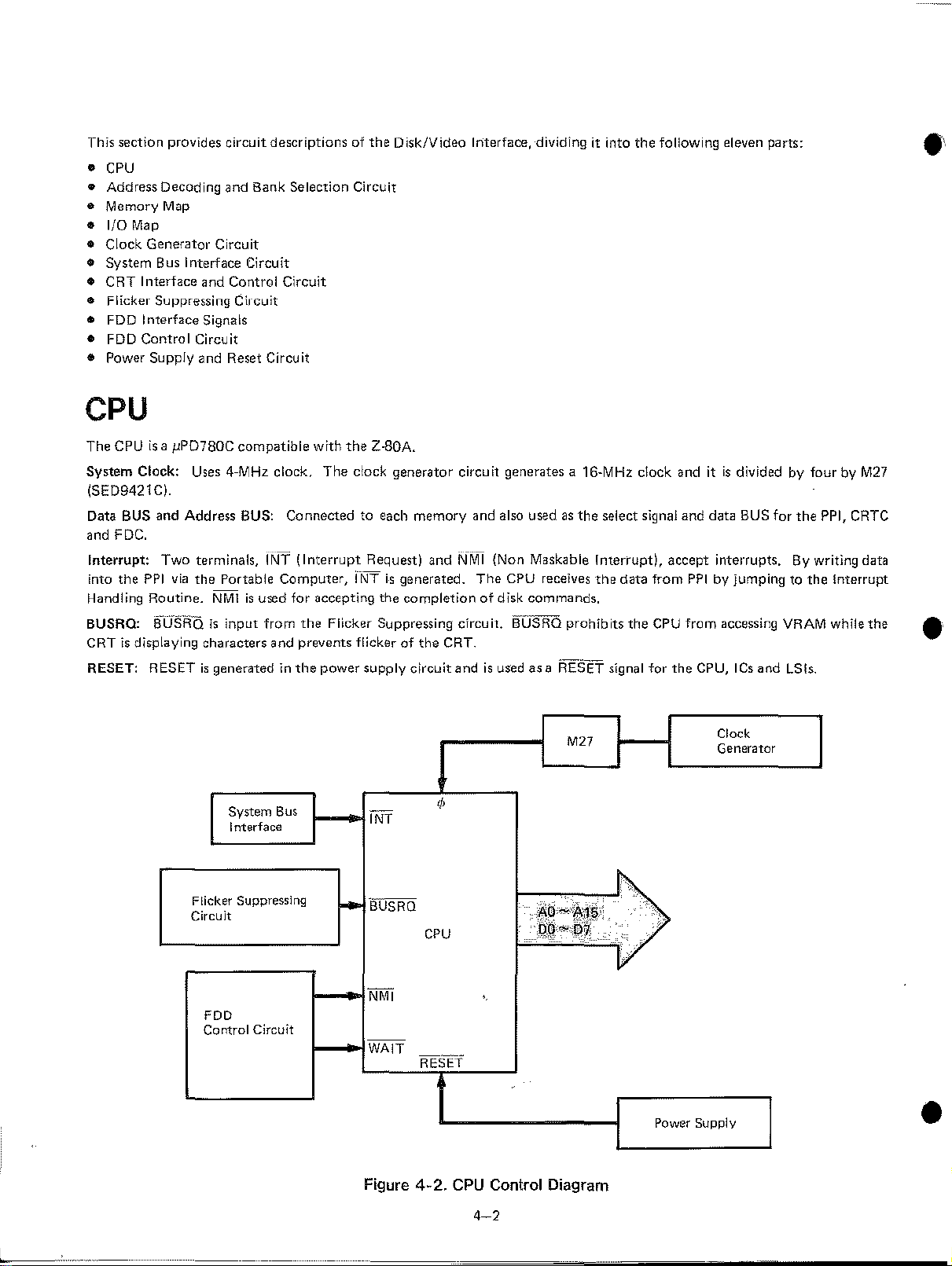
This section provides circuit descriptions of
the
0 isk/Video Iriterface,dividing it into the following eleven parts:
•
CPU
• Address Decoding and Bank Selection Circuit
• Memory Map
• I/O Map
• Clock Generator Circuit
• System Bus Interface Circuit
• CRT
• Flicker Suppressing Circuit
• FDD Interface Signals
• FDD Control Circuit
• Power Supply and Reset Circuit
Interface and Control Circuit
CPU
The CPUisa j1PD780C compatible
System Clock: Uses 4-MHz clock,
(SED9421C).
Data BUS and Address BUS: Connected
and FDC.
Two
Interrupt:
into the
Handling Routine.
BUSRQ:
CRT
RESET: RESET
PPI
is
displaying characters and prevents flickerofthe
terminals, INT(Interrupt
via
the
Portable Computer, (NTisgenerated.
NMIisused for accepting the completionofdisk commands.
SUSRQ
is
input from
is
generated in
with
the
Z-80A.
The
clock generator circuit generates a 16-MHz
to
Request) and
the
Flicker Suppressing circuit.
the
power supply circuit andisused as a
each memory and also usedasthe
i\fMl
(Non Maskable Interrupt), accept interrupts.
The
CPU receives
EfUSRO
CRT.
prohibits
RESET
dock
and itisdivided by four by
select signal and data BUS for
the
data
from
PPI
by jumpingtothe
the
CPU
from accessing VRAM while
signal for
the
CPU,
ICs
and LSls.
the
PPI, CRTC
By
writing data
M27
Interrupt
the
•
•
System
Flicker Suppressing
Circuit
FDD
Control Circuit
Bus
Interface
~
INT
'BUSRQ
--
NMI
--
WAIT
Figure
q,
CPU
RESET
4-2.
,
CPU
Control Diagram
'2"
M27
L'L'
Clock
Generator
<
Power
Supply
•
---------------------------------,--------
• Address Decoding and Bank Selection Circuit
M31
and
M38
determine memory address decoding. M31 decodes
and
M36l,
ARAM
The
outputof20inM16 selects BANK switching. At power-on, M16 receives
that
so
01ofthe
the
data bus to
(M23) and
program starts from address
"H",and
CRAM
the
(M9).
BANK1is
COOOHinthe
selected.
ROM. After
A15,
that,
A14
and A13, and selects ROM (M40), RAM (M28
the
RESET signal and
the
CPU
assigns STS as
BANKOisassigned
the
110
Port and sets bit
•
RFS'i-l
MREQ
m
A15 3
A14 2
A13
01 3 2
_.-
STSWR
RESET
6
1G
--
4
2GA
5
2GE!
M31
C
8
1
AGND
~
2D
elK
9
-
'13
-
Y6
Y7
V"
)'6
Vc
M16
1 J
YO
Y1
Y2
Y4
Y5
c
20
15
14
13
12
11
10
elK
9
7
NC
NC
NC
NC
NC
ARAM
CRAM
All
A12
15
13
14
M7
G
A
8
12
vr
v"
M38
GNO
J,-
BA'N'k6
BANK""
YO
'11
-
Y2
Y3
13
...d
12
9
...;,j
10
12
11
10
9
M34;
M34
NC
NC
11
8
,r
M28
M40 (p.
M36(R
(RAM
ROM)
cl~
AM1)CE
2)
CE
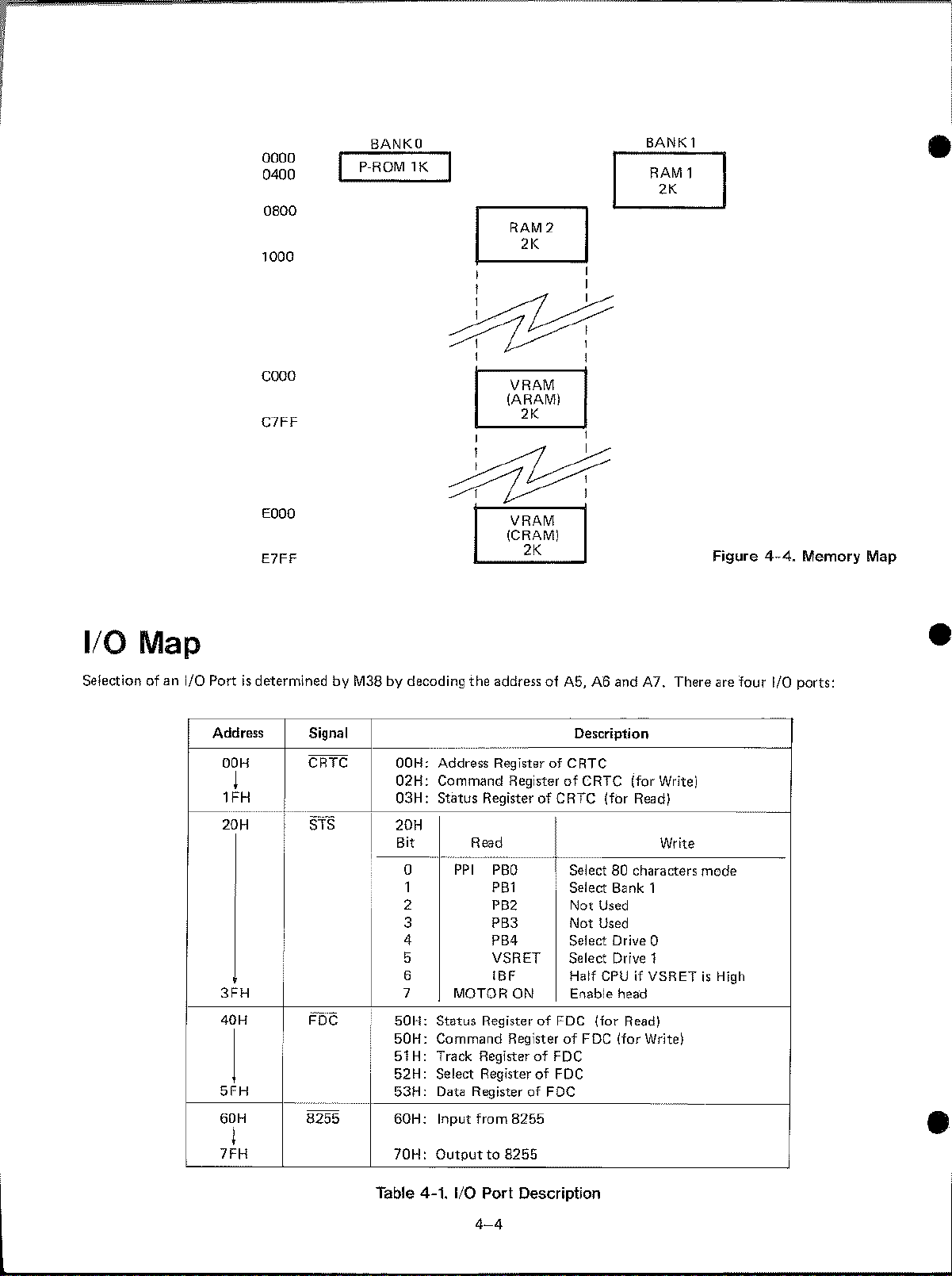
Memory Map
The DisklVideo Interface uses two 4K-byte P-ROMs and four 2K-byte Static
At power-on,
A10 and
Another
assigned for
Two other
which stores datatoreverse and blink characters.
• A P·ROM for
system disketteisbeing read,
the
Ali
P-ROMisusedasa character generator and accessed by
AAMs
combinationisswitchedtoRAM2
Figure
the
P·ROM
are connectedtoground through A25 and A28, memory
the
control program.
are
CRAM
the
program and
4-3.
Address Decoding and BANK Selection Circuit
programisusedtoload
(Character
RAM1
the
combinationofRAM2
RAM),
are switched by
and
BANK1
the
control program from
which stores datatodisplay on
the
BANK
and
BANKO
RAM1.
4-3
RAMs.
the
system diskette,
is
1024 bytes.
the
CRTC. Two 2K-byte
the
CRT, and
selection circuit. At power-on and while track 1 of
P-ROMisselected. After
RAMs,
the
butasthe
RAMi and RAM2, are
ARAM
system has been read,
address codes
(Attribute
RAM).
the
.----------------------~
-
0000
0400
0800
1000
CODO
C7FF
EDOO
E7FF
BANKO
P-ROM 1K
~
L..:..:.-J
I I
~
~
I I
VRAM
(ARAM)
2K
VRAM
(CRAM)
2K
~
~
BANKl
Figure
4-4.
Memory Map
•
I/O Map
Selection ofanI/O PortisdeterminedbyM38bydecoding
Address
DOH
j 02H:
1FH
20H
3FH
40H
5FH
GOH
j
7FH
Signal
eRTC
S1'S
FO'C
8255
DOH:
03H:
20H
Bit
0
1
2 PB2
3 PB3 Not Used
4 PB4 Select Drive 0
5
6
7
50H:
50H:
51H:
52H: Select Register
53H: Data Register
......
60H:
70H:
---------- ---------'''-
Address RegisterofeRTC
Command
Status
""'-'-
Status
Command
Track RegisterofFDG
Input from
Outputto8255
the
addressofA5, A6 and A7. There are
Description
RegisterofCRTC
Register
Read Write
PPI
MOTOR
RegisterofFOG
of
CRTe
PBO
PB1
VSRET
IBF
I
ON
RegisterofFOG
of
FOC
of
FOe
8255
Select80characters mode
Select Bank 1
Not Used
Select Drive 1
Half
Enable head
(for
(for
Read)
CPUifVSRETisHigh
(for
Read)
(for
Write)
Write)
,~""
four
----
•
1(0 ports:
•
Table 4-1. I/O
Port
4-4
Description
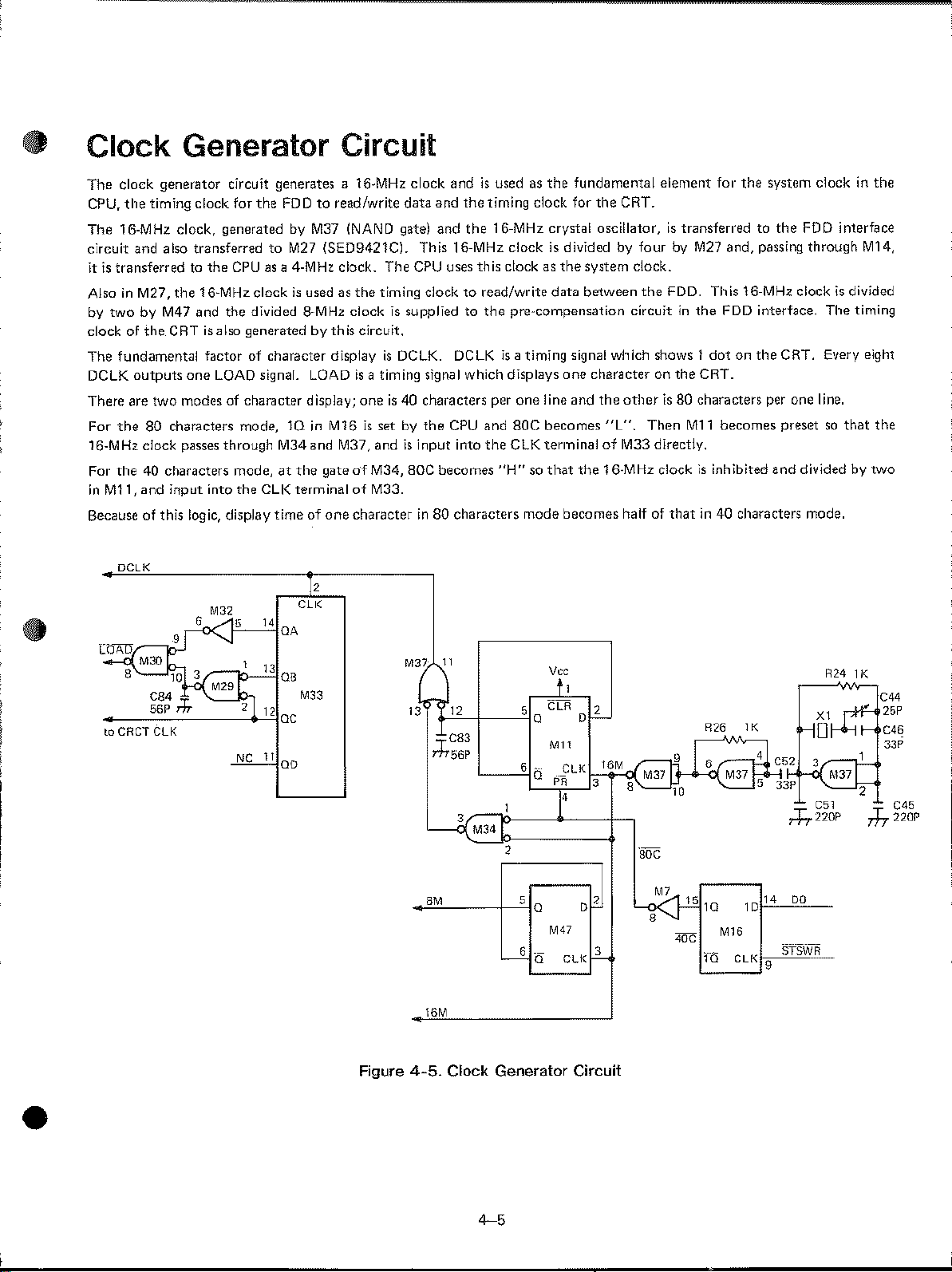
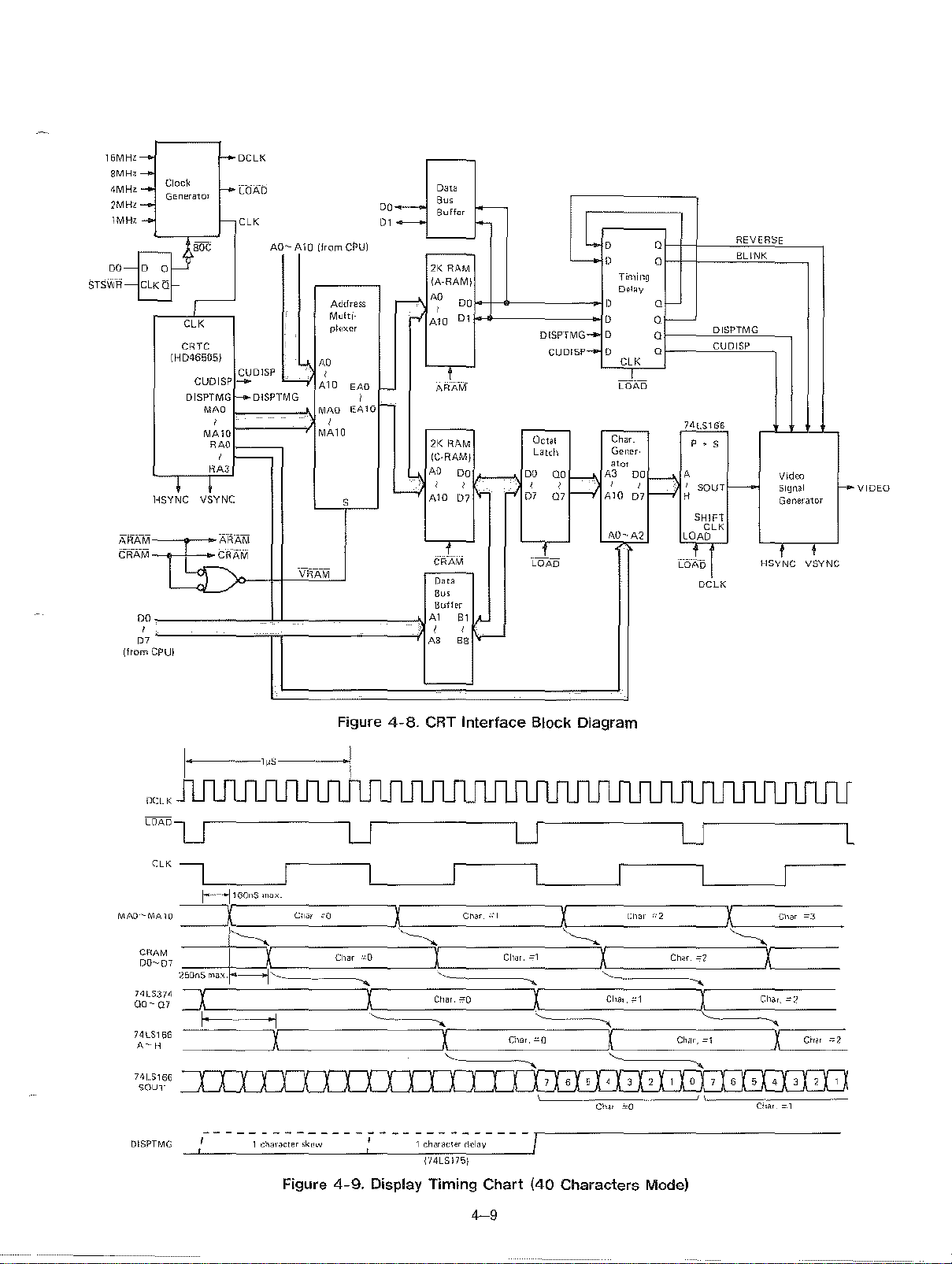
• Clock Generator Circuit
The
clock generator circuit generates a l6-MHz clock andisusedasthe
CPU,
the
•
timing clock for
The l6-MHz clock, generated by
circuit
and also transferredtoM27 (SED9421C). This
it
is
transferred to
in
Also
by
clock of
The fundamental factor of character display
DCLK
There are
For
16-MHz ciock passes through
For
in
Because of
M27,
twobyM47 and the divided 8-MHz clockissuppliedtothe
the
outputs
two
the
80
the
40 characters mode,atthe
Ml1,
and
DClK
to CRCT
ClK
the
the
l6-MHz clockisused as
CRT isalso generatedbythis circuit.
one
modes of character display;
characters mode, 1QinM16isset by
input
into the
this logic, display
G
the
FDDtoread/write
M37
(NAND gate) and
CPUasa 4-MHz clock. The
the
lOAD
M32
signal.
ClK
5
2
NC
lOADisa timing signal which displays
M34and
timeofone
14
0A
13
08
12
0C
11
00
M37, andisinput
gateofM34,
terminalofM33.
characterin80
2
ClI<
M33
data
CPU
timing clocktoread/write
is
DCLK. DCLKisa timing signal which shows 1
oneis40
BOC
M37
"
fundamental element for
and
the
timing clock for
the
l6-MHz crystal oscillator,istransferredtothe
l6-MHz
uses this clock as
characters per
the
CPU
into
becomes
characters mode becomes half of
n
clockisdividedbyfourbyM27 and, passing
the
system clock.
data
between
pre-compensation circuitinthe
one
one
line and
and
BOC
becomes
the
elK
terminalofM33 dIrectly.
"H"sothat
the
Vee
,
ClR
Mn
PR
D 2
,
"
C83
Jr
56P
3
C:l<>----''---+_
M34
5 a
6 b
2
the
CRT.
the
FDD. This l6-MHz clockisdivided
FDD interface. The timing
dotonthe
characteronthe
the
otheris80
"l".
Then
16-MHz clockisinhibited
CRT.
characters per one line.
Mll
becomes presetsothat
thatin40
the
system clock in
FOD interface
through
CRT. Every eight
and
dividedbytwo
characters mode.
R24 1K
I
f-'~
e51
220P
r+r
the
M14,
the
r-+
C44
25P
046
33'
•
Figure
8M
>OM
4-5.
Clock Generator Circuit
5 Q
6 Q
4-5
elK
D'
M7
15
8
3
'DC
10
f6
1D
M>O
CCK
14
9
DD
STSWR
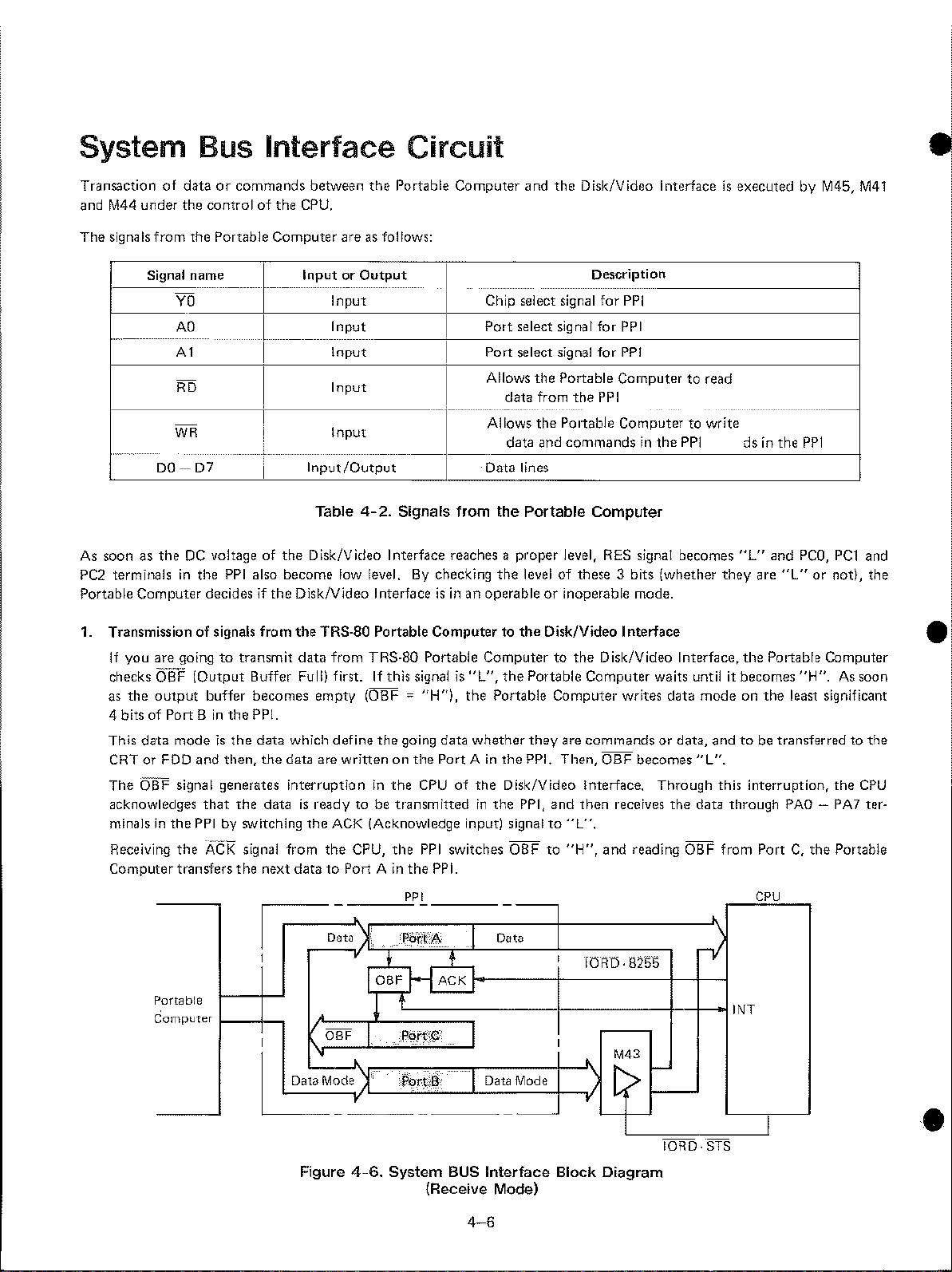
System Bus Interface Circuit •
Transactionofdataorcommands
and M44
The
under
signaIsfrom
Signal name
the
controlofthe
the
Portable
------------
Computer
1
__________
-----
YO
AD
Al
-
RD
-
WR
I
As
soon as
PC2 terminalsinthe
Portable
1. Transmission of signals
If
checks
as
4 bits
This
CRTorFDD
The
acknowledges
Computer
00-
the
DC
Computer
you
are goingtotransmit
O'i3F
the
output
of
PortBin
data
modeisthe
OSF
signal generates
minals
in
the
Receiving
the
transfers
D7
voltageofthe
decides if
(Output
buffer
and
that
PPI
A'CK
I
-------------
I
i
PPI
also
become
the
from
Buffer Full) first.Ifthis
becomes
the
PPI.
data
which
then,
the
data
interruptioninthe
the
dataisready to be
by switching
signal
from
the
next
between
CPU,
the
are
as tollows:
Portable
Computer
and
the
Disk/Video Interfaceisexecuted
-
lnputorOutput
Input
Input
Input
Input
Input
Input/Output
Table
4-2.
Signals
Disk/Video Interface reaches a
low level, By checking
Disk/Video Interfaceisinanoperableorinoperable mode.
the
TRS-SO
data
empty
are
the
the
datatoPort Ainthe
Portable
from
TRS·8D Portable
(OBF
define
the
writtenonthe
ACK
(Acknowledge input) signal
CPU,
Computertothe
signal
'"
"H"),
going
CPU
transmittedinthe
the
PPI
PPI.
Chip select signal
Port
Port
I
Allows
Allows
Data lines
from
Computertothe
is
"L",
the
data
whether
PortAin
o'f
the
switches
select signal
select signal
the
data
from
the
data and commandsinthe
the Portable Computer
proper
the
levelofthese 3 bits (whether
the
Portable
Portable
they
the
PPI.
Disk/Video Interface,
PPI,
OSFto"H",
Description
for
PPI
for
PPI
for
PPJ
Portable
Portable
level, RES signal becomes
Disk/Video
Computer
are
Then,
and
to
"L",
Computertoread
the
PPI
Computertowrite
Interlace
Disk/Video Interface,
Computer
commandsordata,
OBF
then
and
waits until it becomes "H".
writes
becomes
Through
receives
reading OSF from PortC,the
PPI
data
the
"L".
data
ds in
the
"L"
and
they
are
"L"
the
Portable Computer
modeonthe
andtobe transferredtothe
this interruption,
through
by M45,
M41
-
ppj
PCO,
PC1
and
or
not),
As
soon
least significant
the
CPU
PAD
- PA7 ter-
Portable
the
•
Portable
Computer
f--+--,
~
- -
-"
Data
•
OBF [
-"
ala
Mode
- -
Figure
PPI
~':,
'eo",,,,
'-'-;J-@
IOBF
[
ACK
T
X'
'PCin;g;:'
?0,\50
[
I Data
,
4-6.
System
BUS
(Receive Mode)
4-6
---,
Data
Mode
--
Interface
,
fORD·8is'5
,
t?
Block Diagram
lORD·
rY
STS
CPU
INT
i
•
•
2.
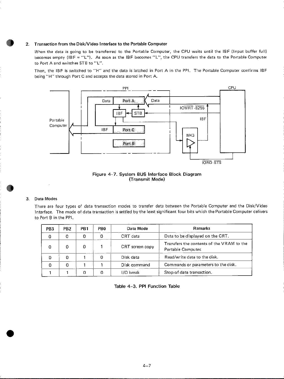
Transaction from the Disk!Video Interlacetothe
When
the
dataisgoingtobe transferredtothe
becomes empty (ISF
to
Port A and switches STS
Then,
the
ISFisswitched
being
"H"
through
'"
"L"),
Port
C and accepts
As soon as
to
"L".
to
"H"
and
the
Portable Computer
Portable Computer,
the
ISF becomes
the
dataislatchedinPort Ainthe PPI. The Portable Computer confirms ISF
data storedinPort
"L",
A.
the
the
CPU
CPU
waits until the ISF (Input buffer full)
transfel's
the
datatothe
Portable Computer
•
Portable
Computer
3. Data Modes
There are four typesofdata
Interface. The mode
to
Port Binthe PPJ.
fr==o'"
I
I
IBF
I
~I
IBF STB
I
I
L_
Figure4-7. System BUS Interface Block Diagram
transaction modestotransfer data between
of
data
transactionissettled by
PPI
-
poihl\.
:Rottiei:'
i~~:ty~)i
-
(Transmit Mode)
--
,
,K
Data
'
I
I
_J
the
least significant four bits which
I
I
L..
IOWRT·8255
IBF
f---
[?
IORD·STS
the
Portable Computer and
the
CPU
1
the
Disk/Video
Portable Computer
del
ivers
•
f--~PB=3--+_P~B~2--1_P_B_'_J~B?
1
__
o=----+_~o_+--=o-L
o
o
°
1--
-+--0-+-,
0
1--o-+-co,-···.J
,
i"
"
'1''''''0'''-1
0'
...
I
...
Eata_M_O_d'
_,~,_~_~T
I I Transfers
CRT screen copy
________
Disk data ! Read/write datatothe
~o'1D'/iO-~~bc'::~k-0:~~~.
Table
4-3.
__
+
1__
data L
-+'
II
"'"
PPI Function Table
4-7
Remarks
..
~.~~~~?""~_:
Portable
Commandsorparameterstothe
Stopofdata
__
?.i,~played
the
contentsofthe
C~o~m",:,pu~t~'~I
transaction.
on
the
CRT.
VRAMtothe
disk.
~~-----1
disk.
--j
CRT
The
is
storedinthe
becomes
M9isthe ARAM
when
terminalsofM23
When
in
M18and assigns A3·A
On
the
Jines
M15
When the character display
ANOsthe
64
in
M2
the
zontal sync) signal generatedinCATeisalso input
input signals.
When using a CRT monitor, this composite video signal
to
61.25
controls switching of
Table
Figure
Figure 4·9 shows
Figure 4·11 shows
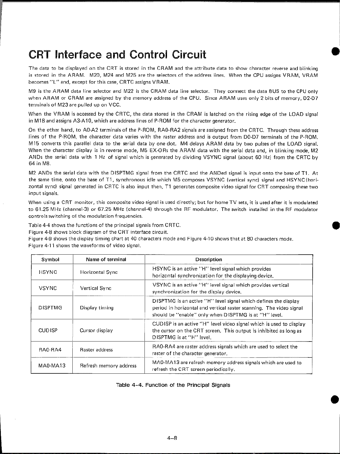
Interface and Control Circuit
datatobe displayedonthe
ARAM. M20, M24
"L"
and,
except
for
data
line selector and
ARAMorCRAM
are pulled up on vee.
the
VRAMisaccessed by
other
hand,toAO·A2 terminalsofthe
of
the
P·ROM,
converts this parallel datatothe
serial
data
M8.
ANDs the serial data with
same time,
4A
4·8
onto
MHz
(channel-3) or
shows
the
shows block diagramofthe
the
are
10,
the
character data varies with
with 1Hzof signal whichisgenerated by dividing V$YNC signal (about 60
the
baseofT1,
the
modulation frequencies.
functions of
display timing chartat40 characters mode and Figure 4·10 shows
the
waveformsofvideo signal.
CRTisstoredinthe
and
M25
are
the
this
case,
CRTe
assigns VRAM.
M22isthe
assignedbythe
the
CRTe,
which are address lines of p.
isinrevel'se mode,
the
DISPTMG signal from
67.25
MHz
the
principal signals from CRTC,
memory addressofthe
the
serial data by
synchronous idle whichM5composes VSYNG (vertical sync) signal and HSYNC (hori-
(channel·4) through
CRT interface circuit.
CRAM data line selector.
data storedinthe
P·ROM, RAO·RA2 signals are assigned
the
M5
EX-ORs
then,T1generates composite video signal for CRT composing these
CRAM and
selectorsofthe
ROM
raster address andisoutput
one
dot.
the
is
used directly;
the
attribute
address lines. When
CPU. Since
CRAMislatchedonthe rising edge of
for
the
character generator.
M4
delays ARAM databytwo
the
ARAM data with
GRTC and
the
the
ANOed signalisinput
but
for home TV sets, itisused after itIsmodulated
RF modulator. The switch installedintheRFmodulator
datatoshow
They
connect
ARAM
from
from
the
serial data and,inblinking mode,
thatat80
character
the
CPU assigns VRAM, VRAM
the
uses
only2bitsofmemory,
the GRTG. Through these address
00·07
characters mode.
reverse and blinking
data
BUStothe
the
terminals of
pulsesofthe
Hz)
from
onto
the baseofT1. At
LOAD
the
LOAD
the
CPU
02-07
P-ROM.
signal.
GRTG
only
signal
•
M2
by
two
•
of
Symbol Name
HSYNC Horizontal Sync
VSYNC
OISPTMG Display timing
CUOISP Cursor display
Vertical Sync
terminal
i DISPTMG
RAO-RA4
MAO-MA13
Raster address
Refresh memory address
Table
uuuu"''''.,
..........~..
HSYNC
horizontal synchronization
VSYNC
synchronization for the display device.
-----
DISPTMGisan active
period
should
CUOISP
the
RAO-RA4 are raster address signals which are used
..
.......
4-4.
rasterofthe
MAO-MA13are refresh memory address signaIswh ich are used
refresh
Functionofthe Principal
is
is
in
be
is
cursoronthe
the
Description
,
an active
an active
horizontal and vertical raster scanning. The video signal
"enable"
an active
is
CRT screen periodically.
"1-1"
"H"
only when OISPTMGisat
"H"
CRT screen. This
at
"H"
level.
character generator.
-
level signal which provides
fO!'
the
displaying device.
level signal which provides vertical
"H"
level signal which defines
level video signal whichisusedtodisplay
outputisinhibited as long as
--------
_
...
_-,,-,-,-""'-,~,-,-
Signals
"H"
the
level.
to
select the
display
to
•
4-8
Hl---{>
~H
Cloct<
~,-
GEnerato,
Hl_
H'
.....
r--~80C
- C C
co
-
STSWR
CLKQ
~
,----
"<
Cine
(HD46505)
CUDISP
DISPTMG
MAO
MAW
HSY~C
AYNC
'~;Ll
(from
00
,
CPUI
"
E5
4DCLK
r-<"
WAD
'"
CUDISP
-
__
DISPTMG ,
,
eM
,
-
eM
AO~
A10
e..,
VnAM
0","
00
01
(frQm
CPU)
Add"ss
Multi-
pl"xcr
M
,
AW
eM
fAl0
MM
,
MAlO
,
-
0",
...
--
Buffer
____
2K
RAM
lA-RAMI
M
~
,
AW
ARTjijiff
2K
RAM
IC-RAM)
M
,
--"I
AW
(j\~M
Dot'
"",
Buffor
,
"
AO
CO
"
co
"'
"'
eo
-
,
.,
SOUT
SHIFT
DCLK
DISPTMG
CUDISP
'"
REVERO;E
BLINK
'---<
HSytc
VideQ
Si~n.1
Generator
,
VSYNC
-
VIDEO
L
0 0
'---<
"
D 0
,
.....
,
~
......
C
C
M
"0
DISPTMG
CUDISP
Octol
Latch
co
GO
,
,
07
t--&-AD
m
Timing
Del,y
eLK
["dAD
Chof.
GQ"O"
ator
,
AO'-A2
co
,
-..,
---
m
"
,
f--
Q
Q
74l.$166
A
,
~
l.OAD
c6-A01.
,
'<-
D(:LK
ClK
I~~
74lS374
00-
01
74LS1ofl
A-·
H
7~1..s166
SOUl'
DiSPTMG
Figure
I--·,e----l
160
r"
'1
"S"'0'_
x X
~-----------------
Figure
4-9.
4-8.
CRT
Interface Block Diagram
u u
1_-----'
Cho,,"n
'-
,
----------,----------
1 oh"co",., ,Icl,y
1'14lS175i
Display
Timing Chart
1_-
~
~
'---------
(40
Cha,
Characters Mode)
u L
1_-
Ch"",_l
",---------1
"0
\
Ci,.,
X
Ch"
-_2
4-9
---
----0_5I'S-----.1
OCLK
w'"U,.------,U------,U,.----U'----;L
eLK,
'----
I I 1
__
14LS1li6
SOUT
DISP'I'MG
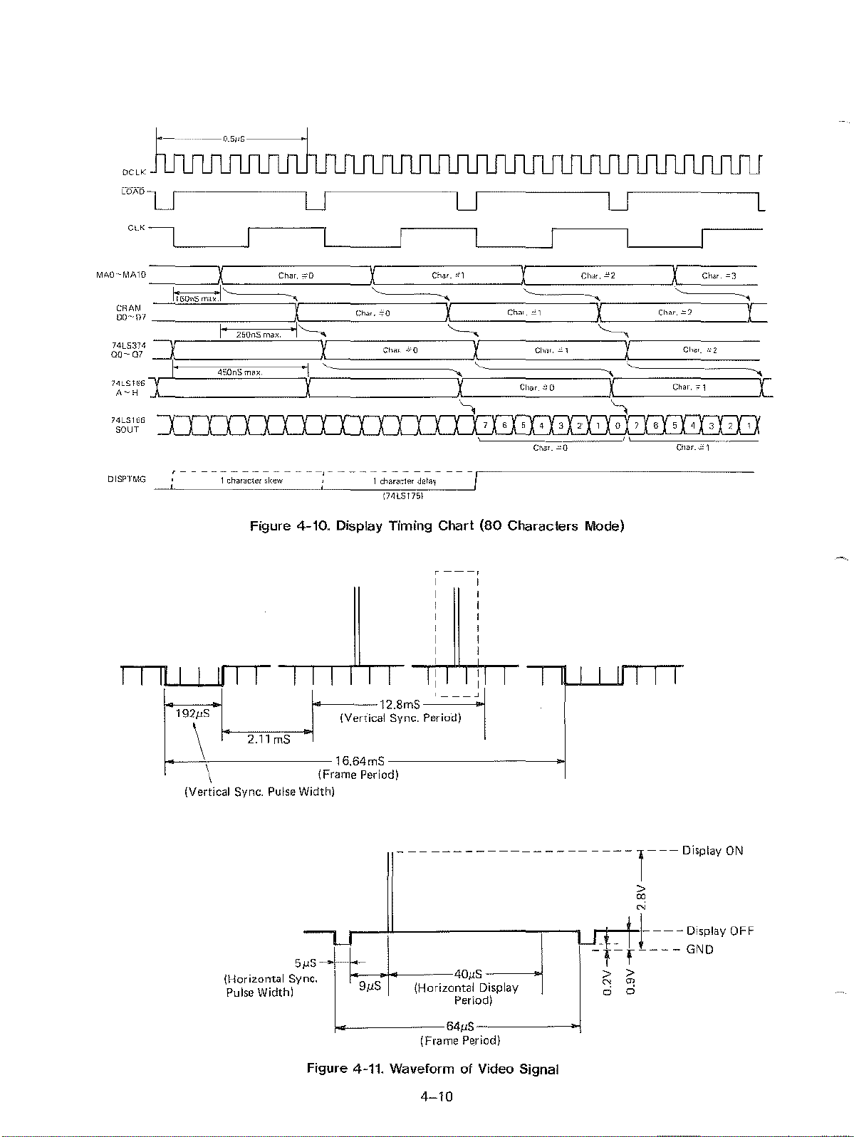
Figure 4-10. Display Timing Chart
192pS
\ 1---,;,-;.1'1
1---\-------16.64mS------------I
\ (Frame Period)
(Vertical Sync.
~
=m:S
Pulse Width)
4 3 2 6 5
(80
Characters Mode)
r
---,
I
I
,,--12.8ms-'-------~.,
(Vertical Sync. Period)
~
3
Cil1l'_·~1
~---~~------~
(Horizontal Sync. L
Pulse Widthl 9jJS (Horizontal Display
5"S~--~
Figure 4-11. Waveform
·-40pS-
64
--
(Frame Period)
4~1O
~
Periodl
5
11
--------1
of
Video Signal
------~-1---
>
ro
~
__
l---~Di;PlayOFF
-rr----
> >
C'!
0:
o 0
Display
GNO
ON
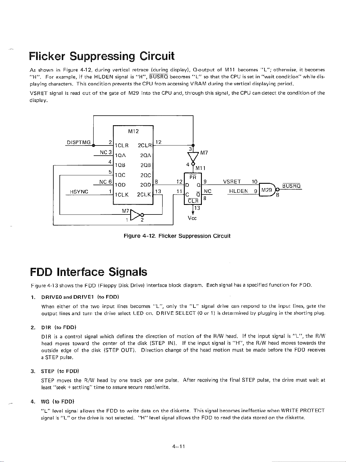
Flicker Suppressing Circuit
As
showninFigure
"H",
For
example,ifthe
playing characters. This
VSRET
display.
signalisread
4-12,
during
HLDEN
condition
outofthe
vertical
signalis"H",
prevents
gateofM29
retrace
the
M12
CPU
into
(during
BUSRQ
from
the
CPU and,
becomes
accessing VRAM during
display),
through
Q-output
"L"sothat
this
of
Mll
becomes
the
CPUissetin"wait
the
vertical displaying period.
signal,
the
CPU can
"L";
otherwise,itbecomes
condition"
detect
the
conditionofthe
whIle dis-
DISPTMG 2
FDD
Figure 4"13 shows
1,
Interface Signals
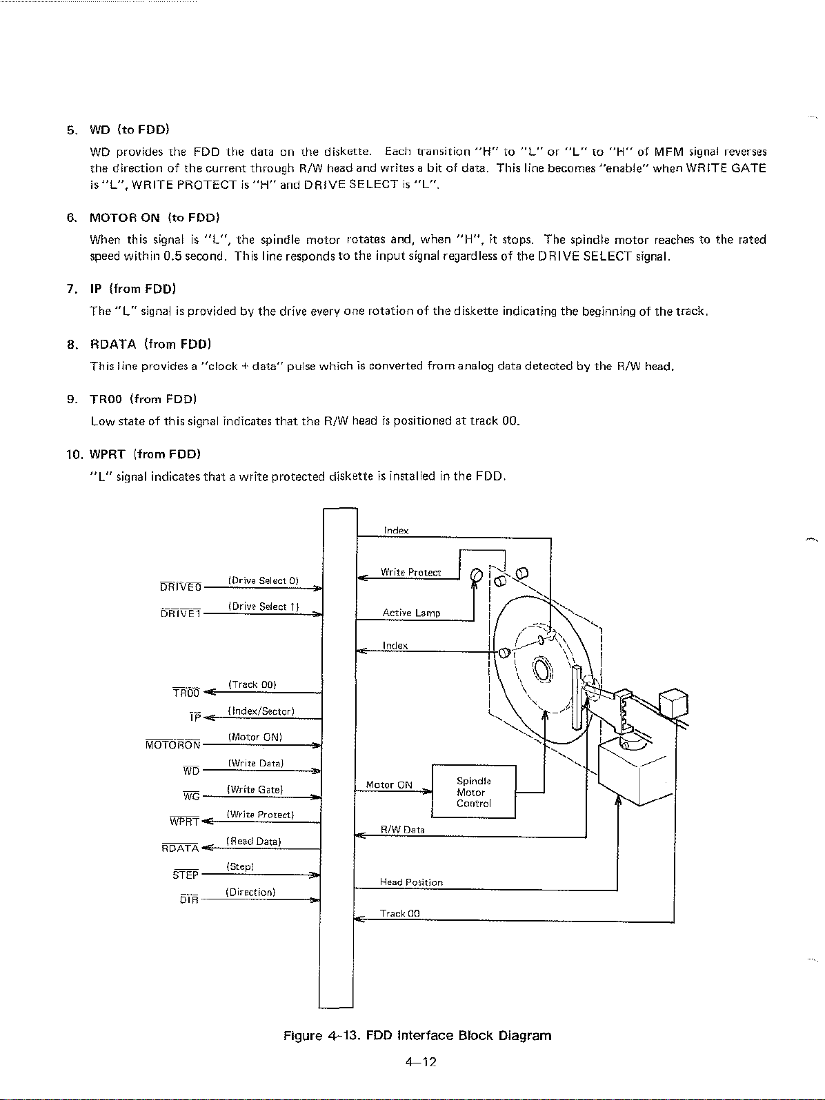
DRIVEO
When eitherofthe
output
and
lines
HSYNC
the
DRIVE1
and
turn
FDD
two
lelR
NC3
lOA
4
lOB
5
lOC
NC
6
100
1
lCLK
(Floppy
(to
the
Disk Drive) interface block diagram. Each signal has a specified
Fool
input
lines
drive select LED
20A
20B
20C
200
12
8
I-'-"
12
.-'-'
~
4 Ml1
PR
0
0
C 0
CLR
+13
V"
M7
9 VSRET 10
I-""'-
8
2CLR
2CLK
M7
;1/2
Figure 4-12. Flicker Suppression Circuit
becomes
on.
"L",
DRIVE
only
SELECT (0
the
"L"
signal drive can respondtothe
or1)is
determined
HLDEN
91
M29
by plugginginthe
BUSRO
B
function
input
for FDD.
lines, gate
shorting plug.
the
2.
OIR
DIRisa
head moves
outside
a STEP pulse.
3.
STEP
STEP moves
least
4.
WG
"L"
signal
(to
Fool
control
edgeofthe
{to
Fool
"seek+settling"
(to
FDO)
level signal allows
is
"L"orthe
signal which defines
toward
the
R/W headbyone
driveisnot
the
directionofmotionofthe
the
centerofthe
disk (STEP OUT). Direction changeofthe
timetoassure secure
the
FDOtowrite
selected.
disk (STEP
track
read/write.
dataonthe
"H"
IN~.
per
one
pulse. After receiving
diskette.
level signal allows
I'f
the
the
R/W
head.Ifthe
input
signal
is
"H",
head
motion
This signal becomes ineffective when WRITE PROTECT
FDOtoread
must
the
final STEP pulse,
the
input
the
R/W
head moves
be made before
data
storedonthe
signalis"L",
towards
the
FDD receives
the
drive must
diskette.
the
R/W
the
wait
at
5.
WO
(to
FOO)
WD
provides
the
directionofthe
is
"L",
the
FDD
the
dataonthe
current
through
WRITE PROTECTis"H"
diskette. Each transition
R!W
head and writes a bitofdata. This line becomes
and DRIVE SELECTis"L".
"H"
to
"L"or"L"
to
"H"
"enable"
of
MFM
signal reverses
when WRITE GATE
6. MOTOR ON
When this signal
speed within
7.
IP
(from FDOl
The
"L"
signalisprovidedbythe
8.
ROATA (from FOOl
This line provides a
TROD
9.
(from
Low
stateofthis signal indicates
10. WPRT (from
"L"
signal indicates
(to
FOO)
is
"L",
the
spindle
0.5
second. This line respondstothe
"clock+data"
motor
drive
everyone
pulse whichisconverted from analog data
Fool
that
the
Fool
that
a write pl"Otected disketteisinstalledinthe
DR
IVEa_--"I
D~c~i,"e"S~e"'
"C",,,O"'~..J
I"Otates
and, when
input
signal regardlessofthe DRIVE SELECT signal.
rotationofthe
R!W
headispositionedattrack 00.
-
Index
Active Lamp
"H",
it stops. The spindle
diskette indica'ting
detectedbythe
FDD,
the
beginning of
motor
R/W
reachestothe
the
track.
head.
rated
TFi'oo
WD
WPRT
RDATA
STEP
OrR
(Track 00)
~---'-=="'----I
_
_
,,'~Wc"'c,"cDe"~'~"''-_..J
{Write Protect)
~--"'==="-----I
(Read Data)
~====---I
_
_
"(S~''''P~I
(Dirsction)
-==="--~
-;..J
-
Figure 4-13.
Motor
ON
R!W
Data
Head
POSition
Track 00
FDD
Interface Block Diagram
Spindle
Motor
Control
4-12
FDD
Control Circuit
FDD cOntrol
1.
FOe (Floppy Disk Controller)
FOe
CPU.
Combining
the
Table 4-5 shows
circuit
consists of
To
detect
these
command,
consists
one
the
signals
read/write dataorrequestofstatus.
the
I--'---t--
l-~,~,
I--\-,c-
+_0_-1
I--
\--\-'---1--+,
1-1----'--+
of
FOe (M26), data separator (M27), pre-compensation
LSI (M26) and, using 0 BUS, transfers
selectionbythe
with
lORD
combinationofthe
AO
+!
_c
o , 0
o J
1 0 0 1 I Reading of
--+!
-C
,
1 I 1 0 Transfer of read
1 1
CPU, Y2
and
IORW signals, FOG identifies
signals:
Al
O
_+_
1 1
"'----j--,c---j
O
lORD
I----'C=---t- -
0 I 0 1__Rc'c'=dcin_g
,1
+----:0----:+'
----f-
-=----+---=
lOT
Table
output
signal (FOG) by
IOWR
0 Writing
-,
-r---:c
__
I
1_--=O
__
0-
4-5.
FOe Function Table
--
__
+_Writin
Writing
-+-
-1----'-'
commands
..
__
?ft~~_status
onto
-
R
eading 0
g
ont_o_'_h_etrack
_
onto
ransfer of write data
and
data
liD
port
the
signals
Description
the
command register
f k .
trac
the
sector register'
the
sector
data
circuit,
re,g':":':'
and
wait
control
correspondingtothe
decoder M38 and
from
the
CPUasto
regjst~r
_
---1
re,gc"c":'
__
-I
C
re···g·
,,-,-,-,
--l
----I
AD/A1
circuit.
FDD from
signa! are used.
whether
they
the
are
The
table
below shows
about
this LSI, refertothe
1791 usedinthe
Symbol
I---
--
DRQ
the
functional descriptionofthe
TRS-80 ModelIITechnical Reference Manual since this
FDC Printer Interface Boardofthe
Name
Data request
1
IRQ Interrup't
-
STEP
"
DI~:~tion
I-
EARLY Early
LATE
i
1-
Step
Late
I
HLD
I-
IP
-.
TROO
Head load
Index pulse
-----
Track
00
Input/Output
Output
Output
Output
Output
!
Output
,,,.-
Input
I
Output
Output
Input
principal terminals. I'f
Model II,
-
-
except
that
In
disk read mode,
in
the
data register.Indisk write mode, it indicates
data registerisemptY. DRQis
operation.
IRO becomes activeatthe
andisreset when the CPU reads
command.
----
Step pulse
-
High
means
This signalisused for write pre-compensation.
that
This signalisalso used for write prs·compensation. It indicates
This oUtput signal controls
the
output.
This input indicates
encountered.
This signal tells
trackOO. Active low.
output
level
means
that
the
headisstepping
the
write data pulse should be shifted eariy.
thatthe
FDD. The
wl'ite data pulse should be shifted late.
motor
the
you
wanttohave additional information
LSIisfunctionally identicaltothe
the
data
BUSistrueasopposedtoinverted.
Description
ORO
indicates
completion requestofcommand
..
_--
(Active high).
..
_-.
that
the
headisstepping in and low
mustberotatedbythis high
that
an index holeofthe
device
that
that
resetbythe
the
__
.-
out.
the
rotationofthe
the
headislocated
statusorwrites
the
dataisassembled
readorwrite data
---
-
that
the
It indicates
motor
level
diskette
on
the
..~--
-
--
level
--
of
is
-
4-13
j
Symbol
- -----
WPRT
--
DDEN
RClK
RG
RAWRD Raw read
WG
Name
Write
protect
Double density
mode select
Read clock
Read gate
Write gate
-
-----
f---
WD
RESET
Write data
Reset
Input/Output
Input
Input
Input
Output
Input
Output
Output
Input
low
level signalofthis input informs
drive
is
in write
starts, this signalissampled and an active low signal termi·
nates
the
current
status
bitinthe
This input determines
DDEN",O selects
This signalisused internally for
relationtothe
(RClK
This signal shows
syncfield
This input signal from
recorded flux transition.
This signal becomes active before disk write
occurs.
This signal consistsofdata bits and clock bits. It becomes
active for every flux transition .
Active low.
matically loads
not·ready"status
inputismade high,
unless readyisactive and
sector register.
highorlow)isnot important.
is
~
detected.
--------
I.
-"'-
..
I
Description
protect
command, and sets I
status registerisalso set.
double
raw read dataisspecified,
the
The
deviceisresetbythis signal and
"03"
bitisalso I'eset by this signal. When reset
the
device
state. Before disk write operation
RQ.
Write pr-otect
the
operation
density mode.
external data separat"lon
the
drive shallbelow for each
into
the
the
device executes restore command
the
modeofthe
the
data windoW. Phasing
but
operation
command register.
device loads
"01"tothe
the
that
that
the
device.
polarity
the
auto·
The
.~..~
-
2. Data
Separator
SE09421C
data (RDATA) read
·AD
from FDD
is
DATA
(SED9421C)
an
IC
which generates a
outofthe
Data
"1"
M21
Table
FDO. Figure
ClK
/
4-6.
Description of the Principal Terminals
data
Data
RD
4·14
ClK
DATA
window signal
shows
the
M27
5
SED·
9421C
7
6
that
functionsofthis
Data
"1"
Jl
)
DATA
WINDOW
ClK
nl-_---.JIL
M21
9
separates clock bits and data bits among the
IC.
Data
ClK
"0"
M26
FDC
----
8
27
26
RAWRD
RCLK
-
Figure 4-14. Data Separator
4-14
3.
Pre.compensation
This circuit adjusts timingofthe
be
shifted in writing since peakofthe
The
time availabletocompensate
In
Figme 4,15, FOC
terminals
of
Circuit
M46 becomes
write
data
delivered from FOGtothe
data
may shift during data reading, dependingontheir data pattern.
is
125
nanoseconds, i.e., one pulse width
outputsanEAR LYOrLATE signal, dependingonthe writing data pattern; then,
"H"
so
that
the
numberofflip-flops through which
FDO. This circuit compensates data which will
of
8
MHz.
WD
(write data) passesisdetermined.
DO,
01or02
-,
o e
---'
M(,g
E....::l
~
EWD
YODO6
0'
"
",
co
M'15
A
"
,
IEARLYModel
4. Wait Control Circuit
As
shown in
During read
executes a
At
this
reads
and WAIT becomes
The
CPU
time,
the
repeats
the
figure below, this circuit controls read/write
operation,
dummy
Pin-9
data from
the
-
9 0 D
M,j8
"
91112
~1
-""
5~
,
the
GPU
read
operation
o'f
M1
becomes
Foo
and
"H",
Then,
above procedures and reads
0
~
~
Q 0
M49
Q
~
Figure 4-15. Pre-Compensation Circuit
transfers a read
once setting
"L"
the
bufferis'filled
the
CPU
o 0
M41
I,
~
2EARLY
,
LATE
"
11
A4="L"
and
the
releases
we
8MH
commandtothe
and
CPU
enters
by
8 bits
"wait
condition"
the
data from the FOC coll'tinuously.
~~2
M",
~l
-
'WO
YODO6
"
co
"
M45
A
0
data
transaction between the
FOG
setting
FOC="L".
"wait
condition".Inthis condition,asSoon as
of
data,
ORO
becomes
and reads
~
'Q
M"
~l
,
I;-
"
,
ILATE
Mode)
A4="H"
"H",
the
data storedinthe
9-12
M"
Q
~3
,..--------,
~
0,
o 0 "
M"
-1
EARLY
LATE
e
"
sr;;--
WO
8
~M4~1:2
Q
1"1
L5
CPU
and
the
FOG.
and
FOC="L".
Q terminal oi' Ml becomes
Then, the
the
FoC.
Mel
CPU
FOC
"L"
ORO
M26
~
M~;~
_
...:£.¢
'C14",M~H:.:',-)
----01
3
eLK
~I"-
MI
Figure 4-16. Wait Control CirCUit
CPU
r-
d
9 aPR0
6
Q
4-15
--'2C'j4
WATf
10
12
g---'::===---'6(~~~J~~'
f
elK
IOREO
11
MI
lll'M6
A4
~2=F~D~e==
13
Power Supply and Reset Circuit
The power supply circuit consists of a regulator Ie, capacitors, resistors, coils, and a diode (ZD101) determined for
reference voltage
modulator, and +5
The RESET circuit consistsofT101,
proper level; Rl01 and T101 provide hysteresistothe
of
vee. This circuit generates +5-volt and +12-volt power - +12 volt
voltissuppliedtoallofthe
T102,
les
and
except
M41
the
other
RESET signal.
and
M44
components.
in the system BUS interface
T102
detects when
is
suppliedtothe
circuit.
the
DC
FDD
and RF
voltage reaches
the
the
4-16

5/Troubleshooting
This
section
is
find
identifies
After
completing any repairs, you should re·check
of
the CHECK
Troubleshooting Flowchart
shows
the
probleminthe
the
components
LIST
you
howtogo
Troubleshooting
associated
evenifthe
about
with
location and
solving a
Flowchart
the
circuitinquestion
conditionofthe
problemormalfunction
each
and
functional
refer to
and
malfunction
that
has been identified.
the
section
provides remedial
item accordingtothe CHECK LIST. You
are
not
indicated by
instructions.
readily clear.
the
number.
All
you
Each section
havetodo,
can
make
then
use
(
~~-l'---~~
- Doesn't workatall?
-<::::::::::==~::::~~~-==~
START )
.~~~-----1'
YES
~
~
NO
Fan ma'tOr doesn't
rotate?
YES
2
NO
~::::::::::::::::=~L~E~O~P~O~W~'~C";~"~d~;"'Et:O~C
-
doesn't
light? V
==:::::::::==~~YCECS~
~.~f?\
NO
System
doesn't
control program?
load
the
-----
YES
4
NO
FDD
doesn't
'function?
YES
YES
6
7
NO
- HomeTVdoesn't
~::::::::::==:;~~::::::-:-~-----~
END
function?
5-1
-------
-
~

Checking Procedure
1. Doesn't workatall.
Q
,
I
Check
the
power.
1.Isthe
2.
3.
~-------,-------
plugofAC
1$
the
power switch ON?
Isn't
the fuse
If
Then replace the fuse.
blown,
blown?
check the power transformer and
cord
plugged
(Itisin the fuse holder located on the rear side.)
into
(AC250V
theACoutlet?
Dl01-0104
1A)
~-~~~
and ClOT on the Power Supply
PCB
unit.
Check the power supply
1.
Isn't the fuse
If
blown, check the resistance between pin 15 and pin 6 of
(AC125V
2.
Is
15 - 25V appliedtothe
If
not, check
3.
Check
output
al vee.
b)
+12V.
,--------,-----------~-
Check
the
RESET signal.
1.
Is
it high level (2.5 - 5.25V)atpin 10ofM2l ?
If
not, check below.
2.
Is
the
voltageatthe
If not, check
3.
Is
the
voltageatthe cathodeof0106
If
not, check R102,
If OK, check tile cable from Power Supply
circuit.
F10l
blown?
3A)
cathode of
power
transformer and
voltages.
+5V
±O.25V
If
not,
check
ZD101,VR101, R107.
andMl01.
+12V fO.6V
If
not, check
collector of n 02 low level(0-
Rl03, Rl04,
Rl06,
Rlll,
0101?
Cl04, Cl05,
Rl05
and
high level (4.5 -
0106
and
Dl01
n02.
n01.
M10l,
- D104.
Rl09,R110,ClOG, e1C?, Cl08, ClOg, LT02, L
Cl06,
L10l and Ml01.
0.5V)?
5.25V)?
PCBtoMain
PCB,
Then replace
C77 and
the
M2l.
fuse.
103
Check
the
connectionofall
connectors.
(to next pagel
5-2
......
--~_
.._ ..
_-----
------

Check
the
Main
,.
Check all
a)
Pin 8ofM37
b)
Pin11of
c)
Pin 6ofM42
d} Pin 24ofM26
2. Check all
PCB.
dock
ICs.
signals.
M47
I
...
16 MHz
If
not,
check M37, R24, R26, C44, C45, C46, C51, C52 and
...
8 MHz
If
not,
check M47.
...
4 MHz
If
not, check M14 and M27.
...
1 MHz
If
not,
check M27
and
Xl.
M32.
Trytoreplace
2. Fan motor doesn't rotate.
Check
the
Refer to
Check
the
the
FDD unit.
power.
"1.
Doesn't workatall".
fan motor.
END
2
-_
.......•
~-,-------------
~--,I_~
( END )
5-3

3.
LED
power indicator doesn't light.
0)
Check
the
Refer to
r------~~~
Check
the
Check
the
4.
System
doesn't
__
VCC.
"1.
Doesn'tworkata
cable from Power Supply
LED.
load
---'1
__
END
the
control program.
II".
.------~
PCBtoLED
----~
PCB.
9
j
Replace
_.
Check
from
r
-- 1
Check source voltages (VeC and +12V) on
Refer to
Check
Refer to
the
System Diskette,
1 .
the
cable from Power Supply
Main
PCBtoFDD. _
"1,
Doesn't workatall",
1
the
RESET signal.
"1.
Doesn't workatall",
(to next page)
PCBtoMain
...-
the
Main
PCB.
PCB
the
cable from Power Supply
and FDD,
___
_
PCBtoFDD and
..
. .
the
cable I
J
....
5-4

,---~----,j--------
Check
the
1. Does
2.
Does
3. Check
Referto"1.
4.
Check
5.
Check the
6.
Check
floppy disk
the
LEDonthe
It
not, check
the
motorofFDD
If
not,
all
clock signals.
Ml,
all
datil bus signals and address bus signals.
check
Doesn't
MG,
I/O
intetiace
Ml0
MG,
M29,
decoder
circuit.
FDD light?
and
M16.
rotate?
M7,
Ml0,
workatall".
M35and
circuit.
M39.
M16
(M34
and
M26.
and M38)
__
Checktoseeifthe
~I~
clamp leverofFDDisturned
-~
Trytoreplace
the
FDD.
I
5.
System
~~'~Ck
~,
doesn't
the
1.
Is
connector cable connected correctly?
2.
Is
TRS·SO Portable Computer powered ON?
3.IsTRS·80 Portable Computer cold started 7
load the
conn~~'tion
If
TRS~80
Portable
DISK
BASIC.
bet:ee~m~RS'80
Portable
Computer.
Computer
DiSk;;ideo
doesn't
work
downward.
lnterfa~:'~nd
TRS'8~--~ortable
co~'~~-t-,,-,~~-
~
correctly,
refertothe
service manual for
TRS·80
~~~~_
I
~
Replace
_
the
cable from System Bus
----
the
System Diskette.
(to
-,--I
_
l
j
next page)
PCBtoMain PCB.
5-5
__
=:J

__
Check system bus interface circuit.
1.
Is
AST signal at
If
not,
2. Check voltagesofpin
If
not,
.
Is
RESET signal atpm1ofM41Jow
-
If
not, check RESET signal
(Refer
4. Check all parts in thiS
pin35of
check
M21,
check R47, R48 and R49.
to
the
service manual for
~
L _
M45
Jow
level (0 - O.5V)?
14,
pin15and
circuit
pin16of
level (0 - 0
outputofTRS-SO Portable Computer.
TRS"BO
(M30, M35, M41, M43, M44,
Portable Computer.)
c==
M45jfthey
5VP
~
are
M45
low
level(0-O.5V).
and
R29
-
through
R43)
----
Check
System
6.
FDD
doesn't
If
system
"5.
System
If
system doesn't save dataorprogramtodiskette, check below.
Check.
the
1.
Isitformatted?
2. Isn't
Bus
PCB.
(
function.
doesn't read
doesn't
diskette.
jf
not,
the
write protect seal
Ifitis
the
load
it mustbeformatted with
attached, takeitoff and
(L301, LF301, LF310, LF312, LF313, LF314
..
]
END
contentsofthe
the
DISK BASIC".
6
attached?
)
diskette, referto"4.
"FO
RMAT" program.
try
again.
----
System
and
doesn't
C301)
load
_____
the
control program"
or
·······-l
1
; Check
I Are high
L=
the
FDD control circuit.
level
pulses
outputatpin 30, pin 31, pin 17 and pin
If
not, check M26, M35 and
...........J..
! Check
L;
the
pre"compensation circuit.
1.
Check
the
shift clock (8
-
Ifnot,checkM47.
2. Check M14, M46, M47, M48 and
.......
(to next page)
I
M39
MHz)atpin11of
M49
I
.
.
...
_-
M47.
180f
M26?
.
..
5-6

!Try
..
~.
to replace the
__
FDD.
L _
'--------
C_EN_D_)
7.
CRT
monitor
............
I Check
ILls
2.
Check adjustments of horizontal sync, vertical sync, brightness and contrast.
3.
Is
Check the timing generator circuit.
1. Check
16
;
2. Check
1 MHz at40characters mode
2
[
-
doesn't
...
the
CAT monitor set.
it powered ON?
the
cable from
dot
clock signal
8
MHzat40
MHzat80
If
not,
check M7,
the
frequency and waveform of
MHzat80
If
characters mode
not,
check M29, M30, M32,
function.
TRS-BO
characters mode
characters mode
1_··
__
0)
L
DisklVideo Interface to CRT monitor connected correctly.
(DCLK)atpin2of
Mil,
Mle,
M34
M33
M33.
and M37.
LOAD
signal.
and C78.
~
]
Check
the
CRT interface and control circuit.
the
1. Check
2.
Check if refresh memory address (MAO - MA13) and raster address (RAO - RA4) appear on M13.
3.
Does
4. Does
frequency and waveform of HSYNC and VSYNC.
HSYNC
VSYNC signal
If
If
the
If
the
If
If
signal 15.625 kHz
60.1
Hz
not, check M13.
not,
check M13.
serial data signal appearatpIn 13
not, check M20, M24, M25, M19, M22, M18, M17 and M15.
composite video signa! appear on VIDEO terminalofRF
not, check M2, M3, M5,
it appears
but
CRT monitor doesn't function, check
T
(to next page)
MB,
R2,
R3,
of
M15?
R4,
_-
RB,
01,
5-7
modulator?
L1
and T1.
theRFmodulator.

__
Display
1.
2.
3.
4. Display characterisnot sameasthe
function
Displayisflicking.
Check M7,
Blinkorreverse
Check
M3, M4, M9, M23
Blinking frequency
Check MS.
Check
M17, M19and M22.
check.
Ml1,
mode
-1_-
M12
and
can'tbeset.
isn't
2 Hz.
M29.
and
--1_
M32.
one
whichisset from TRS-80 Portable Computer.
I
I
8. Home TV
Check the home TV set.
1.
2. Check
3.Isthe
4.
5.
doesn't
Isitpowered 0 N?
adjustmentsofhorizontal sync, vertical sync, brightness and contrast.
connection
IsRFoutput
Is
the
switchonthe
,-
Check
the
timing generator circuit, and CRT interface and control circuit referingto"7,
doesn't
function".
~D
function
eha nne!
8
from
TRS.sO
thesame as
Switch
DiskNideo
box
L _
)
Interfacetohome
the
eha nne IofTV
unit
positionedto"COMPUTER"
set?
TV set
side?
correct?
Monitor TV
J
r
c
END
9. Check system again, as describedinthe
Check List
After completing all repairs and adjustments, check all functions accordingtothe TEST program shown below. Before
beginning
1. Checking
(1) Put
the
checking, TRS-80 Portable Computer must be cold started and
the
floppy disk control
the
System Disk into DriveO FDD.
J
"Troubleshooting Flowchart".
5-8
the
DiSK BASICisloadedtoit.

(2) Execute the
Type
RUN
(3)
When
the
message
(4~
The next
Then the diskette
(5)
If
the
(6)
Then type NEW
. . . TEST program
100
110
120
130
140
500 FOR
510 DSKO$O,
520
530 RETURN
1000 FOR
1010 B$=DSKI$
1020
1030
1040
1050 RETURN
1500
1510
1520
1530
1540
1550 IF
1560 IF
1570
After
completed correctly.
message
message. Put
message
10
CLEAR
20 FOR
30
AS""A$+CHRS(I)
40
NEXT
50
T=O:S=O:GOSUB 500
60
S=1
70
T=39:S=0:G05UB
5=1
80
90
T=O:5=0:GOSUB 1000
8""1
T=39:S=0:G08UB
8""1
BEEP:PRINT"FLOPPYTEST
GaTa
NEXT
B$=LEFT$
IFA$<>8$THEN
NEXT
CL8:BEEP:PRINT"FLOPPYTEST
PRINT"TRACK=";T,"SECTOR=";
PRINT"WRITE
PRINT"READDATA":PRINTB$
PR
GDTD
executing this program,ifthe
format
"0:FORMAT"
'following
...
:GQSUB 500
:GOSUB 500
:GOSUB 1000
:GOSUB 1000
program.
message
This
-
All
Which drive
appears.
the
Press
is
being formatted.
"FORMAT
(ENTER)
...
1000:AS"""
1""32TO159
I
1540
1=1TO18
T,I,S,
I
1=1TO18
(o,
(8S, 128)
I
INT:I
NPUT'TRY
C$="y"
C$="n"
THEN
THEN
1540
(ENTER).
appears,
utility
'formats diskettes.
data
willbelost -
willbeused(0or
Place
diskettetobe formatted in DriveO.
(ENTER)
COMPLETE"
for
":B$=""
500
1000
A$
T, I,
S)
GOTO 1500
DATA":PRINT
AGAIN(yor
GOTD 10
END
press0(ENTER).
1)?
the
blank diskette
when ready.
appears on
clearing the 'format program and execute the TEST program listed below.
...
OK!!"
...
NG!!"
I
A$
n)"
;C$
message"FLOPPY TEST
into
Drive 0 FDD and
the
display, the disketteiscorrectly formatted.
...
press
(ENTER).
OK!!"
appears, checkingoffloppy
disk control
is
5-9

2.
Checking
(lj
(2) Clear the previous programbytyping
(3) Then
(4)
the
display
Connect either
input
TEST
. . .
10
SCREEN1
20 WIDTH A
30 FOR
35 IF
40
50
60
70
80
90
After
mode (40 characters mode and 80 characters mode).
1=127
PRINTCHR$
NEXT
PRINT:PRINT"IF
A$=INKEY$:IF
IF
A=40
A=40:GOTO
executing this program, all characters
monitor,
the
following
program.
:A"'40
1=32TO255
THEN50
(I);
I
THEN
A"'80:GOTQ
20
CRT
TEST program
THE
A$<>""
monitor
DISPLAYISOK,
or homeTVset.
NEW
THEN
20
(ENTER).
and
GOTO 70
executeit.
PRESS
will
appearonthe
ENTER"
screen.
Then check all characters
with
both display
5-10

6/Exploded View and Parts List
15
1(1)
CN302~1--""",
,
Figure 6-1.
Ex
6-

APS
I
-----

MAIN
P.C.B. ASSEMBLY
Ref. No.
CAPACITORS
Cl
C2
C3
C4
C5
C6
C7
C8
C9
Cl0
C11
C12
C13
C14
C15
C16
C17
C1B
C19
C20
C21
C22
C23
C24
C25
C26
C27
C28
C29
C30
C31
C32
C33-34
C35
C36
C37
C38
C39
C40
C41
C42
C43
C44
045
C46
C47
C4B
C49
C50
C51
C52
C53
•
Mylar
Isa
and
Company.
Description
1
~,----
Not used
Capacitor,
Capacitor,
Capacitor, Ceramic
Capacitor,
Ceramic
Electrolytic
Tantalum
Capacitor, Ceramic
Capacitor', Ceramic
Capacitor,
Capacitor,
Capacitor, Ceramic
Capacitor,
Capacitor, Ceramic
I
,
Ceramic
Ceramic
Ceramic
Capacitor, Ceramic
Capacitor, Ceramic 0.047
Capacitor,
Capacitor, Ceramic 0.11J-F/12V1±20%
Capacitor, Ceramic
Capacitor, Ceramic
Capacitor,
Capacitor, Ceramic
Capacitor,
Capacitor, Ceramic
Capacitor,
Capacitor, Ceramic
Capacitor, Ceramic O.o47,uF/25V
Capacitor, Ceramic
Capacitor,
Capacitor, Ceramic 0.047j.1F/25V
Capacitor, Ceramic
Not
Capacitor,
Capacitor,
Capacitor,
Capacitor, Ceramic
Capacitor, Ceramic 0.047,uF/25V1±10%
,
Capacitor,
Capacitor, Ceramic
Capacitor, Ceramic
Capacitor,
Capacitor,
Capacitor, Ceramic
Capacitor, Ceramic
Capacitor, Ceramic
Capacitor, Ceramic
Capacitor, Ceramic O.047j.lF/25V
Capacitor,
Capacitor, Ceramic
Capacitor, Ceramic
Capacitor, Ceramic O.0471lF/25V/±10%
registered
trademarkofE.I.Du
Tantalum
Electrolytic
Tantalum
Tantalum
Tantalum
used
Mylar"
Tantalum
Tantalum
Mylar
Tantalum
Trimmer
Tantalum
Q.lpF/25V/+80
1OOpF/16V
Q.047,uF/25V!±10%
22f.lF
O.lpF/12V/±20%
0.047pF!25V
O,047pF/25V
O.1j,lF/12V/±20%
O.o47pF/25V/±10%
0.047
O.lJlF/12V
O.lpF/12V/±200/0
1pF/10V/±20%
O.047pF/25V
0.1,uF/12V
100pF/10V/+75
0.lpF/12V/±20%
1j.lF/lOV/±20%
0.lpF/12V/±20%
1,uF/10V/±20%
0.047,uF/25V1±10%
0.lpF/12V/±20%
l/.iF/10V/±20%
O.047pF/25V!±10%
O.047pF/50V
1,uF/10V/±20%
1pF/lOV/±20%
0.047pF/25V
O.047J.1-F/50V
0.047!.tF/25V/±10%
0.047
lpF/10V/±20%
25pF
220pF/50V/±10%
33pF
0.lpF/12V/±20%
O.047pF/25V
1j.lFJ10V/±20%
220pF/50V
33pF/50V
PontdeNemours
/16V
j±20%
I
pF/25V
pF/25V
pF/25V
/50V
1±1
----
1±200/0
j±l
j±l
j±10%
(±20%
1±1
/±1
1±20%
1±1
1±1
/±5%
1±10%
1±5%
1±1
/±1
0%
1±1
/±10%
1±1
0%
-20%
0%
0%
0%
0%
-10%
0%
0%
0%
0%
0%
6-2
I
...
RS
Part No. Mfr's Part No.
CBF1E1Q4ZT
CEV0101A3N
CSF1
CSKD220MDC
CBF1Bl04MY
CSF1
CSF1
CBF1B1D4MY
CBF1
CSF1
CBF1Bl04MY
CBF1B1D4MY
CSF1
CSKC010MDC
CSF18104MY
CSF1
CBF1B104MY
,
CEVC'I01ALN
CSF1B104MY
CSKCOlOMDC
CSF1B104MY
CSKCOlOMDC
CSF1
CSF1
CSF1S104MY
CSKC010MOC
CSF1
CSF1
CQMB473JTH
CSKCOlOMDC
CSKC010MDC
CSFl
CSF1
CQMB473JTH
CSF1
CSF1
CSKC010MDC
AC·0986
CTZ7250HOl
CCFS221KOT
CCFS330KOT
CSF1B104MY
CSF1
CBF1
CSKCOlOMDC
CCFB221 KOT
CCFB330KOT
CBF1
i
E473KY
E473KY
E473KY
E473KY
I
,
E473KY
E473KY
E473KY
E473KY
E473KY
E473KY
E473KY
E473KY
E473KY
E473KY
E473KY
E473KY
E473KY
E473KY

Ref. No.
C54
C55
C56
C57
C58
C59
C60
C61
C62
C63
C64
C65
C66
C67
C68
C69
C70
C71
C72
C73
C74-75
C76 Capacitor, Ceramic 470pF/SOV/±10%
C77
C78 Capacitor, Ceramic
C79
C80
C81
C82
C83
C84
,
!
Capacitor, Ceramic 0.047 j.1F/25V/±10% CBF1E473KY
Capacitor, Ceramic 0.047j.1F/25V/±10% CBF1E473KY
Capacitor,
Capacitor, Ceramic
Capacitor, Ceramic
Capacitor,
Capacitor, Ceramic
Capacitor, Ceramic
Tantalum
Tantalum
I I I
Capacitor, Ceramic 470pF/SOV/±10% CKFB471KBM
Capacitor,
Capacitor, Ceramic
Capacitor, Electrolytic
Capacitor, Ceramic
Capacitor, Ceramic 1OOOpF/50V/±10%
Capacitor, Ceramic
Capacitor, Ceramic
Not u5ed
Capacitor, Electrolytic
Capacitor, Ceramic
Capacitor, Ceramic
Capacitor, Ceramic
Capacitor, Ceramic
Tantalum
j
j j
Description RS Part No. Mfr's Part No.
-
1j.1F/10V/.±20% CSKC010MDC
p.F/2SV/±10%
0.047
0.047p.F/25V/±10% CBF1E473KY
1/-lF/l0V/±20% CSKCOlOMDC
0.047/-lF/25V/±10% CBF1E473KY
470pF/50V/±10%
1j1F/l0V/±20% CSKC010MDC
100pF/50V/±10%
22~tF/16V/±20%
470pF/50V
/±1
j j
1000pF/50V
470pF/50V/±10%
4.7/-lF/25V/+75
33pF/50V/±10%
0.1j1F/12V/±20%
0.1j1F/12V/±20%
56pF/50V/±10%
56pF/50V/±10%
/±lO9'0
0%
~10%
CBF1
E473KY
CKFB471KBM
CCFB101KOT
CEVD220A3N
CKFB471
CKFB102KBT
CKFB102KBT
CKFB471
CKFB471
CEVE4R7ALN
CCFB330KOT
CBF1B104MY
KBM
KBM
KBM
j
CBF1B104MY
CCFB560KOT
CCFB560KOT
-
CONNECTORS
CNl Jack,
CN2
CN4
DIODE
----
f····-
,
----
i-
01
COIL
Ll
to
Junction
Junction
Jack,
Junction
Jack,
---------
Diode, Silicon
------------------
Coil, Choke 4.7,uH/500mA
System Bus AJ·7527 YJF20S022U
to
Floppy
to
Power Supply AJ·7526
1S2076
,
...
~-"""
----"'~,
Disk AJ·7528 YJF34S013U
YJF05S023Z
[QDSS2~;~;-
I
ACB-2551 LF4R7KE04Y
-
6-3

~"",~,,~f.
N.O.."__'---
D_escriPtion
1_
RS
Part No.
mn_1
Mfr's
Part No.
INTEGRATED
Ml
M2
M3
M4
M5
M6
M7
M8
M9
Ml0
Mll
M12
M13
M14
M15
M16
CIRCUITS
I.c.,
TTL,
I.c.,
TTL,
I.C"
TTL,
I.c.,
TTL,
I.C.,
TTL,
TTL,
I.C"
I.c.,
TTL,
I.C.,
TTL,
I.C.,
TTL,
I.C.,
TTL,
I.C.,
TTL,
I.C.,
TTL,
LC"
N·MOS,
I.C.,
TTL,
I.C.,
TTL,
TTL,
I.C.,
Flip-Flop
AND
Gate
OR Gate
Flip-Flop
EX·OR Gate
OR Gate
Inverter
Counter
Buffer
Driver
Flip-Flop
Counter
CRTC
Driver
Shift
Register
Flip"Flop
HD74LS74AP
SN74LS74AN
M74LS74AP
MB74LS74A
HD74LS08P
SN74LSQ8N
M74LS08P
MB74LS08
HD74LS32P
SN74LS32N
M74LS32P
MB74LS32
HD74LS174P or
M74LS174P
SN74LS174N
MB74lS174
HD74LS86P
SN74LS86N
M74LS86P
MB74LS86
HD74LS32P
SN74LS32N
M74LS32P
MB74LS32
HD74LS04P
SN74LS04P
M74LS04P
MB74lS04
HD74LS393P
SN74LS393N or
M74LS393P
HD74LS125AP
M74LS125AP
SN74LS125AN
MB74LS125A
HD7416P or
SN7416N
HD74LS74AP
SN74LS74AN
M74LS74AP
MB74LS74A
HD74lS393P
SN74LS393N
M74LS393P
HD46505SP
HD7416Por
SN7416N
SN74LS166AN
M74LS166AP
HD74LS174P
M74LS174Por
SN74LS174N
MB74LS174
or
or
or
or
or"
or
or
or
or
or
or
or
or
or
or
or
or
or
or
or
or
or
or
or
or
or
or
or
or
or
or
or
T
-------
c
MX·5964
MX-5964
MX-5965
MX5963
MX·5969
--
OOT07474CB
OQT07474AU
OQT07474DE
OQT07474GF
OQT07408FB
OOT07408BU
OOT07408EE
OOT07408GF
00T07432CB
QOT07432BU
00T07432EE
OOT07432FF
Q0T74174BB
00T74174AE
00T74174DU
00T74174CF
00T07486C8
OQT07486AU
QQT07486GE
OOT07486HF
00T07432CB
00T07432BU
OOT07432EE
00T07432FF
00T07404HB
00T074Q4AU
00TQ7404FE
OOT07404JF
00T74393BB
OOT74393AU
00T74393CE
00T74125CB
00T74125AE
00T74125EU
QQT74125DF
00T07416BB
QQT07416AU
OQT07474C8
QQT07474AU
QQT07474DE
OOT07474GF
00T74393BB
00T74393AU
OQT74393CE
QQN46505AB
00T07416BB
00T74166CU
00T74166DE
Q0T74174BB
00T74174AE
OQT74174DU
OQT74174CF
....
-
6-4

---------------
Ref. No. I
M17
M18
M19
M20
M21
M22
M23
M24
M25
M26
M27
M28
M29
M30
M31
M32
M33
M34
----
I.e., N-MOS, P-ROM
for Char. Gen
I.e.,
TTL,
Flip
Flop
I.e., C-MOS,
I.e"
TTL,
I.e.,
TTL,
RAM
Selector
Inverter
I.e., TTL, Transceiver
I.e., C-MOS,
I.C"
TTL, Selector
I.e.,
TTL,
RAM
Selector
I.e., N·MOS, FOG
I.e., C·MOS, FD Data
Separator
I.e" C·MOS,
TTL,
I.C.,
TTL,
I.C.,
I.C.,
TTL,
I.C.,
TTL,
I.C.,
TTL,
TTL,
I.C.,
RAM
NAND
OR Gate
Decoder
Inverter
Counter
OR
Gate
Gate
Description
HN462732G
HD74LS374P
SN74LS374N
M74LS374P
MB74LS374
HM6116LP-4or
HM6116p·4
HD74lS157P
SN74LS157N
M74LS157P
MB74LS157
HD74LS14P
SN74LS14N
M74LS14Por
MB74LS14
HD74LS245WP
SN74LS245N
M74LS245P
MB74LS245
HM6116lPA
HM6116p·4
HD74LS157P
SN74LS157N
M74LS157P or
MB74LS157
HD74LS157P
SN74LS157N
M74LS157P
MB74LS157
M5W1793·02P
MB8877A
SED9421COB
HM6116LP-4
HM6116p-4
HD74LSOOP
HD74LS32P
SN74LS32N
M74LS32P
MB74LS32
HD74LS138P
SN74LS138N
M74LS138P
MB74LS138
HD74LS04P
SN74LS04N
M74LS32P
MB74LS04
HD74LS163P
HD74LS32P
SN74LS32N
M74LS32P or
MB74LS32
RS
Part
No. Mfr's Part No.
---
(For"
USA
(For
UK,
Belgium and
Australia)
or
or
or
or
or
or
or
or
or
or
or
or
or
or
or
or
or
or
or
or
or
or
or
or
or
or
or
or
or
or
--1----
and Canada)
---I---
MX·59S1 QOOel027AS
OOOC102788
MX-5968
MX·5970
MX·5962
MX-5967
MX·5970
MX-5957
MX-5970
MX-5964
00T74374BB
OOT74374CU
OQT74374AE
00T743740F
00006116BB
00006116AB
00T74157BB
00T74157AU
00T74157DE
OQT74157FF
OOT07414CB
00T07414AU
00T07414EE
00T07414FF
00T74245DB
00T74245AU
00T74245BE
00T74245EF
00006116BB
00006116AB
00T74157BB
OQT74157AU
00T74157DE
QOT74157FF
OOT74157BB
00T7
4157
AU
OOT741570E
OOT74157FF
00N01793AE
00N08877
0009421C86
00006116BB
Q0006116AB
00T07400GB
00T07432CB
00T07432BU
00T07432EE
00T07432FF
00T7413888
00T74138AU
00T74138DE
00T74138FF
QOT07404HB
OQT07404AU
OOT07404FE
OQT07404JF
OQT7416388
00T07432CB
QQT07432BU
00T07432EE
OQT07432FF
AF
6-5

Ref. No.
I.C.,
M35
M36
M37
M38
M39
M40
M41
M42
M43 I.e.,
M44
M45 I.C., N·MOS,
M46
M47 I.C.,
M48
M49
TTL,
I.C., C·MOS,
TTL,
LC.,
.•
TTL,
I.C
TTL,
I.C.,
I.C., N-MOS,
Program
I.C., C·MOS,
LC., N-MOS, CPU
TTL,
I.C., C-MOS,
TTL,
I.C.,
TTL,
TTL,
LC.,
TTL,
I.C.,
Description
-- --------
OR
Gate HD74LS32P
SN74LS32N
M74LS32P
MB74LS32
RAM
NAND
Decoder HD74LS139P or
AND
Gate HD74LS08P
P·ROM
Buffer
DRVR/DCVR
Buffer
PPI
Selector
Flip-Flop
Flip-Flop
Flip-Flop
HM6116LP-4or
HM6116P-4
Gate HD74LSOOP
SN74LSOON
M74LSOOP or
MB74LSOO
SN74LS139N
M74LS139Por
MB74LS139
SN74LS08N
M74LS08P or
MB74LS08
for
HN462732G (For USA and Canada)
TC40H365P
pPD780C-l or
LH0080A
MK3880-4
Z·80A
HD74LS244P
SN74LS244N
M74LS244P
MB74LS244
TC40H245P
M5L8255AP-5
/lPD8255AC-5
HD74LS153P or
M74LSl
MB74LS153P
SN74LS153N
H074LS74AP
SN74LS74AN
M74LS74APor
MB74LS74A
HD74lS74AP
SN74LS74AN
M74LS74AP
MB74LS74A
HD74LS74AP
SN74LS74AN
M74lS74AP
MB74LS74A
or
or
or
53P
or
or
or
or
or
or
or
IFor
UK,
Australia}
or
or
or
or
or
or
or
or
or
or
or
or
or
or
Belgium and
RS
Part No.
MX-5964
MX·5970
MX·5960
MX·5972
MX-5956
AMX-5818
MX·5958
Mfr's
I
00T07432CB
I
,
OOT074328U
00T07432EE
OOT07432FF
00006116BB
00006116AB
OOT07400GB
QOT07400BU
OOT07400KE
OOT07400MF
OOT74139AB
OOT74139BU
OOT07400MF
OOT74139DF
OOT07408FB
OOT07408BU
OOT07408EE
QQT07408GF
OQOC1026AB
OQOC1026BB
OQ040365AT
OONOO780AA
OONOO80AA3
QQN03880BZ
OON80ACPUZ
I
OOT74244CB
OOT74244AU
OQT74244BE
OQT74244DF
OQ040245AT
QON08255AE
QON08255BA
OQT74153EB
QQT74153AE
OQT74153FF
OQT741530U
OOT07474CB
QOT07474AU
QQT07474DE
QOT07474GF
OOT07474CB
OOT07474AU
OOT07474DE
QOT07474GF
OQT07474CB
OOT07474AU
OOT074740E
OQT07474GF
Part No.
--
6-·6
i I

Ref.
NO.J.__, ,__,
,~,_,_,~
",
D~_,,_,_;p_,_;o_n
---l
__
R_S_P'_rt_N_O_'__-,--_M_'_"_'_P_"_'_N_O_,
__
RESISTOR
MR1
MR2
MR3
MR4
RESISTORS
.-:~
··----I-:-::::-:~~:
R3
R4
R5 Resistor, Carbon
R6 Resistor, Carbon
R7
R8
R9
RlO
R11
ARRAYS
Resistor Array,
Resistor Array,
Resistor Array,
Resistor Array,
~:~~~~
I Resistor, Carbon
i Resistor, Carbon
Resistor, Carbon
j
Resistor, Carbon
Resistor,
Carbon
10K
x 6, 1/8W/±10%
lOOK x6, 1/8W/±20%
lOOK
x 8, 1/8W/±20%
331<
x 8, 1/8W!±20%
10
ohm/l/4W/±5%
750hm/l/4W/±5%
330hm/1/4W/±5%
1.51<
ohm/l/4W/±5%
240ohm/l/4W/±5%
470ohm/l/4W/±5%
330ohm/l/4W/±5%
j
330ohm/l/4W!±5%
10K
ohm/l/4W/±5%
____
ARX-0384
ARX-0385
I_
R12
R13
R14
R15
R16-17
R18
R19
R20
R21
R22
R23
R24
R25
R26
R27
R28
R29
R30
R31
R32
R33
R34
R35
R36
R38
R39
R40
R41
R42
R43
j
Resistor, Carbon
Not used
Resistor, Carbon
Resistor, Carbon
Resistor, Carbon
Resistor, Carbon
Resistol', Carbon
Resistor, Carbon
Resistor, Carbon
Resistor, Carbon
Resistor, Carbon
Resistor, Carbon
Resistol', Carbon
Resistor, Carbon
Resistor, Carbon
Resistor, Carbon
Resistor, Carbon
Resistor, Carbon
Resistor, Carbon
j
10K
ohm/l/4W/±5%
10K
ohm/1/4W/±5%
470
ohm/l/4W/±5%
1.2K
ohm/1/4W/±5%
4.7K
ohm/l/4W/±5%
330
ohm/l/4W/±5%
4.7K
ohm/1/4W/±5%
1K
ohm/1I4W/±5%
1K
ohm/l/4W/±5%
lK
ohm/l/4W/±5%
330ohm/l/4W/±5%
lK
ohm/l/4W/±5%
33K
ohm/l/4W/±5%
1K
ohm/l/4W/±5%
1K
ohm/1/4W/±5%
33K
ohm/l/4W/±5%
lK
ohm/1/4W/±5%
lKohm/l/4WJ±5%
RAB103K06D
RAB104M06X
RAB104M08X
RAB333M08X
1_-
RD25PJ100X
RD25PJ750X
RD25PJ330X
RD25PJ152X
RD25PJ241X
RD25PJ471X
RD25PJ331X
j
RD25PJ331X
RD25PJ103X
j
RD25PJ103X
RD25PJ103X
RD25PJ471 X
RD25PJ122X
RD25PJ472X
RD25PJ331X
RD25PJ472X
RD25PJ102X
RD25PJ102X
RD25PJ102X
RD25PJ331X
RD25PJ102X
RD25PJ333X
AD25PJ102X
RD25PJ102X
RD25PJ333X
RD25PJ102X
RD25PJ102X
6-7

Ref. No.
R44
R45-46
R47
R48
R49
R50
R51
R53
R54
Resistor, Carbon
I
Not used
Resistor, Carbon
,
Resistor, Carbon 1K
Resistor, Carbon
Resistor, Carbon
Resistor, Carbon
Resistor, Carbon
Description
lKohm/l/4W/±5%
ohm/l/4W/±5%
1K
ohm/l/4W/±5%
ohm/l/4W/±5%
4.7K
ohm/l/4W/±5%
4.7K
ohm/l/4W/±5%
33K
ohm/l/4W/±5%
33K
RS Part No.
-
I
i
I I
~P"tNO.
RD25PJ102X
RD25PJ102X
RD25PJ102X
RD25PJ472X
RD25PJ472X
RD25PJ333X
RD25PJ333X
RF MODULATOR
~.
RFl
~---"
TRANSISTOR
T1
I~";~odulator
J
,
I
J
CRYSTAL
Xl
r
I
MISCELLANEOUS
'''''''-
ACN-l Ground
M17,
M40
---,,'"
-----,-,-,,,
(For
USA
and Canada)
(ForUKand Belgium)
j For Australia)
-""--,,
Transistor, NPN, 2SC2002, Silicon, NO-Rank
-------'"
Crystal Oscillator
Wire
Socket, for I.C., DICF-24CS AJ-7529 YSC24S001Z
16.0MHz
"""------
-
with Terminals,
for
MAIN
PCB
J
---"
AX-9440
I
I
......
~
...
-
ZUVOOOO203
ZUVOOO3601
ZUVOOOO101
L I
--"
,
------,
MX·l102
I
~
...........
,
,
QTC2002XCA
XBR1A1010X
I
ACZZ157ULA
I
~~
--
-
6-8
I I

POWER
SUPPLY p.e.B. ASSEMBLY
Ref. No.
_
...
CAPACITOR
C101
C102
C103
C104
Cl05
C106
C107
Cl08
Cl09
C110
Gl11
~-
CONNECTORS
CNlOl
CN102
CN103
CN104
CN105
Description
I
-----------
Capacitor,
Capacitor,
Capacitor, Ceramic
Electrolytic
Electrolytic
6800/lF/35V/±20% CC·688MGAP
lpF/50V
O.047}lF/25V /±1
1±20%
Capacitor, Ceramic 0.01 /lF/25V
Capacitor, Electrolytic
Capacitor,
Capacitor,
Electrolytic
Electrolytic
Capacitor, Electrolytic 220llF
22/lFf16V !±20%
1OOO/lF/16V
1000/lF/l0V
/1
OV
Capacitor, Ceramic D.OlpF/25V/±10%
Capacitor, Electrolytic
Capacitor,
Jack, Junction
Jack, JunctIon
Jack, Junction
Jack,
Jack, Junction
Ceramic
Junction
to
to
to
to
to
220pF/35V
OJ
/IF/SOV
w····
__
Power Transformer AJ·7530 YJF02S039Z
FDD
#0
FDD #1
Main
PCB
LED AJ·7322
;±1
/±20%
/±20%
J±20%
/±20%
1+80
0%
0%
-20%
--------------_.
I
,..
RS
Part
No. Mfr's
CEAF682AQR
CEVGOlOA3N
CBF1E473KY
CSFl
CEVD220A3N
CEAD102A3N
CEAC102A3N
CEVC221A3N
CBF1El03KT
CEAF221A3N
CBF1H104ZT
.w··
___
AJ-7531 YJF04S038Z
AJ-7531 YJF04S038Z
AJ-7532 YJF055017Z
YJF02S041Z
Part
No.
El03KT
•
'ww,,
___
..
DIODES
,
0101 Diode, Silicon
0102
0103
0104
0105
D106 Diode, Silicon 152076
L
and
__
FUSE
------
I
I
-_
.-_
....
-
FUSE
F101
FlOl
..
I I
COILS
L101 Coil, Troidal
L102 Coil, Troidal
L103
Coil, Troidal
I
Oiode, Silicon
Diode, Silicon 152076
HOLDER
Fuse,125V
Fuse
3A
Holder 85PN0819
SK11-3·150
PI-14 ACA·8334 LWS151A02C
SF·Tl0·30
52V·1O
S2V·l0
..
-
...
...
,,--
,,----
ODS2V10XXK
I
i
OD52VlOXXK
00SS2076#B
,
00552076#8
--
j
I
----
I
,
•
AHF·1293
AF-1249
ACA-8333
ACA-8335
L
I
ZFBP30202U
YHFOPOOO8Z
,,--._.
-
LW5151A01B
LWS400301T
----
-------------"""""
I

Ref.
No.
f-----
INTEGRATED
---
CIRCUIT
----I
I.C"
Ml01
1-----
RESISTORS
'-----
R101
Rl02
Rl03
R104 Resistor, Carbon
Rl0S
Rl06
R107 Resistor,
R108 Resistor, Carbon
Rl09
Rl10
Rll1
R112 Resistor, Metal Oxide
1
-------,--
,-------1--
TRANSISTORS
T101 I
T102
I TranSistor, PNP,
Regulator STK7551
-
Resistor, Carbon
Resistor, Carbon
Resistor, Carbon
Resistor, Carbon
Resistor, Carbon
Carbon
Resistor, Carbon
Resistor, Carbon
Resistor, Carbon
------------
Tra~slstor,
PNP, 2SA1115, Silicon, NO-Rank
Description
2SAl115,
56K ohm/1/4W/±2%
1K
ohm/l/4W/±5%
10K
ohm/l/4W/±5%
51Kohm/l/4W/±2%
33K
ohm/l/4W/±2%
47ohm/1/4W/±5%
47 ohm/1/4W/±5%
270ohm/1/4W/±5%
lK
ohm/l/4W/±5%
56ohm/l/4W/±5%
1Kohm/1/4W/±5%
10ohm/1W/±5%
Silicon, NO-Rank
___
m"
__
~
,
I
__
~~rt
No.
MX-5974
---
N·0344CEC
_lQQH07551AC
----,-------
-
I_M_"_'_'
'-"'7
_P'_rt_~~~
RD25PG560Z
RD25PJ102X
RD25PJ103X
RD25PG5102
RD25PG3302
RD25PJ470X
RD25PJ470X
RD25PJ271X
RD25PJ102X
RD25PJ560X
RD25PJ102X
RX1BNJ100B
QTA11l5XUE
QTA1l15XUE
-
-~
POTENTIOMETER
~-
----,--
VR10l
_
f----
------.L_
ZENER DIODE
MISCELLANEOUS
-
ACN-9
15
B-9
B-l1
r-c-o-"-n~~tor
i Heat Sink, for Regulator
I
---
---
I Potentiometer, 2K ohm B for +5V
Diode, Silicon, Zener HZ2CLL
Screw, Sems, Machine
Screw, Bind Head with Outside Toothed Washer,
Machine
-
---
-----
with Cords and Resistor
I.C.
M3
x 16, S·ZnCr
M3
x 6, S-ZnCr
T
i
Ap-7385
,
-----
_____
I
AHD-2753
I
AHD·2754
I
RPSNB20205
J
QQZHZ2CLX;-
ACCNG15GEA
MU663AXOOl
BSPJ3016NZ
BSP-#3006NZ
-."
6-10

SYSTEM
BUS
P,C.B, ASSEMBLY
Ref. No.
CAPACiTORS
~~~~,
LF302-309'
LF310
LF311
LF312
LF313
LF314
CONNECTORS
1-~::eCiEp~:;,t~~p:Citm
Not used
I Noise
I
Suppress
Not
used
Noise Suppress Capacitor
Noise Suppress Capacitor
Noi"
50pp""
f--
Jack,
CN301
CN302
------'-----
COIL
I Cod
L301
JunctiontoPortable
Connector
Chok~
Description
-
--------"--
----
22.uF!16V /±20%
270pF
Capacitor
270pF
270pF
270pF
and
270pF
Computer
Ferrite
Core
C,p"itot
With Cords
-
-----2-2-M-H-/-s-s'-n-A----------------------
RS
Part
ACF·7367
ACF·7367
ACF·7367
ACF-7367
ACF-7367
AJ-7533
AW-3182
-
No. Mfr's Part
CSKD220MDC
CZEC271
CZEC271
CZEC271
CZEC271
GZEC271
-------j
YJF40SG09U
ACCNG16GEA
---,--------1
LF220KE04Y
No.
MOl
MOl
MOl
MOl
MOl
POWER SUPPLY
,----
ACN·3
AP·2
NF1
5W1
PT1
F1
Fl
ASSEMBLY
Cord, AC Power
Wil·e
With
Ground
P,C.B. Assembly, Power
Noise
Filter,
Switch, See-Saw,
Power
Transformer, Power
Fuse Holder, S·N1301
250V,
Fuse,
250V,
Fuse,
TeI"mlnal,
ZCBW203-1
WK2AA4,
1A
315mA
for
Supply
'I
#51
------
(For
USA and Canada)
(For
UK)
(For
Belgium)
(For Australia)
Noise
Filter
(For
USA and Canada)
UK,
(For
(For
(For
(For
(For
(For
(For
Belgium and Australia)
USA
and Canada)
UK,
Belgium and Australia)
USA
and Canada)
UK,
Belgium and Australia)
USA
and Canada)
UK,
Belgium and Australia)
6-11
---,------1
AW·3181
AX·9441
AC-09a7
AS-2891
ATA·l053
AF·1250
AHF-1294
ACAC196ULA
ACAC202BSA
ACAC203EEA
ACAC204ASA
ACZZ156ULA
APLX128BAA
FJ0060N03D
SC010203VQ
SC020212AZ
TPF66V002P
TPG66E004P
YHF1S3009U
YHF1S2005Z
ZFBQ10207C
ZFBQ32103S

Ref. No. Description
---
Fan
Motor
FM1
16
8A
8-5
8-6
B~10
B·13 Spacer, M4
8-8
Chassis,
Screw,
Screw, Cup Head, Machine,
Screw, Cup Head, Machine,
Screw,
Washer,
With Connector and Cords,
Power Supply
Sems,
Machine,
Sems,
Machine, M4 x 30, S-ZnCr
Inside Toothed,
DC12V,O.16A,
S-ZnCr
x 6,
M3
S~ZnCr
x 6,
M3
x 6, S-ZnCr
M4
x
17
4mm,
S-Zn
FBP-OBA12M
RS
Part No.
AM-4732
AHD-2759
AHD-2756 BSP44006NZ
AHD-2755 BSPJ4030NZ
AHD·8834
Mfr's
Part No.
---~~"""
ZNF0l22701
MB877SZ001
BSPN3006NZ
BSP43006NZ
MM265SZ001
BWU40B55SW
i
,
6-12

MECHANICAL
AND
Ref. No.
-----
Ap·,
AP-3
AP-4
APS-l
ACN-4
ACN·5
ACN·6
ACN-7
FO-l
1
1-{1) Plate, Model
1.(2)
1-(3) Panel,
,
3
4
5
6
7
B
9
10
11
12
B-1
B-'
B-3
B-4
B-5
B-6
B-7
B-l1
B-12
B-8
P.C.B. Assembly, Main
P.C.B. Assembly, System Bus
P.C.B. Assembly, LED
Power
Supply
Cords with Connectors, for
Cords with
Cords
with
for
Main
Cords
with
Floppy
Front
Panel Assembly,
Board,
Plate,
Bottom
Foot,
Rubber
Case,
Top,
Support,
Support,
Panel, Back,
Plate, Serial,
Label, FCC
Label, Caution
Label, Warning
Cable Clamper,
Screw,
Screw,
Screw, Truss Head, Machine,
Screw, Sems, Machine, M3 x 6, S·ZnCr
Screw,
Screw,
Screw,
Screw,
Scr-ew,
Washer, Inside
ASSEMBLY PARTS
Description
-----
(For
USA
(ForUKand
(For
Australia)
(For
Assembly
Connectors,
for
Connectors,
PCB
Power
Connectors,
Disk Assembly, FB-501·ST
Blind,
Front,
Ivory
Floppy
Floppy
Ivory
Number
for
Bind
Head, Machine,
Sems,
Machine,
Cup
Head, Machine,
Cup
Head, Machine,
Pan
Head, Tapping,
Bind
Head
Cup
Head, Machine, M3 x 12, S·ZnCr
Toothed,
for
Ivory
Black
Ivory
Disk-Right
Disk-Left
Drive#1Signal Cable
with
Outside
USA
(ForUK)
(For
Belgium)
(For Australia)
FD-D
Power
FO·'
Power
(For
USA
(For
UK,
FD Signals
(For
USA
(ForUKand Belgium) MS872SM003
(For
Austral'la) MS872SMOO4
(For
USA
(ForUK)
(For
Belgium)
(For
Australia) MVSX11
(USA
M3
x 6, S-Ni
M3
x 10, S-ZnCr
M4x8,
M3x6,
M4x6,
M3x6,
Toothed
M3 x 6, S-ZnCr
4mm,
and Canada)
Belgium)
and Canada)
and Canada)
Belgium and Australia)
and Canada)
and Canada)
Version
Only)
S-Ni
S-ZnCr
S-ZnCr
S-ZnCr
Washer, Machine,
S·Zn
RS
Part
No. Mfr's
-------_.-------------,.-
AX·9439
I
APLX133AAG
APLX133ABG
APLX133ACG
AX-9442
I
AX·9443
AW-3183
AW·3184
AW-3185
AW-3186
AXX·5042
AZ·7100
AHC-2395
AF·0369
AZ-7101 MB887SMOO8
i
AZ-7102
AHC-2396
AHD-2757
I
AHD-2758
AHD·2759
AHD-2756
AHD-2760
AHD·27-54
AHD-8834
APLX134AAG
APLX135AAG
AELX11
AELX11*102
AELX11 *103
AELX1'*104
ACCND55GEA
ACCND94GEA
ACCND57GEA
ACCNG99GEA
ACCN058GEA
AXFP004GEA
AMXll
MVMX11
VB751 SBOOl
VB873SHOO3
AMXl14'1002
VM283SBOOl
ML772SZ001
ML772SZ002
MS872SMOO2
MVSX11*102
MVSX11'-104
MVSX11*105
KLX11*1001
~E4388*"*
KLX11"1003
VX662NBOOl
BSPB3006NN
BSPN3010NZ
BSPT4008NN
BSPN3006NZ
BSP43006NZ
BSP44006NZ
BTPP3006AZ
BSP#3006NZ
BSP43012NZ
BWU40855SW
Part
No.
--
~101
*1001
*102
"106
6-13

Ref. No.
ACCESSORIES
Description
with
Cords
I.C. Socket,
System
for
Model 100 (For
Cover, ROM,
Connectors,
for
DIskette,
for
System Bus, NP63 4006
for
Model 100
CRT Cable
Switch
Box
SYstem
(For
Bus
USA and
UK,
(For USA and
(For
UK,
(USA and
S4
Canada)
Belgium and Australia)
Canada)
Belgium and Australia)
Canada
Version Only)
RS
Part No.
"""'~
AW·3187
AJ-7534
Mfr's
Part No.
ACCND53GEA
YSC40S005Z
ZVDM001302
ZVDMOO1303
VS667SBOO5
ACPP018GEA
ACPP020GEA
AXSW012GEA
HARDWARE
""""
",,---
KIT
I
Screw, Bind Head, Machine M3 x 6, S-Ni AHW-2603806
;
Screw, Truss Head, Machine M4 x 8, S-Ni
Screw,
Sems,
I
Machine M3 x 10, S-ZnCr
,,---
--
---
-,-
,
!
I
,m"
----
!
AYX11*1001
i
6-14

7/P.C.Board Views and Schematic Diagra
NOTE:
Following
two
drawings are applicable
for
USA
and
Canada Versi,
Figure 7
-1.
Main

agram
Canada Version.
re
7-1. Main
P.C.
7-1
Board
(Top
View)

--
-
Figure
7-2.
Main F

o
lin
P.C.
Board (Bottom View)
7--2

NOTE: Following
two
drawings are applicable 'for UK, Belgium
and
Australia
Vet
Figure 7«3. Main P
.C.
Board -
7

Australia Version.
c.
Board
Revised (Top View)
7-3

Figure 7-4
Mai

~
i
•
o
•
MainP.C.
7-4
Board - Revised
(Bottom View)

Power
Supp
Top
I
y , •
View
PC
Board
o
o
7-
"c
<J
(
Top
Boar
d
P
upply
5 PowerFigure
.
S
..
C
View)
7-

Botton View
'I'i;
1
tt[)~
...--,
1
'1='=====
----'-:0,
1>01'1'5
I
,
Figure
7-6.
•
--:.1",
m~
Power
Su
ppYP.C.
,
'I;
b==odt;
•
RL+
'1':
" "2
o
x
o
<it'
w
~
N
j
0.
I
Board
(Bottom View)
7-5

..._
"uk
"c
""~
"',':
--~:~:~~~=:
'>
-,-
.
.
--
_.-"-.
:LI:=:"I
1
~.I,i
'"
'"
'
';:
'-00•'"
i
,,-",
"
i"
w
"
>
o
"
>
m
o
.,
&
g
---1"
,'"'"
"
,
"
._~
"'"",
I
I!'.!.l
"'M_ll",
'0'
:
0>
0<
"
::'1
,,~
"
'.'-
.,
.,
"
AA-1"''''
......
I
'I''jI
,','w;,,"
""'"
:
"',,
,'I,
'"
,,,,,
."
T~
"'''
F-

""
~"
":'"
,,'-'
,:;:"
"-",
,~.-
'-",
-
"
"
,,'->"''''''
J~:=~
-'
."
'
."
'
..
" '
·M
•
".,
-'~
""
,0
",,/.'-'-
~,
,',",,-'-'
,&i'----'
,f
"
""
,
"
"
'"'
1
~
!-',
'"
"'."
~ """.'~
~
"",
CO,;,
~
.,-,""
.", "
"'
,",""
,'L,,:
""~'''G
'"'-,
....
""
'"0'<>'
'1_"",,,,
,,,"
,. 'j
0",
E.
.
:::
~:,
I
"..
,.~
..
;;<
"T
.
"
T'"
,,:~
...
:
,,0
~
.-
, .
".
>"
~,.
f.
';
.
-it
"
",-,.,
,--,
L£"
"'."
..
""-
'.,,,--t+-f+-==·=r,;,!':
I
--I=-r;-;-"~
,co
,
•
MAIN
7-6
PCB
'1'L~'33CH'~1
UNIT
"''''''''
......
co"""
,
<I-L-
'L"llr----=tw'
Vc,<o_,
,."S.
"'

Appendix A/Installation
Disk Drive Unit
of
Additional
Before installing an optional disk drive, check
1.
Is
a resistor array disconnected?Ifnot, removeitfrom
2.
Is
a terminating socket which determines a drive number inserted into
the
socket from
Installationofthe
1. Remove
2. Remove
3.
Fully
from
the
five
insert
the
plug and reinsert it correctly.
additional disk driveisas follows.
optional
screws
the
bottomofthe
drive cover
(A)
additional
securing
disk drive
unit.
from
the
the
ivory
into
the
following two points for
the
front
panel with a
back cover and
the
openingonthe
liftitaway
that
disk drive.
14-pinIesocket on
the
Figure
thin
blade knife.
from
the
front
panel and secure it
the
printed circuit board.
plug marked
A-t
unit.
"DS1"?
Preparation
with
four3¢x 6 mm screws (B)
If
not, remove the
on
p.e.B. of
FDD
, -
,
•
! J
~IBI
A-1
Figure
A~2.
Installation of
FDD

4. Connect
the
power supply cables (ACN·5)tothe
These cables are already prepared inside
Power
Supply
ACN-5
Cable
the
unit.
connector on
the
disk drive and connect
the
FDsignal cables (FD-ll.
Figure
A-3.
Cable Connections
A-2

Appendix
B/Connector
Pin Assignments
System
Pin
Bus
1
2
3
4
5
6
7
8
9
10
11
12
13
14
15
16
17
18
19
20
21
22
23
24
25
26
27
28
29
30
31
32
33
34
35
36
37
38
39
40
Connector
No.
__
Pin Assignments
I~"'"
Symbol
,
L_~~~~~M~_R_S_T
--+
VOO
VOO
GND
GND Logic
ADl
AD¢' Address
AD3 Address data signal
AD2 Address
AD5 Address
AD4
AD7 Address
AD6 Address data signal bit 6
A9 Address signal
A8 Address signal
11
A
A 10 Address signal
A 13 Address signal
A12 Address signal
15
A
A
14
GND Logic
GND Logic ground
WR'~
RO* Read enable signal
ScjJ
10/M" 1/0
S1
ALE" Address latch enable signal
Yrf)
ClK
RESET"
(A)"
i1\iTA
INTR I
GNO
GND
NC
__
L
+5V
+5V
Logic ground
Address
Address
Address signal
Address signal
Address signal
Write enable signal
Status
Status
1/0 Controller enable signal
2.54MHz Clock signal
TRS-80 Model
MemoryorI/O access enable signal
Interrupt
nterrupt
logic
logic
No
T_~C:_:c:c~_~_:_~O_~:_i_~_'_0_O_R_A_M_'_"'_'_"_"_'_",_'_
~---
Power supply
Power supply
ground
data
data
data
data
data
data
ground
¢ signal
or
Memory signal
1 signal
acknOWledge signal
request signal
ground
ground
connection
Description
from
from
signal
bit
signal
bit
bit
signal bit 2
signal
bit
signal
bit
signal
bit
bit
9
bit
8
bit
11
bit
10
bit
13
bit
12
bit
15
bit
14
100
reset signal
---"-----1
TRS-BO
TRS·80 MaclellOO
1
rp
3
5
4
7
Model 100
....
_~
Q
. .
3'
40
Table
•
37
35 33"29
•
•
35
36
B-1.
. . .
3.
32
System Bus Connector Pin Assignments
30
27
28
.
.
2523
•
2624
.
•
"
22
• • •
• •
" " " "
20
'8
.
•
,.
'6
.
• •
"
. . .
,
10
"
Figure
B-1.
System
B-1
BUS
Connector
7 5
8
6
.
3
• •
4 2
•
,
~

RF
Modulator
(for
USA/Canada/Austral
ia)
4 3
Pin Jack
(for
UK/Belgium)
Pin Jack
for
for
CRT
Pin Jack
CRT
Monitor
Monitor
for
Home
Channel Select Switch*
TV
* Channel 2 and 1
for Australia version.
Pin Jack
for
Home
Figure
TV
B~2.
B-2
RF
Modulator

Appendix C/Servicing the Expansion
FDD Unit
Part 1 Mechanical Section
1-1 Installation and Removal
1·1·1
P.C.
Board
,c--
of
Components
Index
Sensor
y-c
P.C. Board
To
remove P.C. Board:
(1) Remove
(2) Detach all
To install
(1)
Attach
Make sure
(2)
Tighten
(3)
The
ment
be adjusted
the
the
the
the
write
whileitis
three
set
screws (
the
connector
P.C. Board:
connector
that
three
protector
by
cablestothe
the
connector
set screwsofthe
and
necessarytoadjust
referringtopage C-7.
and
ct»
cables (Head,
P.C. Board.
cables are properly
P.C.
index sensor are
the
Figure
Step
board.
index sensor wheneveritis
C-1.P.C.
retaining
Motor,
directly
Board Removal
the
P.C.
boardtothe
DO
Motor,
routed.
mountedonthe
C-1
Zero
Track
P.C. board.
mountedonthe
base.
Sensor).
The
write
P.C.
protector
board.
requires no adjust-
The index sensor should

1-1-2 Clamp Base
BK
and Clamp Arm K
Figure C-2. Clamp Base
BK
,---Clamp
and
Clamp Arm K Removals
Clamp
Arm K
,-----Clamp
Level'
Spring
Lever
Shah
(1) Remove the P.C. board
{2}
Remove
(3) Remove
{4}
Pull
(5)
In
the
set screw
the
four set screws
out
the
clamp lever shaftbyremoving
the above procedure, clamp arm Kisseparated clamp from base
by
referringtosectiOn
(13,:.
retaining
(e~'
retaining clamp base BK.
1-1-1
the
clamp lever, and pull
the
E-ring
(page
,:e>
C·l).
and
(6) ClampBKcan be removedbyseparating clamp baseBKfrom
(7)
Follow
the
above procedureinreverse
for
re-assembly.
out
the
clamp lever from
clamp lever spring.
BK.
the
base and pushing down
the
shaft.
the
clamp arm.
C-2

1-1-3 Carrier
BK
COlmer
BK
Cable Guide
Carrier
Shaft
(1)
Remove
(21
Remove clamp baseBKby
(3}
Remove
(4)
Remove
(5)
Remove
(6) Remove
(7)
When
(8)
Follow
the
P.C.
the
two
the
head cable.
the
set screws ( C and
both
carrier shafts.
re-mounting
the
above
Figure C-3. Carrier
boardbyreferringtosection 1-1-1 (page
referringtosection
screws
'-~;,
connecting
,:l?':'
the
carrier,
procedureinreverse
the
the
l
cif
shaft holders
adjustment
for
1-1~2
(page C"2).
belt
supporter
OUT
required (see page C-11} must be
re-assembly.
Belt
BK
Removal
C-1
).
'to carrier.
and IN, and remove
Supporter
the
shaft
performed.
holders
OUT
and
IN.
-
C-3

1-1-4 Pulse Motor
BK
Tlack00Stopper
Cable Clamp
I
~
~
~
I
<±>
~~~
,
."~)~
/1
Belt
Supporter
>l
t~
~~.~
I
H
r
~
~~I~/~P""MotocK
'~I,
~'"
~
.
~
l~
0
.1/
1~
.
0
""
'iii
~~~
P,II,y
'B"t
.
F""o'o,
PI,,,
D.~
(1)
Remove carrierBKfrom
(2) Remove
(3)
Remove
(41
Remove
(5)
Follow
the
screws
the
set screws
the
pulley set screw
the
above
Figure C-4. Pulse Motor
the
basebyreferringtosection 1-1-3 (page C"3),
'1)'
positioning
;};ofthe
procedureinreverse for re-assembly,
i)J:;
and
retaining pulse
belt
supporter.
of
the
pulley, whichisretaining
motor
after
BK
K.
the
adjusting
Removal
belt.
the
steel
belt
tension.
(see page
C-B)
C-4

1-1-5 Spindle Motor K
,:j",'
,
,
(1)
Remove
(2) Remove clamp baseBKby
(3) Remove
(4) Follow
the
P.C. boardbyreferringtosection 1-1·1 (page C·l
the
three
set screws
the
above procedure in reverse for re-assembly.
Figure
referringtosection 1-1·2 (page C-2).
iF'
holding
the
eNs.
Spindle Motor K Removal
spindle.
).
...
:;;-"'"-----
DD
Motor K
C-5

1-1-6 Track Sensor
T--
Interrupter
AK
Figure C-6. Track Sensor Removal
(1) Remove
(2)
Remove
(3) Remove
(4) Temporarily tighten
(5) Perform
the
P.C. boardbyreferringtosection
the
positioning set screw ®ofinterrupter AK.
the
interrupter.
the
Track00adjustment
the
positioning
1-1-1
s\t
screw when mounting
in Page
Co"~
(page C-l).
the
interrupter.
C-6

1-2
Adjustment
1-2-1 Index Sensor Adjustment
P.C. Board
/
K'
(1)
The
index sensor
(2) Adjust
the
a. The LEDofthe
b. The
c.
d. Connect
e.
f. Move and adjust
photo
Use
an alignment diskette.
track
Connect
(CH level: 40
The index
FigureC·7. Index Sensor Adjustment
optically
index sensorinthe
transistorisadjustedbyloosening
and inner track.
theCH1
the
GNDtopin 2ofTP-lorpin 5ofTP·2.
mV/div,
burst
Outer
Inner Track: Within above
detects
the
index holeofthe
following manner.
index
sensorisbuiltinthe
The
alignment diskette usually stores
probeofthe
d.c.,
signal appears as follows:
Track: Within
the
transistorinpositiontomeet
oscilloscopetopin 4ofTP-2, and
time
base:
200
DO
50I1s/div.)
/-is±100
±50
/-is
disk.
motorK,thus,itcannotbeadjustedinposition.
the
socket
screw]';::, .
the
index
burst
signalontwo
the
CH2
probetopin 3 or 4 of
/-is
the
above varues.
tracks,
TP-l.
the
outer
C-7

1-2-2 Tensioning and Adjustment of Steel Belt
(1) Leave
(2) Wind
the
the
mounting
figUl'e below.
Caution: Be sure
pul5e
motorKonlybyreferringtothe
steel
screw
beltonthe
(H'
to
wear gloves when
pulley as shown in
Manually
turn
the
pulley until
touching
sectiononpulse
the
left figure below,
the
the
steel belt.
(M2.6x4)
H
motorBKremoval (page C-4).
and
temporarily
mounting
screw
~tr
faces
fix it with
downward
the
belt
stopper
as shown in
the
and
right
(3)
Put
the
below, and
right and left
temporarily
Figure C-8. Winding the Steel Belt
endsofthe
fix
them
steel belt
with
the
IIP.26X41\----1
between
mounting
the
screws
belt
<r,
supporter
(2
pes).
1 1
1----.../
and
belt
holder plate as shown in
Belt
Supporter
Steel Belt
'H
the
figure
Figure C-9. Mounting the Belt Supporter
C-8

(4)
Turn the leverofthe
jig, allow
jig
with
the
the
jig
until itisset horizontal as showninthe
jig
pinstobe inserted into the right and left holesinthe steel belt, and
mounting screws
fQI
(2
pes),
iP:
{SMW·4x10)
-
------
<~------
figure below. Then place the pulse motor K on
mount
the
pulse motor K on
the
the
(5)
Turn
the
lever of
the
Vertical Direction
Horizontal Direction
jig
until itisset verticaltotension
...
/<
Figure C-10. Mounting the Pulse Motor K
the
belt, and tighten the mounting screwsQ)(2
~JfJ/
~
Figure C-11. Tensioning the Belt
pes),
C-9

(6) Turn
(7) Tighten the mounting screw 'ff'. Check
the
leverofthe
pulse motor K from the jig.
sllded horizontallytothe
jig
until itisset horizontal again.
rightorleft.
that
the
steel belt gaps
Then
remove
(Ii,)
the
mounting screws
and itt are uniform when the belt supporter
{Q:
(2
pes), and remove
the
is
I<:i
®I
00
(8)
Manually turn
mounting screw
Finally, tighten
Steel Belt
\
the
the
-
I
®
121
~
®
C~D
00
til'
Belt
Supporter
Figure C·12. Confirmation of the Belt Gaps
pulley until the mounting screw::tJ:! faces upward. Temporarily fix the track00stopper with the
0).
nut
and spring washerinthe
original state.
00
(8:
I
®
00
D
..
~
Track
00
Figure C·13. Fixing the Track00Stopper
C-10
Stopper

1~2~3
Head/Radial Adjustment
(CE
Adjustment)
I~'
Index Pulse
V1
q
FigureC~14. WaveformofIndex Pulse
(1)
Measure and adjust
the
Set
(2)
(3)
The waveform should be stationary.
(4) Connect
(5)
switches on oscilloscopeasfollows:
CH
Level:
Time Base: 20 mS/div.
At this time, observe
Obtain
the
waveform shown abo.ve.
Externally trigger
CH1topin 3 of TP-1, and CH2 to pin 4ofTP-1, and GNDtopin 2 of TP-lorpin 5ofTP-2.
A temperature and humidity correction tableisprovided for
the
Adjust
measured value accordingtothe
50
the
the
reproduced signal waveformoftrack 16ofan alignment disk.
mV/div.
DC
the
waveform by moving
fallofthe
index signalofpin 4ofTp·2.
the
table.
-----2ooms;----~>1
u
~
l}l
carrier from outer side and inner side.
the
alignment diskineach manufacturer.
V2
Measurement Reference
Adjusttoobtain
Adjustment Points
Make
adjustments by moving
1~2-4
Head Output Check
~(V11V2
100%
the
resultofeitherofthe
--,--,--~,-----_~~~--
Index Pulse
Pre Out
or
V21Vl) x 100%
the
pulse
motortothe
~85%
above expressions.
rightorleft.
~~2~OO~m~s
~~~.I~
-LF
V
(Max.)
4mS
Figure C·15. Waveform of Head Output
V
(Min.)
4mS
~
_
C-l1

the
Follow
(1)
(2)
Start
{3}
Write 2F signals on track00and track 39, and reproduce them.
(4) Obtain
Use
(5) Connect
channeis 1 and 2 to pin 3ofTP-l and pin 4ofTP·lasthe
Set
value
(6) The adjustment criteria
procedure belowtoadjust
Use
a disk whichisnorma! and erased enoughtodetect any faultinthe
the
motor.
the
Read
reproduced signal waveforms with
the
waveform shown above.
a synchroscope with two channels and an external trigger function.
the
external triggertopin 4ofTP-2 (5V!div., d.c.l, and synchronize on
to
ADD mode, set either pin 3
of
an area ofatleast 4 milliseconds as showninFigure C-15.
is
650/420 mVp'p with
m Modulation: M
M;;;::
10%
M=
the
or4of
Vmax. -
(
Vmax.
head
output.
the
synchroscope.
Tp·ltoINVERT, and set
the
2F signalontrack 39.
Vmin,)
+ Vmin.
1-2-5 Motor Speed Check
ground for each probe.
x 100%
head.
the
fal!ofthe
the
time baseat20 ms/vis. Measure
VRl
I
o
signal. Connect
the
other
average
(1)
Insert
the
media after
(2)
Adjust VAlonthe
stationary under a 50-Hz
DO
The
motor
+
the
motorONsignalisinput.
DO
motor control
or
60-Hz-fluorescent lamp.
usedisshowninFigure C-16.
PC
boardsothat
C-12
the
black stripe of
the
stroboscopeofthe
Figure C-16. Motor
Speed Adjustment
DO
motor looks

1-2-6
Track
00
Adjustment
Interrupter AK
(1)
Make this adjustment after
(2)
Point to which Probes are connected:
CH-2
Connect
Pin4of
(3)
Set
the
Mode set
Volts set
Time set
(4)
Connect an exerciser to
the
Set
track 2, (The timer for
to pin 1ofTP-2, and CH-t to pin 2ofTP-2.
TP-lls
oscilloscopeasfollowing condition:
exercisertogenerate STEP pulsesat6mSratetoallow
connectedtoGND. The dseofthe
to
chop
to
2VIdiv.
to
1 mS/div.
the
$T
Figure C-17. Track
theCEis
FDD unit,
motor reverse should be21mS
adjusted,
STEP signal em'ltted from pin 1ofTP-2issynchronized.
00
Adjustment
the
minimum.)
carTiertocontinuously move between track 0 and
C-13

(5)
Loosen
Atter adjustment, tighten the fixing
the
InterrupterAKfixing Screw
- Outer Direction
:E:',
and position
screw:~:'.
the
interrupter until
the
below waveforms are obtained.
Direction,--~..~
Inner
CH·2-----,
Motor Pulse
CH.1--------==-'""'
Track
00---------------
.---+---,
AD
DC SA
I~
6mS
r--+-----,
2.3mS Max.
Figure
...
AD
L.....21_m_s_M_iO_._..:...
-+----.
SA
C
'--
__
"":...JI:O::ms
Cw
18. Interrupter Timing Chart
.---+----,
DC
C8
AD
...
--
8A
~r------
2.3mS
Typ.
Max.
C-14

1-3
Special Maintenance Tools
The following special tools are used for maintenance.
Name
Oscilloscope
Simulator
DC
power
supply
Alignment Diskette
Flat-blade Screwdriver
Exerciser
1-4
Maintenance
30 MHz
(Example;
+12V, +5V
BRIKON)
1-4-1 Procedure
Only
the
floppy
The
had shouldbecleaned when
Note
that
any
(1)
Slightly
(2) Part the load arm
(3) Softly wipe
(4) After
(5)
1-4-2
the
Place
the
CautiononHandling Disks
(1) Avoid directly touching
for
Cleaning the Read/Write Head
disk head
other
dampen and
the
cannot
cleaning
cotton
from
head with
be replaced, sinceitis
dust
and
method
the
than
swab
with
head
without
the
dampened partofthe
dirt particles
the
one described below may cause damagetothe
isopropyl alcohol.
touching
alcohol has fully evaporated, softly polish
load armonthe
head. At
the
Mylar"'.
this
time, extreme caution should be exercisedtoavoid shockstothe
completely
are
found.
the load
button.
cotton
the
head with a clean
bondedtothe
swab.
(2) Avoid storing disksinlocations with high temperatureorhigh humidity.
(3) Always ensure
(4) Avoid magnetic fields
(5) Do
~
not
Mylarisa registered
that
bend
the
trademarkofE,I.Du
the
diskisinserted properly.
(i.e.,ACmotors, magnetics, etc.)
disk.
PontdeNemours
and
Company.
cotton
carrier.
head.
swab.
head.
C-15

Part 2 Electrical Section
2-1
General Description
This circuit uses
the
and
improved
LSI
two
for
the
reliability.
independent
read circuit - thus, realizinganincreaseinpackaging density, compactionofthe
2-2 Block Diagram
'[15
(Drive Select 0)
(Drive Select
nrack
(Index/Sector)
(Motor
{Write Data}
{Write Gate)
(Write Protect)
(Read Data)
(Step)
(Direction)
DRIVEO
DRIVE1
TROO
MOTORON
- ,
WD
WG
WPRT
fH'iATA
STE'P
-
DIR
00)
ON)
LSIs:
1)
the
,----
LSi
that
controls
Index
Write Protect
Active Lamp
Index
Motor
ON
R!W
Data
Head Position
Track
00
the
signals from
I )
Spindle
Motor
Control
the
pulse motor,
DO
motor,
unit, powersaving and
i<iJ-Il?
ii
"~
I "
/-"""--'
I
~y'J-:A~\
\
r"'~
\
\'
TJ
,)
,
I \ \
I
I ,
I
, '
""''''''-'''''''
~
/
-
,
\ \ I
\ I
t',
,
'--~,
"
'1
.I
~
\
~~
~~
'"
t--
----
and
the
sensors:
'----
Figure
eM
19. Block Diagram
C-17

2-3 Electrical Diagram
MOTOR
Drive Select
Drive Select 1----0
Drive Select 2----0
Drive Select
ON-------·LI
0---0
3-0
lndex-
Step--
Directibn-
Track
OO~
0-
0-
0-
0-
.--~
__
~_~_;_~_:o_'_
~
I-
~
Index
Logic
Position
Control
L....:L~o~g~i''-_~
----~·LI
J
Track 00
Logic
__
~_p_~t_'~_:_'_
Index
Sensor
Stepper
Motor
00
Track
Sensor
Write
Write
Write
Protect-
Read
Gate-
Data-
Data-
Wri'te
Protect
Logic
.I
R/W
Erase
Control
Logk
.I
Write
Amplifier
Read
Amplifier
Figure C-20. Electrical Diagram
g
c
g
'-'
~
1-
L
...----l-
~,--.....,
Write
Protect
Sensor
Erase Head
1------1
~
R/W
Head
__
....J

2-4
Independent
2A·'
ContrallSI
Provided with
required
The
the
Pin
by
the
packageiscompact
logic system.
Configuration
LSI
Configuration
and Pin Names
the
same functions as a
flexible disk drive (hereinafter referredtoas FOD).
and
operated
custom
from a single +5V supply. All
one-chip LSI, this independent
u u ",uu u U
<::tZ(")ZN"'ZZ
a:_o:_o::>~_o::~a:~
LSIisdesigned considering
the
pins
are
TIL-compatible.
....
ZOz
This
LSI
the
hard timing
mainly
controls
INC) _
R5
INC)
R6
R7
(NC)
R8
R9!TC
Rl0/IRQ
KO
INC)
K1
"
'0
"
n
Figure CM21.
"
"
TOP
VIEW
"
"
Pin ConfigrationofControl LSI
07
(NC)
06
05
04
03
{NC)
02
01
(NC)
00
(NC)
C-19

Block Diagram (EC-877)
RESET,'~'-1'~'
>-~--
+.~
TRKOO,
Sensor
IndexPulseG'9'-j,'t'>-,--!B
,,~'~4.~7>-----------~-_=:_r,
DIR
G'~'
~r>_-J.----h
STEP"o
II
,,
Internal Reset
~5V
Q
D
So
T R51--++-1-
J+5V
D
SQI-J-I-+--+~_':'~9
T R
+5V
I-+-
8 Q
ARC
,+5V
.,36
RESET
.1> TR
+5V
2"
P.
.-(,;:"
P.
P.
Q
+5V
~6
P.
~~
Pulse Motor
's
Voltage Select
DSQI---f:>o-{,;;'J Pre-Ready
KOO
OUT
MOTOR
MOTOR
MOTOR
MOTOR
1>8
r/JD
r/>C
¢A
Motor
Write Gate
Write
Protect
+5V
(Power)
* 4, 5,
ARQ
On
d,).--{>-I,---==t=-+--=:::Y=-f'-::-'I
Int,
Reset
('V--{,~,
>-r<V'V--
+5V
B Q
TRQ
+5V
o So ' Erase
'0
--{>~--==========='--
X'tal
EX'tal
9,12,16
>0..,"
22
~
0-1;>---
,"
and48Pin
I I
nterna
Clock
Internal Condition
Input
Int. Reset
~
"f'....
"3
GND
Figure
C·22.
Block Diagram of Control
C-20
LSI

Pin
Names
l
Pin Number
2
5
7
8
9 Rl0 Write Gate Edge
10
14
16
18
20
22
24
26
28
29
31
32
33
36
38
40
43
44
46
I
I
I
Table
Pin
Name
-""
R5
R7
R8
R9
KO
K2
K3
vee
EX'tal
X'tal
------
RESET Reset
00
01
02
03
04 Track
05
07
RO
Rl
VSS
R2
R3
C-1.
Pin Assignments of Control LSI
Erase Gate
Write Gate Signal
External Motor Rotation
Write Gate
Write Protect
Direction
Side One Select
+5V
Terminals for External Crystal
i
..
_-
Pulse Motor Phase A
Pulse Motor Phase B
Pulse Motor Phase C
Pulse Motor Phase D
Ready
Soft Reset
Pulse Motor Voltage Select
Track00Position
GND
Index
Step
00
Pin
External
Function
Start
and End Judgement
Output
C-21

2~4~2
Read
LSI
Configuration and
This
LSIisa monolithic read amplifier
amplifies signals from
zero volt comparator and waveform shaper to obtain pulse
Floppy Disk read processingisperformed by one
Pin Configuration
the
magnetic head and passes
Pin
Names
that
outputs
IC.
Offset
Decoupling •
GND
One-Shot
Components 1_',
signals recorded on
them
The
through
outputs.
output
-L'
'
I~
,
the
floppy diskinthe
the
filter. Then, it passes
can be directly connectedtoa
'!lVcc2
"1
Amp.
15-
Outputs
"J
Differentiator
~
Components
them
formofdigital signals. The
through
TIL
device.
the
differentiator,
LSI
Block Diagram
Amp.
AmpJificatio
One·Shot [ ,
Components 2 "
Figure
C~23_
Filter Select
" Vcc1
'0
Data
Output
L-----'
(Top View)
Pin
Configuration of Read
Differentiation
LSI
C~-
I
,Peak
Differentiator Detection
Comparator
Shaping
D.F.F.
Pulse
Generat·
0'
One-
Shot
D Q One-
6 Shot
C
Gain SelectAnalog Input
Figure
C~24_
Block DiagramofRead
C-22
One-Shot 1
LSI

2-5 Input Signal Lines (CPU
2-5-1 Drive Select Circuit and Indicator LEDonCircuit
to
FDDl
z
"
+5V
SW2
5~
9
2
3
S
~
IC5
5 Pin
Index
Sensor
TROD
Sensor
4
14
Step
0
1
SW
- - ,
c-
Drive
Select
6
10
u
12
14
3
Drive
Select
0
Drive
Select
1
Drive
Select
2
,
,
,
,-
-
--+
,
R
,
37
,
,
,
IC6-36 Pin
,
,
,
,
,
Write
,
Write Gate614
,
,
,
,
,
,
Write
Sensor
Protect
Read
Circuit
Protect
8
1 2
4
1
RAW
11
11
5111
9
2
1113
16
/
2 1 12
4
10111 /
5
4113./-
9
1~113
13
12113
3
6
8
3
6
8
11
~
~
+5V
Head
Circu
R!W
Com
Read
Inde
Trae
Read
Write
R1
Positioning
it
Head
man
Gate
y
x/Sector
k 00
Data
Protect
Figure C-25. Block Diagram of Drive Select Circuit
The
drive select circuit and indicator LEDoncircuit are configured as shown above.
When
oneofthese
respondstoother
the
drive
correspondstois
select signal
2-5-2
is
Side Select Circuit
low,
four
signal lines, drive selects 0to3,isat
input
lines
and
the
gatesofthe
selectedbyinserting a shorting pinofSW1.
the
LED will
turn
on.
output
signal linesofthe
"low"
VS
2
, ,
Custom
IC6~16
LSI
Pin
~---------;2
,
I I L ~
3'
L j
09
~-c,
RA6 I I
~
J
c-,3c,c-->AI'r~'-~,
,
:,
'--I
level,
the
drive correspondingtothe
drive open. Which
Up
to
four
drives are controllable. When
CTO
low signal line
oneofthe
Figure C-26. Side Select Circuit
drive selects, a
the
to
3,
drive
C-23

This circuitisusedtoselect
is
automatically
2·5-3
Head Positioning Circuit
selected.
the
head,
but
actually
not
usedon26-3806/3807
since
the
unit
uses single side head
and
side 0
~
Z
18
u
.,-
z
20 STEP
u
R3
K2
+5V
6
.
:RA11
138
07
03
02
01
00
9-
+5V
5
',RAll
10·
-'11
DRIVE
SELECT
36
31
29
28
26
TP2-1
101
3
~
+5V +5V 1
RAlO
A357
DI
RECTION" D
46
R0
IG6
14
10
12
Pin
...J.!
T
13
2 3
117~
~
6
-J-
5
4
r
S
3
-
R
IC12
+
09
12V
14
10
11
12
13
R38
R39
+5V
1
'
2
;);G19
:RA9
.'
~
~
6D 4 S
3
T
VM
013
+5V
1
4
_.
0
3
-
0
-
R
1Y
+5V
~
5
.,
+5V
COMM
COMM
¢D
¢G
¢8
¢A
1
2
CO
3
z
u
4
I
5
6
1
liS
leT'
1
Figure
The
head positioning circuitisconfigured as shown above. This circuitisusedtomove
head stepping
host
computer
signal goes high,
R38, A39 and
motor,
To
leave
motor.
direction
goes low
the
013inthe
013isturned
the
motoronstandby,
(innerorouter
andastep
head stepsInthe
circuit are usedtodrop
on
by
turning
013isturned
direction)isdeterminedbythe
pulse signalisinput,
outer
pin38of
C-27.
direction.
lC6to"high"
off
Head Positioning Circuit
Direction signal. When
the
head steps
the
power
when
the
level
and
and
about
5Visappliedtothe
C-24
one
trackinthe
stepping
a voltageof12Visappliedtothe
the
inner
motorison
stepping
head using
the
direction.
standby.Todrive
motor
step
Direction signal
When
stepping
throughD8to
pulses,
the
the
after
the
from
the
Direction
stepping
motor.
hold
the

The timing
MOTORON---
chart
for
the
Direction signal and
Step
signalisshown below.
DRIVE
SElECT---~Ii-
DIRECTION---~
STEP
In
writing or reading
2-5-4
WRITE
When
the
not
occur, when
selectedbytheDRIVE
GATE
WRITE GATE
the
-l
Figure C-28. Timing
data,itis
Signal
input
WRITE PROTECT
SELECT signal line. When this
~
'"5
/"" t
t = seek time,
necessarytowait
signal lineofthis circuitislow,
output
Mm
1J
'"5
Mio
I I
---;oJ
""'r---""""-5"'M""'i-O-.
U U
:or
6mS
Min.
Chart
for
the Direction and Step Signal
for
seek + settling time after
signal lineislow (in a write disable state)orthe
input
signal lineishigh,
25mS
Mm
-I
the
final step signaltostabilize
the
write circuitismade operable. However, writing will
the
FDDisin
the
...J
--->j- [.-'"5
the
head.
corresponding FDDisnot
read mode.
Mio.
2-5-5
WRITE DATA Signal
This input signal lineisusedtotransfer datatobe written
"high"to"low"
disk. This input signal lineisvalid only when
WR
ITE
PROTECT
level, reverse
output
signal lineishigh.
current
flows through
the
the
WRITE GATE and DRIVE SELECT
onthedisk.
headtogenerate magnetic flux changes in ittowrite dataonthe
When
the
FM-or
MFM·modulated signal turns from
input
signal lines are low and
the
C-25

2-5-6
Write Circuit and Erase Circuit
WRITE PROTECT
WRITE GATE
DRIVE SELECT
POWER SENSE
WRITE DATA
The block diagram for
Write
.~
Power
Gate
'-
T
Data
Latch
(FlipFlop)
Figure C-29. Write Circuit and Erase Circuit
the
write circuit and erase circuitisshown above.
Delay
Circuit
........
Write
Amplifier
Common
Driver
Erase
Ampli,
fier
----~----
,
,
,
,
,
'1-
,
,
,
,
,
,
,
R/W Hea
L
_____
Erase H
-
..
ead :
d
--_.I
,
,
,
,
,
,
,
,
,
,
,
,
1. Write Circuit
The write data modulated
The write amplifier
other
In
synchronized with
magnetized and recorded.
The
SELECT
The
words,
write
power
input
timing chart for
output
the
write amplifier inverts
theWRITE DATA pulsetobe generatedinthe
gate
opens
signal lines
the
WAITE GATE
WRITE
Write
(Write Current)
DATA----''---'
Flip Flop
Flip Flop
Amplifier------,
in
theFMor
signal becomes a rectangular signal
only
are
low, enabling writing
write circuitisshown below.
when
MFM
systemisdividedbythe
the
polarityofthe
the
WRITE PROTECT
and
erasing.
data latch (flip-flop}tobecome
thatisinvertedbythis WRITE DATA pulse.
head
current
gap of
output
through
the
signal lineishigh and
this signaltocause
read/write head and
theWRITE
1 '
'----'
(+}-----,
(_)
--1
LflL-
-----,IU
__
a WRITE DATA pulse,
the
magnetic flux
the
mediaissaturation-
GATE and DRIVE
Figure C-30. Timing Chart for Write Circuit
C-26

2. Erase Circuit
The
timing chart
for
the
erase circuitisshown below.
WRITE
GATE----
I
tl
Erase Amplifier _
Output
Common Driver
The tunnel erase systemisadopted for
head designed
through
doing this, eveniftrack divergence occurs, it will not interfere with
track width are efficiently secured by
density.
the
read/write headistrimmedatboth
to
allow
-----
the
I-
inner dimensiontohave
-/
Figure
C~31.
this
FDD.Itconsists of a broad·width read/write head followedbya tunnel erase
edges by
the
broad'width read/write head, thus securing
Timing Chart for Erase Circuit
the
recording information track width.
the
tunnel erase headtobe shapedtothe
the
adjacent
Media Running Direction
Erase Head
track
because
the
I-
t2
1
I
The
information once recorded
desired track width.
the
signals for
SIN ratio and improving the track
===:>
the
information
By
Previous
For this reason, the erase amplifier
on
the
diskbythe
causing current
{maximum value
rises),
thereby
read/write headtoreach
to
flow through tl,e erase headtoperformDCerasing. Then,
of
time differenceofabove
completing
theDCerasing.t1andt2seconds are previously-determined by the delay circuit.
Data
Figure
output
!
Read/Write
Head
C~32.
Data Recording Procedure
signal risest1milliseconds (minimum time required for
the
erase head) after
tl)
after
the
completion of writingonthe
Erase Head
the
WRITE gate signal turns from
the
erase amplifier
media (when
output
the
location written
"high"to"low"
signal failst2seconds
the
WRITE GATE signal
level,
C-27

2-5-7
MOTOR ON Signal
.,.
z
16
u
MOTOR
ON
R8
2
IC6
Driver
IC6
15
+5V
7,
_
0
, , ,
,
IRA-11
,
,
- ,
8"-
.--!
+5V
1
,- .,
,
,
4"'
VM-
+5V-
: RA-9
-,
r-
STAT 4
VM
+5V 2
GND
-
3
~
z
u
0
1
DO
Motor
A spindle motor drive signal appearsonthis
When
the
input signalislow,
This signal line responds regardless of
seconds.
the
spindle motor turns. Conversely, when
the
Figure
input
DRIVE SELECT signal. The start-up time for
C-33.
signal line.
Motor ON Circuit
the
signalishigh,
the
motor
stops.
the
spindle motor requires 0.5
C-28

2-6
Output Signal Lines (FDD
2~6~1
Index Circuit
to
CPU)
z S
'"
u
The index
When
the
The
waveformofTP2-4 pin, while
INDEX
circuitisconfiguredasshown abolle.
index sensor detects
TP2-4
13
1
~2
~
14
2
~>
D.S
3
_,
44
R2
IC6
Pin
07
+5V
tel0
2
R
36
R28
1
INXSO 2
GND 1
~
Z
u
¥
I
Figure
the
index holeinthe
the
mediaisturning,isshown below.
;~To----in!---
C~34"
disk, this
Index Circuit
output
signal line goes low indicating
the
...JnL_-
beginningofa track.
.
2~6~2
Track00Detection Circuit
~5
ITrack
00
6
13
r
--;;
14
2
~
3
1
4
Figure
D.S
!--3ms
C~35.
TP2
2Pin
40
R1
IC6
(Nom,)
200mS
WaveformofTP2·4Pin
+5V
1
RAS
5
011
(',<' R29
07
04
36
3
\6'
,
+5V
+5V
R34
~
f-
GND
TRKZS1
NC
GNO
TRKZL+
5
4
3 z
2
1
'"
u
Track 00
Sensor
¥
r--c+,
"""
,
I
Figure C·36.
Track
00
Detection Circuit
C-29

The track 00 detection circuitisconfigured as showninFigure C,36.
This circuit detects track 00,
host computer.
the
With
LEDiscut
When
external
07
after poweristurned
stepping motor turningtomove
off
when
the
the
of
stepping
output
IC6isa
motor
pin goes iow.
Soh
Reset pin, andisindependent
on.
the
outermost trackofthe
the
head toward Track00(outer sideofthe
head comes near Track 00, causing
reaches phase
AD
within
disk, through
the
range of Track 00,
ofthis
circuit. The soft Reset
the
the
track
00 sensor, and sends a Track00signaltothe
disk),
photo-transistortoturn
IG6
outputsa"low"
fine
goes low upon initially resetting
the
lightofthe
off
and pin 40ofIG6togo low.
level
track00sensor
on pin 32 and
the
the
IC6
The waveform on test pin TP2-2 pin
~6~fmm
Direction
TP2·2
Track00-------------
Jl
tk
-----------------
Pin---..,
=::::;;'
I
L_
=T,:;===n~.I~.=:;:;:;;O;T;'=;:;;;=~~\-1
6mS
_______________
is
shown below.
Tl>6mS+15mS
~
Figure C-37. WaveformonTP2-2
__
Pin
'_T_,
__
nL.
__
r--
,
J
2_T
_'
__
rL
C-30
 Loading...