


CONTENTS
Page
Introduction
..........................................................................
1
Specifications
..........................................................................
2
...............................................................................
General 4
Description
of
Function
..................................................................
7
.......................................................................
Modem Interface 12
.....................................................
Description Keyboard Interface Circuit 18
........................................
Power Slupply and Power Supply Protective Circuits
19
................................................
Operational Description of the Control Unit
20
..............................................................
RS-232C Interface (Option) 33
Block Diagram
.........................................................................
36
Maintenance Procedure
.................................................................
37
................................................................
Disassembly Instructions 38
Components
...........................................................................
38
Disassembly of PT-210 Portable Data Terminal
............................................. 39
..................................................
Replacement and Adjustment within PCB
47
................................................................
Description of Assembly 47
Replacement
...........................................................................
47
............................................................................
Adjustment 54
Troubleshooting
........................................................................
59
....................................................
Problems at Power-ON (Restore) Time 59
..................................................................
Problems in Operation 60
...................................................................
Printed Circuit Boards 64
........................................................................
Wiring Diagram 70
.............................................................................
Parts Lists 71
........................................................................
Exploded Views 83
....................................................................
Schematic Diagrams 86

Introduction
Model
PT-210
is a Portable Data Terminal that combines a thermal printer, a keyboard, and an acoustic
coupler. Electronic circuits are used for its control; its main control comes from a one-chip microcomputer
(hereinafter abbreviated as pCPU).
Separate units are provided for different functions. Pulse motors and solenoid are used as drive sources
for mechanicals. Simplification is achieved by minimizing the number of mechanical parts, Accordingly, the
number of points which require adjustment is extremely small and maintenance is easy.
Other units also incorporate electronics. Electronic circuits are simplified for improving reliability and
stability, and the number of parts is minimized.

I
/
Specification
Data Transmission
.......................
Communication method Start-Stop Asynchronous
.........................
Communication speed
1 10/300 bps; Switch selectable
1 10 bps
(1 1 bit/character)
300 bps
d
Obitlcharacter)
.........................
Communication mode
Half/Full duplex; Switch selectable
ASCII for Information Interchange
...................................
Line status
On line/Off line; Switch selectable
................................
Line buffer..
.48 characters; On received
....................................
Interface. Acoustic coupling
RS232C (Optional) (CAT. No. 76-1 002)
.......................................
Parity.
Odd., Even, Ignore; User selectable
....................................
Keyboard Matrix full keyboard
99
codes generated
67 printable characters
32 control characters
Printer
.....................................
Method. Non-impact, thermal-paper printing
..................................
Head life.. .20 million word
......................................
Paper.
.8-
1
/2" (1
00
ft) (CAT. No. 76- 1003)
.............................
Character size..
.2.7 mm
X
2.0 mm (7 X 5 dot-matrix)
................................
Line length.. .8 inches
10 character per inch
80 character per line
...............................
Line spacing..
.6 lines per inch
Printing rate
50 characters per second; except CR time
.......................................
CR/LF
Automatic at column 81
;
no code is transmitted
....................................
CR time
.0.80 seconds (OFF LINE)
0.86 seconds <ON LINE)
...................................
LF time..
.0.05 seconds (single step)
0.03 seconds (continuous step)
Acoustic Coupler
.................................
Compatibility Bell System 103A (equivalent)
Telephone (CAT No. 43-301)
.......................................
Mode. Oriainate
..................................
Modulation. Frequency shift keying (FSK)
..........................
Receive Frequencies. Originate
Mark 2225
Hz
Space 2025 Hz
.......................
Transmitter Frequencies. Originate
Mark 1270 Hz
Space 1070 Hz

Receive Sensitivity
............................
-
35 dBm
Transmit Power.
..............................
-
15 dBm
Â
(within 15 dBm difference between transmit level and
receive level)
I
Physical
Size (overall)
.................................
1 5.7"
X
14.6" X 4.9"
(40.0 cm
X
37.2 cm X 12.5 cm)
Weight (Overall)
..............................
15.0 pounds (6.8
kg)
Power Requirements
Voltage.
.....................................
105 through 1 35 volts
Frequency..
.................................
.47 through 63 Hz
Power (Overall)
...............................
75 watts maximum
Environment
Temperature
.................................
Operating 50° to 95OF (10° to 35OC)
Storage 40° to 104OF (-4O0C to 7 1 OC)
(not including paper)
40° to 1 OZ° (-40"C to 40°C
(including paper)
Humidity.
....................................
Operating 10% to 80% (no condensation)
Storage 10% to 90% (no condensation)


Duplex
Line
Duplex
(Optional Cat. No.
76-1002)
LOca'
1
Remarks
Network
-A
Electric Typewriter
Modem
Modem
I
Note:
d)
Keyboard : ASCII
.....
99
codes generated.
@
Printer: Non-impact, thermal-paper printing five by seven,
80
characters
per
line.
@
Acoustic Coupler: Compatibility
.....
Bell system 103A (or equivalent).
(?)
Self Test: Turning Power on while holding REPT key starts self test.
(MODE S.W-HALF, SPEED S.W-300)
All printable characters are printed. Self test ends by turning power off.

MODEL PT-210 COMMUNICATION DIAGRAM
OFF-LINE
IÑÑÑÑÑÑÑÑÑÃ
I
1
1
KEYBOARD CONTROL PRINTER
!
1
use
as electric typewriter.
I
I
I
I
1
Either Transmit or Receive at one
time
I
'
KEYBOARD CONTROL PRINTER
1
I-
COMPUTER
1
I
I
I
I.
1
ACOUSTIC
1
I
COUPLER
1
MODEM
1
KEYBOARD CONTROL PRINTER
1
1
Transmit and Receive at same time
I
I
I
*
r---
I
'
I
L----
'
I
-I--------
I
I
-
Telephone-
-
I
I
I
I
I
-
--
COMPUTER
LÑÑÑÑ
---
--
--
--
ÑÑ
Line
b
ON-LINE
I
I
I
I
RS-232C INTERFACE (OPTIONAL)
!
KEYBOARD CONTROL PRINTER
1
ACOUSTIC
1
COUPLER
I
MODEM
Figure
2.
6
1
_^
1
I
Telephone-
-
!-------
--___
------
J
Line


*
Character print
One character is composed of the 7
X
5
matrix dots. Assume letter
"H"
is to be printed. When Carriage
Return and data
"H"
signals reach the printer, the line feed motor runs and the thermal head is caused
to move in the direction indicated in the figure on the left.
When the thermal head moves and the row of dots reaches position A, alt dots (1
-
7) are heated and
(
the color. of the paper is changed. When the thermal head advances to position
B,
only dot (4) is
heated. Identically, as the thermal head advances and the row of dots reaches positions C,
D,
and
E,
dots (41, (4) and (1
-
7)
are heated, and pattern
"H"
is printed on the printing paper.
Direction of movement of the thermal head
:>
A
=
E/print
1
uaam
2IUDOI
31nna1
411111
51nnnm
6innaI
71nou1
Figure
5.
The relationship between thermal head feed and dot printing positions is as shown below. (Since control signals are controlled by the pCPU,
it
is not possible to make adjustment.)
1
Character
Carriage Return
Motor
Thermal Head
Figure
6.
8

Keyboard Unit
Â
When a key that corresponds to the data to be input is pressed, its contact operates and a signal is sent
to the control unit.
Printer Unit
The printer unit is controlled by the control unit.
It
prints data to be transmitted and receives data on ther-
mosensitive paper (in roll). In the OFF-LINE mode, the printer can be used as an ordinary typewriter.
CR
motor assembly
The
CR
motor controls movement of the thermal head. When a control signal is input to the
CR
motor,
the motion of the motor is transmitted to the head assembly@ fixed by the
CR
timing belt
(2)
through
the motor timing pulley
(l)
on the motor shaft.
Assembly
Figure
7.
The motor causes the thermal head
(A)
to move, in the direction of X-axis, a distance that corresponds
to the size of one character, and to do so within
6
pulses of the motor control signal. Therefore, its
moving distance is
2.54
rnrn
(1
/lo'').
The motor reverses when the head has travelled the distance of
203.2
mm, which is the effective
travel of the thermal head good for
80
characters, and the head assembly
(3)
is caused to return to the
start point. The start point is determined by the photo interrupter assembly
(5)
While the thermal head
is returning to the start position,
it
is not in contact with the thermosensitive paper because of the op-
eration of a relief solenoid.

@
LF
motor assembly
The
LF
motor controls the feeding of the thermosensitive paper.
Figure
8.
The motion of the
LF
motor is transmitted to the motor timing pulley
(4)
set on the platen shaft
(3)
through the motor timing pulley @and the
LF
timing belt
(2)
and is further transmitted to the platen
(5)
The thermosensitive paper is led in by the friction force of the platen@ and then is fed by the ro-
tation of the platen
(5)
as pressure is applied to the paper by pinch rollers.
The
LF
motor feeds paper in the direction of Y-axis by a distance of 1 line; that is, it moves
4.23
mm
(1/6")
after 6 pulses of the
LF
motor control signal. The thermal head is not in contact with the thermosensitive paper during line feed, due to the operation of a relief solenoid.
Solenoid assembly
The solenoid assembly controls printing motions by causing the thermal head to make contact with
thermosensitive paper and to make a relief from the paper.
When a control signal
is
input to the solenoid, the solenoid is actuated and a rotary motion is trans-
mitted to the head shaft
(3)
through the head lever
(2)
which is coupled with the plunger
@
The
underhead
(4)
is coupled to the head shaft
(3\
and the thermal head assembly @ is set to the under-
head.

Solenoid Assembly
1
'
(2)
to^)
Figure
9.
A
gap is produced between the thermal head
(5)
and the paper by the rotary motion of the head shaft
0.
While the solenoid is not actuated, the thermal head is in contact with the thermosensitive paper so
that
a
print can be made at any time.
It is possible to adjust the pressure of the thermal head applied to the thermosensitive paper by changing the tension of the tension spring
@located at the end of the
Control Unit
The control unit controls the recording of input/output data, the transformation of signal levels
(TTL
level
-
sound) and the transmission and receiving of data. Refer to the description of circuits and interface for
details.

Modem
Interface
This equipment modulates digital signals transmitted from the control side into analog signals, and then
transmits them to the mouth side of the handset.
On the other hand,
it
demodulates analog signals received from the ear side of the handset into digital
signals, and then transmits them to the control side.
The configuration can be divided into
a
speaker output unit, a microphone input unit, and a modem board
unit. Coupling transmission/receiving is made with the speaker output unit attached to the transmission
side of the handset and with the microphone input unit mounted to the receiving side of the handset. The
modem board mounts modulation and demodulation circuits.
Figure
10.
Configuration

CN2
I
T
-
~TXD
-
BUFFER
-
-
MODULATOR
-
I
I
CONTROL
UNIT
CN3
Figure
1 1.
Modem Logic Block Diagram
l-
-
DSR
Names used in the modem logic are described below.
DSR (Data Set Ready): This signal indicates that the modem is in the status that permits operation in
the case where exchange of data is made between a modem and its control unit. This signal becomes
"L"
level about 2- 4 seconds after input of data to MIC IN, and operation is enabled.
RxD (Required Data): Receives data signals transmitted from the modem and transfers them to the control side.
TxD (Transmitted Data): Transmits data signals
-
data signals produced from the control side are
transmitted to the modem.
INH (Inhibit): Signal for discontinuing transmission of data. Transmission is made while this input is at
level
"L".
MIC IN (Microphone Input Data):" The following analog frequencies are received from the telephone
handset.
Mark: 2,225
Â
5
Hz
Space: 2,025
Â
5
Hz
SP
OUT (Speaker Output Data): The following analog frequencies are transmitted to the telephone
handset.
Mark: 1,270
&
5
Hz
Space: 1,070
Â
5
Hz
DEMODULATOR
1
RxD
I
-
I
BANDPASS.
FILTER
i
-

Description of Operation
Modulator
Jl
A*.
I
TxD
-
INH
SP
7405 OUT
Figure
12.
Audible sound data is output to
SP
OUT,
and a digital signal is input to TxD when signal
"L"
(transmis-
sion enable) is input to
INH.
The timing chart is as follows:
SP OUT
Figure
13.

Demodulator
COMPARETER
RxD
0
Â
+5V-+12V
-
Figure
14.
The analog data signal input through
MIC
IN is amplified by the amplifier, its noise is cut by the band
pass filter, and it is then input to the demodulator. The demodulator contains
a
frequency comparison
circuit, and it outputs the difference in frequency by
a
digital signal.

33.3
ms
I
33.3
ms
1 -1 300 Baud
Mark
.
.
RxD., TxD
(Odd., Even Parity)
-START
Bit
1
-STOP
Bit
-
Parity Bit: Odd
or
Even
Mark
1-2
110 Baud
100
mS
Mark
1
DATA Bit
(7
Bits)
START Bit
Parity Bit: Odd
or
Even
,
Mark
RxD., TxD
(Odd, Even Parity)
Space
1
Bit1
DATA Bit
(7
Bits)
11
Bit1 2 Bits
I
I
STOP Bit
start Bit
NON-Parity Bit
I
1
I
Figure
15.
Timing
Chart

@
Receiver
ON-LINE
OFF-LINE
-
I
L
CARRIER
(MIC IN)
DSR (OUT)
-
RxD
%
(OUT)
2
*--!--T
Space
I
DATA Bit
START Bit
-STOP
Bit
(1
10
BPS)
@
Transmitter
STOP Bit
(1
10, 300
BPS)
Parity Bit
I
ON-LINE
OFF-LINE
=
(IN)
-
DSR: Data Set Ready
RxD:
-
Received Data
INH: Inhibit
TxD:
Transmitted Data
TxD
(IN)
DATA Bit
'cSTART Bit
STOP STOP Bit Bit
(1 (1 10, 10
BPS)
300
BPS)
-parity Bit
/
Figure
16.
-7
-1
!
i

Description
of
Keyboard Interface Circuit
Key
Board
LINE FEED
Â¥
1
ESC
I
-D
BACK SPACE
1
-m
I
RETURN
I-
PAPER ADV
1-
Key
Matrix
I
SPEED
t
I
SHIFT
1
I
CTRL
1-
Control
--
Key
Board
nterface
S379C-5
-
MODE M
Figure
17.

Power Supply
and
Power Supply Protective Circuits
*
Power supply
The standards of DC voltages are as follows.
+5V is-supplied to pCPU, the digital circuits, the modem, and the RS-232C interface. 4-5.0
-
6.1V is
supplied to the thermal head,+7.5Vis supplied to motors and solenoids, and k12V is supplied to the
analog circuit elements of the modem.
*
Power supply protective circuits
A
protective function is actuated when abnormal current flows at the time of power ON or when the
PT-210 Portable Data Terminal operates.
Item
I
Protective function
5 short
1
protection by IC3 on the power supply board.
AC line primary
side short
1
Protection by NFB (No Fuse Breaker).
Â
1 2V short
+
7.5V and
4-
5.0-6.1 V short
Caution: Immediately turn the power switch to the OFF position if the specified DC voltage is not pro-
duced.
Check fuse 1, fuse 2, and the NFB for blowing before turning the power switch back to the
ON position after repair and recovery. If any of them is blown, replace it with a spare.
protection by
ICI, IC2 on the power supply board.
Protection by fuse 1 or furse
2
or by the
circuit breaker on the power supply board.

Operational Description
of
the Control Unit
Symbols used in the description of control logic are listed in the following table:
Symbol Description
Key matrix output signals
Key matrix input signals
SHIFT
Shift input character select signal
CNTL
Control key: special codes may be used
1
10 BPS/300 BPS select signal
Half/Full-duplex select signal
SPEED
DUPLEX
MODE
NUMERIC
REPEAT
CARRIER LEAD
ERROR LED
POWER LED
+5V
(VCC)
On/Off-line select signal
Numeric; 10-key mode select signal
Repeat signal
Carrier indicating LED
Error indicating LED
Power indicating LED
+
5V power supply for logic
+
12V power supply for logic
-
12V power supply for logic
+8V power supply for motor
4-
5.0 - 6.1 V power supply for thermal head
GND
Signal ground
MGND
Magnet ground
Frame ground
Transmitter data
Receive data
Data set ready
TxD
RxD
-
DSR
-
INH
Inhibit
Modem/RS232C receive data select switch sianal
SD
RD
-
DTR
-
X1
I
-
X4
Send data
Receive data
Data terminal ready
Drive signals to transistors of the X-motor

Drive signals to transistors of the Y-motor
-
-
--
..
photo interrupt signal
I
1
6
1
Head release solenoid signal
1
Drive signals to transistors of the thermal matrix

Figure
1-10.
Control Logic Block Diagram
-0
.-
-
<0
0
c
Ill
0
Ev
-
0
Illco
0
J-
J-01
05
rL
I-=
Figure
18
22

I
POWER ON Reset
I
When the POWER switch is ON, a Reset signal of about
20
ms is produced by causing a delay in activa-
!!@
tion of lC*s input voltage "d" by C and
R.
A Reset signal resets the encoder, USART, and the data gate,
and a Reset signal resets pCPU and the clock. The timing chart as of POWER ON Reset is as follows:
POWER
ON
+
5v
RESET
RESET
Schmitt Trigger Inverter
RESET
-K
Figure
$9.
kt@
pCPU
and
Peripheral Circuits
The pCPU is made up of the block composition shown below:
Programmable Keyboard Control: Keyboard interface used for an @-bit pCPU.
It
scans each signal input
through the keyboard and converts
it
into ASCII code in accordance with the instruction from the
pCPU control.
8
EP ROM: 4K-byte EP ROM.
USART {Universal
Synchronous/Asynchronous
Receiver/Transmitter) USART is used for the peripheral
circuit, and programming is done through the CPU. USART receives parallel data from the CPU and,
after conversion, transmits
it
into serial data.
It
also receives serial data and, after conversion into
parallel data, transmits
it
to the CPU.
pCPU: The pCPU is an 8-bits microcomputer for parallel processing with RAM 128
X
8
bits, an l/O
port, an 8-bit timer/counter, a control circuit, etc. on one chip.
ROM and l/O port may be externally connector
l/O Port (l/O expansion port:
It
is possible to expand a 4-bit l/O port of I set to a 4-bit l/O port of four
sets by one chip.
Data
is
input from port 2 at the activati~n of the PROG terminal, processing is made in accordance
with the mode, and the data is then output through the designated port.

+CPU Controls the
l/F
Circuit
INITIAL

PRINT
OUT
0
NUM
S.W
SEARCH
DG
OUT
I
FIFO
FULL
*
MODEM
F\

CHARAC%ER
GENEFtATOR
ADDRESS
SET
1
CHARACTER
Fl

Carriage
Return
and
Line Feed Motor Control
Two pulse motors are used in the printer unit.
XI - X4
make carriage returns, and
Y1 - Y4
make line
CN
I
Carriage
I
Retu&Motor
Figure
20.
1
Method for excitation of the carriage return and line feed motors:
When
'*L"
is input to the PROG terminal in accordance with an instruction from the
pCPU, a
motor
0x-
citation signal is output to an
110
expansion port.
Port
4
(P40 - P431
is for carriage return signals, and port 5
tP50
-
P531 is for line feed signds.
A
signal output to port 4 or port 5 is driven by a transistor and drives the applicable motor.

Carriage
Return
Motor
Excitation in
4-
X
direction
Excitation in
-
X
direction
Line Feed
Motor
Figure
21.
Timing
Chart
28

Head Release Solenoid
The solenoid releases the head from the platen when:
0
The carriage is returning.
0
The
PAPER
ADV
key
is
kept pressed.
11
I/O
Port
8243
f7t
Jr
MGND
Figure
22.
VMM +7.5V, which is commonly used for the carriage return motor and the line feed motor, is also
used as the power supply for driving the solenoid. When P70 becomes low, the transistor turns on and
the solenoid is activated.

Thermal
Head
The thermal head is used for printing with dots when the thermal head is heated by data pulses which are
processed by the
pCPU
and then driven by the transistors.
Control Logic
I
Head
Figure
23.
VTT
4-5.0-6.1V
is used as the power supply for driving the thermal head.

Photo
Interrupt
The photo interrupt determines the print start position.
a
During carriage return, it detects an
signal, sends a signal to the
pCPU,
and causes the carriage return
motor to stop.
Light emitting element
Light emitting
Light receiving element
(Photo Transistor)
11
I/O Port
P60
8243
Figure
24.
unit
Figure
25.

Parity
Check
and
Error
Indication
This equipment is provided with the parity check function. Parity check has three modes (i.e., EVEN. ODD,
and NONE) and any one of them may
be
selected by moving a switch to the desired choice.
*
Parity Check
-%-'\
/--+-'-v-'-
START
^V
Parity STOP (STOP
Bit)
Bit
DATA
Bit Bit Bit
Figure
26.
EVEN check:
Parity error lamp lights up when DATA Bit
-I-
Parity
Bit
=
Odd number.
ODD check:
Parity error lamp lights up when DATA Bit
4-
Parity Bit = Even number.
NONE:
No parity check is made. (No error indication is made.)
(Caution: Parity error lamp will not go out if the parity check mode is switched to NONE
while
it
is lit.)
Error Indication
When a parity error occurs, the following situations arise.
1.
The error lamp (LED) is kept
lit.
2.
The printer prints backward question marks.
NOTE: Reset cannot be made unless power is OFF.
RS-232C
Interface
(Option)
(76-1
002)
FG:
(Frame Ground)
TD:
(Transmit Data)
0
RD:
(Receive Data)
-
RTS
:
(Request to Send)
-
CTS:
(Clear to Send)
-
DSR
(Data Set Ready)
-
CF
,
(CD)
(Carrier Flag)
-
DTR:
(Data Terminal Ready)
This must be bonded to the chassis or equipment frame.
It
may also be con-
nected to SG.
Direction-to data communication equipment.
Signals on this circuit are generated by the data terminal equipment for transmission of data to remote equipment. This signal should be held in the marking condition during intervals between characters and at
all
times when no data is being
transmitted.
Direction-from data communication equipment.
Signals on this circuit are received from remote equipment which transmits data
to the terminal.
This signal should be in the marking condition during intervals between characters and
at
all times when no data is being received.
Direction-to data communication equipment.
This signal is required by the terminal equipment to control the direction of data
transmission by the data communication equipment. On one-way or duplex chan-
nels, the "off" condition maintains the data communication equipment in the
transmit mode. The "on" condition maintains the data communication equipment
in the non-transmit mode.
On a half-duplex channel, the "off" condition maintains the data communication
equipment in the transmit mode and inhibits the receive mode. The "on" condition maintains the data communication equipment in the receive mode.
Direction-from data communication equipment.
This signal indicates input signals. The "on" condition maintains the data com-
munication equipment in the transmit mode. The "off" condition maintains the
data communication equipment in the non-transmit mode.
Direction-to data c'ommunication equipment.
This signal indicates output signals. The "on" condition maintains the data com-
munication equipments in the transmit mode. The "off" condition maintains the
data communication equipment in the non-transmit mode.

Interface Signal Pin Assignment
Pin 13
Pin
1
Figure
27.
I
1
pin
1
Signal name Signal name
4
RTS
17 NC
5
CTS
18 NC
7 SG
20
DTR
--
8 CD
2
1 NC

Figure
28.
Timing
Chart
-
RTS
(Request
to
Send)
1-1
300BPS
RD.,
SD
(Odd, Even Parity)
'
1
Bit
DATA bit
(7
Bits)
1
Spacep,
;
I
-START Bit
1
LSTOP
Bit
-Parity Bit: Odd.
Even
Mark
100
mS
Mark
--
RD.,
SD
(Odd, Even Parity)
-
START Bit
"Parity
Bit:
Odd,
Even
Mark
I
I
!
(NON-Parity)
DATA Bit
(7
Bits)
I
(
'STOP
Bit
+
-START
Bit
-NO"-parity
Bit
-
CTS
(Clear
to Send)
L
-
-
DTR
(Data
Terminal Ready)
I
i-7
space
I
(Data Set Ready)
1
Bit DATA Bit
(7
Bits)
1
Bit 1 Bit
START Bit
i

-
-
1-
-
power supply unit
T-
Printer Unit
Fro
Board
4-5.0-6.1V
Control Unit
J
(Handset)


4/
Disassembly
Instructions
Components
Portable Data Terminal
Upper Cover Unit
Keyboard Unit
Modem PCB Unit
Control Unit
'-A
Power supply Unit
I
b------d
RS-232C (Cat.No.76-1002)
Optional Board
Figure
31.
Base Cover
38


0
Removal of the Upper Cover Unit
Removal of Front Cover. Unfasten both right and
left clips and open the front cover
(2)
slightly. Pull
up and remove the front cover from the Upper
Cover Unit
@.
Removal of Rear Cover.
Open the rear cover at a
45'
angle to the Upper
Cover.
Bend the rear cover
(3)
as shown in Figure
33
and
remove the axis of rotation from the Upper Cover
unit.
Removal of Option Cover.
Insert a finger in to the concavity of the option
cover
(4),
pull up, and remove the option cover.
Removal of Inner Cover.
Loosen the two screws
(6)
and remove the inner
cover
(.
Figure
33.

*
Disassembly of the Base Cover Unit
The Base Cover Unit is composed of seven units.
G)
Keyboard Unit
(2)
Printer Unit
@
Modem Unit
@
Control Board Unit
@
Power Supply Unit
(6)
Optional Board
@
Base Cover
Note: There
is
need to loosen any screws to remove the above unit except the one for the
Power Supply Unit.
Figure
35.
Removal of the Keyboard Unit
Remove the connector
(T)
connected to the Control
Board Unit.
Figure
36.
Figure
37.

0
How to Dismount the Printer Unit
1.
For dismounting the Printer Unit from the Base Cover Unit, first remove the printer rocks
yQ)
on the
side
of
the
catch, and
second
disengage
the catch
@
from the printer frame
@.
The catch at-
taches the Printer Unit to the Printer frame
(2)
at two places on the side of the CR motor assembly
(T)i
While holding the top of the catch, turn
it
in the direction shown by arrow @ in Figure
38.
Figure
38.
2
Remove the two screws@ on the side of the CR motor assembly and the LF motor assembly, and
then, remove the two screws, at the frame ground wire of the CR motor assembly and the LF
motor assembly.
3.
Disconnect the CR motor's lead wires @and the LF motor's lead wires
(5)
from the Control Unit at
the connectors.
4.
Disconnect the solenoid assembly's lead wires @and the photo-interrupter's lead wires
(?)
from the
Control Unit at the connectors.
5.
Extract the flexible printed circuit board of the thermal head assembly from the Control Unit.
6.
Upon completion of these steps, disengage the Printer Unit from the catch on the side of the LF
motor
0.
Now the Printer Unit may be dismounted from the Base Cover Unit.

How to Dismount the Modem Unit
1.
Dismount the Keyboard Unit and the Printer Unit from the Base Cover Unit. The location of the
Modem Unit will become clear.
Modem
Interface
Cable
Figure
39.
2.
Extract the modem interface cable from the Control Unit.
3.
The Modem Unit is held in place by catches
@
-
(4)
located on the Base Cover as shown in Figure
40.
Figure
40.
4.
In rt-der to dismount the Modem Unit, deform the front portion of the Base Cover by forcing
it
in
the direction of arrow
(K)
(shown in Figure
41)
and disengage the Modem Unit from catches
@I
and
@).
Although the Modem Unit is held by catches
(3)
and
0,
as shown in enlarged view
@
(Figure
41),
the Modem Unit may be disengaged from them, as shown in enlarged view
(c)
(Figure
411,
when the ower cover is deformed. The lower cover will return to its original shape when
it
is
released.

Figure
41.
5.
Then disengage the Modem Unit from catches
(T)
and
(2)
on the other side. The Modem Uni
becomes free.
How
to Dismount the Control Unit
1.
In
order to dismount the Control Unit, first dismount the Printer Unit and the Keyboard Unit frc
the Base Cover Unit.

Figure
42.
2.
The Control Unit is held in place by catches
@
-
0,
located on the base cover
(S).
and by screws
0-
3.
Extract the modem interface cable
@,
which is used for connection with the modem unit, from the
9
Control Unit, and remove the Control Unit set screws
(Q.
4.
If an optional board is located, remove
it
from the board guides@)and the connector
(.
5.
Disconnect the power line from the Power Unit from the connector
0.
6.
Be sure that all of the lead wires for connection with other units have been disconnected from the
keyboard connector
$2).
the CR motor connector
0,
the photo-interrupter connector
04)'
the
LF
motor connector
OS),
the solenoid connector
@,
etc.
7.
Push the Control Unit against catches
@
and@
8.
Disengage the Control Unit from catches
@
and
(?)
by deforming the rear portion of the lower
cover (force
it
in the direction shown by the arrow). When force is applied to a point of the lower
cover adjacent to catch@, catch (?)will be shifted from location
@
to location@ and the Control
Unit can be disengaged from catch
(7)
The Base Cover @will return to its original shape when
it
is
released.
9.
When the Control Unit is disengaged from catches @and@, disengage
it
from catches @and
(5)
The Control Unit is then free.

0
How to Dismount the Power Unit
1.
In order to dismount the Power Unit, first dismount the printer unit from the base cover unit.
2.
Disconnect the fan motor lead wires from terminal
0.
3.
Disconnect connector@ from the Control Unit,
4.
If an optional board is located, remove
it
from its guides and connector.
5.
Remove the four screws
(2)
retaining the Power unit@.
6.
Disengage the Power Unit
(5)
from catches
(3}
and
(4).
The Power Unit
CS)
is then free and can be
removed when
it
is gently lifted upward.
The Base Cover Unit
The Base Cover Unit is the base unit to which all units except the Upper Cover Unit are mounted. It is
equipped with catches for attaching these units. Only the Cover Unit is left when all of these units are
dismounted from
it.


Replacement of the Paper Cutter
I
1.
Remove the Paper Lock Spring from the Head Shaft Lock E-ring.
2.
Remove E-rings from both sides of the Holder Shaft and take out the Holder Shaft.
3.
Separate the Lower Guide and the Paper Cutter.
Remove the Paper Lock Spring from the Paper Cutter and install it on the new Paper Cutter.
Figure
46.
5.
Combine the upper Paper Cutter with the Lower Guideand install
it
on
the Frame with the Holder
Shaft.
6.
Hook the E-ring to the Holder Shaft.

0
Replacement of the
CR
Motor
-
The Timing Belt
can
be
detached by removing two
screws
((2)
and
(3))
and taking out the Motor
Timing Pulley.
Take out screw
(1)
(Motor Set Screw) and remove
the Motor from the Frame Unit. Disconnect the
connector to control P.C.B.
Install the
new
CR Motor on the Frame Unit (do not
tighten the Motor Set Screws yet).
Hook the Timing Belt to the Motor Timing Pulley
and install the Timing Pulley on the Motor Shaft.
Set the position of Motor Timing Pulley so that
it
is
10 mm from the Motor Supporter or 13 mm
from the Motor face.
Move the head
till
the left edge of platen.
(see
Figure
47)
Push the middle of timing belt by the tension gaze.
Set the position of
CR
motor
till
the tension gaze
indicate 30
-
60
g.
Tiahten the Motor Set Screws.
CR
Motor
Assembly
Figure
47.
Figure
48.

Replacement of the LF Motor
1.
Remove the two mount screws
(0
and
@1
on the Motor Timing Pulley. Separate the Motor Timing
Pulley and Belt.
2.
Take out the LF Motor Set Screw
@,
and disconnect the connecter from the control
P.C.B.
Motor
Timing
Pulley
ÑÑÑÑÃ
Figure
49.
3.
Attach the New LF Motor to the Motor Timing Pulley. The distance between motor shaft and platen
shaft is
37.6
Â
0.2
mm
(see
Figure
5-41.
\
The Motor timing Pulley should
be
installed 3 mm from the Motor Supporter, or 6 mm from the
Motor face.

Install the Belt to both Motor Timing Pulleys. (Install
the Platen side first.) Attach the LF Motor with
screw
Motor
Timing
Pulley
,/
I,
I
0
3
Motor
Timing
Pulley
L/F
Motor
Timing
Belt
Figure
50.
Replacement of the Belt (LF Motor Timing)
1.
Take out the two mount screws @and@) from the Motor Timing Pulley. Remove the Motor Timing
Pulley
and
Belt.
(see
Figure
50)
2.
Install the new Belt on the Motor Timing Pulley.
Mount the Motor Timing Pulley on the Motor Shaft and tighten screws @and@
Motor Timing Pulley should
be
installed 6 mm from the Motor face. (see Figures
49
&
50)
Replacement of the Solenoid (Refer to Figure 49)
1.
Remove the Tension Spring from the Solenoid plunger.
2.
Take out the two screws
@
Remove the Solenoid from the Frame Unit.
Disconnect the connector from the control P.C.B.
3.
Take out the two screws
(@)
and remove the Head Lever from the Head Shaft.
4. Take out the Spring Pin
Q).
Remove the Plunger and the Head Lever.
5.
Install the new Solenoid Plunger and the ~ead' Lever with the Spring Pin
(7).
6.
Attach the Head Lever to the Head Shaft with the two screws
0.
7.
Insert the plunger and the Head Lever in to the new Solenoid and tighten the set screws
@.

8. Head Lever adjustment
Establish the working position of the Solenoid; then adjust the gap between the head of the Hood
Assembly and the platen.
Attach the two mounting screws
<.
The plunger should move smoothly.
9.
Hook the Tension Spring to the Head Lever.
Adjust the Thermal Head pressure with the adjustment Nut
@.
(Refer to Figure
49.
Thermal Head
Assembly
Replacement.)
10. Adjust the Thermal Head Assembly pressure as follows:
Using a Spring Gauge, push on the bottom of the Thermal Head Assembly at point B.
Adjust the pressure level with Nut
(6).
A pressure level of 150 - 185g should
be
required to move
the head. (use tension gaze)
NOTE: Item
10
adjustment is related to printing Density. Therefore, this adjustment should
be
done
with regard to Printing Density Adjustment on the P.C.B. If the Pressure is high. printing should
be dark.

8
Replacement of the CR Timing Belt
In order to remove the
CR
timing belt, first reverse the Printer Unit. Remove position plate 1 from
the thermal head assembly.
Printer
Frame
\~ead shaft
Figure
51.
As heads of position plate set screws@ are seen only partly in this state,
push the thermal head
assembly
(3)
in the direction of arrow
@
so that the screw heads are exposed. Then remove the
position plate set screws and the position plate.
Return the Printer Unit to its original position and remove the
CR
Motor Timing Pulley. (Follow the
instructions given earlier in this section.)
The CR timing belt can be separated from the Printer Unit. In order to install a new belt, fit the belt
on the motor timing pulley on the left-hand side of the Printer Unit; then fit it on the motor timing
pulley on the right-hand side; and, finally, install the motor timing pulley on the motor shaft. (Refer
to instructions given earlier in this section under "Replacement of the
CR Motor" regarding the in-
stallation procedures.)
Again, reverse the Printer Unit, attach the CR timing belt to the Thermal Head Assembly, and set
position plate
1
with the belt suitably held.
Replacement of the
CR
timing belt is then completed.

Adjustment
Print Contrast
Note:
When making adjustments, the specified Roll Paper
should be installed.
Improper paper may cause damage to the Thermal
Head.
Open the cover to make contrast adjustments to the
Variable Resistor {VR-1). (see Figure
53.)
Turn clockwise to increase contrast. To decrease contrast turn counterclockwise.
Power Switch
n
PSU
Figure
52.
Variable Resistor (VR
1
)
(\
OFF
[
CONTRAST
Figure
53.
54

a
FSK Frequency Adjustment
10
CN1
1
VR2
0-
0
VR3
VR
1
CN3g CN2
g
ffg
-I
mo
z
Figure
54.
Figure
55.
Note:
Do not touch Variable Resistors (VR1, VR2, and VR3)
except for maintenance purposes. (Precise adjustment
was made at the factory before shipment.)
*
A
Frequency Counter capable of measuring frequencies
from 1 to 3
k
Hz
is required for adjustments.
Receiving Frequency Adjustment (VR1)
(See Figure 55.)
Power ON
I
i
Set Speed SW
to
300
Baud
i
Set Mode SW
to ON LINE
+
Ready to Adjustment
Connect to
4-7
telephone line
Y
Receive Test Data
from Remote Computer
I
I
Note:
Repetition of the
Alphabet
(A.B.C.D
.....
X.Y.Z.A.B.C.D
...I
Ã
Print Received
is
recommended for
Data
test
data
I
t
Turn
VR1
so the
I
1
Test Data printing correctly.
1
1
Adjust for correct printing
1
Adjustable range
I
I
Figure
56.

Center
Adjust
for correct
printing
Adjustable range
Figure
57.
Remarks:
The reference frequency is determined by time constants of VR1, R16, and C11. For making adjustments, input an analog data signal to MIC
IN
and turn VR2.


Remarks:
Audible sound of
1,070
Hz
is determined by time constants of
VR2, R26,
and
C17.
When adjust-
ment is required, set TxD terminal to
"H:
level and turn
VR2.
Identically, audible sound of
1,270
Hz
is determined by time constants of
YR2, R26, VR3, R27,
and
C17.
For adjustment, set TxD terminal to
"L"
level and turn
VR3.
Note:
In order to make an adjustment in audible sound of
1,070
Hz
and
1,270
Hz,
make a setting of
1,070
Hz
by turning
VR2.
If an adjustment of
1,270
Hz
by
VR3
is made first and an adjustment of
1,070
Hz
by
VR2
is made
next, the setting of
1,270
Hz
will be deviated.

61'
Troubleshooting
1
Problems at Power-ON 03estore) Time
1
POWER
ON
1
Jump to
the
step following
operation
Input
voltage
the power
connector
the power
unit
Replace
the contml

9roblerns
in
Operation
Reset
the CR-motor
connector
Reset
the LF-motor


(OPTION)
(E
1
Replace the
host computer
control
ves
Replace
the
RS-232Gcontrol
connector
EXCHANGE
S.W
w
Replace the
RS-232C
EXCHANGE S.W
I
unit
I


Power
Supply Board
Assembly
(Top
View)
GRN
-FG
GRN ACN ACH
WHI BLK
l
2
BLK WHI
ON
SWI
OFF
T
l
JPI JP2
C14
-41-
I I
C12 ClI
Ill
C13
[ITT
F2
FAN
BLUE
&^
RED
5
BLUE
6
v
I0
7
YEL
>WER
9
BRN
cia
3
RED
4
ORN


8/
Wiring Diagram
FAN
Modem
Unit
------IÑ----
*----
---
I
I
Power
Supply
Board
1
1
-
AC Line
---
DC Line
-
Signal Line
Keyboard
Unit

ELECTRICAL PARTS LIST
CONTROL UNIT
W.
NO.
R 1
R2
R3
R4
R5
R6
R 7
R8
R9
R10
R11
R12
R13
R14
R15
R16
R17
R18
R19
R20
R2 1
R22
R23
R24
R25
R26
R27
R28
R29
R30
R3 1
R32
R33
R34
R35
DESCRIPTION
CONTROL UNIT
RESISTORS
2.2K
0
Â
5% 1 /4W : CARBON FILM
3.3Kfl ±5 1/4W
:
CARBON FILM
10K0 ±5 1 /4W
:
CARBON FILM
1 KO
Â
5% 1 /4W : CARBON FILM
10KH ±5 1 /4W
:
CARBON FILM
1 KII ±5 114W
:
CARBON FILM
3.3K
0
Â
5% 1 /4W : CARBON FILM
470
0
Â
5% 1 /4W : CARBON FILM
47011 ±5 1/4W
:
CARBON FILM
5.1KH ±5 1/4W
:
CARBON FILM
2KH 25% 1/4W
:
CARBON FILM
1 K
Il
Â
5% 1 /4W : CARBON FILM
10K0 ±5 1 /4W
:
CARBON FILM
4.7K0 ±5 1 /4W
:
CARBON FILM
4.7K0 ±5 1/4W
:
CARBON FILM
10K0 ±5 1/4W
:
CARBON FILM
5.1K11 ±5 1/4W
.
CARBON FILM
4.7K0 ±5 1 /4W
:
CARBON FILM
10Kfl ±5 1 /4W
:
CARBON FILM
1 OK
0
Â
5% 1 /4W : CARBON FILM
4.7K
0
Â
5% 1 /4W : CARBON FILM
4.7K
0
Â
5% 1 /4W : CARBON FILM
4.7KI1 ±5 1/4W
:
CARBON FILM
100K0 ±5 1 /4W
:
CARBON FILM
2200 ±5 1/4W
:
CARBON FILM
2200 ±5 1/4W
:
CARBON FILM
220
H
Â
5% 1 /4W : CARBON FILM
2200
Â
5% 1 /4W : CARBON FILM
220Il 25% 1 /4W
.
CARBON FILM
2200 ±5 1 /4W
:
CARBON FILM
2200 25% 1 /4W CARBON FILM
1
OK
0
Â
5% 1 /4W : CARBON FILM
10KIl ±5 1 /4W
:
CARBON FILM
10KO ±5 1/4W
:
CARBON FILM
220O ±5 1 /4W
:
CARBON FILM
RS PART NO.
MANUFACTURER
PART NUMBER
REF. NO.
R36
R37
R38
R39
R40
R4 1
R42
R43
R44
R45
R46
R47
R48
R49
R50
R5 1
R52
R53
R54
R55
R56
AR 1
AR2
AR3
C 1
C2
C3
C4
C5
C6
C 7
C
8
C 9
C10
C11
C12
DESCRIPTION
4700 ±5 1W
:
METAL FILM
2200 ±5 1/4W
:
CARBON FILM
100K0
Â
5% 1 /4W : CARBON FILM
330
Â
5% 1 /4W : CARBON FILM
470
0
Â
5% 1 /4W : CARBON FILM
4700 ±5 1/4W
:
CARBON FILM
33011 ±5 1 /4W
:
CARBON FILM
22011 ±5 1/4W
:
CARBON FILM
2200 ±5 1/4W
:
CARBON FILM
220l1 ±5 1/4W
:
CARBON FILM
220
0
Â
5% 1/4W : CARBON FILM
220
0
Â
5% 1 /4W : CARBON FILM
2200 ±5 1 /4W
:
CARBON FILM
220a ±5 114W
:
CARBON FILM
22011 ±5 1/4W
:
CARBON FILM
470O ±5 1W
:
METAL FILM
22011 25% 1/4W
:
CARBON FILM
1 KO
Â
5% 1 /4W : CARBON FILM
47011 25% 1 W
:
METAL FILM
22011 ±5 1/4W
:
CARBON FILM
2200 ±5 1/4W
:
CARBON FILM
33K0 ±5 8 ELEMENTS
:
ARRAY
4.7K0 ±5 8 ELEMENTS
:
ARRAY
3.3K11 ±5 8 ELEMENTS
:
ARRAY
CAPACITORS
470pF
Â
10% : CERAMIC
820pF
Â
10% : CERAMIC
33pF ±5
:
CERAMIC
0.1p.F -20
to
+80% 25V : CERAMIC
0.1 FF -20
to
+80% 25V : CERAMIC
0.1 p.F -20
to
+80% 25V : CERAMIC
0.1p.F -20
to
+Book 25V : CERAMIC
0.1yF -20
to
+80% 25V : CERAMIC
0.1yF -20
to
+80% 25V : CERAMIC
0.1p.F -20
to
+80% 25V : CERAMIC
0.1p.F -20
to
+80% 25V : CERAMIC
0.1 p.F -20
to
+80% 25V : CERAMIC
RS PART NO,
AN01 69EGE
AN01 49EEB
AN01 49EEB
AN01 49EEB
AN01 49EEB
AN01 49EEB
AN0 149EEB
AN01 49EEB
AN01 49EEB
AN01 49EEB
AN01 69EGE
AN01 49EEB
AN01 69EGE
AN0 149EEB
AN01 49EEB
ARX0305
ARX0306
ARX0305
ACC471 JNGP
ACC821 JNGP
ACC330JNGP
MANUFACTURER
PART NUMBER
1601 1762
161 14221
16114104
161 14331
161 14471
16114471
16114331
16114221
16114221
161 14221
161 14221
161 14221
16114221
16114221
16114221
1601 1762
16114221
161 14102
1601 1762
16114221
16114221
1601 7055
1601 7056
1601 7055

REF.
NO.
DESCRIPTION
lOpF 220% 25V
:
ELECTROLYTIC
0.1 pF -20 +80% 25V
:
CERAMIC
0.1 pF -20 +80% 25V
:
CERAMIC
0.1 pF -20 +80% 25V
:
CERAMIC
0,lpF -20 +80% 25V
:
CERAMIC
0.1pF -20 +80% 25V
:
CERAMIC
0.1 pF -20 +80% 25V
:
CERAMIC
0.1pF -20 +80% 25V
:
CERAMIC
10pF *20% 100V
:
ELECTROLYTIC
10pF ±20 100V
:
ELECTROLYTIC
10pF ±20 100V
:
ELECTROLYTIC
TRANSISTORS
2SC2655Y
2SC2655Y
2SC2655Y
2SC2655Y
2SC2655Y
2SC2655Y
2SC2655Y
2SC2655Y
2SC2655Y
2SC2655Y
2SC2655Y
2SA1020Y
2SC2655Y
2SC2655Y
2SA1020Y
2SC2655Y
2SC2655Y
2SC2655Y
CONNECTORS
7P
:
5045-07A
7P
:
5045-07A
8P
:
350212-1
FF-09B-003
RS PART NO.
W1ANUFACTURER
PART NUMBER
1EF. NO. DESCRIPTION
HEADER
:
34P
FF- 10-001
HKP-16FD2-3AT
4P
:
5045-04A
3P
:
5045-03A
.C.'S
HD74LS93P : TTL
HD7404
:
TTL
SN74LS32N
:
TTL
HD74LS03P
:
TTL
HD74LSOO
:
TTL
SN74LS161N
:
TTL
HD74LS93P
:
TTL
HD74LS93P
:
TTL
HD74LS93P
:
TTL
SN74LS08N
:
TTL
HD74LS93P
:
TTL
SN74LS74N
:
TTL
SOFT ASS'Y
:
PT-210
SN74LS374
:
TTL
HD74LS20P
:
TTL
HD74LS93P
:
TTL
HD74LS02
:
TTL
SN74LS04
:
TTL
SN74LS 126AN
:
TTL
HD74LS14
:
TTL
MPD 8251AC
:
MOS LSI
TMP-8039-6
MPD-8279C-5
SN74LS30N
:
TTL
HD7416P
:
TTL
MPD 8243C
:
LSI I/O
HD7416P
:
TTL
HD7416P
:
TTL
HD7416P
:
TTL
SN74145
:
TTL
RS PART NO.
MANUFACTURER
PART NUMBER

REF. NO.
DESCRIPTION
DIODES
100V 1A
:
SILICON
100V 1A
:
SILICON
100V 1 A
:
SILICON
100V 1 A
:
SILICON
100V 1 A
:
SILICON
100V 1 A
:
SILICON
100V 1A
:
SILICON
100V
1
A : SILICON
100V 1A
:
SILICON
'
100V 1 A : SILICON
100V 1A
:
SILICON
1
00v
1
A
:
SILICON
100V 1A : SILICON
100V 1A
:
SILICON
100V 1A
:
SILICON
100V 1A
!
SILICON
100V 1A
:
SILICON
100V 1A
:
SILICON
MISCELLANEOUS
1C SOCKET
:
24P : ICT-246-S-T
CERAMIC RESONATOR
TOGGLE SWITCH
:
3TL-101 E-B/M
BUZZER
:
PKB8-4A0
CRYSTAL OSCILLATOR
RS PART NO.
MANUFACTURER
PART NUMBER

MODEM
PCB
UNIT
-
REF. NO DESCRIPTION
MODEM PCB UNIT
RESISTORS
100O
Â
5% 1 /4W : CARBON FILM
4700
Â
5% 1 /4W : CARBON FILM
220KO 25% 1 /4W
:
CARBON FILM
1 K O
Â
5% 1 /4W : CARBON FILM
68KO ±5 1 /4W
:
CARBON FILM
21KO
Â
1% 1 /4W : METAL FILM
825
(1
Â
1 % 1 /4W : METAL FILM
374KO
Â
1% 1/4W : METAL FILM
1 8.9~0
Â
1 % 1 /4w
:
METAL
FILM
732O Â 1% 1 /4W : METAL FILM
309KO
Â
1 % 1 /4W : METAL FILM
9.31 KO
Â
1
%
1
/4W : METAL FILM
1.78KO
Â
1
%
1 /4W : METAL FILM
169KO
Â
1
%
1 /4W : METAL FILM
2.2KO ±5 1/4W
:
CARBON FILM
18.2KO
Â
1 % 1 /4W : METAL FILM
200Kft ±5 1/4W
:
CARBON FILM
100K O
Â
5% 1 /4W : CARBON FILM
5 1 OK O
Â
5% 1 /4W : CARBON FILM
51OKO 25% 1 /4W
:
CARBON FILM
33KO ±5 1 /4W
:
CARBON FILM
220KO ±5 1 /4W
:
CARBON FILM
5.1KO ±5 1/4W
:
CARBON FILM
220O ±5 1 /4W
:
CARBON FILM
3.9KO ±5 1/4W
:
CARBON FILM
162KO ±I 1 /4W: METAL FILM
27KO ±5 1/4W
:
CARBON FILM
100ft 25% 1/4W
:
CARBON FILM
22KO
±5
1/4W : CARBON FILM
10KO ±5 1/4W
:
CARBON FILM
100KO ±5 1 /4W
:
CARBON FILM
56KO 25% 1/4W
:
CARBON FILM
1 OKft ±5 1 /4W
:
CARBON FILM
120KO ±5 1 /4W
:
CARBON FILM
B2KO ±5 1 /4W
:
CARBON FILM
RS
PART NO.
AX9267
AN01 69EEB
AN021 46EE
AN0653BEE
AN654BEE
AN655BEE
AN0656BEE
AN0657BEE
AN0658BEE
AN0659BEE
AN0660BEE
AN021 1 BEE
AN0392EEB
AN0252EEB
AN0237EEB
AN0589BEE
AN0330EEB
AN0360EEB
MANUFACTURE!
PART NUMBER
REF. NO.
R37
R3B
R39
R40
R41
VR 1
VR2
VR3
C 1
C2
C3
C4
C5
C6
C7
CB
C9
C10
C11
C12
C13
C14
C15
C17
C18
C19
C20
C2 1
C22
C23
C24
C25
C26
DESCRIPTION
1 OK
ft
Â
5% 1 /4W : CARBON FILM
470Kft ±5 1 /4W
:
CARBON FILM
2.7MO 25% 1 /4W
:
CARBON FILM
10KO 25% 1 /4W
:
CARBON FILM
470O ±5 1/4W
:
CARBON FILM
10KO +5%
:
VARIABLE
10KO ±5
:
VARIABLE
10KO ±5
:
VARIABLE
CAPACITORS
100pF
+
20% 1 6V : ELECTROLYTIC
0.1 pF
Â
10% 50V : POLYESTER FILM
4700pF ±2 50V
:
POLYESTER FILM
4700pF ±2 50V
:
POLYESTER FILM
4700pF ±2 50V
:
POLYESTER FILM
4700pF ±2 50V
:
POLYESTER FILM
4700pF ±2 50V
:
POLYESTER FILM
4700pF 22% 50V
:
POLYESTER FILM
0.047pF
Â
10% 50V : POLYESTER FILM
0.1
uf
Â
10% 50V : POLYESTER FILM
22000pF ±5 50V
:
POLYESTER FILM
0.047pF
2
10% 50V : POLYESTER FILM
0.01 pF
Â
10% 50V : POLYESTER FILM
0.1 pF
Â
10% 50V : POLYESTER FILM
0.0047pF
-8-
10% 50V : POLYESTER FILM
0.0047pF ±5 50V
:
POLYESTER FILM
0.1 pF
2
10% 50V : POLYESTER FILM
10pF
Â
20% 1 6V : ELECTROLYTIC
1 0pF ±20 1 6V
:
TANTALUM
ELECTROLYTIC
1 0pF ±20 16V
:
TANTALUM
ELECTROLYTIC
0.01 pF
2
10% 50V : POLYESTER FILM
1 pF 220% 35V
:
TANTALUM
ELECTROLYTIC
1pF 220% 35V
:
TANTALUM
ELECTROLYTIC
100pF 220% 16V
:
ELECTROLYTIC
22pF ±20 16V
:
ELECTROLYTIC
RS PART NO.
QN0625EEB
QN0169EEB
QP7306
QP7306
QP7306
ACC104JJBP
ACC472JJGP
ACC472JJGP
ACC472JJGP
ACC472JJGP
ACC472JJGP
ACC472JJGP
ACC473JJGP
ACC104JJBP
ACC223JJGP
ACC473JJGP
ACC 104JJBP
ACC475MDAP
ACC104JJBP
ACC 106mDAP
ACC226mDAP
UANUFACTURER
PART NUMBER
8621 6300
8621 631 2
8621 6304
862 1 6300
8621 5995
8621 631 4
86216314
86216314

IDIDr-mmm
CMCM(MCMCMm
mmmmm-
(0IDID:no
-7-
r-
CMCMCMCMCMO
IDIDIDIDID't
mmmmm-
000
in
mmCM
r-
00
m
CM
TOTO%
5
EEE
E
a44
a
'2
(0
CM
0 0
CM
CM CM
r- r- r-
7
7 7
aaa

POWER
SUPPLY
UNIT
?Ef. NO.
R
1
R2
R3
R4
R5
VR
1
C1
C2
C 3
C4
C5
C6
C7
C8
C9
C10
C11
C12
C13
C14
C15
C16
C17
C18
C19
C20
C2
1
C22
C23
DESCRIPTION
POWER SUPPLY UNIT
RESISTORS
1
OK
ft
Â
5% 1 /4W : CARBON FILM
20Kft ±5
1
/4W : CARBON FILM
10
ft
Â
5% 1 /4W : CARBON FILM
47Kft ±5 1/4W
:
CARBON FILM
1
Oft ±5 1/4W : CARBON FILM
10KO ±20 1/2W
:
VARIABLE
CAPACITORS
0.01
pF -20
to
+80% 125V : CERAMIC
0.01 pF -20
to
+80% 125V : CERAMIC
0.022pF -20
to
+80% 125V : CERAMIC
0.022pF -20
to
+80% 125V : CERAMIC
470pF -10
to
+30% 35V
:
ELECTROLYTIC
470pF -1 0
to
+30% 35V
:
ELECTROLYTIC
ELECTROLYTIC
15000pF -10
to
+30% 16V
:
ELECTROLYTIC
0.1 pF -20
to
+80% 50V : CERAMIC
0.1pF
-20
to
+80% 50V : CERAMIC
0.1
uf
-20
to
+80% 50V : CERAMIC
0.1 pF -20
to
+80% 50V : CERAMIC
0.1pF -20
to
+80% 50V : CERAMIC
0.1 pF -20
to
+80% 50V : CERAMIC
0.1 pF -20
to
+80% 50V : CERAMIC
0.1 pF -20
to
+80% 50V : CERAMIC
0.1 pF -20
to
+80% 50V : CERAMIC
0.1pF -20
to
+80% 50V : CERAMIC
0.1 pF -20
to
+80% 50V : CERAMIC
0.1 pF -20
to
+80% 50V : CERAMIC
0.01 MF -20
to
+80% 125V : CERAMIC
RS PART NO.
AX9268
AN0306EE8
AP7307
ACC103ZmCP
ACC 103ZrnCP
ACC474ZMCP
ACC474ZMCP
ACC477RGAP
ACC477RGAP
ACC338RFAP
ACC 159RDAP
ACC103ZmCP
MANUFACTURED
PART NUMBER
W.
NO.
DESCRIPTION
TRANSISTORS
2SD844-Y
2SA 1020-Y
2SD844-Y
2SA1020-Y
l.C.'S
AN78 1 2
:
LINEAR
pPC791 2H
:
LINEAR
AN7805
:
LINEAR
AN6531
:
LINEAR
AN6531
:
LINEAR
DIODES
I848 1
10461
6B48 1
CONNECTOR
1-480283-0
:
8P
INDUCTOR
SC-02-107 (SC-02-101)
:
COIL
MISCELLANEOUS
SOCKET CONTACT
:
170148-1
SOCKET CONTACT
:
1701 48-1
SOCKET CONTACT
:
1 701 48-1
SOCKET CONTACT
:
1 701 48-1
SOCKET CONTACT
:
1 701 48-1
SOCKET CONTACT
:
1
701 48-1
SOCKET CONTACT
:
170148-1
SOCKET CONTACT
:
1701 48-1
AC PLUG SOCKET
:
NC174
RS PART NO.
AA2SD844
AA2SA1020Y
AA2SD844
AA2SA 1 020Y
Amx5221
Amx5222
Amx5223
Amx5224
Amx5224
ADX 1777
ADX1777
ADX1778
AJ7209
ACA8262
AJ7213
AJ7213
AJ7213
AJ7213
AJ7213
AJ72 13
AJ7213
AJ7213
AJ7215
MANUFACTURES
PART NUMBER

REF. NO
F2
F
1
NFB
SW 1
T 1
DESCRIPTION
HEAT SINK
FUSE
:
0.5A
FUSE
:
4A
CONTACT
:
5298T
CONTACT. 5298T
CONTACT
:
5298T
CONTACT
:
5298T
CONTACT
:
5298T
CONTACT
:
5298T
CONTACT
:
5298T
CONTACT
:
5298T
CONTACT
:
5298T
CONTACT
:
5298T
CONTACT
:
5298T
CONTACT
:
5298T
CONTACT
:
5298T
CONTACT
:
5298T
CONTACT
:
5298T
CONTACT
:
5298T
CONTACT
:
R1.25-3
'40 FUSE BREAKER
POWER SWITCH : U21 L3D9-V60-Q
TRANSFORMER
EONTACT
:
171 255-1
CONTACT
:
171 255-1
RS PART NO.
AHF1247
AHF1248
AJ7216
AJ7216
AJ72 16
AJ7216
AJ7216
AJ7216
AJ7216
AJ7216
AJ7216
AJ72 16
AJ7216
AJ7216
AJ7216
AJ7216
AJ7216
AJ7216
AJ7217
AHF- 1246
AS 1 623
ATA0993
MANUFACTUREF
PART NUMBER
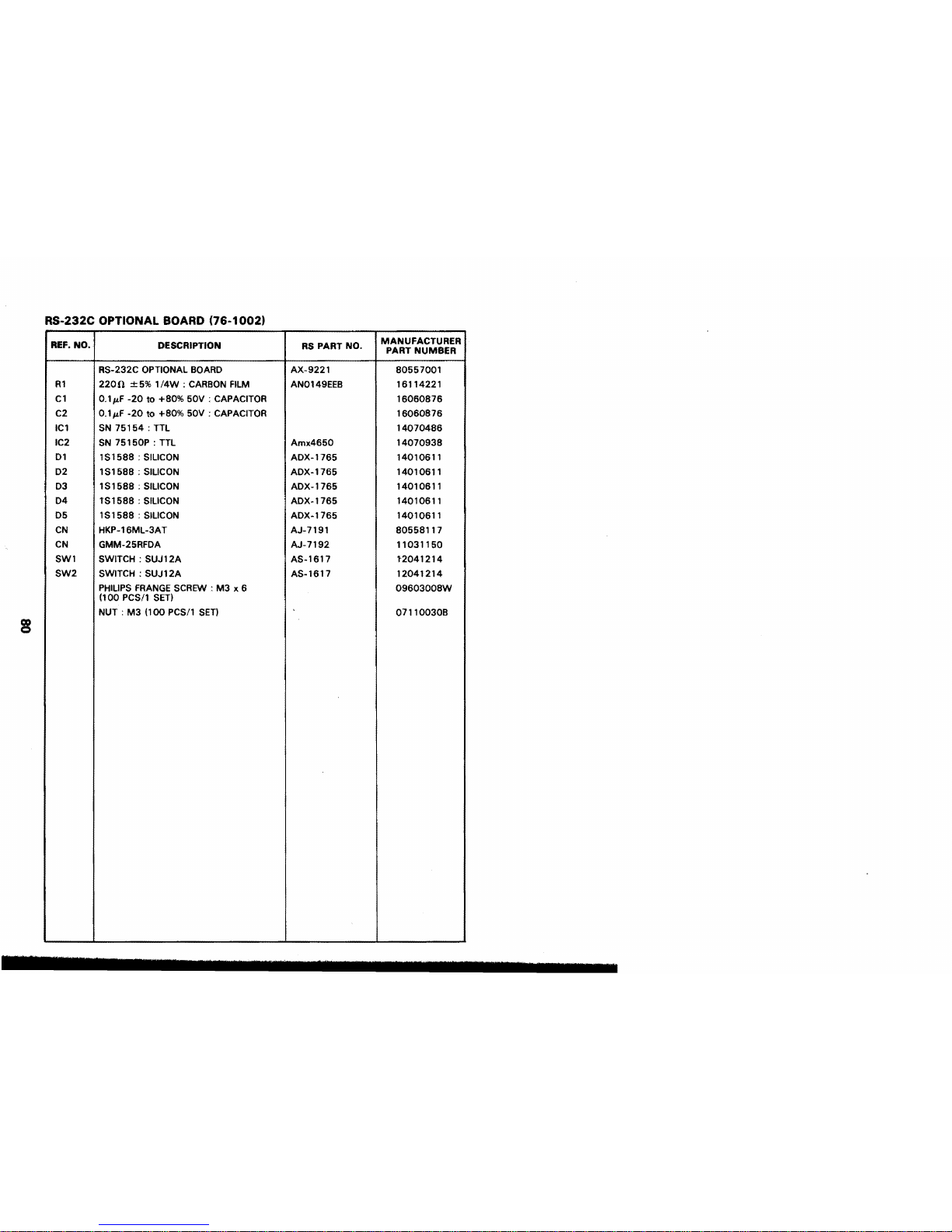
RS-232C OPTIONAL BOARD
(76-1
002)
REF.
NO,
R1
C1
C2
IC 1
IC2
D
1
D2
03
D4
D5
CN
CN
SW1
SW2
DESCRIPTION
US-232C OPTIONAL BOARD
2200
2
5% 114W : CARBON FILM
S.lp,F -20
to
+80% 50V : CAPACITOR
3.1uF -20
to
+80% 50V : CAPACITOR
SN 75154: TTL
SN 751 SOP
:
TTL
IS1588
:
SILICON
IS1588
:
SILICON
IS1 588
:
SILICON
TS1588
:
SILICON
IS1 588
:
SILICON
dKP-16ML-3AT
GMM-25RFDA
SWITCH
:
SUJ12A
SWITCH
:
SUJ12A
PHILIPS FRANCE SCREW
:
M3 x 6
(1 00 PCSII SET)
WJ
:
M3 (100 PCS11 SET)
RS
PART NO.
AX-9221
AN0149EEB
Amx4650
ADX-1765
ADX-1765
ADX- 1765
ADX-1765
ADX-1765
AJ-7191
AJ-7 192
AS-1617
AS-1617
MANUFACTURER
PART NUMBER

MECHANICAL
PARTS
LIST
COVER
UNIT
-
REF.
NO.
DESCRIPTION
UPPER COVER UNIT
UPPER COVER ASSEMBLY
REAR COVER
OPTION COVER (DUST PLATE)
UPPER COVER
FRONT COVER ASSEMBLY
FRONT COVER
MOUTH ASSEMBLY
(NON-REPAIRABLE ASS'Y)
EAR ASSEMBLY
(NON-REPAIRABLE ASS'Y)
INNER COVER
BASE COVER UNIT
BOTTOM COVER
RETAINING PLATE
RUBBER FOOT
AC CAP
FAN ASSEMBLY
FAN MOTOR
PROPERA FAN
FAN BRACKET (FAN ANGLE)
HANDLE
RUBBER BUSH
VARIABLE RESISTOR (VOLUME)
COLOR
:
FAN MOTOR
RUBBER WASHER
:
FAN MOTOR
SCREW
:
M3
x
8
(100 PCSII SET)
SCREW
:
M4 x 16 (100 PCSII SET)
SCREW
:
M3
x
8
(100 PCS11 SET)
HEXAGON HEADLESS SCREW
:
M3
x
6
(100
PCSII SET)
SCREW
:
M3
x
8
(100
PCS11 SET)
PHILIPS SCREW WITH WASHER
:
M3 x 10 (100 PCS/l SET!
RS PART NO.
1
MANUFACTUREF
PART NUMBER

PRINTER UNIT
1EF. NO.
DESCRIPTION
PRINTER UNIT
:
PT-210
LOWER GUIDE
HOLDER SHAFT
PAPER CUTTER ASSEMBLY
PAPER LOCK SPRING
LF MOTOR ASSEMBLY
BELT
:
LF MOTOR TIMING
MOTOR TIMING ASSEMBLY
MOTOR
SHAFT
CR PULLEY
CR TIMING PULLEY
TENSION SPRING LEVER
TENSION SPRING
HEAD LEVER
SOLENOID ASSEMBLY
(NON-REPAIRABLE ASS'Y)
PLATEN SUPPORT
PLATEN
FRAME ASS'Y
:
PT-2 1 0
CABLE ASSEMBLY
(PHOTO INTERRUPT ASS'Y)
TENSION ROLLER
SHAFT
:
TENSION ROLLER
DANCING PIPE
DANCING PIN
PRINTER FRAME
HEAD
:
SHAFT SUPPORT
CR MOTOR ASSEMBLY
MOTOR TIMING PULLEY
HEAD ASS'Y
:
PT-210
HEAD
:
SHAFT
BELT
:
CR TIMING
HEAD SPRING
POSITION PLATE
UNDER HEAD ASSEMBLY
(NON-REPAIRABLE ASS'Y)
THERMAL HEAD ASS'Y
(NON-REPAIRABLE ASS'Y)
TENSION PLATE
FG CABLE
:
LF-SOLENOID-CR
RS PART NO.
Axx5036
AHC1751
AHC1752
ART4373
ARB7602
Am4695
AB6566
ARA0455
AHC1750
ARA0456
AHC1746
ARB7603
AHC 1745
AS9183
AHC 1 748
ART4375
AZ67 19
ART4372
AHC 1749
AH4496
ART4376
AB6565
AHC1743
MANUFACTURER
PART NUMBER
REF. NO,
DESCRIPTION
FG CABLE
:
LF-CR
FG CABLE
:
CR-PSU
HEAD GUIDE
PRINTER LOCK
SCREW M3 x 10
(1
00
PCS11 SET)
SCREW M3 x 5 (1
00
PCS11 SET)
RETAINING RING
:
2MM (100 PCS11 SET)
SCREW
:
M2.5 x 4 (100 PCS11 SET)
SPRING PIN
:
2 x 8 (100 PCS11 SET)
RETAINING RING
:
5MM (100 PCS11 SET)
NUT
:
M4 (100 PCS11 SET)
SCREW
:
M3 x 8 (100 PCS11 SET)
SCREW
:
M3 x 6 (100 PCS11 SET)
WASHER
:
3MM (100 PCS11 SET)
WAVE WASHER
SCREW
:
M4 x 8 (1 00 PCSI1 SET)
RS PART NO.
MANUFACTURER
PART NUMBER

KEYBOARD
UNIT
REF. NO. DESCRIPTION
KEY BOARD UNIT
KEY TOP
:
SPACE
KEY TOP
:
SHIFT
KEY TOP
:
SHIFT
KEY TOP
:
RETURN
KEY TOP
:
CTRL
KEY TOP
:
BREAK
KEY TOP
:
RUB
OUT
KEY TOP
:
ESC
KEY TOP
:
LINE FEED
KEY TOP
:
PAPER ADV
KEY TOP
:
BACK SPACE
KEY TOP
:
REPT
RS PART NO,
MANUFACTURER
PART NUMBER
860037 13
8621 5900
8621 5901
8621 5901
8621 5902
8621 5903
8621 5904
8621 5905
8621 5906
8621 5907
8621 5908
8621 5909
86215910
1 2 1
KEY TOP : !,
I
1
86215911
1
1
2
1
KEY TOP
:
3
I
86215912
I
2
KEY TOP
.'$
2
KEY TOP
:
$
1 2 1
KEY TOP
:
$
8621 591 5
I
1 2 1
KEY TOP
:
1
86215916
1
1
2
1
KEY TOP
:
<fi
1 1
86215917
1
KEY TOP
:
Q
KEY TOP : W
KEY TOP
:
E
KEY TOP
:
R
KEY TOP
:
T
KEY TOP
:
Y
KEY TOP
:
A
KEY TOP : S
KEY TOP
:
D
KEY TOP
:
F
KEY TOP : H
REF. NO,
DESCRIPTION
1
RS PART NO.
KEY TOP
1
+
KEY TOP : Z
KEY TOP
:
X
KEY TOP : C
KEY TOP
:
V
KEY TOP
:
8
KEY TOP
:
KEY TOP : +7c
KEY TOP
:
-8'
KEY TOP : 'g
KEY TOP
:
9&
8
I
KEY TOP:
7
{
KEY TOP
:
KEY TOP
:
6>
MANUFACTURER
PART NUMBER
8621 5932
8621 5933
8621 5934
8621 5935
8621 5936
86215937
'1
1 2 1
KEY TOP:
3>
1
86215947
1
KEY TOP : 2>
1
I
KEY TOP:
,,,,
KEY TOP
:
A
KEY TOP
:
KEY TOP
:
5K'
SLIDE SWITCH
SLIDE SWITCH
SLIDE SWITCH
SLIDE SWITCH
DIODE
:
GREEN
DIODE
:
RED


10/
Exploded
Views


1
I/
Schematic Diagrams
wow

PHOTO
SUPPLY

14LSOZ
P
73
Pie
Vet
vcc
8
Pa
7,-
PROS
PW
23
CPU
7
8039
'Dl
Ill

CONTROL LOGIC
2/2
c

MIC
1H
201
0
2BZ2.7
SP
OUT

MODEM
LOGIC
2/2

POWER
SUPPLY LOGIC
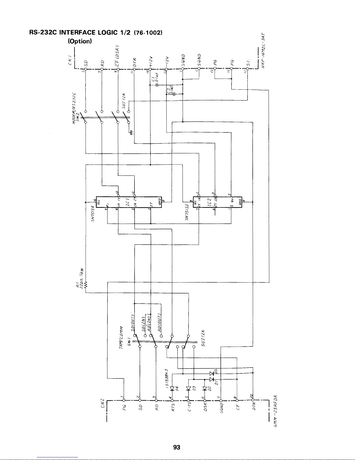
RS-232C INTERFACE LOGIC 1 /2
(76-
1
002)
(Option)

RS-232C INTERFACE LOGIC 2/2
(Option)
(76-1
002)

RADIO SHACK A DIVISION OF TANDY CORPORATION
U.S.A. FORT WORTH. TEXAS
76102
CANADA: BARRIE. ONTARIO
L4M
4W5
TANDY CORPORATION
AUSTRALIA BELGIUM U.
K.
280316 VICTORIA ROAO PARC INDUSTRIEL DE NANINNE BILSTON ROAD WEONESBURY
RYDALMERE N.S.W. 2116 5140 NANINNE WEST MIDLANDS WS10 7JN
Printed
in
Japan
 Loading...