

•
®
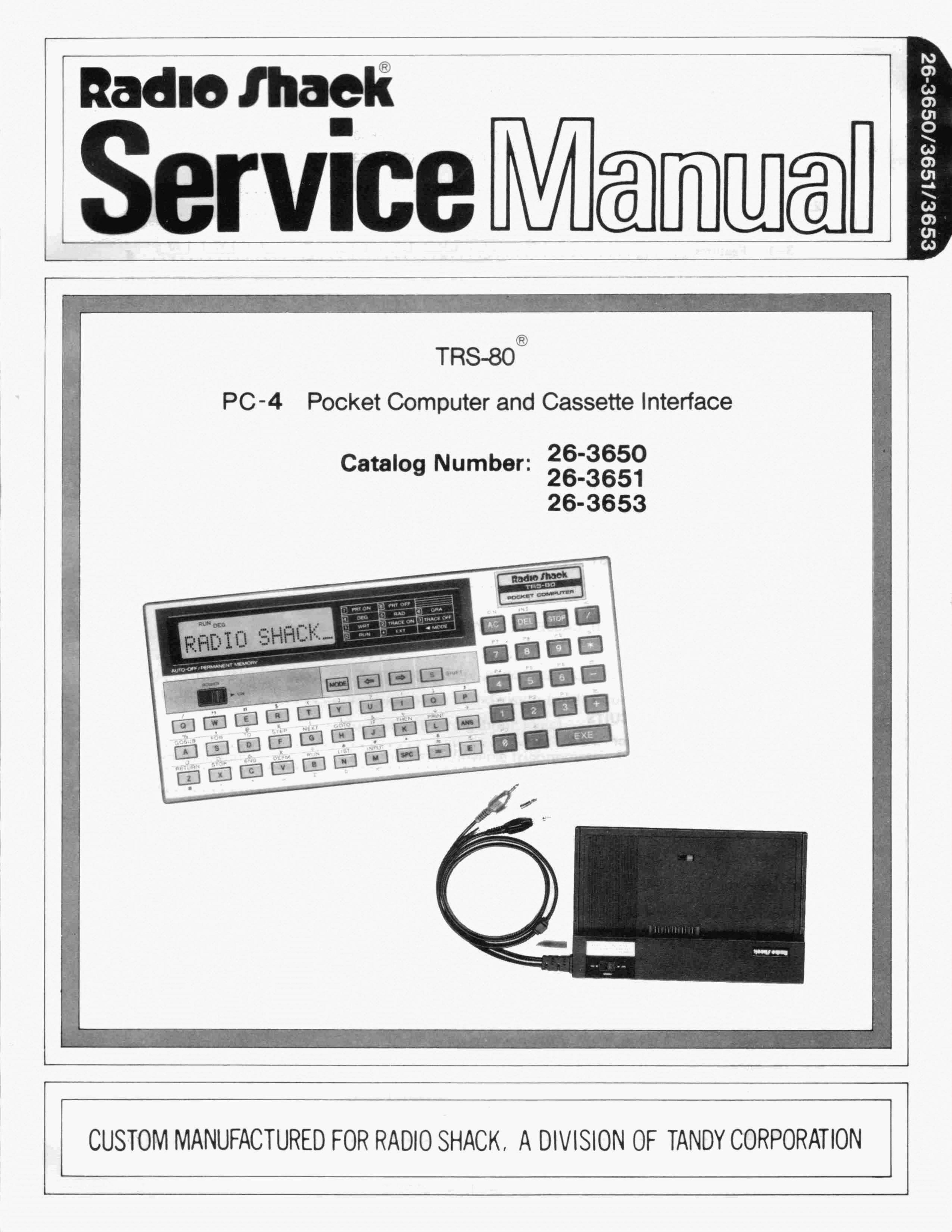
PC-4
TRS-80
Pocket Computer
Catalog Number:
®
and
Cassette Interface
26-3650
26-3651
26-3653
CUSTOM
MANUFACTURED
FOR
RADIO
SHACK,
A
DIVISION
OF
TANDY
CORPORATION

1.
SPECIFfCATlONS
Keyboard
./ .. # $ ( ) ? : ; ,
layout
~~qJCPqJqJ~CP~q;J
GOSUB FOA TO
o
006
Display
IT]
[[]
STEP
NEXT
m [[]
X
..;-
~
L!:!J
~
IF
[1]
..
THEN PRINT
m
IT]
• •
IACI
CD[TI00
000G
~Nsl
[DITJQ]0
[Q] D I
ON
INS <
~
~
P7
P8
P4 P5 P6
P1
P2
PO
t
P9
P3
[ZJ
y
~
L
EXE
.fbisp•
Fundamental calculation
functions:
Built-in functions:
Commands:
Display
Display
.,
tube:
method:
capacity:
AC-61255
5 X 7
11
dot
matrixIiquid
columns
Negative numbers, exponentials, parenthetical addition, subtraction,
multiplication and division
function
Trigonometric/inverse trigonometric functions (angular units-degree/
radian/gradient), logarithmic/exponential functions, square
powers, conversiontointeger, deletionofinteger
value, symbolization, designation
designation
INPUT, PRINT, GOTO, FOR·NEXT, IF-THEN,
STOP,
CLEAR A, DEFM, SAVE, SAVE A, LOAD, LOAD A, PUT, GET,
VER
(alphanumeric
(true algebraic logic)
of
numberofdecimal positions, random numbers, 1f
END, RUN, LIST, LIST A, MODE, SET, VAC, CLEAR,
crystal
characters and symbols)
(with
priority
of
sequence judgement
numberofeffective positions,
portion,
GOSUB,
root,
absolute
RETURN,
Program functions:
Calculation range:
Program system:
KEYiCSR,LEN,MID,VAL
±1
X
10-99
to
±9.999999999 X 10
(internal calculation
Stored system
-1-
uses12mantissa positions)
99
and 0

Program language:
of
Number
steps:
BASIC
Maximum
is
loaded)
544
steps (maximum 1,568 steps when optional
RAM
pack
Program capacity:
Number
Number
of
memories:
of
stacks:
Power supply:
Power consumption:
Battery life:
Auto power
-off:
Dimensions:
Weight:
Maximum
Standard 26, expandable
RAM
10
programs
(PO
through
to
94 (maximum
packisloaded) and exclusive character variable ($)
Subroutine - 8 levels
FOR-NEXT loop - 4 levels
Numerical value - 6 levels
Calculation elements -
Two
lithium batteries (CR2032)
12
levels
Maximum 0.02W
Main frame only -
is
Power
last operation.
9.8mmH
turned
X 165mmWX
approxima1e1y 360 hours (continuous use)
off
automaticallyepproximately 1 minutes after
11mmO
116g (4.1 oz) including batteries
P9)
222
memories when optional
(318"H X 6-112"W X
2·3/4"0)
-2-

2. BLOCK DIAGRAM
HD61913A01
~>
CPU
R1
- R15
-
AC61225
A
"'T
CE1
CE2
LCD
01-08
,--,/
..
~
RAM1
HD61914
~
Ilop
~
K1-
K12
"
KEYBOARD
LCD:
CPU:
RAM:..Stores data and program. Each
12-digit
dot-matrix
display. A characterora numberisdisplayed
5 X 7 dots.
CMOS
VLSI one-chip microprocessor unit.
and contains self-control circuit.
r-----
I
~
.,-
I
I
I"
I
L !
EXPANSION RAM MODULE
RAM
has 1K bytes (8K bits) capacity
RAM2
HD61914
1-----
-,
I
I
I
I
I
I
I
in
- 3 -

3.
CPU
(Central
Processing
Unit) HD61913
3-1.
3-2.
Features
o
CMOS
one-chip
CPU
o Built-in ROM: 100864 bits
o Built-in RAM: 1896 bits
o Built-in display driver
o Memory backup function
o Clock: 400 kHz
Internal machine cycle: 200 kHz
Minimum instruction execute time:
CPU
Block Diagram
ROM
(System
Program)
>-
)
Control signals
11
Instruction
Decoder
lOpS
-"-
-v""
00
~
-.
<
CD
~
_.
III
'tl
-
Ql
-<
Address
Control
/
·vl,
Keyboard
Control
.(
~
I,
~
Keyboard Signals
RAM/ROM
r
Internal Bus
?
•
"\./
ALU
----"..
..
aI
i
./
(')
0
:;,
...
0
2-
- 4 -

3-3.
CPU
Signal Descriptions
Pin No.
1-4
S
6-
18
19
20-
25,
26
27
- 72
73
24
Signal Name In/Out Function
01-
08
INT Not used.
KI2
- Kl
SW
VS-
Vl
050,
R1S
GND
051
-
R7
In/Out
In/Out
In
In
In/Out
Out
In
Data bus. Also designates
signal
OPisHIGH.
input/output
Key
Power switch input signal.
LCD
drive voltages. These voltages are
generated by connecting external resistors
VDD2.
By
connecting
between these terminals, clock pulse
nally generated.
LCD
display signals.
signals.
56
kohm external resistance
o(zero) volt power source.
RAM
address while
is
to
inter-
74,
76
77
78,
80
75
79
CE1, CE2
VDDl
VDD2
4>1,
4>2
OP
Out
In
Out
Out
Out
Chip enable signals. CEl selects
HIGH
HIGH level.
-5.5V
-5.SV
Stays
power-off)
Clock pulses.
When
address bus for
command code
interface.
level
while CE2 designates
input.
output
-S.5Vatpower ON. GoestoOV
the
from
the
LSI.
or
APO (Auto Power-Off).
signalisHIGH,the
RAMs
and also becomes
for
the
optional cassette tape
data bus becomes
RAM1at
RAM2at
at
the
- 5 -

4.
RAM
(Random
Access
Memory)
HD61914is1K byte
The following shows a memory map
t------------------i
RAM 1
t------------------i
RAM
and contains self-control circuits.
System
User's
Memory
Area
of
RAM
1
and
RAM
2 (optional
000
21F
220
7FF
800
RAM
pack).
RAM2
I--.-------------~
Note: The above 8ddr
User's
....
Area
for
C8I8I
when one word
FF F
is
4 bits.
-6-

5. SERVICING
5-1.
Disassembly
- 7 -
1. Remove two screws from the back.
2.
Lift
and slide down
3. Remove the battery cover.
4. Extract batteries.
5. Remove eight screws from
6. Remove the guide plate.
the
lower case.
the
guide plate.

5-2. Trouble shooting
Note: Numbers in CAUSE column
A.
Display
to
LSI's
OPERATION
Turn
the
the
Push
button
computer.
on
function:
power switch on.
ALL RESET
the
backofthe
CPU,
denote
RAM
1
I_RUN_
Dot display
No
DEG
displayatallorunusual indication.
orderofpossibility.
TROUBLE
__
cannot
be shown.
RUN
. "
:
....
!
e"
Some
: :
t :
dots
..
•••
1:
it
cannot
DEG
'" .,
~
't'
•••
• :
.
..
:
....
i:'!
i·
...·
be displayed.
CAUSE
1.
RAM
1
2. CPU
I
CPU
1. CPU
LCD
.
2.
3. Heat
seal
B.
Key Entry
LSI's
to
function:
CPU
RAM
1 Storing entered numbersorcharacters.
TROUBLE
No
entryatall. t.
Cursor moves,
cannot
Only characters can be
be displayed.
but
entered
entered
Key
input
operation, Displaying.
numberorcharacter
CAUSE
CPU
Wiring between
2.
RAM
1.
2.
3.
1.
2.
1
CPU
Wiring between CPU and
CPU
Wiring between
CPU
and keyboard.
CPU
and keyboard.
RAM
1.
- 8 -
C.
RAM 1
(1) Remove optional RAM module
(2)
Push
the
ALL
RESET button on the bottom.
(3) Operate DEFM
(4) Write the following program.
62!EXEI.
if
equipped.
10 FOR I
20 A
(I)
= I
30 PRINT A
40
NEXT
50 PRINT
60 END
(5)
After
writing the above program, confirm that the remaining program step
(6) Execute the program
OK
by every depressionofthe
If
the
above
D.
RAM2
(1) Install the RAM module
(2)
Push
(3) Operate
If
the
operations cannotbemade,
(Optional RAM module)
the
ALL
IMODE] 1
display shows the remaining stepas544
(a)
(b) Wiring between
and
RESET button on the bottom.
and
RAM2isnot
= 1 TO 87
(I)
I
"RAM
confirm
OK"
confirm the display counts up from 1to87
[t~]key.
RAM 1 may be faulty.
in
a PC-4.
that
the remaining program stepis1568.
.
functioning.
CPU
and
RAM2
has
failed.
is
and
shows RAM
O.
(4) Operate. DEFM 190 IEXEI
(5) Write the following program.
10 FOR I
20 A
30 PRINT A
40
NEXT
50 PRINT
(6) Execute the program
MODULE
If
the above programisnot
OKbyevery depression of!EXElkey.
= 1 TO 215
(I)
= I
(I)
I
"MODULE
and
confirm the display counts up
performed, the
and
confirm the display
OK"
RAM2
- 9 -
***VAR:216.
from1to
(optional RAM module) may
215
and
shows
be
at.
fault.
E.
Discrimination Between
If
atest
unit
passes
the preceding checking procedures
follow
(1) Manual Calculations Below
If
(2) Program
the calculations.
Perform the following calculations manually.
1
+ 2)1:
Correct answer
(In
DEG
(TAN(COS(SIN(LOG
Correct
the
above
Execute the following program after pushing the
calculations cannot be
10
FOR
FOR
20 NEXT L : NEXT K : NEXT
30
GOSUB
40
GOSUB
50
GOSUB
60
GOSUB
70
GOSUB
80
GOSUB
90
GOSUB
100 GOSUB 110 RETURN
110 RETURN
CPU
and
(3
+ 4)1:
mode)
answer
made,
I = 1 TO 2 :
L = 1 TO 2
40 PRINT
50 RETURN
60 RETURN
70 RETURN
80 RETURN
90 RETURN
100 RETURN
RAM 1
(5
+ 6)1:
767.
100)
0.0174550616
the
FOR
(7
)))
CPU
may
ALL
J = 1 TO 2 :
J : NEXT
"END"
: END
and
a problem still exists,
+
8)))
IEXEI
be
faulty.
RESET button on the bottom.
K
FOR
After
executionofthis program,
display should show END.
= 1 TO
2:
If
the
above
RAM 1 may
manual calculations (1)
be faulty.
are
done
-10-
but
the program (2) cannot be executed,
 Loading...