

Page 1
AFM2
MODULATION
METER
,
1
Page 2

DIGITALY REMASTERED
OUT OF PRINT- MANUAL SCANS
By
Artek Media
18265 200th St.
Welch, MN 55089
www.artekmedia.com
“High resolution scans of obsolete technical manuals”
If your looking for a quality scanned technical manual in PDF format please visit
our WEB site at
manuals@artekmedia.com and we will be happy to email you a current list of the
manuals we have available.
If you don’t see the manual you need on the list drop us a line anyway we may
still be able to point you to other sources. If you have an existing manual you
would like scanned please write for details. This can often be done very
reasonably in consideration for adding your manual to our library.
Typically the scans in our manuals are done as follows;
1) Typed text pages are typically scanned in black and white at 300 dpi.
2) Photo pages are typically scanned in gray scale mode at 600 dpi
3) Schematic diagram pages are typically scanned in black and white at 600
dpi unless the original manual had colored high lighting (as is the case for
some 70’s vintage Tektronix manuals).
4) Most manuals are text searchable
5) All manuals are fully bookmarked
All data is guaranteed for life (yours or mine … which ever is shorter). If for ANY
REASON your file becomes corrupted, deleted or lost, Artek Media will replace
the file for the price of shipping, or free via FTP download.
Thanks
Dave & Lynn Henderson
Artek Media
www.artekmedia.com or drop us an email at
Page 3
MODULATION
Scans by ArtekMedia © 2008
I
RADIOMETER
COPENHAGEN
n
:
BDE
0
U
Page 4
I
Scans by ArtekMedia © 2008
This
instruction manual
for the type
in mind:
1)
On
page
AM distortion:
Carrier frequencies within
the range
Carrier frequencies within
the range 300
2) Signal-to-noise ratio for each stereo channel measured with a psophometer:
Typically 66 dB at f40 kHz frequency deviation and RF
only when the level of the RF signal
AFM2S6 when the following specification changes and additions are borne
05
read
5
-
300 MHz:
-
1002 MHz:
is
valid for the Modulation Meter, type AFM2, but applies also
for
AFM2S6
0.3% distortion at 30% AM
frequencies, within 20 Hz
1.5% distortion at 90% AM and at modulation
10
frequencies within
1.5% distortion at 30% AM and at modulation
frequencies within 10 Hz
<
200 MHz. These data apply
is
in the 30 - 100 mV range.
Hz - 50 kHz.
cmd
-
1~'kHz.
-.50 kHz.
'
at modulation
Furthermore, it applies to the Modulation Meter, type
06,
07,
D6,
E2,
corrections are made on pages
1
)
AF Output
2) AF Output Terminals
Nominally
when meter reads 3/4 of ful I-scale deflection,
e.g., at *75 kHz deviation in the
deviation range.
3-pol e standard, type
and E4:
AFM2S4S5, when the following
0
dh (0.775
V
rms into 600R)
ZNA
333874/1
f
100
kHz
Page 5
Table
Scans by ArtekMedia © 2008
of
Contents
SECTION A
SECTION
SECTION C
SECTION D
1,
Description
2. Controls, Meters, and Terminals
SECTION
1, Connecting the Instrument
2, Measuring Ampl itude Modulation Percentage
3. Measuring Frequency Deviation
4,
Using a Crystal Oscillator
SECTION F - TECHNICAL DESCRIPTION F 1
-
INTRODUCTION
B - SPECIFICATIONS
-
ACCESSORIES
-
GENERAL DESCRIPTION
E
-
OPERATI NG l NSTRUCTIONS
Plurin
Unit, code 900-252
E
E
E
E3
E4
1
1
1
1,
RF Input Circuit
2, Tuner
3.
IF Filter
IF Preamplifier and IF Attenuator
4,
5, IF Amplifier
P
6,
7,
8.
9,
10, Limiter Stages
11, FM Detector
12, AF Amplifier
13, AF Amplifier Ill
14, AF Detector
1
hase-compensator and Ehnd-pass Filter
Buffer Amplifier
AM Detector
IF Output Amplifier
I
and
I1
-
V
5, Power- Suppl y
SECTION
SECTION H
G
-
-
MA1 NTENANCE
PARTS LIST
Page 6

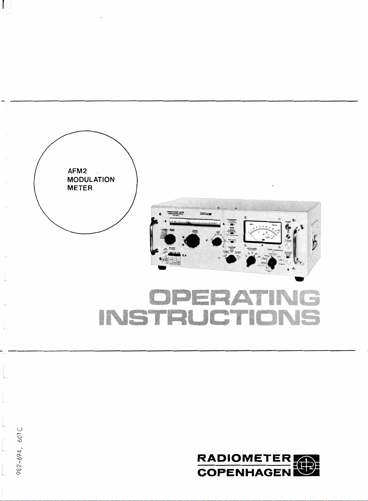
Modulation Meter
Scans by ArtekMedia © 2008
Type AFM2
Section
Fig
.A1
.
The I'tAodulation i'Aeter,
type
AFM2.
The Modulation Meter, type
a solid-state, line- or battery-operated
precision measuring instrument for ac-
curate measurement of the modu
depth of
ation of
quency range from
Modulation Meter
cepting telemetric signals with a modulation frequency up to 200 kHz, and
stereo signals for which it features an
L/R-separation of
The
flection for
and
kti~
srnall amount of residual modulation
generated in the
er, it
and
F"M
measurer( enfs on distol-ted signuls are
AM
signals and the peak devi-
FM
signals in the carrier fre-
5
to 1002 MHz. The
is
designed for ac-
46
dB.
indicating metel- has fuI I -scale de-
3,
76,
30,
53,
*1C,
t
hl\,
is
possible to measure residual
AM
in
signals, and vice versa. Accilrate
k3C1
peak value. Due to the vely
oscillators, sp~~rious
If;GC,
idiodulation Meter plop-
and
AFM2,
lation
1
0C9h
and
AM
is
AM,
zt2C.C
FM
on
A.
Introduction
rendered easy by a
the positive
ue to be measured separately.
creased resolution
nal indicator, such as a voltmeter,
he
ranges downwards.
The input signal level necessury for
occbracy
cy range
range
the range
mcim operating input
Besidzs a manual level control, the
Modulation Meter features
level control with a regulating range
of
To increase the versatility of the Modulation Meter for
row-band equipment, it
two
kHz, just as three standal-d deen~phasis
networks of
non-standard of
four low-pass filters with frequencies of
3,
pass filter with
15
tions for a wide
A
900-252,
swit2l.l that enables
and the negative peak val-
is
desired, an exter-
e--plo)/ed to extend
is
3
mV in the carrier frequen-
5
to
200
2CC
to
60C
SCO
to 1003 MHz. The maxi-
ihe
MHz,
Mtlz, and
20 mV in the
voltage
40
dB.
nreasvren;ants on nar-
is
IF
bandwidths of *20 and k400
50,
75,
and 750
6
dB/octave (ref. 1 kHz),
15,
75, and 200
kHz,
ensure optimal measuring condi-
Crystal Oscillator Unit, code
is
available. See
kHz,
3
dB points at 50 Hz and
range of applicatio~s.
and ore band-
If in-
con
measuring
full
30
mV in
is
10
V.
an
automatic
provided with
s,
one
SECTION
C,
Page 7
Section
Scans by ArtekMedia © 2008
FREQUENCY RANGE OF
INPUT SIGNAL 5
FREQUENCY RANGE OF
VARIABLE
Fundamental ranges: 7-12, 12-21, 21 -37, 37-65, 65-1 10, and
OSCl LLATOR
B.
Specifications
-
1002 MHz
7
-
1000 MHz
11 0-200 MHz
Harmonic ranges:
CALIBRATION ACCURACY 3%
CRYSTAL OPERATION
INPUT LEVEL
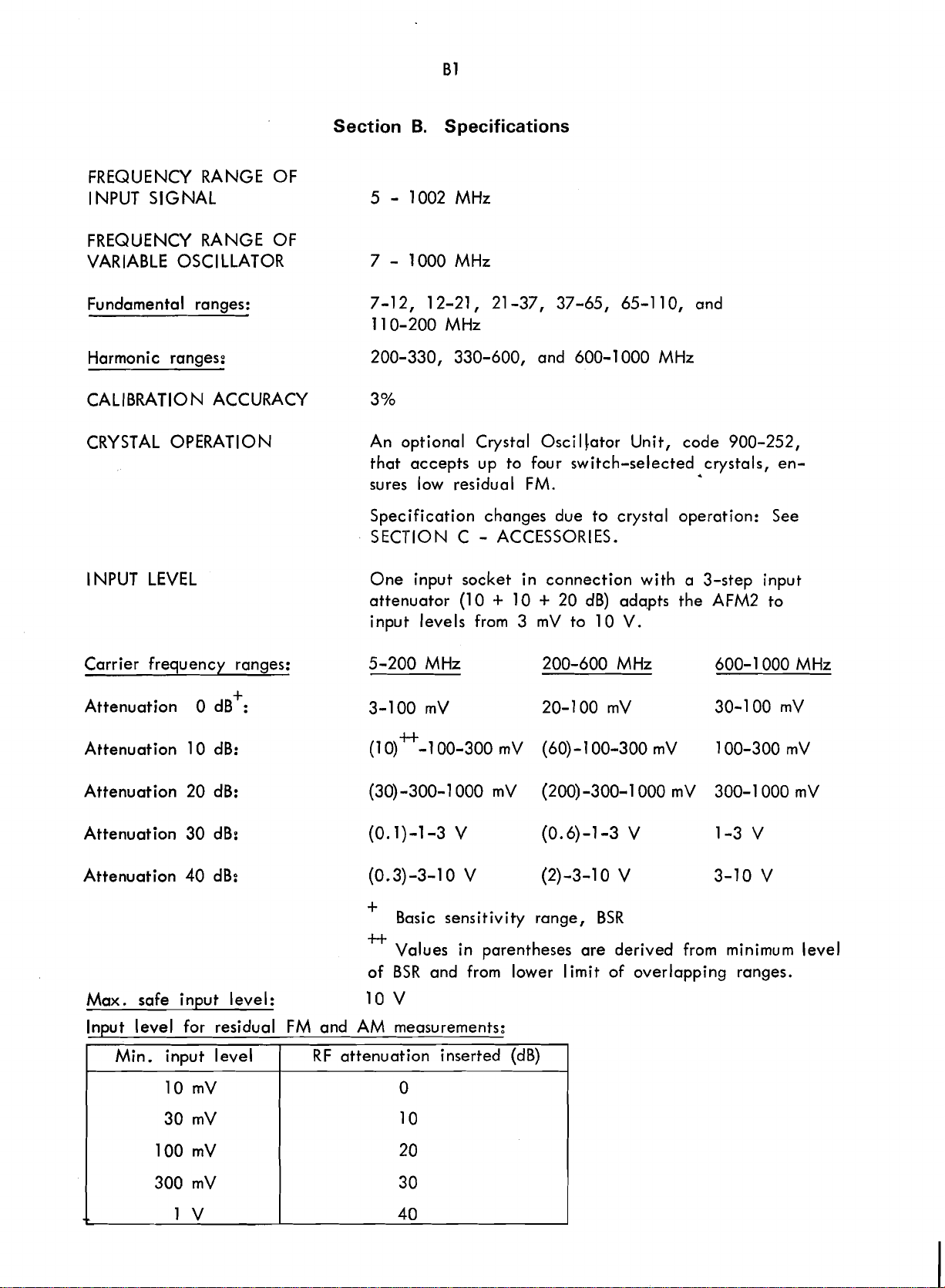
Carrier frequency ranges:
Attenuation 0 dB
Attenuation 10 dB:
Attenuation 20 dB:
+
:
200-330, 330-600, and 600-1 000 MHz
An optional Crystal Osci
that accepts up to four switch-selected crystals, ensures low residual FM.
Specification changes due to crystal operation: See
SECTION C
One input socket in connection with a 3-step input
attenuator (1 0
input levels from
5-200 MHz 200-600 MHz 600-
l lator Unit, code 900-252,
-
ACCESSORIES.
+
10 + 20 dB) ada,pts the AFM2 to
3
mV to 10 V.
1
000 MHz
Attenuation 30
Attenuation 40 dB:
Max.
Input level for residual
I
safe input level: 10 V
Min. input level
dB:
+
Basic sensitivity range,
4-t
Values in parentheses are derived from
BSR
of
FM
and AM measurements:
(
RF attenuation inserted (dB)
and from lower
BSR
limit
of overlapping ranges.
I
minimum
level
Page 8
l
Scans by ArtekMedia © 2008
NPUT IMPEDANCE
50
R
nominal
LEVEL
Manual level setting:
Automatic level setting:
FR
MODULATION
Deviation ranges:
Accuracy:
*75
SETTING
EQ
LI
E
NCY
kHz deviation:
Continuous within a range of min.
The AGC system keeps the level setting within
0.5%
fied input level ranges, inclusive of the overlapping ranges.
Fine adjustment of the automatic level setting
possible
*3,
deviation).
Positive and negative deviation peaks can be mea-
sured separate ly.
2% of reading
quencies within
for input level variations within the speci-
.
*lo,
k30, lt100,
+
1
%
of full scale at modulation fre-
20
Hz - 53 kHz
and
*300
40
dB.
kHz f.s.d.
is
(peak
$300
kHz
deviation:
4%
of reading
quencies within
2% of reading
quencies within
7%
of reading
quencies within
15% of reading
quencies within 125 kHz
Notes:
1.
To obtain specified accuracy, the upper frequency limit of the built-in low-pass filter should be
switched as follows:
Deviation range upper frequency limit
k3
kHz
k10
kHz
*30
kHz 15 kHz
&I00
A300
kHz 75 kHz
kHz
+
1%
of full scale at modulation fre-
10
Hz - 75 kHz.
-t-
1%
of full scale at modulation fre-
20
Hz - 15 kHz.
+
1
%
of full scale at modulation fre-
10
Hz - 125 kHz.
+
1% of full scale at modulation fre-
-
200
kHz.
3
kHz
15
kHz
200
kHz
~andwidths)
(see
2.
The specified accuracies are valid only with the
METER
lower frequency limit
switch set to SLOW.
is
In position FAST, the
160
Hz.
Page 9
Distortion
Scans by ArtekMedia © 2008
k75
kHz deviation:
0.1
10
%
distortion at modulation frequencies within
Hz
-,
15
kHz.
k300
LR-separation of
AF
kHz deviation:
FM
output and meter response
0.2%
20
0.3%
10
0.5%
20
1
10
3%
10
5%
125
stereo signals: For an ideal FM stereo signal (FCC and EBU-stan-
dard), the LR-separation at modulation frequencies
within
distortion at modulation frequencies within
Hz
-
53
kHz.
distortion at modulation frequencies within
Hz
-
75
kHz.
distortion at modulation frequencies within
Hz
-
15
kHz.
.5%
distortion at modulation frequencies within
Hz
-
50
kHz.
distortion at modulation frequencies within
HZ
-
125
kHz.
distortion at modulation frequencies-within
kHz
-
200
kHz.
40
Hz
-
15
kHz
is
greater than
46
dB.
(FM):
AF
output:
Meter response:
Residual
FM:
40
Hz
-
15
Within
than
46
dB (see above). This corresponds to a departure from a linear phase response of less than
and a frequency response within
(40
HZ
-
53
kHz).
Note:
be used.
Within
of the meter
Notes:
1.
used.
2.
METER
the lower frequency limit
On condition of a quiet test room (noise level
<
Less than
range
'The built-in
40
Hz
is
The built-in
The specified response
switch set to SLOW.
60
dB rel.
5-250
2 x 10⁻⁴
25
Hz
MHz; typically
kHz, the LR-separation
+0.25%
200
kHz low-pass filter
-
53
kHz, the frequency response
within
200
FM
+0.25%
kHz low-pass filter
pbar.):
(r.m.s.) within the frequency
and
is
valid only with the
In position FAST,
is
160
Hz.
15
Hz (r.m.s.).
-1.5%.
and
is
is
is
to be
greater
0.5'
-1.5%
to
Less than
typically
100
50
Hz
Hz
FM
(r.m.s.) up to
FM
(r.m.s.).
1002
MHz,
Page 10
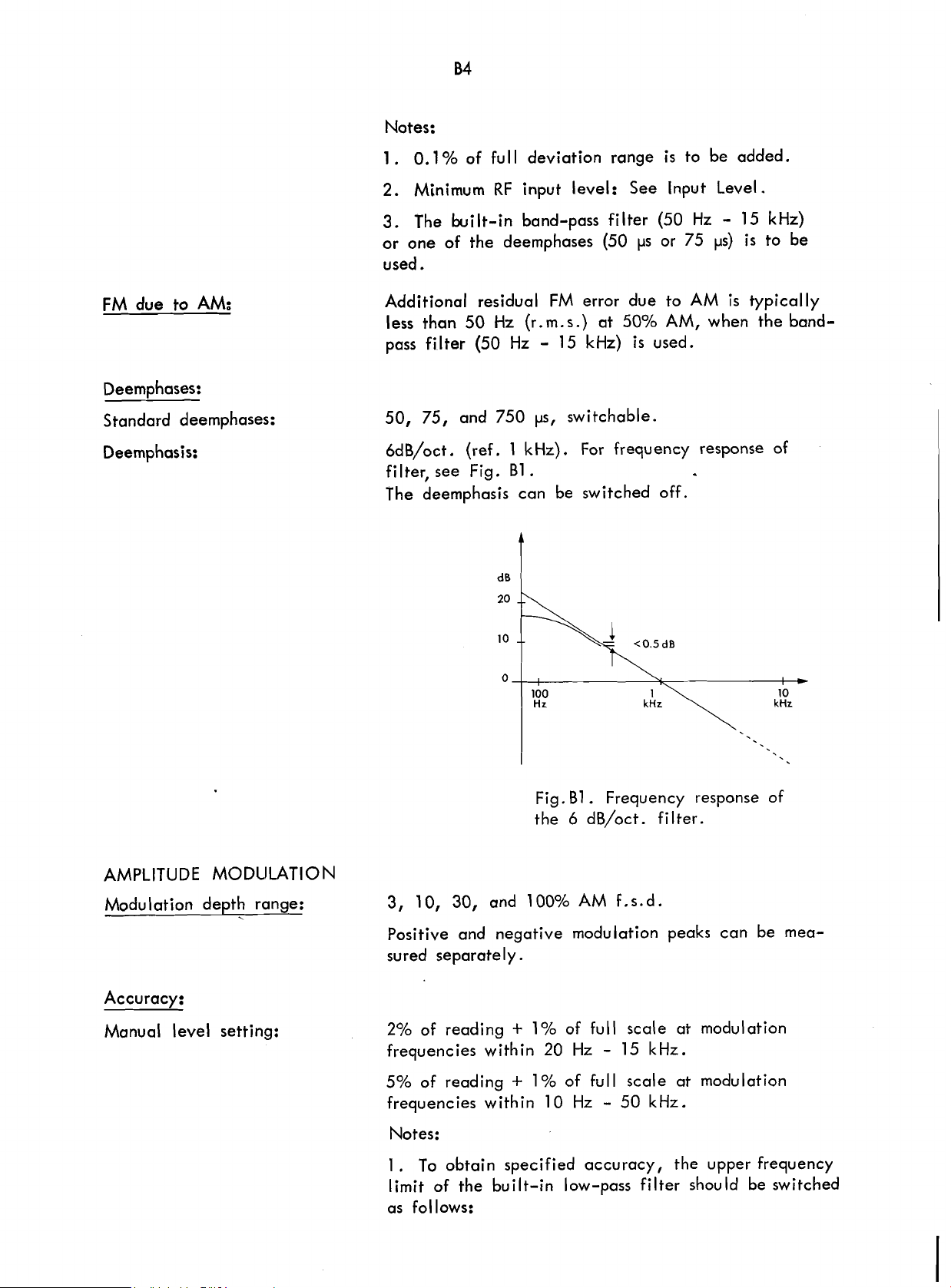
Notes:
Scans by ArtekMedia © 2008
1
.
0.1 % of ful l deviation range
2.
Minimum
3.
the built-in band-pass filter (50 Hz - 15 kHz)
or one of the deemphases (50
used.
RF
input level: See input Level.
is
to be added.
ps or 75
t~s) is
to be
FM
due
to
AM:
Deemphases:
Standard deemphases:
Deemphasis:
Additional residual
less than 50
pass filter (50 Hz
50,
75,
6dB/oct. (ref. 1 kHz). For frequency response of
filter, see Fig.
The deemphasis can be switched off.
Hz
and 750
FM
error due to
(r. m.s.) at 50%
-
15 kHz)
ps,
switchable.
€31
.
is
AM,
used.
AM
is
typically
when the band-
AMPLITUDE
Modulation depth range:
Accuracy:
Manual level setting:
MODLILATION
.
Fig.
€31
.
Frequency response of
6
the
3, 10, 30, and 100%
Positive and negative modulation ~eaks can be mea-
sured separately.
2% of reading
frequencies within 20 Hz
5% of reading
frequencies within 10 Hz
Notes:
1.
To obtain specified accuracy, the upper frequency
limit of the built-in low-pass filter should be switched
as follows:
+
+
1%
1
%
dB/oct. filter.
AM
f.s.d.
of full scale at modulation
-
15
kHz.
of full scale at modulation
-
50
kHz.
Page 11
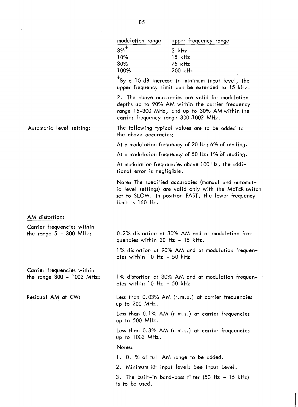
modulation range upper frequency range
Scans by ArtekMedia © 2008
+
3% 3 kHz
10%
30% 75 kHz
1
00% 200 kHz
+
By a 10
upper frequency limit can be extended to 15 kHz.
2. The above accuracies are valid for modulation
depths up to 90% AM within the carrier frequency
range 15-300 MHz, and up to 30% AM within the
carrier frequency range 300-1 002 MHz.
dB
increase in minimum input level, the
15 kHz
Automatic level setting:
AM
distortion:
Carrier frequencies within
the range
5
-
300 MHz:
The following typical values are to be added to
the above accuracies:
At a modulation frequency of 20 Hz:
At a modulation frequency of 50 Hz:
At modulation frequencies above 100 Hz, the addi-
tional error
Note:
ic level settings) are valid only with the
set to SLOW. In position FAST, the lower frequency
limit
0.2% distortion at 30% AM and at modulation
quencies within 20 Hz - 15 kHz.
1%
cies within
The specified accuracies (manual and automat-
is
distortion at 90% AM and at modulation frequen-
is
160 Hz.
10
negligible.
Hz - 50 kHz.
6%
of reading.
1
%
bf
reading.
METER
1
switch
fre-
Carrier frequencies within
the range 300 - 1002 MHz:
Residual
AM
at CW:
1
%
distortion at 30% AM and at modulation frequen-
cies within
Less than 0.03%
up to 200 MHz.
Less than 0.1
up to 500 MHz.
Less than 0.3% AM (r. m.
up to 1002 MHz.
Notes:
1.
0.1% of full AM range to be added.
2. Minimum
3. The built-in band-pass
is
to be used.
10
Hz - 50 kHz
AM
(r.m.s.) at carrier frequencies
%
AM
(r. m.s.) at carrier frequencies
s.)
at carrier frequencies
RF
input level: See Input Level.
filter (50 Hz - 15 kHz)
Page 12
AM due to
Scans by ArtekMedia © 2008
FM:
Additional error
at 550 kHz deviation.
is
less than 0.6% AM (r. m.s.)
AF output
Manual level settings:
Automatic level setting:
l
NTERMEDIATE FREQUENCY CHANNEL
Frequency: 2 MHz
Bandwidths:
IF
check:
IF
outputi
(AM)
'the frequency response
range 20 Hz
The following typical error contributions are to be
added to the above frequency response:
At a modulation frequency of 20 Hz:
At a modulation frequency of 50 Hz:
At modulation frequencies above 100 Hz, the error
contribution
approx.
selected.
The meter has a separate scale to facilitate correct
tuning
2
MHz
correct frequency tuning and full scale deflection on
meter.
is
within 50.5% in the
-
15 kHz.
6%
1
%
is
negligible.
*400 kHz/3 dB and 525 kHz/3 dB, switch-
(IF
=
2 MHz).
IF
signal of 0.2
V
EMF
from 50 Q source at
AUDIO
Bandwidths:
3
kHz filter:
15 kHz filter:
75 kHz filter:
200 kHz filter:
50 Hz - 15 kHz filter:
AF output:
FREQUENCY
CHANNEL
four switchable low-pass filters, 3 kHz, 15 kHz,
75 kHz, and 200 kHz, to be used when measuring
FM
deviation and AM modulation.
for mod. freq. up to
for mod. freq. up to 15 kHz.
for mod. freq. up to 75 kHz and for measurements
of
FM
stereo deviation.
for mod. freq. up to 200 kHz and for measurements
of stereo
(bandwidth: 10 Hz (0.1 dB)
Band-pass filter, 50 Hz (3 dB)
to be used when measuring residual
AF signal of
deflection.
Bandwidth as specified above.
ac- or dc-coupl ing.
L/R
1
separation.
V
3
kHz
-
350 kHz (3 dB)
-
15 kHz (3 dB),
FM
EMF
(peak value) at full scale
A
switch provides for
)
and AM.
ac-coupl ing: Output impedance: 600
pF.
10
dc-coupl ing: Output impedance; 600
Q
in series with
Q.
Page 13
dc OLITPUTS
Scans by ArtekMedia © 2008
IF
level:
1
V
EMF
dc-voltage of
deflection to set level mark.
from 600 R source at meter
IF
frequency:
Modulation:
POWER
Power line:
VoI tages:
Frequencies:
Consumption:
External dc
dc sources:
Current drain:
TERM1
SUPPLY
NALS
supply:
dc-voltage of
deflection to
dc-voltage of
scale deflection.
110
V
and 220
48 - 65
about 25
The power cord
plug of the Schuko type.
0
to
approx.
HZ.
+(I8
400
1
V EMF from 600 R source at meter
IF
CHECK mark (50
1
V
EMF
V,
~10%.
VA.
is
fixed and provided with a mains
to 25
Lq
and 0 to -(I8 to 25
mA from each source.
from 500
mV/100
5:
source at full
kHz).
V)
.
RF
input and
AF output:
dc output
External - dc supply:
Operating ambient temperature
range:
DIMENSIONS AND
Height:
Width:
Depth:
Weight:
MOUNTING
ACCESSORIES
(AF):
AND
IF
output:
FINISH
SUPPLl
WEIGHT
ED
B
NC
UHF
Banana jacks
Bel
l
ing Lee
197
mm
485 mm
245 mm
13
kg (28.6 Ibs)
Steel cabinet finished in grey enamel lacquer.
1
coaxial cable
UG-88/U BNC plugs.
type
(7
3/4
(19
(9
5/8 in.)
1.1
1/8
436;'s
in.)
in.)
(50
O),
code 017-004, with
ACCESSORIES
AVAl LABLE
1
battery plug, Belling
Crystal Oscillator, code 900-252.
1
set of dust covers (top plate and bottom plate)
for rack mounting, code 884-002
&
Lee,
L1436/P,
code 805-429.
Page 14
Section
Scans by ArtekMedia © 2008
C.
Accessories
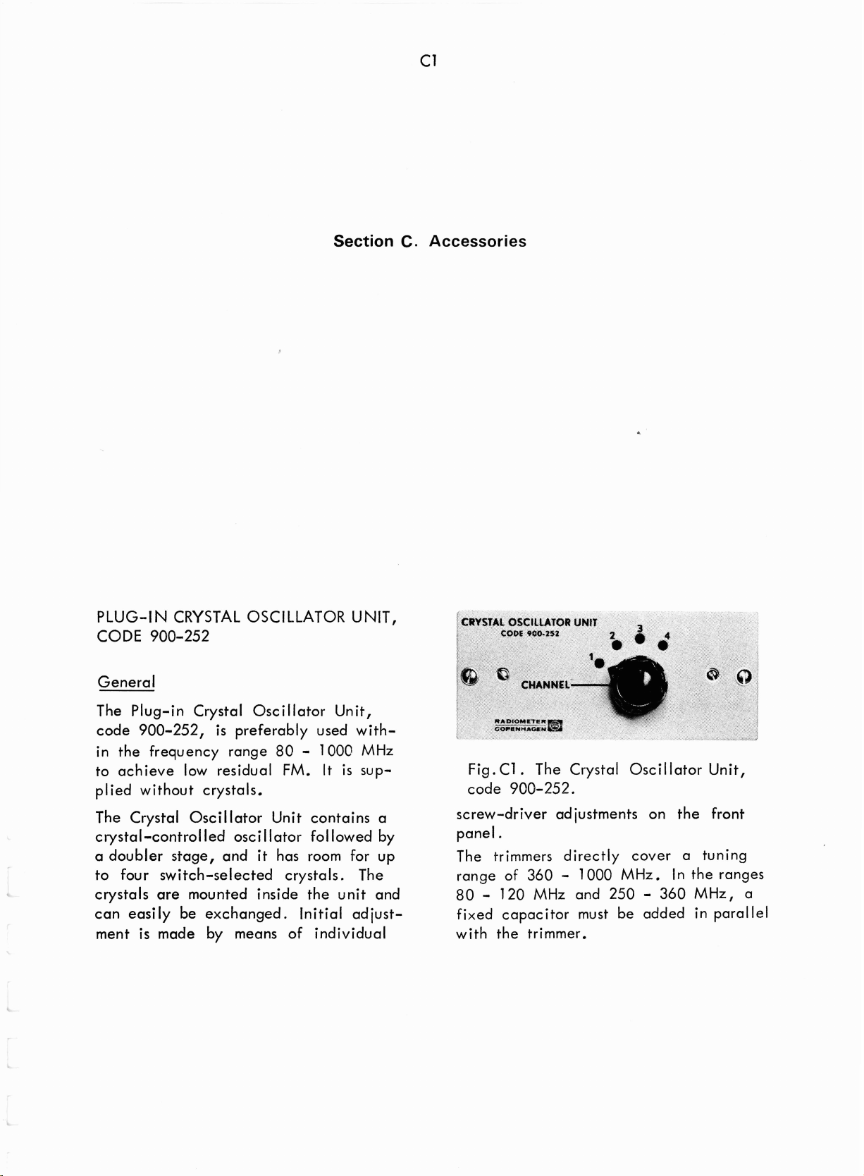
PLUG-IN
CODE 900-252
General
The Plug-in Crystal Oscillator Unit,
code 900-252,
in the frequency range 80
to achieve low residual
plied without crystals.
The Crystal Oscillator Unit contains
crystal-controlled oscillator followed by
a
doubler stage, and
to four switch-selected crystals. The
crystals are mounted inside the unit and
can easily
ment
CRYSTAL
is
be
exchanged. Initial adjust-
is
made by means
OSCILLATOR UNIT,
preferably used with-
-
1000
MHz
FM.
It
is
sup-
a
it
has room for up
of
individual
Fig.
C1.
The Crystal Oscillator Unit,
code
900-252.
screw-driver adjustments on the front
.
panel
The trimmers directly cover a tuning
range of 360
80
-
120
fixed capacitor must be added in parallel
with the trimmer.
MHz
-
1000
and
MHz.
250
In the ranges
-
360
MHz,
a
Page 15
Specifications
Scans by ArtekMedia © 2008
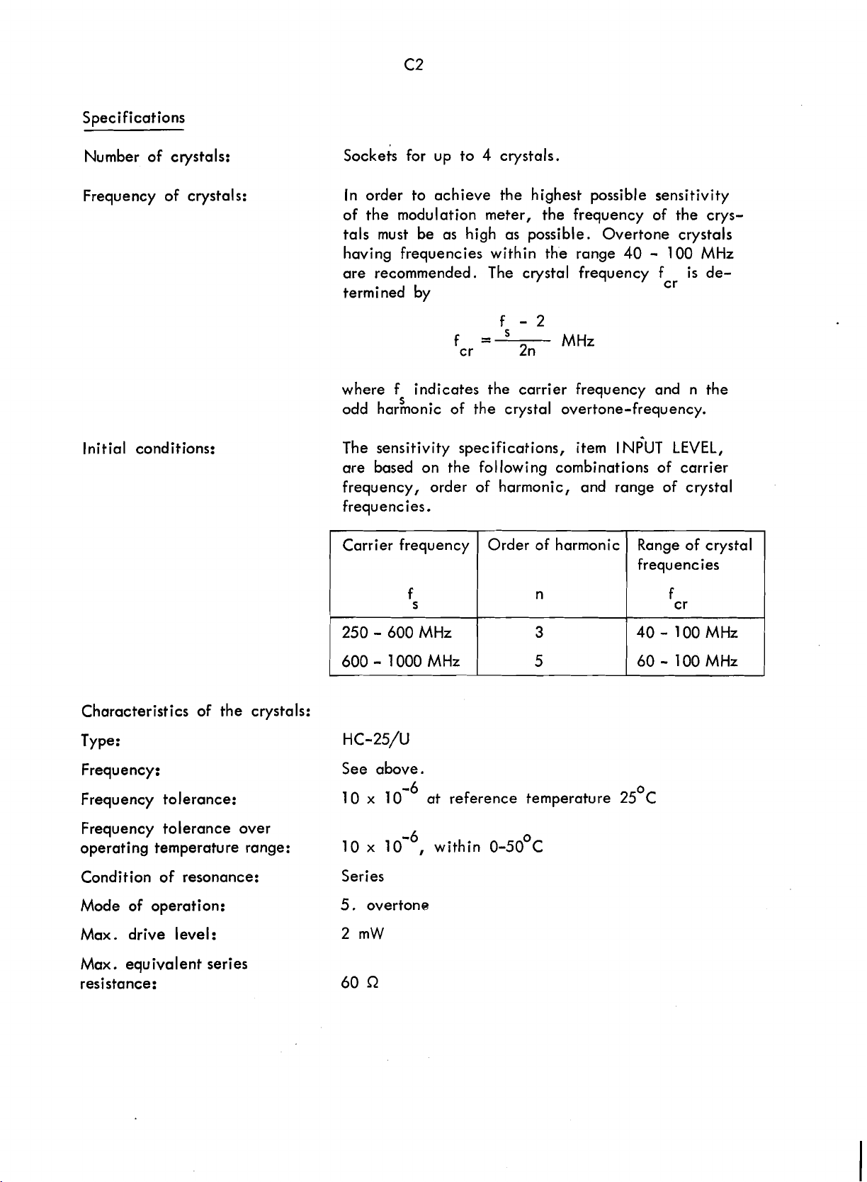
Number of crystals:
sockets for up to
4
crystals.
Frequency of crystals:
lni tial conditions:
In order to achieve the highest possible sensitivity
of the modulation meter, the frequency of the crystals must be as high as possible. Overtone crystals
-
100
having frequencies within the range 40
are recommended. The crystal frequency f
termined by
f -2
f=
cr 2n
where f indicates the carrier frequency and n the
odd harmonic of the crystal overtone-frequency.
The sensitivity specifications, item
are based on the following combinations of carrier
frequency, order of harmonic, and range of crystal
frequencies.
Carrier frequency
s
f
s
s
Order of harmonic
MHz
n
l
NPUT
Range of crystal
frequencies
MHz
is
cr
LEVEL,
f
cr
de-
Characteristics of the crystals:
Type:
Frequency:
Frequency tolerance:
Frequency tolerance over
operating temperature range:
Condition of resonance:
Mode of operation:
Max. drive level:
Max. equivalent series
resistance:
250 - 600 MHz
600 - 1000 MHz
HC-25/U
See above.
10 x
10
x
Series
5.
overtone
2
mW
at reference temperature 25
within 0-50'~
3
5
4060
-
0
C
l00MHz
I00
MHz
Page 16
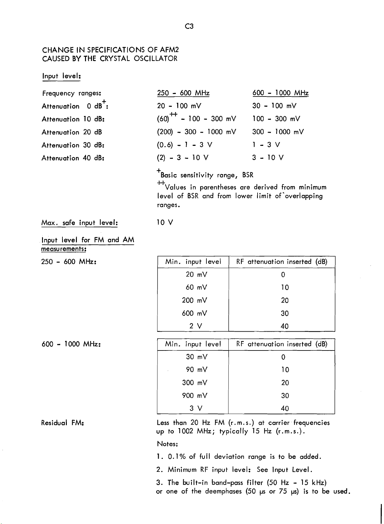
CHANGE
Scans by ArtekMedia © 2008
CAUSED BY THE CRYSTAL OSCILLATOR
lnput level:
Frequency ranges: 250
Attenuation 0 dB
IN
SPECIFICATIONS OF AFM2
+
:
-
20 - 100 mV 30 - 100
600 MHz 600 - 1000 MHz
mV
Attenuation 10 dB:
Attenuation 20 dB
Attenuation 30 dB:
Attenuation 40 dB:
Max. safe
lnput level for FM and AM
measurements:
250
-
in~ut level: 10
600 MHz:
(60)*
(200)
(0.6)
(2)
+
Basic sensitivity range, BSR
u
level of
ranges.
I
-
100 - 300 mV 100 - 300 mV
-
300 - 1000 mV 300 - 1000 mV
- 1 -
- 3 -
Values
V
Min. input level 1 RF attenuation inserted (dB)
3 V 1 -3V
1OV
in
parentheses are derived from minimum
BSR
and from lower
3-10V
limit
of*overlapping
I
600
-
1000 MHz:
Residual FM:
1
Min. input level
Less than 20 Hz FM (r.m.s.) at carrier - frequencies
to
up
1 . 0.1 % of fu
2. Minimum RF input level: See lnput Level.
3. The built-in band-pass filter (50 Hz
or one of the deemphases (50
1002 MHz; typically 15 Hz (r.m.s.).
11
1
RF
attenuation inserted (dB)
deviation range
ps
is
to be added.
-
15 kHz)
or
75 ps)
is
to be used.
(
Page 17
Residudl AM at
Scans by ArtekMedia © 2008
CWo
Less than 0.15% (r.
to 1000
Notes:
1
.
MHz.
0.1 % of full
AM
m.
s.) at carrier frequencies up
range must be added.
2.
Minimum
3.
The built-in band-pass filter (50
is
to be used.
RF
input level:
See Input Level.
Hz
-
15
kHz)
Page 18
Section
Scans by ArtekMedia © 2008
D.
General Description
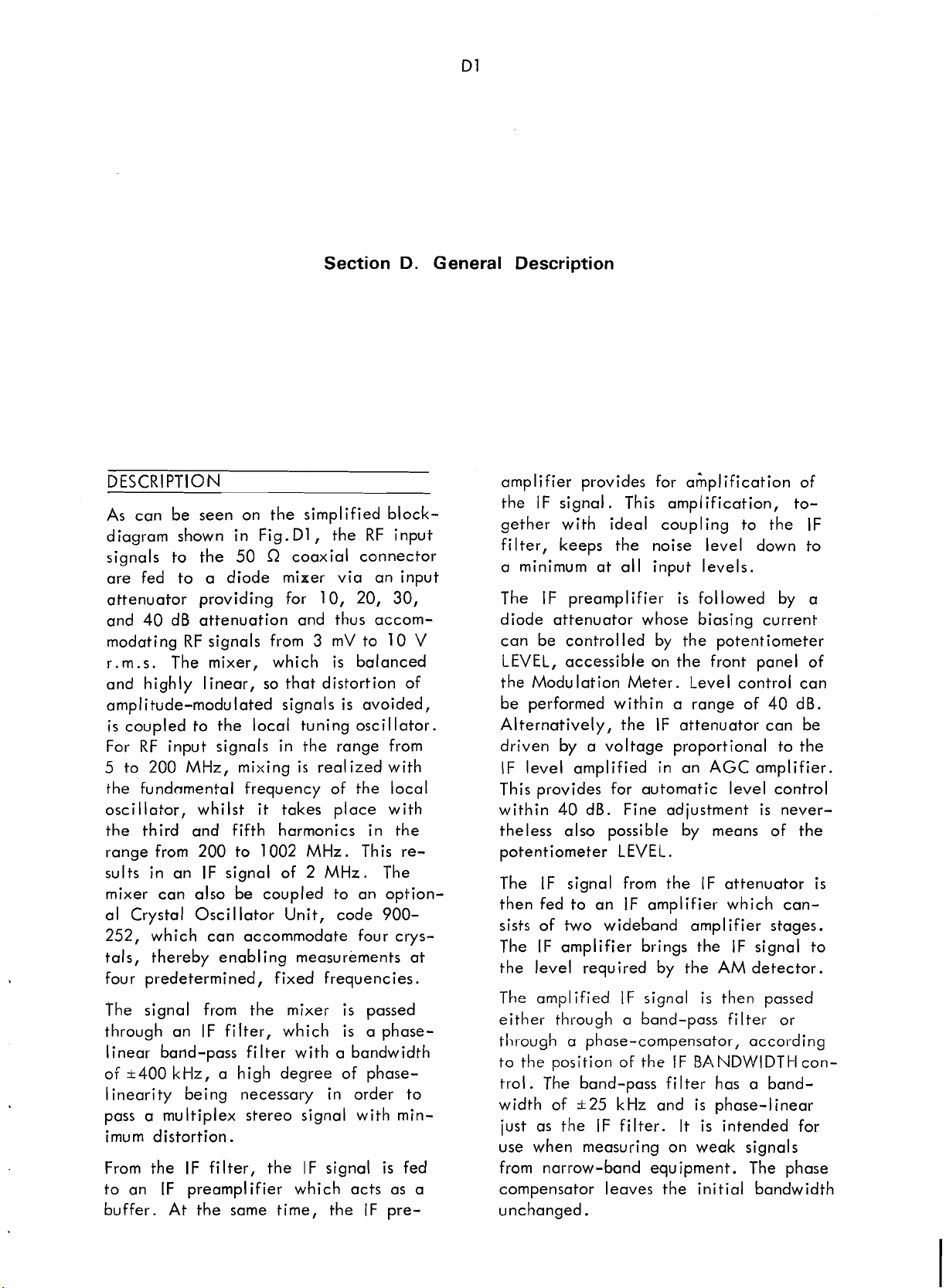
DESCRIPTION
As can be seen on the
diagram shown in
signals to the 50
are fed to a diode mixer via an input
attenuator providing for 10, 20, 30,
and 40 dB attenuation and thus accom-
RF
modating
r.m.s. The mixer, which
highly linear, so that distortion of
and
amplitude-modulated signals
is
coupled to the local tuning oscillator.
RF
For
5 to 200 MHz, mixing
the fundnmental frequency of the local
oscilla:or, whilst it takes place with
the third and fifth harmonics in the
range from 200 to 1002 MHz.
sults in an
mixer can also be coupled to an option-
al Crystal Oscillator Unit,
252, which can accommodate four crystals, thereby enabling measurements at
four predetermined, fixed frequencies.
the signal from the mixer
through an IF filter, which
linear band-pass filter with
of
1400 kHz, a high degree of phase-
linearity being necessary in order to
pass a multiplex stereo signal with min-
imum distortion.
From the
to an
buffer. At the same time, the
IF
signals from 3 mV to 10 V
input signals in the range from
IF
signal of 2 MHz. The
IF
filter, the
preamplifier which acts as a
simplified block-
Fig.
Dl
,
the
Cl
coaxial connector
is
balanced
is
is
realized with
code
is
is
a
bandwidth
IF
signal
RF
input
avoided,
This
re-
900-
passed
a phase-
is
fed
IF
pre-
amplifier provides for
the
IF signal.
gether with ideal coupling to the
filter, keeps the noise level down to
a minimum at all input levels.
The
IF
preamplifier
diode attenuator whose biasing current
can be controlled
LEVEL, accessible on the front panel of
the Modulation Meter. Level control can
be performed within a range of 40 dB.
Alternatively, the
driven by a voltage proportional to the
IF
level amplified in an AGC amplifier.
This
provides for automatic level control
within 40 dB. Fine adjustment
theless also possible by means of the
potentiometer
The
IF
signal from the
then fed to an
sists of two wideband amplifier stages.
The
IF
amplifier brings the
the level required by the
The
amplified
either through
through a phase-compensator, according
to the position of the
.
The band-pass filter has a band-
trol
width of
just as the
use when measuring on weak signals
from narrow-band equipment. The phase
compensator leaves the initial bandwidth
unchanged.
A25
This
LEVEL.
IF
1F
a
kHz and
IF
filter. It
ahplification of
amplification, to-
is
followed
by
the potentiometer
IF
attenuator can be
IF
attenuator
amplifier which can-
AM
signal
band-pass filter or
is
then passed
IF
BANDWIDTH con-
is
phase-linear
is
intended for
is
IF
signal to
detector.
by
never-
IF
a
is
Page 19
A buffer amplifier separates filters, AM
Scans by ArtekMedia © 2008
detector and
sists of a unity-gain amplifier with low
output impedance and serves to suppress
any influence from the
is
available for external monitoring from
a coaxial connector on the front panel.
IF
The
is
fed both to the AM detector and to
the
IF
output amplifier. The AM detec-
tor
is
an amplifier with a mean-value
detector in the feedback loop which
also provides for the large amount of
linearity required. The AM detector has
a
dc and an ac output. The first of
these
strument via the FUNCTION selector.
In the corresponding position of the
FUNCTION selector, the meter indicates the value of the AM detector's
dc current
el. The second output of the AM detector
below) via the selector FUNCTION.
As stated above, the
buffer amplifier
output amplifier which provides for amplification so that the level required for
driving a following limiter
The limiter transforms the
a square wave, the zero crossing of
which
peak-to-peak value being compared with
variations in the mean value. Subsequent
limiting action takes place in the following limiter section. The resulting signal
is
detector section which consists of a
monostable multivi
amplifier.
The signal from the last limiter section
is
vibrator which provides for pulses of
constant width. The
tivibrator are amplified in an output amplifier. The output
with a regulating loop consisting of a
peak detector and an amplifier.
regulating loop keeps the value of the
peak-to-peak voltage of the output am-
is
is
coupled to the AF section (described
is
fed via a buffer amplifier to the
used to trigger a monostable multi-
IF
output amplifier. It con-
IF
output which
signal from the buffer amplifier
coupled to the meter of the in-
-
in other words: the IF lev-
IF
signal from the
is
also fed to the
is
obtained.
IF
signal into
controlled by variations in the
IF
FM
brator and an output
pulses from the mul-
amp1 ifier
is
provided
This
pl ifier constant. Hence, as the amplitude
and the width of the pulses are constant,
the mean value of the signal will vary
according to the number of pulses per
second. The mean value
when the
sition IF CHECK for reading the value
of the intermediate frequency. To ensure
a
high degree of accuracy and an extreme-
ly low hum level, both the multivibrator
and the output amplifier are furnished
with their own regulated power supply.
From the AM or
is
fed to a low-pass filter via a relay
controlled by the FUNCTION selector.
The low-pass filter features the
gree of
ing stereo information without any disturbing influence on
The low-pass filter
two-section,
uator which determines the metering
ranges.
providing for amplification
signal to the level required by the next
stages.
The AF amplifier
phasis networks providing for the stan-
dard deemphases of 50, 75, and 750
and the non-standard deemphasis of
dB/oct. The amplified AF signal can
also be passed through one of four
pass filters with frequencies of
75 and 200 kHz, or through a
pass filter with 3 dB points at 50 Hz
and 15
applications.
These networks and filters are followed
by an AF amplifier.
from this amplifier
front panel via the AF OUTPUT connector for distortion measurements or
external monitoring.
OUTPUT does not interfere with the me-
ter indication. The output voltage from
the first AF amplifier
other AF amplifier providing for the
voltage necessary for the AF detector.
The signal from the AF OUTPUT can
either be dc-coupled or ac-coupled to
FUNCTION selector
FM
detector, the signal
phase-l inearity required for pass-
L/R
is
4
x 10 dB precision atten-
It
is
followed by an amplifier
is
followed
kHz,
ensuring a wide range of
is
is
utilized
is
in po-
high de-
separation.
followed
of
by
by
the
deem-
a
AF
pi,
6
low-
3,
15,
band-
The output signal
available on the
Loading of the AF
is
also fed to an-
Page 20
q-
Scans by ArtekMedia © 2008
-
R
F
Input
XI1
R
F Local
Att.
t
Mixer
-
ROMAN FIGURES REFER TO
DIAGRAM NUMBER
*.N AUTO
TUYlYC
\
osc.
..,,,""""G
/
/
/
111
\
\
\
I
I
Em
/
/
/
/
/
/
/
/
/
"!t!!%!!!H
,,9.".
u
..O~.".
I
v
I
-
11
IF Frequency
"~*.!tEE
4s
I
1
I F
111
IF
Output
1
L
\r
VI
7,
7,
VII
10
2"
\
\
\
Att.
XI1
-
Low
Pass
Filter
\\
Vlll
\
\
'
-
\
\
\
\
_FM+
IF Check
/
"-
/
I..,~.
-8
VIIL
/
/
/
Fig.
Filters
Deem-
phases
/
/
/
/
I
I
I
$.YE!.!
Kl°C
m
Dl
. Block-diagram of
-
-
IF
Level
I
x
olF Check
I
the
\
1.
\
\
,,"El
.SZ.<G.
SLOW
lbl,
WG- ,C".,U
I
l__(.l.l,l.l,e*.
Em
Modulation
Meter,
\
I.
C*ICI
type
\
\
\
Y%"
zi::
AFM2.
IF
CHICI
Level
Page 21
the AF OUTPUT connector by sliding
Scans by ArtekMedia © 2008
the switch.
tions according to the position of the
switch MAN.-AUTO.
The AF detector gives the true peak value of any AF signal. Depending on the
position of the FUNCTION selector, the
positive or the negative modulation peak
can be measured. The AF detector has
two time constants, thereby furnishing
two meter responses.
The AF detector
pedance-matching network providing for
low output impedance to the meter.
CONTROLS,
General
As can be seen in Fig. D2 and
Modulation Meter, type
provided with the following controls,
meter, and terminals:
Controls, Meter, and Front Plate Termin-
als (see Fig. D2)
Power Lamp and
The power switch
monitored
RANGE Selector and Drum Scale (2)
The selector RANGE
tion rotary switch. In the first six po-
sitions, the RANGE selector provides
for selection of the frequency ranges
according to the table printed on the
front plate of the instrument. (Note
that the ranges
frequency bands.) The next position
a rest position. In the last position,
the plug-in Crystal Oscillator Unit (if
any)
is
monitored
ately above.
TUNING Knob (3)
The knob TUNING provides for adjust-
ment of the local oscillator frequency
at
2
is
monitored by a cursor on the drum scale.
LEVEL Potentiometer (4) and MAN.
AUTO. Switch
by
is
connected. The selector
MHz from the signal frequency. It
is
followed
METER,
the lamp POWER.
E
by
AND
ON
switch (1)
OIV
is
is
and F .each cover two
the drum scale immedi-
by
TERMI
D4, the
AFM2,
a toggle switch
an eight-posi-
(5)
an im-
NALS
is
is
RANGE
-
When the switch MAN. -AUTO.
position
ter
instrument manually within a range of
min. 40 dB.
When the switch MAN.-AUTO.
,position AUTO., the LEVEL potentiome-
ter
automatical
i
nstrument.
FUNCTION Selector
The selector FUNCTION
position rotary switch. The position
LEVEL
nal
IF
level. When measuring, the positions
IF
ment to the exact carrier frequency.
(See under "Meter" below) The percentage of amplitude modulation of AM signals can be measured by placing the
selector in position AM
cording to the sign of the modulation
peak to be measured. The frequency
deviation of
sured
FM
the modulation peak to be measured.
METER
'the selector
position rotary switch. Each position
corresponds to the fu
the meter, viz: AM
loo%,
METER
The switch
In position SLOW
meter response
should not be used when measuring on
signals with modulating frequencies
higher than 160 Hz.
mod
fast.
IF
MAN.,
is
used to vary the sensitivity of the
is
used for fine-adjustment of the
ly adjusted sensitivity of the
the LEVEL potentiome-
(6)
is
a
is
used when searcfiing the sig-
(i.e., tuning) and monitoring the
CHECK are used to tune the instru-
+
or AM - ac-
FM
signals can be rhea-
by
placing the selector in position
+
or FM - according to the sign of
RANGE
FM3
Switch
>I60 Hz, the meter response
BANDWIDTH
Selector
METER
-
10
-30
(8)
METER
is
(9)
(7)
RANGE
l
I-scale range of
3
-
10 - 30
-
100
-
is
a sliding switch.
fmod >10 Hz, the
slow. This position
In
position FAST
is
is
seven-
is
a five-
300kHz.
in
in
-
is
The potentiometer LEVEL has two func-
The switch IF BAbIDWIDTH
is
a sliding
Page 22
Fig.D2. Front plate of the Modulation Meter, type AFM2.
Scans by ArtekMedia © 2008
switch. It provides for switching from
the band-pass filter to the phase-comparator and vice versa,
width of k25 kHz to one of k400kHz.
AF
FlLTER/DEEMPHASIS Selector (1 0)
The selector AF
a nine-position rotary switch. In the scales.
first position
a
band-pass filter
used when measuring residual AM and
FM.
kHz
REO),
pass filters are switched in. They are
used when measuring
AM
filters are used for modulation frequencies up to 3 kHz and 15 kHz, respective-
In the next four positions - 200
(L/R
STEREO), 75 kHz
15 kHz, and 3 kHz - four low-
modulation. The 3 kHz and 15 kHz
FI
-
50 Hz- 15 kHz (3 dB)
i
.
e
.,
from a band-
LTER/DEEMPHASIS
is
switched in. It
(A
f,
FM
deviation or
is
-
is
STE-
IY.
is
The 75 kHz filter
tion frequencies up to 75 kHz and for
measurements of
The last filter - 200 kHz
modulation frequencies up to 200 kHz
and for measurements of stereo L/R
separation (bandwidth: 10 Hz (0.1 dB)
-
350 kHz (3 dB)
The last four positions of the AF FILTER/
DEEMPHAS
emphases of 50
IS
selector introduce four de-
p,
used for modula-
FM
stereo deviation.
-
is
).
75p
(European and
used for
American standard for stereo work), 750
ps (narrow-band equipment) and a 6 dB/
oct (non-standard)
Meter
The meter of the Modulation Meter,
type
sion type. It
The upper scale
ing in the AM ranges from
0 to
or
from
viation, according to the positions of
the FUNCTION selector and the
RANGE selector. It
with a LEVEL mark to permit setting of
IF
the
The middle scale (12) provides for read-
ing in the AM ranges from 0 to 3% or
0
to 30%, and in the
0 to 3 kHz, Oto30kHz, or 0 to 300
kHz deviation, according to the position
of the FUNCTION and
I
ec tors.
se
The lower scale (13)
checking the frequency of the converted
signal.
viation around the 2 MHz intermediate
frequency. An
for exact tuning to the intermediate fre-
quency
AFM2,
loo%,
0
to
level.
It
.
.
is
of the taut-band suspen-
is
provided with three
(1
1)
provides for read-
0
to 10%
and in the
10
kHz or 0 to
is
is
graduated for k300 kHz de-
IF
CHECK mark provides
FM
ranges
100
kHz de-
also provided
FM
ranges from
METER
is
utilized when
RANGE
METER
Page 23
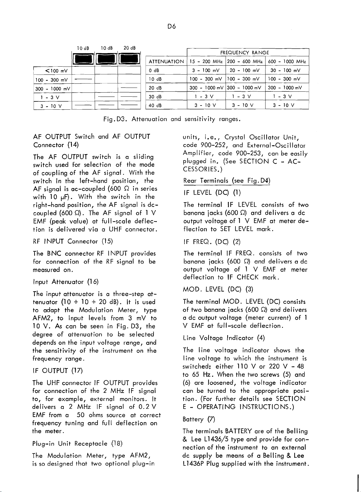
lOdB lOdB 20dB
Scans by ArtekMedia © 2008
Fig. D3. Attenuation and sensitivity ranges.
FREQUENCY RANGE
15
-
200
MHz
ATTENUATION
0 dB 3-100mV 20-100mV 30-100mV
200 - 600
MHz
600 - 1000
MHz
AF
OUTPUT
Connector
The AF
switch used for selection of the mode
of coupling of the AF signal. With the
switch in the left-hand position, the
AF signal
with
10
right-hand position, the AF
coupled (600 R). The AF signal of
EMF
(peak value) at full-scale deflec-
tion
is
delivered via a UHF connector.
RF
INPUT
The BNC connector
for connection of the
measured on.
Input Attenuator
The input attenuator
tenuator
to adapt the Modulation Meter, type
AFM2, to input levels from 3 mV to
10
V.
As
degree of attenuation to be selected
depends on the input voltage range, and
the sensitivity of the instrument on the
frequency range.
IF
OUTPUT
The UHF connector
for connection of the 2 MHz
to, for example, external monitors. It
delivers a 2 MHz
EMF
from a 50 ohms source at correct
frequency tuning and full deflection on
the meter.
Plug-in Unit Receptacle
The Modulation Meter, type
is
so designed that two optional
Switch and AF OUTPUT
(1
4)
OUTPLIT switch
is
ac-coupled (600 R in series
$).
With the switch in the
Connector
RF
(1
6)
is
(10
+
10 + 20 dB). It
can be seen in Fig. D3, the
is
a sliding
signal
is
(15)
INPUT provides
RF
signal to be
a three-step at-
is
(17)
IF
OUTPUT provides
IF
signal
IF
signal of 0.2 V
(1
8)
AFM2, dc supply be means of a Belling & Lee
lug-in
dc-
1
V
used
units,
code 900-252, and External-Oscillator
Amplifier, code 900-253, can be easily
plugged in.
CESSORIES.)
Rear Terminals (see Fig. D4)
IF
The terminal
banana jacks (600
output voltage of
flection to
IF
The terminal
banana
output voltage of
deflection to
MOD.
The terminal MOD.
of two banana
a dc output voltage (meter current) of
V
Line Voltage Indicator (4)
The line voltage indicator shows the
line voltage to which the instrument
switched: either
to 65
(6) are loosened, the voltage indicator
can be turned to the appropriate position. (For further details see SECTION
E
Battery
The terminals BATTERY are of the Belling
&
nection of the instrument to an external
L1436P Plug supplied with the instrument.
i.e., Crystal Oscillator Unit,
(See SECTION C
LEVEL (DC)
FREQ. (DC)
iacks (600
LEVEL
(1)
IF
LEVEL
R) and delivers a dc
1
SET
LEVEL
(2)
IF
FREQ.
IF
CHECK mark.
(DC) (3)
consists of two
V
EMF
mark.
consists of two
R)
and delivers a dc
1
V
EMF
LEVEL
iacks (600 R) and delivers
EMF
at full-scale deflection.
11
0
V
or 220 V - 48
Hz.
When the two screws (5) and
-
OPERATING INSTRUCTIONS.)
-
AC-
at meter de-
at meter
(DC) consists
(7)
Lee L1436/5 type and provide for con-
is
1
Page 24
Fig.D4. Rear terminals of the Modulation Meter, type
Scans by ArtekMedia © 2008
AFM2.
Page 25
Section
Scans by ArtekMedia © 2008
Before connecting the instrument to the
power line, make sure that the supply
transformer and the line voltage indicator are set to the voltage of the power
l
ine.
To prepare the instrument for
220
V
line voltage operation, refer to
diagram XI and proceed as follows:
1)
If the instrument must be used at a
line voltage of
3
and 5 and lugs 4 and 6 on the sup-
ply transformer.
2)
If the
line voltage of
4
and 5 on the supply transformer.
Then loosen the screws on the voltage
indicator and set the indicator to the
desired voltage.
MEASLIRI
instrument must be used at a
NG
11
0
V,
interconnect lugs
220
V,
interconnect lugs
AMPLITUDE MODULA-
110
E.
V
or
Operating Instructions
3)
Set the switch BANDWIDTH to
kHz when measuring on broad-band
equipment, or to
suring on narrow-band equipment.
4)
Set the switch
the modulation frequency of the signal
is
less than
160
FAST.
5) Set the switch
MA
N
.
6)
Set the drum scale to the desired
frequency range
selector.
7)
Set the selector FUNCTION to LEV-
EL.
8)
Set the tuning knob so that the cur-
sor on the drum scale indicates the signal frequency
so as to obtain maximum meter deflection.
*2
rt400
*25
kHz when mea-
METER
Hz; otherwise set it to
MAN.
by
using the RANGE
MHz, and then tune
to SLOW if
-AUTO. to
Modulation Percentage of AM Signals
1)
Feed the signal to be measured to
RF
the
that the max. applicable signal
r.m.s., and that the input impedance
is
2)
ing to the instructions printed on the
front panel, or refer to Fig.
TION
INPUT connector. Bear in mind
50
R.
Use the RF input attenuator accord-
D
-
GENERAL DESCRIPTION.
D3
is
10
V
in SEC-
9)
Turn the selector FUNCTION to
CHECK.
10)
Make a fine adjustment with the
TUNING knob so that the meter reads
IF
CHECK.
11)
Set FUNCTION to LEVEL. When
using MAN.-AUTO. in position MAN.
readjust to the
sary by means of the LEVEL potentiometer. When using MAN. -AUTO. in position AUTO., fine level-adjustment can
LEVEL mark, if neces-
IF
Page 26
be accomplished by means of LEVEL.
Scans by ArtekMedia © 2008
It
is
recommended to use the
AUTO. switch in position AUTO. when
performing
evitable level variations of the signal
then are equalized.
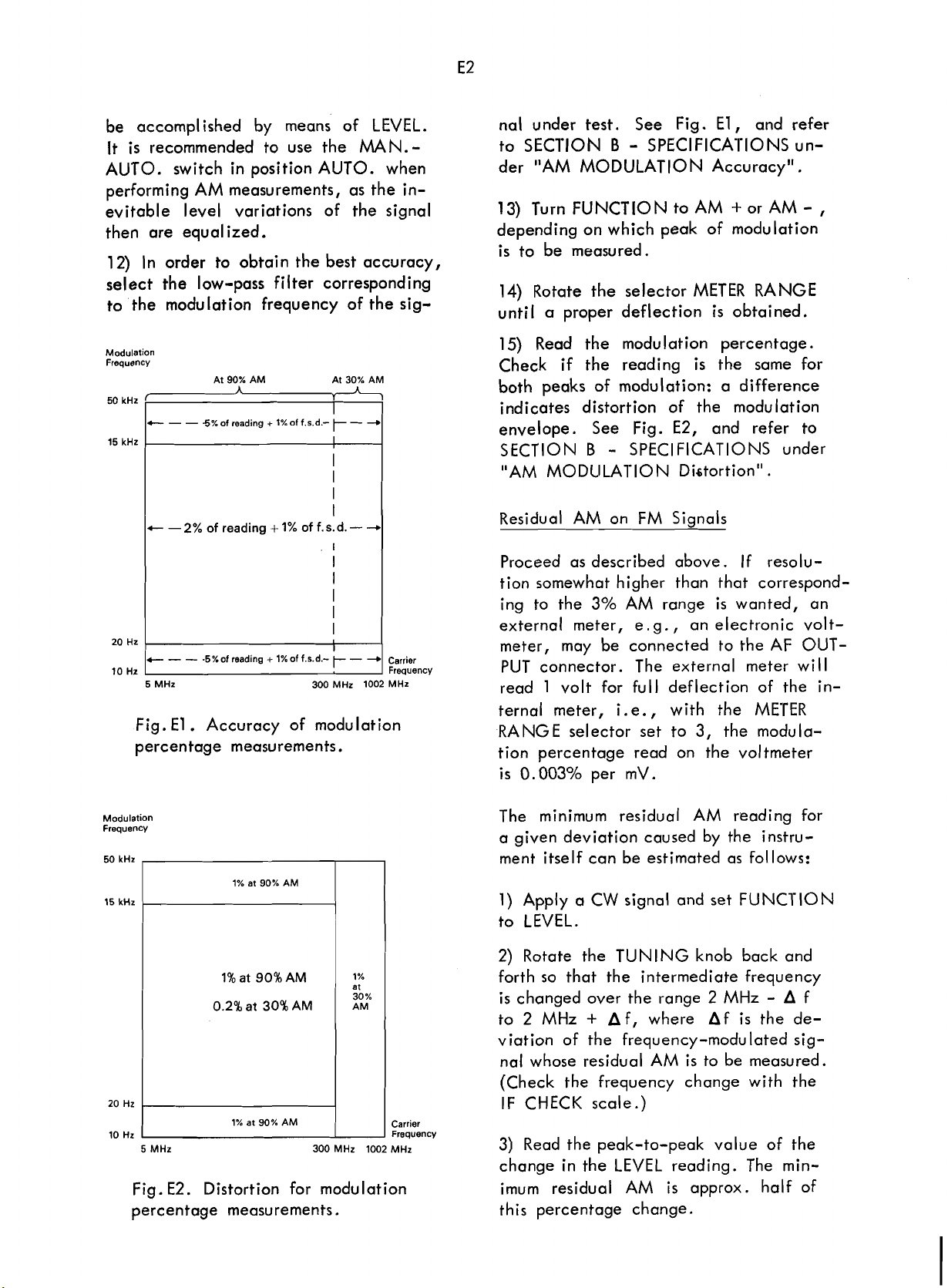
12) In order to obtain
select the low-pass filter corresponding
to the modulation frequency of the
Modulation
Frequency
50 kHz
15 kHz
AM
measurements, as the in-
the
MAN.
best accuracy,
-
sig-
El,
nal under test. See Fig.
SECTION
to
der
"AM
13)
Turn FUNCTION to
depending on which peak of modulation
is
to be measured.
14)
Rotate the selector
until a proper deflection
15)
Read the modulation percentage.
Check if the reading
both peaks of modulation: a difference
indicates distortion of the modulation
envelope. See Fig.
SECTION
"AM MODULATION Distortion".
Residual AM on
B
-
SPECIFICA'I'IONS un-
MODULATION Accuracy".
AM
METER
is
E2, and refer to
B
-
SPECIFICATIONS under
FM
Signals
and refer
+
or AM
RANGE
is
obtained.
the same for
-
,
20 Hz
c
-
-
10 Hz
5 MHz
Fig.
percentage measurements.
Modulation
Frequency
50 kHz
15 kHz
20 Hz
10 Hz
5 MHz
Fig.
percentage measurements.
-5%of reading + 1% of f.s.d.-
El
.
Accuracy of modulation
E2.
Distortion for modulation
-
-+
Carrier
300MHz 1002 MHz
300 MHz 1002 MHz
Frequency
Carrier
Frequency
Proceed as described above. If resolu
tion somewhat higher than that corresponding to the 3% AM range
external meter, e. g., an electronic voltmeter, may be connected to the AF OUT-
PUT connector. The external meter will
read
1
volt for full deflection of the in-
ternal meter,
RANGE selector set to
tion percentage read on the voltmeter
is
0.003% per mV.
The minimum residual AM reading for
a given deviation caused by the instrument itself can be estimated as follows:
1)
Apply
to LEVEL.
2)
Rotate the TUNING knob back and
forth so that the intermediate frequency
is
changed over the range 2 MHz - A f
to 2 MHz
viation of the frequency-modu lated sig-
nal whose residual AM
(Check the frequency change with the
IF
CHECK scale.)
3) Read the
change in the LEVEL reading. The minimum residual AM
this percentage change.
i.e., with the
a
CW
signal and set FUNCTION
+
Af, where Af
peak-t~-~eak value of the
is
is
wanted, an
METER
3,
the modula-
is
the de-
is
to be measured.
approx. half of
-
Page 27
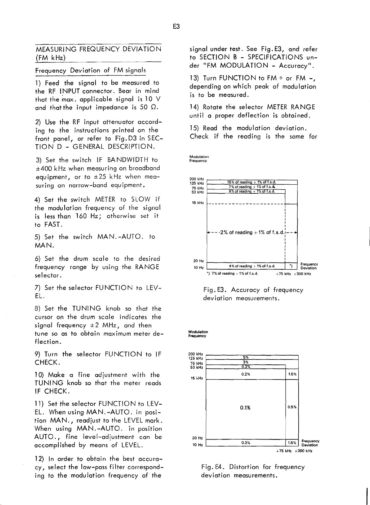
MEASURING FREQUENCY DEVIATION
Scans by ArtekMedia © 2008
(FM
kHz)
FM
Frequency Deviation of
1)
Feed the signal to be measured to
RF
the
that the
and
2)
ing to the instructions printed on the
front panel, or refer to Fig. D3 in SEC-
TION
3)
k400
equipment, or to
suring on narrow-band equipment.
4)
the modulation frequency of the
is
to
5) Set the switch MAN.-AUTO. to
MA
INPUT
hax. applicable signal
thatthe input impedance
Use the
D
Set the switch
kHz
Set the switch
less than 160 Hz; otherwise set it
FAST.
1\1.
connector. Bear in mind
RF
input attenuator accord-
-
GENERAL
IF
when measuring on broadband
k25
METER
signals
is
10
is
50
R.
DESCRIPTION.
BANDWIDTH to
kHz
when mea-
to SLOW if
signal
V
E3,
signal under test. See Fig.
to
SECTIOI\I
"FM MODULATION
der
13)
Turn
depending on which peak of modulation
is
to be measured.
14) Rotate the selector
until a proper deflection
15) Read the modulation deviation.
Check if the reading
Modulation
Frequency
200
kHz
125
kHz
75
kHz
53
kHz
15
kHz
----
---2%
B
-
SPECIFICATIONS un-
FUNCTION
15% of readinq + 1% of f.s.d.
7%of reading + l%of f.s.dr
4%of readinq + 1%of f.s.d.
---
---------
of
reading
+1%
to
FM
METER
is
of
t
and refer
-
Accuracy".
+
or
FM
RANGE
is
obtained.
the same for
I
I
I
I
-,
6)
Set the drum scale to the desired
frequency range by using the RANGE
selector.
7)
Set the selector
FU
NCTlON to LEV-
EL.
8)
Set the
cursor on the drum scale indicates the
signal frequency
tune so as to obtain maximum meter deflection.
9)
Turn the selector FUNCTION to IF
CHECK.
10)
Make a fine adjustment with the
TUNING
52
knob so that the
MHz, and then
TUNING knob so that the meter reads
IF CHECK.
11)
Set the selector FUNCTION to
EL. When using
tion
MAN.,
When using MAN.-AUTO. in position
AUTO., fine level-adjustment can be
accomplished by means of LEVEL.
12)
in order to obtain the best accura-
cy, select the low-pass filter corresponding to the modulation frequency of the
MAN.-AUTO.
readjust to the LEVEL mark.
LEV-
in posi-
20
Hz
10
Hz
')
Fig.
deviation measurements.
Modulation
Frequency
200
kHz
125
kHz
75
kHz
53
kHz
Fig.
deviation measurements.
4%of reading + l%of f.s.d.
7%of reading + 1%of f.s.d. +75
E3.
Accuracy of frequency
E4.
Distortion for frequency
*75
kHz
kHz
Frequency
Deviation
1300
Deviation
*300
kHz
Frequency
kHz
Page 28
both peaks of modulation: a difference
Scans by ArtekMedia © 2008
indicates distortion of the modulating
envelope. See Fig.
SECTION
"FM
B
-
MODULATION - Distortion".
E4, and refer to
SPECIFICATIONS under
Residual
Proceed as described immediately above.
Because of the very effective limiter
stages in the
FM
quite low, viz. 50 Hz (r.m.s.) at 50%
AM when the band-pass filter (50 Hz
15 kHz)
carrier frequency within 15
is
less than 25 Hz
less than 100 Hz
1
002 MHz, when measurements are performed in a room with an acoustical
noise level lower than 60 dB (rel. 2
10-4 pbar) and the band-pass filter
(50
emphases (50 ps or
(See SECTION
If a resolution somewhat higher than
that corresponding to the 3 kHz deviation range
meter can be connected to the AF OUT-
PUT
read
internal meter,
switch set to
thi: electronic voltmeter will be 3 Hz
per
US1
IN UNIT, CODE 900-252
FM
on CW and AM sianals
FM
detector, the residual
caused
Hz
terminals. The external meter will
1
mV.
NG
by
amplitude modulation
is
used. The residual
FM
FM
(r.m.s.) up to
-
15 kHz) or one of the de-
75
B
-
SPECIFICATIONS.)
is
wanted, an electronic volt-
volt for full deflection of the
i.e., with the
3,
the deviation read on
A CRYSTAL OSClLiATOR PLUG-
FM
at a
-
250 MHz
(r. m. s.), and
:IS)
is
used.
METER
is
-
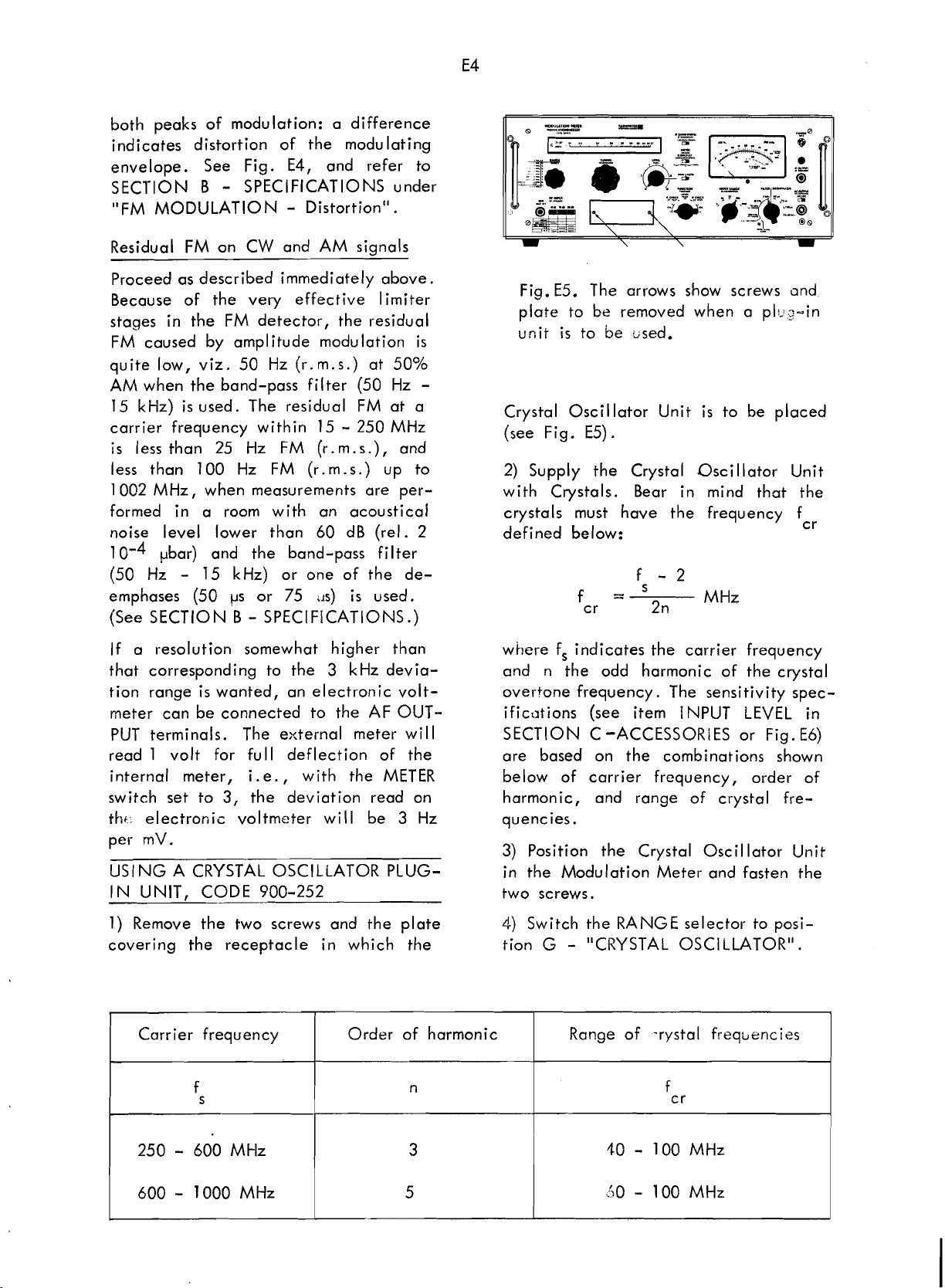
Fig.
ES.
The arrows show screws and
plate to
unit
Crystal Oscillator Unit
(see Fig. E5).
2) Supply the Crystal Oscillator Unit
with Crystals. Bear in mind that the
crystals must have the frequency f
defined below:
where fs indicates the carrier frequency
and n the odd harmonic of the crystal
overtone frequency. The sensitivity spec-
ifications (see item
SECTION C
are based on the combinations shown
below of carrier frequency, order of
harmonic, and range of crystal fre-
quencies.
3) Position the Crystal Oscillator Unit
in the Modulation Meter and fasten the
two screws.
be
removed when a pl!-i.2-in
is
to be used.
is
f -2
f=
c
r 2n
S
-ACCESSORiES or Fig. E6)
MHz
INPUT LEVEL in
to be placed
C
r
1) Remove the two screws and the plate
covering the receptacle in which the
Carrier frequency
Order of harmonic
4)
Switch the
tion
G
RANGE
-
"CRYSTAL OSCILLATOR".
Range of
selector to posi-
-rystal freqbencies
Page 29
5)
Scans by ArtekMedia © 2008
Tune the Modulation Meter to the
desired carrier frequency.
6)
Switch the function selector to IF
CHECK.
7)
Switch
to the desired channel by means of the
four-position selector.
8)
Insert a screwdriver in the hole corresponding to the selected channel, and
adjust the corresponding trimmer until
the meter indicates
the
Crystal Oscillator Unit
IF
CHECK.
9)
If
necessary, repeat steps
until all four channels are trimmed.
10)
'the Crystal Oscillator Unit, code
900-252,
Proceed as described above for
FM
measurements, but keep in mind
that certain specifications of the Modulation Meter proper cannot apply, and
refer to SECTION C under "Change in
Specifications of AFM2 Caused by the
Crystal Oscillator Unit", and see Fig.
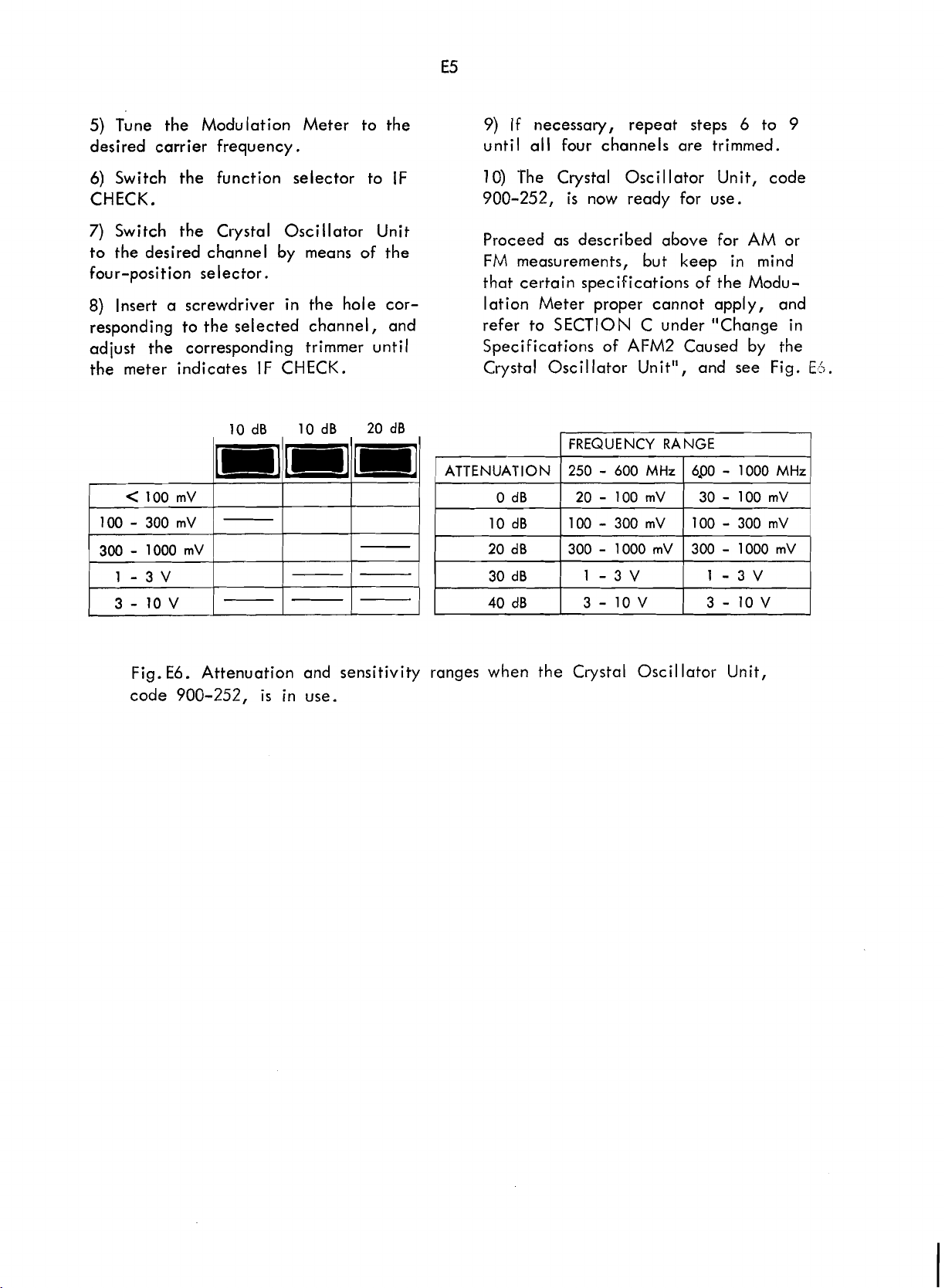
is
now ready for use.
FREQUENCY RANGE
6
AM
to 9
or
E3.
Fig.
E6.
Attenuation and sensitivity ranges when the Crystal Oscil lator Unit,
code 900-252,
is
in use.
AT'TENUATION
0
dB
10
dB
20
dB
30
dB
40
dB
250 - 600
20 - 100 rnV
100 - 300 rnV
300 - 1000 rnV
1
3-1OV
MHz
-3V
6.00
-
1000
MHz
30 - 100 rnV
100 - 300 rnV
300 - 1000 mV
1
-3V
3-1OV
Page 30
Section
Scans by ArtekMedia © 2008
F.
Technical Description
RF
l
NPUT CIRCUIT
RF
The
connector on the front plate of the instrument, then passed through a resistive attenuator
20
which
of the mixer and to adapt the Modula-
tion Meter to
3
mV to 10 V r.m.s.
All
numbered between 1300 and 1399.
TUNER (See diagram No.
The local oscillator consists of (2103 in
a common-base Hart ley
same circuit configuration
ranges. Only the tank circuit
and LA) and the emitter capacitor CA
are exchanged to obtain the different
fundamental ranges from
Up to 200 MHz, the mixing takes place
with the fundamental frequency of the
local oscillator. Mixing with input signals which have a frequency higher than
200 MHz
or 5th harmonics of the local oscillator.
The intermediate frequency
be
used; however, only the lower sideband
can be used at 5 MHz
because the lower frequency limit of
the local oscillator
input signal
dB, 30 dB or
is
inserted to avoid overloading
RF
components of the
is
accomplished with the 3rd
2
MHz, and both sidebands can be
is
fed to the BNC
(~rovidin~ for 10 dB,
40
dB attenuation)
signals in the range
RF
attenuator are
1)
coupl ing . The
is
used in all
(CC, CB,
7
to 200 MHz.
is
chosen to
RF
input signal
is
7
MHz.
With the selector
CRYSTAL OSCILLATOR, the local os-
cillator
lator providing for operation at a fixed
frequency, such as the Crystal Oscil-
lator Unit, code
The signal from the
that from the local oscillator or the
Crystal Oscillator Unit are fed to the
diodes
balanced mixer and provide for good insulation between the input terminals and
the local oscillator or the Crystal
cillator Unit, and thereby reduce the
influence of stray radiation. The resulting 2 MHz signal
via
The tuner lias its own current limiters,
i.e.,
-12
Al l components of the tuner are num-
bered between 100 and 199.
IF
The output impedance of the mixer
matched capacitively to that of the
filter. In this fashion, variations of the
output impedance of the mixer become
uncritical. From
frequency signal of
a band-pass filter which
mixing products.
type, and it has a bandwidth of
is
disconnected, and an oscil-
CRlOl to CR104 which form a
T102.
QlOl
for +12
v.
FILTER (See diaaram No. ll)
RANGE
900-252, may be used
RF
is
fed to the
V,
TI
02, the intermediate
2
It
is
in position
attenuator and
Os-
IF
filter
and Q102 for
is
IF
MHz passes through
reiects unwanted
of the phase-linear
*400
Page 31

kHz
Scans by ArtekMedia © 2008
around the intermediate frequency.
A
high
degree of phase-linearity
essary to achieve measurements on FM
signals with minimum distortion, especial-
ly when the modulation frequency
All
components of the
bered between 200 and 299.
IF
PREAMPLIFIER
(See diaaram No.
The three-stage IF preamp1 ifier consists
Q301,
of
the IF filter against load impedance variations from the
same time, it provides for amplification
before the signal
uator. Amplification alongside with an
glmost ideal connection to the
results in a minimum amount of noise at
all input levels. The ohmic part of the
IF amplifier input
of
R304,
of
C306. The amplified
fed to the
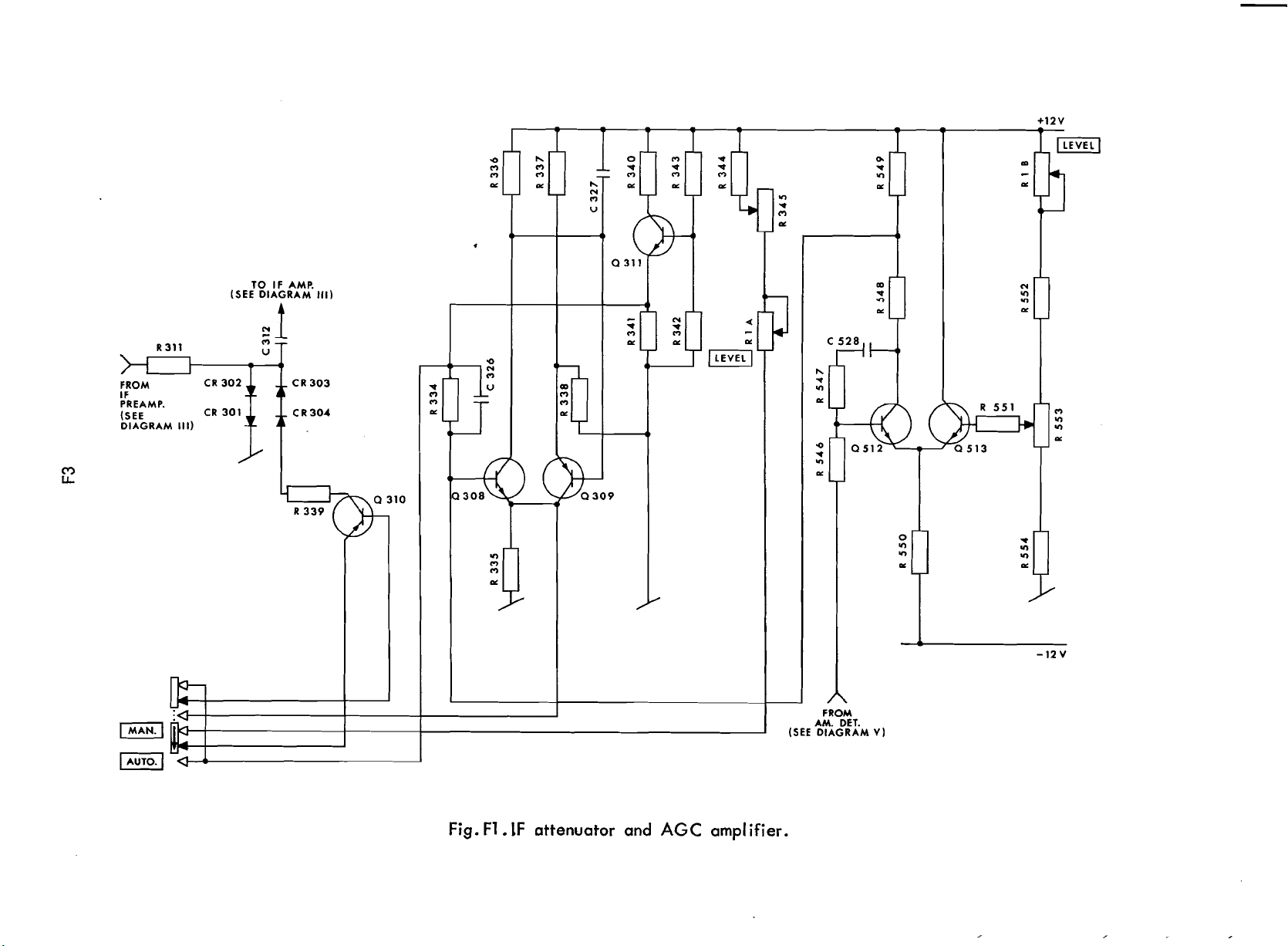
The IF attenuator (see Fig. F1) consists of
R311 and the four diodes
R311 and the four diodes form
divider with one fixed resistance and the
variable resistance resulting from the combination
Combining these four diodes ensures linear
characteristic and thereby minimum distor-
tion. The resistance value resulting from
the above combination depends on the
biasing current of the four diodes.
biasing current
tor of the current generator
sition
the base of
termined by the reference voltage source
Q311.
thereby its collector current,
by means of the potentiometer
EL)
accessible from the front of the instrument.
biasing current of the diode complex
CR301 to CR304, and, therefore, in regulation of the
sitivity of the
RF
input voltage can be adiusted
means of R345.
Q302, and
IF
and the reactive part by means
IF
attenuator via C308.
CR301
MAN.
The emitter current of Q310, and
This
-
is
of the MAN.-AUTO switch,
Q310
results in regulation of the
IF
level. Finally, the sen-
IF
attenuator at a given
IF
filter are num-
AND
Ill)
IF
ATTENUATOR
(2303.
attenuator. At the
is
fed to the
is
matched by means
IF
signal
CR310 to CR304.
CR302
drawn from the collec-
//
CR303 - CR304.
Q310.
is
at a potential de-
is
nec-
is
high.
It protects
IF
atten-
IF
filter
is
then
a voltage
This
In po-
is
control led
RIA
(LEV-
by
When the switch MAN.-AUTO.
position
a voltage delivered
fier. The AGC
differential amplifier Q512 and Q513
followed by a unity-gain amplifier
and Q309. The base of Q513
potential determined by the divider consisting of
R554. The base of Q512 receives a signal proportional to the
AM
any)
Q308) of the unity-gain amplifier driv-
ing the exponential amplifier
The emitter of Q310
provided by the voltage reference source
(3311 . the emitter basis ;oltage of Q310,
and thereby the biasing current of the
diodes
control led by the potentiometer
(LEVEL)
All components of the
and
300 and 399.
IF
AMPLIFIER (See diagram No. ll
The signal from the
then fed to the
sists of the two
stages
'The
a voltage level higher than that required by the
provides for compensation of the attenuation in the following band-pass filter
or phase-compensator
All
numbered between 300 and 399.
PHASE-COMPENSATOR AND
PASS
the amplified
a phase-compensator or to a band-pass
filter, according to the position of the
IF
BANDWIDTH switch. When the
BANDWIDTH
the phase-compensator
It provides for compensation of the
error that arises in the
phase error
AUTO.,
R1
detector. The difference signal
is
then fed to the input(base of
CR310 to CR304,
and by the AGC amplifier.
IF
attenuator are numbered between
Q304, Q305 and Q306,
IF
amplifier brings the
the base of
by
the AGC ampli-
amp1 ifier consists of a
B
(LEVEL),
IF
wideband amplifier
R552, R553, and
IF
level from the
is
at a voltage
is
in this case
IF
preamplifier
IF
attenuator
amplifier which con-
IF
AM
detector and thus
.
components of the IF amplifier are
FILTER
(See diaaram No.
IF
signal
is
in position rt400 kHz,
is
due to the theoretical
is
then fed to
is
switched in.
IF
filter.
is
in
Q310
is
is
Q308
at a
(if
Q310.
RI
B
I)
is
Q307.
signal to
BAND-
lM
IF
phase-
This
at
Page 32
Scans by ArtekMedia © 2008
Page 33

asymmetry of the
Scans by ArtekMedia © 2008
around the intermediate frequency. In
the position
WIDTH switch, the band-pass filter
switched on. It
IF
the
but has a bandwidth of h25 kHz, and
is
signals from narrow-band equipment.
BUFFER AMPLIFIER (See diagram N0.V)
The signal from the phase-compensator
or the band-pass filter
fer amplifier which separates filter,
detector, and output amplifier. It consists of a two-stage unity-gain amplifier
(Q501 and Q502) and serves to suppress
any influence from the
signal from the buffer amplifier
both to the
output
filter concerning phase-linearity
intended for use when measuring on
AM
ampi ifier.
IF
filter characteristic
h25 kHz of the
is
of the same type as
is
IF
detector and to the IF
IF
fed to a buf-
output. The
BAND-
is
AM
is
fed
,
first low-pass filter section
C710 and C711 on diagram
the network consisting of
R539, and C530. R539
brate the AM detector.
Note: The low-pass filter and the following AF section are described below.
All
the components of the AM detector
are numbered from
IF
OUTPUT AMPLIFIER (See diagram
500 to 599.
(L701, L702,
VII),
R537, R538,
is
used to cali-
via
N0.W
The signal from the buffer amplifier
also fed to the IF output amplifier which
consists of the four stages
Q505, and (3506, and which provides
for amplification of the
level required by the following limiter
stages. The two diodes
are used to protect the limiter input stage
high
against too
a voltage.
(2503, Q504,
IF
signal to the
CR502 and CR503
is
All
components of the Buffer amplifier
are numbered between 500 and 599.
AM DETECTOR (See diagram N0.V)
The signal from the buffer amplifier
fed to the
a three-stage amplifier
and Q509 with a mean-value detector
CR505 and CR506 in the feedback loop.
The feedback ensures a good linearity.
A pair of output transistors, Q510 and
Q511, provides for two outputs. The
signal on the collector of
portional to the
fed via R546 to the differential amplifi-
er which
setting circuitry (described above), and,
via R543 and
plementary
Q515, forming a dc output amplifier
delivering voltage to the
output. The signal from the collector of
Q511
dicating meter which provides for check-
ing of the IF level.
The signal on the collector
detected signal which
AM
detector. It consists of
Q507, Q508,
Q511
IF
level.
is
part of the automatic level
R555, to a pair of com-
emitter-fol lowers, Q514 and
is
also fed via R544 to the in-
This
IF
LEVEL
Q510
is
fed through a
is
pro-
signal
(DC)
is
is
is
the
All components of the
fier are numbered between 500 and 599.
LIMITER
Genera
The amplified
of three limiters.
All components of the limiter stages are
numbered from 600 to 699.
First limiter stage.
The first limiter stage consists of two
emitter-coupled transistors, Q601 and
Q602. Their working point
by the current delivered
dc current generator
IF
signal from the
fed to the base of Q601, wh t 1st the base
of Q602
a sufficient
and Q602 are cut-off, and the output
voltage of the first limiter (at
a square-wave. The peak-to-peak value
of this square-wave
stant current generator Q607. The first
limiter
circuit which holds the zero-crossing of
the square-wave output voltage. The
regulation circuit consists of a
STAGES
I
IF
signal
is
connected to ground. When
IF
level
is
provided with a regulation
IF
output ampli-
(See diagram No.
is
fed to a series
is
determined
by
the constant
Q607. The amplified
IF
output amplifier
is
reached, Q601
C605)
is
fixed by the can-
peak-dif-
VI)
is
is
Page 34

ference detector, CR601 and CR602, and
Scans by ArtekMedia © 2008
a differential amplifier, Q603 and
where any signal from the peak-difference
detector
ponent of the square-wave. The output
signal of the differential amplifier (if
any)
Q602 via the two emitter-fol lowers Q605
and
Subsequent l imiter stages
From
fed to two subsequent limiter stages
Q608-(2609 and Q610-Q6ll where it
is
again limited. The resulting signal
then fed to the
FM DETECTOR (See diagram No.VII)
The
mu1 tivibrator and an output stage.
The multivibrator consists of
Q702. It
positive pulses from the last
stage.
base of Q701 via
is
cut-off when no
to its base whilst transistor Q702 conducts, and conversely.
is
compared with the dc com-
is
fed to the bases of Q601 and
Q606.
C605, the square-wave signal
FM
detector via Q612.
FM
detector consists of a monostable
(2701 and
is
triggered by the train of
I
imiter
This
train of pulses
C701. Transistor Q701
IF
is
signal
fed to the
is
Q604,
is
is
applied
is
then passed, via a low-pass filter
consisting of
C711, to the
low.
A positive voltage, varying proportionally to the modulating frequency,
drawn from the collector of (2704 and,
via R726 and
amplifier stage consisting of the double
transistor Q709 and
The amplifier signal present on the
emitter of Q711
IF
FREQ.
part
is
fed via R736 to the meter when
the selector FUNCTION
position. R737 and R739 provide for
fine adjustment of
and gain.
The monostable
'
output
own +10
supplies. 'they consist of
Q615 and Q616 for +10
Q618, Q619 and Q620 for -10
(See diagram
All components of the
numbered between
stage are provided with their
L701, L702, C710 and
AF
section described be-
is
R727, fed to a unity-gain
Q710 and Q711.
is
fed via R734 to the
(DC) output, whilst the other
is
in
IF
CHECK
IF
CHECK position
mu1 tivibrator and the
V
and
-1
0 V regulated power
Q613, Q614,
V,
and Q617,
V.
VI)
FM
detector are
700 and 799.
multivibrator has a time-constant
The
determined by
and it delivers a square-wave signal
across
the output stage which consists of
and
two transistors of the output stage are
determined by the constant dc current
generator
square-wave
amplified in Q705 and
turn drive the constant-current generator
Q708 via Q707, thereby regulating
amplitude variations. As the width of
the pulses and their amplitude are constant, the mean value of the output
voltage of the output stage will vary
according to the number of pulses per
second of the square-wave,
cording to the modulating frequency.
Frequency-modulation of the
will cause a variation of the output
voltage of the output stage.
R702. The positive pulses drive
Q704.
R707, R708 and C703,
Q703
The working points of the
Q708. The peak value of the
is
detected by CR704 and
(2706, which in
i
.
e., ac-
IF
signal
This
signal
AF AMPLIFIERS
(See diagram VI 11)
The signal from the AM detector
to the second low-pass filter, consisting
of
L801, L802, L803, L804, L805, C801,
C802, C803 and C804, when the selector
FUNCTION
AM. The signal from the
is
fed to the second low-pass filter
when the selector FUNCTION
of the positions
is
characterized by its good phase-
linearity and its almost flat frequency
response, which are both required for
passing a stereo signal with minimum
distortion.
The filtered signal
the first section of a two-section resistive AF attenuator (see diagram
and fed fo the first
which consists of
Q803.
I
AND
is
in one of the positions
FM.
Q801, (2802, and
I
I
FM
detector
is
The low-pass filter
is
then passed through
AF
AMPLIFIER,
is
in one
XII)
fed
Page 35

The amplified signal at the collector of
Scans by ArtekMedia © 2008
Q803
of the
and fed to the second AF AMPLIFIER,
which consists of
Q806.
amplification and for the low output
pedance required for coupling to the
subsequent low-pass filter
All components of the AF AMPLIFIERS
I
AF AMPLIFIERS
The amplified signal from amplifier
fed to the low-pass filter, which con-
sists
C902, and which provides for limitation
of the noise bandwidth in the AF section of the instrument without deterioration of the phase-linearity and
response.
The filtered signal
the third AF amplifier.
amplifier, consisting of Q901 and
which
in when the
is
15
other positions of the
selector. For filter characteristics, see
SECTION
emphasis networks and the
are regular RC networks.
The following AF amplifiers IV and V,
consist respectively of
Q906, Q907, and Q9Q8, Q910, Q911 and
is
passed via the second section
AF
attenuator (see diagram XII)
04,
It
provides for the necessary
'3805 and
.
and
II
are numbered from 800 to 899.
Ill
-
V (See diagram
of L901, L902, L903, C901, and
frequency-
is
then passed through
It
is
a unity-gain
is
part of the active filter switched
FI LTER/DEEMPHASIS selector
in
position 3 kHz, 15 kHz and 50 Hz
kHz
(3
dB).
It
acts as a buffer in the
FILTER/DEEMPHASIS
B
-
SPECIFICATIONS. the de-
6
dB/oct filter
Q903, Q904, Q905,
im-
1X)
II
is
Q902,
-
Q912. They bring the signal up to the
level required by the AF detector.
is
The AF OUTPUT signal
the emitter of
AF
OUTPUT switch
and via R920 and C911 when the AF
OUTPUT switch
All the components of the AF amplifiers
111
-
V
are numbered from 900 to 999.
AF DETECTOR (See diagram X)
The signal from the emitter of
fed to the AF detector which consists of
diodes
is
of modulation, whilst diode
for detection of the positfve modulation
peaks. Selection of the peak of modulation (positive or negative)
means of the FUNCTION selector in
the positions AM or FM.
The detected signal
impedance converter so that
fed to the
and to the meter.
All the components of the AF detector
are numbered from
BOWER SUPPLY (See diaaram
The power supply provides for the regu-
lated dc voltages (-12 V,
required by the different sections of the
instrument. (For -10 V and +10 V sup-
ply, see FM DETECTOR.)
All the components of the power supply
are numbered from 11
CRl 001 and CR1002. Diode CR1002
used for detection of the negative peaks
C907 via R920 when the
is
is
in position AC.
is
MOD.LEVEL (DC) output
1000 to 1099.
drawn from
in position DC,
(2912
CRl 001
is
done by
then fed to an
it
can be
XI)
0 V, +12
00 to 11 99.
is
is
V)
used
Page 36

Section
Scans by ArtekMedia © 2008
G.
Maintenance
The following maintenance procedure
found defective
factory.
instruments necessary to make these field
the required
TEST
The following
specifications and should possess the
Signal generators (referred to in the text
This
INSTRUMENTS REQUIRED
is
replaced by a new one delivered by Radiometer and prealigned at the
procedure reduces adjustments in the field to a minimum. However, the test
standard of performance of the
is
a
list
of preferred instruments. Any alternatives must have equivalent
is
same degree of accuracy.
based on the assumption that
adjustments must be of high quality to achieve
my
printed circuit
AFM2.
as
Sig-Gen.) to cover
5
-
1000
MHz,
50
R
impedance,
1
Hewlett Packard
1
Hewlett Packard
1
Hewlett Packard
AF
1
1
1
1
1
Oscillator, for example': Radiometer BKFIO, distortion
the text as
Oscilloscope, for example, Philips PM3231
DC
DVM (digital voltmeter), Hewlett Packard 3403A
AC
DVM, Hewlett Packard 3430A
AC
VTVM,
as
follows:
606B
(50 kHz-65 MHz)
608E
(1
0
MHz-480 MHz)
612A (450 MHz01230 MHz)
AF
Osc.)
Hewlett Packard 400E or equivalent
(I%,
<
0.01% (referred
with scales calibrated in rrns)
to
in
Page 37

Miscellaneous
Scans by ArtekMedia © 2008
1
Resistor, 500
2
Resistors, 10
2
Resistors,
1
$2
0.1
kQ
f
0.1%, 0.25
MQ
*0.1%, 0.25
%,
0.25
W,
precision carbon film
W,
precision carbon film
W,
precision carbon film
Capacitor, 0.47
1
Hexagonal Key, 2.5
1
DISMANTLING
To remove the
Stand the instrument on its rear
a)
Remove the four hexagonal
b)
Carefully lift the instrument out of the case.
c)
PRELIMINARY
)rF
AFM2
(30 V wkg.
mm
(at least 75
from its case proceed as follows:
is
bolts
suitable)
mrn
in length)
panel.
located beside the carrying handles on the front panel.
Prepare the following
Refer to
a)
f
0.1
Prepare an attenuator
b)
REPLACEMENT AND REALIGNMENT PROCEDURE
TUNER printed circuit board
Fig.G4 shows the location of the TUNER and Fig.
1)
assembly.
Fig.Gl and connect two 1
%
resistor in parallel and connect the 0.47
item:
or
shown in Fig.
M2
*O.
G2
T%
from
OF
resistors in series. Connect a 500
pF
capacitor
two
10
kR
THE PRINTED CIRCUIT BOARDS
G5
shows a top view of the TUNER
as
shown.
h
0.1 % resistors.
R
To remove the
2)
(pry
UP).
TUNER
printed circuit rotor, first remove the cover plate of the TUNER
Page 38

Remove the 7 screws retaining the circular printed rotor. Carefully pull the rotor out
Scans by ArtekMedia © 2008
3)
of the fixed contacts and then lift out. Replace the new rotor in the opposite sequence.
Check the orientation of the rotor and take extreme care not to damage the contacts
4)
5)
6)
7)
on the fixed printed circuit board. Before securing the
the rotor does not foul the fixed printed circuit
centred and
To remove the fixed TUNER printed
Remove .the
Turn the TUNING knob fully counterclockwise.
Insert a
plate and loosen the set screw in the coupling of the variable capacitor.
Unsolder the
care not to
heat when
that
the contacts mesh correctly (no overlapping of the contacts).
circuit board, proceed
TUNER
2.5
mrn
10
damage the leods or the cable insulation. Do not use excessive
unsoldering these connections.
printed circuit rotor
hexagonal key through the hole in the bottom chassis support
leads
and
cables soldered to the printed circuit board, taking
as
board.
described in
7
retaining screws, check that
Check that
cis
3)
above.
it
follows:
is
properly
.
8)
9)
10)
11)
12)
13)
Remove the three screws securing the printed circuit board.
Using the blade of a screwdriver
support, hold the coupling in place and carefully pull out the printed circuit
inserted
through the hole in the bottom chassis
board.
To replace the printed circuit board, proceed
Again using the blade of a screwdriver inserted through the hole in the bottom
chassis support, guide the coupling into position over the variable capacitor shaft
and mount the printed circuit
lnsert the three retaining screws, but
Mount the printed circuit rotor as described above in
boad
into place.
do
as
follows:
not tighten them
3).
at
this
point.
14)
15)
Secure the three retaining screws when both the rotor
boarcls are orientated correctly.
Rotate the variable capacitor until fully meshed.
and
fixed printed circuit
Page 39

16)
Scans by ArtekMedia © 2008
Tighten the screw in the coupling, using the
2.5
mm hexagonal key.
17)
18)
19)
20)
21)
Proceed to the electrical adiustments as follows:
Set the following controls:
RANGE switch to A
7
TUNING to
IF BANDWIDTH to &400 kHz
MAN./AUTO switch to
FUNCTION switch to LEVEL
LEVEL potentiometer fully clockwise.
Connect the Sig. Gen.
Set the Sig. Gen. to
Adjust the Sig. Gen. output until a suitable indication on the
AFM
is
obtained.
MHz
MAN.
(HP606B)
9
MHz.
to the
RF
INPUT connector of
th
AFM2
METER
of the
22)
23)
24)
25)
'
26)
Using a trimming tool, adjust the oscillator coil for
circular printed circuit rotor) for a
METER
is
Reset the Sig. Gen. to 10 MHz.
Reset the
Using a trimming tool, adjust the oscillufor trimming
(located next to the oscillator coil for
the
Because of interaction between these adiustments, it will
22) to
respective TUNING settings without readjustment.
overshoots, turn the
obtained.
TUNING
METER.
25)
inclusive several times until the maximum deflection occurs at the
to 12
LEVEL
MHz.
maximum deflection on the
knob .anticlockwise until a suitable deflection
RANGE
RANGE
capacitor
A)
for a maximum deflection on
A
(marked on the
METER.
to
RANGE
be
necessary to repeat
If
the
A
27)
Repeat
range frequencies, choosing the Sig. Gen. necessary to cover the range in
).ion.
.17)
to 26) on the remaining ranges
B,
C,
D,
E
and
F
at
the appropriate
ques-
Page 40

IF
Scans by ArtekMedia © 2008
FILTER (WIDE) and
IF
AMPLIFIER/IF ATTENUATOR printed circuit boards
These two printed circuit boards are matched at the factory and must
a matched pair. No realignment adjustments are necessary.
-
the
IF
28)
29)
30)
.31)
32)
33)
To replace
Remove the cover plate by unscrewing
Unsolder the input and output cables to the printed circuit board, taking extreme care not
Using a fine-blcded angle screwdriver, unscrew the four screws securing the
printed circuit boad to the housing.
Lift the printed circuit board out.
Replace in the opposite sequence, again taking extreme care when soldering the
input and output cables.
FILTER (WIDE) proceed
to
damage the cables or the nearby componentsF by overheating.
as
thi
four screws
follows:
A
(two shown in Fig.G7).
be
replaced as
4
34)
When IF
board
at
the factory in pairs.
35)
36)
37)
IF
To change out the
C
by
it
can
The printed circuit board may then
when disengaging the multiconnector.
When replacing the board, first make sure that
tion and then slide it into the guides.
gaging the multiconnector. Make sure that the board
FILTER (NARROW) printed circuit bod
FILTER (WIDE)
must also
loosening the two screws
be
lifted over the screws.
be
is
replaced, the IF AMP/ATTENUATOR printed circuit
changed out (or vice versa),
IF
AMP/ATTENUATOR
D
shown in
be
board,
Fig.
withdrawn.
Same
resistance will
as
these two boads are matched
first remove the retaining bar
G7
and sliding the bar until
it
Some
is
resistance will
located in the correct ,posi-
be
felt when en-
is
pressed fully in.
be
felt
38)
No recrltgnment
M.
adjustments
are necessary when replacing this printed circuit
-
Page 41

G6
Scans by ArtekMedia © 2008
AM DETECTOR
39)
40)
41)
42)
Connect the DC DVM to the IF
Turn the LEVEL potenttometer counterclockwise.
Adjust pdentiometer R558 (see Fig.G6)
Disconnect the DC DVM.
-I.
IF AMPLIFIER printed circuit
43) Set the FUNCTION switch
44)
45)
46)
Set the METER RANGE switch to
Set the
FILTER/DEEMPHASIS switch to 50 Hz-15
Check that the MAN./AUTO switch
to
LEVEL
LEVEL.
3
and
is
board
@C)
still
jacks.
until
the DC DVM indicates 0
IF BANDWIDTH to
the
kHz.
set
to
MAN.
1
*400
.
V
t2.
kHz.
mV.
47)
Remove the cover of the TUNER
Fig. G5.
48)
49)
50)
Connect the output of the Sig.
to
2
Set the Sig. Gen.
AFM2 deflects to the LEVEL
the
Note the
outpvt level on the Sig. Gen. and then reduce this output by
MHz
k1 kHx
(20 dB).
51)
Set the
MAN./AUTO switch to AUTO.
52) Set the LEVEL potentiometer to 5.
53)
Adjust
to the LEVEL
the
potentiometer R553, shown in Fig,G6. until the METER again deflects
mmk.
(pry
up) and unsolder the cable
Gen, to the cable.
and
adjust
mark.
the output until the METER on
W2,
shown
10
in
times
,
54)
Disconnect the
plate.
Set
55)
the MAN./AUTO switch to MAN. and the IF BANDWIDTH to
Sig.
Gen.
and
reconnect the cable
W2.
Replace the TUNER cover
20
kHz.
Page 42

56)
Scans by ArtekMedia © 2008
Connect an oscilloscope to terminals
J500/5
and
J500/6 (0
V).
,..
57)
58)
59)
60)
61)
62)
63)
Connect the Sig. Gen. to the
Set the RANGE to scale
Set the
Adjust the output of the Sig. Gen. until the
the
Adjust the oscilloscope and check that the display shows a sine waveform.
Turn the
mencement of
Ad just potentiometer
form are symmetrical with respect to the x-axis,
LEVEL
LEVEL
LEVEL
potentiometer to about half way.
mark.
potentiometer clockwise until the display just shows the com-
"flats"
A.
on the peaks of the display.
R514,
RF
INPUT socket and set the frequency to
shown in Fig.
METER
G6,
until the "flats" on the
on the AFM2 deflects to
2
sine
MHz.
wave-
Set
IF
64)
65)
66)
t
67)
68)
Set Sig. Gen. to
output level should
Carefully unsolder the cable
Connect the prepared assembly shown
Connect point
Connect point B to tag
Connect point C to the centre conductor of cable
Withdraw the
short circuit across the capacitor
.
BANDWIDTH to
A
to tag 8 on
AF
AMPLIFIER
12
be
*4400
MHz
about
16
kHz.
with an
30
mV.
W16
J700
on
J800.
1-11
printed circuit board and connect a temporary
C805.
AM
modulation of
from terminal
in
Ftg.G1
(See
J800/16.
cn
Fig.
I
kHz
at
about
(AF
AMPLIFIER
follows:
W16.
H8
for location.) Replace the
30%.
1-11,)
The
board
69)
Withdraw the
Roceed
back into the
AM
as
follows:
AFM.
DET.
printed circuit
board
and refer to Figs.G3
and
H5.
Page 43

Temporarily disconnect strap A on tag block
Scans by ArtekMedia © 2008
TB501.
70)
71)
72)
73)
74)
75)
Tempororfly connect straps C and
Replace the
Set FILTER/DEEMPHASIS to
Set METER
Set
MAN./AUTO
Connect the DC
Set
the FUNCTION switch to
METER
the
Set the FUNCTION switch to
METER
RANGE
on
on the
board
the
AFM2
back into circuit.
3
kHz.
switch to 100.
switch to AUTO.
DVM
between the points A and
LEVEL
AFM2
deflects to the
deflects to the
IF
D.
B,
shown
and adjust .the
LEVEL
CHECK and adjust the TUNING knob until the
IF
CHECK mark,
LEVEL
mark.
in
Fig.GI.
potentiometer until
.
76)
77)
78)
79)
80)
81)
Set the
shown in Fig.G6,until the
ferred to
Connect the
Now connect the attenuator shown in Fig.G2
connecting point D to the centre conductor and point
Connect the AC
Set the MAN./AUTO switch to
the
Now note the voltage indicated on the
as
to
AC
U2,
VTVM
FUNCTION
as
Ul
.
AC
VTVM
VTVM
indicates the same value as was noted in
mitsh
to
+AM
DC
to the
between points E and F.
and odjurt the trirnmr potentiometer R539,
DVM
AF
OUTPUT
MAN
indicates
and adjust the LEVEL potentiometer until
93.9
connector and note the value obtained.
to the
DC DVM.
This
mV. This value will
AF
OUTWT
F
to the outer screen.
77)
above.
value will
connector,
be
referred
be
rc-
If
83)
U2-U1
R539
is greater than 94.9
untfl the value
indicated
by
a value x (i.e. U2-U1
by
the
DC
DVM
L:
=.93.9 rnV-
94.9
x.
+x),
readjust
Page 44

84)
Scans by ArtekMedia © 2008
Repeat 83) until
U2-U1
r
94.9 mV.
85)
86)
87)
IMlTER printed
L
88)
89)
Disconnect the DC DVM and the
AF OUTPUT socket.
the cable W16 to tag 16 on 5800.
Replace the strap A and disconnect the
the AM DETECTOR printed circuit
Disconnect the short circuit across C805
board.
Connect the DC DVM between tags
Using
AC
WVM. Remove the attenuator from the
Unsolder the assembly from J700/8-J800/16 and resolder
strap C and D (shown in Fig.G3) on
krd.
on
the AF AMPLIFIER printed
circuit
a
trimming tool, adjust potentiometer R660, shown. in Fig.G7, until the
'board
15
(0
V)
and 16 on 5600 (LIMITER).
circuit
90)
*
91)
92)
93)
94)
95)
4-1
DC DVM indicates
.Disconnect the
Set
the FUNCTION switch to LEVEL.
Set the
Set
Set
Locate the FM Detector printed circuit
METER
the
IF
the FILTER/bEEMPHASIS switch
DC
RANGE
BANDWIDTH to *400 kHz and the MAN./AUTO switch to MAN.
0 V- dc 10.5%.
DVM.
switch to 3.
to
50
Hz
-
15
kHz
and the RANGE to
board and unsolder the centre conductor
A.
of cable W9
96)
Solder the assembly shown in Fig.
point
at
B
to tag 8 of
tag
5
on
S700.
5700.
GI,
as
follows: Point A to tag' 5 of
Point C on the assembly
is
not used in this check.
JN)O
and
Page 45

97)
Scans by ArtekMedia © 2008
Connect the
DC
DVM
between tag 8 of
.I700
and point H of the assembly.
98)
99)
100) Reset the FUNCTION to
101)
102)
Connect the
Set FUNCTION to IF
TER
indicates the IF CHECK mark. Reset FUNCTION to
LEVEL
Using a trimming tool,
the
Disconnect the DC
of cable
pot. until the
DC
Sig. Gen. to the RF
METER
DVM
indicates 955 mV.
DVM
W9.
CHECK
INPUT
and
tune the
indicates the level mark.
and mt the
AFM
(about
frequency
8
MHz)
LEVEL
to
i0
MHz.
until the
and diust the
ME-
-FM.
djust the potentiometer R708, shown in Fig.G6, until
and
resistance assembly. Reconnect the inner conductor
IF
CHECK realignment adiustments
103)
104) Set the
105)
106)
107) Reset the FUNCTION switch to IF CHECK.
108) Using a trimming tool, adjust the potentiometer
Set the Sig. Gen. to
LEVEL
Set
the FUNCTION switch to
Adjust the output level of the Sig. Gen. until the
mark on the scale.
the
METER
potentiometer to position 10.
deflects to the IF
2
MHz.
LEVEL.
CHECK
mark.
METER
R737, shown in Fig.G7, until
deflects to the
LEVEL
109)
1
10)
Vary the
the deflection on the
mark,
Disconnect the
t
10
2
MHz
kHz.
setting of the Sig. Gen. by + and
Sig.
METER
en.
corresponds to + and
-
-
200
200
kHz
and
check that
kHz
from the IF CHECK
Page 46

AF AMPLIFIER
Scans by ArtekMedia © 2008
1-11
prlnted circuit board
--
11
112)
113)
114)
115) Connect the
116)
-
117)
118)
Withdraw the AF AMPLIFIER Ill-V printed circvit board.
1)
Unsolder the centre conductor of cable W15 from tag 15 of
Set
the FILTER/DEEMPHASIS to 6 dB/oct.
Set the METER RANGE to
Using
the
DC
Replace the AF AMPLIFIER Ill-V printed circuit board, and resolder
Adjust the AF AMPLIFIER Ill-V printed circuit board
J800.
3.
DC
DVM between the tags 2 and
a
trimming tool, adjust the potentiometer R803, shown in Fig.G6, until
DVM indicates 0 V * 10 mV.
3
(0
V) of
5800.
4
W15
as
set out in 120) to 131)
in place,
below.
119)
AF AMPLIFIER Ill-V minted circuit board
120)
121)
122)
123)
124)
Adjust the AF DETECTOR printed circuit board as
Set
FUNCTION
Set
METER
a
Using
METER on the AFM2 indicates zero.
Set the METER RANGE to 30.
Set the
trimming tool, adjust potentiometer R929, shown in Fig.G6, until the
FILTER/bEEMPHASIS switch to 200
to +AM.
RANGE to 100.
kHz.
set
out
in
132) to
134)
below.
125)
126) Connect the AC DVM between tags 15 and
Connect the AF Osc. between
the frequency to 1
kHz.
tags 4 and
6
(0
18
V)
on 5700
(0
V) dn J8004(AF
(FM
DET.) and set
AM
1-11).
Page 47

127)
Scans by ArtekMedia © 2008
Adjust the output of the AF Qsc. until the AC DVM indicates 20
mV rms.
128)
129)
130)
131)
AF DETECTOR printed circuit
132)
133)
Disconnect the AC DVM and reconnect it to the AF OUTPUT connector.
Using a trimming tool,
'AC DVM indicates 0.672 V (rrns value).
Using a trimming tool,
the
METER
Disconnect the AF Osc. and the
Set the FUNCTION switch to
Set the
on
the
METER
RANGE
AFM2
ad
just potentiometer R909, shown in Fig.
adjust the potentiometer R923, shown in Fig.G4, until
indicates 30.
AC
DVM.
boad
G4,
until the
-AM.
to 100.
134)
POWER
135)
RF
136) No realignment
Using a trimming tool,
METER
SUPPLY printed circuit
No realignment is necessary after replacing the POWER SUPPLY printed circuit
board.
ATTENUATOR printed circuit
board.
on the
AFM
is
ad
just potentiometer R1002, shown in Fig.G7, until the
indicates zero.
board
board
necessary after replacing the
RF
ATTENUATOR printed circuit
137)
138)
139)
To replace
Remove the TUNER cover plate
Remove the cover of the
the
RF
ATTENUATOR printed circuit board, proceed
(pry
up).
ottenuator
by
unscrewing the two securlng screws.
as
follows:
Page 48

140)
Scans by ArtekMedia © 2008
at
Unsolder the input cable
the connector. (To give further access to the attenuator and the RF INPUT con-
the RF
INPUT
connector and loosen the nut securing
141)
142)
METER
nector,
moved by unscrewing its
side frame and
Unsolder the cable from the attenuator inside the TUNER
the screening tube between the
Remove the screw located to the right-hand side of the attenuator pushbuttons
and
Note:
-
check that the pushbuttons do not foul the front panel.
it
is recommended that the left-hand side frame of the chassis be re-
6
mounting screws,
2
on the rear frame.)
TUNER
lift
the attenuator assembly out of the chassis.
When replacing the attenuator assembly, secure the screws carefully and
2
on the front panel,
and the attenuator.
2
and withdraw
4
on the
it
from
If
143)
144) With. models of serial numbers above
REPLACEMENT OF
Refer to Figs.
Two cords are used, a long and a short. The long cord couples the cursor to the drive
wheel. The short cord couples the
the meter has been changed out,
printed circuits in models with serial numbers up to 173610:
AF AMPLIFIER
AF
AMPLIFIER Ill-V
AF
DETECTOR
after replacement of the meter.
G8
1-11
THE
SCALE CORDS
and
G9.
TUNING
it
will
be
necessary to realign the following
this,
no realignment adjustment is necessary
knob shaft to the drive wheel.
To facilitate replacement, remove first the scale drum. This
screws at each side of the scale window. Take care not to scratch the window, which
is
retained in place by the screws securing the scale drum. After replacement of the
is
done by unscrewing the
'
Page 49

cords, remount the scale drum
Scans by ArtekMedia © 2008
that
Check
the scale exposed in the window corresponds
and
window, taking care not to scratch the window.
to
the
RANGE
settlng.
Ustng a hexegonal key, loosen the
Turn tho
that the capacitor in
wer the llttle trimmtng miark to the left of the scale and tighten the screws securing
the
TUNING
drive wheel.
knob until the cursor
the
TUNER
two
screws securing the drive wheel to the shaft.
is
in its extreme left-hand position. Check
is
fully meshed. Set the reference line
on
the cursor
Page 50

ca.30
Scans by ArtekMedia © 2008
mm
1
MR
500
R
1
ca.
c--
MR
10
-
mm
0.47
ca.50
ca. 30
mm
-
C
pF
B
mrn-
D
-
ca.
30
mrn
*
all resistors to
Fig.
GI
.
10
kR
'
7
Fig.
E
G2.
10
ca.
kR
'*
10
mm
resistors to
ca. 30
mm-m
be
be
AO.
1
F
~0.1%
%
strap
Fig.
A
G3.
AM
Detector
IF
Output
printed
+
Amp.
cct. board
Page 51

POWER
Scans by ArtekMedia © 2008
SUPPLY
G
16
AF DET. AFAMI? FMDET.
Ill
-v
/
IF
FILTER
<
(NARROW)
Fig.
G5.
Page 52

Fig.
Scans by ArtekMedia © 2008
G6.
Power
pup
P~Y
\scale
dru~n
Fig.
G7.
Page 53
-long
Scans by ArtekMedia © 2008
cord
4
Short
cord
spring
Fig.
G9.
Page 54

HI.
Scans by ArtekMedia © 2008
Section
In the following parts
this code, a list of the different types of parts and their corresponding group code pre-
is
fix
Standard resistors 100- to
Precision resistors 140- to 152Non-l inear resistors
UHF
Carbon potentiometers
Wire-wound potentiometers
Mica capacitors
Ceramic capacitors
Paper capacitors
listed belowr
resistors
list
a group code prefix nuniber
16&
H.
Parts
139-
List
is
used. To facilitate the use of
Meta I-paper capacitors
Plastic capacitors
Electrolytic capacitors
Variable capacitors
Special tubes
Rectifiers
Diodes
Transistors
Integrated circuits
Lamps, batteries, fuses
Switches
Coils, coil material and transformers
As
we are continually improving our instruments, it
you
parts, that
include the following information*
400- to
500-
to
700-
486-
580-
to
785-
is
important, when ordering spare
The code number and description of 'the part
The circuit reference from the wiring diagram
The complete type designation of your instrument
The serial number of your instrument.
Please note that the position of any part can easily be found by referring to the last
column of the parts
list.
This
indicates on which figure the part can be located.
Page 55

MAIN PARTS
Scans by ArtekMedia © 2008
LIST
CAPACITORS
Designation Type Value Accuracy and
C1
C2
C3
C4
C5
electrol ytic
polystyrene 50 nF 1% 63
pol ystrene
polystyrene 407
polystyene 3 nF
2.2
1
nF
!IF
pF
'
max. voltage
100
V
V
2%
63
V
1% 63
2%
63
V
V
LAMPS
Designation Type
I
I
neon lamp, yellow,
110
V
TERMINALS
Code No.
Code No.
Designation Type
coaxial bushing
coaxial' bushing UG-657/U
coaxial bushing.
phone jack, non-insulated
phone jack, red
phone jack, black
phone jack, red
phone
phone iack, red
phone
3-pole socket
terminal strip, 20 pole
terminal strip, 15-pole
UG-657/U
UH
iack, black
iack, black
F-83G
Code No.
B.73
terminal strip, 26-pole
terminal strip, 16-pole
Page 56

J700
Scans by ArtekMedia © 2008
termfnal strip, 15-pole
J800A
J800B
3900
JlOOO
J1200 terminal strip, 13-pole
Designation , Type
terminal strip, 1Olgole
terminal strtp, 5-pole
terminal strip, 20-pole
termfnal
ferroxcube tube, 15
ferroxcube tube, 15
ferroxcube tube, 15 mm
ferroxcube tube, 15
ferroxcube tube, 15 mm
ferroxcube tube, 15
strip,
15-pole
mm
mm
mm
mm
Code
No.
ferroxcube tube, 15
ferroxcube tube, 15 mm
Designation
meter with scale, 450
Designation Type Value
R
1
R2
R3
Type
pA
tandem potm.
wire-wound 110
metal film 4.95
mm
METERS
RESISTORS
A:
250
B:
500 R lin.
n
kR
2%
kR
pa.
exp,
crt
25'~
0.2% 1/4
W
10%
Code No.
482-
1
54
Code
No.
R4
R5
R6
metal
metal film 1
metal film 3.16
film
550n
kQ
0.2%
0.2%
kR
114
w
1/4
W
0.2% 1/4
W
Page 57
metal film
Scans by ArtekMedia © 2008
carbon film
carbon film
metal film
metal film
metal film
Designation
metal
metal film
metal film
metal film
metal film
metal film
metal film
metal film
metal film
Type
film
SWITCHES
Code No.
s
1
S2
S3
S4
x
S5
x
S6
x
57
S8
xS1300
X
indicate? special parts manufactured by Radiometer.
slide switch
slide switch
slide switch
slide switch
switch,
switch, "FUNCTION"
switch, "DEEMPHASIS"
POWER
switch,
"RANGE"
switch, 2-pole
"RF l NPUT
Attenuator"
Page 58

Q,
Scans by ArtekMedia © 2008
a
X
...............................
.
0000000
~~000000~0000000000DU00000~
~~8uuuuouou8~0000~Q00QQQQou
XXXXXXXXXX XXXXXXXXXXXXXXXXXxX
0
0-
V
9999999999999999999999999999999
3
88880000000000080000000080000
~~~oooooo88oo88ooSooo888886888
111
.
CO00COCO0000 CO
000000000 0 0
.
o~oooo.ooo~ooooooooo~~~~~~~~
1
.
.
.o
.
2
.O
.o
.E
..o
.o
.
.o
.o
.
.o
.o,
d
d
0
m
0
rr)
rr)
C3
E
E
ddddddddddd
00 00
CO 00COCO
1111111111
oooooooo
.
.o
. .2 .
.o
.I!
.O
.o
.o
.D
d
o
III
o
o
Page 59

MISCELLANEOUS
Scans by ArtekMedia © 2008
Designation
Type
pointer knob
pointer knob with wing
x
knob
x
x
cap for knob
x
cap for knob
x
cap for knob
x
rubber foot
x
scale
x
scale
x
scale
x
scale
x
scale
knob
N30
N40,
A
B
C
D
E
N20
with .crank knob
N14/2A
N14/2B
N16/2A
Code . No.
x
scale
,
x
scale
x
sprocket drive chain
x
sprocket wheel
x
sprocket wheel
x
sprocket wheel
scale cords
x
pinion
x
pinion
x
pinion
x
pinion
x
pawl pinion
x
pawl pinion
x
bevel pinion
F
G
\
x
indicates special parts mc~nufactured
by
Radiometer.
Page 60

PRINT
Scans by ArtekMedia © 2008
.
RF
BOARD
ATTENUATOR,
I
'-
TUNER,
CODE 970-188_
CAPACITORS
CODE
970-149/970-151
-
Designotion
ClOl
C102
C1@
C104
C105
xC106
C107
C108
L
,
C109
CllO
Clll
C112
C113
Type
electrolytic
tantal um
ceramic
ceramic
ceramic
variable
ceramic
trimmer
ceramic
trimmer
ceramic
trimmer
ceramic
Value
250
pF
10
pF
47
pF
4,7
nF
4-7
nF
2.2
nF
0.5 - 3
1
nF
0.5
-
3
1
nF
0.5
-
3
470
pF
pF
pF
pF
Accuracy and
max. voltage Fig.
25
V
15
V
&20% 25 V 21 3-01
-
20/+80% 40 V 213-010
-
20/+80% 40
V
-20/+80%25V ,213-012
-20/+80%
-20/+80%
-
20/+800/0 25
25
25
V
V
V
Code
260-042
267-000
213-010
285-5 1 3
286-206
213-013
286-206
213-013
286-206
2 13-0 14
No.
9
Shown in
L
C114.
C115
C116
Designation
trimmer
ceramic
trimmer
ceramic
trimmer
ceramic
ceramic
ceramic
tantalum
ceramic
ceramic
cemmic
Type
diode
HP5082-2812
0.5 - 3
220
pf
0.5 - 3
47
pF
0.5 - 3
47
pF
2.2
pF
1.5
pF
10
pF
1
pF,
1
PF
1
PF
DIODES
(matched)
pF
pF
pF
-2O/t800/a 25
+2%
%0.5
k0.25
100
pF
pF
V
v
NPO
NPO
-20 + 50% 15/18
+0.25
i0.25
t0.25
pF
pF
pF
V
286-206
213-018
286-206
Code
No.
i
indicates special parts manufactured by Radiometer.
diode
HP5082-2812
(matched)
Page 61

CR103 diode 5082-281 2 (matched)
Scans by ArtekMedia © 2008
CRI
04
diode 5082-281 2 (matched)
FILTERS
Designation Type
FLlOl filter
'B
8513-A-C1
FL102 filter B 8513-A-C1
Designation Type
LlOl choke, 47
L102 choke, 47
xL103
oscillator coil
pH
pH
oscillator coil
oscillator coil
oscillator coil
osci
l
lator coil
Code No.
INDUCTORS
Code No.
Designation
QlOl
QlO2
l
lator coil
osci
ferrite tube, 15
mm
ferrite tube, 1.2/3.5 x 3.2
ferrite tube,
ferrite tube,
choke, 47
1.2/3.5x
1.2/3.5
pH
ferrite tube, 7
ferrite tube,
ferrite tube,
mm
1.2/3.5 x 3.2
1.2/3.5
w
x
3.2
3.2
3.2
TRANSISTORS
Type
transfstor
transistor
2
N3906
BC149
Code
No.
4104
X
.indicates special
tramfstor
parts
BC147
mnufactud
by
Radiometer.
Page 62

RESISTORS
Scans by ArtekMedia © 2008
Designation
RlOl
R102
R103
R104
R105
R
106
R107
R
108
R109
RllO
Rlll
R112
R113
carbon film
carbon film
carbon film
carbon film
carbon film
carbon film
carbon
carbon film
carbon
carbon
carbon film
metal film
metal film
#film
,film
fil'in
Value
Code
No. Shown in
106-310
106-247
106-4 10
106-456
106-310
1
06- 247
104-4
10
1
06-468
106-433
106-310
106-AlO
140-355
140-355
Fig.
R114
R115
R1300
R1301
R
1
302
R1303
R1304
R1305
R1306
R1307
R1308
R
1309
R1310
R1311
R1312
carbon film
carbon film
metal film
metal film
metal film
metal film
metal film
metal film
metal film
metal film
metal film
metal film
metal film
metal film
metal film
106422
106-51 0
140428 H-1
R1313
R13 14
'
metal film
metal film
Page 63

HI0
Scans by ArtekMedia © 2008
TRANSFORMERS
Designatibn
x
TlOl
x
TI02
x
TI03
X
indicates special
-
Designation
'
Type
transformer
transformer
transformer
parts
PRINT
polystyrene
polystyrene
polystyrene
manufactured by Rodiometer.
BOARD
It - IF
FILTER (WIDE), CODE
CAPACITORS
Value
Accuracy and
max.
voltage
900-241
Code
No.
5029-A4
5 1 65-A4
1085A4
Code No.
.,
Shown in
Fig.
C208
C209
C2 10
C211
C212
C2 13
'
Designation Type
polystyrene
polystyrene
po
I
yst yre ne
polystyrene
polystyrene
polystyrene
polystyrene
polystyrene
polyst yrene
polystyrene
174
pF
1715
pF
1295
pF
1856
pF
189
pF
407
pF
INDUCTORS
1%
63
l%63
1%63
1%63
1%63
1% 63
V
V
V
V
V
V
243- 1 12
H2
243- 102 H2
243- 1 00 H2
243- 103 H2
243- 1 14 H2
243- 116
Code No.
H2
Shown in
Fig.
xL201
x
L202
x
L203
x
L204
x
L205
x
L206
x
L207
X
:,J?,,r,,
,-al:rl
choke,
choke,
choke,
choke,
choke,
choke,
choke,
M-+C
1.05 pH
10.15 pH
3.86 pH
6.69 pH
3.86 pH
3.09 pH
15.12 pH
mmnm
lCmch
nrarl
hv
Rnrltnmntrar
Page 64

PRINT
Scans by ArtekMedia © 2008
BOARD
Ill
-
IF
AMP
CAPACITORS
+
ATTENUATOR,
CODE
900-242
Designation Type
.polyester
ceramic
ceramic
ceramic
ceramic
trimmer
ceramic
ceramic
ceramic
ceramic
ceramic
,
L
C3 13
C3
14
C3 15
ceramic
ceramic
ceramic
Value Accuracy and
max. voltage
22
nF
3.3
22 nF
pF
-20/+8Q% 40
,
*0.5
-
pF
20/+80% 40
V
V
Code
213-01
210-133 H3
213-01
No.
1
1
Shown in,
Fig.
H3
H3
.
\.
C3
16
C3
17
C3 18
ceramic
ceramic
ceramic
ceramic
ceramic
ceramic
ceramic
ceramic
ceramic.
ceramic
polyester
ceramic
ceramic
0.1
10
22
pF
pF
nF
-20/+80% 12
*
5%
V
213-017 H3
210-210 H3
-20/+80% 40 V 213-01
-20/+50% 40
-
20/+80% 40 V
V
-20/+80% 40 V
-20/+80% 12
V
5%
-20/+80% 30
-20/+80% 12
10% 160
-20/+80% 40
5%
selected
V
V
V
V
1
H3
Page 65
DIODES
Scans by ArtekMedia © 2008
Designation Type
CR30
1
CR302
CR303
CR304
Designation
'
P300
Designation Type
diode
diode
diode
diode
BAY74
BAY74
BAY74
BAY74
Type
terminal strip,
TERMINALS
20
pole
TRANSISTORS
Code
Code
Code
No. Shown in
Fig.
No.
No.
Shown in
Fig.
Shown
Fig.
in
.
Q30
1
Q302
Q303
(2304
Q305
Q306
Q307
4308
Q309
Q310
Q311
transistor
transistor
transistor
transistor
transistor
transistor
transistor
transistor
transistor
transistor
transistor
BFY90
2N3904
2N3906
BFY90
2N3906
2N3904
2N3906
BC149
2N3906
2N3906
BC
149
Page 66

RESISTORS
Scans by ArtekMedia © 2008
Deslgnatiom
Type Value
carbon film, factory-selected
metal film
carbon film
carbon him
carbon potm
carbon film
carbon film
carbon film
carbon film
carbon film
carbon film
carbon film
carbon film
45.7R 0.5% 1/4
47
R
5%
390 R 5% 0.3
1
kQ, lin.
680 R 5%0.3
100 R
12 R 5%0.3
5%
0.3
0.3
W
W
W
W
W
W
Code
No.
Shown in
Fig.
carbon film
carbon film
carbon film
carbon film
carbon film
carbon film
carbon film
carbon film
carbon film
carbon film
carbon film
carbon film
carbon film
carbon film
carbon film
1.5 kR'5% 0.3
3.9
kR 5% 0,3
22 0 5% 0.3
270 R 5% 6.3
150 R 5% 0.3
82
R 5% 0.3
2.2
kR
5%
0.3
100
R
5%
0.3
3.3
kR
5% 0.3
8.2
kR
5%
0.3
100 R 5% 0.3
100
R
5%
0.3
W
W
W
W
W
W
W
W
W
W
W
W
carbon film
2.2 kR 5% 0.3
W
Page 67

carbon film
Scans by ArtekMedia © 2008
cqrbon film
carbon film
carbon film
carbon film
carbon film
carbon film
carbon film
carbon film
R339
R340
R34
1
R342
R343
R344
R345
Designation
WOO
carbon
carbon film
carbon film
carbon film
carbon film
carbon film
carbon film
corbon
Type
coaxial cable,
film
potm.
68
R
100 R 5% 0.3
1.5kR
3.3
1.5
68
470
CABLES
50
R,
RG196/U,
5%0.3
5%0.3
kR
5%
kR
5%
R
5%
R,
0.3
lin.
W
0.3
0.3
0.15
W
W
W
W
W
m
Code
No. Shown in
Fig.
Page 68

PRINT BOARD IV - IF FILTER (NARROW), CODE 900-243
Scans by ArtekMedia © 2008
Designation
polystyrene
polystyrene
polystyrene
polystyrene
ceramic
polystyrene
polystyrene
polystyrene
polystyrene
polystyrene
polystyrene
CAPACITORS
Value
..
Accuracy and
max.
voltage
Code
No,
Shown
Fig.
in
\.
\
k
I
L.
<
L
ceramic
ceramic
Designation Type
C R40
1
diode BAX16
Designation Type
x
L40 1
L402 inductor,
inductor, 5.82
6.95
L403 inductor, 0.53
x
L404 inductor,
x
L405 inductor, 0.53
0.53
pH
pH
pH
pH
pH
DIODES
INDUCTORS
Code
No.
Code No.
4575-A4
Shown
in
Fig.
..Shown in
Fig.
H4
x
L
L406 inductor, 1.22
indicates special parts manufactured by Radiometer.
\
pH
Page 69

TERMINALS
Scans by ArtekMedia © 2008
Designation
Designation
Designation
terminal strip,
Type
transistor
transistor 2N3904
transistor 2N3904
2N1711
15
pole
TRANSISTORS
RESISTORS
Value
Code No.
Code No. Shown in
Code No. Shown in
Sh~wn in
Fig.
Fig.
Fig.
metal film
metal film
metal film
carbon film
carbon film
carbon film
carbon film
carbon film
carbon film
carbon film
carbon film
carbon film
metal film
CABLES
Designation
W400
coaxial cable
SO
f2,
RG196/U
Code No.
Shown in
Fig.
Page 70

PRINT
Scans by ArtekMedia © 2008
BOARD
V
-
AM
DETECTOR
CAPACITORS
.I
IF
OUTPUT
AMP,
CODE 900-244
Designation
polystyrene
ceramic
polystyrene
ceramic
ceramic
polystyrene
ceramic
ceramic
tantalum
ceramic
cerornic
ceramic
ceramic
Value Accuracy and
max. voltage
Code
No.
Shown in
Fig.
L
L
I
I
1
!
i
1
.C517
C518
C519
C520
C52
1
C522
C523
C524
C525
C526
C527
tantalum
tantal um
polystyrene
ceramic
ceromic
ceramic
ceramic
ceramic
ceramic
polystyrene
ceramic
ceramic
polystyrene
100 pF 5% 125
4.7
82
22
22
0.1
2.2
300
0.1
0.1
300
nF
pF
nF
nF
pF
nF
pF
pF
pF
pF
-20/+50% 40 V
5%
-20/+80% 40
-20/+80% 40
-20/+80% 12
-20/+80% 25 V 2'13-012 H5
10% 63
-20/+80%
-20/+80% 12
10% 63
V
243-037 H5
213-010 H5
2 10-282 H5
V
V
V
V
1
2
V 213-017 H5
V
V
213-01
213-01
213-017 H5
243- 1 08
213-017 H5
243- 108 H5
1
1
H5
H5
H5
Page 71

C528 polyester 10
Scans by ArtekMedia © 2008
C
529 tantalum
20
pF
pF,
10% 63
6
V
V
C530
C53
1
tantal urn
polystyrene
Designation Type
CR501
CR502
zener diode
diode 1 N916
CR503 diode 1 N916
C
R504
CR505
CR506
Designation
zener diode BZY88CN5
diode H D5004
diode HD5004
Type
68
2433
DIODES
BZY88C9V
INDUCTORS
1
pF
nF
16
1%
V
63
V
Code No, Shown
Fig.
in
Code No. Shown in
Fig.
L50
1
L502 choke,
L503
choke,
RF
47
pH
47
pH
miniature choke, 10 pH
TERMINALS
Designation Type
P500 terminal strip, 20-pole
TRANSISTORS
Designation Type
Q50 1 transistor 2 N3904
Q502 transistor 2N3906
Q503 transistor 2N3904
Code No, Shown
Fig.
Code
No.
Shown
Fig.
in
in
Page 72

Q504
Scans by ArtekMedia © 2008
transistor 2N3W
QS5 transistor
QSO6
Q507
Q508 transistor
(2509
(3510
Q5ll
Q512
Q514
Q515
Designation
transistor 2N3906
transistor 2N3W
transistor 2N3906
transistor 2N3904
fransistor
transistor TD
transistor 2N5087
transistor
Type
2N;(3W
2N3906
2N3906
12
1,
,.
BC149
RESISTORS
Value
Code
No.
Shown in
Fig.
carbon film
carbon film
carbon film
carbon film
carbon film
carbon film
carbon film
carbon film
carbon film
carbon film
carbon film
carbon film
carbon film
carbon pot.
carbon film
carbon film
carbon film
Page 73
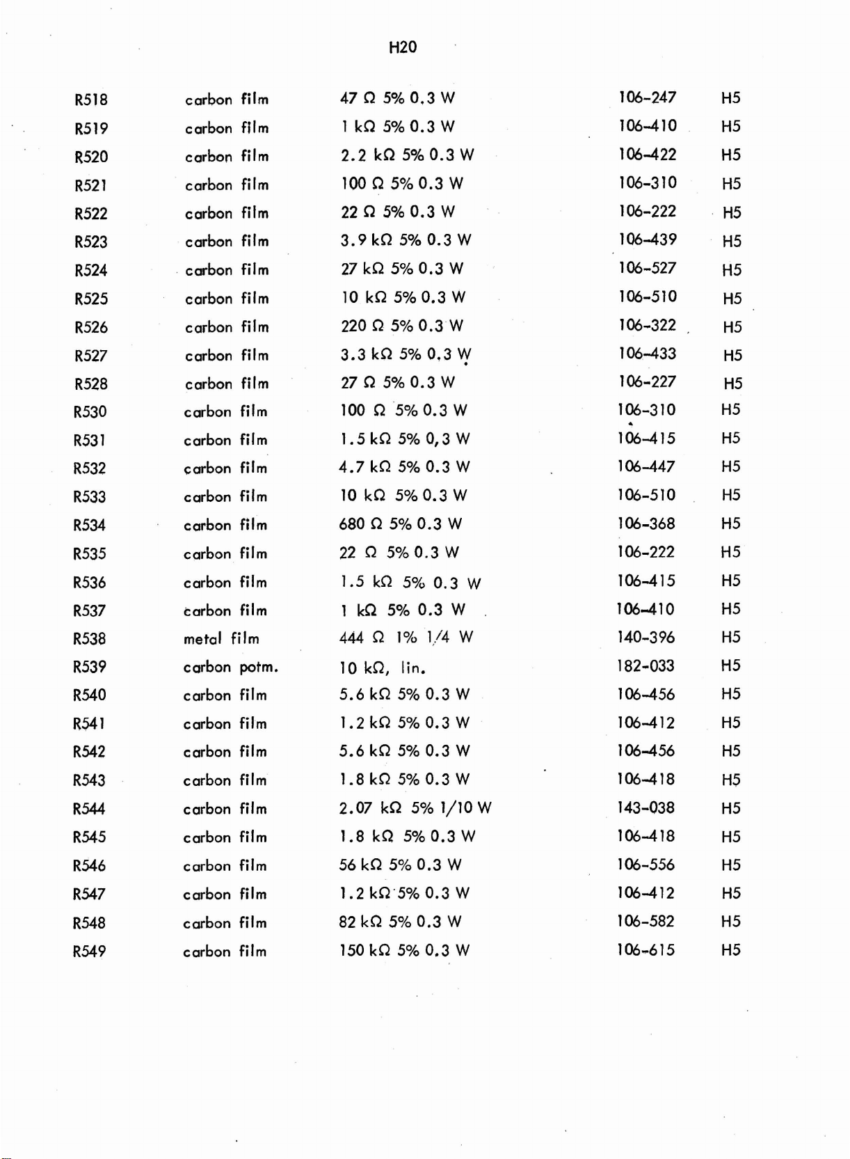
carbon
Scans by ArtekMedia © 2008
film
carbon
carbon
carbon
carbon
carbon
carbon
carbon
carbon
carbon
carbon
carbon
carbon
carbon
carbon
carbon
film
film
film
film
film
film
film
film
film
film
film
film
film
film
film
carbon
carbon
carbon
metal
carbon
carbon
carbon
carbon
carbon
carbon
carbon
carbon
carbon
carbon
carbon
film
film
film
film
potm.
film
film
film
film
film
film
film
film
film
film
10 kR,
5.6
kR
1.2
kC2
lin.
5%
5%
0.3
0.3
W
W
Page 74

carbon
Scans by ArtekMedia © 2008
carbon
carbon
carbon
carbon
carbon
film
film
film
potm,
film
film
100
3.3
12
1
kR,
1.8
8.2
kR
kn
kQ
kR
kR
5%
5%
0.3
5%
0.3'~
lin.
5%
5%0.3
0.3
0.3
W
w
W
W
carbon
carbon
carbon
metal film
carbon
metal film
metal
carbon film
metal film
Designation Type
TB501
tag strip, +pole
film
film
potm.
film
film
82 kR
TAG
STRIPS
5%
0.3
W
Code
No.
Shown
Fig.
in
Page 75

PRINT
Scans by ArtekMedia © 2008
BOARD
VI
-
LIMITER,
CAPACITORS
CODE
900-245
Designation
C608
ceramic
polystyrene
tantalum
tantalum
ceramic
ceramic
ceramic
tantalum
polystyrene
ceramic
ceramic
ceramic
Value
10
pF
Accuracy and
max.
15
voltage
V
Code
No.
Shown
Fig.
267-000 H6
in
C620
1
C62
C622
C623
C624
(2625
C626
cerpmic
ceramic
ceramic
ceramic
ceramic
ceramic
ceramic
tantal um
ceramic
tantalum
ceramic
tantalum
ceramic
22
10
470
10
47
10
22
nF
pF
pF
pF
nF
pF
nF
-20/+80%
15
V
-20/+80%
15
V
-20/+80%
15
V
40
25
30
-20/+80% 40
V
213-01
1
H6
267-000 H6
V 213-014 H6
267-00 H6
V
213-016 H6
267-000 H6
V
2 13-01
1
H6
Page 76

C627
Scans by ArtekMedia © 2008
tantalum
10
pF
C628 tantalum
C630
C63
1
Designation
CR60
1
CR602
ceramic
tantalum
Type
diode
diode
diode BAX16
diode BAX16
diode
diode
Zener diode
diode
BAVI
BAVI
BAVIO
BAVI
BAVlO
0
0
0
1
N3497
10
pF'
2.2
nF
10
pF
DIODES
Code No.
Shown in
Fig.
diode
diode
diode
Designation Type
P600
P60l terminal strip
Designation Type
terminal strip,
transistor
transistor 2N3906
transistor
BAVlO
BAVlO
BAVlO
2N3906
BC149
TERM1
10
pole
TRANSISTORS
NALS
Code
Code
No,
No.
Shown in
Fig.
Shown in
Fig.
transistor
transistor BC149
transistor
transistor 2N3906
transistor 2N3906
BC149
BC149
Page 77

transistor
Scans by ArtekMedia © 2008
2N3906
Designation
transistor
transistor
transistor
transistor
transistor
transistor BC149
transistor
transistor BC149
transistor
transistor
transistor
2N3906
2N3906
2N3906
2N3906
2N3904
T
D
100
2N3906
2N3906
2N3906
RESISTORS
Value
Code
No.,
Shown
Fig.
in
carbon
carbon film
carbon
carbon film
carbon film
carbon
carbon film
carbon film
carbon film
carbon film
carbon film
carbon
carbon film
carbon film
carbon film
film
film
film
potm.
330
R
5%
0.3
470 Q 5%0,3
330
R
5%
0.3
150
R
5%
0.3
3.9
kR
5%
0.3
1.8
kS2
5%0.3
180 R 5%0.3
18 R 5% 0.3
33
kR
5% 0.3
56
kR
5%.0,3
56
kR
5%0.3
10
kn,
lin.
8.2
kR
5%
0.3
3.3
kR
5% 0.3
27
kR
W
W
W
W
W
W
W
W
W
W
W
W
W
carbon film
carbon film
5.6
68
kR
kR
Page 78

carbon
Scans by ArtekMedia © 2008
carbon
carbon
carbon
carbon
carbon
film
film
film
film
film
film
68
10
10
kS2
1
1
kR
6.8
kR
5%
kR
5% 0.3 W
kR
5%
5% 0.3
5%
kR
5%0.3
0.3
0.3 W
0.3
W
W
W
W
carbon
carbon
carbon
carbon
carbon
carbon
carbon
carbon
carbon
carbon
carbon
carbon
carbon
carbon
carbon
potm.
film
film
film
film
film
film
film
film
potm.
film
film
film
film
film
1
kR,
lin.
560
R
5% 0.3
2.2
kR
5% 0.3
1.5
kR
5%
390
R
5%
47
R
5% 0.3
1
kR
5%
1.8
kR
5%0.3
560
D 5%
kR,
lin.
6.8
kR
5%0.3
2.2
kQ
5% 0.3
1.5
kR
5% 0.3
390 R 5%
47
R
5% 0.3
0.3
0.3
0.3
0.3
0.3
W
W
W
W
W
W
W
W
W
W
W
W
W
carbon
carbon
carbon
carbon
carbon
carbon
carbon
carbon
carbon
carbon
carbon
carbon
film
film
film
film
film
film
film
film
film
film
film
film
1
kR
5% 0.3
W
1.8kR 5%0.3W
12
kR
5% 0.3
1
kR
5%
47
R 5% 0.3 W
kR
5% 0.3 W
1
68
R
5%
10
kQ
5% 0.3
10 R 5% 0.3
0.3
0.3
W
W
W
W
W
10 R 5% 0.3.W
6.8
kR
5%
0.3
6.8
kR
5% 0.3
W
W
Page 79

carbon film
Scans by ArtekMedia © 2008
6.8
kQ
5% 0.3
W
carbon film
carbon film
carbon film
carbon film
carbon film
carbon film
carbon film
wire-wound
trimmer
wire-wound
carbon film
carbon film
carbon
carbon film
wire-wound
film
100 kR 5%
4.7
kQ
5%
0.3
0.3
W
W
1.5kR 5%0.3W
680 R 5% 0.3
1.8
kR
5% 0.3 W
27
kR
5%0.3
18 kR 5% 0.3
W
W
W
4.18 kR 1%
ZZ
kR
kR
kR
kR
10%
1%
5%
5%
5% 0.3
5%
0.3
0.3
0.3
W
W
W
W
500
2.46
6.8
100 kR
4.7
47
10 kR 0.1%
Designation
W600
wire-wound
carbon
metal film
carbon film
carbon film
carbon film
carbon
coaxial cable,
pot.
film
10
10
221
10R 5%0.3
560 R 5%0.3
22
560
CABLES
50 SI,
R196/U,
kR 0.1%
kR,
lin.
kR
1% 0.1
R 5%
R
0.3
5%
0.3
0.14
W
W
W
W
W
Code No. Shown in
Fig.
m
indicates special parts manufactured
by
Radiometer.
Page 80

PRINT
Scans by ArtekMedia © 2008
BOARD
VII
-
FM
DETECTOR, CODE
900-246
Designation
C704
C705
C706
ceramic
ceramic
ceramic
ceramic
ceramic
tantalum
tantalum
ceramic
tantalum
polystyrene
polystyrene
electrolytic
polyester
Value Accuracy and
max. voltage Fig.
39
47
47
47
10
pF
nF
nF
nF
pF
5%
-20/+80% 30 V 213-016
-20/+80% 30 V
-20/+80%
I5
V
30
V
Cade
21
21
No.
1-239
3-016
213-016
267-000
Shown in
H7
H7
H7
H7
H7
\.
i
.
!
I
4
I
I
i
polyester
C715
Designation Type
CR70
1
CR702
CR703
CWO4
CR705
CR706
polystyrene
zener diode
zener diode
diode
diode
diode
diode
BZY88C3V3
BZY88C3V6
5082-281
5082-2
5082-2
8
8
BAXl6
1
1
1
1
1
4.7
nF
DIODES
5% 63
V
'
243-021
Code
No.
H7
Shown in
Fig.
Page 81

H28
Scans by ArtekMedia © 2008
RELAYS
Designation
K700
~esi~nation
x L701
xL702,
L703
Designation
Type
gas relay
Type
choke,
choke,
choke,
47
Type
203
394
pH
pH
pH
IN
DUCT
ORS
TERMINALS
Code
Code No.
Code No. Shown in
No.
Showsl in
Fig.
Shown in
Fig.
Fig.
P700
Designation
terminal strip,
transistor
transistor
transistor
transistor
transistor
transistor
transistor
transistor
transistor
2N3W
2N3904
2N3904
2
N3904
2N3251
2N325
2N3906
BC149
TD100
21
pole
TRANSISTORS
Code No. Shown in
Fig.
1
indicates special parts manufactured
transistor
transistor
2N3906
BC149
by
Radiometer,
Page 82
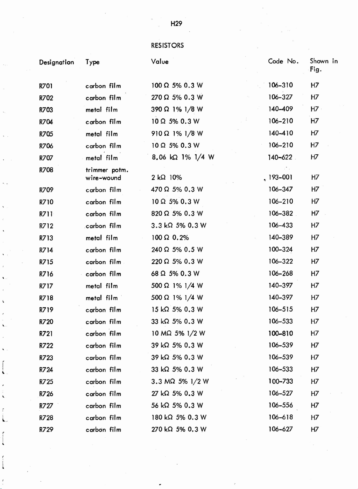
RESISTORS
Scans by ArtekMedia © 2008
Designation
W01
R702
W03
R704
R705
R706
R707
R708
R709
R710
R711
R712
Type
carbon film
carbon film
metal film
carbon film
metal film
carbon film
metal film
trimmer
wire-wound
carbon film
carbon film
carbon film
carbon film
potm.
Value
Code No.
Shawn in
Fig.
R713
R714
R715
R7 16
R717
R718
R7
19
R720
R72
R722
R723
R724
R725
R726
R727
1
metal film
carbon film
carbon film
carbon film
metal filrn
metal
carbon film
carbon film
carbon film
carbon film
carbon film
carbon film
carbon film
carbon film
carbon film
filrn
R728
R729
carbon film
carbon film
Page 83

R730
Scans by ArtekMedia © 2008
R73
1
carbon film
carbon film
82
1.8
kR
kR
5%
5%
0.3
0.3
W
W
106-582
106-418
H7
H7
R732
W33
R734
R735
R736
R737
R738
R739
R740
R74
1
Designation
W701
carbon film
carbon film
metal film
metal
metal
cermet
carbon film
cermet potm.
metal film
carbon film
Type
coaxial cable,
film
film
potm.
50
3.3
68
kR
2.25
822
7.5
1
kR
2.7
2.2
57.6
3.3
CABLES
$2,
RG196/U,
kR
kR
R
kR
kR
kR
kR,
I&,
5%
5%
1%
1%
1%
5%
0.3
0.3
1/4
1%
5%
W
l/4
W
1/4
0.3
0.3
0.10
W
1/8
W
W
W
W
W
m
106-433
106-568
140-380
140-379
1401.2
99
Code No, Shown in
H7
H7
H7
H7
H7
Fig.
Page 84

PRINT
Scans by ArtekMedia © 2008
BOARD
Vlll
-
AF
AMPLIFIER
CAPACITORS
I
+
11,
CODE
900-247
Designation Type
polystyrene
polystyrene
polystyrene
ystyene
pol
electrolytic
polystyrene
ceramic
polystyrene
ceramic
tantalum
ceramic
C812
C8
13
polystyrene
ceramic
Value Accuracy and Code No. Shown in
54.5
82
pF
nF
max.
l%63
5%
voltage Fig.
V
DIODES
Designation Type
CR80
1
CR802
CR803
Designation
I
t
(
i
x
L801
x
L802,
x
L803
indicates special parts manufactured
diode
zener diode
zener diode
Type
choke,
choke,
choke,
BAV10
400
400
400
BZY88C6V8
BZY88C6V8
INDUCTORS
pH
pH
pH
by
Radiometer.
Code No. Shown in
Fig.
Code No. Shown in
Fig.
Page 85

choke,
Scans by ArtekMedia © 2008
400
pH
choke,
Designation Type
P800
Designation Type
Q80
1
Q802
Q803
Q804
terminal strip,
transistor
transistor
transistor
transistor TDl
1
10
pH
TD121
BC149
2N3906
21
TERMINALS
20-pole
TRANSISTORS
Code
Code No. Shown in
No. Shown in
Fig.
Fig.
Q805
Q806
.
transistor
transistor
BC 149
BC149
RESISTORS
Designation Type Value
metal film
carbon film
carbon potm
carbon film
metal film
carbon film
carbon film
carbon film
.
550
i2
680 R 5% 0.3
100
3.9
MR
3.16kQ
.47
kR
22
kS2
330 R 5% 0.3
0.2%
kR,
5%
5%
lin.
5%
1%
0.3
0.3
1/8
W
W
1/2
W
1/4W
W
W
W
Code No. Shown in
Fig.
indicates special parts manufactured by Radiometer.
carbon film
carbon film
carbon film
1
1
4.7
kS2
kR
kR
5% 0.3
5%0.3
5%
0.3
W
W
W
.:
Page 86

carbon
Scans by ArtekMedia © 2008
carbon
carbon
carbon
carbon
film
film
film
film
film
180 R 5%
82
R
5%
2.2
kR
5%
560
R
5%
1
kR
5%
0.3
0.3
0.3
0.3
W
0.3
W
W
W
W
carbon
carbon
carbon
carbon
carbon
carbon
metal
carbon
metal
metal
film
film
film
film
film
film
film
film
film
strap
39kR 5%0.3
56
k8
5%
0.3
6.8
kR
5%
0.3
12
kR
5%
0.3
470 R 5%
6.8
kR
500
R
5.6
kR
12.6
ca.
0
5%
1% 1/4
5%
kR
R
0.3
0.3
0.3
0.5%
W
W
W
W
W
W
W
W
1/4
W
Page 87
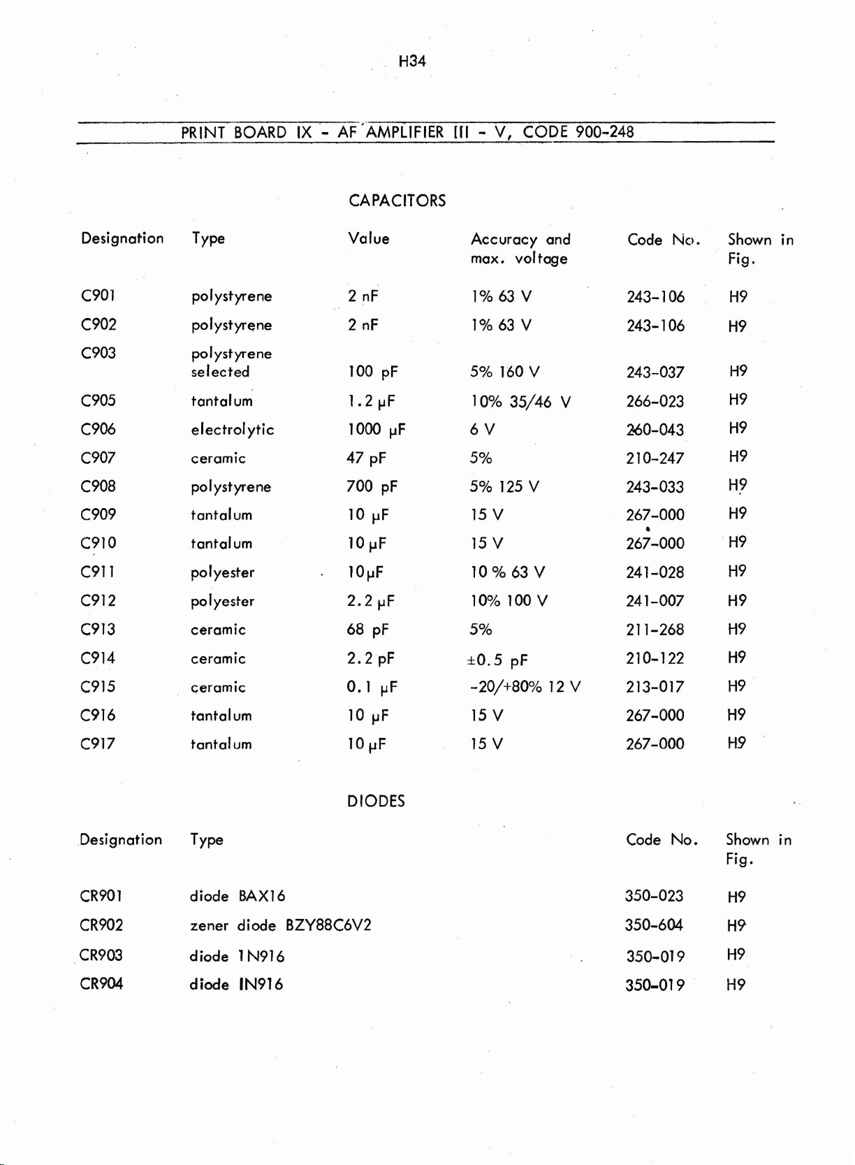
PRINT
Scans by ArtekMedia © 2008
BOARD IX
'-
AF'AMPLIFIER
CAPACITORS
Ill
-
V,
CODE
900-248
Designation Type
polystyene
polystyrene
polystyrene
selected
tantalum
electrolytic
ceramic
polystyrene
tantalum
tantalum
polyester
1
yester
po
ceramic
Value Accuracy and Code
max. voltage
No.
Shown in
Fig.
ceramic
ceramic
tantal um
tantalum
Designation Type
CR90
1
CR902
C
R903 diode 1 N916
CR90.Q
diode BAX16
zener diode BZY88C6V2
diode IN916
DIODES
Code No. Shown in
Fig.
Page 88
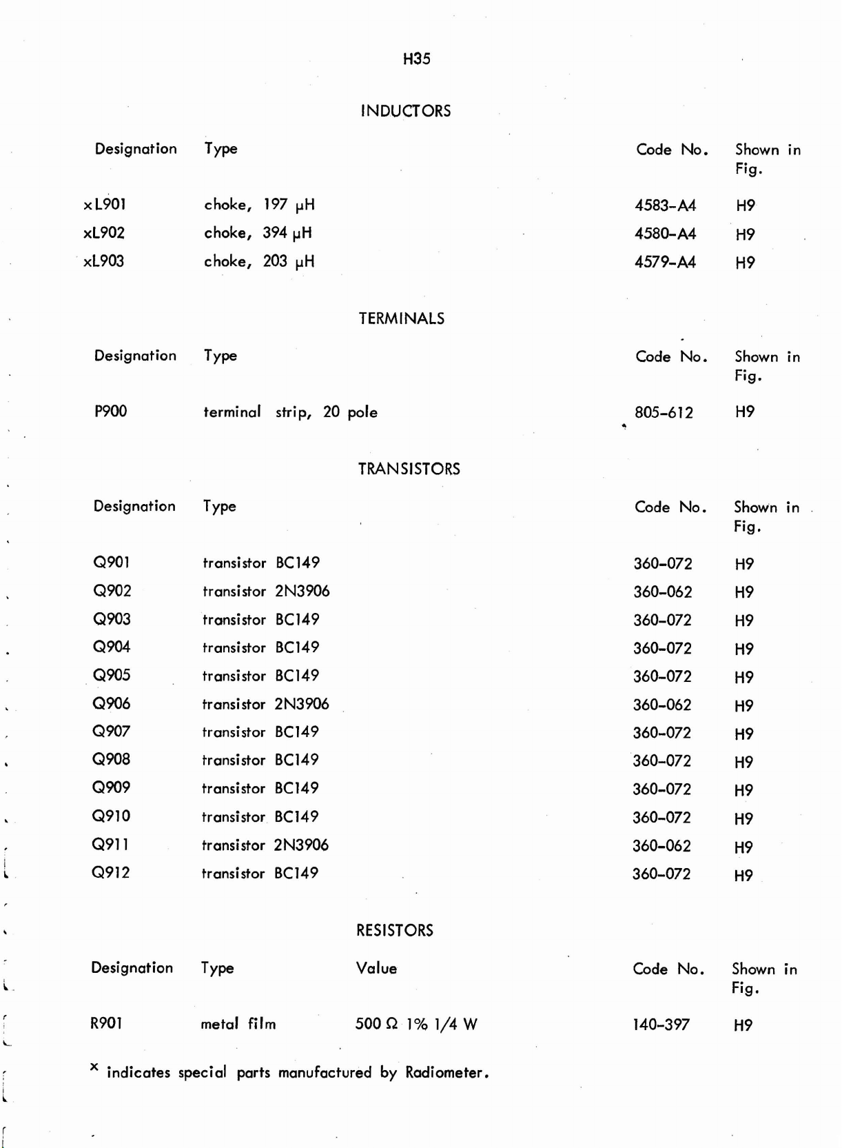
H35
Scans by ArtekMedia © 2008
INDUCTORS
Designation
x ~901 choke, 197
xL902 choke, 394
xL903 choke, 203
Designation Type
P900 terminal strip, 20
Designation Type
Type
pH
pH
pH
TERMINALS
pole
TRANSISTORS
Code No. Shown in
Fig.
Code
Code
No.
No.
Shown in
Fig.
Shown in
Fig.
transistor
transistor 2N3906
'transistor BC149
transistor BC149
transistor BC149
transistor 2N3906
transistor BC149
transistor BC149
transistor BC149
transistor, BC149
transistor 2N3906
transistor BC149
BC149
RESISTORS
Designation
R901 metal film 500
indicates special parts manufactured by Radiometer.
Type
Value
Q
1%
1/4
W
Code No.
140-397
Shown in
Fig.
Page 89

carbon film
Scans by ArtekMedia © 2008
carbon film
carbon film
carbon film
carbon film
carbon film
metal film
carbon potm.
carbon film
carbon film
carbon film
carbon film
carbon film
carbon film
carbon film
500
27
kR
S2,
5% 0.3
Iin.
W
carbon film
carbon film
metal film
metal film
metal film
carbon film
carbon potm.
metal film
carbon film,
sel ec ted
carbon film
carbon film
carbon film
carbon potm.
carbon film
10
kR,
lin.
approx.
470 kR
120 kR
5.6
0.5
5.6
5%
5%
MR
5% 1/2 W
MR,
0.3
0.3
lin.
680 R 5% 0.3
kR
W
W
W
0.3
W
carbon film
carbon film
carbon' film
carbon film
530 R
39 kR
1
kR
12
kR
5%
0.3
5%
0.3
5%0.3W
5%
0.3
W
W
W
Page 90

R935
Scans by ArtekMedia © 2008
carbon
film
1.2
kR5%
0.3
W
R936
R937
R938
carbon
metal
carbon
film
film
film
lWC2
270
kC2
100R
5%0.3
1%
1/4
5%0,3
W
W
W
Page 91

PRINT
Scans by ArtekMedia © 2008
BOARD
X
-
AF
DbTECTQR,
CAPACITORS
CODE
900-249
Designation
Designation
CRlOOl
CR1002
CR 1003
polyester
po 1 yester
polyester
polyester
ceramic
ceramic
diode
diode BAV10
diode
WVlO
I
N4002
68
nF
68
nF
0.47
pF
0.47
pF
1
nF
0.1
pF
DIODES
Accuracy
max.
voltage Fig.
and
Code No.
Code
No. Shown in
Shown
Fig.
in,
CR1004
CR
1
005
Designation Type
Pl
000
Designation Type
QlOOl
Q
1002
Q
1
003
diode I
Zener
terminal strip,
transistor
transistor
transistor
N4002
diode
2N930
2N3906
8C149
~2~86~5~6
TERMINALS
15
p~le
TRANSISTORS
.
.
Code No. Shown
Fig.
Code
No;
Shown in
Fig.
in
Page 92

H39
Scans by ArtekMedia © 2008
RESISTORS
Designation
Rl
001
R 1 002
R
1
003
R
1
004
R 1 005
R
1
006
R
1
007
R1008
R1009
RlOlO
RlOll
R1012
R1013
Type
carbon
carbon
carbon
carbon
carbon
carbon
carbon
carbon
carbon
carbon
carbon
carbon
film
potm.
film
film
film
film
film
film
film
film
film
film
metal film
Value
18MR $%@W
0.5
MS2,
5.6
MZZ
470
kQ
180 kQ
approx.
opprox,
5%
5%
5%
12
$60
Iin.
0.3
0.3
kC2
1/2
t2
W
W
W
0.3
0.3
1.2kS2 5%0.3W
120kR 5% 0.3
W
1.8kQ 5%0.3W
10
kR
5% 0,3 W
1.5
kR
5%
0.3
W
W,
W,
selected
selected
Code No.
Shown in
Fig.
R1014
R1015
R1016
metal
metal
carbon
film
film
film
Page 93

PRINT BOARD
Scans by ArtekMedia © 2008
XI
-
POWER
CAPACITORS
SUPPLY,
CODE
900-250
Designation . Type
CllOl
C1102
C1103
C1104
C1105
C1 106
C1107
C1108
C1109
ClllO
electrolytic
ceramic
ceramic
polyester
polyester
polyester
electrolytic
ceramic
polyester
polyester
Value
1000
pF
0.1
pF
15
pF
1
PF
33
nF
0.22
yF
1000
pF
33
pF
2.2
nF
0.22
pF
DIODES AND
Accura~y
max. voltage
25
V
30
V
&5%
10% 160
10%
10%
25
V
400
160
V
V
V
*5%
100h 400
10% 160
V
V
RECTIFIERS
and
Code
26 1 -029 HI
No.
Shown
Fig.
1
213-009 HI 1
210-215 HI 1
24 1 -004
240-533
24
1 -002
261 -029
HI
HI
HI
HI
1
1
1
1
2 10-233 HI 1
240-422 HI 1
24 1 -002 HI1
in
Designation
CRllOl
CR1102
CR1103
CRllOll
CR1105
CR1106
CR1107
Designation
JllOO
Type
di ode
diode
rectifier
zener diode
zener
diode
diode
I
N4002
I
N4002
B80C2000
diode
1
N4002
BAX16
Type
terminal strip,
BZY88CSV6
BZY88C6V8
TERMINALS
20
contacts
Code
3
50-409
6de
No.
No.
Shown
Fig.
HI1
Shown
Fig.
in
'
in
PI
100
terminal strip,
20
contacts
Page 94

TRANSISTORS
Scans by ArtekMedia © 2008
Designation
QllOO
QllOl
(21102
Q1103
Q1104
,
'
Q1105
Q1106
Designation
RllOl
Type
transistor
transistor
transistor
transistor
transistor
transistor
transistor
Type
cqrbon potm.
2N2905A
BC149
BC149
2N3906
2N2905A
BDY92
BDY92
with insulated mounting
with insvlated mounting
RESISTORS
Value
1
MR,
lin.
Code
No.
360-062
Code
No.
Shown in
Fig.
Hll
Shown in
Fig.
R1102
xR1103
R1104
R1105
R1106
R1107
R1108
R1109
RlllO
Rllll
R1112
R1113
R1114
R1115
R1116
carbon film
w
ire-wound
carbon film
carbon film
carbon film
carbon film
carbon film
wire-wound
carbon film
carbon film
carbon film
carbon film
carbon film
carbon potm.
carbon film
1
MR
6.8
12
68
2.7
82
2.7
2
1.2
150
2.7
5.6
2.2
1
kR,
2.7
$2
R
Q
n
5%
$2
5% 2.5
5%
5%
kS2
5%
kR
2%
kR
Q
5%
kn
kQ
kR
lin.
kR
0.3
0.3
W
0.3
W
5%
0.3
0.3
W
5% 0.3
112
w
5% 0.3
0.3
5%
0.3
5%
0.3
5% 0.3
5% 0.3
W
W
W
W
W
W
W
W
W
W
X
indicates special parts manufactured
by
Radiometer.
Page 95

carbon film
Scans by ArtekMedia © 2008
1.2
kQ
5% 1/2
W
Designation
W1101
carbon
wire-wound
carbon film
carbon
carbon film
carbon film
carbon
metal film
metal film
carbon film
carbon film
Type
power line with plug,
film
potm.
film
1.2kR 5%0.3 W
8.2
R
5%
2.5
W
330
Q
5%
0.3
W
1
MR, lin.
2.7
MR
5%
1/2
loon
4.7
4.4
4.4
2.2
4.7 kR
5% 0.3
kR
5%
0.3
kS2
0.5% 1/4 W
kR
0.5% 1/4
kS2
5%
0.3
5%
0.3
w
W
W
W
CABLES
1.7
rn
W
W
Code
6
15-005
No.
Shown
Fig.
HI
1
in
W1102
Designutlon
Tll
01 transformer
shielded cable,
Type
0.5
TBS593
m
TRANSFORMER
Code
No.
770-593
X
indicates special parts manufactured by Radiometer.
Page 96

CAPACITORS
Scans by ArtekMedia © 2008
Designation
Type
trimmer
trimmer
trimmer
tr
i
mmer
ceramic
ceramic
ceramic
ceramic
ceramic
ceramic
ceramic
ceramic
Val we
Code
No.
I
I
k.
i
Designation
xL1201
L
1202 ferrite
L1203 ferrite
L1204
Type
coil
ferrite
tube,
tube,
tube, 7
15
15 mm
mm
INDUCTORS
mm
Code
No.
Shown in
Fig.
i
i
X
indicates special parts mgrlufactured
by
Radiometer.
Page 97

TERMINALS
Scans by ArtekMedia © 2008
Designation
.
PI200
Designation
Q1201 transistor BF173
Q1202 transistor BFW30
Q1203 transistor BFW30
Type
terminal strip, 13
Type
pole
TRANSISTORS
RESISTORS
Code
805-639
No.
H
12
We
360-095 ~12
No.
Shown
Fig.
in
Designation
Designation
Type
carbon film
carbon film
carbon film
carbon film
carbon
carbon film
carbon film
carbon film
cermet potm,
film
Type
Value
SWITCHES
We
No.
Code
Shown in
Fig.
No. Shown in
Fig.
$1201 switch
"CHANNEL"
Page 98

H45
Scans by ArtekMedia © 2008
CABLES.
Designation
Wl201
Designation
Type
coaxial
Type
crystal holder
x
.pointer knob
cable,
1
10
(HC
R
MISCELLANEOUS
25/lJ)
6de
Code
8
1
6-201
No.
No.
852-1 1 1
indicates
special
parts manufactured
by
Radiometer.
Page 99

MODIFICATIONS FOR MODULATION
Scans by ArtekMedia © 2008
The
coa~ial bushing J1, code 800-108, of the Modulation Meter, type AFM2,
METER,
TYPE
AFM2$3
is
re-
placed
by
the coaxial bushing J1, code 800-203,
in
the Modulqtion Meter, type
AFM2S3.
.
,-
--
-
--
MODIFICATIONS FOR MODULATION
-
.-
.
---
--
-
METER.
---
TYPE AFM255
The following components are removed from the regular Modulation Meter, type AFM2,
and replaced
Designation Type
as
follows in the Modulation Meter, type AFM2S5.
Value
polystyrene
carbon film
carbon film
700
pF
330 R
1 kQ
5%
5%
0.3
0.3
W
W
Code No.
Shown
Fig.
H9
in
metal film
metal film
metal
film
corbon potm.
corbon potm.
metal film
Designation Type
C908 polystyrene
C918 ceramic
R912 carbon film
R917 carbon film
R919 metal film
R920 metal film
36.1
kR
1%
850 n 1% 114
2.04
kSZ
1%
1/4
10
kQ, lin.
kR,
10
50 kR
lin.
1%
114
Value
pF 5% 125 V
150
0.5
pF
5%
1.2 kR 5% 0.3
680 R 0.5
75
kQ 1% 0.2
600 R
1%
W
0.2
1/4
w
W
5%
W
W
W
W
Code No.
W
R923 carbon potm.
R924 metal film
R939 carbon film
25 kR
100
kR
kQ
330
lin.
1%
5%
0.2
W
'
Page 100

MODIFICATIONS FOR MODULATION
Scans by ArtekMedia © 2008
METER.
TYPE
AFM2S6
The following components are removed from the
and replaced
Designation
C317
R320
Designation
C317
R320
as
follows in
Type
ceramic
carbon film
Type
ceramic
carbon film
the
Modulalion Meter,
(APM?)
Va
Iue
10
pF
150
R
Value
22
pF
56
R
5%
5%
5%
5%
0.2
regular
type
0.3
W
W
Modulotion Meter,
AFM2S6.
Code
21
Code
21
type
AFM2,
NO.
0-21
0
No,
1
-222 H3
Shown
Fig.
H3
in
 Loading...