

QUICK LOGIC QL5232-33APB456I, QL5232-33APB456M, QL5232-33APQ208C, QL5232-33APQ208I, QL5232-33APQ208M Datasheet
...
Rev B
33 MHz/32-bit PCI Master/Target with Embedded Programmable Logic and dual Port SRAM
QL5232 - QuickPCI
TM
last updated 12/3/99
Device Highlights
High Performance PCI Controller
■ 32-bit / 33 MHz PCI Master/Target
■ Zero-wait state PCI Master provides 132 MB/s transfer rates
■ Programmable back-end interface to optional local processor
■ Independent PCI bus (33 MHz) and local bus
(up to 160 MHz) clocks
■ Fully customizable PCI Configuration Space
■ Configurable FIFOs with depths up to 256
■ Reference design with driver code (Win 95/98/Win 2000/
NT4.0) available
■ PCI v2.2 compliant
■ Supports Type 0 Configuration Cycles in Target mode
■ 3.3V, 5V Tolerant PCI signaling supports Universal
PCI Adapter designs
■ 3.3V CMOS in 208-pin PQFP and 456-pin PBGA
■ Supports endian conversions
■ Unlimited/Continuous Burst Transfers Supported
Extendable PCI Functionality
■ Support for Configuration Space from 0x40 to 0x3FF
■ Multi-Function, Expanded Capabilities, & Expansion ROM
capable
■ Power management, Compact PCI, hot-swap/hot-plug
compatible
■ PCI v2.2 Power Management Spec compatible
■ PCI v2.2 Vital Product Data (VPD) configuration support
■ Programmable Interrupt Generator
■ I
2
O support with local processor
■ Mailbox register support
Programmable Logic
■ 122K system gates / 1302 Logic Cells
■ 25,344 RAM bits, up to 266 I/O pins
■ 250 MHz 16-bit counters, 275 MHz Datapaths, 160 MHz FIFOs
■ All back-end interface and glue-logic can be implemented on chip
■ 11 64-deep FIFOs or 5 128-deep FIFOs or a 2 256-deep FIFO
or a combination that requires 22 or less QuickLogic RAM
Modules
■ (3) 32-bit busses interface between the PCI Controller and the
Programmable Logic
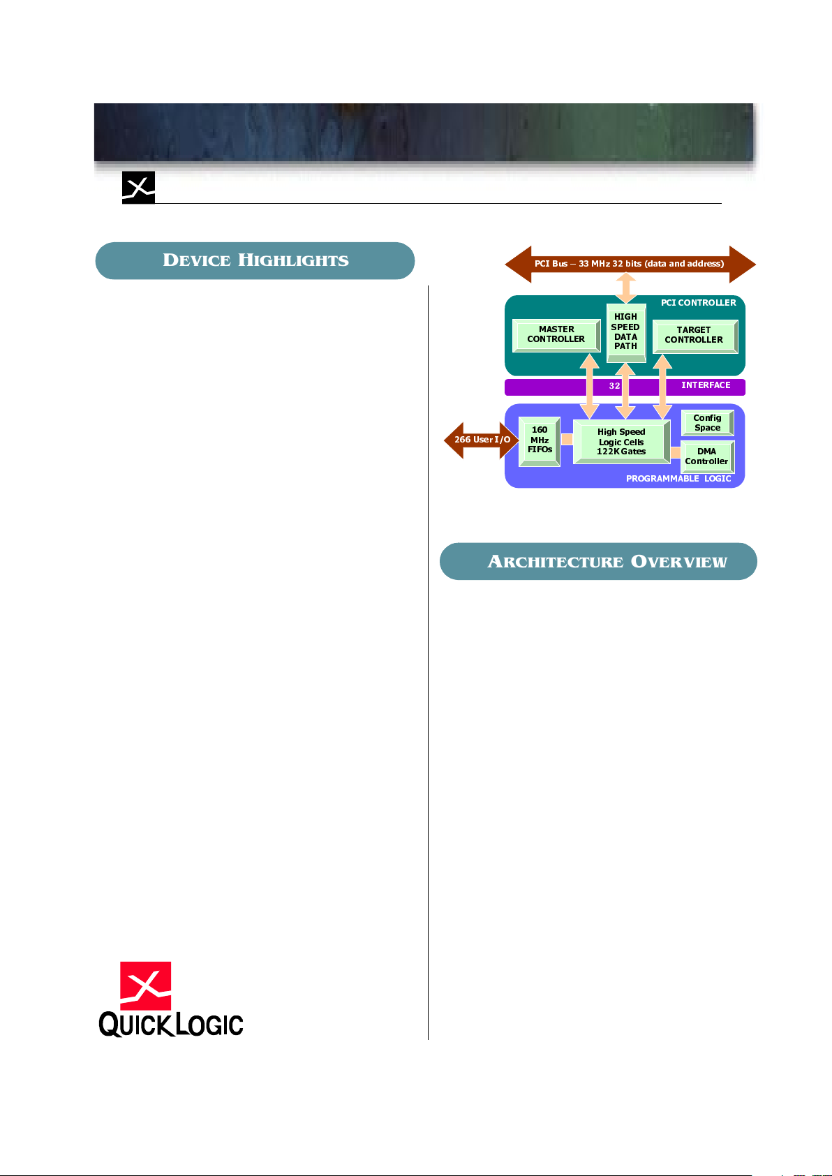
FIGURE 1. QL5232 Diagram
Architecture Overview
The QL5232 device in the QuickLogic QuickPCI ESP
(Embedded Standard Product) family provides a
complete and customizable PCI interface solution
combined with 122,000 system gates of
programmable logic. This device eliminates any need
for the designer to worry about PCI bus compliance,
yet allows for the maximum 32-bit PCI bus bandwidth
(132 MB/s).
The programmable logic portion of the device
contains 1302 QuickLogic Logic Cells, and 22
QuickLogic Dual-Port RAM Blocks. These
configurable RAM blocks can be configured in many
width/depth combinations. They can also be
combined with logic cells to form FIFOs, or be
initialized via Serial EEPROM on power-up and used
as ROMs.
The QL5232 device meets PCI 2.2 electrical and
timing specifications and has been fully hardwaretested. This device also supports the Win’98 and
PC’98 standards. The QL5232 device features 3.3volt operation with multi-volt compatible I/Os. Thus it
can easily operate in 3-volt systems and is fully
compatible with 3.3V,5V or Universal PCI card
development.
&RQILJ
6SDFH
0+]
),)2V
0$67(5
&21752//(5
,17(5)$&(
352*5$00$%/(
/2*,&
32
3&,%XV±0+]ELWVGDWDDQGDGGUHVV
8VHU,2
3&,&21752//(5
'0$
&RQWUROOHU
+,*+
63(('
'$7$
3$7+
+LJK6SHHG
/RJLF&HOOV
.*DWHV
7$5*(7
&21752//(5
D
EVICE HIGHLIGHTS
A
RCHITECTURE OVERVIEW
2 Preliminary
QL5232 - QuickPCI
TM
2
Rev B
PCI Controller
The PCI Controller is a 32-bit/33 MHz PCI 2.2
Compliant Master/Target Controller. It is capable of
infinite length Master Write and Read transactions at
zero wait state (132 MBytes/second). The Master
will never insert wait states during transfers, so data
should be supplied or received by FIFOs, which can
be configured in the programmable region of the
device. The Master Controller will most often be
operated by a DMA Controller in the programmable
region of the device. A DMA Controller reference
design is available. The Target interface offers full
PCI Configuration Space and flexible target addressing. Any number of 32-bit BARs may be configured,
as either memory or I/O space. All required and
options PCI 2.2 Configuration Space registers can be
implemented within the programmable region of the
device. A reference design of a Target Configuration
and Addressing module is provided.
The interface ports are divided into a set of ports for
master transactions and a set for target transactions.
The Master DMA controller and Target Configuration Space and Address Decoding are done in the
programmable logic region of the device. Since
these functions are not timing critical, leaving these
elements in the programmable region allows the
greatest degree of flexibility to the designer. Reference DMA controller, Configuration Space, and
Address Decoding blocks are included so that the
design cycle can be minimized.
Configuration Space and Address
Decode
The configuration space is completely customizable
in the programmable region of the device. PCI
address and command decoding is performed by
logic in the programmable section of the device. This
allows support for any size of memory or I/O space
for back-end logic. It also allows the user to implement any subset of the PCI commands supported by
the QL5232. QuickLogic provides a reference
Address Register/Counter and Command Decode
block.
DMA Master/Target Control
The customizable DMA controller included with the
QuickWorks design software contains the following
features:
■ Configurable DMA count size for reads and writes
(up to 30-bits)
■ Configurable DMA burst size for PCI (including
unlimited/continuous burst)
■ Programmable Arbitration between DMA Read &
Write transactions
■ DMA Registers may be mapped to any area of
Target Memory Space
- Read Address (32-bit register)
- Write Address (32-bit register)
- Read Length (16-bit register) / Write Length
(16-bit register)
- Control and Status (32-bit register, includes 8 bit
Burst Length)
■ DMA Registers are available to the local design or
the PCI bus
■ Programmable Interrupt Control to signal end of
transfer or other event
Configurable FIFOs
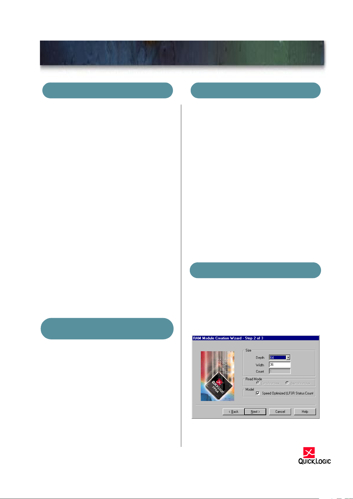
FIFOs may be created with the Ram/FIFO wizard in
the QuickWorks tools. The figure below shows the
graphical interface used to create these FIFOs.
FIFOs may be designed up to 256 deep. With 22
RAM cells available in the QL5232, that allows for
up to 11 FIFOs at 64 deep (36 wide), 5 FIFOs at 128
deep (36 wide), or 2 FIFOs at 256 deep (36 wide).
FIGURE 2. Graphical Interface to create FIFO
PCI C
ONTROLLER
C
ONFIGURATION SPACE
AND
A
DDRESS DECODE
DMA MASTER/TARGET CONTROL
C
ONFIGURABLE
FIFO
S
3
Rev B
QL5232 - QuickPCI
TM
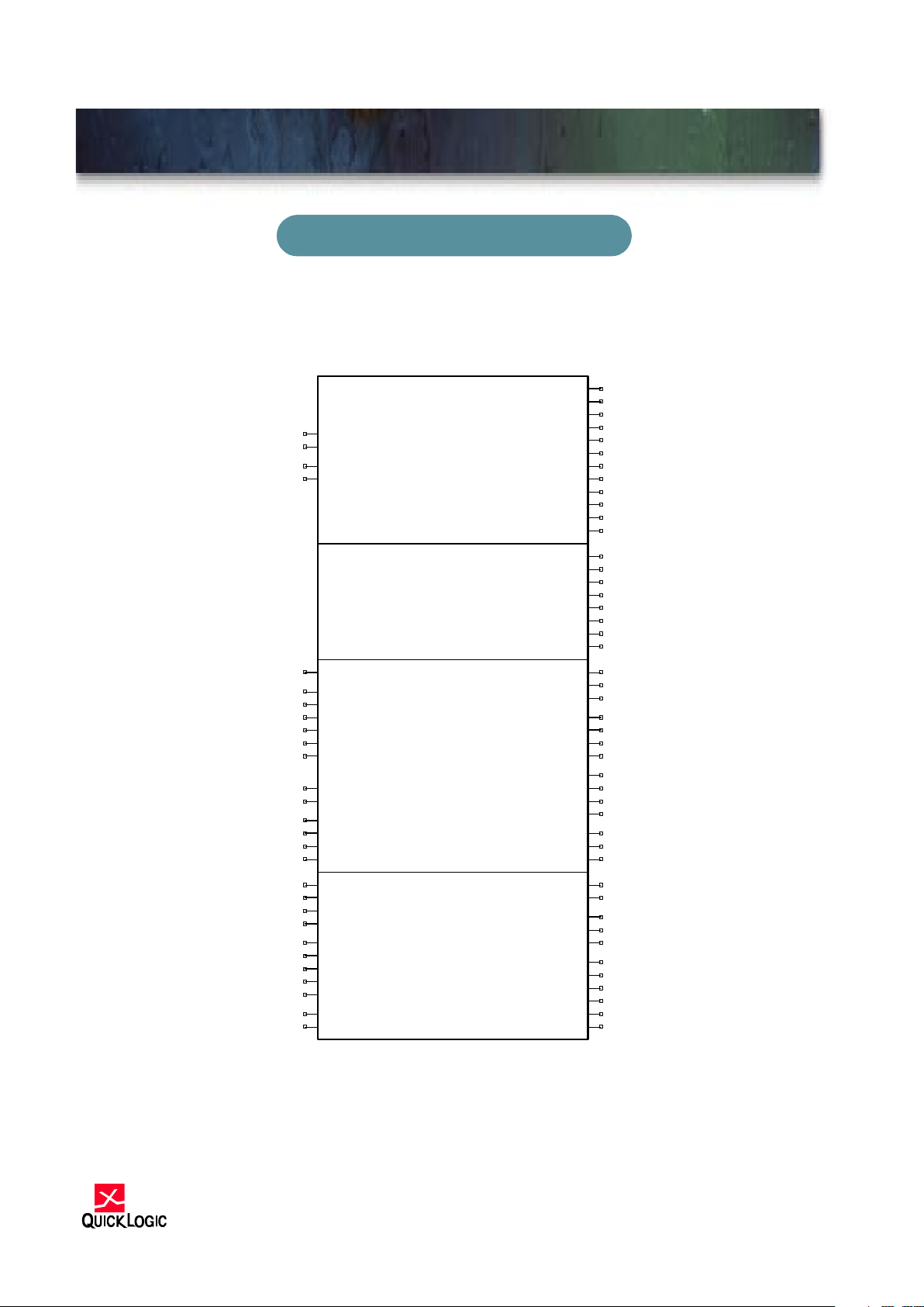
PCI Interface Symbol
The figure below shows the interface symbol you would use in your schematic design in order to attach the local
interface programmable logic design to the PCI core. If you were designing with a top-level Verilog or VHDL file,
then you would use a structural instantiation of this PCI32 block, instead of a graphical symbol.
FIGURE 3. PCI Interface Symbol
Master
Target
PCI Pads
PCI Signals
PCI32
Cfg_CmdReg6
Cfg_CmdReg8
Cfg_LatCnt[7:0]
Cfg_RdData[31:0]
CLK
GNTN
IDSEL
Mst_Burst_Req
Mst_LatCntEn
Mst_One_Read
Mst_RdAd[31:0]
Mst_RdCmd[1:0]
Mst_RdMode
Mst_Two_Reads
Mst_WrAd[31:0]
Mst_WrData[31:0]
Mst_WrData_Valid
Mst_WrMode
RSTN
Usr_Interrupt
Usr_MstRdAd_Sel
Usr_MstWrAd_Sel
Usr_RdData[31:0]
Usr_RdDecode
Usr_Rdy
Usr_Select
Usr_Stop
Usr_WrDecode
AD[31:0]
CBEN[3:0]
DEVSELN
FRAMEN
IRDYN
PAR
PERRN
STOPN
TRDYN
Cfg_MstPERR_Det
Cfg_PERR_Det
Cfg_SERR_Sig
Cfg_Write
INTAN
Mst_IRDYN
Mst_Last_Cycle
Mst_RdBurst_Done
Mst_RdData[31:0]
Mst_RdData_Valid
Mst_REQN
Mst_Tabort_Det
Mst_TTO_Det
Mst_WrBurst_Done
Mst_WrData_Rdy
Mst_Xfer_D1
PCI_clock
PCI_DEVSELN_D1
PCI_FRAMEN_D1
PCI_IDSEL_D1
PCI_IRDYN_D1
PCI_reset
PCI_STOPN_D1
PCI_TRDYN_D1
REQN
SERRN
Usr_Addr_WrData[31:0]
Usr_Adr_Inc
Usr_Adr_Valid
Usr_CBE[3:0]
Usr_Devsel
Usr_Last_Cycle_D1
Usr_STOPN
Usr_TRDYN
Usr_Write
Usr_WrReq
PCI Interface Symbol

4 Preliminary
QL5232 - QuickPCI
TM
4
Rev B
PCI Master Interface
The internal signals used to interface with the PCI controller in the QL5232 are listed below, along with a
description of each signal. The direction of the signal indicates if it is an input provided by the local interface (i) or
an output provided by the PCI controller (o). Signals that end with the character ‘N’ should be considered activelow (for example, Mst_IRDYN
Mst_WrAd[31:0] I Address for master DMA writes. This address must be treated as valid from the
beginning of a DMA burst write until the DMA write operation is complete. It must
be incremented (by 4) each time data is transferred on the PCI bus, since only
DWORD (4 byte) transfers are supported.
Mst_RdAd[31:0] I Address for master DMA reads. This address must be treated as valid from the
beginning of a DMA burst read until the DMA read operation is complete. It must be
incremented (by 4) each time data is transferred on the PCI bus, since only DWORD
(4 byte) transfers are supported.
Mst_WrMode I DMA state machine in “write” mod e. This must be asserted at the beginning of a
Master Transfer, and must be held until th e Master Transfer completed
(Mst_WrBurst_Done).
Mst_RdMode I DMA state machine in “read” mode. This must be asserted at the beginning of a
Master Transfer, and must be held until th e Master Transfer completed
(Mst_RdBurst_Done).
Mst_Burst_Req I Request use of the PCI bus. This signal should be held from when the DMA
controller is ready to provide the first data, until the transfer is complete
(Mst_WrBurst Done or Mst_RdBurst_Done).
Mst_One_Read I This signals to the PCI core that one data transfer remains in the burst. This signal
must be asserted when only one DWORD remains to be transferred on the PCI bus.
Mst_Two_Reads I Two or less data transfers remain in the burst. This signal must be asserted when two
or less DWORDs remain to be transferred on the PCI bus.
Mst_WrData[31:0] I Data for master DMA writes (to PCI bus).
Mst_WrData_Valid I Data valid on Mst_WrData[31:0].
Mst_WrData_Rdy O Data receive acknowledge for Mst_WrData[31:0]. This serves as a POP control for a
FIFO which provides data to the PCI core.
Mst_WrBurst_Done O Master write pipeline is empty, which indicates that the Write burst transaction is
completed.
Mst_RdData[31:0] O Data for master DMA reads (from PCI bus).
Mst_RdData_Valid O Data valid on Mst_RdData[31:0]. This serves as a PUSH control for a F I FO that
receives data from the PCI core.
Mst_RdBurst_Done O Master read pipeline is empty, which indicates that Read burst transaction is
completed.
Mst_RdCmd[1:0] I Type of PCI read command to be used for DMA reads:
00 or 01 = Memory Read
10 = Memory Read Line
11 = Memory Read Multiple
Mst_LatCntEn I Enable Latency Counter. Set to 0 to ignore the Latency Timer in the PCI configuration
space (offset 0Ch). For full PCI complian ce, this port should be always set to 1.
Mst_Xfer_D1 O Data was transferred on the previous PCI clock. Useful for updating DMA transfer
counts on DMA Read operations.
Mst_Last_Cycle O Active during the last data transfer of a PCI master transaction.
Mst_REQN O The PCI REQN signal generated by this device as PCI master. Not usually used in the
back-end design.
Mst_IRDYN O The PCI IRDYN signal generated by this device as PCI master. Not usually used in
the back-end design.
Mst_Tabort_Det O Target abort detected during master transaction. This is normally an error condition to
be handled in the DMA controller.
Mst_TTO_Det O Target timeout detected (no response from target). This is normally an error condition
to be handled in the DMA controller.
PCI Master Interface

5
Rev B
QL5232 - QuickPCI
TM
PCI Target Interface
Usr_Addr_WrData[31:0] O Target address and data from target writes. During all target
accesses, the address will be presented on
Usr_Addr_WrData[31:0] and simultaneously, Usr_Adr_Valid will
be active. During target write transactions, this po r t will present
write data to the PCI configuration space or user logic.
Usr_CBE[3:0] O PCI command and byte enables. During target accesses, the PCI
command will be presented on Usr_CBE[3:0] and simultaneously,
Usr_Adr_Valid will be active. During target read or write
transactions, this port will present acti ve-low byte-enables to the
PCI configuration space or user logic.
Usr_Adr_Valid O Indicates the beginning of a PCI transaction, and that a target
address is valid on Usr_Addr_WrData[31:0] and the PCI
command is valid on Usr_CBE[3:0]. When this signal is active,
the target address must be latched and decoded to determine if this
address belongs to the device’s memory space. Also, the PCI
command must be decoded to determine the type of PCI
transaction. On subsequent clocks of a target access, this signal
will be low, indicating that data (not an address) is present on
Usr_Addr_WrData[31:0].
Usr_Adr_Inc O Indicates that the target address should be incremented, because
the previous data transfer has completed. During burst target
accesses, the target address is only presented to the back-end logic
at the beginning of the transaction (when Usr_Adr_Valid is
active), and must therefore be latched and incremented (by 4) for
subsequent data transfers.
Usr_WrReq O This signal will be active for the duration of a target write
transaction, and may be used by back-end logic to turn on outputenables for transmitting the data off-chip.
Usr_RdDecode I Active when a “user read” command has been decoded from the
Usr_CBE[3:0] bus. This command may be mapped from any of
the PCI “read” commands, such as Memory Read, Memory Read
Line, Memory Read Multiple, I/O Read, etc.
Usr_WrDecode I Active when a “user write” command has been decoded from the
Usr_CBE[3:0] bus. This command may be mapped from any of
the PCI “write” commands, such as Memory Write or I/O Write.
Usr_Select I The address on Usr_Addr_WrData[31:0] has been decoded and
determined to be within the address space of the device.
Usr_Addr_WrData[31:0] must be compared to each of the valid
Base Address Registers in the PCI configuration space. Also, this
signal must be gated by the Memory Access Enable or I/O Access
Enable registers in the PCI configuration space (Command
Register bits 1 or 0 at offset 04h).
Usr_Write O Write enable for data on Usr_Addr_WrData[31:0] during PCI
writes.
Cfg_Write O Write enable for data on Usr_Addr_WrData[31:0] during PCI
configuration write transactions.
Cfg_RdData[31:0] I Data from the PCI configuration registers, required to be presented
during PCI configuration read s.
Usr_RdData[31:0] I Data from the back-end user logic (and/or DMA configuration
registers), required to be presented during PCI reads.
PCI Target Interface
6 Preliminary
QL5232 - QuickPCI
TM
6
Rev B
PCI Target Interface (Continued)
Cfg_RdData[31:0] I Data from the PCI configuration registers, required to be presented during PCI
configuration reads.
Usr_RdData[31:0] I Data from the back-end user logic (and/or DMA configuration registers),
required to be presented during PCI reads.
Cfg_CmdReg8
Cfg_CmdReg6
I Bits 6 and 8 from the Command Register in the PCI configuration space (offset
04h).
Cfg_LatCnt[7:0] I 8-bit value of the Latency Timer in the PCI configuration space (offset 0Ch).
Usr_MstRdAd_Sel I Used when a target read operation should return the value set on the
Mst_RdAd[31:0] pins. This select pin saves on logic which would otherwise
need to be used to multiplex Mst_Rd Ad[31:0] into the Usr_RdData[31:0] bus.
When this signal is asserted, the data on Usr_RdData[31:0] is ignored.
Usr_MstWrAd_Sel I Used when a target read operation should return the value set on the
Mst_WrAd[31:0] pins. This select pin saves on logic which would otherwise
need to be used to multiplex Mst_WrAd[31 :0] into the Usr_RdData[31:0] bus.
When this signal is asserted, the data on Usr_RdData[31:0] is ignored.
Cfg_PERR_Det O Parity error detected on the PCI bus. When this signal is active, bit 15 of the
Status Register must be set in the PCI configuration space (offset 04h).
Cfg_SERR_Sig O System error asserted on the PCI bus. When this signal is active, the Signalled
System Error bit, bit 14 of the Status Register, must be set in t he PCI
configuration space (offset 04h).
Cfg_MstPERR_Det O Data parity error detected on the PCI bus by the master. When this signal is
active, bit 8 of the Status Register must be set in the PCI configuration space
(offset 04h).
Usr_TRDYN O Copy of the TRDYN signal as driven by the PCI target interface.
Usr_STOPN O Copy of the STOPN signal as driven by the PCI target interface.
Usr_Devsel O Inverted copy of the DEVSELN signal as driven by the PCI target interface.
Usr_Last_Cycle_D1 O Last transfer in a PCI transaction is occurring.
Usr_Rdy I Used to delay (add wait states to) a PCI transaction when the back end needs
additional time. Subject to PCI latency restrictions.
Usr_Stop I Used to prematurely stop a PCI target access on the next PCI clock.
Usr_Interrupt I Used to signal an interrupt on the PCI bus.

7
Rev B
QL5232 - QuickPCI
TM
PCI Internal Signals
RAM Module Features
The QL5232 device has twenty-two 1,152-bit RAM
modules, for a total of 25,344 RAM bits. Using two
“mode” pins, designers can configure each module
into 64 (deep) x18 (wide), 128x9, 256x4, or 512x2
blocks. See the figure below. The blocks are also
easily cascadable to increase their effective width or
depth.
The RAM modules are “dual-ported”, with
completely independent READ and WRITE ports and
separate READ and WRITE clocks. The READ ports
support asynchronous and synchronous operation,
while the WRITE ports support synchronous
operation. Each port has 18 data lines and 9 address
lines, allowing word lengths of up to 18 bits and
address spaces of up to 512 words. Depending on
the mode selected, however, some higher order data
or address lines may not be used.
The Write Enable (WE) line acts as a clock enable for
synchronous write operation. The Read Enable (RE)
acts as a clock enable for synchronous READ
operation (ASYNCRD input low), or as a flowthrough enable for asynchronous READ operation
(ASYNCRD input high).
Designers can cascade multiple RAM modules to
increase the depth or width allowed in single modules
by connecting corresponding address lines together
and dividing the words between modules. This
approach allows up to 512-deep configurations as
large as 28 bits wide in the QL5232 device.
A similar technique can be used to create depths
greater than 512 words. In this case address signals
higher than the eighth bit are encoded onto the write
enable (WE) input for WRITE operations. The READ
data outputs are multiplexed together using encoded
higher READ address bits for the multiplexer
SELECT signals.
FIGURE 4. RAM Module
PCI_clock O PCI clock.
PCI_reset O PCI reset signal.
PCI_IRDYN_D1 O Copy of the IRDYN signal from the PCI bus, delayed by one clock.
PCI_FRAMEN_D1 O Copy of the FRAMEN signal from the PCI bus, delayed by one clock.
PCI_DEVSELN_D1 O Copy of the DEVSELN signal from the PCI bus, delayed by one clock.
PCI_TRDYN_D1 O Copy of the TRDYN signal from the PCI bus, delayed by one clock.
PCI_STOPN_D1 O Copy of the STOPN signal from the PCI bus, delayed by one clock.
PCI_IDSEL_D1 O Copy of the IDSEL signal from the PCI bus, delayed by one clock.
MODE[1:0]
WA[a:0]
WD[w:0]
WE
WCLK
RAM Module
ASYNCRD
RA[a:0]
RD[w:0]
RE
RCLK
Address
Buses [a:0]
Data Buses
[w:0]
64x18
[5:0] [17:0]
128x9
[6:0] [8:0]
256x4
[7:0]
>@
512x2
[8:0] [1:0]
PCI Internal Signals
RAM Module Features

8 Preliminary
QL5232 - QuickPCI
TM
8
Rev B
JTAG Support
JTAG pins support IEEE standard 1149.1a to provide boundary scan capability for the QL5232
device. Six pins are dedicated to JTAG and programming functions on each QL5232 device, and are
unavailable for general design input and output signals. TDI, TDO, TCK, TMS, and TRSTB are JTAG
pins. A sixth pin, STM, is used only for programming.
Development Tool Support
Software support for the QL5232 device is available
through the QuickWorks
development package.
This turnkey PC-based QuickWorks
package,
shown in Figure 5, provides a complete ESP software
solution with design entry, logic synthesis, place and
route, and simulation. QuickWorks
includes
VHDL, Verilog, schematic, and mixed-mode entry
with fast and efficient logic synthesis provided by the
integrated Synplicity Synplify Lite tool, specially
tuned to take advantage of the QL5232 architecture.
QuickWorks
also provides functional and timing
simulation for guaranteed timing and source-level
debugging.
The UNIX-based QuickTool s and PC-based Quick-
Works- Lite packages are a subset of QuickWorks
and provide a solution for designers who use schematic-only design flow third-party tools for design
entry, synthesis, or simulation. QuickTools and
QuickWorks-Lite read EDIF netlists and provide
support for all QuickLogic devices. QuickTool s
and QuickWorks-Lite also support a wide range of
third-party modeling and simulation tools. In addition,
the PC-based package combines all the features of
QuickWorks-Lite with the SCS schematic capture
environment, providing a low-cost design entry and
compilation solution.
FIGURE 5. QuickWorks Tool Suite
Schematic
Schematic
Turbo
HDL Editor
Third Party
Design
Entry
& Synthesis
Third Party
Simulation
VHDL/
VHDL/
Verilog
Verilog
SCS
Tools
Silos III
Simulator
QuickTool/QuicChi:
Optimize, Place,
Route
Mixed-Mode Design
Mixed-Mode Design
Synplify-
HDL
Synthesi
Quick
Works
Design Software
VeriBest
JTAG Support
Development Tool Support

9
Rev B
QL5232 - QuickPCI
TM
Pin Type Descriptions
The QL5232 Device Pins are indicated in the table below. These are pins on the device, some of which connect
to the PCI bus, and others that are programmable as user IO.
* See QuickNote 65 on the QuickLogic web site for
information on RAM initialization.
Type Description
IN Input. A standard input-only
signal
OUT Totem pole output. A standard
active output driver
T/S Tri-state. A bi-directional, tri-state
input/output pin
S/T/S Sustained Tri-state. An active low
tri-state signal driven by one PCI
agent at a time. It must be driven
high for at least one clock before
being disabled (set to Hi-Z). A
pull-up needs to be provided by
the PCI system central resource to
sustain the inactive state once the
active driver has released the
signal.
O/D Open Drain. Allows multiple
devices to share this pin as a
wired-or.
Pin/Bus
Name
Type Function
VCC IN Supply pin. Tie to 3.3V supply.
VCCIO IN Supply pin for I/O. Set to 3.3V
for 3.3V I/O, 5V for 5.0V compliant I/O
GND IN Ground pin. Tie to GND on the
PCB.
I/O T/S Programmable Input/Output/Tri-
State/Bi-directional Pin.
GLCK/I IN Programmable Global Network or
Input-only pin. Tie to VCC or
GND if unused.
ACLK/I IN Programmable Array Network or
Input-only pin. Tie to VCC or
GND if unused.
RSVRD IN Reserved by QuickLogic for future
PCB.
TDI/RSI* IN JTAG Data In/RAM Init. Serial
Data In. Tie to VCC if unused.
Connect to Serial EPROM data
for RAM init.
TDO/
RCO*
OUT JTAG Data Out/RAM Init Clock.
Leave unconnected if unused.
Connect to Serial EPROM clock
for RAM init.
TCK IN JTAG Clock. Tie to GND if
unused.
TMS IN JTAG Test Mode Select. Tie to
VCC if unused.
TRSTB/
RRO*
IN JTAG Reset/RAM Init. Reset Out.
Tie to GND if unused. Connect to
Serial EPROM reset for RAM init.
STM IN QuickLogic Reserved pin. Tie to
GND on the PCB.
Pin Type Descriptions

10 Preliminary
QL5232 - QuickPCI
TM
10
Rev B
QL5032 External Device Pins
Pin/Bus Name
Type
Function
AD[31:0] T/S PCI Address and Data: 32 bit multiplexed address/data bus.
CBEN[3:0] T/S PCI Bus Command and Byte Enables: Multiplexed bus which
contains byte enables for AD[31:0] or the Bus Command
during the address phase of a PCI transaction.
PAR T/S PCI Parity: Even Parity across AD[31:0] and C/BEN[3:0]
busses. Driven one clock after address or data phases. Master drives PAR on address cycles and PCI writes. The Target
drives PAR on PCI reads.
FRAMEN S/T/S PCI Cycle Frame: Driven active by current PCI Master dur-
ing a PCI transaction. Driven low to indicate the address
cycle, driven high at the end of the transaction.
DEVSELN S/T/S PCI Device Select. Driven by a Target that has decoded a
valid base address.
CLK IN PCI System Clock Input.
RSTN IN PCI System Reset Input
REQN T/S PCI Request. Indicates to the Arbiter that this PCI Agent (Ini-
tiator) wishes to use the bus. A point to point signal between
the PCI Device and the System Arbiter.
GNTN IN PCI Grant. Indicates to a PCI Agent (Initiator) that it has
been granted access to the PCI bus by the Arbiter. A point to
point signal between the PCI device and the System
Arbiter.
PERRN S/T/S PCI Data Parity Error. Driven active by the initiator or target
two clock cycles after a data parity error is detected on the
AD and C/BE# busses.
SERRN O/D PCI System Error: Driven active when an address cycle par-
ity error, data parity error during a special cycle, or other
catastrophic error is detected.
IDSEL IN PCI Initialization Device Select. Use to select a specific PCI
Agent during System Initialization.
IRDYN S/T/S PCI Initiator Ready. Indicates the Initiator’s ability to com-
plete a read or write transaction. Data transfer occurs only
on clock cycles where both IRDYN and TRDYN are active.
TRDYN S/T/S PCI Target Ready. Indicates the Target’s ability to complete
a read or write transaction. Data transfer occurs only on
clock cycles where both IRDYN and TRDYN are active.
STOPN S/T/S PCI Stop. Used by a PCI Target to end a burst transaction.
INTAN O/D Interrupt A. Asynchronous Active-Low Interrupt Request.
QL5232 External Device Pins

11
Rev B
QL5232 - QuickPCI
TM
FIGURE 6. 208-pin PQFP
FIGURE 7. 456-pin PBGA
QL5232-33APQ208C
QuickPCI
PIN #1
PIN # 53
PIN # 105
PIN #157
PIN A1
CORNER
Bottom View

12 Preliminary
QL5232 - QuickPCI
TM
12
Rev B
QL5232 - 208 PQFP Pinout Table
(Continued from previous page)
PQ208 Function PQ208Function PQ208 Function PQ208 Function PQ208 Function
1 I/O 43 GND 85 AD[3] 127 GND 169 I/O
2 I/O 44 IDSEL 86 AD[2] 128 I/O 170 I/O
3 I/O 45 AD[23] 87 AD[1] 129 GCLK/I 171 I/O
4 I/O 46 AD[22] 88 AD[0] 130 ACLK/I 172 I/O
5 I/O 47 AD[21] 89 I/O 131 VCC 173 I/O
6 I/O 48 AD[20] 90 I/O 132 GCLK/I 174 I/O
7 I/O 49 AD[19] 91 I/O 133 GCLK/I 175 I/O
8 I/O 50 AD[18] 92 I/O 134 VCC 176 I/O
9 I/O 51 AD[17] 93 I/O 135 I/O 177 GND
10 VCC 52 AD[16] 94 I/O 136 I/O 178 I/O
11 I/O 53 CBEN[2] 95 GND 137 I/O 179 I/O
12 GND 54 TDI 96 I/O 138 I/O 180 I/O
13 I/O 55 FRAMEN 97 VCC 139 I/O 181 I/O
14 I/O 56 IRDYN 98 I/O 140 I/O 182 GND
15 I/O 57 TRDYN 99 I/O 141 I/O 183 I/O
16 I/O 58 DEVSELN 100 I/O 142 I/O 184 I/O
17 I/O 59 GND 101 I/O 143 I/O 185 I/O
18 I/O 60 STOPN 102 I/O 144 I/O 186 I/O
19 I/O 61 VCC 103 TRSTB 145 VCC 187 VCCIO
20 I/O 62 RSVRD 104 TMS 146 I/O 188 I/O
21 I/O 63 RSVRD 105 I/O 147 GND 189 I/O
22 I/O 64 PERRN 106 I/O 148 I/O 190 I/O
23 GND 65 RSVRD 107 I/O 149 I/O 191 I/O
24 INTAN 66 SERRN 108 I/O 150 I/O 192 I/O
25 RSTN 67 PAR 109 I/O 151 I/O 193 I/O
26 ACLK/I 68 CBEN[1] 110 I/O 152 I/O 194 I/O
27 VCC 69 AD[15] 111 I/O 153 I/O 195 I/O
28 GCLK/I 70 AD[14] 112 I/O 154 I/O 196 I/O
29 CLK 71 AD[13] 113 I/O 155 I/O 197 I/O
30 VCC 72 AD[12] 114 VCC 156 I/O 198 I/O
31 GNTN 73 GND 115 I/O 157 TCK 199 GND
32 REQN 74 AD[11] 116 GND 158 STM 200 I/O
33 AD[31] 75 AD[10] 117 I/O 159 I/O 201 VCC
34 AD[30] 76 AD[9] 118 I/O 160 I/O 202 I/O
35 AD[29] 77 AD[8] 119 I/O 161 I/O 203 I/O
36 AD[28] 78 GND 120 I/O 162 I/O 204 I/O
37 AD[27] 79 CBEN[0] 121 I/O 163 GND 205 I/O
38 AD[26] 80 AD[7] 122 I/O 164 I/O 206 I/O
39 AD[25] 81 AD[6] 123 I/O 165 VCC 207 TDO
40 AD[24] 82 AD[5] 124 I/O 166 I/O 208 I/O
41 VCC 83 VCCIO 125 I/O 167 I/O
42 CBEN[3] 84 AD[4] 126 I/O 168 I/O
QL5232 - 208 PQFP
Pinout Table

13
Rev B
QL5232 - QuickPCI
TM
QL5232 456-PBGA Pinout Table
PB456 Function PB456 Function P B456 Function PB456 Function PB456 Function
A1 I/O B26 STM D25 I/O H4 I/O M14 GND/THERM
A2 I/O C1 I/O D26 I/O H5 NC M15 GND/THERM
A3 I/O C2 I/O E1 I/O H22 NC M16 GND/THERM
A4 I/O C3 I/O E2 I/O H23 I/O M22 NC
A5 I/O C4 TDO E3 I/O H24 I/O M23 NC
A6 I/O C5 I/O E4 I/O H25 I/O M24 I/O
A7 I/O C6 I/O E5 GND H26 I/O M25 I/O
A8 I/O C7 I/O E6 VCC J1 I/O M26 I/O
A9 I/O C8 I/O E7 GND J2 I/O N1 CLK
A10 I/O C9 I/O E8 NC J3 I/O N2 I/O
A11 I/O C10 I/O E9 GND J4 NC N3 I/O
A12 VCCIO C11 I/O E10 I/O J5 GND N4 RSTN
A13 I/O C12 I/O E11 GND J22 NC N5 VCC
A14 I/O C13 I/O E12 GND J23 NC N11 GND/THERM
A15 I/O C14 I/O E13 VCC J24 I/O N12 GND/THERM
A16 I/O C15 I/O E14 GND J25 I/O N13 GND/THERM
A17 I/O C16 I/O E15 GND J26 I/O N14 GND/THERM
A18 I/O C17 I/O E16 GND K1 I/O N15 GND/THERM
A19 I/O C18 I/O E17 NC K2 I/O N16 GND/THERM
A20 I/O C19 I/O E18 GND K3 I/O N22 GND
A21 I/O C20 I/O E19 NC K4 I/O N23 I/O
A22 I/O C21 I/O E20 GND K5 VCC N24 I/O
A23 I/O C22 I/O E21 VCC K22 GND N25 I/O
A24 I/O C23 I/O E22 GND K23 I/O N26 I/O
A25 I/O C24 I/O E23 I/O K24 I/O P1 I/O
A26 I/O C25 TCK E24 I/O K25 I/O P2 I/O
B1 I/O C26 I/O E25 I/O K26 I/O P3 I/O
B2 I/O D1 I/O E26 I/O L1 I/O P4 I/O
B3 I/O D2 I/O F1 I/O L2 I/O P5 NC
B4 I/O D3 I/O F2 I/O L3 I/O P11 GND/THERM
B5 I/O D4 GND F3 I/O L4 I/O P12 GND/THERM
B6 I/O D5 I/O F4 NC L5 NC P13 GND/THERM
B7 I/O D6 NC F5 VCC L11 GND/THERM P14 GND/THERM
B8 I/O D7 I/O F22 VCC L12 GND/THERM P15 GND/THERM
B9 I/O D8 I/O F23 NC L13 GND/THERM P16 GND/THERM
B10 I/O D9 GND F24 I/O L14 GND/THERM P22 NC
B11 I/O D10 I/O F25 I/O L15 GND/THERM P23 GCLK / I
B12 I/O D11 I/O F26 I/O L16 GND/THERM P24 ACLK / I
B13 I/O D12 GND G1 I/O L22 NC P25 I/O
B14 I/O D13 I/O G2 I/O L23 I/O P26 ACLK / I
B15 I/O D14 I/O G3 I/O L24 I/O R1 I/O
B16 I/O D15 GND G4 I/O L25 I/O R2 I/O
B17 I/O D16 I/O G5 NC L26 I/O R3 I/O
B18 I/O D17 I/O G22 GND M1 ACLK / I R4 NC
B19 I/O D18 GND G23 I/O M2 GCLK/I R5 NC
B20 I/O D19 I/O G24 I/O M3 I/O R11 GND/THERM
B21 I/O D20 I/O G25 I/O M4 NC R12 GND/THERM
B22 I/O D21 NC G26 I/O M5 GND R13 GND/THERM
B23 I/O D22 I/O H1 I/O M11 GND/THERM R14 GND/THERM
B24 I/O D23 GND H2 I/O M12 GND/THERM R15 GND/THERM
B25 I/O D24 I/O H3 I/O M13 GND/THERM R16 GND/THERM
QL5232 456-PBGA
Pinout Table

14 Preliminary
QL5232 - QuickPCI
TM
14
Rev B
QL5232 456-PBGA Pinout Table
PB456 Function PB456 Function PB456 Function PB456 Function
R22 VCC Y1 I/O AC6 NC AE5 AD[27]
R23 NC Y2 I/O AC7
$' >@
AE6 CBEN[3]
R24 I/O Y3 I/O AC8 AD[18] AE7 AD[21]
R25 I/O Y4 I/O AC9 NC AE8 AD[17]
R26 GCLK / I Y5 I/O AC10 STOPN AE9 AD[16]
T1 I/O Y22 GND AC11 I/O AE10 DEVSELN
T2 I/O Y23 I/O AC12 NC AE11 PERRN
T3 I/O Y24 I/O AC13 AD[11] AE12 CBEN[1]
T4 I/O Y25 I/O AC14 VCCIO AE13 AD[12]
T5 VCC Y26 I/O AC15 NC AE14 AD[8]
T11 GND/THERMAL AA1 I/O AC16 AD[2] AE15 AD[5]
T12 GND/THERMAL AA2 I/O AC17 I/O AE16 AD[1]
T13 GND/THERMAL AA3 NC AC18 NC AE17 I/O
T14 GND/THERMAL AA4 NC AC19 I/O AE18 I/O
T15 GND/THERMAL AA5 VCC AC20 I/O AE19 I/O
T16 GND/THERMAL AA22 VCC AC21 I/O AE20 I/O
T22 GND AA23 NC AC22 NC AE21 I/O
T23 I/O AA24 I/O AC23 GND AE22 I/O
T24 I/O AA25 I/O AC24 I/O AE23 NC
T25 I/O AA26 I/O AC25 I/O AE24 TMS
T26 I/O AB1 I/O AC26 I/O AE25 I/O
U1 I/O AB2 I/O A D1 I/O AE2 6 I/O
U2 I/O AB3 I/O A D2 NC A F1 I/O
U3 I/O AB4 I/O A D3 I/O AF2 I/O
U4 I/O AB5 GND AD4 I/O AF3 REQN
U5 GND AB6 VCC AD5 AD[28] AF4 AD[31]
U22 NC AB7 NC AD6 AD[24] AF5 AD[29]
U23 I/O AB8 NC AD7 IDSEL AF6 AD[25]
U24 I/O AB9 NC AD8 AD[20] AF7 AD[23]
U25 I/O AB10 VCC AD9 FRAMEN AF8 AD[19]
U26 I/O AB11 GND AD10 TRDYN AF9 CBEN[2]
V1 I/O AB1 2 NC AD 11 I/O A F10 IRDYN
V2 I/O AB13 AD[15] AD12 PAR AF11 I/O
V3 I/O AB14 GND AD13 AD[13] AF12 SERRN
V4 NC AB15 VCC AD14 AD[9] AF13 AD[14]
V5 NC AB16 AD[6] AD15 CBEN[0] AF14 AD[10]
V22 GND AB17 NC AD16 AD[4] AF15 AD[7]
V23 NC AB18 VCC AD17 I/O AF16 AD[3]
V24 I/O AB19 GND AD18 I/O AF17 AD[0]
V25 I/O AB20 NC AD19 I/O AF18 I/O
V26 I/O AB21 VCC AD20 I/O AF19 I/O
W1 I/O A B 22 GND AD21 I/O AF20 I/O
W2 I/O A B 23 I/O AD2 2 I/O AF21 I/O
W3 I/O AB24 I/O AD23 TRSTB AF22 I/O
W4 I/O A B 25 I/O AD2 4 I/O AF23 I/O
W5 NC AB26 I/O AD25 I/O AF24 I/O
W22 NC AC1 I/O AD26 I/O AF25 I/O
W23 I/O AC2 I/O AE1 TDI AF26 I/O
W24 I/O AC3 NC AE2 INTAN
W25 I/O AC4 GND AE3 GNTN
W26 I/O AC5 AD[26] AE4 AD[30]
QL5232 456-PBGA
Pinout Table

15
Rev B
QL5232 - QuickPCI
TM
Absolute Maximum Ratings
Operating Range
DC Characteristics
Notes:
[1] Capacitance is sample tested only.
[2] Only one output at a time. Duration should not exceed 30 seconds.
[3] For -A commercial grade device only. Maximum ICC is 3 mA for all industrial grade devices. For AC
conditions, contact QuickLogic Customer Engineerin g.
VCC Voltage............ ............ -0.5 to 4.6V
VCCIO Voltage ........ ............ -0.5 to 7.0V
Input Voltage ........... -0.5 to VCCIO+0.5V
Latch-up Immunity ................
....±200mA
DC Input Current ........................... ....±20 mA
ESD Pad Protection........................
....±2000V
Storage Temperature...............-65
°C to +150C
Lead Temperature................... .............300
°C
Symbol Parameter Military Industrial Commercial Unit
Min Max Min Max Min Max
VCC Supply Voltage 3.0 3.6 3.0 3.6 3.0 3.6 V
VCCIO I/O Input Tolerance Voltage 3.0 5.5 3.0 5.5 3.0 5.25 V
TA Ambient Temperature -55 -40 85 0 70
°C
TC Case Temperature 125
°C
K Delay Factor -A Speed Grade 0.42 1.02 0.43 0.95 0.46 0 .93
Symbol Parameter Conditions Min Max Unit
VIH Input HIGH Voltage 0.5VCC VCCIO+0.5 V
VIL Input LOW Voltage -0.5 0.3VCC V
VOH Output HIGH Voltage IOH = -12 mA 2.4 V
IOH = -500 µA
0.9VCC V
VOL Output LOW Voltage IOL = 16 mA 0.45 V
IOL = 1.5 mA 0.1VCC V
II I or I/O Input Leakage Current VI = VCCIO or GND -10 10
µA
IOZ 3-S tate Output Leakage Current VI = VCCIO or GND -10 10
µA
CI Input Capacitance [1] 10 pF
IOS Output Short Circuit Current [2] VO = GND -15 -180 mA
VO = VCC 40 210 mA
ICC D.C. Supply Current [3] VI, VIO = VCCIO or GND 0.50 (typ) 2 mA
ICCIO D.C. Supply Current on VCCIO 0 100
µA

16 Preliminary
QL5232 - QuickPCI
TM
16
Rev B
AC CHARACTERISTICS at VCC = 3.3V, TA = 25°C (K = 1.00)
(To calculate delays, multiply the appropriate K factor in the “Operating Range” section by the following numbers.)
Logic Cells
RAM Cell Synchronous Write Timing
Notes:
[4] Stated timing for worst case P ropagati on Dela y over pr ocess v ariatio n at VCC =3.3V and TA=25 °C. Multiply by
the appropriate Delay Factor, K, for speed grade, voltage and temperature settings as specified in the Operating
Range.
[5] These limits are deriv ed from a representative selection of the slowest paths through the QuickRAM logic cell
including typical net delays. Worst case delay values for specific paths should be determined from timing analysis of your particular design.
Symbol Parameter
Propagation Delays (ns)
Fanout [5]
12348
tPD C ombinatorial Delay [6] 1.4 1.7 1.9 2.2 3.2
tSU Setup Time [6] 1.7 1.7 1.7 1.7 1.7
tH Hold Time 0.0 0.0 0.0 0.0 0.0
tCLK Clock to Q Delay 0.7 1.0 1.2 1.5 2.5
tCWHI Clock High Time 1.2 1.2 1.2 1.2 1.2
tCWLO Clock Low Time 1.2 1.2 1.2 1.2 1.2
tSET Set Delay 1.0 1.3 1.5 1.8 2.8
tRESET Rese t Delay 0.8 1.1 1.3 1.6 2.6
tSW Set Width 1.9 1.9 1.9 1.9 1.9
tRW Reset Width 1.8 1.8 1.8 1.8 1.8
Symbol Parameter
Propagation Delays (ns)
Fanout
[4]
12348
TSWA WA S e tup Time to WCLK 1.0 1.0 1.0 1.0 1.0
THWA WA Hold Time to WCLK 0.0 0.0 0.0 0.0 0.0
TSWD WD Setup Time to WCLK 1.0 1.0 1.0 1.0 1.0
THWD WD Hold Time to WCLK 0.0 0.0 0.0 0.0 0.0
TSWE WE S e tup Time to WCLK 1.0 1.0 1.0 1.0 1.0
THWE WE Hold Time to WCLK 0.0 0.0 0.0 0.0 0.0
TWCRD WCLK to RD (WA=RA) [4] 5.0 5.3 5.6 5.9 7.1

17
Rev B
QL5232 - QuickPCI
TM
RAM Cell Synchronous Read Timing
RAM Cell Asynchronous Read Timing
Input-Only Cells
Clock Cells
Notes:
[6] The array distributed networks consist of 40 half columns and the global distributed networks consist of 44
half columns, each driven by an independent buffer. The number of half columns used d oes not affect clock
buffer delay. The array clock has up to 8 loads per half column. The global clock has up to 11 loads per half
column.
Symbol Parameter
Pro p agatio n D elays (n s)
Fanout
12348
TSRA RA Setup Time to RCLK 1.0 1.0 1.0 1.0 1.0
THRA RA Hold Time to RCLK 0.0 0.0 0.0 0.0 0.0
TSRE RE Setup Time to RCLK 1.0 1.0 1.0 1.0 1.0
THRE RE Hold Time to RCLK 0.0 0.0 0.0 0.0 0.0
TRCRD RCLK to RD [5] 4. 0 4.3 4.6 4.9 6.1
Symbol Parameter
Propagation Delays (ns)
Fanout
12348
RPDRD RA to RD [5] 3.0 3.3 3.6 3.9 5.1
Symbol Parameter
Propagation Delays (ns)
Fanout [5]
123481224
TIN High Drive Input Delay 1.5 1.6 1.8 1.9 2.4 2.9 4.4
TINI High Drive Input, Inverting Delay 1.6 1.7 1.9 2.0 2.5 3.0 4.5
TISU Input Register Set-Up Time 3.1 3.1 3.1 3.1 3.1 3.1 3.1
TIH Input Register Hold Time 0.0 0.0 0.0 0.0 0.0 0.0 0.0
TlCLK Input Register Clock To Q 0.7 0.8 1.0 1.1 1.6 2.1 3.6
TlRST Input Register Reset Delay 0.6 0.7 0.9 1.0 1.5 2.0 3.5
TlESU Input Register Clock Enable Setup Time 2.3 2.3 2.3 2.3 2.3 2.3 2.3
TlEH Input Register Clock Enable Hold Time 0.0 0.0 0.0 0.0 0.0 0.0 0.0
Propagation Delays (ns)
Loads per Half Column [6]
Symbols Parameter
12 3 48 101215
tACK Array Clock Delay 1.2 1.2 1.3 1.3 1.5 1.6 1.7 1.8
tGCKP Global Clock Pin Delay 0.7 0.7 0.7 0.7 0.7 0.7 0.7 0.7
tGCKB Global Clock Buffer Delay 0.8 0.8 0.9 0.9 1.1 1.2 1.3 1.4

18 Preliminary
QL5232 - QuickPCI
TM
18
Rev B
I/O Cell Input Delays
I/O Cell Output Delays
Notes:
[7] The following loads are used for tPXZ:
5 pF
1KΩ
5 pF
1KΩ
tPHZ
tPLZ
Symbol Parameter
Propagation Delays (ns)
Fanout [5]
1234810
tI/O Input Delay (bidirectional pad)
1.3 1.6 1.8 2.1 3.1 3.6
TISU Input Register Set-Up Time
3.1 3.1 3.1 3.1 3.1 3.1
TIH Input Register Hold Time
0.0 0.0 0.0 0.0 0.0 0.0
TlOCLK Input Register Clock To Q
0.7 1.0 1.2 1.5 2.5 3.0
TlORST Input Register Reset Delay
0.6 0.9 1.1 1.4 2.4 2.9
TlESU Input Register clock Enable Set-Up Time
2.3 2.3 2.3 2.3 2.3 2.3
TlEH Input Register Clock Enable Hold Time
0.0 0.0 0.0 0.0 0.0 0.0
Symbol Parameter
Propagation Delays (ns)
Output Load Capacitance (pF)
30 50 75 100 150
TOUTLH Output Delay Low to High
2.1 2.5 3.1 3.6 4.7
TOUTHL Output Delay High to Low
2.2 2.6 3.2 3.7 4.8
TPZH Output Delay Tri-state to High
1.2 1.7 2.2 2.8 3.9
TPZL Output Delay Tri-state to Low
1.6 2.0 2.6 3.1 4.2
TPHZ Output Delay High to Tri-State [8]
2.0
TPLZ Output Delay Low to Tri-State [8]
1.2
 Loading...