

Page 1
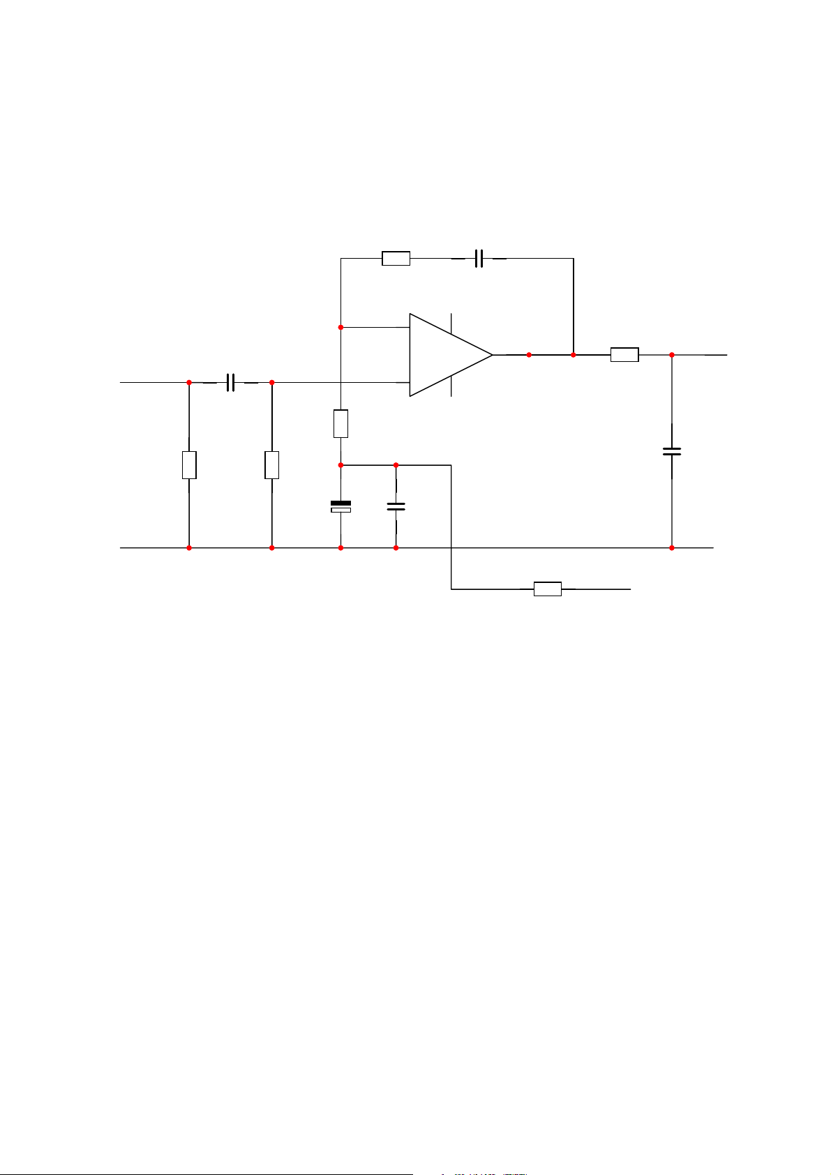
QUAD 405 Non-Inverting Input Modification
Sensitivity as shown is 1V
in for 100W output
R4 = 1.6k gives gives 0.5V
in for 100W output
keep C2 = 100u
C1
Input
680n
R1
220k
rms
rms
R3
22k
2%
Wire Link
R4
3.3k
2%
C2
47u
+
22k
R6
2%
2
3
-
+
C2B
3.3u
V+
V-
7
4
C4
680n
IC1
TL071
TLE2071
OPA604
OPA134
R12
6
R10
R5
4.7k
2%2.7.k
d.c from output
1n
C6
2%
The Following information is based on PCB type M12565 iss.3. The
layout can be applied to other versions but the instructions below
may not relate. See pictures at https://keith-snook.info
Cut track to op-amp close to pin 3, remove link pins and zenner
diodes D8 and D9.
Replace R10 with wire link, fit new values for R4, R6 and C4.
Fit new R3 standing upright such that it bridges R4 and fits between
end of C1 and the hole to ground where the link pin was removed.
Fit wire link from op-amp pin 3 to junction C1/R3, this can follow a
path against ground track.
Changing R12 to 2.7k inceases the frequency response to about
59kHz but this may not be suitable where the dumpers are "slowed
down" in versions where 1nF capacitor is placed across Tr10 BDY77.
 Loading...