


Π405
POWER AMPLIFIER Service Data
The Acoustical Manufacturing Co. Ltd. (Œ) Huntingdon, Cambridgeshire, PE29 6XU, England
Tel: +44(0)1480 447700 Fax: +44(0)1480 431767 www.quad-hifi.co.uk
Contents |
page |
|
Circuit Description |
3 |
|
Test Equipment |
4 |
|
Disconnecting Clamp Circuits |
4 |
|
Amplifier Circuit Testing |
5 |
|
Clamp Circuit Testing |
5 |
|
Fault Finding |
6 |
|
Modifications |
8 |
|
Clamp Circuit |
9 |
|
Replacing a Clamp Board |
9 |
|
Conversion of a 405 to a Mono 180 watt amplifier |
10 |
|
Replacing Transformer |
11 |
|
Replacing Amplifier Modules |
11 |
|
Π405-2 |
12 |
|
Assembly Diagram |
13 |
|
Circuit |
Diagram M12333 iss. 2 - Amplifier PCB M12368 iss. 5 & 6 |
14 |
Circuit |
Diagram M12333 iss. 3 - Amplifier PCB M12368 iss. 7 |
15 |
Circuit |
Diagram M12333 iss. 4 - Amplifier PCB M12368 iss. 9 |
16 |
Circuit |
Diagram M12333 iss. 5 - Amplifier PCB M12368 iss. 9 & 10 |
17 |
Amplifier Board layout M12368 iss. 9 & 10 |
18 |
|
Circuit |
Diagram M12333 iss. 6 - Amplifier PCB M12565 iss. 3 |
19 |
Amplifier Board layout M12565 iss. 3 |
20 |
|
Circuit |
Diagram M12333 iss. 7 - Amplifier PCB M12565 iss. 5 |
21 |
Circuit |
Diagram M12333 iss. 8 - Amplifier PCB M12565 iss. 6 |
22 |
Circuit |
Diagram M12333 iss. 9 - Amplifier PCB M12565 iss. 7 |
23 |
Circuit |
Diagram M12333 iss. 10 - Amplifier PCB M12565 iss. 7 |
24 |
Keith Snook modifications |
Click here |
|
2
CIRCUIT DESCRIPTION
The QUAD 405 is ã two channel power amplifier primarily intended for use in high quality sound reproducing systems. The amplifier is usually used with QUAD control units though other signal sources can readily be accommodated.
Û amplifier uses â current dumping output circuit, á Œ invention which eliminates many of Á problems associated with transistor amplifiers, and covered by patents in several countries.
In ä current dumping amplifier there is in effect both a low powered very high quality amplifier and a high powered heavy duty amplifier. Û low power amplifier controls the loudspeakers at all times, calling upon the high power section to provide most of the muscle. The small amplifier is so arranged - it carries an error signal - that provided the larger power transistors (the dumpers) get within the target area of the required output current it will fill in the remainder accurately and completely. The reproduced quality is solely dependent on thê small amplifier which because of its low power can be made very good indeed.
Problems of crossover, crossover distortion, quiescent current adjustment, thermal tracking, transistor matching, all disappear. Ûre are no internal adjustments or alignments and thë choice of power transistor types is less restrictive.
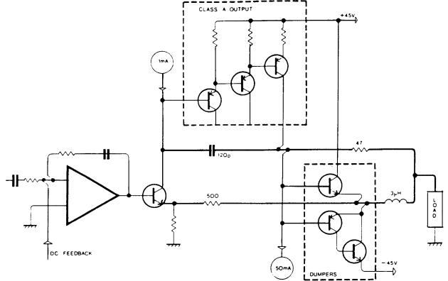
Fig. 1
Simplified Schematic of QUAD 405 Amplifier showing Class A, Dumpers and Bridge Components.
3
TEST EQUIPMENT
Sound Technology Distortion Analyser 1700A (ST1700A) Dual Beam Oscilloscope
4„ and 8„ load of 100W dissipation 1„ load of 25W dissipation
2.5 kHz Square Wave Generator
Input Sensitivity Indicator (0 to 1V RMS) AVOmeter (or similar multitester)
0 to 12V d.c. power supply Variac a.c. power supply
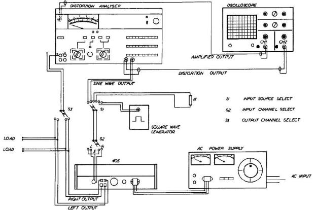
Fig. 2 illustrates a simple switching circuit which may assist if much testing is anticipated.
SUGGESTED SWITCHING ARRANGEMENT FOR TESTING QUAD405
Fig. 2
Before testing, Á cover of Á 405 should be removed.
DISCONNECTING CLAMP CIRCUITS
When servicing å 405 fitted with a clamp circuit, it may be necessary to bypass this circuit.
For 405s fitted with amplifier boards M12368, this may be done by removing t˙´ push-on connectors carrying Á brown wires from Á amplifier boards, and connecting Á loads between Á black output terminals and Á output terminals on Á amplifier boards.
For 405s fitted with amplifier boards type M12565, it will be necessary to remove thë side panels to gain access to Á printed copper side of Á amplifier boards. Á three screws securing each side panel should be removed, Á panel may thën bê slid outwards from Á amplifier. If Á solder is removed from Á link pad shown in Fig.18 (A), Á clamp circuit will become disconnected.
Care should be taken to ensure that when testing is completed, Á link pad is rë-soldered.
4
AMPLIFIER CIRCUIT TESTING M12368 - M12565
Á following test procedure is with reference to a 240V amplifier with no voltage limiters. Select:
Controls
ST 17OOA- |
Volts/power 100W RMS |
|
Distortion Ratio 0.01% |
|
8OkHz and 400Ï filters both in |
|
Frequency 1Ï |
|
Low Distortion |
|
Osc. level minimum |
Connections |
Load 8„ |
|
Sl Sine Wave (STl7OOA) |
|
S2 Left Input |
|
S3 Left Output |
If Á Amplifier fails any of t˙ë following tests, refer to Á appropriate pårt of Á fault finding section, page 6.
1.Check inside Á amplifier for obvious faults such as burnt components, blown internal fuses etc. Each of Á following checks should be repeated on t˙ê oÁr channel.
2.Apply Á a.c. Supply Volts whilst observing Á current consumptionformatwhich should not exceed 0.12A.
3.Increase thé oscillator level to 0.5V RMS ±0.5Î. Á output should be 100W with no sign of clipping.
4.Select set level ¶ adjust meter deflection for zero. Select distortion which should be less than 0.01% Select volts/power, decrease Á applied frequency to 100Hz, re ove 400Hz filter ¶ adjust osciIIoscope timebase to 2ms/cm. Set level, select distortion which should be less than 0.01%. Select volts/power, increase Á applied frequency to 3Ï, select 400Ó filter and adjust timebase to 50µs/cm. Select distortion which should again be less than 0.01%.
5.Select volts/power, increase applied frequency to 10kHz and adjust timebase2002to µs/cm. Adjust oscillator level so that output is 100W. Set level pdfÁnSnookselect distortion which should be less than 0.05%.
6.Select volts/power, increase applied frequency to 20kÓ and adjust Á timebase to 10µs/cm. Reduce output level to 80W. Set level and measure distortion which sh uld be less than .1%.
Select volts/power and decrease frequency to 1kHz. Adjust scillat r level so that output is 100W and
adjust timebase to 0.2ms/cm. Û followinginchecks are to m nit r Á low frequency roll off of Á 405. Select 30Ó and Á output level should fall by approximately 0.3dB. Select 0Hz and Á output level
should fall by approximately 1Î. Select 10Ó and Á output level should. fall by 7dB ± 1.5dB.7.
8.Increase frequency to 1Ï. For 405s with amplifier boards type M12368 insert 1.8k„ voltage limiting
resistors into Á mini sockets on each amplifier board. For 405s with amplifier boards type M12565-3 insert a link into Áse sockets. Û output waveform should indica e clipping. Reduce Á oscillator levelltd
|
|
Keith |
13. CLAMPReproducedCIRCUIT TESTING |
||
|
~daylight |
|
|
until Á clipping just disappears at which po nt Á output level should be 20V RMS ±1V. Remove voltage |
|
|
voltage limitters, and adjust os illator lev for 100W output. |
|
9. |
Select volts/power ¶ sq are wave input, (S1). Adjust timebase to 0.1ms/cm. Remove load and note |
|
|
Á difference in Á waveform with load and no load. Áre should be a slight difference in gain (10mV) but |
|
|
no overshoot. Rec nnect the 8„ load. |
|
10. |
by |
|
Û following checks sh uld be carried out with no input signal and Á input to thë amplifier board loaded by |
||
a 1k„ resistor, (S1). Remove 400Hz filter and select noise which should bê better than -93Î unweighted.
11. Select volts/ ower, 400Hz filter and sine wave input at å frequency of 1Ï and adjust oscillator level for 100W output. Select 1„ load. Á output should clip equally on both halves of th´ waveform as
shown in Fig. 11. |
|
. |
|
|
|
||
12. Select 4„ load, output level should be 70W just prior to clipping. |
|||
|
.circuit, |
|
|
|
d |
|
Á circuit should first be disconnected from its amplifier board, äs |
ln order to test Á clamp |
|
||
described on page 4. |
|
|
|
For 405s fitted with amplifier boards M12368 apply 6V d.c. across Á output terminals of Á relevant channel with an ammeter in circuit.
For 405s fitted with amplifier boards M12565 ä wire should be soldered across Á back of Á amplifer board as shown in Fig. 18(B). 6V d.c. should be applied between this wire and Á black output terminal of Á relevant channel, with an ammeter in circuit.
In both cases Á current should not exceed 0.5mA. Reverse thë polarity of Á supply and repeat Á test. Û test should Án be carried out on Á oÁr channel.
T˙ê complete test should thén be repeated using a 12V d.c. supply with a 10„ resistor in series, when Á current should be approximately 1A.
5
FAULT FINDING
The following information may assist in locating faults occuring on the amplifier boards of a 405.
In each case only the faulty channel of the 405 is driven, as in the test procedure. The input should be
a sine wave of 0.5V |
MS an |
th |
t |
t sh l |
b a |
|
lied to an 8„ load unless otherwise stated. |
|||||||||
The numbers refer t |
th |
|
lav |
nt t st |
h |
k. |
|
|
|
|
|
|
|
|||
*Board type M12368 |
nly **B a ty |
M12565 |
nly. |
|
|
|
|
|
|
|||||||
Effect |
|
|
|
|
|
|
|
|
|
Ca |
|
se |
|
|
|
|
1. |
|
|
|
|
|
|
|
|
|
|
|
|
|
|
|
|
R33 Burnt |
|
|
|
|
|
|
|
|
|
C ll ctor-Base Tr10 o/c |
||||||
R37 Burnt |
d |
|
|
|
|
|
|
|
L1 |
|
/c (solder joints) |
|
||||
R41 Burnt |
|
|
|
|
|
|
|
L3 |
|
/c (solder joints) |
|
|||||
R39 Burnt |
|
|
|
|
|
|
|
20 or R21 o/c |
|
|||||||
R38 Burnt |
|
|
|
|
|
|
|
D5 |
|
r D6 o/c |
|
|||||
|
. |
|
|
by |
|
|
|
|
||||||||
|
|
|
|
|
|
|
|
|
|
|
|
|
||||
2. |
|
c |
|
|
|
|
|
|
|
|
|
|
||||
|
|
. |
|
|
|
|
|
|
|
|
|
|||||
High Current |
|
|
|
|
|
T 2 o/c, Tr3 o/c, Tr7 o/c Tr9 s/c |
||||||||||
|
|
|
|
|
|
|
|
|||||||||
|
|
|
|
|
|
|
|
|
|
T 10 s/c, R7 o/c C8 s/c |
||||||
* |
|
|
ReproducedC3 s/c |
|
|
|
||||||||||
** |
|
|
|
|
|
|
|
|
|
D2 o/c R8 o/c |
|
|||||
Draws high current w |
c |
|
rops |
o 0.1A |
|
|
|
in |
|
|
||||||
after approx 2 secon s |
|
|
|
|
|
|
|
|
||||||||
|
|
|
|
|
R14 o/c |
|
|
|
||||||||
3. |
|
|
|
|
|
|
Keith |
|
|
|
|
|
|
|||
|
|
|
|
|
|
|
|
|
|
|
|
|
|
|
|
|
No increase in a.c. supp |
curren |
|
|
|
|
|
|
|
|
|
|
|||||
for increase in signal |
|
|
|
|
|
|
R3 |
|
/c, C1 |
/c, R31 |
/c |
|||||
Signal is unstable an |
c ps |
|
|
|
|
R6 |
|
/c |
||||||||
100W output for 0.3V~daylightnpu |
R20 |
|
r R21 |
/c |
|
|||||||||||
Waveform trace as in Fig. 3 |
|
|
|
Tr8 |
/c, Tr6 s/c, R36 |
/c, R30 /c, C10 s/c |
||||||||||
Waveform trace as in Fig. 4 |
|
|
|
L2 |
|
/c (s lder j i ts) |
|
|||||||||
Approximately 4W output |
|
|
|
|
|
R16 |
|
/c |
|
|
|
|||||
|
|
|
|
|
|
|
|
|
ltd |
|
|
|
|
|||
4. |
|
|
|
|
|
|
|
|
|
Snook. |
||||||
Second Harmonic Distortion |
|
|
|
|
IC1, Tr1, Tr |
, Tr3, Tr4, R5, R6, R17, R18, R22, C1 |
||||||||||
Second Harmonic Distortion especially at 100Ó |
C2, C7, C8 |
format |
|
and on o/c load |
|
|
|
Third Harmonic Distortion especially at 100Ó |
R5 |
|
|
|
|
||
Third Harmonic Distortion |
L2, R3, R6, R16, R , R 1, C3 |
||
Hum and Noise |
C5 o/c |
|
|
Hum* |
R37 o/c |
|
|
Waveform trace as in Fig. 5* |
|
2002 |
|
Tr3 s/c |
|
||
Waveform trace as in Fig. 6* |
R23 o/c, R5 o/c |
|
|
Waveform trace as in Fig. 7 |
R33 s/c |
|
|
Waveform trace as in Fig. 8* |
R8 o/c |
|
|
Waveform trace as in Fig. 9 |
C5 s/c, R15 o/c, Tr1 o/c |
||
6. |
|
|
|
Distortion at 20Ï |
D5 or D6 s/c, |
|
|
8. |
|
|
|
Liimiting resistor R11 has no effect |
R10 s/c |
|
|
9. |
|
|
|
Square Wave trace as in Fig. 10 |
C6 o/c |
|
|
10. |
|
|
|
Noise especially at 100Ó |
R5 |
|
|
Noise with large spikes |
Tr1 |
|
|
Noise |
R12, R3, R4, Tr2, IC1 (change to topology!) |
||
11. |
|
|
|
Current limiting check with 1„ load |
|
|
|
Waveform trace as in Fig. 12 |
R29 o/c, R28 s/c, R25 o/c |
||
Waveform trace as in Fig. 13 |
D3 s/c, R27 o/c, R24 o/c, R26 s/c |
||
Waveform trace as in Fig. 14 |
Tr6 o/c |
|
|
Waveform trace as in Fig. 8 |
C11 s/c Tr5 o/c |
|
|
13. |
|
|
|
Draws high current with 6V d.c. supply |
T2 s/c |
|
|
™
6

7
MODIFICATIONS TO PRINTED CIRCUIT BOARDS.
Amplifier Board M12368 iss.5 originally fitted. |
Circuit diagram iss. 2. |
1.Amplifier board M12368 iss.6
Copper track layout modified - component layout ünchanged.
2. |
Amplifier board M12368 iss.7 |
Circuit diagram iss. 3. |
|
R4 changed from 10k to 22k |
|
|
R5 changed from 10k to 4k7 |
|
|
R9 changed from 180„ to 220„ |
|
|
R19 (3k3) removed (combined with R23) |
|
|
R23 changed from 3k3 to 1k2 |
|
|
C9 (330pF) removed (would be in parallel with C11) |
|
|
C18 47nF fitted to -ve supply after FS2 - see circuit diagram |
|
|
FS1 and FS2 effectively changed places |
|
|
R2 changed from 2.2„ to 10„ |
|
|
Copper track width reduced |
|
3.(a) |
Amplifier board M12368 iss.9 introduced ¤ serial number 9000. |
Circuit diagram iss. 4. |
|
R41 22„ added |
|
|
L3 6.9µH added |
|
|
C15 0.1µF added |
|
|
C16 0.1µF added |
|
|
C18 (47nF) removed |
|
|
C19 1nF fitted between base and collector of Tr10 (not recommended if stable without) |
|
|
Copper track width reduced |
|
|
Also at s/n 9000 a clamp circuit, on PCB M12400, was mounted on the output terminal (Fig. 15). |
|
|
This detects excessive d.c. offset at the output and short circuits, blowing the internal 4A fuses |
|
|
FS1 and/or FS2 to protect the loudspeaker. |
|
3.(b) |
The following component changes were made ¤ serial number 29000. |
Circuit diagram iss. 5. |
|
R10 changed from 1k to 1k8 |
|
|
R27 changed from 8k2 to 15k |
|
|
R29 changed from 8k2 to 15k |
|
|
R35 changed from 0.08„ to 0.091„ |
|
|
R36 changed from 0.08„ to 0.091„ |
|
D1 changed from LR120C to LR150C (op-amp voltage increased from 12V to 15V) D2 changed from LR120C to LR150C (op-amp voltage increased from 12V to 15V)
4.Amplifier board M12368 iss.10
Identical to M12368 iss. 9 except copper pads for power transistors modified for production.
5. |
Amplifier board M12565 |
iss.3 Introduced at serial number 59001. |
Circuit diagram iss. 6. |
|
Other QUAD 405s with this PCB fitted were serial numbers 57301 to 57600 inc. |
||
|
This board incorporates the clamp circuit and the ESL voltage limiter is now a link |
||
6. |
Amplifier board M12565 |
iss.5 (Π405-2 PCB). |
Circuit diagram iss. 7. |
Was fitted at serial number 62500 but with a 405 name plate until serial number 65000. See page 12 for 405-2 PCB changes.
Alternatives
Transistors - on PCB M12368 iss. 5, 6 & 7 BDY77 or BDY74 may have been used for Tr9 and Tr10. BDY77 is a suitable replacement for both but beware - faster transistors may cause instabiliity.
On M12368 iss. 9 &10 and M12565 iss. 3 Transistors Tr9 and Tr10 may be 2SD424, 17556 or 2SD676 and are interchangeable.
Tr2 - BC682, ZTX304, BCX32 and BC546B are interchangeable. Tr3, Tr4 - E5458, ZTX504 and BC556B are interchangeable.
Tr7, Tr8 - 40872 or 2SA740 are interchangeable.
LED - LP1 - HP5082-4850, Exciton XC5053, Toshiba TLR114A (or any modern LED with R40 adjusted).
8
 Loading...