

PTC PT2399, PT2399S, PT2399-SN Schematics
PT2399
Echo Processor IC
DESCRIPTION
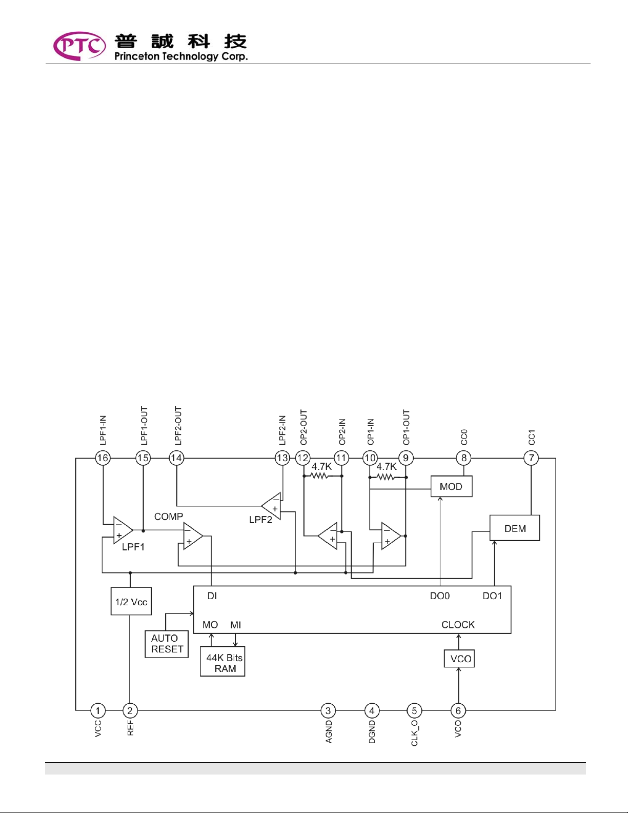
The PT2399 is a single chip echo processor IC utilizing
CMOS technology. Which accept analog audio input
signal, a high sample rate ADC transfer the analog
signal into a bit stream then storage to internal 44Kbit
RAM, after processing the bit stream will de-modulate
by DAC and lowpass filter. Overall delay time is
determined by internal VCO clock frequency, and user
can easy to change the VCO frequency by changing
the external resistance. The PT2399 performs low
distortion (THD<0.5%@0.5Vrms) and low noise
(No<-90dBV) characteristic for audio purpose, and pin
arrangement and application circuit are optimized for
easy PCB layout and cost saving advantage.
APPLICATIONS
• KARAOKE Mixer
• CD/DVD Player/Recorder
• Multimedia TV
• Car Entertainment System
• Music Instrument effecter
• Electronics Toy
FEATURES
• CMOS technology
• Least external components
• Auto reset Function prevent POP noise
• Low noise, SNR better than 90dB (typical)
• Low distortion, THD= 0.5%(typical)
• User adjustable VCO clock frequency.
BLOCK DIAGRAM
Tel: 886-66296288‧Fax: 886-29174598‧ http://www.princeton.com.tw‧2F, 233-1, Baociao Road, Sindian, Taipei 23145, Taiwan
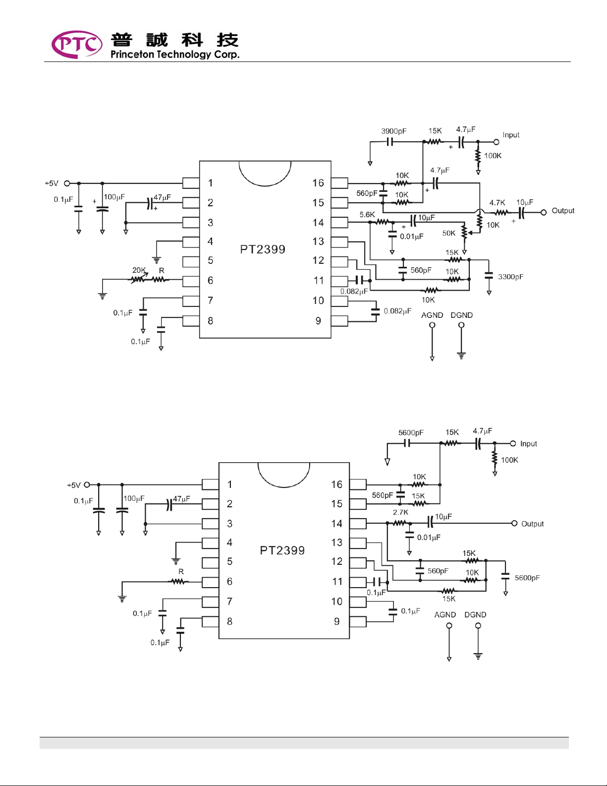
APPLICATION CIRCUIT
ECHO
PT2399
Note:
External Resistor having a value of 10 K to 50 K may be used. The recommended Resistor Value(R) is 10 K. When the value of the Resistor (R)
increases, the range of the Delay Time also increases.
SURROUND/DELAY
Note: Please refer to Table 1 for the Resistor/Delay Time values.
V1.6 2 February 2010
ORDER INFORMATION
Valid Part Number Package Type Top Code
PT2399 16 Pins, DIP, 300mil PT2399
PT2399S 16 Pins, SOP, 300mil PT2399S
PT2399-SN 16 Pins, SOP, 150mil PT2399-SN
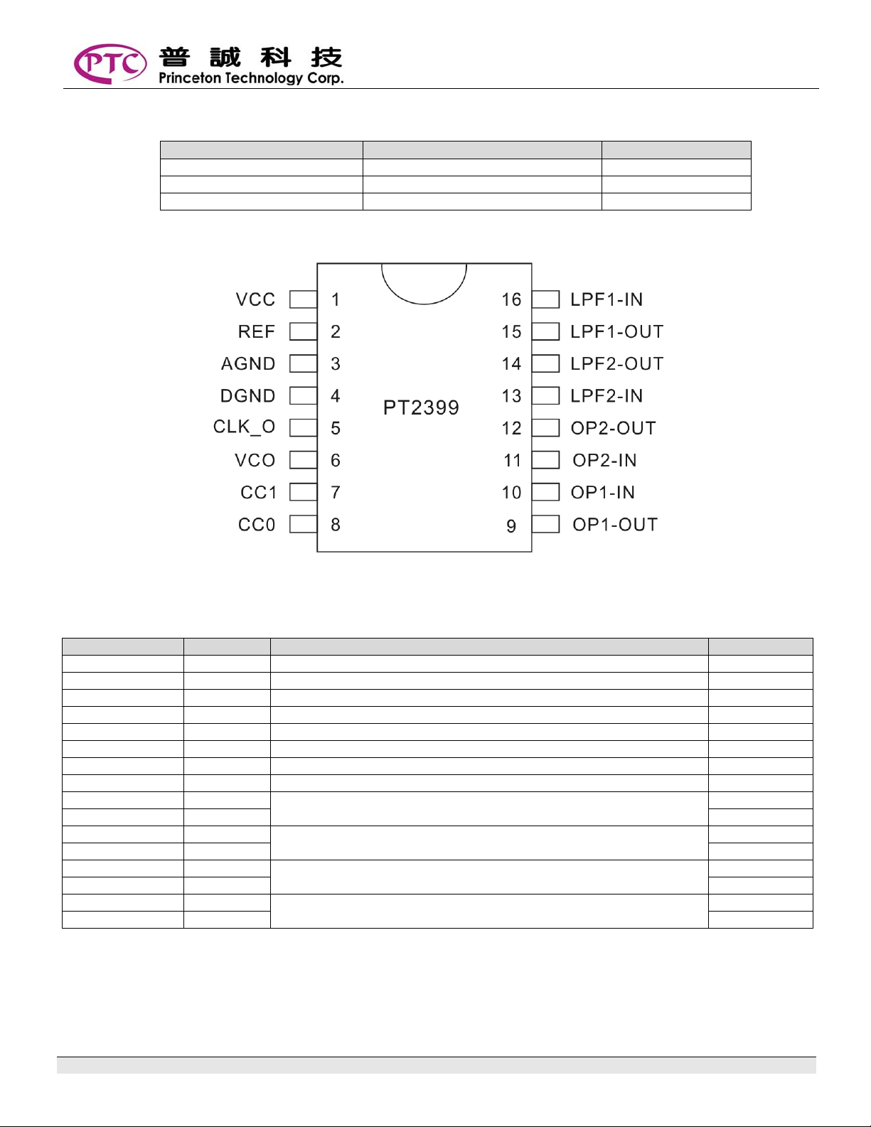
PIN CONFIGURATION
PT2399
PIN DESCRIPTION
Pin Name I/O Description Pin No.
VCC - Analog supply voltage input 1
REF - Analog reference voltage (1/2VCC) 2
AGND - Analog ground 3
DGND - Digital ground 4
CLK_O O System clock output pin 5
VCO I VCO Frequency adjustment 6
CC1 - Current control 1 7
CC0 - Current control 0 8
OP1-OUT O OP amplifier 1 input/output. This pin can be used as
OP1-IN I 10
OP2-IN I OP Amplifier 2 input/output. This pin can be used as
OP2-OUT O 12
LPF2-IN I
LPF2-OUT O 14
LPF1-OUT O
LPF1-IN I 16
modulated/Demodulated integrator by connecting capacitor
Modulated/Demodulated Integrator by connecting Capacitor
Low pass filter 2 input/output pin
Low pass filter 1 input/output pin
9
11
13
15
V1.6 3 February 2010
 Loading...