

PTC PT2313, PT2313-S Schematics

PTC Princeton Technology Corp. Tel : 886-2-29162151
Fax : 886-2-29174598
4-Channel Audio Processor IC PT2313
Description
PT2313 is an four-channel digital audio processor utilizing CMOS Technology. Volume,
Right/Left Bass and Treble Balance, Front/Rear Fader Processor are incorporated into a single
chip. Loudness Function and Selectable Input Gain are also provided to build a highly effective
electronic audio processor having the highest performance and reliability with the least external
components. All functions are programmable using the Serial Bus. The pin assignments and
application circuit are optimized for easy PCB layout and cost saving advantage for audio
application. PT2313 is housed in a 28-pin DIP/SO Package and is functionally compatible with
TDA7313.
Features
r CMOS Technology
r Least External Components
r Treble and Bass Control
r Loudness Function
r 3 Stereo Inputs with Selectable Input Gain
r Input/Output for External Noise Reduction System/Equalizer
r 4 Independent Speaker Controls for Fader and Balance
r Independent Mute Function
r Volume Control in 1.25 dB/step
r Low Distortion
r Low Noise and DC Stepping
r Controlled by Serial Bus Micro-Processor Interface
Applications
r Car Stereo (Audio)
r Hi-Fi Audio System
PT2313 v 1 Page 1 Written Feb. 1997
PTC Princeton Technology Corp. Tel : 886-2-29162151
Fax : 886-2-29174598
4-Channel Audio Processor IC PT2313
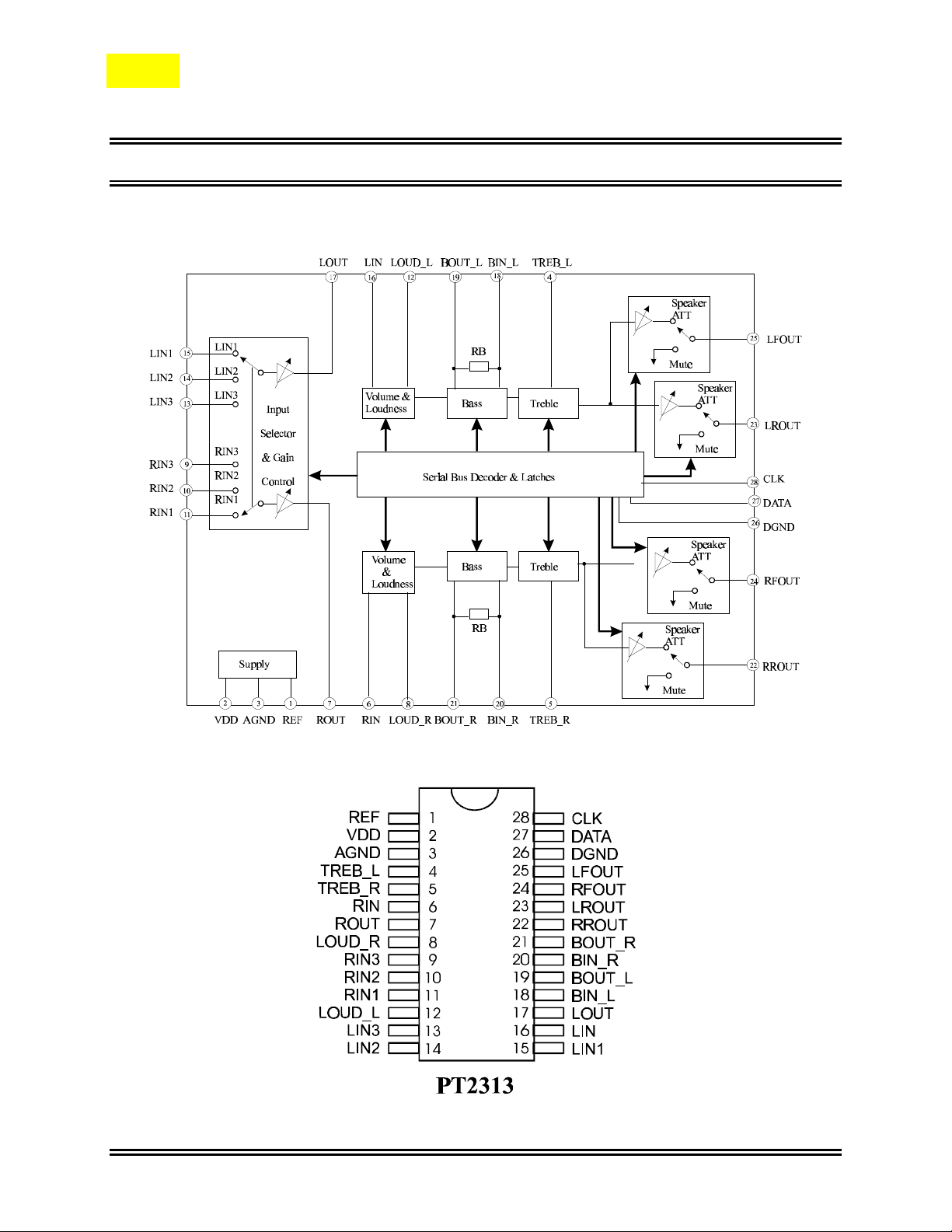
Block Diagram
Pin Configuration
PT2313 v 1 Page 2 Written Feb. 1997
PTC Princeton Technology Corp. Tel : 886-2-29162151
Fax : 886-2-29174598
4-Channel Audio Processor IC PT2313
Pin Description
Pin Name I/O Description Pin No.
REF - Analog Reference Voltage (1/2 VDD) 1
VDD - Supply Input Voltage 2
AGND - Analog Ground 3
TREB_L I Left Channel Input for Treble Controller 4
TREB_R I Right Channel Input for Treble Controller 5
RIN I Audio Processor Right Channel Input 6
ROUT O
LOUD_R I Right Channel Loudness Input 8
Gain Output and Input Selector for Right
Channel
7
RIN3 I Right Channel Input 3 9
RIN2 I Right Channel Input 2 10
RIN1 I Right Channel Input 1 11
LOUD_L I Left Channel Loudness Input 12
LIN3 I Left Channel Input 3 13
LIN2 I Left Channel Input 2 14
LIN1 I Left Channel Input 1 15
LIN I Audio Processor Left Channel Input 16
LOUT O
BIN_L I Left Bass Controller Input Channel 18
BOUT_L O Left Bass Controller Output Channel 19
BIN_R I Right Channel Input for Bass Controller 20
BOUT_R O Right Channel Output for Bass Controller 21
RROUT O Right Rear Speaker Output 22
LROUT O Left Rear Speaker Output 23
Gain Output and Input Selector for Left
Channel
17
RFOUT O Right Front Speaker Output 24
LFOUT O Left Front Speaker Output 25
DGND - Digital Ground 26
DATA I Control Data Input 27
CLK I Clock Input for Serial Data Transmission 28
PT2313 v 1 Page 3 Written Feb. 1997
PTC Princeton Technology Corp. Tel : 886-2-29162151
Fax : 886-2-29174598
4-Channel Audio Processor IC PT2313
Functional Description
Bus Interface
Data are transmitted to and from the microprocessor to the PT2313 via the DATA and
CLK. The DATA and CLK make up the BUS Interface. It should be noted that the pullup resistors must be connected to the positive supply voltage.
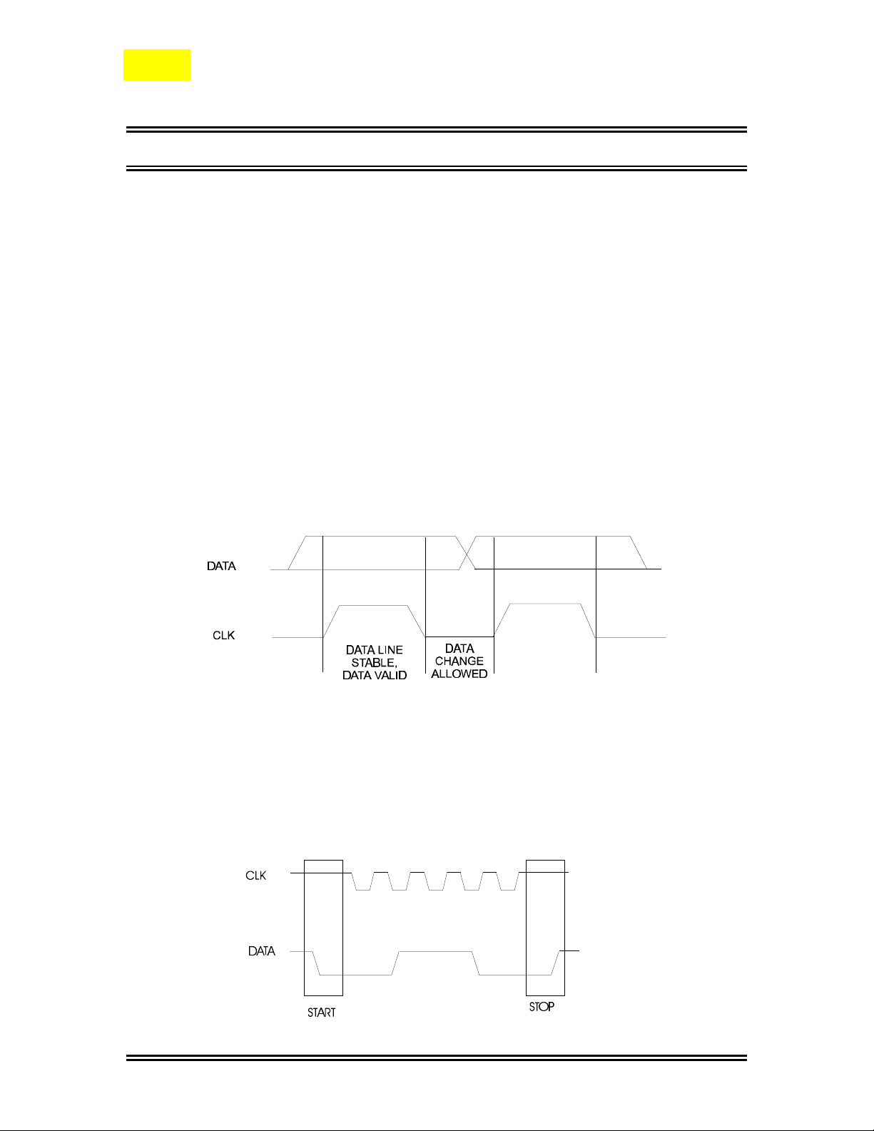
Data Validity
A data on the DATA Line is considered valid and stable only when the CLK Signal is in
HIGH State. The HIGH and LOW State of the DATA Line can only change when the
CLK signal is LOW. Please refer to the figure below.
Start and Stop Conditions
A Start Condition is activated when 1) the CLK is set to HIGH and 2) DATA shifts
from HIGH to LOW State. The Stop Condition is activated when 1) CLK is set to
HIGH and 2) DATA shifts from LOW to HIGH State. Please refer to the timing diagram
below.
PT2313 v 1 Page 4 Written Feb. 1997
PTC Princeton Technology Corp. Tel : 886-2-29162151
Fax : 886-2-29174598
4-Channel Audio Processor IC PT2313
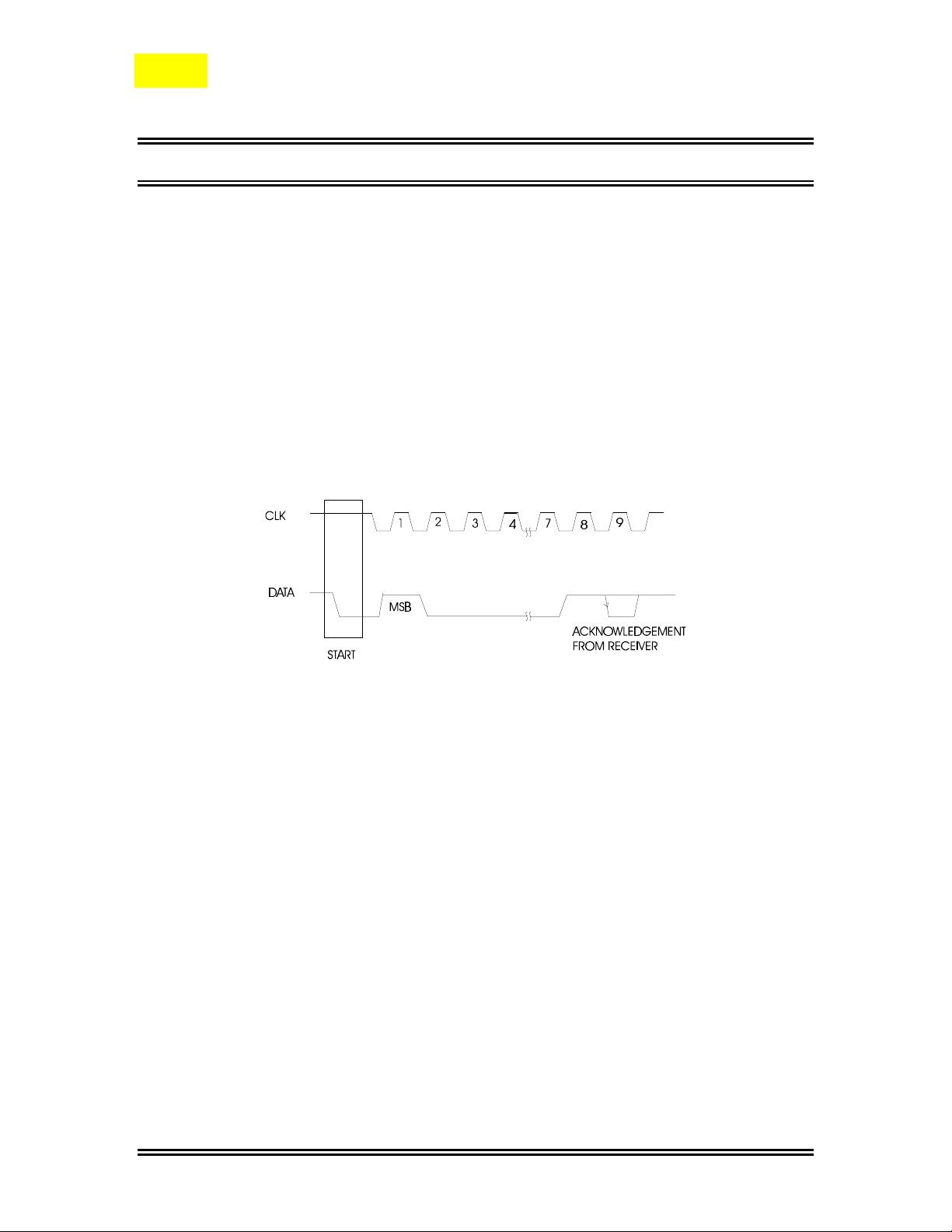
Byte Format
Every byte transmitted to the DATA Line consist of 8 bits. Each byte must be followed
by an Acknowledge Bit. The MSB is transmitted first.
Acknowledge
During the Acknowledge Clock Pulse, the master (µP) puts a resistive HIGH level on the
DATA Line. The peripheral (audio processor) that acknowledges has to pull-down
(LOW) the DATA line during the Acknowledge Clock Pulse so that the DATA Line is in
a Stable Low State during this Clock Pulse. Please refer to the diagram below.
The audio processor that has been addressed has to generate an acknowledge after
receiving each byte, otherwise, the DATA Line will remain at the High Level during the
ninth (9th) Clock Pulse. In this case, the master transmitter can generate the STOP
Information in order to abort the transfer.
Transmission without Acknowledge
If you want to avoid the acknowledge detection of the audio processor, a simpler µP
transmission may be used. Wait one clock and do not check the slave acknowledge of
this same clock then send the new data. If you use this approach, there are greater
chances of faulty operation as well as decrease in noise immunity.
Interface Protocol
The interface protocol consists of the following:
• A Start Condition
• A Chip Address Byte including the PT2313 address. The 8th Bit of the Byte must be
“0”. PT2313 must always acknowledge the end of each transmitted byte.
PT2313 v 1 Page 5 Written Feb. 1997
 Loading...