

PTC AV100 Service Manual LM4731
LM4731
Stereo 25W Audio Power Amplifier with Mute and
Standby Modes
LM4731 Stereo 25W Audio Power Amplifier with Mute and Standby Modes
November 2002
General Description
The LM4731 is a stereo audio amplifier capable of delivering
typically 25W per channel of continuous average output
power into a 4Ω or 8Ω load with less than 10% THD+N from
20Hz - 20kHz.
Each amplifier has an independent smooth transition fade-in/
out mute and a power conserving standby mode which can
be controlled by external logic.
The LM4731 has short circuit protection and a thermal shut
down feature that is activated when the die temperature
exceeds 150˚C. The LM4731 also has a under voltage lock
out feature for click and pop free power off and on.
The LM4731 has a wide operating supply range from +/-10V
- +/-28V allowing for lower cost unregulated power supplies
to be used.
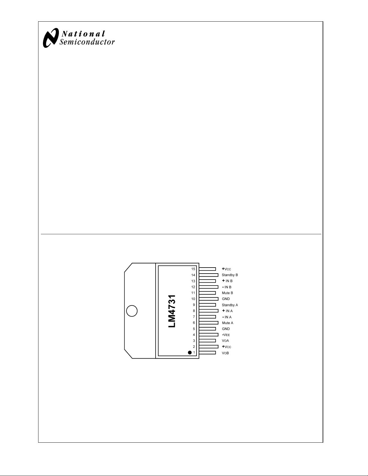
Connection Diagram
Plastic Package
Key Specifications
n Output power into 4Ω or 8Ω, 10% THD+N 25W (typ)
n THD+N at 1kHz with2x1Winto 8Ω 0.02% (typ)
n Mute Attenuation 85dB (typ)
n PSRR with f
n Slew Rate 18V/µs (typ)
n Standby Current (+/-22V) 4.8mA (typ)
RIPPLE
= 120Hz, V
RIPPLE
=1V
50dB (typ)
RMS
Features
n Minimal amount of external components necessary
n Quiet fade-in/out mute mode
n Low current Standby-mode
Applications
n Audio amplifier for high-end stereo TVs
n Audio amplifier for component stereo
n Audio amplifier for compact stereo
n Audio amplifier for PC satellite speaker systems
n Audio amplifier for self powered speakers
Top View
Non-Isolated Package
Order Number LM4731TA
See NS Package Number TA15A
© 2002 National Semiconductor Corporation DS200603 www.national.com
20060352
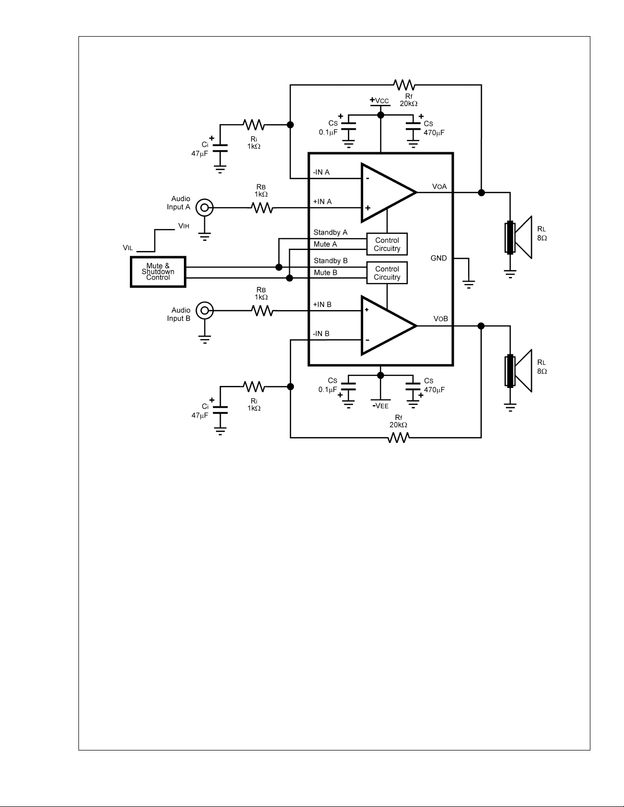
Typical Application
LM4731
FIGURE 1. Typical Audio Amplifier Application Circuit
20060353
www.national.com 2
LM4731
Absolute Maximum Ratings (Notes 1,
2)
If Military/Aerospace specified devices are required,
please contact the National Semiconductor Sales Office/
Distributors for availability and specifications.
+
Supply Voltage |V
Common Mode Input Voltage V
Differential Input Voltage 56V
Output Current Internally Limited
Power Dissipation (Note 3) 50W
ESD Susceptability (Note 4) 2.0kV
|+|V-| 56V
+
or V
-
T Package (10 sec.) 260˚C
Storage Temperature −40˚C to +150˚C
Thermal Resistance
θ
(TA) 43˚C/W
JA
θ
(TA) 1.5˚C/W
JC
Operating Ratings (Notes 1, 2)
Temperature Range
T
≤ TA≤ T
MIN
Supply Voltage |V
MAX
+
|+|V-| 20V ≤ V
−20˚C ≤ TA≤ +85˚C
TOTAL
ESD Susceptability (Note 6) 250V
Junction Temperature (T
) (Note 9) 150˚C
JMAX
Soldering Information
Electrical Characteristics (Notes 1, 2)
The following specifications apply for V+= +22V, V-= −22V and RL=8Ω unless otherwise specified. Limits apply for TA=
25˚C.
Symbol Parameter Conditions LM4731 Units
Typical Limit
(Note 6) (Notes 7, 8)
+
|+|V-| Power Supply Voltage (Note 10) GND − V-≥ 9V 20
|V
56
(Limits)
V (min)
V (max)
≤ 56V
A
M
P
O
THD+N
X
talk
Mute Attenuation 85 dB
Output Power (RMS)
Total Harmonic Distortion +
Noise
Channel Separation
SR Slew Rate (Note 11) V
I
DD
Total Quiescent Power Supply
Current
V
OS
I
B
Input Offset Voltage VCM= 0V, IO= 0 mA 2.0 15 mV (max)
Input Bias Current VCM= 0V, IO= 0 mA 0.2 µA
PSRR Power Supply Rejection Ratio V
A
VOL
e
IN
Open Loop Voltage Gain RL=2kΩ, ∆ VO= 20V 110 dB
Input Noise IHF — A-Weighting Filter 2.0 8 µV (max)
Standby
V
IL
V
IH
Standby Low Input Voltage Not in Standby Mode (Play) 0.8 V (max)
Standby High Input Voltage In Standby Mode 2.0 2.5 V (min)
THD+N = 10% (max), f = 1kHz
+
|V
|=|V-| = 18V, RL=4Ω
+
|=|V-| = 22V, RL=8Ω
|V
THD+N = 1% (max), f = 1kHz
+
|=|V-| =18V, RL=4Ω
|V
+
|=|V-| = 22V, RL=8Ω
|V
= 1W, f = 1kHz
P
O
= 26dB,
A
V
+
|=|V-| = 18V, RL=4Ω
|V
+
|=|V-| = 22V, RL=8Ω
|V
P
= 10W
O
f = 1kHz
f = 10kHz
IN
= 2.0V
p-p,trise
= 2ns 18 V/µs
VCM= 0V, VO= 0V, IO=0A
Standby off (Play Mode)
Standby on (Standby Mode)
RIPPLE
=1V
RMS,fRIPPLE
= 120Hz sine
wave
Inputs terminated to GND
R
= 600Ω (Input Referred)
IN
25
25
20
20
0.03
0.02
20
22
18
18
0.5
0.3
W (min)
W (min)
W (min)
W (min)
% (max)
% (max)
65
60
95
4.8
110
6
mA (max)
mA (max)
50 dB
dB
dB
www.national.com3
Electrical Characteristics (Notes 1, 2) (Continued)
The following specifications apply for V+= +22V, V-= −22V and RL=8Ω unless otherwise specified. Limits apply for TA=
LM4731
25˚C.
Symbol Parameter Conditions LM4731 Units
Typical Limit
(Note 6) (Notes 7, 8)
Mute
V
IL
V
IH
Note 1: All voltages are measured with respect to the ground pin, unless otherwise specified.
Note 2: Absolute Maximum Ratings indicate limits beyond which damage to the device may occur. Operating Ratings indicate conditions for which the device is
functional, but do not guarantee specific performance limits. Electrical Characteristics state DC and AC electrical specifications under particular test conditions which
guarantee specific performance limits. This assumes that the device is within the Operating Ratings. Specifications are not guaranteed for parameters where no limit
is given. However, the typical value is a good indication of a device’s performance.
Note 3: The maximum power dissipation must be de-rated at elevated temperatures and is dictated by T
allowable power dissipation is P
and the typical θ
Note 4: Human body model, 100 pF discharged through a 1.5 kΩ resistor.
Note 5: Machine Model: a 220pF - 240pF discharged through all pins.
Note 6: Typical specifications are sepcified at 25˚C and represent the parametric norm.
Note 7: Tested limits are guaranteed to National’s AOQL (Average Outgoing Quality Level).
Note 8: Datasheet min/max specification limits are guaranteed by design, test, or statistical analysis.
Note 9: The operating junction temperature maximum is 150˚C. However, the instantaneous Safe Operating Area temperature is 250˚C.
Note 10: V
differential between V
Note 11: The feedback compensation network limits the bandwidth of the closed-loop response causing the skew rate to be reduced by the high frequency roll-off.
Without feedback compensation the slew rate is typically larger.
Note 12: The LM4731TA package TA15A is a non-isolated package setting the tab of the device and the heat sink to V-potential when the LM4731TA is directly
mounted to the heat sink using only thermal compound. If a mica washer is used in addition to thermal compound, θ
will be electrically isolated from V-.
Mute Low Input Voltage Not in Mute Mode (Play) 0.8 V (max)
Mute High Input Voltage In Mute Mode 2.0 2.5 V (min)
, θJC, and the ambient temperature TA. The maximum
=(T
is 1.5˚C/W for the TA15A package . Refer to the Thermal Considerations section for more information.
JC
-
must have at least -9V at its pin with reference to GND in order for the under-voltage protection circuitry to be disabled. In addition, the voltage
DMAX
+
and V-must be greater than 14V.
)/θJCor the number given in the Absolute Maximum Ratings, whichever is lower. For the LM4731, T
JMAX-TA
JMAX
(case to sink) is increased, but the heat sink
CS
(Limits)
= 150˚C
JMAX
Bridged Amplifier Application Circuit
20060305
FIGURE 2. Bridged Amplifier Application Circuit
www.national.com 4
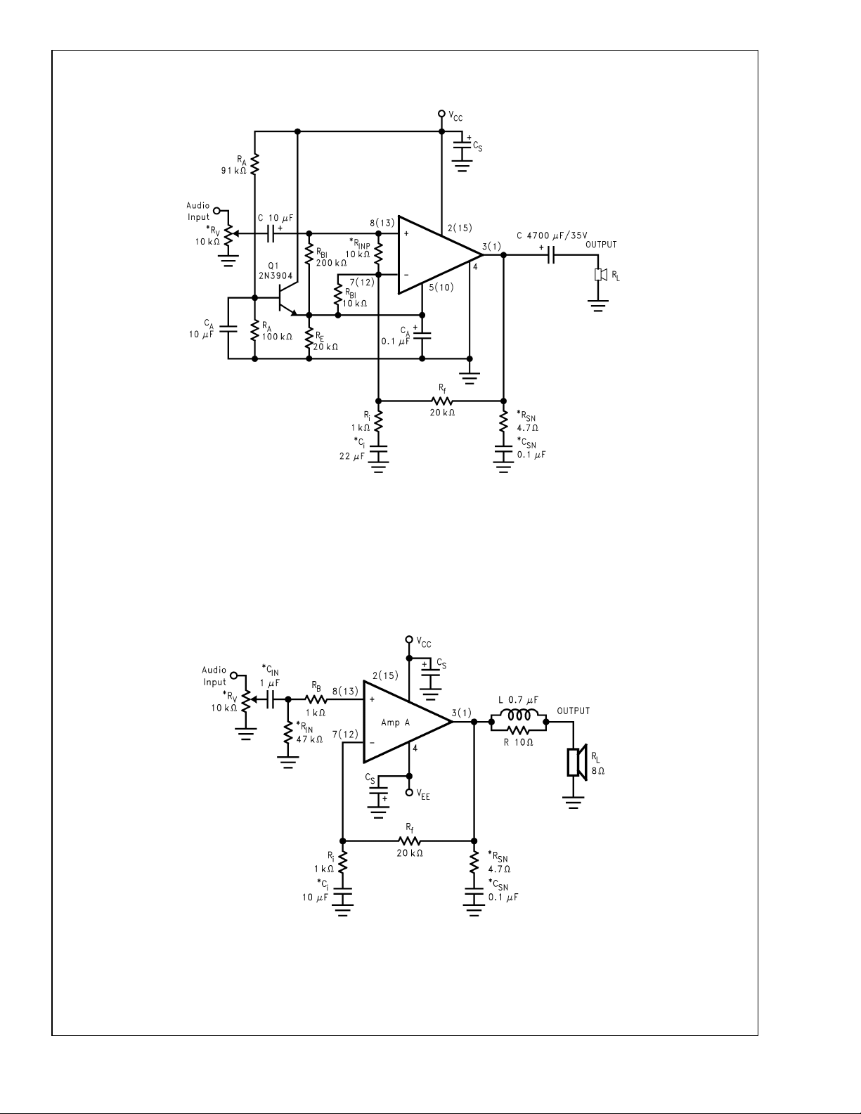
Single Supply Application Circuit
LM4731
FIGURE 3. Single Supply Amplifier Application Circuit
Note:*Optional components dependent upon specific design requirements.
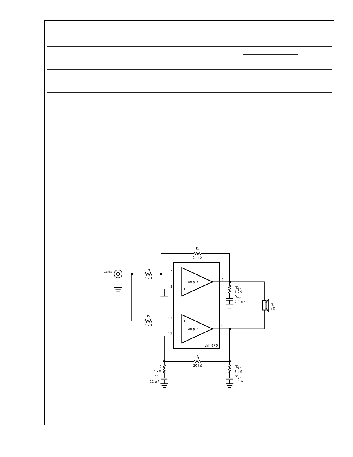
Auxiliary Amplifier Application Circuit
20060306
FIGURE 4. Special Audio Amplifier Application Circuit
20060307
www.national.com5
 Loading...