


Power Integrations TOP243P, TOP243G, TOP243G-TL, TOP242Y, TOP242R-TL Datasheet
...TOP242-249 |
® |
|
TOPSwitch®-GX Family
Extended Power, Design Flexible,
EcoSmart®, Integrated Off-line Switcher
Product Highlights
Lower System Cost, High Design Flexibility
•Extended power range to 250 W
•Features eliminate or reduce cost of external components
•Fully integrated soft-start for minimum stress/overshoot
•Externally programmable accurate current limit
•Wider duty cycle for more power, smaller input capacitor
•Separate line sense and current limit pins on Y/R packages
•Line under-voltage (UV) detection: no turn off glitches
•Line overvoltage (OV) shutdown extends line surge limit
•Line feed forward with maximum duty cycle (DCMAX) reduction rejects line ripple and limits DCMAX at high line
•Frequency jittering reduces EMI and EMI filtering costs
•Regulates to zero load without dummy loading
•132 kHz frequency reduces transformer/power supply size
•Half frequency option in Y/R packages for video applications
•Hysteretic thermal shutdown for automatic fault recovery
•Large thermal hysteresis prevents PC board overheating
EcoSmart - Energy Efficient
•Extremely low consumption in remote off mode (80 mW @ 110 VAC, 160 mW @ 230 VAC)
•Frequency lowered with load for high standby efficiency
•Allows shutdown/wake-up via LAN/input port
Description
TOPSwitch-GX uses the same proven topology as TOPSwitch, cost effectively integrating the high voltage power MOSFET, PWM control, fault protection and other control circuitry onto a single CMOS chip. Many new functions are integrated to reduce system cost and improve design flexibility, performance and energy efficiency.
Depending on package type, the TOPSwitch-GX family has either 1 or 3 additional pins over the standard DRAIN, SOURCE and CONTROL terminals. allowing the following functions: line sensing (OV/UV, line feedforward/DC max reduction), accurate externally set current limit, remote on/off, and synchronization to an external lower frequency and frequency selection (132 kHz/66 kHz).
All package types provide the following transparent features: Soft-start, 132 kHz switching frequency (automatically reduced at light load), frequency jittering for lower EMI, wider DCMAX, hysteretic thermal shutdown and larger creepage packages. In addition, all critical parameters (i.e. current limit, frequency, PWM gain) have tighter temperature and absolute tolerance, to simplify design and optimize system cost.
|
|
+ |
AC |
|
DC |
IN |
|
OUT |
|
|
- |
D |
|
L |
|
CONTROL |
|
TOPSwitch-GX |
|
C |
S |
X |
F |
|
|
PI-2632-060200 |
Figure 1. Typical Flyback Application.
OUTPUT POWER TABLE
|
230 VAC ±15%4 |
85-265 VAC |
||
PRODUCT3 |
Adapter1 |
Open |
Adapter1 |
Open |
|
Frame2 |
Frame2 |
||
|
|
|
||
TOP242 P or G |
9 W |
15 W |
6.5 W |
10 W |
TOP242 R |
10 W |
22 W |
7 W |
14 W |
TOP242 Y |
10 W |
22 W |
7 W |
14 W |
TOP243 P or G |
13 W |
25 W |
9 W |
15 W |
TOP243 R |
20 W |
43 W |
15 W |
23 W |
TOP243 Y |
13 W |
45 W |
15 W |
30 W |
TOP244 P or G |
16 W |
30 W |
11 W |
20 W |
TOP244 R |
28 W |
52 W |
18 W |
28 W |
TOP244 Y |
30 W |
65 W |
20 W |
45 W |
TOP245 R |
33 W |
58 W |
20 W |
32 W |
TOP245 Y |
40 W |
85 W |
26 W |
60 W |
TOP246 R |
37 W |
65 W |
24 W |
36 W |
TOP246 Y |
60 W |
125 W |
40 W |
90 W |
TOP247 R |
41 W |
73 W |
26 W |
43 W |
TOP247 Y |
85 W |
165 W |
55 W |
125 W |
TOP248 R |
43 W |
78 W |
28 W |
48 W |
TOP248 Y |
105 W |
205 W |
70 W |
155 W |
TOP249 R |
45 W |
82 W |
30 W |
52 W |
TOP249 Y |
120 W |
250 W |
80 W |
180 W |
Table 1. Notes: 1. Typical continuous power in a non-ventilated enclosed adapter measured at 50 °C ambient. Assumes 1 sq. in. of 2 oz. copper heat sink area for R package. 2. Maximum practical continuous power in an open frame design at 50 °C ambient. See Key Applications for detailed conditions. Assumes 3 sq. in. of 2 oz. copper heat sink area for R package. 3. See Part Ordering Information. 4. 230 VAC or 100/115 VAC with doubler.
July 2001

TOP242-249 |
|
Section List |
|
Functional Block Diagram ............................................................................................................................... |
.......... 3 |
Pin Functional Description ............................................................................................................................... |
......... 4 |
TOPSwitch-GX Family Functional Description ........................................................................................................ |
5 |
CONTROL (C) Pin Operation ................................................................................................................................. |
6 |
Oscillator and Switching Frequency ....................................................................................................................... |
6 |
Pulse Width Modulator and Maximum Duty Cycle ................................................................................................. |
7 |
Light Load Frequency Reduction ............................................................................................................................ |
7 |
Error Amplifier ......................................................................................................................................................... |
7 |
On-chip Current Limit with External Programmability ............................................................................................. |
7 |
Line Under-Voltage Detection (UV) ........................................................................................................................ |
8 |
Line Overvoltage Shutdown (OV) ........................................................................................................................... |
8 |
Line Feed Forward with DCMAX Reduction .............................................................................................................. |
8 |
Remote ON/OFF and Synchronization ................................................................................................................... |
9 |
Soft-Start ................................................................................................................................................................ |
9 |
Shutdown/Auto-Restart .......................................................................................................................................... |
9 |
Hysteretic Over-Temperature Protection ................................................................................................................ |
9 |
Bandgap Reference ................................................................................................................................................ |
9 |
High-Voltage Bias Current Source ........................................................................................................................ |
10 |
Using Feature Pins .................................................................................................................................................... |
11 |
FREQUENCY (F) Pin Operation........................................................................................................................... |
11 |
LINE-SENSE (L) Pin Operation ............................................................................................................................ |
11 |
EXTERNAL CURRENT LIMIT (X) Pin Operation ................................................................................................. |
11 |
MULTI-FUNCTION (M) Pin Operation .................................................................................................................. |
12 |
Typical Uses of FREQUENCY (F) Pin ...................................................................................................................... |
15 |
Typical Uses of LINE-SENSE (L) and EXTERNAL CURRENT LIMIT (X) Pins ....................................................... |
16 |
Typical Uses of MULTI-FUNCTION (M) Pin ............................................................................................................. |
19 |
Application Examples ............................................................................................................................................... |
21 |
A High Efficiency, 30 W, Universal Input Power Supply ........................................................................................ |
21 |
A High Efficiency, Enclosed, 70 W, Universal Adapter Supply.............................................................................. |
22 |
A High Efficiency, 250 W, 250 - 380 VDC Input Power Supply ............................................................................. |
23 |
Multiple Output, 60 W, 185 - 265 VAC Input Power Supply .................................................................................. |
24 |
Processor Controlled Supply Turn On/Off ............................................................................................................ |
25 |
Key Application Considerations .............................................................................................................................. |
27 |
TOPSwitch-II vs. TOPSwitch-GX .......................................................................................................................... |
27 |
TOPSwitch-FX vs. TOPSwitch-GX ....................................................................................................................... |
28 |
TOPSwitch-GX Design Considerations ................................................................................................................ |
29 |
TOPSwitch-GX Layout Considerations................................................................................................................. |
31 |
Quick Design Checklist ......................................................................................................................................... |
31 |
Design Tools ......................................................................................................................................................... |
33 |
Product Specifications and Test Conditions .......................................................................................................... |
34 |
Typical Performance Characteristics ...................................................................................................................... |
41 |
Part Ordering Information ........................................................................................................................................ |
45 |
Package Outlines ...................................................................................................................................................... |
45 |
2 |
E |
7/01 |
|
|
|
August 8, 2000

VC
0 |
|
CONTROL (C) |
|
ZC |
INTERNAL |
1 |
SUPPLY |
SHUNT REGULATOR/ |
|
|
|
|
ERROR AMPLIFIER |
|
+ |
|
|
|
|
|
SOFT START |
|
- |
|
5.8 V |
- |
|
|
|
|||
|
|
4.8 V |
|
|
|
5.8 V |
|
|
|
+ |
INTERNAL UV |
|
||
IFB |
|
|
||
|
COMPARATOR |
|
||
|
VI (LIMIT) |
|
|
|
CURRENT |
|
|
|
|
LIMIT |
SOFT |
|
|
|
ADJUST |
START |
|
|
8 |
|
ON/OFF |
|
|
|
VBG + VT |
|
|
SHUTDOWN/ |
|
|
|
|
|
AUTO-RESTART |
EXTERNAL |
|
|
|
|
CURRENT LIMIT (X) |
|
|
|
HYSTERETIC |
|
|
|
|
|
|
|
STOP LOGIC |
|
THERMAL |
LINE-SENSE (L) |
1 V |
|
|
SHUTDOWN |
|
|
|
||
VBG |
STOP |
SOFT- |
|
|
|
OV/UV |
|
|
|
||
|
START |
|
|
|
|
LINE |
DCMAX |
DMAX |
|
|
|
SENSE DCMAX |
CLOCK |
|
|
|
|
|
HALF |
SAW |
- |
S |
Q |
|
|
|
|||
|
FREQ. |
|
|
R |
|
FREQUENCY (F) |
|
|
+ |
|
|
OSCILLATOR WITH JITTER |
|
|
|||
|
|
|
|
||
|
|
|
PWM |
|
|
|
|
|
COMPARATOR |
|
|
|
|
LIGHT LOAD |
|
|
|
RE |
|
FREQUENCY |
|
|
|
|
REDUCTION |
|
|
|
|
|
|
|
|
|
|
Figure 2a. Functional Block Diagram (Y or R Package).
VC
0 |
|
CONTROL (C) |
|
ZC |
INTERNAL |
1 |
SUPPLY |
SHUNT REGULATOR/ |
|
|
|
|
ERROR AMPLIFIER |
|
+ |
|
|
|
|
|
SOFT START |
|
- |
|
5.8 V |
- |
|
|
|
|||
|
|
4.8 V |
|
|
|
5.8 V |
|
|
|
+ |
INTERNAL UV |
|
||
IFB |
|
|
||
|
COMPARATOR |
|
||
|
VI (LIMIT) |
|
|
|
CURRENT |
|
|
|
|
LIMIT |
SOFT |
|
|
|
ADJUST |
START |
|
|
8 |
|
|
|
||
|
ON/OFF |
|
|
|
|
|
|
|
SHUTDOWN/ |
VBG + VT |
|
|
AUTO-RESTART |
|
|
|
|
||
MULTI- |
|
STOP LOGIC |
|
HYSTERETIC |
|
|
|
||
|
|
|
THERMAL |
|
FUNCTION (M) |
|
|
|
|
|
|
|
|
SHUTDOWN |
VBG |
|
|
|
|
OV/UV |
STOP SOFT- |
START |
|
LINE |
DMAX |
SENSE DCMAX |
DCMAX |
|
CLOCK |
S Q
SAW |
- |
R
+
OSCILLATOR WITH JITTER
PWM
COMPARATOR
|
LIGHT LOAD |
|
RE |
FREQUENCY |
|
REDUCTION |
||
|
Figure 2b. Functional Block Diagram (P or G Package).
TOP242-249

 DRAIN (D)
- +
CURRENT LIMIT
COMPARATOR
CONTROLLED
TURN-ON
GATE DRIVER
LEADING
EDGE
BLANKING
 SOURCE (S)
PI-2639-060600
PI-2639-060600

 DRAIN (D)
- +
CURRENT LIMIT
COMPARATOR
CONTROLLED
TURN-ON
GATE DRIVER
LEADING
EDGE
BLANKING
 SOURCE (S)
PI-2631-061200
PI-2641-061200
August 8, 2000
E 3 7/01
TOP242-249
Pin Functional Description
DRAIN (D) Pin:
High voltage power MOSFET drain output. The internal startup bias current is drawn from this pin through a switched highvoltage current source. Internal current limit sense point for drain current.
CONTROL (C) Pin:
Error amplifier and feedback current input pin for duty cycle control. Internal shunt regulator connection to provide internal bias current during normal operation. It is also used as the connection point for the supply bypass and auto-restart/ compensation capacitor.
LINE-SENSE (L) Pin: (Y or R package only)
Input pin for OV, UV, line feed forward with DCMAX reduction, remote ON/OFF and synchronization. A connection to SOURCE pin disables all functions on this pin.
EXTERNAL CURRENT LIMIT (X) Pin: (Y or R package only) Input pin for external current limit adjustment, remote ON/OFF, and synchronization. A connection to SOURCE pin disables all functions on this pin.
MULTI-FUNCTION (M) Pin: (P or G package only)
This pin combines the functions of the LINE-SENSE (L) and EXTERNAL CURRENT LIMIT (X) pins of the Y package into
one pin. Input pin for OV, UV, line feed forward with DCMAX reduction, external current limit adjustment, remote ON/OFF
and synchronization. A connection to SOURCE pin disables all functions on this pin and makes TOPSwitch-GX operate in simple three terminal mode (like TOPSwitch-II).
FREQUENCY (F) Pin: (Y or R package only)
Input pin for selecting switching frequency: 132 kHz if
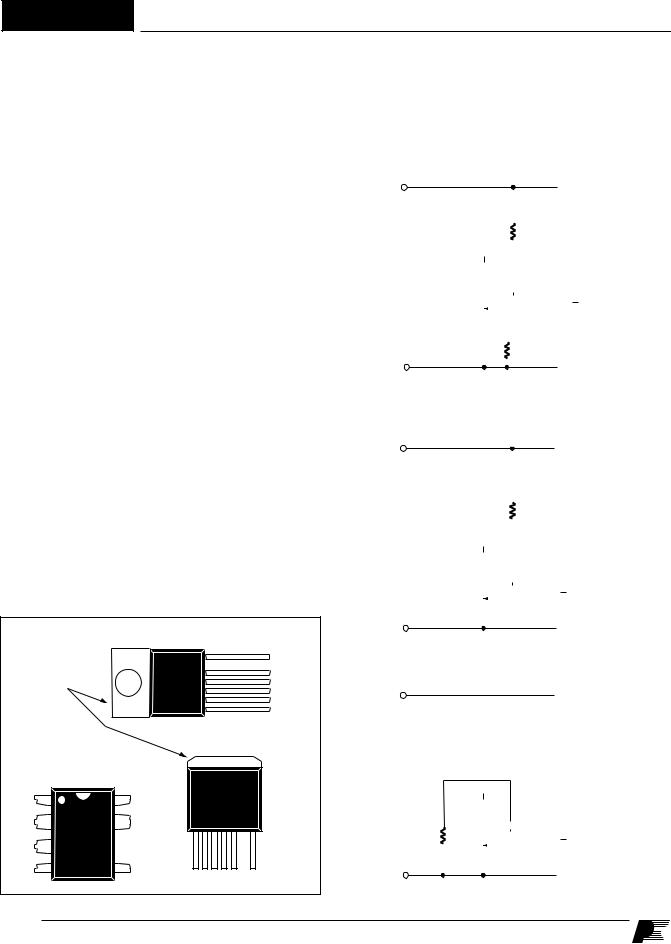
Y Package (TO-220-7C)
Tab Internally |
7 D |
Connected to |
5 F |
SOURCE Pin |
4 S |
|
3 X |
|
2 L |
|
1 C |
P Package (DIP-8B)
G Package (SMD-8B)
M |
1 |
8 |
S |
S |
2 |
7 |
S |
S |
3 |
|
|
C |
4 |
5 |
D |
R Package (TO-263-7C)
1 2 3 4 5 |
7 |
C L X S F |
D PI-2724-033001 |
Figure 3. Pin Configuration (top view).
connected to SOURCE pin and 66 kHz if connected to CONTROL pin. The switching frequency is internally set for fixed 132 kHz operation in P and G packages.
SOURCE (S) Pin:
Output MOSFET source connection for high voltage power return. Primary side control circuit common and reference point.
+ |
|
|
|
|
|
|
|
|
|
|
VUV = IUV x RLS |
|
|
|
|
|
|
|
|
|
|
|
|||
|
|
|
|
|
|
|
|
|
|
VOV = IOV x RLS |
||
|
|
|
|
|
|
|
|
|
|
|
||
|
|
|
|
|
For RLS = 2 MΩ |
|||||||
|
|
|
RLS 2 MΩ |
|||||||||
|
|
|
|
|
|
|
|
|
|
|
VUV = 100 VDC |
|
|
|
|
|
|
|
|
|
|
|
|
||
DC |
|
|
|
|
|
|
|
|
|
|
VOV = 450 VDC |
|
D |
|
|
|
|
|
|
L |
DCMAX@100 VDC = 78% |
||||
|
|
|
|
|
|
|||||||
Input |
|
|
|
|
|
|
||||||
|
|
|
|
|
|
|
|
|
|
DCMAX@375 VDC = 38% |
||
Voltage |
|
|
|
|
CONTROL |
|
||||||
|
|
|
|
|
C |
|
||||||
|
|
|
|
|
|
|
|
|
|
|
||
|
|
|
|
|
|
|
|
|
|
|
For RIL = 12 kΩ |
|
|
|
|
|
|
|
|
|
|
|
|
||
|
S |
|
|
|
|
|
X |
ILIMIT = 69% |
||||
|
|
|
|
|
|
|
|
RIL |
See fig. 55 for other |
|||
|
|
|
|
|
|
|
|
|||||
|
|
|
|
|
|
|
|
resistor values (RIL) |
||||
- |
|
|
|
|
|
|
12 kΩ |
|||||
|
|
|
|
|
|
to select different ILIMIT |
||||||
|
|
|
|
|
|
|
|
|
|
|
||
|
|
|
|
|
|
|
|
|
|
|
values PI-2629-040501 |
|
|
|
|
|
|
|
|
|
|
|
|
|
|
Figure 4. Y/R Package Line Sense and Externally Set Current
Limit.
+ |
|
|
|
|
|
|
|
|
|
|
|
|
|
|
|
|
|
|
|
|
|
|
|
|
|
|
|
|
|
|
|
|
|
|
|
|
|
VUV = IUV x RLS |
|
|
|
|
|
|
|
|
|
|
|
|
VOV = IOV x RLS |
|
|
|
|
RLS |
|
2 MΩ |
For RLS = 2 MΩ |
|||||
|
|
|
|
|
||||||||
|
|
|
|
|
|
VUV = 100 VDC |
||||||
DC |
|
|
|
|
|
|
|
|
|
|
|
|
|
|
|
|
|
|
|
|
|
|
|
VOV = 450 VDC |
|
Input |
|
|
|
|
|
|
|
|
|
|
|
|
|
|
|
|
|
|
|
|
|
|
|
|
|
Voltage |
D |
|
|
|
|
|
|
|
M |
DCMAX@100 VDC = 78% |
||
|
|
|
|
|
|
|
||||||
|
|
|
|
|
|
|
|
DCMAX@375 VDC = 38% |
||||
|
|
|
|
|
CONTROL |
C |
||||||
|
|
|
|
|
|
|
|
|
|
|
||
|
|
|
|
|
|
|
|
|
|
|
|
|
|
|
|
|
|
|
|
|
|
|
|
|
|
- |
S |
|
|
|
|
|
|
|
|
|||
|
|
|
|
|
|
|
|
|
|
|
|
|
|
|
|
|
|
|
|
|
|
|
|
|
PI-2509-040501 |
|
|
|
|
|
|
|
|
|
|
|
|
|
Figure 5. P/G Package Line Sense.
+ |
|
|
|
|
|
|
|
|
|
|
|
|
|
For RIL = 12 kΩ |
|
|
|
|
|
|
|
|
|
|
|
|
|
|
|
|
|
|
|
|
|
|
|
|
|
|
|
|
|
ILIMIT = 69% |
|
|
|
|
|
|
|
|
|
|
|
|
|
|
For RIL = 25 kΩ |
DC |
|
|
|
|
|
|
|
|
|
|
|
|
|
ILIMIT = 43% |
|
|
|
|
|
|
|
|
|
|
|
|
|
See fig. 55 for other |
|
Input |
|
|
|
|
|
|
|
|
|
|
|
|
|
|
|
|
|
|
|
|
|
|
|
|
|
|
|
resistor values (RIL) |
|
Voltage |
|
|
|
|
|
|
|
|
|
|
|
|
|
|
|
|
|
|
D |
|
|
|
|
M |
|
to select different |
|||
|
|
|
|
|
|
|
|
|
|
|||||
|
|
|
|
|
|
|
|
|
|
ILIMIT values |
||||
|
|
|
|
|
|
|
|
|
|
|
|
|
|
|
|
RIL |
|
|
|
|
|
|
|
CONTROL |
|
|
|||
|
|
|
|
|
|
|
|
|
C |
|||||
|
|
|
|
|
|
|
|
|
|
|
|
|||
|
|
|
|
|
|
|
|
|
|
|
|
|
|
|
|
|
|
|
|
|
|
|
|
|
|
|
|
|
|
- |
|
|
|
|
S |
|
|
|
|
|
|
|
|
|
|
|
|
|
|
|
|
|
|
|
|
|
|
|
|
|
|
|
|
|
|
|
|
|
|
|
|
|
|
PI-2517-040501 |
|
|
|
|
|
|
|
|
|
|
|
|
|
|
|
Figure 6. P/G Package Externally Set Current Limit.
4 |
E |
7/01 |
|
|
|
August 8, 2000

TOP242-249
TOPSwitch-GX Family Functional Description
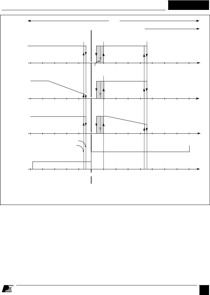
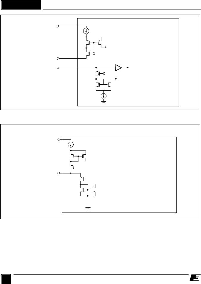
Like TOPSwitch, TOPSwitch-GX is an integrated switched mode power supply chip that converts a current at the control input to a duty cycle at the open drain output of a high voltage power MOSFET. During normal operation the duty cycle of the power MOSFET decreases linearly with increasing CONTROL pin current as shown in Figure 7.
In addition to the three terminal TOPSwitch features, such as the high voltage start-up, the cycle-by-cycle current limiting, loop compensation circuitry, auto-restart, thermal shutdown, the TOPSwitch-GX incorporates many additional functions that reduce system cost, increase power supply performance and design flexibility. A patented high voltage CMOS technology allows both the high voltage power MOSFET and all the low voltage control circuitry to be cost effectively integrated onto a single monolithic chip.
Three terminals, FREQUENCY, LINE-SENSE, and EXTERNAL CURRENT LIMIT (available in Y or R package) or one terminal MULTI-FUNCTION (available in P or G Package) have been added to implement some of the new functions. These terminals can be connected to the SOURCE pin to operate the TOPSwitch-GX in a TOPSwitch-like three terminal mode. However, even in this three terminal mode, the TOPSwitch-GX offers many new transparent features that do not require any external components:
1.A fully integrated 10 ms soft-start limits peak currents and voltages during start-up and dramatically reduces or eliminates output overshoot in most applications.
2.DCMAX of 78% allows smaller input storage capacitor, lower input voltage requirement and/or higher power capability.
3.Frequency reduction at light loads lowers the switching losses and maintains good cross regulation in multiple output supplies.
4.Higher switching frequency of 132 kHz reduces the transformer size with no noticeable impact on EMI.
5.Frequency jittering reduces EMI.
6.Hysteretic over-temperature shutdown ensures automatic recovery from thermal fault. Large hysteresis prevents circuit board overheating.
7.Packages with omitted pins and lead forming provide large drain creepage distance.
8.Tighter absolute tolerances and smaller temperature variations on switching frequency, current limit and PWM gain.
The LINE-SENSE (L) pin is usually used for line sensing by connecting a resistor from this pin to the rectified DC high voltage bus to implement line overvoltage (OV), under-voltage (UV) and line feed forward with DCMAX reduction. In this mode, the value of the resistor determines the OV/UV thresholds and the DCMAX is reduced linearly starting from a line voltage above the under-voltage threshold. See Table 2 and Figure 11.
Auto-restart
|
ICD1 |
IB |
|
|
IL = 125 A |
|
132 |
|
(kHz) |
|
IL < IL(DC) |
|
IL = 190 A |
|
Frequency |
30 |
|
|
|
|
|
|
IC (mA) |
Auto-restart
|
ICD1 |
|
IB |
|
|
78 |
|
Slope = PWM Gain |
|
|
|
|
|
|
(%) |
|
|
|
|
Cycle |
38 |
|
IL = 125 A |
|
|
|
|
||
Duty |
|
|
IL < IL(DC) |
|
|
IL = 190 A |
|
||
|
10 |
|
|
|
|
TOP242/5 1.6 |
2.0 |
5.2 |
6.0 |
|
TOP246/9 2.2 |
2.6 |
5.8 |
6.6 |
|
|
|
IC (mA) |
|
Note: For P and G packages IL is replaced with IM.
PI-2633-060500
Figure 7. Relationship of Duty Cycle and Frequency to CONTROL Pin Current.
The pin can also be used as a remote ON/OFF and a synchronization input.
The EXTERNAL CURRENT LIMIT (X) pin is usually used to reduce the current limit externally to a value close to the operating peak current, by connecting the pin to SOURCE through a resistor. This pin can also be used as a remote ON/OFF and a synchronization input in both modes. See Table 2 and Figure 11.
For the P or G packages the LINE-SENSE and EXTERNAL CURRENT LIMIT pin functions are combined on one MULTIFUNCTION (M) pin. However, some of the functions become mutually exclusive as shown in Table 3.
The FREQUENCY (F) pin in the Y or R package sets the switching frequency to the default value of 132 kHz when connected to SOURCE pin. A half frequency option of 66 kHz can be chosen by connecting this pin to CONTROL pin instead. Leaving this pin open is not recommended.
August 8, 2000
E 5 7/01
TOP242-249
CONTROL (C) Pin Operation
The CONTROL pin is a low impedance node that is capable of receiving a combined supply and feedback current. During normal operation, a shunt regulator is used to separate the feedback signal from the supply current. CONTROL pin voltage VC is the supply voltage for the control circuitry including the MOSFET gate driver. An external bypass capacitor closely connected between the CONTROL and SOURCE pins is required to supply the instantaneous gate drive current. The total amount of capacitance connected to this pin also sets the auto-restart timing as well as control loop compensation.
When rectified DC high voltage is applied to the DRAIN pin during start-up, the MOSFET is initially off, and the CONTROL pin capacitor is charged through a switched high voltage current source connected internally between the DRAIN and CONTROL pins. When the CONTROL pin voltage VC reaches approximately 5.8 V, the control circuitry is activated and the soft-start begins. The soft-start circuit gradually increases the duty cycle of the MOSFET from zero to the maximum value over approximately 10 ms. If no external feedback/supply current is fed into the CONTROL pin by the end of the soft-start, the high voltage current source is turned off and the CONTROL pin will start discharging in response to the supply current drawn by the control circuitry. If the power supply is designed properly, and no fault condition such as open loop or shorted output exists, the feedback loop will close, providing external CONTROL pin current, before the CONTROL pin voltage has had a chance to discharge to the lower threshold voltage of approximately 4.8 V (internal supply under-voltage lockout threshold). When the externally fed current charges the CONTROL pin to the shunt regulator voltage of 5.8 V, current
in excess of the consumption of the chip is shunted to SOURCE through resistor RE as shown in Figure 2. This current flowing through RE controls the duty cycle of the power MOSFET to provide closed loop regulation. The shunt regulator has a finite low output impedance ZC that sets the gain of the error amplifier when used in a primary feedback configuration. The dynamic impedance ZC of the CONTROL pin together with the external CONTROL pin capacitance sets the dominant pole for the control loop.
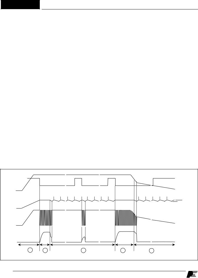
When a fault condition such as an open loop or shorted output prevents the flow of an external current into the CONTROL pin, the capacitor on the CONTROL pin discharges towards 4.8 V. At 4.8 V, auto-restart is activated which turns the output MOSFET off and puts the control circuitry in a low current standby mode. The high-voltage current source turns on and charges the external capacitance again. A hysteretic internal supply under-voltage comparator keeps VC within a window of typically 4.8 to 5.8 V by turning the high-voltage current source on and off as shown in Figure 8. The auto-restart circuit has a divide-by-8 counter which prevents the output MOSFET from turning on again until eight discharge/charge cycles have elapsed. This is accomplished by enabling the output MOSFET only when the divide-by-8 counter reaches full count (S7). The counter effectively limits TOPSwitch-GX power dissipation by reducing the auto-restart duty cycle to typically 4%. Autorestart mode continues until output voltage regulation is again achieved through closure of the feedback loop.
Oscillator and Switching Frequency
The internal oscillator linearly charges and discharges an internal capacitance between two voltage levels to create a sawtooth
|
|
|
~ |
|
|
|
|
~ |
|
|
|
|
|
|
|
|
|
VUV |
|
|
|
|
|
|
|
|
|
|
|
|
|
|
|
|
|
VLINE |
|
|
~ |
|
|
|
|
~ |
|
|
|
|
~ |
|
|
|
|
0 V |
|
|
|
|
|
|
|
|
|
|
|
|
|
|
|
|
|
S7 |
S0 |
S1 |
S2 |
S6 |
S7 |
S0 |
S1 |
S2 |
S6 |
S7 |
S0 |
S1 |
S2 |
S6 |
S7 |
S7 |
5.8 V |
VC |
|
|
~ |
|
|
|
|
~ |
|
|
|
|
~ |
|
|
|
4.8 V |
|
|
|
|
|
|
|
|
|
|
|
|
|
|
|
|
||
0 V |
|
|
~ |
|
|
|
|
~ |
|
|
|
|
|
|
|
|
|
|
|
|
|
|
|
|
|
|
|
|
|
|
|
|
|
||
VDRAIN |
|
|
|
|
|
|
|
|
|
|
|
|
~ |
|
|
|
|
0 V |
|
|
|
|
|
|
|
|
|
|
|
|
|
|
|
|
|
VOUT |
|
|
|
|
|
|
|
|
|
|
|
|
|
|
|
|
|
0 V |
|
|
~ |
|
|
|
|
~ |
|
|
|
|
~ |
|
|
|
|
1 |
2 |
|
|
|
|
3 |
|
|
|
|
2 |
|
4 |
|
|
|
|
Note: S0 through S7 are the output states of the auto-restart counter |
|
|
|
|
|
|
|
|
PI-2545-082299 |
||||||||
|
|
|
|
|
|
|
|
|
|
|
|
|
|
|
|
|
|
Figure 8. Typical Waveforms for (1) Power Up (2) Normal Operation (3) Auto-restart (4) Power Down.
6 |
E |
7/01 |
|
|
|
August 8, 2000
waveform for the pulse width modulator. This oscillator sets the pulse width modulator/current limit latch at the beginning of each cycle.
The nominal switching frequency of 132 kHz was chosen to minimize transformer size while keeping the fundamental EMI frequency below 150 kHz. The FREQUENCY pin (available only in Y or R package), when shorted to the CONTROL pin, lowers the switching frequency to 66 kHz (half frequency) which may be preferable in some cases such as noise sensitive video applications or a high efficiency standby mode. Otherwise, the FREQUENCY pin should be connected to the SOURCE pin for the default 132 kHz.
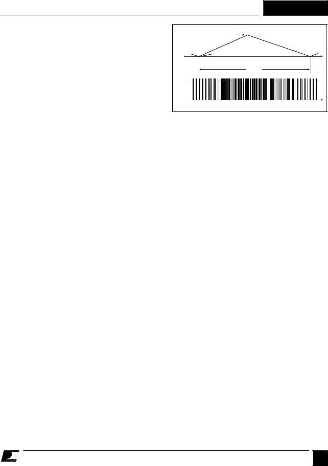
To further reduce the EMI level, the switching frequency is jittered (frequency modulated) by approximately ±4 kHz at 250 Hz (typical) rate as shown in Figure 9. Figure 46 shows the typical improvement of EMI measurements with frequency jitter.
Pulse Width Modulator and Maximum Duty Cycle
The pulse width modulator implements voltage mode control by driving the output MOSFET with a duty cycle inversely proportional to the current into the CONTROL pin that is in excess of the internal supply current of the chip (see Figure 7). The excess current is the feedback error signal that appears across RE (see Figure 2). This signal is filtered by an RC network with a typical corner frequency of 7 kHz to reduce the effect of switching noise in the chip supply current generated by the MOSFET gate driver. The filtered error signal is compared with the internal oscillator sawtooth waveform to generate the duty cycle waveform. As the control current increases, the duty cycle decreases. A clock signal from the oscillator sets a latch which turns on the output MOSFET. The pulse width modulator resets the latch, turning off the output MOSFET. Note that a minimum current must be driven into the CONTROL pin before the duty cycle begins to change.
The maximum duty cycle, DCMAX, is set at a default maximum value of 78% (typical). However, by connecting the LINESENSE or MULTI-FUNCTION pin (depending on the package) to the rectified DC high voltage bus through a resistor with appropriate value, the maximum duty cycle can be made to decrease from 78% to 38% (typical) as shown in Figure 11 when input line voltage increases (see line feed forward with DCMAX reduction).
Light Load Frequency Reduction
The pulse width modulator duty cycle reduces as the load at the power supply output decreases. This reduction in duty cycle is proportional to the current flowing into the CONTROL pin. As the CONTROL pin current increases, the duty cycle decreases linearly towards a duty cycle of 10%. Below 10% duty cycle, to maintain high efficiency at light loads, the frequency is also reduced linearly until a minimum frequency is reached at a duty
|
TOP242-249 |
136 kHz |
-092499 |
Switching |
PI-2550 |
Frequency |
|
128 kHz |
|
|
4 ms |
VDRAIN |
|
|
Time |
Figure 9. Switching Frequency Jitter. (Idealized VDRAIN waveform)
cycle of 0% (refer to Figure 7). The minimum frequency is typically 30 kHz and 15 kHz for 132 kHz and 66 kHz operation, respectively.
This feature allows a power supply to operate at lower frequency at light loads thus lowering the switching losses while maintaining good cross regulation performance and low output ripple.
Error Amplifier
The shunt regulator can also perform the function of an error amplifier in primary side feedback applications. The shunt regulator voltage is accurately derived from a temperaturecompensated bandgap reference. The gain of the error amplifier is set by the CONTROL pin dynamic impedance. The CONTROL pin clamps external circuit signals to the VC voltage level. The CONTROL pin current in excess of the supply current is separated by the shunt regulator and flows through RE as a voltage error signal.
On-chip Current Limit with External Programmability
The cycle-by-cycle peak drain current limit circuit uses the output MOSFET ON-resistance as a sense resistor. A current limit comparator compares the output MOSFET on-state drain
to source voltage, VDS(ON) with a threshold voltage. High drain current causes VDS(ON) to exceed the threshold voltage and turns the output MOSFET off until the start of the next clock cycle.
The current limit comparator threshold voltage is temperature compensated to minimize the variation of the current limit due
to temperature related changes in RDS(ON) of the output MOSFET. The default current limit of TOPSwitch-GX is preset internally.
However, with a resistor connected between EXTERNAL CURRENT LIMIT (X) pin (Y or R package) or MULTIFUNCTION (M) pin (P or G package) and SOURCE pin, current limit can be programmed externally to a lower level between 30% and 100% of the default current limit. Please refer to the graphs in the typical performance characteristics section for the selection of the resistor value. By setting current limit low, a larger TOPSwitch-GX than necessary for the power
required can be used to take advantage of the lower RDS(ON) for higher efficiency/smaller heat sinking requirements. With a
August 8, 2000
E 7 7/01
TOP242-249
second resistor connected between the EXTERNAL CURRENT LIMIT (X) pin (Y or R package) or MULTI-FUNCTION (M) pin (P or G package) and the rectified DC high voltage bus, the current limit is reduced with increasing line voltage, allowing a true power limiting operation against line variation to be implemented. When using an RCD clamp, this power limiting technique reduces maximum clamp voltage at high line. This allows for higher reflected voltage designs as well as reducing clamp dissipation.
The leading edge blanking circuit inhibits the current limit comparator for a short time after the output MOSFET is turned on. The leading edge blanking time has been set so that, if a power supply is designed properly, current spikes caused by primary-side capacitances and secondary-side rectifier reverse recovery time should not cause premature termination of the switching pulse.
The current limit is lower for a short period after the leading edge blanking time as shown in Figure 52. This is due to dynamic characteristics of the MOSFET. To avoid triggering the current limit in normal operation, the drain current waveform should stay within the envelope shown.
Line Under-Voltage Detection (UV)
At power up, UV keeps TOPSwitch-GX off until the input line voltage reaches the under voltage threshold. At power down, UV prevents auto-restart attempts after the output goes out of regulation. This eliminates power down glitches caused by the slow discharge of large input storage capacitor present in applications such as standby supplies. A single resistor connected from the LINE-SENSE pin (Y or R package) or MULTIFUNCTION pin (P or G package) to the rectified DC high voltage bus sets UV threshold during power up. Once the power supply is successfully turned on, the UV threshold is lowered to
40% of the initial UV threshold to allow extended input voltage operating range (UV low threshold). If the UV low threshold is reached during operation without the power supply losing regulation the device will turn off and stay off until UV (high threshold) has been reached again. If the power supply loses regulation before reaching the UV low threshold, the device will enter auto-restart. At the end of each auto-restart cycle (S7), the UV comparator is enabled. If the UV high threshold is not exceeded the MOSFET will be disabled during the next cycle (see figure 8). The UV feature can be disabled independent of OV feature as shown in Figure 19 and 23.
Line Overvoltage Shutdown (OV)
The same resistor used for UV also sets an overvoltage threshold which, once exceeded, will force TOPSwitch-GX output into off-state. The ratio of OV and UV thresholds is preset at 4.5 as can be seen in Figure 11. When the MOSFET is off, the rectified DC high voltage surge capability is increased to the voltage rating of the MOSFET (700 V), due to the absence of the reflected voltage and leakage spikes on the drain. A small amount of hysteresis is provided on the OV threshold to prevent noise triggering. The OV feature can be disabled independent of the UV feature as shown in Figure 18 and 32.
Line Feed Forward with DCMAX Reduction
The same resistor used for UV and OV also implements line voltage feed forward which minimizes output line ripple and reduces power supply output sensitivity to line transients. This feed forward operation is illustrated in Figure 7 by the different values of IL (Y or R package) or IM (P or G Package). Note that for the same CONTROL pin current, higher line voltage results in smaller operating duty cycle. As an added feature, the maximum duty cycle DCMAX is also reduced from 78% (typical) at a voltage slightly higher than the UV threshold to 38% (typical) at the OV threshold (see Figures 7, 11). Limiting
Oscillator
(SAW)
DMAX
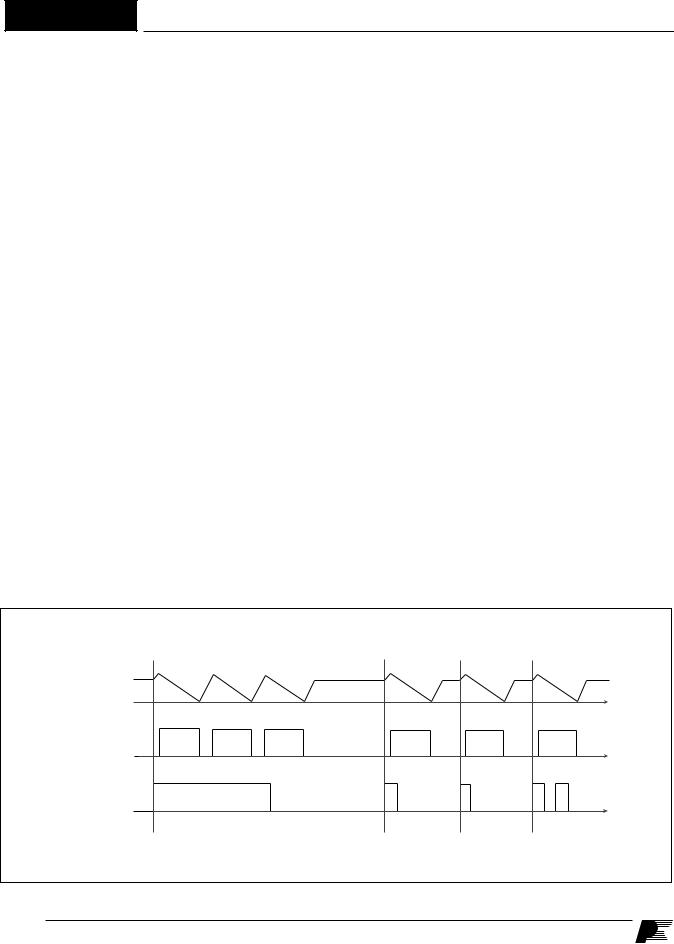
Enable from X, L or M Pin (STOP)
Time
PI-2637-060600
Figure 10. Synchronization Timing Diagram.
8 |
E |
7/01 |
|
|
|
August 8, 2000

DCMAX at higher line voltages helps prevent transformer saturation due to large load transients in forward converter applications. DCMAX of 38% at the OV threshold was chosen to ensure that the power capability of the TOPSwitch-GX is not restricted by this feature under normal operation.
Remote ON/OFF and Synchronization
TOPSwitch-GX can be turned on or off by controlling the current into the LINE-SENSE pin or out from the EXTERNAL CURRENT LIMIT pin (Y or R package) and into or out from the MULTI-FUNCTION pin (P or G package) (see Figure 11). In addition, the LINE-SENSE pin has a 1 V threshold comparator connected at its input. This voltage threshold can also be used to perform remote ON/OFF control. This allows easy implementation of remote ON/OFF control of TOPSwitch-GX in several different ways. A transistor or an optocoupler output connected between the EXTERNAL CURRENT LIMIT or LINE-SENSE pins (Y or R package) or the MULTI-FUNCTION pin (P or G package) and the SOURCE pin implements this function with “active-on” (Figure 22, 29 and 36) while a transistor or an optocoupler output connected between the LINE-SENSE pin (Y or R package) or the MULTI-FUNCTION (P or G package) pin and the CONTROL pin implements the function with “active-off” (Figure 23 and 37).
When a signal is received at the LINE-SENSE pin or the EXTERNAL CURRENT LIMIT pin (Y or R package) or the MULTI-FUNCTION pin (P or G package) to disable the output through any of the pin functions such as OV, UV and remote ON/OFF, TOPSwitch-GXalways completes its current switching cycle, as illustrated in Figure 10, before the output is forced off. The internal oscillator is stopped slightly before the end of the current cycle and stays there as long as the disable signal exists. When the signal at the above pins changes state from disable to enable, the internal oscillator starts the next switching cycle. This approach allows the use of this pin to synchronize TOPSwitch-GX to any external signal with a frequency lower than its internal switching frequency.
As seen above, the remote ON/OFF feature allows the TOPSwitch-GX to be turned on and off instantly, on a cycle-by- cycle basis, with very little delay. However, remote ON/OFF can also be used as a standby or power switch to turn off the TOPSwitch-GX and keep it in a very low power consumption state for indefinitely long periods. If the TOPSwitch-GX is held in remote off state for long enough time to allow the CONTROL pin to dishcharge to the internal supply under-voltage threshold of 4.8 V (approximately 32 ms for a 47 F CONTROL pin capacitance), the CONTROL pin goes into the hysteretic mode of regulation. In this mode, the CONTROL pin goes through alternate charge and discharge cycles between 4.8 V and 5.8 V (see CONTROL pin operation section above) and runs entirely off the high voltage DC input, but with very low power consumption (160 mW typical at 230 VAC with M or X pins
TOP242-249
open). When the TOPSwitch-GX is remotely turned on after entering this mode, it will initiate a normal start-up sequence with soft-start the next time the CONTROL pin reaches 5.8 V. In the worst case, the delay from remote on to start-up can be equal to the full discharge/charge cycle time of the CONTROL pin, which is approximately 125 ms for a 47 F CONTROL pin capacitor. This reduced consumption remote off mode can eliminate expensive and unreliable in-line mechanical switches. It also allows for microprocessor controlled turn-on and turnoff sequences that may be required in certain applications such as inkjet and laser printers.
Soft-Start
Two on-chip soft-start functions are activated at start-up with a duration of 10 ms (typical). Maximum duty cycle starts from 0% and linearly increases to the default maximum of 78% at the end of the 10 ms duration and the current limit starts from about 85% and linearly increases to 100% at the end of the 10ms duration. In addition to start-up, soft-start is also activated at each restart attempt during auto-restart and when restarting after being in hysteretic regulation of CONTROL pin voltage (VC), due to remote off or thermal shutdown conditions. This effectively minimizes current and voltage stresses on the output MOSFET, the clamp circuit and the output rectifier during startup. This feature also helps minimize output overshoot and prevents saturation of the transformer during start-up.
Shutdown/Auto-Restart
To minimize TOPSwitch-GX power dissipation under fault conditions, the shutdown/auto-restart circuit turns the power supply on and off at an auto-restart duty cycle of typically 4% if an out of regulation condition persists. Loss of regulation interrupts the external current into the CONTROL pin. VC regulation changes from shunt mode to the hysteretic autorestart mode as described in CONTROL pin operation section. When the fault condition is removed, the power supply output becomes regulated, VC regulation returns to shunt mode, and normal operation of the power supply resumes.
Hysteretic Over-Temperature Protection
Temperature protection is provided by a precision analog circuit that turns the output MOSFET off when the junction temperature exceeds the thermal shutdown temperature (140 °C typical). When the junction temperature cools to below the hysteretic temperature, normal operation resumes providing automatic recovery. A large hysteresis of 70 °C (typical) is provided to prevent overheating of the PC board due to a continuous fault condition. VC is regulated in hysteretic mode and a 4.8 V to 5.8 V (typical) sawtooth waveform is present on the CONTROL pin while in thermal shutdown.
Bandgap Reference
All critical TOPSwitch-GX internal voltages are derived from a temperature-compensated bandgap reference. This reference is
August 8, 2000
E 9 7/01

TOP242-249
also used to generate a temperature-compensated current reference which is trimmed to accurately set the switching frequency, MOSFET gate drive current, current limit, and the line OV/UV thresholds. TOPSwitch-GX has improved circuitry to maintain all of the above critical parameters within very tight absolute and temperature tolerances.
High-Voltage Bias Current Source
This current source biases TOPSwitch-GX from the DRAIN pin and charges the CONTROL pin external capacitance during start-up or hysteretic operation. Hysteretic operation occurs during auto-restart, remote off and over-temperature shutdown. In this mode of operation, the current source is switched on and off with an effective duty cycle of approximately 35%. This duty cycle is determined by the ratio of CONTROL pin charge (IC) and discharge currents (ICD1 and ICD2). This current source is turned off during normal operation when the output MOSFET is switching. The effect of the current source switching will be seen on the DRAIN voltage waveform as small disturbances and is normal.
10 E7/01
August 8, 2000
Using Feature Pins
FREQUENCY (F) Pin Operation
The FREQUENCY pin is a digital input pin available in the Y or R package only. Shorting the FREQUENCY pin to SOURCE pin selects the nominal switching frequency of 132 kHz (Figure 13) which is suited for most applications. For other cases that may benefit from lower switching frequency such as noise sensitive video applications, a 66 kHz switching frequency (half frequency) can be selected by shorting the FREQUENCY pin to the CONTROL pin (Figure 14). In addition, an example circuit shown in Figure 15 may be used to lower the switching frequency from 132 kHz in normal operation to 66 kHz in standby mode for very low standby power consumption.
LINE-SENSE (L) Pin Operation (Y and R Packages)
When current is fed into the LINE-SENSE pin, it works as a voltage source of approximately 2.6 V up to a maximum current of +400 A (typical). At +400 A, this pin turns into a constant current sink. Refer to Figure 12a. In addition, a comparator with a threshold of 1 V is connected at the pin and is used to detect when the pin is shorted to the SOURCE pin.
There are a total of four functions available through the use of the LINE-SENSE pin: OV, UV, line feed forward with DCMAX reduction, and remote ON/OFF. Connecting the LINE-SENSE pin to the SOURCE pin disables all four functions. The LINESENSE pin is typically used for line sensing by connecting a resistor from this pin to the rectified DC high voltage bus to implement OV, UV and DCMAX reduction with line voltage. In this mode, the value of the resistor determines the line OV/UV thresholds, and the DCMAX is reduced linearly with rectified DC high voltage starting from just above the UV threshold. The pin can also be used as a remote on/off and a synchronization input.
TOP242-249
Refer to Table 2 for possible combinations of the functions with example circuits shown in Figure 16 through Figure 40. A description of specific functions in terms of the LINE-SENSE pin I/V characteristic is shown in Figure 11 (right hand side). The horizontal axis represents LINE-SENSE pin current with positive polarity indicating currents flowing into the pin. The meaning of the vertical axes varies with functions. For those that control the on/off states of the output such as UV, OV and remote ON/OFF, the vertical axis represents the enable/disable states of the output. UV triggers at IUV (+50 A typical with 30 A hysteresis) and OV triggers at IOV (+225 A typical with 8 A hysteresis). Between the UV and OV thresholds, the output is enabled. For line feed forward with DCMAX reduction, the vertical axis represents the magnitude of the DCMAX. Line feed forward with DCMAX reduction lowers maximum duty cycle from 78% at IL(DC) (+60 A typical) to 38% at IOV (+225 A).
EXTERNAL CURRENT LIMIT (X) Pin Operation (Y and R Packages)
When current is drawn out of the EXTERNAL CURRENT LIMIT pin, it works as a voltage source of approximately 1.3 V up to a maximum current of –240 A (typical). At –240 A, it turns into a constant current source (refer to Figure 12a).
There are two functions available through the use of the EXTERNAL CURRENT LIMIT pin: external current limit and remote ON/OFF. Connecting the EXTERNAL CURRENT LIMIT pin and SOURCE pin disables the two functions. In high efficiency applications this pin can be used to reduce the current limit externally to a value close to the operating peak current, by connecting the pin to the SOURCE pin through a resistor. The pin can also be used as a remote on/off. Table 2 shows several possible combinations using this pin. See Figure
LINE-SENSE AND EXTERNAL CURRENT LIMIT PIN TABLE*
Figure Number |
▲ |
Three Terminal Operation
Under-Voltage
Overvoltage
Line Feed Forward (DCMAX)
Overload Power Limiting
External Current Limit
Remote ON/OFF
16 |
17 |
18 |
19 |
20 |
21 |
22 |
23 |
24 |
25 |
26 |
27 |
28 |
29 |
|
|
|
|
|
|
|
|
|
|
|
|
|
|
|
|
|
|
|
|
|
|
|
|
|
|
|
|
|
|
|
|
|
|
|
|
|
|
|
|
|
|
|
|
|
|
|
|
|
|
|
|
|
|
|
|
|
|
|
|
|
|
|
|
|
|
|
|
|
|
|
|
|
|
|
|
|
|
|
|
|
|
|
|
|
|
|
|
|
|
|
|
|
|
|
|
|
|
|
|
|
|
|
|
|
|
|
|
|
|
|
|
*This table is only a partial list of many LINE-SENSE and EXTERNAL CURRENT LIMIT pin configurations that are possible.
Table 2. Typical LINE-SENSE and EXTERNAL CURRENT LIMIT Pin Configurations.
August 8, 2000
7/01E 11

TOP242-249
MULTI-FUNCTION PIN TABLE*
Figure Number ▲ |
30 |
31 |
32 |
33 |
34 |
35 |
36 |
37 |
38 |
39 |
40 |
|
|
|
|
|
|
|
|
|
|
|
|
Three Terminal Operation |
|
|
|
|
|
|
|
|
|
|
|
|
|
|
|
|
|
|
|
|
|
|
|
Under-Voltage |
|
|
|
|
|
|
|
|
|
|
|
|
|
|
|
|
|
|
|
|
|
|
|
Overvoltage |
|
|
|
|
|
|
|
|
|
|
|
|
|
|
|
|
|
|
|
|
|
|
|
Line Feed Forward (DCMAX) |
|
|
|
|
|
|
|
|
|
|
|
Overload Power Limiting |
|
|
|
|
|
|
|
|
|
|
|
|
|
|
|
|
|
|
|
|
|
|
|
External Current Limit |
|
|
|
|
|
|
|
|
|
|
|
|
|
|
|
|
|
|
|
|
|
|
|
Remote ON/OFF |
|
|
|
|
|
|
|
|
|
|
|
|
|
|
|
|
|
|
|
|
|
|
|
*This table is only a partial list of many MULTI-FUNCTION pin configurations that are possible.
Table 3. Typical MULTI-FUNCTION Pin Configurations.
11 for a description of the functions where the horizontal axis (left hand side) represents the EXTERNAL CURRENT LIMIT pin current. The meaning of the vertical axes varies with function. For those that control the on/off states of the output such as remote ON/OFF, the vertical axis represents the enable/ disable states of the output. For external current limit, the vertical axis represents the magnitude of the ILIMIT. Please see graphs in the typical performance characteristics section for the current limit programming range and the selection of appropriate resistor value.
MULTI-FUNCTION(M)PinOperation(PandGPackages)
The LINE-SENSE and EXTERNAL CURRENT LIMIT pin functions are combined to a single MULTI-FUNCTION pin for P and G packages. The comparator with a 1 V threshold at the LINE-SENSE pin is removed in this case as shown in Figure 2b. All of the other functions are kept intact. However, since some of the functions require opposite polarity of input current (MULTI-FUNCTION pin), they are mutually exclusive. For example, line sensing features cannot be used simultaneously with external current limit setting. When current is fed into the MULTI-FUNCTION pin, it works as a voltage source of approximately 2.6 V up to a maximum current of +400 A (typical). At +400 A, this pin turns into a constant current sink. When current is drawn out of the MULTI-FUNCTION pin, it works as a voltage source of approximately 1.3 V up to a maximum current of –240 A (typical). At –240 A, it turns into a constant current source. Refer to Figure 12b.
There are a total of five functions available through the use of the MULTI-FUNCTION pin: OV, UV, line feed forward with DCMAX reduction, external current limit and remote ON/OFF. A short circuit between the MULTI-FUNCTION pin and SOURCE pin disables all five functions and forces
TOPSwitch-GX to operate in a simple three terminal mode like TOPSwitch-II. The MULTI-FUNCTION pin is typically used for line sensing by connecting a resistor from this pin to the rectified DC high voltage bus to implement OV, UV and DCMAX reduction with line voltage. In this mode, the value of the resistor determines the line OV/UV thresholds, and the DCMAX is reduced linearly with rectified DC high voltage starting from just above the UV threshold. In high efficiency applications this pin can be used in the external current limit mode instead, to reduce the current limit externally to a value close to the operating peak current, by connecting the pin to the SOURCE pin through a resistor. The same pin can also be used as a remote on/off and a synchronization input in both modes. Please refer to Table 3 for possible combinations of the functions with example circuits shown in Figure 30 through Figure 40. A description of specific functions in terms of the MULTIFUNCTION pin I/V characteristic is shown in Figure 11. The horizontal axis represents MULTI-FUNCTION pin current with positive polarity indicating currents flowing into the pin. The meaning of the vertical axes varies with functions. For those that control the on/off states of the output such as UV, OV and remote ON/OFF, the vertical axis represents the enable/ disable states of the output. UV triggers at IUV (+50 A typical) and OV triggers at IOV (+225 A typical with 30 A hysteresis). Between the UV and OV thresholds, the output is enabled. For external current limit and line feed forward with DCMAX reduction, the vertical axis represents the magnitude of the ILIMIT and DCMAX. Line feed forward with DCMAX reduction lowers
maximum duty cycle from 78% at IM(DC) (+60 A typical) to 38% at IOV (+225 A). External current limit is available only with
negative MULTI-FUNCTION pin current. Please see graphs in the typical performance characteristics section for the current limit programming range and the selection of appropriate resistor value.
12 E7/01
August 8, 2000
TOP242-249
M Pin
 X Pin
X Pin 
 L Pin
L Pin
IREM(N) |
IUV |
IOV |
(Enabled)
Output
MOSFET
Switching
(Disabled)
Disabled when supply |
I |
output goes out of |
|
regulation |
|
ILIMIT (Default)
Current
Limit
I
DCMAX (78.5%)
Maximum
Duty Cycle
|
|
|
-22 A |
|
|
|
|
|
|
|
|
|
I |
|
|
|
|
|
|
|
|
|
|
|
|
|
|
||
|
|
|
-27 A |
|
|
|
VBG + VTP |
|
|
|
|
|
|
|
|
|
|
|
|
|
|
|
|
|
|
|
|
||
|
|
VBG |
|
|
|
|
|
|
|
|
|
|
|
|
Pin Voltage |
|
|
|
|
|
|
|
|
|
|
|
|
|
|
-250 |
-200 |
-150 |
-100 |
-50 |
0 |
50 |
100 |
150 |
200 |
250 |
300 |
350 |
400 |
I |
|
||||||||||||||
X and L Pins (Y or R Package) and M Pin (P or G Package) Current ( A)
Note: This figure provides idealized functional characteristics with typical performance values. Please refer to the parametric table and typical performance characteristics sections of the data sheet for measured data.
PI-2636-040501
Figure 11. MULTI-FUNCTION (P or G package), LINE-SENSE, and EXTERNAL CURRENT LIMIT (Y or R package) Pin Characteristics.
August 8, 2000
7/01E 13
TOP242-249
CONTROL Pin |
Y and R Package |
|
TOPSwitch-GX |
||
|
||
|
240 A |
|
|
(Negative Current Sense - ON/OFF, |
|
|
Current Limit Adjustment) |
|
EXTERNAL CURRENT LIMIT (X) |
VBG + VT |
|
|
(Voltage Sense) |
|
LINE-SENSE (L) |
1 V |
|
|
VBG |
|
|
(Positive Current Sense - Under-Voltage, |
|
|
Overvoltage, ON/OFF Maximum Duty |
|
|
Cycle Reduction) |
|
|
400 A |
PI-2634-033001
Figure 12a. LINE-SENSE (L), and EXTERNAL CURRENT LIMIT (X) Pin Input Simplified Schematic.
P and G Package
CONTROL Pin
TOPSwitch-GX
240 A
 (Negative Current Sense - ON/OFF,
Current Limit Adjustment)


 VBG + VT
MULTI-FUNCTION (M)

 VBG
VBG
 (Positive Current Sense - Under-Voltage,
Overvoltage, Maximum Duty
Cycle Reduction)
 400 A
400 A
PI-2548-092399
Figure 12b. MULTI-FUNCTION (M) Pin Input Simplified Schematic.
14 E7/01
August 8, 2000
TOP242-249
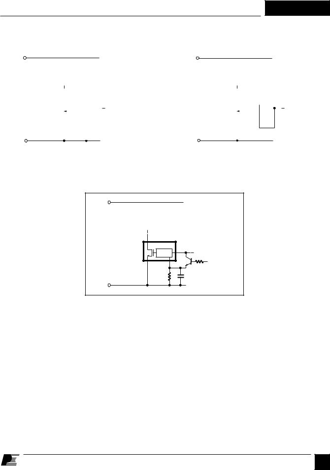
Typical Uses of FREQUENCY (F) Pin
+ |
|
|
|
|
|
|
|
|
|
|
|
|
|
+ |
|
|
|
|
|
|
|
|
|
|
DC |
D |
|
|
|
|
|
|
|
|
|
|
|
|
DC |
D |
|
|
|
|
|
|
|
|
|
|
|
|
|
|
|
|
|
|
|
|
|
|
|
|
|
|
|
|
|
|
||||
Input |
|
|
|
|
|
|
|
|
|
|
|
|
Input |
|
|
|
|
|
|
|
|
|
||
Voltage |
|
|
|
|
CONTROL |
|
C |
|
|
Voltage |
|
|
|
|
CONTROL |
|
C |
|||||||
|
|
|
|
|
|
|
|
|
|
|
|
|
|
|
|
|
|
|
|
|
||||
|
|
|
|
|
|
|
|
|
|
|
|
|
|
|
|
|
|
|
|
|
|
|
|
|
|
|
|
|
|
|
|
|
|
|
|
|
|
|
|
|
|
|
|
|
|
|
|
|
|
|
S |
|
|
|
|
|
F |
|
|
|
S |
|
|
|
|
F |
||||||||
- |
|
|
|
|
|
|
|
|
|
|
|
|
|
- |
|
|
|
|
|
|
|
|
|
|
|
|
|
|
|
|
|
|
|
|
|
|
PI-2654-071700 |
|
|
|
|
|
|
|
|
|
|
|
PI-2655-071700 |
|
|
|
|
|
|
|
|
|
|
|
|
|
|
|
|
|
|
|
|
|
|
|
|
|
Figure 13. Full Frequency Operation (132 kHz). |
|
Figure 14. Half Frequency Operation (66 kHz). |
||||||||||||||||||||||
+
|
|
QS can be an optocoupler output. |
||
DC |
D |
|
|
|
Input |
|
|
|
|
|
CONTROL |
|
|
|
Voltage |
|
C |
|
|
|
|
|
|
|
|
S |
F |
|
STANDBY |
|
QS |
47 kΩ |
||
|
|
RHF |
||
|
|
1 nF |
|
|
- |
|
20 kΩ |
|
|
|
|
|
||
|
|
|
|
|
|
|
|
|
PI-2656-040501 |
Figure 15. Half Frequency Standby Mode (For High Standby
Efficiency).
August 8, 2000
7/01E 15
 Loading...