


PI-2632-060200
AC
IN
DC
OUT
D
S
C
TOPSwitch-GX
CONTROL
L
+
-
FX
查询TOP250Y/F供应商查询TOP250Y/F供应商
TOP242-250
TOPSwitch-GX Family
Extended Power, Design Flexible,
EcoSmart
Lower System Cost, High Design Flexibility
• Extended power range for higher power applications
• No heatsink required up to 34 W using P/G packages
• Features eliminate or reduce cost of external components
• Fully integrated soft-start for minimum stress/overshoot
• Externally programmable accurate current limit
• Wider duty cycle for more power, smaller input capacitor
• Separate line sense and current limit pins on Y/R/F packages
• Line under-voltage (UV) detection: no turn off glitches
• Line overvoltage (OV) shutdown extends line surge limit
• Line feed-forward with maximum duty cycle (DC
• Frequency jittering reduces EMI and EMI filtering costs
• Regulates to zero load without dummy loading
• 132 kHz frequency reduces transformer/power supply size
• Half frequency option in Y/R/F packages for video applications
• Hysteretic thermal shutdown for automatic fault recovery
• Large thermal hysteresis prevents PC board overheating
EcoSmart
• Extremely low consumption in remote off mode
• Frequency lowered with load for high standby efficiency
• Allows shutdown/wake-up via LAN/input port
Description
TOPSwitch-GX uses the same proven topology as TOPSwitch,
cost effectively integrating the high voltage power MOSFET,
PWM control, fault protection and other control circuitry onto
a single CMOS chip. Many
reduce system cost and improve design flexibility, performance
and energy efficiency.
Depending on package type, either 1 or 3 additional pins over
the TOPSwitch standard DRAIN, SOURCE and CONTROL
terminals allow the following functions: line sensing (OV/UV,
line feed-forward/DC
current limit, remote ON/OFF, synchronization to an external
lower frequency, and frequency selection (132 kHz/66 kHz).
All package types provide the following transparent features:
Soft-start, 132 kHz switching frequency (automatically reduced
at light load), frequency jittering for lower EMI, wider DC
hysteretic thermal shutdown, and larger creepage packages. In
addition, all critical parameters (i.e. current limit, frequency,
PWM gain) have tighter temperature and absolute tolerances
to simplify design and optimize system cost.
November 2005
®
®
, Integrated Off-line Switcher
Product Highlights
reduction rejects line ripple and limits DC
– Energy Efficient
(80 mW at 110 VAC, 160 mW at 230 VAC)
new functions are integrated to
reduction), accurate externally set
MAX
MAX
MAX
at high line
)
Figure 1. Typical Flyback Application.
OUTPUT POWER TABLE
Open
Frame
15 W
22 W
22 W
25 W
45 W
45 W
28 W
50 W
65 W
30 W
57 W
85 W
34 W
64 W
125 W
70 W
165 W
75 W
205 W
79 W
250 W
82 W
290 W
4
Adapter
2
6.5 W
85-265 VAC
1
Frame
11 W
7 W
9 W
17 W
15 W
11 W
20 W
20 W
13 W
23 W
26 W
15 W
26 W
40 W
28 W
55 W
125 W
30 W
70 W
155 W
31 W
80 W
180 W
32 W
90 W
210 W
Open
2
10 W
14 W
14 W
15 W
23 W
30 W
20 W
28 W
45 W
22 W
33 W
60 W
26 W
38 W
90 W
43 W
48 W
53 W
55 W
MAX
230 VAC ±15%
PRODUCT
TOP242 P or G
TOP242 R
TOP242 Y or F
TOP243 P or G
TOP243 R
TOP243 Y or F
TOP244 P or G
TOP244 R
TOP244 Y or F
TOP245 P or G
TOP245 R
TOP245 Y or F
TOP246 P or G
TOP246 R
TOP246 Y or F
TOP247 R
TOP247 Y or F
TOP248 R
TOP248 Y or F
TOP249 R
TOP249 Y or F
TOP250 R
TOP250 Y or F
Table 1. Notes: 1. Typical continuous power in a non-ventilated enclosed
,
adapter measured at 50
power in an open frame design at 50 °C ambient. See Key Applications
for detailed conditions. 3. For lead-free package options, see Part
Ordering Information. 4. 230 VAC or 100/115 VAC with doubler.
3
Adapter
1
9 W
15 W
10 W
13 W
29 W
20 W
16 W
34 W
30 W
19 W
37 W
40 W
21 W
40 W
60 W
42 W
85 W
43 W
105 W
44 W
120 W
45 W
135 W
°C ambient. 2. Maximum practical continuous

TOP242-250
Section List
Functional Block Diagram ....................................................................................................................................... 3
Pin Functional Description ...................................................................................................................................... 4
TOPSwitch-GX
CONTROL (C) Pin Operation .................................................................................................................................. 6
Oscillator and Switching Frequency ........................................................................................................................ 6
Pulse Width Modulator and Maximum Duty Cycle .................................................................................................. 7
Light Load Frequency Reduction ............................................................................................................................ 7
Error Amplifier ......................................................................................................................................................... 7
On-Chip Current Limit with External Programmability ............................................................................................ 7
Line Under-Voltage Detection (UV) ......................................................................................................................... 8
Line Overvoltage Shutdown (OV) ........................................................................................................................... 8
Line Feed-Forward with DC
Remote ON/OFF and Synchronization ................................................................................................................... 9
Soft-Start ................................................................................................................................................................. 9
Shutdown/Auto-Restart ........................................................................................................................................... 9
Hysteretic Over-Temperature Protection ................................................................................................................. 9
Bandgap Reference .............................................................................................................................................. 10
High-Voltage Bias Current Source ........................................................................................................................ 10
Using Feature Pins ................................................................................................................................................... 10
FREQUENCY (F) Pin Operation ........................................................................................................................... 10
LINE-SENSE (L) Pin Operation ............................................................................................................................ 10
EXTERNAL CURRENT LIMIT (X) Pin Operation .................................................................................................. 11
MULTI-FUNCTION (M) Pin Operation .................................................................................................................. 11
Typical Uses of FREQUENCY (F) Pin
Typical Uses of LINE-SENSE (L) and EXTERNAL CURRENT LIMIT (X) Pins
Typical Uses of MULTI-FUNCTION (M) Pin
Application Examples .............................................................................................................................................. 20
A High Efficiency, 30 W, Universal Input Power Supply ........................................................................................ 20
A High Efficiency, Enclosed, 70 W, Universal Adapter Supply .............................................................................. 20
A High Efficiency, 250 W, 250-380 VDC Input Power Supply ............................................................................... 22
Multiple Output, 60 W, 185-265 VAC Input Power Supply .................................................................................... 23
Processor Controlled Supply Turn On/Off ............................................................................................................. 24
Key Application Considerations
TOPSwitch-II
TOPSwitch-FX
TOPSwitch-GX
TOPSwitch-GX
Quick Design Checklist .........................................................................................................................................
Design Tools ......................................................................................................................................................... 32
Product Specifications and Test Conditions
Typical Performance Characteristics
Part Ordering Information ....................................................................................................................................... 46
Package Outlines ..................................................................................................................................................... 47
Family Functional Description ....................................................................................................... 5
Reduction ..............................................................................................................8
MAX
...................................................................................................................... 14
...................................................... 15
........................................................................................................... 17
............................................................................................................................. 26
vs.
TOPSwitch-GX
vs.
TOPSwitch-GX
Design Considerations ............................................................................................................... 28
Layout Considerations ................................................................................................................. 30
.......................................................................................................................... 26
....................................................................................................................... 28
32
......................................................................................................... 33
.................................................................................................................... 40
O
11/05
2

TOP242-250
PI-2639-060600
SHUTDOWN/
AUTO-RESTART
PWM
COMPARATOR
CLOCK
SAW
HALF
FREQ.
CONTROLLED
TURN-ON
GATE DRIVER
CURRENT LIMI
T
COMPARATOR
INTERNAL UV
COMPARATOR
INTERNAL
SUPPLY
5.8 V
4.8
V
SOURCE (S
)
SRQ
D
MAX
STOP
SOFTSTART
-
+
CONTROL (C)
LINE-SENSE (L
)
EXTERNAL
CURRENT LIMIT (X)
FREQUENCY (F
)
-
+
5.8 V
1
V
I
FB
R
E
Z
C
V
C
+
-
LEADING
EDGE
BLANKING
÷ 8
1
HYSTERETIC
THERMAL
SHUTDOWN
SHUNT REGULATOR/
ERROR AMPLIFIER
+
-
DRAIN (D)
ON/OFF
SOFT
START
DC
MAX
V
BG
DC
MAX
V
BG
+ V
T
0
OV/UV
V
I (LIMIT)
CURRENT
LIMIT
ADJUST
LINE
SENSE
SOFT START
LIGHT LOAD
FREQUENCY
REDUCTION
STOP LOGIC
OSCILLATOR WITH JITTER
PI-2641-061200
SHUTDOWN/
AUTO-RESTART
PWM
COMPARATOR
CLOCK
SAW
CONTROLLED
TURN-ON
GATE DRIVE
R
CURRENT LIMI
T
COMPARATOR
INTERNAL UV
COMPARATOR
INTERNAL
SUPPLY
5.8 V
4.8
V
SOURCE (S
)
SRQ
D
MAX
STOP
SOFT-
START
-
+
CONTROL (C)
MULTI
-
FUNCTION (M
)
-
+
5.8 V
I
FB
R
E
Z
C
V
C
+
-
LEADING
EDGE
BLANKING
÷ 8
1
HYSTERETIC
THERMAL
SHUTDOWN
SHUNT REGULATOR/
ERROR AMPLIFIER
+
-
DRAIN (D)
ON/OFF
SOFT
START
DC
MAX
V
BG
DC
MAX
V
BG
+ V
T
0
OV/UV
V
I (LIMIT)
CURRENT
LIMIT
ADJUST
LINE
SENSE
SOFT START
LIGHT LOAD
FREQUENCY
REDUCTION
STOP LOGIC
OSCILLATOR WITH JITTER
Figure 2a. Functional Block Diagram (Y, R or F Package).
Figure 2b. Functional Block Diagram (P or G Package).
O
11/05
3
TOP242-250
PI-2724-010802
Tab Internally
Connected to
SOURCE Pin
Y Package (TO-220-7C)
C
D
S
S
S
S
1 C
3 X
2 L
5 F
4 S
7 D
M
P Package (DIP-8B)
G Package (SMD-8B)
R Package (TO-263-7C)
F Package (TO-262-7C)
8
5
7
1
1 2 3 4 5 7
C L X S F D
4
2
3
X
PI-2629-092203
DC
Input
Voltage
+
-
D
S
C
CONTROL
L
R
IL
R
LS
12 kΩ
2
MΩ
VUV = IUV x R
LS
V
OV = IOV x RLS
For RLS = 2 MΩ
DC
MAX
@100 VDC = 78%
DC
MAX
@375 VDC = 38%
For
RIL = 12 kΩ
I
LIMIT
= 69%
See Figure 54b for
other resistor values
(R
IL
) to select different
I
LIMIT
values
VUV = 100 VDC
VOV = 450 VDC
PI-2509-040501
DC
Input
Voltage
+
-
D M
S
C
VUV = IUV x R
LS
V
OV = IOV x RLS
For RLS = 2 MΩ
VUV = 100 VDC
V
OV =
450 VDC
DC
MAX
@100 VDC = 78%
DC
MAX
@375 VDC = 38%
CONTROL
R
LS
2 MΩ
PI-2517-022604
DC
Input
Voltage
+
-
D M
S
C
For R
IL
= 12 kΩ
I
LIMIT
= 69%
CONTROL
R
IL
See Figures 54b, 55b
and 56b for other resistor
values (R
IL
) to select
different
I
LIMIT
values.
For R
IL
= 25 kΩ
I
LIMIT
= 43%
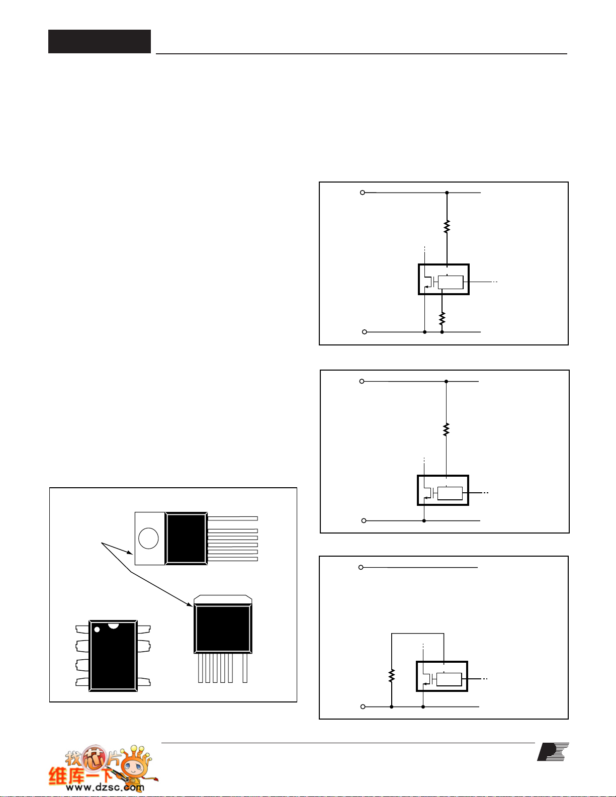
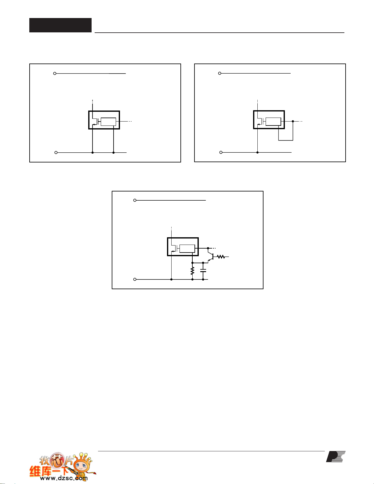
Pin Functional Description
DRAIN (D) Pin:
High voltage power MOSFET drain output. The internal
start-up bias current is drawn from this pin through a switched
high-voltage current source. Internal current limit sense point
for drain current.
CONTROL (C) Pin:
Error amplifier and feedback current input pin for duty cycle
control. Internal shunt regulator connection to provide internal
bias current during normal operation. It is also used as the
connection point for the supply bypass and auto-restart/
compensation capacitor.
LINE-SENSE (L) Pin: (Y, R or F package only)
Input pin for OV, UV, line feed forward with DC
remote ON/OFF and synchronization. A connection to SOURCE
pin disables all functions on this pin.
EXTERNAL CURRENT LIMIT (X) Pin: (Y, R or F package
only)
Input pin for external current limit adjustment, remote
ON/OFF, and synchronization. A connection to SOURCE pin
disables all functions on this pin.
reduction,
MAX
FREQUENCY (F) Pin: (Y, R or F package only)
Input pin for selecting switching frequency: 132 kHz if
connected to SOURCE pin and 66 kHz if connected to
CONTROL pin. The switching frequency is internally set for
fixed 132 kHz operation in P and G packages.
SOURCE (S) Pin:
Output MOSFET source connection for high voltage power
return. Primary side control circuit common and reference point.
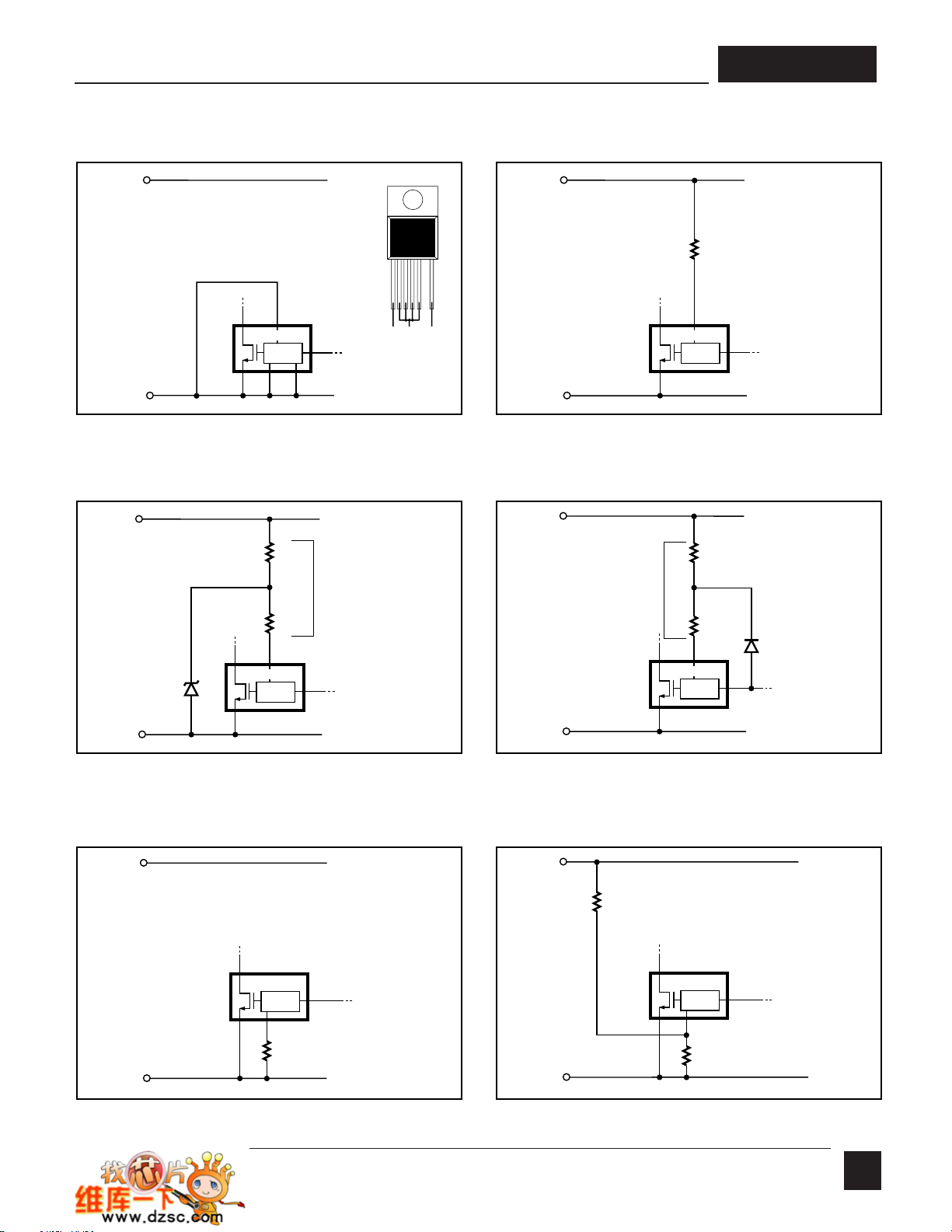
Figure 4. Y/R/F Pkg Line Sense and Externally Set Current Limit.
MULTI-FUNCTION (M) Pin:
This pin combines the functions of the LINE-SENSE (L) and
EXTERNAL CURRENT LIMIT (X) pins of the Y package
into one pin. Input pin for OV, UV, line feed forward with
DC
reduction, external current limit adjustment, remote
MAX
ON/OFF and synchronization. A connection to SOURCE pin
disables all functions on this pin and makes TOPSwitch-GX
operate in simple three terminal mode (like TOPSwitch-II).
Figure 3. Pin Configuration (top view).
4
O
11/05
(P or G package only)
Figure 5. P/G Package Line Sense.
Figure 6. P/G Package Externally Set Current Limit.
TOPSwitch-GX Family Functional
PI-2633-011502
Duty Cycle (%)
IC (mA)
TOP242-5 1.6 2.0
TOP246-9 2.2 2.6
TOP250 2.4 2.7
5.2 6.0
5.8 6.6
6.5 7.3
I
CD1
I
B
Auto-restart
IL = 125 µA
IL < I
L(DC)
IL = 190 µA
78
10
38
Frequency (kHz)
IC (mA)
30
I
CD1
I
B
Auto-restart
132
Note: For P and G packages IL is replaced with IM.
IL < I
L(DC)
IL = 125 µA
Slope = PWM Gain
IL = 190 µA
Description
Like TOPSwitch, TOPSwitch-GX is an integrated switched
mode power supply chip that converts a current at the control
input to a duty cycle at the open drain output of a high voltage
power MOSFET. During normal operation the duty cycle
of the power MOSFET decreases linearly with increasing
CONTROL pin current as shown in Figure 7.
In addition to the three terminal TOPSwitch features, such as
the high voltage start-up, the cycle-by-cycle current limiting,
loop compensation circuitry, auto-restart, thermal shutdown,
the TOPSwitch-GX incorporates many additional functions that
reduce system cost, increase power supply performance and
design flexibility. A patented high voltage CMOS technology
allows both the high voltage power MOSFET and all the low
voltage control circuitry to be cost effectively integrated onto
a single monolithic chip.
Th ree ter min als , FR EQU ENC Y, LIN E-S ENS E, a nd
EXTERNAL CURRENT LIMIT (available in Y, R or F
package) or one terminal MULTI-FUNCTION (available in P
or G package) have been added to implement some of the new
functions. These terminals can be connected to the SOURCE
pin to operate the TOPSwitch-GX in a TOPSwitch-like three
terminal mode. However, even in this three terminal mode, the
TOPSwitch-GX offers many new transparent features that do
not require any external components:
TOP242-250
1. A fully integrated 10 ms soft-start limits peak currents
and voltages during start-up and dramatically reduces or
eliminates output overshoot in most applications.
2. DC
input voltage requirement and/or higher power capability.
3. Frequency reduction at light loads lowers the switching
losses and maintains good cross regulation in multiple output
supplies.
4. Higher switching frequency of 132 kHz reduces the
transformer size with no noticeable impact on EMI.
5. Frequency jittering reduces EMI.
6. Hysteretic over-temperature shutdown ensures automatic
recovery from thermal fault. Large hysteresis prevents
circuit board overheating.
7. Packages with omitted pins and lead forming provide large
drain creepage distance.
8. Tighter absolute tolerances and smaller temperature
variations on switching frequency, current limit and PWM gain.
The LINE-SENSE (L) pin is usually used for line sensing by
connecting a resistor from this pin to the rectified DC high
voltage bus to implement line overvoltage (OV), under-voltage
(UV) and line feed-forward with DC
mode, the value of the resistor determines the OV/UV thresholds
and the DC
above the under-voltage threshold. See Table 2 and Figure 11.
of 78% allows smaller input storage capacitor, lower
MAX
is reduced linearly starting from a line voltage
MAX
reduction. In this
MAX
Figure 7. Relationship of Duty Cycle and Frequency to CONTROL
Pin Current.
The pin can also be used as a remote ON/OFF and a
synchronization input.
The EXTERNAL CURRENT LIMIT (X) pin is usually used
to reduce the current limit externally to a value close to the
operating peak current, by connecting the pin to SOURCE
through a resistor. This pin can also be used as a remote
ON/OFF and a synchronization input in both modes. See
Table 2 and Figure 11.
For the P or G packages the LINE-SENSE and EXTERNAL
CURRENT LIMIT pin functions are combined on one MULTIFUNCTION (M) pin. However, some of the functions become
mutually exclusive as shown in Table 3.
The FREQUENCY (F) pin in the Y, R or F package sets the
switching frequency to the default value of 132 kHz when
connected to SOURCE pin. A half frequency option of
66 kHz can be chosen by connecting this pin to CONTROL pin
instead. Leaving this pin open is not recommended.
11/05
O
5
TOP242-250
PI-2545-082299
S1 S2 S6 S7 S1 S2 S6 S7S0
S1 S7
S0
S0
5.8 V
4.8
V
S7
0 V
0 V
0 V
V
LINE
V
C
V
DRAIN
V
OUT
Note: S0 through S7 are the output states of the auto-restart counter
2
1
2
3
4
0 V
~
~
~
~
~
~
~
~
~
~
S6 S7
~
~
~
~
~
~
~
~
V
UV
~
~
~
~
~
~
~
~
S2
~
~
CONTROL (C) Pin Operation
The CONTROL pin is a low impedance node that is capable
of receiving a combined supply and feedback current. During
normal operation, a shunt regulator is used to separate the
feedback signal from the supply current. CONTROL pin voltage
VC is the supply voltage for the control circuitry including the
MOSFET gate driver. An external bypass capacitor closely
connected between the CONTROL and SOURCE pins is required
to supply the instantaneous gate drive current. The total amount
of capacitance connected to this pin also sets the auto-restart
timing as well as control loop compensation.
When rectified DC high voltage is applied to the DRAIN
pin during start-up, the MOSFET is initially off, and the
CONTROL pin capacitor is charged through a switched high
voltage current source connected internally between the DRAIN
and CONTROL pins. When the CONTROL pin voltage VC
reaches approximately 5.8 V, the control circuitry is activated
and the soft-start begins. The soft-start circuit gradually
increases the duty cycle of the MOSFET from zero to the
maximum value over approximately 10 ms. If no external
feedback/supply current is fed into the CONTROL pin by the
end of the soft-start, the high voltage current source is turned
off and the CONTROL pin will start discharging in response
to the supply current drawn by the control circuitry. If the
power supply is designed properly, and no fault condition
such as open loop or shorted output exists, the feedback loop
will close, providing external CONTROL pin current, before
the CONTROL pin voltage has had a chance to discharge to
the lower threshold voltage of approximately 4.8 V (internal
supply under-voltage lockout threshold). When the externally
fed current charges the CONTROL pin to the shunt regulator
voltage of 5.8 V, current in excess of the consumption of the
chip is shunted to SOURCE through resistor R
E
Figure 2. This current flowing through RE controls the duty cycle
of the power MOSFET to provide closed loop regulation. The
shunt regulator has a finite low output impedance ZC that sets
the gain of the error amplifier when used in a primary feedback
configuration. The dynamic impedance ZC of the CONTROL
pin together with the external CONTROL pin capacitance sets
the dominant pole for the control loop.
When a fault condition such as an open loop or shorted output
prevents the flow of an external current into the CONTROL
pin, the capacitor on the CONTROL pin discharges towards
4.8 V. At 4.8 V, auto-restart is activated which turns the output
MOSFET off and puts the control circuitry in a low current
standby mode. The high-voltage current source turns on and
charges the external capacitance again. A hysteretic internal
supply under-voltage comparator keeps V
within a window
C
of typically 4.8 V to 5.8 V by turning the high-voltage current
source on and off as shown in Figure 8. The auto-restart
circuit has a divide-by-eight counter which prevents the output
MOSFET from turning on again until eight discharge/charge
cycles have elapsed. This is accomplished by enabling the
output MOSFET only when the divide-by-eight counter reaches
full count (S7). The counter effectively limits TOPSwitch-GX
power dissipation by reducing the auto-restart duty cycle
to typically 4%. Auto-restart mode continues until output
voltage regulation is again achieved through closure of the
feedback loop.
Oscillator and Switching Frequency
The internal oscillator linearly charges and discharges an
as shown in
Figure 8. Typical Waveforms for (1) Power Up (2) Normal Operation (3) Auto-Restart (4) Power Down.
O
11/05
6
internal capacitance between two voltage levels to create
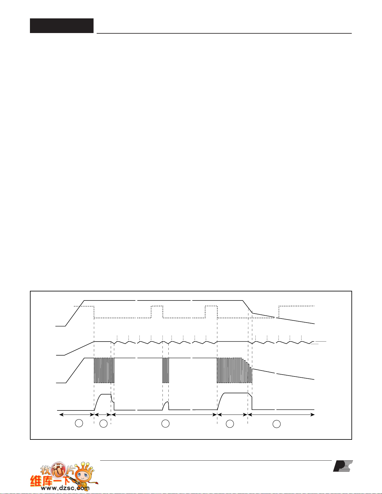
PI-2550-092499
128 kHz
4 ms
Time
Switching
Frequency
V
DRAIN
136 kHz
a sawtooth waveform for the pulse width modulator. This
oscillator sets the pulse width modulator/current limit latch at
the beginning of each cycle.
The nominal switching frequency of 132 kHz was chosen to
minimize transformer size while keeping the fundamental EMI
frequency below 150 kHz. The FREQUENCY pin (available
only in Y, R or F package), when shorted to the CONTROL pin,
lowers the switching frequency to 66 kHz (half frequency) which
may be preferable in some cases such as noise sensitive video
applications or a high efficiency standby mode. Otherwise, the
FREQUENCY pin should be connected to the SOURCE pin
for the default 132 kHz.
TOP242-250
Figure 9. Switching Frequency Jitter (Idealized V
Waveforms).
DRAIN
To further reduce the EMI level, the switching frequency is
jittered (frequency modulated) by approximately ±4 kHz at
250 Hz (typical) rate as shown in Figure 9. Figure 46 shows
the typical improvement of EMI measurements with frequency
jitter.
Pulse Width Modulator and Maximum Duty Cycle
The pulse width modulator implements voltage mode control
by driving the output MOSFET with a duty cycle inversely
proportional to the current into the CONTROL pin
that
is in excess of the internal supply current of the chip (see
Figure 7). The excess current is the feedback error signal that
appears across RE (see Figure 2). This signal is filtered by an RC
network with a typical corner frequency of 7 kHz to reduce the
effect of switching noise in the chip supply current generated
by the MOSFET gate driver. The filtered error signal is
compared with the internal oscillator sawtooth waveform to
generate the duty cycle waveform. As the control current
increases, the duty cycle decreases. A clock signal from the
oscillator sets a latch which turns on the output MOSFET. The
pulse width modulator resets the latch, turning off the output
MOSFET. Note that a minimum current must be driven into
the CONTROL pin before the duty cycle begins to change.
The maximum duty cycle, DC
is set at a default maximum
MAX,
value of 78% (typical). However, by connecting the LINESENSE or MULTI-FUNCTION pin (depending on the
package) to the rectified DC high voltage bus through a
resistor with appropriate value, the maximum duty cycle can
be made to decrease from 78% to 38% (typical) as shown in
Figure 11 when input line voltage increases (see line feed
forward with DC
reduction).
MAX
Light Load Frequency Reduction
The pulse width modulator duty cycle reduces as the load at
the power supply output decreases. This reduction in duty
cycle is proportional to the current flowing into the CONTROL
pin. As the CONTROL pin current increases, the duty cycle
decreases linearly towards a duty cycle of 10%. Below 10%
duty cycle, to maintain high efficiency at light loads, the
frequency is also reduced linearly until a minimum frequency
is reached at a duty cycle of 0% (refer to Figure 7). The
minimum frequency is typically 30 kHz and 15 kHz for
132 kHz and 66 kHz operation, respectively.
This feature allows a power supply to operate at lower
frequency at light loads thus lowering the switching losses
while maintaining good cross regulation performance and low
output ripple.
Error Amplifier
The shunt regulator can also perform the function of an error
amplifier in primary side feedback applications. The shunt
regulator voltage is accurately derived from a temperaturecompensated bandgap reference. The gain of the error
amplifier is set by the CONTROL pin dynamic impedance.
The CONTROL pin clamps external circuit signals to the V
voltage level. The CONTROL pin current in excess of the
supply current is separated by the shunt regulator and flows
through RE as a voltage error signal.
On-Chip Current Limit with External Programmability
The cycle-by-cycle peak drain current limit circuit uses the
output MOSFET ON-resistance as a sense resistor. A current
limit comparator compares the output MOSFET on-state drain
to source voltage, V
current causes V
DS(ON)
with a threshold voltage. High drain
DS(ON)
to exceed the threshold voltage and turns
the output MOSFET off until the start of the next clock cycle.
The current limit comparator threshold voltage is temperature
compensated to minimize the variation of the current limit due
to temperature related changes in R
of the output MOSFET.
DS(ON)
The default current limit of TOPSwitch-GX is preset internally.
However, with a resistor connected between EXTERNAL
CURRENT LIMIT (X) pin (Y, R or F package) or MULTIFUNCTION (M) pin (P or G package) and SOURCE pin,
current limit can be programmed externally to a lower level
between 30% and 100% of the default current limit. Please
refer to the graphs in the typical performance characteristics
section for the selection of the resistor value. By setting current
limit low, a larger TOPSwitch-GX than necessary for the power
C
11/05
O
7
TOP242-250
PI-2637-060600
Oscillator
(SAW)
D
MAX
Enable from
X, L or M Pin (STOP)
Time
required can be used to take advantage of the lower R
DS(ON)
for
higher efficiency/smaller heat sinking requirements. With
a second resistor connected between the EXTERNAL
CURRENT LIMIT (X) pin (Y, R or F package) or MULTIFUNCTION (M) pin (P or G package) and the rectified DC
high voltage bus, the current limit is reduced with increasing
line voltage, allowing a true power limiting operation against
line variation to be implemented. When using an RCD clamp,
this power limiting technique reduces maximum clamp
voltage at high line. This allows for higher reflected voltage
designs as well as reducing clamp dissipation.
The leading edge blanking circuit inhibits the current limit
comparator for a short time after the output MOSFET is turned
on. The leading edge blanking time has been set so that, if a
power supply is designed properly, current spikes caused by
primary-side capacitances and secondary-side rectifier reverse
recovery time should not cause premature termination of the
switching pulse.
The current limit is lower for a short period after the leading
edge blanking time as shown in Figure 52. This is due to
dynamic characteristics of the MOSFET. To avoid triggering
the current limit in normal operation, the drain current waveform
should stay within the envelope shown.
Line Under-Voltage Detection (UV)
At power up, UV keeps TOPSwitch-GX off until the input line
voltage reaches the under-voltage threshold. At power down,
UV prevents auto-restart attempts after the output goes out
of regulation. This eliminates power down glitches caused
by slow discharge of the large input storage capacitor present
in applications such as standby supplies. A single resistor
connected from the LINE-SENSE pin (Y, R or F package) or
MULTI-FUNCTION pin (P or G package) to the rectified DC
high voltage bus sets UV threshold during power up. Once the
power supply is successfully turned on, the UV threshold is
lowered to 40% of the initial UV threshold to allow extended
input voltage operating range (UV low threshold). If the UV
low threshold is reached during operation without the power
supply losing regulation, the device will turn off and stay off
until UV (high threshold) has been reached again. If the power
supply loses regulation before reaching the UV low threshold,
the device will enter auto-restart. At the end of each autorestart cycle (S7), the UV comparator is enabled. If the UV
high threshold is not exceeded the MOSFET will be disabled
during the next cycle (see Figure 8). The UV feature can
be disabled independent of the OV feature as shown in
Figures 19 and 23.
Line Overvoltage Shutdown (OV)
The same resistor used for UV also sets an overvoltage threshold
which, once exceeded, will force TOPSwitch-GX output into
off-state. The ratio of OV and UV thresholds is preset at 4.5
as can be seen in Figure 11. When the MOSFET is off, the
rectified DC high voltage surge capability is increased to the
voltage rating of the MOSFET (700 V), due to the absence
of the reflected voltage and leakage spikes on the drain. A
small amount of hysteresis is provided on the OV threshold to
prevent noise triggering. The OV feature can be disabled
independent of the UV feature as shown in Figures 18 and 32.
Line Feed-Forward with DC
Reduction
MAX
The same resistor used for UV and OV also implements line
voltage feed-forward, which minimizes output line ripple and
reduces power supply output sensitivity to line transients.
This feed-forward operation is illustrated in Figure 7 by the
different values of IL (Y, R or F package) or IM (P or G package).
Note that for the same CONTROL pin current, higher line
voltage results in smaller operating duty cycle. As an added
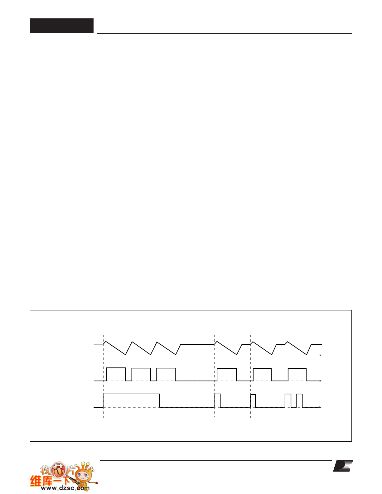
Figure 10. Synchronization Timing Diagram.
O
11/05
8

TOP242-250
feature, the maximum duty cycle DC
is also reduced
MAX
from 78% (typical) at a voltage slightly higher than the UV
threshold to 30% (typical) at the OV threshold (see Figure 11).
Limiting DC
at higher line voltages helps prevent transformer
MAX
saturation due to large load transients in TOP248, TOP249 and
TOP250 forward converter applications. DC
of 38% at
MAX
high line was chosen to ensure that the power capability of the
TOPSwitch-GX is not restricted by this feature under normal
operation.
Remote ON/OFF and Synchronization
TOPSwitch-GX can be turned on or off by controlling the
current into the LINE-SENSE pin or out from the EXTERNAL
CURRENT LIMIT pin (Y, R or F package) and into or out
from the MULTI-FUNCTION pin (P or G package) (see
Figure 11). In addition, the LINE-SENSE pin has a 1 V
threshold comparator connected at its input. This voltage
threshold can also be used to perform remote ON/OFF
control. This al lo ws easy implementation of remote
ON/OFF control of TOPSwitch-GX in several different ways.
A transistor or an optocoupler output connected between
the EXTERNAL CURRENT LIMIT or LINE-SENSE pins
(Y, R or F package) or the MULTI-FUNCTION pin (P or G
package) and the SOURCE pin implements this function with
“active-on” (Figures 22, 29 and 36) while a transistor or an
optocoupler output connected between the LINE-SENSE pin
(Y, R or F package) or the MULTI-FUNCTION (P or G package)
pin and the CONTROL pin implements the function with
“active-off” (Figures 23 and 37).
When a signal is received at the LINE-SENSE pin or the
EXTERNAL CURRENT LIMIT pin (Y, R or F package) or
the MULTI-FUNCTION pin (P or G package) to disable the
output through any of the pin functions such as OV, UV and
remote ON/OFF, TOPSwitch-GX always completes its current
switching cycle, as illustrated in Figure 10, before the output is
forced off. The internal oscillator is stopped slightly before the
end of the current cycle and stays there as long as the disable
signal exists. When the signal at the above pins changes state
from disable to enable, the internal oscillator starts the next
switching cycle. This approach allows the use of these pins
to synchronize TOPSwitch-GX to any external signal with a
frequency between its internal switching frequency and 20 kHz.
cycles between 4.8 V and 5.8 V (see CONTROL pin operation
section above) and runs entirely off the high voltage DC input,
but with very low power consumption (160 mW typical at
230 VAC with M or X pins open). When the TOPSwitch-GX
is remotely turned on after entering this mode, it will initiate
a normal start-up sequence with soft-start the next time the
CONTROL pin reaches 5.8 V. In the worst case, the delay from
remote on to start-up can be equal to the full discharge/charge
cycle time of the CONTROL pin, which is approximately
125 ms for a 47
µF CONTROL pin capacitor. This
reduced consumption remote off mode can eliminate
expensive and unreliable in-line mechanical switches. It also
allows for microprocessor controlled turn-on and turn-off
sequences that may be required in certain applications such as
inkjet and laser printers.
Soft-Start
Two on-chip soft-start functions are activated at start-up with a
duration of 10 ms (typical). Maximum duty cycle starts from
0% and linearly increases to the default maximum of 78% at
the end of the 10 ms duration and the current limit starts from
about 85% and linearly increases to 100% at the end of the
10 ms duration. In addition to start-up, soft-start is also
activated at each restart attempt during auto-restart and when
restarting after being in hysteretic regulation of CONTROL
pin voltage (V
), due to remote OFF or thermal shutdown
C
conditions. This effectively minimizes current and voltage
stresses on the output MOSFET, the clamp circuit and the
output rectifier during start-up. This feature also helps
minimize output overshoot and prevents saturation of the
transformer during start-up.
Shutdown/Auto-Restart
To minimize TOPSwitch-GX power dissipation under fault
conditions, the shutdown/auto-restart circuit turns the power
supply on and off at an auto-restart duty cycle of typically 4%
if an out of regulation condition persists. Loss of regulation
interrupts the external current into the CONTROL pin. V
regulation changes from shunt mode to the hysteretic autorestart mode as described in CONTROL pin operation section.
When the fault condition is removed, the power supply output
becomes regulated, V
regulation returns to shunt mode, and
C
normal operation of the power supply resumes.
C
As seen above, the remote ON/OFF feature allows the
TOPSwitch-GX to be turned on and off instantly, on a cycleby-cycle basis, with very little delay. However, remote
ON/OFF can also be used as a standby or power switch to
turn off the TOPSwitch-GX and keep it in a very low power
consumption state for indefinitely long periods. If the
TOPSwitch-GX is held in remote off state for long enough
time to allow the CONTROL pin to discharge to the internal
supply under-voltage threshold of 4.8 V (approximately 32 ms
for a 47
µF CONTROL pin capacitance), the CONTROL pin
goes into the hysteretic mode of regulation. In this mode, the
CONTROL pin goes through alternate charge and discharge
Hysteretic Over-Temperature Protection
Temperature protection is provided by a precision analog
circuit that turns the output MOSFET off when the junction
temperature exceeds the thermal shutdown temperature
(140 °C typical). When the junction temperature cools to
below the hysteretic temperature, normal operation resumes
providing automatic recovery. A large hysteresis of 70
(typical) is provided to prevent overheating of the PC board due
to a continuous fault condition. V
is regulated in hysteretic mode
C
and a 4.8 V to 5.8 V (typical) sawtooth waveform is present on
the CONTROL pin while in thermal shutdown.
11/05
°C
O
9
TOP242-250
Bandgap Reference
All critical TOPSwitch-GX internal voltages are derived from
a temperature-compensated bandgap reference. This reference
is also used to generate a temperature-compensated current
reference, which is trimmed to accurately set the switching
frequency, MOSFET gate drive current, current limit, and the
line OV/UV thresholds. TOPSwitch-GX has improved circuitry
to maintain all of the above critical parameters within very tight
absolute and temperature tolerances.
High-Voltage Bias Current Source
This current source biases TOPSwitch-GX from the DRAIN
pin and charges the CONTROL pin external capacitance
during start-up or hysteretic operation. Hysteretic operation
occurs during auto-restart, remote OFF and over-temperature
shutdown. In this mode of operation, the current source
is switched on and off with an effective duty cycle of
approximately 35%. This duty cycle is determined by the
ratio of CONTROL pin charge (IC) and discharge currents
(I
CD1
and I
). This current source is turned off during normal
CD2
operation when the output MOSFET is switching. The effect of
the current source switching will be seen on the DRAIN voltage
waveform as small disturbances and is normal.
Using Feature Pins
FREQUENCY (F) Pin Operation
The FREQUENCY pin is a digital input pin available in the
Y, R or F package only. Shorting the FREQUENCY pin to
SOURCE pin selects the nominal switching frequency of
132 kHz (Figure 13), which is suited for most applications.
For other cases that may benefit from lower switching
frequency such as noise sensitive video applications, a
66 kHz switching frequency (half frequency) can be selected by
shorting the FREQUENCY pin to the CONTROL pin
(Figure 14). In addition, an example circuit shown in Figure 15
may be used to lower the switching frequency from 132 kHz in
normal operation to 66 kHz in standby mode for very low
standby power consumption.
LINE-SENSE (L) Pin Operation (Y, R and F Packages)
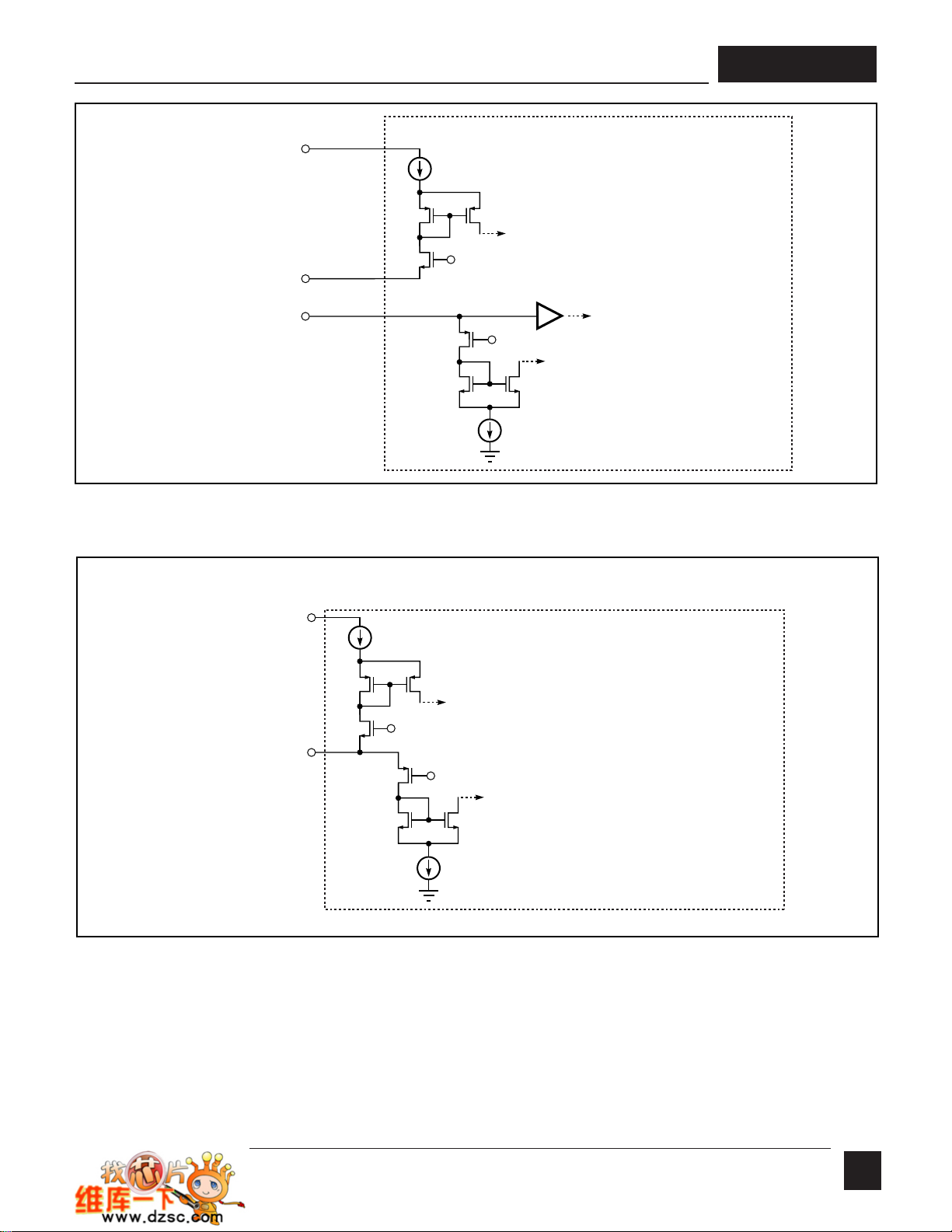
When current is fed into the LINE-SENSE pin, it works as
a voltage source of approximately 2.6 V up to a maximum
current of +400 µA (typical). At +400 µA, this pin turns into
a constant current sink. Refer to Figure 12a. In addition, a
comparator with a threshold of 1 V is connected at the pin and
is used to detect when the pin is shorted to the SOURCE pin.
There are a total of four functions available through the use of
the LINE-SENSE pin: OV, UV, line feed-forward with DC
reduction, and remote ON/OFF. Connecting the LINE-SENSE
pin to the SOURCE pin disables all four functions. The LINESENSE pin is typically used for line sensing by connecting a
resistor from this pin to the rectified DC high voltage bus to
implement OV, UV and DC
reduction with line voltage. In
MAX
this mode, the value of the resistor determines the line OV/UV
thresholds, and the DC
is reduced linearly with rectified DC
MAX
high voltage starting from just above the UV threshold. The pin
can also be used as a remote ON/OFF and a synchronization
input. Refer to Table 2 for possible combinations of the functions
with example circuits shown in Figure 16 through Figure 40. A
description of specific functions in terms of the LINE-SENSE
pin I/V characteristic is shown in Figure 11 (right hand side).
The horizontal axis represents LINE-SENSE pin current with
positive polarity indicating currents flowing into the pin. The
meaning of the vertical axes varies with functions. For those
that control the ON/OFF states of the output such as UV, OV
and remote ON/OFF, the vertical axis represents the enable/
disable states of the output. UV triggers at IUV (+50 µA typical
with 30 µA hysteresis) and OV triggers at IOV (+225 µA
typical with 8 µA hysteresis). Between the UV and OV
thresholds, the output is enabled. For line feed-forward with
MAX
LINE-SENSE AND EXTERNAL CURRENT LIMIT PIN TABLE*
Figure Number 16 17 18 19 20 21 22 23 24 25 26 27 28 29
Three Terminal Operation
Under-Voltage
Overvoltage
Line Feed-Forward (DC
Overload Power Limiting
External Current Limit
Remote ON/OFF
*This table is only a partial list of many LINE-SENSE and EXTERNAL CURRENT LIMIT pin configurations that are possible.
Table 2. Typical LINE-SENSE and EXTERNAL CURRENT LIMIT Pin Configurations.
O
11/05
10
▼
MAX
✓
✓ ✓ ✓ ✓ ✓
✓ ✓ ✓ ✓ ✓
)
✓ ✓ ✓ ✓
✓
✓ ✓ ✓ ✓ ✓ ✓
✓ ✓ ✓ ✓ ✓ ✓ ✓
TOP242-250
DC
reduction, the vertical axis represents the magnitude of
MAX
the DC
maximum duty cycle from 78% at I
. Line feed-forward with DC
MAX
reduction lowers
MAX
(+60 µA typical) to
L(DC)
38% at IOV (+225 µA).
EXTERNAL CURRENT LIMIT (X) Pin Operation
(Y, R and F Packages)
When current is drawn out of the EXTERNAL CURRENT
LIMIT pin, it works as a voltage source of approximately
1.3 V up to a maximum current of -240 µA (typical). At
-240 µA, it turns into a constant current source (refer to
Figure 12a).
There are two functions available through the use of the
EXTERNAL CURRENT LIMIT pin: external current limit
and remote ON/OFF. Connecting the EXTERNAL CURRENT
LIMIT pin to the SOURCE pin disables the two functions. In
high efficiency applications, this pin can be used to reduce the
current limit externally to a value close to the operating peak
current by connecting the pin to the SOURCE pin through
a resistor. The pin can also be used for remote ON/OFF.
Table 2 shows several possible combinations using this pin. See
Figure 11 for a description of the functions where the horizontal
axis (left hand side) represents the EXTERNAL CURRENT
LIMIT pin current. The meaning of the vertical axes varies
with function. For those that control the ON/OFF states of the
output such as remote ON/OFF, the vertical axis represents the
enable/disable states of the output. For external current limit,
the vertical axis represents the magnitude of the I
LIMIT
. Please
see graphs in the Typical Performance Characteristics section
for the current limit programming range and the selection of
appropriate resistor value.
MULTI-FUNCTION (M) Pin Operation (P and G
Packages)
The LINE-SENSE and EXTERNAL CURRENT LIMIT pin
functions are combined to a single MULTI-FUNCTION pin
for P and G packages. The comparator with a 1 V threshold
at the LINE-SENSE pin is removed in this case as shown in
Figure 2b. All of the other functions are kept intact. However,
since some of the functions require opposite polarity of input
current (MULTI-FUNCTION pin), they are mutually exclusive.
For example, line sensing features cannot be used simultaneously
with external current limit setting. When current is fed into
the MULTI-FUNCTION pin, it works as a voltage source of
approximately 2.6 V up to a maximum current of +400 µA
(typical). At +400 µA, this pin turns into a constant current
sink. When current is drawn out of the MULTI-FUNCTION
pin, it works as a voltage source of approximately 1.3 V up to
a maximum current of -240 µA (typical). At -240 µA, it turns
into a constant current source. Refer to Figure 12b.
There are a total of five functions available through the use
of the MULTI-FUNCTION pin: OV, UV, line feed-forward
with DC
reduction, external current limit and remote
MAX
ON/OFF. A short circuit between the MULTI-FUNCTION
pin and SOURCE pin disables all five functions and forces
TOPSwitch-GX to operate in a simple three terminal mode
like TOPSwitch-II. The MULTI-FUNCTION pin is typically
used for line sensing by connecting a resistor from this pin to
the rectified DC high voltage bus to implement OV, UV and
DC
reduction with line voltage. In this mode, the value
MAX
of the resistor determines the line OV/UV thresholds, and the
DC
is reduced linearly with increasing rectified DC high
MAX
voltage starting from just above the UV threshold. External
current limit programming is implemented by connecting the
MULTI-FUNCTION pin to the SOURCE pin through a resistor.
However, this function is not necessary in most applications
since the internal current limit of the P and G package devices
has been reduced, compared to the Y, R and F package
devices, to match the thermal dissipation capability of the P
and G packages. It is therefore recommended that the MULTIFUNCTION pin is used for line sensing as described above and
not for external current limit reduction. The same pin can also
MULTI-FUNCTION PIN TABLE*
Figure Number 30 31 32 33 34 35 36 37 38 39 40
Three Terminal Operation
Under-Voltage
Overvoltage
Line Feed-Forward (DC
Overload Power Limiting
External Current Limit
Remote ON/OFF
*This table is only a partial list of many MULTI-FUNCTION pin configurations that are possible.
Table 3. Typcial MULTI-FUNCTION Pin Configurations.
▼
MAX
✓
✓ ✓ ✓
✓ ✓ ✓
)
✓ ✓
✓
✓ ✓ ✓ ✓
✓ ✓ ✓ ✓ ✓
O
11/05
11

TOP242-250
-250 -200 -150 -100 -50 0 50 100 150 200 250 300 350 400
PI-2636-010802
Output
MOSFET
Switching
(Enabled)
(Disabled)
I
LIMIT
(Default)
DC
MAX
(78.5%)
Current
Limit
M Pin
L PinX Pin
Maximum
Duty Cycle
V
BG
-22 µA
-27 µA
V
BG
+ V
TP
I
I
I
I
I
UV
I
REM(N)
I
OV
Pin Voltage
Note: This figure provides idealized functional characteristics with typical performance values. Please refer to the parametric
table and typical performance characteristics sections of the data sheet for measured data.
X and L Pins (Y, R or F Package) and M Pin (P or G Package) Current (µA)
Disabled when supply
output goes out of
regulation
Figure 11. MULTI-FUNCTION (P or G package), LINSE-SENSE, and EXTERNAL CURRENT LIMIT (Y, R or F package) Pin Characteristics.
be used as a remote ON/OFF and a synchronization input in
both modes. Please refer to Table 3 for possible combinations
of the functions with example circuits shown in Figure 30
through Figure 40. A description of specific functions in terms
of the MULTI-FUNCTION pin I/V characteristic is shown in
Figure 11. The horizontal axis represents MULTI-FUNCTION
pin current with positive polarity indicating currents flowing into
the pin. The meaning of the vertical axes varies with functions.
For those that control the ON/OFF states of the output such
as UV, OV and remote ON/OFF, the vertical axis represents
the enable/disable states of the output. UV triggers at IUV
(+50 µA typical) and OV triggers at IOV (+225 µA typical with
30 µA hysteresis). Between the UV and OV thresholds, the
output is enabled. For external current limit and line feedforward with DC
magnitude of the I
DC
reduction lowers maximum duty cycle from 78% at I
MAX
(+60 µA typical) to 38% at IOV (+225 µA). External current
reduction, the vertical axis represents the
MAX
LIMIT
and DC
MAX
. Line feed-forward with
M(DC)
limit is available only with negative MULTI-FUNCTION
pin current. Please see graphs in the Typical Performance
Characteristics section for the current limit programming
range and the selection of appropriate resistor value.
O
11/05
12
VBG + V
T
1 V
V
BG
240 µA
400 µA
CONTROL (C)
Y, R and F Package
(Voltage Sense)
(Positive Current Sense - Under-Voltage,
Overvoltage, ON/OFF Maximum Duty
Cycle Reduction)
(Negative Current Sense - ON/OFF,
Current Limit Adjustment)
PI-2634-022604
TOPSwitch-GX
LINE-SENSE (L)
EXTERNAL CURRENT LIMIT (X)
VBG + V
T
V
BG
240 µA
400 µA
CONTROL (C)
MULTI-FUNCTION (M)
(Positive Current Sense - Under-Voltage,
Overvoltage, Maximum Duty
Cycle Reduction)
(Negative Current Sense - ON/OFF,
Current Limit Adjustment)
PI-2548-022604
TOPSwitch-GX
P and G Package
Figure 12a. LINE-SENSE (L), and EXTERNAL CURRENT LIMIT (X) Pin Input Simplified Schematic.
TOP242-250
Figure 12b. MULTI-FUNCTION (M) Pin Input Simplified Schematic.
11/05
O
13
TOP242-250
PI-2654-071700
DC
Input
Voltage
+
-
D
S
C
CONTROL
F
PI-2655-071700
DC
Input
Voltage
+
-
D
S
C
CONTROL
F
PI-2656-040501
DC
Input
Voltage
+
-
D
S
C
STANDBY
QS can be an optocoupler output.
CONTROL
F
20
kΩ
R
HF
1 nF
Q
S
47 kΩ
Typical Uses of FREQUENCY (F) PIN
Figure 13. Full Frequency Operation (132 kHz). Figure 14. Half Frequency Operation (66 kHz).
14
O
11/05
Figure 15. Half Frequency Standby Mode (For High Standby
Efficiency).
TOP242-250
X F
PI-2617-050100
DC
Input
Voltage
+
-
D
C S
D
S
C
CONTROL
L
C L X S F D
PI-2618-081403
DC
Input
Voltage
+
-
D
S
C
CONTROL
L
2 MΩR
LS
VUV = IUV x R
LS
V
OV = IOV x RLS
For RLS = 2 MΩ
V
UV
= 100 VDC
V
OV =
450 VDC
DC
MAX
@100 VDC = 78%
DC
MAX
@375 VDC = 38%
PI-2510-040501
DC
Input
Voltage
+
-
D M
S
C
VUV = RLS x I
UV
For Value Shown
VUV = 100 VDC
R
LS
6.2 V
2
MΩ
22
kΩ
CONTROL
PI-2620-040501
DC
Input
Voltage
+
-
D
S
C
CONTROL
L
2 MΩ
30 kΩ
R
LS
1N4148
V
OV
= I
OV x RLS
For Values Shown
VOV = 450 VDC
X
PI-2623-092303
DC
Input
Voltage
+
-
D
S
C
R
IL
For R
IL
= 12 kΩ
I
LIMIT
= 69%
See Figure 54b for
other resistor values
(R
IL
)
For
R
IL
= 25 kΩ
I
LIMIT
= 43%
CONTROL
X
PI-2624-040501
DC
Input
Voltage
+
-
D
S
C
2.5 MΩ
R
LS
6 kΩ
R
IL
100% @ 100 VDC
63% @ 300 VDC
I
LIMIT
=
I
LIMIT
=
CONTROL
Typical Uses of LINE-SENSE (L) and EXTERNAL CURRENT LIMIT (X) P ins
Figure 16. Three Terminal Operation (LINE-SENSE and
EXTERNAL CURRENT LIMIT Features Disabled.
FREQUENCY Pin Tied to SOURCE or CONTROL Pin).
Figure 18. Line-Sensing for Under-Voltage Only (Overvoltage
Disabled).
Figure 17. Line-Sensing for Under-Voltage, Overvoltage and Line
Feed-Forward.
Figure 19. Linse-Sensing for Overvoltage Only (Under-Voltage
Disabled). Maximum Duty Cycle Reduced at Low Line
and Further Reduction with Increasing Line Voltage.
Figure 20. Externally Set Current Limit.
Figure 21. Current Limit Reduction with Line Voltage.
O
11/05
15
TOP242-250
X
PI-2625-040501
DC
Input
Voltage
+
-
D
S
C
ON/OFF
47 KΩ
QR can be an optocoupler
output or can be replaced by
a manual switch.
Q
R
CONTROL
PI-2621-040501
DC
Input
Voltage
+
-
D
S
C
CONTROL
L
47 kΩ
Q
R
R
MC
45 kΩ
QR can be an
optocoupler output or
can be replaced
by a manual switch.
ON/OFF
X
ON/OFF
47 kΩ
PI-2626-040501
DC
Input
Voltage
+
-
D
S
C
R
IL
Q
R
12 kΩ
For
R
IL
=
I
LIMIT
= 69%
25
kΩ
For
R
IL
=
I
LIMIT
= 43%
QR can be an optocoupler
output or can be replaced
by a manual switch.
CONTROL
PI-2627-040501
DC
Input
Voltage
+
-
D
S
C
CONTROL
L
47 kΩ
Q
R
R
MC
45 kΩ
QR can be an
optocoupler output
or can be replaced
by a manual switch.
ON/OFF
X
R
IL
PI-2622-040501
DC
Input
Voltage
+
-
D
S
C
CONTROL
L
47 kΩ
2
MΩ
Q
R
R
LS
ON/OFF
For RLS = 2 MΩ
V
UV
= 100 VDC
V
OV
= 450 VDC
QR can be an optocoupler
output or can be replaced
by a manual switch.
X
ON/OFF
47 kΩ
PI-2628-040501
DC
Input
Voltage
+
-
D
S
C
CONTROL
L
R
IL
R
LS
Q
R
2 MΩ
VUV = IUV x R
LS
V
OV = IOV x RLS
DC
MAX
@100 VDC = 78%
DC
MAX
@375 VDC = 38%
12 kΩ
For
R
IL
=
I
LIMIT
= 69%
QR can be an optocoupler
output or can be replaced
by a manual switch.
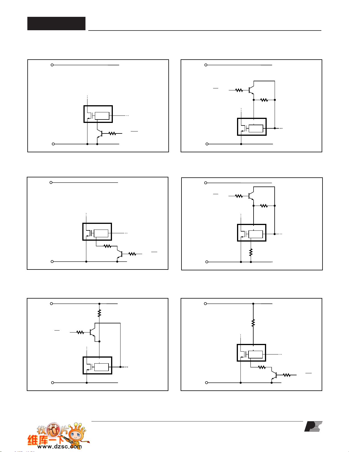
Typical Uses of LINE-SENSE (L) and EXTERNAL CURRENT LIMIT (X) Pins (cont.)
Figure 22. Active-on (Fail Safe) Remove ON/OFF. Figure 23. Active-off Remote ON/OFF. Maximum Duty Cycle
Reduced.
Figure 24. Active-on Remote ON/OFF with Externally Set Current
Limit.
Figure 26. Active-off Remote ON/OFF with LINE-SENSE. Figure 27. Active-on Remote ON/OFF with LINE-SENSE and
16
O
11/05
Figure 25. Active-off Remote ON/OFF with Externally Set Current
Limit.
EXTERNAL CURRENT LIMIT.

TOP242-250
X
PI-2629-092203
DC
Input
Voltage
+
-
D
S
C
CONTROL
L
R
IL
R
LS
12 kΩ
2
MΩ
VUV = IUV x R
LS
V
OV = IOV x RLS
For RLS = 2 MΩ
DC
MAX
@100 VDC = 78%
DC
MAX
@375 VDC = 38%
For
RIL = 12 kΩ
I
LIMIT
= 69%
See Figure 54b for
other resistor values
(R
IL
) to select different
I
LIMIT
values
VUV = 100 VDC
VOV = 450 VDC
PI-2640-040501
DC
Input
Voltage
+
-
D
S
C
CONTROL
L
ON/OFF
47 kΩ
QR can be an optocoupler
output or can be replaced by
a manual switch.
300 kΩ
Q
R
PI-2508-081199
DC
Input
Voltage
+
-
D
S
C
CONTROL
M
C
D S
C D
S
S
S S
M
PI-2509-040501
DC
Input
Voltage
+
-
D M
S
C
VUV = IUV x R
LS
V
OV = IOV x RLS
For RLS = 2 MΩ
VUV = 100 VDC
V
OV =
450 VDC
DC
MAX
@100 VDC = 78%
DC
MAX
@375 VDC = 38%
CONTROL
R
LS
2 MΩ
PI-2510-040501
DC
Input
Voltage
+
-
D M
S
C
VUV = RLS x I
UV
For Value Shown
VUV = 100 VDC
R
LS
6.2 V
2
MΩ
22
kΩ
CONTROL
PI-2516-040501
DC
Input
Voltage
+
-
D M
S
C
V
OV
= I
OV x RLS
For Values Shown
V
OV
= 450 VDC
CONTROL
R
LS
1N4148
2
MΩ
30
kΩ
Typical Uses of LINE-SENSE (L) and EXTERNAL CURRENT LIMIT (X) Pins (cont.)
Figure 28. Line-Sensing and Externally Set Current Limit. Figure 29. Active-on Remote ON/OFF.
Typical Uses of MULTI-FUNCTION (M) Pin
Figure 30. Three Terminal Operation (MULIT-FUNCTION Features
Disabled).
Figure 32. Line-Sensing for Under-Voltage Only (Overvoltage
Disabled).
Figure 31. Line-Sensing for Undervoltage, Over-Voltage and Line
Feed-Forward.
Figure 33. Line-Sensing for Overvoltage Only (Under-Voltage
Disabled). Maximum Duty Cycle Reduced at Low Line
and Further Reduction with Increasing Line Voltage.
O
11/05
17

TOP242-250
PI-2517-022604
DC
Input
Voltage
+
-
D M
S
C
For R
IL
= 12 kΩ
I
LIMIT
= 69%
CONTROL
R
IL
See Figures 54b, 55b
and 56b for other resistor
values (R
IL
) to select
different
I
LIMIT
values.
For R
IL
= 25 kΩ
I
LIMIT
= 43%
PI-2518-040501
DC
Input
Voltage
+
-
D M
S
C
CONTROL
R
IL
RLS2.5 MΩ
6
kΩ
100% @ 100 VDC
63% @ 300 VDC
I
LIMIT
=
I
LIMIT
=
PI-2519-040501
DC
Input
Voltage
+
-
D
S
C
Q
R
ON/OFF
M
CONTROL
QR can be an optocoupler
output or can be replaced
by a manual switch.
47 kΩ
PI-2522-040501
DC
Input
Voltage
+
-
D
S
C
R
MC
45 kΩ
M
CONTROL
Q
R
QR can be an optocoupler
output or can be replaced
by a manual switch.
ON/OFF
47 kΩ
Typical Uses of MULTI-FUNCTION (M) Pin (cont.)
Figure 34. Externally Set Current Limit (Not Normally Required-See
M Pin Operation Description).
Figure 36. Active-on (Fail Safe) Remote ON/OFF.
Figure 35. Current Limit Reduction with Line Voltage (Not Normally
Required-See M Pin Operation Description).
Figure 37. Active-off Remote ON/OFF. Maximum Duty Cycle
Reduced.
18
O
11/05

Typical Uses of MULTI-FUNCTION (M) Pin (cont.)
PI-2520-040501
DC
Input
Voltage
+
-
D
S
C
Q
R
R
IL
M
CONTROL
12 kΩ
For
R
IL
=
I
LIMIT
= 69%
QR can be an optocoupler
output or can be replaced
by a manual switch.
ON/OFF
47 kΩ
25 kΩ
For
R
IL
=
I
LIMIT
= 43%
PI-2521-040501
DC
Input
Voltage
+
-
D
S
C
R
IL
R
MC
24 kΩ
12
kΩ
M
CONTROL
Q
R
2R
IL
R
MC
=
QR can be an optocoupler
output or can be replaced
by a manual switch.
ON/OFF
47 kΩ
PI-2523-040501
DC
Input
Voltage
+
-
D
S
C
R
LS
M
For RLS = 2 MΩ
VUV = 100 VDC
VOV = 450 VDC
CONTROL
Q
R
2 MΩ
QR can be an optocoupler
output or can be replaced
by a manual switch.
ON/OFF
47 kΩ
TOP242-250
Figure 38. Active-on Remote ON/OFF with Externally Set Current
Limit (See M Pin Operation Description).
Figure 40. Active-off Remote ON/OFF with LINE-SENSE.
Figure 39. Active-off Remote ON/OFF with Externally Set Current
Limit (See M Pin Operation Description).
O
11/05
19

TOP242-250
12 V @
2.5
A
D2
1N4148
T1
C5
47 µF
10 V
U2
LTV817A
VR2
1N5240C
10 V, 2%
R6
150 Ω
R15
150 Ω
C14
1 nF
D1
UF4005
R3
68 kΩ
2 W
C3
4.7 nF
1 kV
CY1
2.2 nF
U1
TOP244Y
D L
S X
F
C
R8
150 Ω
C1
68 µF
400 V
C6
0.1
µF
D8
MBR1060
C10
560 µF
35 V
C12
220 µF
35 V
C11
560 µF
35 V
RTN
R5
6.8
Ω
R1
4.7 MΩ
1/2 W
R4
2 MΩ
1/2 W
R2
9.09 kΩ
PI-2657-081204
L3
3.3
µH
BR1
600 V
2A
F1
3.15 A
J1
L1
20 mH
L
N
CX1
100 nF
250 VAC
CONTROL
CONTROL
TOPSwitch-GX
PERFORMANCE SUMMARY
Output Power: 30 W
Regulation: ± 4%
Efficiency: ≥ 79%
Ripple: ≤ 50 mV pk-pk
Application Examples
A High Efficiency, 30 W, Universal Input Power Supply
The circuit shown in Figure 41 takes advantage of several of
the TOPSwitch-GX features to reduce system cost and power
supply size and to improve efficiency. This design delivers
30 W at 12 V, from an 85 VAC to 265 VAC input, at an ambient
of 50 °C, in an open frame configuration. A nominal efficiency
of 80% at full load is achieved using TOP244Y.
The current limit is externally set by resistors R1 and R2 to a
value just above the low line operating peak DRAIN current
of approximately 70% of the default current limit. This
allows use of a smaller transformer core size and/or higher
transformer primary inductance for a given output power,
reducing TOPSwitch-GX power dissipation, while at the same
time avoiding transformer core saturation during startup and
output transient conditions. The resistors R1 & R2 provide a
signal that reduces the current limit with increasing line voltage,
which in turn limits the maximum overload power at high input
line voltage. This function in combination with the built-in
soft-start feature of TOPSwitch-GX, allows the use of a low cost
RCD clamp (R3, C3 and D1) with a higher reflected voltage,
by safely limiting the TOPSwitch-GX drain voltage, with
adequate margin under worst case conditions. Resistor R4
provides line sensing, setting UV at 100 VDC and OV at
450 VDC. The extended maximum duty cycle feature of
TOPSwitch-GX (guaranteed minimum value of 75% vs. 64%
for TOPSwitch-II) allows the use of a smaller input capacitor
(C1). The extended maximum duty cycle and the higher
reflected voltage possible with the RCD clamp also permit
the use of a higher primary to secondary turns ratio for T1,
which reduces the peak reverse voltage experienced by the
secondary rectifier D8. As a result a 60 V Schottky rectifier
can be used for up to 15 V outputs, which greatly improves
power supply efficiency. The frequency reduction feature of the
TOPSwitch-GX eliminates the need for any dummy loading
for regulation at no load and reduces the no-load/standby
consumption of the power supply. Frequency jitter provides
improved margin for conducted EMI, meeting the CISPR 22
(FCC B) specification.
Output regulation is achieved by using a simple Zener sense
circuit for low cost. The output voltage is determined by the
Zener diode (VR2) voltage and the voltage drops across the
optocoupler (U2) LED and resistor R6. Resistor R8 provides
bias current to Zener VR2 for typical regulation of ±5% at
the 12 V output level, over line and load and component
variations.
A High Efficiency, Enclosed, 70 W, Universal Adapter Supply
The circuit shown in Figure 42 takes advantage of several of the
TOPSwitch-GX features to reduce cost, power supply size and
O
11/05
Figure 41. 30 W Power Supply using External Current Limit Programming and Line Sensing for UV and OV.
20

TOP242-250
19 V
@ 3.6 A
TOP249Y
U1
U3
TL431
U2
PC817A
D L
S X
F
C
RTN
L2
820 µH
2A
C6
0.1 µF
X2
F1
3.15 A
85-265 VAC
BR1
RS805
8A 600 V
L3
75 µH
2A
t°
T1
C13
0.33 µF
400 V
C12
0.022 µF
400 V
C11
0.01 µF
400 V
RT1
10 Ω
1.7 A
PI-2691-042203
All resistors 1/8 W 5% unless otherwise stated.
J1
L
N
CONTROL
CONTROL
TOPSwitch-GX
C1
150 µF
400 V
PERFORMANCE SUMMARY
Output Power: 70 W
Regulation: ± 4%
Efficiency: ≥ 84%
Ripple: ≤ 120 mV pk-pk
No Load Consumption: < 0.52 W @ 230 VAC
C5
47 µF
16 V
C3
820 µF
25 V
L1
200 µH
C2
820 µF
25 V
C14
0.1 µF
50 V
C4
820 µF
25 V
C10
0.1 µF
50 V
C9
4.7 nF 50 V
C8
0.1 µF
50 V
VR1
P6KE200
D2
MBR20100
C7 2.2 nF
Y1 Safety
D3
MBR20100
D4
1N4148
R11
2 MΩ
1/2 W
R9
13 MΩ
R8
4.7 Ω
R1
270 Ω
R2
1 kΩ
R5
562 Ω
1%
R4
31.6 kΩ
1%
R7
56 kΩ
R10
20.5 kΩ
R3
6.8 Ω
R6
4.75 kΩ
1%
C15
1 µF
50 V
D1
UF4006
increase efficiency. This design delivers 70 W at 19 V, from an
85 VAC to 265 VAC input, at an ambient of 40 °C, in a small
sealed adapter case (4” x 2.15” x 1”). Full load efficiency is
85% at 85 VAC rising to 90% at 230 VAC input.
Due to the thermal environment of a sealed adapter, a TOP249Y
is used to minimize device dissipation. Resistors R9 and R10
externally program the current limit level to just above the
operating peak DRAIN current at full load and low line. This
allows the use of a smaller transformer core size without
saturation during startup or output load transients. Resistors
R9 and R10 also reduce the current limit with increasing line
voltage, limiting the maximum overload power at high input
line voltage, removing the need for any protection circuitry on
the secondary. Resistor R11 implements an under-voltage and
overvoltage sense as well as providing line feed-forward for
reduced output line frequency ripple. With resistor R11 set at
2 MΩ, the power supply does not start operating until the DC
rail voltage reaches 100 VDC. On removal of the AC input,
the UV sense prevents the output glitching as C1 discharges,
turning off the TOPSwitch-GX when the output regulation is
lost or when the input voltage falls to below 40 V, whichever
occurs first. This same value of R11 sets the OV threshold to
450 V. If exceeded, for example during a line surge,
TOPSwitch-GX stops switching for the duration of the surge,
extending the high voltage withstand to 700 V without device
damage. Capacitor C11 has been added in parallel with VR1 to
reduce Zener clamp dissipation. With a switching frequency of
132 kHz, a PQ26/20 core can be used to provide 70 W. To
maximize efficiency, by reducing winding losses, two output
windings are used each with their own dual 100 V Schottky
rectifier (D2 and D3). The frequency reduction feature of the
TOPSwitch-GX eliminates any dummy loading to maintain
regulation at no load and reduces the no-load consumption of
the power supply to only 520 mW at 230 VAC input. Frequency
jittering provides conducted EMI meeting the CISPR 22
(FCC B) / EN55022B specification, using simple filter components
(C7, L2, L3 and C6), even with the output earth grounded.
To regulate the output, an optocoupler (U2) is used with a
secondary reference sensing the output voltage via a resistor
divider (U3, R4, R5, R6). Diode D4 and C15 filter and smooth
the output of the bias winding. Capacitor C15 (1 µF) prevents
the bias voltage from falling during zero to full load transients.
Resistor R8 provides filtering of leakage inductance spikes,
keeping the bias voltage constant even at high output loads.
Resistor R7, C9 and C10 together with C5 and R3 provide
loop compensation.
Due to the large primary currents, all the small signal control
components are connected to a separate source node that is
Kelvin connected to the SOURCE pin of the TOPSwitch-GX.
For improved common-mode surge immunity, the bias winding
common returns directly to the DC bulk capacitor (C1).
Figure 42. 70 W Power Supply using Current Limit Reduction with Line and Line Sensing for UV and OV.
11/05
O
21

TOP242-250
48 V@
5.2
A
+250-380
VDC
0 V
LD
S X
F
C
RTN
PI-2692-081204
All resistor 1/8 W 5% unless
otherwise stated.
CONTROL
TOPSwitch-GX
C1
22 µF
400 V
C3
0.1 µF
50 V
R4
6.8
Ω
R6
100 Ω
R8
56 Ω
R9
10 kΩ
C3
47 µF
10 V
C6
4.7 nF
1 kV
C13
150 nF
63 V
C4
1 µF
50 V
C14
22 µF
63 V
C9
560 µF
63 V
C10
560 µF
63 V
C11
560 µF
63 V
C12
68 µF
63 V
C7
2.2 nF Y1
L2
3 µH 8A
D2
MUR1640CT
D2
1N4148
U2
LTV817A
D1
BYV26C
T1
R1
2 MΩ
1/2 W
R3
68 kΩ
2 W
R2
68 kΩ
2 W
VR1
P6KE200
VR2 22
V
BZX79B22
VR3 12
V
BZX79B12
VR4 12
V
BZX79B12
CONTROL
D4
1N4148
PERFORMANCE SUMMARY
Output Power: 250 W
Line Regulation: ± 1%
Load Regulation: ± 5%
Efficiency: ≥ 85%
Ripple: < 100 mV pk-pk
No Load Consumption: ≤ 1.4 W (300 VDC)
TOP249Y
U1
A High Efficiency, 250 W, 250-380 VDC Input Power Supply
The circuit shown in Figure 43 delivers 250 W (48 V @
5.2 A) at 84% efficiency using a TOP249 from a 250 VDC to
380 VDC input. DC input is shown, as typically at this power
level a p.f.c. boost stage would preceed this supply, providing the
DC input (C1 is included to provide local decoupling). Flyback
topology is still usable at this power level due to the high output
voltage, keeping the secondary peak currents low enough so
that the output diode and capacitors are reasonably sized.
In this example, the TOP249 is at the upper limit of its power
capability and the current limit is set to the internal maximum
by connecting the X pin to SOURCE. However, line sensing
is implemented by connecting a 2 M
Ω resistor from the L pin
to the DC rail. If the DC input rail rises above 450 VDC, then
TOPSwitch-GX will stop switching until the voltage returns to
normal, preventing device damage.
Due to the high primary current, a low leakage inductance
transformer is essential. Therefore, a sandwich winding with
a copper foil secondary was used. Even with this technique,
the leakage inductance energy is beyond the power capability
of a simple Zener clamp. Therefore, R2, R3 and C6 are added
in parallel to VR1. These have been sized such that during
normal operation, very little power is dissipated by VR1,
the leakage energy instead being dissipated by R2 and R3.
However, VR1 is essential to limit the peak drain voltage
during start-up and/or overload conditions to below the 700 V
rating of the TOPSwitch-GX MOSFET.
The secondary is rectifed and smoothed by D2 and C9, C10 and
C11. Three capacitors are used to meet the secondary ripple
current requirement. Inductor L2 and C12 provide switching
noise filtering.
A simple Zener sensing chain regulates the output voltage.
The sum of the voltage drop of VR2, VR3 and VR4 plus the
LED drop of U2 gives the desired output voltage. Resistor R6
limits LED current and sets overall control loop DC gain.
Diode D4 and C14 provide secondary soft-finish, feeding
current into the CONTROL pin prior to output regulation and
thus ensuring that the output voltage reaches regulation at startup under low line, full load conditions. Resistor R9 provides a
discharge path for C14. Capacitor C13 and R8 provide control
loop compensation and are required due to the gain associated
with such a high output voltage.
Sufficient heat sinking is required to keep the TOPSwitch-GX
device below 110 °C when operating under full load, low line
and maximum ambient temperature. Airflow may also be
required if a large heatsink area is not acceptable.
Figure 43. 250 W, 48 V Power Supply using TOP249.
O
11/05
22

TOP242-250
D6
1N4148
D7
UF4003
D8
UF5402
D9
UF5402
D11
MBR1045
D10
BYV32-200
T1
U2
LTV817
U3
TL431
C20
22 µF
10 V
R7
150 Ω
R12
10
k
C19
0.1
µF
R11
9.53
kΩ
R10
15.0
kΩ
R9
3.3 kΩ
R8
1
kΩ
C6
2.2 nF
Y1
C7
47 µF
50 V
C9
330 µF
25 V
C11
390 µF
35 V
C14
1000 µF
25 V
30 V @
0.03 A
18 V @
0.5
A
12 V @
0.6
A
5 V @
3.2
A
3.3 V @
3
A
RTN
D1-D4
1N4007 V
F1
3.15 A
RV1
275 V
14 mm
J1
L1
20 mH
0.8A
t°
L
N
R3
6.8 Ω
C5
47 µF
10 V
TOP246Y
U1
D L
S
C
TOPSwitch-GX
R1
2 MΩ
1/2 W
R5
68 kΩ
2 W
R6
10 Ω
RT1
10 Ω
1.7 A
C2
68 µF
400 V
C5
1 nF
400 V
C3
1 µF
50 V
C1
0.1 µF
X1
PI-2693-081704
CONTROL
CONTROL
C3
0.1 µF
50 V
X F
D6
1N4937
VR1
P6KE170
C16
1000 µF
25 V
C13
1000 µF
25 V
C17
1000 µF
25 V
C15
220
µF
16 V
C18
220
µF
16
V
C12
100
µF
25 V
C10
100
µF
25
V
C8
10 µF
50 V
L2
3.3 µH
3A
L3
3.3 µH
3A
L4
3.3 µH
5A
L5
3.3
µH
5A
PERFORMANCE SUMMARY
Output Power: 45 W Cont./60 W Peak
Regulation:
3.3 V: ± 5%
5 V: ± 5%
12 V: ± 7%
18 V: ± 7%
30 V: ± 8%
Efficiency: ≥75%
No Load Consumption: 0.6 W
R2
9.08 kΩ
Multiple Output, 60 W, 185-265 VAC Input Power Supply
Figure 44 shows a multiple output supply typical for high end
set-top boxes or cable decoders containing high capacity hard
disks for recording. The supply delivers an output power of
45 W continuous/60 W peak (thermally limited) from an input
voltage of 185 VAC to 265 VAC. Efficiency at 45 W,
185 VAC is ≥ 75%.
The 3.3 V and 5 V outputs are regulated to ±5% without
the need for secondary linear regulators. DC stacking (the
secondary winding reference for the other output voltages is
connected to the cathode of D10 rather than the anode) is used
to minimize the voltage error for the higher voltage outputs.
Due to the high ambient operating temperature requirement
typical of a set-top box (60
°C), the TOP246Y is used to
reduce conduction losses and minimize heatsink size. Resistor
R2 sets the device current limit to 80% of typical to limit
overload power. The line sense resistor (R1) protects the
TOPSwitch-GX from line surges and transients by sensing when
the DC rail voltage rises to above 450 V. In this condition the
TOPSwitch-GX stops switching, extending the input voltage
withstand to 496 VAC, which is ideal for countries with
poor power quality. A thermistor (RT1) is used to prevent
premature failure of the fuse by limiting the inrush current (due
to the relatively large size of C2). An optional MOV (RV1)
extends the differential surge protection to 6 kV from 4 kV.
Leakage inductance clamping is provided by VR1, R5 and C5,
keeping the DRAIN voltage below 700 V under all conditions.
Resistor R5 and capacitor C5 are selected such that VR1
dissipates very little power except during overload conditions.
The frequency jittering feature of TOPSwitch-GX allows the
circuit shown to meet CISPR22B with simple EMI filtering
(C1, L1 and C6) and the output grounded.
The secondaries are rectified and smoothed by D7 to D11, C7,
C9, C11, C13, C14, C16 and C17. Diode D11 for the 3.3 V
output is a Schottky diode to maximize efficiency. Diode D10
for the 5 V output is a PN type to center the 5 V output at 5 V.
The 3.3 V and 5 V output require two capacitors in parallel to
meet the ripple current requirement. Switching noise filtering
is provided by L2 to L5 and C8, C10, C12, C15 and C18.
Resistor R6 prevents peak charging of the lightly loaded 30 V
output. The outputs are regulated using a secondary reference
(U3). Both the 3.3 V and 5 V outputs are sensed via R11
and R10. Resistor R8 provides bias for U3 and R7 sets the
overall DC gain. Resistor R9, C19, R3 and C5 provide loop
compensation. A soft-finish capacitor (C20) eliminates output
overshoot.
Figure 44. 60 W Multiple Output Power Supply using TOP246.
O
11/05
23

TOP242-250
U1
U2
U4
U3
C
M
P1
P1 Switch
Status
Power
Supply
ON/OFF
Control
External
Wake-up
Signal
PI-2561-030805
V
CC
(+5 V)
RETURN
CONTROL
MICROPROCESSOR/
CONTROLLER
LOGIC
INPUT
LOGIC
OUTPUT
High Voltage
DC Input
TOPSwitch-GX
D M
S F
C
1N4148
U4
LTV817A
6.8
kΩ
1 nF
100 kΩ
6.8
kΩ
U3
LTV817A
27 kΩ
1N4148
47 µF
+
Processor Controlled Supply Turn On/Off
A low cost momentary contact switch can be used to turn
the TOPSwitch-GX power on and off under microprocessor
control, which may be required in some applications such as
printers. The low power remote OFF feature allows an
elegant implementation of this function with very few external
components, as shown in Figure 45. Whenever the push
button momentary contact switch P1 is closed by the user, the
optocoupler U3 is activated to inform the microprocessor of
this action. Initially, when the power supply is off (M pin is
floating), closing of P1 turns the power supply on by shorting
the M pin of the TOPSwitch-GX to SOURCE through a diode
(remote ON). When the secondary output voltage VCC is
established, the microprocessor comes alive and recognizes that
the switch P1 is closed through the switch status input that is
driven by the optocoupler U3 output. The microprocessor then
sends a power supply control signal to hold the power supply
in the on-state through the optocoupler U4. If the user presses
the switch P1 again to command a turn off, the microprocessor
detects this through the optocoupler U3 and initiates a shutdown
procedure that is product specific. For example, in the case of
the inkjet printer, the shutdown procedure may include safely
parking the print heads in the storage position. In the case of
products with a disk drive, the shutdown procedure may include
saving data or settings to the disk. After the shutdown procedure
is complete, when it is safe to turn off the power supply, the
microprocessor releases the M pin by turning the optocoupler
U4 off. If the manual switch and the optocouplers U3 and U4
are not located close to the M pin, a capacitor CM may be needed
to prevent noise coupling to the pin when it is open.
The power supply could also be turned on remotely through
a local area network or a parallel or serial port by driving the
optocoupler U4 input LED with a logic signal. Sometimes it is
easier to send a train of logic pulses through a cable (due to AC
coupling of cable, for example) instead of a DC logic level as
a wake up signal. In this case, a simple RC filter can be used
to generate a DC level to drive U4 (not shown in Figure 45).
This remote on feature can be used to wake up peripherals
such as printers, scanners, external modems, disk drives, etc.,
as needed from a computer. Peripherals are usually designed
to turn off automatically if they are not being used for a period
of time, to save power.
Figure 45. Remote ON/OFF using Microcontroller.
24
O
11/05

TOP242-250
In addition to using a minimum number of components,
TOPSwitch-GX provides many technical advantages in this
type of application:
1. Extremely low power consumption in the off mode: 80 mW
typical at 110 VAC and 160 mW typical at 230 VAC. This
is because, in the remote OFF mode, the TOPSwitch-GX
consumes very little power and the external circuitry does
not consume any current (either M, L or X pin is open) from
the high voltage DC input.
2. A very low cost, low voltage/current, momentary contact
switch can be used.
3. No debouncing circuitry for the momentary switch is
required. During turn-on, the start-up time of the power
supply (typically 10 ms to 20 ms) plus the microprocessor
initiation time act as a debouncing filter, allowing a turn-on
only if the switch is depressed firmly for at least the above
delay time. During turn-off, the microprocessor initiates
the shutdown sequence when it detects the first closure of
the switch and subsequent bouncing of the switch has no
effect. If necessary, the microprocessor could implement
the switch debouncing in software during turn-off, or a filter
capacitor can be used at the switch status input.
4. No external current limiting circuitry is needed for the
operation of the U4 optocoupler output due to internal
limiting of M pin current.
5. No high voltage resistors to the input DC voltage rail are
required to power the external circuitry in the primary. Even
the LED current for U3 can be derived from the CONTROL
pin. This not only saves components and simplifies layout,
but also eliminates the power loss associated with the high
voltage resistors in both ON and OFF states.
6. Robust design: There is no ON/OFF latch that can be
accidentally triggered by transients. Instead, the power
supply is held in the ON-state through the secondary-side
microprocessor.
11/05
O
25

TOP242-250
Key Application Considerations
TOPSwitch-II vs. TOPSwitch-GX
Table 4 compares the features and performance differences
between TOPSwitch-GX and TOPSwitch-II. Many of the new
features eliminate the need for additional discrete components.
Function
Soft-Start N/A* 10 ms • Limits peak current and voltage
External Current
Limit
DC
MAX
Line Feed-Forward
with DC
Line OV Shutdown N/A* Single resistor
Line UV Detection N/A* Single resistor
Switching Frequency 100 kHz ±10% 132 kHz ±6% 13,15 • Smaller transformer
Reduction
MAX
TOPSwitch-II TOPSwitch-GX
N/A* Programmable 100%
to 30% of default
current limit
67% 78% 7 • Smaller input cap (wider dynamic
N/A* 78% to 38% 7,11,17,
programmable
programmable
Other features increase the robustness of design, allowing cost
savings in the transformer and other power components.
Figures
TOPSwitch-GX
Advantages
component stresses during start up
• Eliminates external components
used for soft-start in most
applications
• Reduces or eliminates output
overshoot
• Smaller transformer
11,20,21,
24,25,27,
28,34,35,
38,39
26,27,28,
31,40
11,17,19,
26,27,28
31,33,40
11,17,18,
26,27,28,
31,32,40
• Higher efficiency
• Allows power limiting (constant
overload power independent of
line voltage)
• Allows use of larger device for
lower losses, higher efficiency
and smaller heatsink
range)
• Higher power capability (when
used with RCD clamp for large
VOR)
• Allows use of Schottky secondary
rectifier diode for up to 15 V
output for high efficiency
• Rejects line ripple
• Increases voltage withstand
capability against line surge
• Prevents auto-restart glitches
during power down
• Below start of conducted EMI
limits
Table 4. Comparison Between TOPSwitch-II and TOPSwitch-GX (continued on next page). *Not available
O
11/05
26

TOP242-250
Function
Switching Frequency
Option (Y, R and F
Packages)
Frequency Jitter N/A* ±4 kHz @ 132 kHz
Frequency Reduction N/A* At a duty cycle below
Remote ON/OFF N/A* Single transistor or
Synchronization N/A* Single transistor or
Thermal Shutdown 125 °C min.
Current Limit
Tolerance
DRAIN
Creepage
at Package
DRAIN Creepage at
PCB for Y, R and F
Packages
Table 4 (cont). Comparison Between TOPSwitch-II and TOPSwitch-GX. *Not available **Current limit set to internal maximum
DIP 0.037” / 0.94 mm 0.137” / 3.48 mm • Greater immunity to arcing as a
SMD
TO-220
TOPSwitch-II TOPSwitch-GX
N/A* 66 kHz ±7% 14,15 • Lower losses when using RC and
±2 kHz @ 66 kHz
10%
optocoupler interface
or manual switch
optocoupler interface
Hysteretic 130 °C
Latched
±10% (@ 25 °C)
-8% (0 °C to
100 °C)
0.037” / 0.94 mm 0.137” / 3.48 mm
0.046” / 1.17 mm 0.068” / 1.73 mm
0.045” / 1.14 mm
(R and F Package
N/A*)
min. shutdown (with
75 °C hysteresis)
±7% (@ 25 °C)
-4% Typical
(0 °C to 100 °C)**
0.113” / 2.87 mm
(performed leads)
Figures
9,46 • Reduces conducted EMI
7 • Zero load regulation without
11,22,23,
24,25,26,
27,29,36,
37,38,39,
40
TOPSwitch-GX
Advantages
RCD snubber for noise reduction
in video applications
• Allows for higher efficiency in
standby mode
• Lower EMI (second harmonic
below 150 kHz)
dummy load
• Low power consumption at
no-load
• Fast ON/OFF (cycle-by-cycle)
• Active-on or active-off control
• Low consumption in remote off
state
• Active-on control for fail-safe
• Eliminates expensive in-line
on/off switch
• Allows processor controlled turn
on/off
• Permits shutdown/wake-up of
peripherals via LAN or parallel
port
• Synchronization to external lower
frequency signal
• Starts new switching cycle on
demand
• Automatic recovery from thermal
fault
• Large hysteresis prevents circuit
board overheating
• 10% Higher power capability due
to tighter tolerance
result of build-up of dust, debris
and other contaminants
• Performed leads accommodate
large creepage for PCB layout
• Easier to meet Safety (UL/VDE)
11/05
O
27

TOP242-250
Function
TOPSwitch-FX TOPSwitch-GX
Light Load Operation Cycle skipping Frequency and duty
cycle reduction
Line Sensing/Externally Set Current
Limit (Y, R and F
Packages)
Line sensing and
externally set current
limit mutually
exclusive (M pin)
Line sensing and
externally set current
limit possible simultaneously (functions
split onto L and X pins
Current Limit
100% to 40% 100% to 30% • Minimizes transformer core size in highly
Programming Range
P/G Package Current
Limits
Identical to Y
package
TOP243-246 P and
G packages internal
current limits reduced
Y/R/F Package
Current Limits
Thermal Shutdown 125 °C min.
100% (R and F
package N/A*)
70 °C hysteresis
90% (for equivalent
R
)
DS(ON)
130 °C min.
75 °C hysteresis
90 µA 60 µA • Reduces output line frequency ripple at
Maximum Duty Cycle
Reduction Threshold
Line Under-Voltage
Negative (turn-off)
N/A* 40% of positive
(turn-on) threshold
Threshold
Soft-Start 10 ms (duty cycle) 10 ms (duty cycle +
current limit)
TOPSwitch-GX
Advantages
• Improves light load efficiency
• Reduces no-load consumption
• Additional design flexibility allows all
features to be used simultaneously
continuous designs
• Matches device current limit to package
dissipation capability
• Allows more continuous design to lower
device dissipation (lower RMS currents)
• Minimizes transformer core size
• Optimizes efficiency for most applications
• Allows higher output powers in high
ambient temperature applications
low line
• DC
designs using TOP248, TOP249 and
TOP250
• Provides a well defined turn-off threshold
as the line voltage falls
• Gradually increasing current limit in
addition to duty cycle during soft-start
further reduces peak current and voltage
• Further reduces component stresses
during start up
reduction optimized for forward
MAX
Table 5. Comparison Between TOPSwitch-FX and TOPSwitch-GX. *Not available
TOPSwitch-FX vs. TOPSwitch-GX
to TOP250: Higher output voltages, with a maximum output
current of 6 A.
Table 5 compares the features and performance differences
between TOPSwitch-GX and TOPSwitch-FX. Many of the new
features eliminate the need for additional discrete components.
Other features increase the robustness of design, allowing cost
savings in the transformer and other power components.
For all devices, a 100 VDC minimum for 85-265 VAC and
250 VDC minimum for 230 VAC are assumed and sufficient
heat sinking to keep device temperature ≤100 °C. Power
levels shown in the power table for the R package device
assume 6.45 cm2 of 610 g/m2 copper heat sink area in an
TOPSwitch-GX Design Considerations
Power Table
Data sheet power table (Table 1) represents the maximum
practical continuous output power based on the following
conditions: TOP242 to TOP246: 12 V output, Schottky output
diode, 150 V reflected voltage (V
) and efficiency estimates
OR
from curves contained in application note AN-29. TOP247
enclosed adapter, or 19.4 cm2 in an open frame.
TOPSwitch-GX
Selecting the optimum TOPSwitch-GX depends upon required
maximum output power, efficiency, heat sinking constraints
and cost goals. With the option to externally reduce current
limit, a larger TOPSwitch-GX may be used for lower power
applications where higher efficiency is needed or minimal heat
sinking is available.
O
11/05
28
Selection

TOP242-250
-20
-10
0
-10
20
30
40
50
60
70
80
0.15 1 10 3
0
Frequency (MHz)
Amplitude (dBµV)
PI-2576-010600
EN55022B (QP)
EN55022B (AV)
TOPSwitch-II (no jitter)
EN55022B (QP)
EN55022B (AV)
-20
-10
0
-10
20
30
40
50
60
70
80
0.15 1 10 3
0
Frequency (MHz)
Amplitude (dBµV)
PI-2577-010600
TOPSwitch-GX (with jitter)
Input Capacitor
The input capacitor must be chosen to provide the minimum DC
voltage required for the TOPSwitch-GX converter to maintain
regulation at the lowest specified input voltage and maximum
output power. Since TOPSwitch-GX has a higher DC
MAX
than
TOPSwitch-II, it is possible to use a smaller input capacitor.
For TOPSwitch-GX, a capacitance of 2 µF per watt is possible for
universal input with an appropriately designed transformer.
Primary Clamp and Output Reflected Voltage V
OR
A primary clamp is necessary to limit the peak TOPSwitch-GX
drain to source voltage. A Zener clamp requires few parts and
takes up little board space. For good efficiency, the clamp
Zener should be selected to be at least 1.5 times the output
reflected voltage VOR, as this keeps the leakage spike conduction
time short. When using a Zener clamp in a universal input
application, a VOR of less than 135 V is recommended to allow
for the absolute tolerances and temperature variations of the
Zener. This will ensure efficient operation of the clamp circuit
and will also keep the maximum drain voltage below the rated
breakdown voltage of the TOPSwitch-GX MOSFET.
A high V
is required to take full advantage of the wider DC
OR
MAX
of TOPSwitch-GX. An RCD clamp provides tighter clamp
voltage tolerance than a Zener clamp and allows a V
as high
OR
as 150 V. RCD clamp dissipation can be minimized by reducing
the external current limit as a function of input line voltage (see
Figures 21 and 35). The RCD clamp is more cost effective than
the Zener clamp but requires more careful design (see Quick
Design Checklist).
transformer saturation during start-up. Also, soft-start limits the
amount of output voltage overshoot and, in many applications,
eliminates the need for a soft-finish capacitor.
EMI
The frequency jitter feature modulates the switching frequency
over a narrow band as a means to reduce conducted EMI peaks
associated with the harmonics of the fundamental switching
frequency. This is particularly beneficial for average detection
mode. As can be seen in Figure 46, the benefits of jitter increase
with the order of the switching harmonic due to an increase in
frequency deviation.
The FREQUENCY pin of TOPSwitch
-GX offers a switching
frequency option of 132 kHz or 66 kHz. In applications that
require heavy snubbers on the drain node for reducing high
Output Diode
The output diode is selected for peak inverse voltage, output
current, and thermal conditions in the application (including
heatsinking, air circulation, etc.). The higher DC
TOPSwitch-GX, along with an appropriate transformer turns
ratio, can allow the use of a 60 V Schottky diode for higher
efficiency on output voltages as high as 15 V (see Figure 41: A
12 V, 30 W design using a 60 V Schottky for the output diode).
Bias Winding Capacitor
Due to the low frequency operation at no-load a 1
winding capacitor is recommended.
Soft-Start
Generally, a power supply experiences maximum stress at
start-up before the feedback loop achieves regulation. For a
period of 10 ms, the on-chip soft-start linearly increases the duty
cycle from zero to the default DC
the primary current limit increases from 85% to 100% over the
same period. This causes the output voltage to rise in an orderly
manner, allowing time for the feedback loop to take control of
the duty cycle. This reduces the stress on the TOPSwitch-GX
MOSFET, clamp circuit and output diode(s), and helps prevent
MAX
at turn on. In addition,
of
MAX
µF bias
Figure 46a. TOPSwitch-II Full Range EMI Scan (100 kHz, No Jitter).
Figure 46b. TOPSwitch-GX Full Range EMI Scan (132 kHz, With
11/05
O
29
Jitter) with Identical Circuitry and Conditions.

TOP242-250
frequency radiated noise (for example, video noise sensitive
applications such as VCR, DVD, monitor, TV, etc.), operating
at 66 kHz will reduce snubber loss resulting in better efficiency.
Also, in applications where transformer size is not a concern,
use of the 66 kHz option will provide lower EMI and higher
efficiency. Note that the second harmonic of 66 kHz is still
below 150 kHz, above which the conducted EMI specifications
get much tighter.
For 10 W or below, it is possible to use a simple inductor in
place of a more costly AC input common mode choke to meet
worldwide conducted EMI limits.
Transformer Design
It is recommended that the transformer be designed for
maximum operating flux density of 3000 Gauss and a peak flux
density of 4200 Gauss at maximum current limit. The turns ratio
should be chosen for a reflected voltage (VOR) no greater than
135 V when using a Zener clamp, or 150 V (max) when using
an RCD clamp with current limit reduction with line voltage
(overload protection).
For designs where operating current is significantly lower than
the default current limit, it is recommended to use an externally
set current limit close to the operating peak current to reduce peak
flux density and peak power (see Figures 20 and 34). In most
applications, the tighter current limit tolerance, higher switching
frequency and soft-start features of TOPSwitch-GX
contribute
to a smaller transformer when compared to TOPSwitch-II.
Standby Consumption
Frequency reduction can significantly reduce power loss at
light or no load, especially when a Zener clamp is used. For
very low secondary power consumption, use a TL431 regulator
for feedback control. Alternately, switching losses can be
significantly reduced by changing from 132 kHz in normal
operation to 66 kHz under light load conditions.
TOPSwitch-GX Layout Considerations
As TOPSwitch-GX has additional pins and operates at
much higher power levels compared to previous TOPSwitch
families, the following guidelines should be carefully
followed.
Primary Side Connections
Use a single point (Kelvin) connection at the negative terminal
of the input filter capacitor for the TOPSwitch-GX SOURCE
pin and bias winding return. This improves surge capabilities
by returning surge currents from the bias winding directly to
the input filter capacitor.
The CONTROL pin bypass capacitor should be located as
close as possible to the SOURCE and CONTROL pins and its
SOURCE connection trace should not be shared by the main
MOSFET switching currents. All SOURCE pin referenced
components connected to the MULTI-FUNCTION, LINESENSE or EXTERNAL CURRENT LIMIT pins should
also be located closely between their respective pin and
SOURCE. Once again, the SOURCE connection trace of these
components should not be shared by the main MOSFET
switching currents. It is very critical that SOURCE pin
switching currents are returned to the input capacitor negative
terminal through a seperate trace that is not shared by the
components connected to CONTROL, MULTI-FUNCTION,
LINE-SENSE or EXTERNAL CURRENT LIMIT pins. This
is because the SOURCE pin is also the controller ground
reference pin.
Any traces to the M, L or X pins should be kept as short as
possible and away from the DRAIN trace to prevent noise
coupling. LINE-SENSE resistor (R1 in Figures 47-49) should
be located close to the M or L pin to minimize the trace length
on the M or L pin side.
In addition to the 47
µF CONTROL pin capacitor, a high
frequency bypass capacitor in parallel may be used for better
noise immunity. The feedback optocoupler output should
also be located close to the CONTROL and SOURCE pins of
TOPSwitch-GX.
Y-Capacitor
The Y-capacitor should be connected close to the secondary
output return pin(s) and the positive primary DC input pin of
the transformer.
Heat Sinking
The tab of the Y package (TO-220) or F package (TO-262)
is internally electrically tied to the SOURCE pin. To avoid
circulating currents, a heat sink attached to the tab should not
be electrically tied to any primary ground/source nodes on the
PC board.
When using a P (DIP-8), G (SMD-8) or R (TO-263) package,
a copper area underneath the package connected to the
SOURCE pins will act as an effective heat sink. On double
sided boards (Figure 49), top side and bottom side areas
connected with vias can be used to increase the effective heat
sinking area.
In addition, sufficient copper area should be provided at
the anode and cathode leads of the output diode(s) for heat
sinking.
In Figures 47, 48 and 49, a narrow trace is shown between
the output rectifier and output filter capacitor. This trace acts
as a thermal relief between the rectifier and filter capacitor to
prevent excessive heating of the capacitor.
30
O
11/05

TOP242-250
TOP VIEW
PI-2670-042301
Y1-
Capacitor
Opto-
coupler
D
+
-
HV
R2
+-
DC
Out
Input Filter Capacitor
Output Filter Capacitor
Output Rectifier
Safety Spacing
T
r
a
n
s
f
o
r
m
e
r
Maximize hatched copper
areas ( ) for optimum
heat sinking
S
PRI
PRI
SEC
S
S
S
C
BIAS
BIAS
M
R1
TOPSwitch-GX
+
-
Input Filter Capacitor
Heat Sink
Safety Spacing
Opto-
coupler
+-
DC
Out
Output Filter Capacitor
T
r
a
n
s
f
o
r
m
e
r
SEC
D
L
C
Maximize hatched copper
areas ( ) for optimum
heat sinkin
g
Y1-
Capacitor
PI-2669-042301
TOP VIEW
TOPSwitch-GX
HV
R1
X
Output Rectifier
Figure 47. Layout Consideratiions for TOPSwitch-GX using P or G Package.
Figure 48. Layout Consideratiions for TOPSwitch-GX using Y or F Package.
11/05
O
31

TOP242-250
-
HV
+-
DC
Out
PI-2734-043001
T
r
a
n
s
f
o
r
m
e
r
Safety Spacing
Y1-
Capacitor
Solder Side
Component Side
Opto-
coupler
+
Output Filter Capacitors
Maximize hatched copper
areas ( ) for optimum
heat sinking
TOP VIEW
Input Filter
Capacitor
R1a - 1c
PRI
PRI
SEC
BIAS
TOPSwitch-GX
S
L
C
X
D
Figure 49. Layout Considerations for TOPSwitch-GX using R Package.
Quick Design Checklist
As with any power supply design, all TOPSwitch-GX designs
should be verified on the bench to make sure that components
specifications are not exceeded under worst case conditions. The
following minimum set of tests is strongly recommended:
1. Maximum drain voltage – Verify that peak V
2. Maximum drain current – At maximum ambient temperature,
does not
DS
exceed 675 V at highest input voltage and maximum
overload output power. Maximum overload output power
occurs when the output is overloaded to a level just before the
power supply goes into auto-restart (loss of regulation).
maximum input voltage and maximum output load, verify
drain current waveforms at start-up for any signs of
transformer saturation and excessive leading edge current
spikes. TOPSwitch-GX has a leading edge blanking time of
220 ns to prevent premature termination of the ON-cycle.
Verify that the leading edge current spike is below the
allowed current limit envelope (see Figure 52) for the
drain current waveform at the end of the 220 ns blanking
period.
3. Thermal check – At maximum output power, minimum
input voltage and maximum ambient temperature, verify
that temperature specifications are not exceeded for
TOPSwitch-GX, transformer, output diodes and output
capacitors. Enough thermal margin should be allowed for
the part-to-part variation of the R
of TOPSwitch-GX,
DS(ON)
as specified in the data sheet. The margin required can
either be calculated from the tolerances or it can be
accounted for by connecting an external resistance in
series with the DRAIN pin and attached to the same
heatsink, having a resistance value that is equal to the
difference between the measured R
DS(ON)
of the device
under test and the worst case maximum specification.
Design Tools
For a discussion on utilizing TOP248, TOP249 and TOP250
in forward converter configurations, please refer to the
TOPSwitch-GX Forward Design Methodology Application
Note.
Up-to-date information on design tools can be found at the
Power Integrations website: www.powerint.com
32
O
11/05

TOP242-250
ABSOLUTE MAXIMUM RATINGS
DRAIN Voltage .................................. ................ -0.3 V to 700 V
DRAIN Peak Current: TOP242......................................0.72 A
TOP243....................................... 1.44 A
TOP244..........................................2.16 A
TOP245....................................... 2.88 A
TOP246..........................................4.32 A
TOP247..........................................5.76 A
TOP248..........................................7.20 A
TOP249..........................................8.64 A
TOP250 ........................................10.08 A
CONTROL Voltage ................................................ -0.3 V to 9
VCONTROL Current .................................................... 100 mA
LINE SENSE Pin Voltage ................................... -0.3 V to 9 V
THERMAL IMPEDANCE
Thermal Impedance: Y or F Package:
(θJA)
P or G Package:
(θJA) ............................ 70 °C/W
(θJC)
R Package:
(θJA) ..........80 °C/W
(θJC)
(1)
.......................... ..................... 80 °C/W
(2)
(θJC)
................................................ . 2 °C/W
(5)
................................................ 11 °C/W
(7);
(5)
.................................................. 2 °C/W
40 °C/W
(3)
; 60 °C/W
(4)
; 30 °C/W
(4)
(6)
(1,4)
CURRENT LIMIT Pin Voltage ........................-0.3 V to 4.5 V
MULTI-FUNCTION Pin Voltage ........................- 0.3 V to 9 V
FREQUENCY Pin Voltage ..................................-0.3 V to 9 V
Storage Temperature ..................................... -65 °C to 150 °C
Operating Junction Temperature
Lead Temperature
(3)
...................................................... 260 °C
(2)
................ -40 °C to 150 °C
Notes:
1. All voltages referenced to SOURCE, TA = 25 °C.
2. Normally limited by internal circuitry.
3. 1/16 in. from case for 5 seconds.
4. Maximum ratings specified may be applied one at a time,
without causing permanent damage to the product.
Exposure to Absolute Maximum Rating conditions for
extended periods of time may affect product reliability.
Notes:
1. Free standing with no heatsink.
2. Measured at the back surface of tab.
3. Soldered to 0.36 sq. in. (232 mm2), 2 oz. (610 g/m2)
copper clad.
4. Soldered to 1 sq. in. (645 mm2), 2 oz. (610 g/m2) copper clad.
5. Measured on the SOURCE pin close to plastic interface.
6. Soldered to 3 sq. in. (1935 mm2), 2 oz. (610 g/m2) copper clad.
7. Soldered to foot print area, 2 oz. (610 g/m2) copper clad.
Parameter Symbol
CONTROL FUNCTIONS
Switching
Frequency
f
OSC
(average)
Duty Cycle at
ONSET of
Frequency
DC
(ONSET)
Reduction
Switching
Frequency near
f
OSC(DMIN)
0% Duty Cycle
Frequency Jitter
Deviation
Frequency Jitter
Modulation Rate
∆f
f
M
Conditions
SOURCE = 0 V; TJ = -40 to 125 °C
See Figure 53
(Unless Otherwise Specified)
FREQUENCY Pin
IC = 3 mA;
TJ = 25 °C
Connected to SOURCE
FREQUENCY Pin
Connected to CONTROL
132 kHz Operation 30
66 kHz Operation 15
132 kHz Operation ±4
66 kHz Operation ±2
Min Typ Max Units
124 132 140
61.5 66 70.5
10 %
250 Hz
kHz
kHz
kHz
11/05
O
33

TOP242-250
Parameter Symbol
CONTROL FUNCTIONS (cont.)
Maximum Duty
Cycle
Soft-Start Time
PWM Gain
DC
t
DC
MAX
SOFT
reg
PWM Gain
Temperature Drift
External Bias
Current
I
B
CONTROL
Current at 0%
I
C(OFF)
Duty Cycle
Dynamic
Impedance
Z
C
SOURCE = 0 V; TJ = -40 to 125 °C
IC = I
See Figure 7
Conditions
See Figure 53
(Unless Otherwise Specified)
IL ≤ I
CD1
TJ = 25 °C; DC
IC = 4 mA; TJ = 25 °C -28 -23 -18 %/mA
See Note A -0.01 %/mA/°C
TJ = 25 °C
IC = 4 mA; TJ = 25 °C
See Figure 51
or IM ≤ I
L(DC)
IL or IM = 190 µA
TOP242-247
IL or IM = 100 µA
TOP242-247
IL = 190 µA
TOP248-250
IL = 100 µA
TOP248-250
to DC
MIN
TOP242-245
TOP250
TOP242-245 6.0 7.0
TOP246-249 6.6 8.0
TOP250 7.3 8.5
M(DC)
MAX
Min Typ Max Units
75 78 83
28 38 50
66.5
33 41.3 49.5
60 66.8 73.5
10 15 ms
1.2 2.0 3.0
1.7 2.7 4.2
10 15 22
%
mATOP246-249 1.6 2.6 4.0
mA
Ω
Dynamic
Impedance
Temperature Drift
CONTROL Pin
Internal Filter Pole
SHUTDOWN/AUTO-RESTART
CONTROL Pin
Charging Current
I
C(CH)
Charging Current
Temperature Drift
Auto-Restart
Upper Threshold
V
C(AR)U
Voltage
Auto-Restart
Lower Threshold
V
C(AR)L
Voltage
O
11/05
34
TJ = 25 °C
0.18 %/°C
7 kHz
VC = 0 V -5.0 -3.5 -2.0
mA
VC = 5 V -3.0 -1.8 -0.6
See Note A 0.5 %/°C
5.8 V
4.5 4.8 5.1 V

Parameter Symbol
SOURCE = 0 V; TJ = -40 to 125 °C
(Unless Otherwise Specified)
SHUTDOWN/AUTO-RESTART (cont.)
Conditions
See Figure 53
TOP242-250
Min Typ Max Units
Auto-Restart
Hysteresis Voltage
Auto-Restart Duty
Cycle
Auto-Restart
Frequency
V
C(AR)hyst
DC
f
(AR)
(AR)
0.8 1.0 V
4 8 %
1.0 Hz
MULTI-FUNCTION (M), LINE-SENSE (L) AND EXTERNAL CURRENT LIMIT (X) INPUTS
Line UnderVoltage Threshold
Current and Hysteresis (M or L Pin)
I
UV
TJ = 25 °C
Threshold 44 50 54 µA
Hysteresis 30 µA
Line Overvoltage
or Remote ON/OFF
Threshold Current
and Hysteresis
I
OV
TJ = 25 °C
Threshold 210 225 240 µA
Hysteresis 8 µA
(M or L Pin)
L Pin Voltage
Threshold
V
L(TH)
0.5 1.0 1.6 V
Remote ON/OFF
Negative
Threshold Current
and Hysteresis
(M or X Pin)
L or M Pin Short
Circuit Current
X or M Pin Short
Circuit Current
L or M Pin Voltage
(Positive Current)
X Pin Voltage
(Negative Current)
M Pin Voltage
(Negative Current)
I
REM (N)
I
L(SC) or
I
M(SC)
I
X(SC) or
I
M(SC)
VL, V
V
X
V
M
M
TJ = 25 °C
VX, VM = 0 V
Threshold -35 -27 -20 µA
Hysteresis 5 µA
VL, VM = V
C
Normal Mode -300 -240 -180
Auto-Restart Mode -110 -90 -70
IL or IM = 50 µA 1.90 2.50 3.00
IL or IM = 225 µA 2.30 2.90 3.30
IX = -50 µA 1.26 1.33 1.40
IX = -150 µA 1.18 1.24 1.30
IM = -50 µA 1.24 1.31 1.39
IM = -150 µA 1.13 1.19 1.25
300 400 520 µA
11/05
µA
V
V
V
O
35

TOP242-250
Conditions
Parameter Symbol
MULTI-FUNCTION, LINSE-SENSE AND EXTERNAL CURRENT LIMIT INPUTS (cont.)
Maximum Duty
Cycle Reduction
Onset Threshold
I
L(DC) or
I
M(DC)
Current
SOURCE = 0 V; TJ = -40 to 125 °C
See Figure 53
(Unless Otherwise Specified)
TJ = 25 °C 40 60 75 µA
Min Typ Max Units
Remote OFF
DRAIN Supply
I
D(RMT)
Current
Remote ON Delay
Remote OFF
Setup Time
t
R(ON)
t
R(OFF)
FREQUENCY INPUT
FREQUENCY Pin
Threshold Voltage
FREQUENCY Pin
Input Current
V
I
CIRCUIT PROTECTION
X, L or M Pin
See Figure 71
V
= 150 V
DRAIN
From Remote ON to Drain Turn-On
See Note B
Minimum Time Before Drain Turn-On
to Disable Cycle, See Note B
F
F
TOP242 P/G
TOP242 Y/R/F
TJ = 25 °C
TOP243 P/G
TJ = 25 °C
TOP243 Y/R/F
TJ = 25 °C
TOP244 P/G
TJ = 25 °C
See Note B 2.9 V
VF = V
Floating
L or M Pin Shorted
to CONTROL
C
Internal
di/dt = 90 mA/µs
Internal
di/dt = 150 mA/µs
Internal
di/dt = 180 mA/µs
Internal
di/dt = 200 mA/µs
10 40 100 µA
0.418 0.45 0.481
0.697 0.75 0.802
0.837 0.90 0.963
0.930 1.00 1.070
0.6 1.0
mA
1.0 1.6
2.5 µs
2.5 µs
Self Protection
Current Limit
(See Note C)
O
11/05
36
I
LIMIT
TOP244 Y/R/F
TJ = 25 °C
TOP245 P/G
TJ = 25 °C
TOP245 Y/R/F
TJ = 25 °C
TOP246 P/G
TJ = 25 °C
TOP246 Y/R/F
TJ = 25 °C
TOP247 Y/R/F
TJ = 25 °C
Internal
di/dt = 270 mA/µs
Internal
di/dt = 220 mA/µs
Internal
di/dt = 360 mA/µs
Internal
di/dt = 270 mA/µs
Internal
di/dt = 540 mA/µs
Internal
di/dt = 720 mA/µs
1.256 1.35 1.445
1.02 1.10 1.18
1.674 1.80 1.926
1.256 1.35 1.445
2.511
3.348 3.60 3.852
2.70 2.889
A

Parameter Symbol
SOURCE = 0 V; TJ = -40 to 125 °C
CIRCUIT PROTECTION (cont.)
Conditions
See Figure 53
(Unless Otherwise Specified)
TOP242-250
Min Typ Max Units
Self Protection
Current Limit
(See Note C)
Initial Current Limit
Leading Edge
Blanking Time
Current Limit
Delay
Thermal Shutdown Temperature
Thermal Shutdown Hysteresis
Power-Up Reset
Threshold Voltage
I
LIMIT
I
t
t
IL(D)
V
C(RESET)
INIT
LEB
TOP248 Y/R/F
TJ = 25 °C
TOP249 Y/R/F
TJ = 25 °C
TOP250 Y/R/F
TJ = 25 °C
See Note B
See Figure 52
TJ = 25 °C, IC = 4 mA
Figure 53, S1 Open 1.75 3.0 4.25 V
Internal
di/dt = 900 mA/µs
IC = 4 mA 100 ns
Internal
di/dt = 1080 mA/µs
Internal
di/dt = 1260 mA/µs
≤85 VAC
(Rectified Line Input)
265 VAC
(Rectified Line Input)
Ω 75 °C
4.185 4.50 4.815
5.022 5.40 5.778
5.859 6.30 6.741
0.75 x
I
LIMIT(MIN)
0.6 x
I
LIMIT(MIN)
220 ns
130 140 150 °C
A
A
OUTPUT
ON-State
Resistance
R
DS(ON)
TOP242
ID = 50 mA
TOP243
ID = 100 mA
TOP244
ID = 150 mA
TOP245
ID = 200 mA
TOP246
ID = 300 mA
TOP247
ID = 400 mA
TOP248
ID = 500 mA
TJ = 25 °C 15.6 18.0
TJ = 100 °C 25.7 30.0
TJ = 25 °C 7.80 9.00
TJ = 100 °C 12.9 15.0
TJ = 25 °C 5.20 6.00
TJ = 100 °C 8.60 10.0
TJ = 25 °C 3.90 4.50
TJ = 100 °C 6.45 7.50
TJ = 25 °C 2.60 3.00
TJ = 100 °C 4.30 5.00
TJ = 25 °C 1.95 2.25
TJ = 100 °C 3.22 3.75
TJ = 25 °C 1.56 1.80
TJ = 100 °C 2.58 3.00
11/05
Ω
O
37

TOP242-250
Parameter Symbol
OUTPUT (cont.)
ON-State
Resistance
R
DS(ON)
Conditions
SOURCE = 0 V; TJ = -40 to 125 °C
See Figure 53
(Unless Otherwise Specified)
TOP249
ID = 600 mA
TOP250
ID = 700 mA
TJ = 25 °C 1.30 1.50
TJ = 100 °C 2.15 2.50
TJ = 25 °C 1.10 1.28
TJ = 100 °C 1.85 2.15
Min Typ Max Units
Ω
OFF-State Drain
Leakage Current
Breakdown
Voltage
Rise Time
Fall Time
I
BV
DSS
t
R
t
F
DSS
VL, VM = Floating; IC = 4 mA
VDS = 560 V; TJ = 125 °C
VL, VM = Floating; IC = 4 mA
See Note D, TJ = 25 °C
Measured in a Typical Flyback
Converter Application
SUPPLY VOLTAGE CHARACTERISTICS
DRAIN Supply
Voltage
Shunt Regulator
Voltage
V
C(SHUNT)
See Note E 36 V
Shunt Regulator
Temperature Drift
Output MOSFET
Control Supply/
Discharge Current
I
I
CD1
CD2
Enabled
VX, VL, VM = 0 V
Output MOSFET
VX, VL, VM = 0 V
470 µA
700 V
100 ns
50 ns
IC = 4 mA 5.60 5.85 6.10 V
±50 ppm/°C
TOP242-245
TOP246-249
TOP250 1.3 2.4 3.65
Disabled
1.0 1.6 2.5
1.2 2.2 3.2
mA
0.3 0.6 1.3
NOTES:
A. For specifications with negative values, a negative temperature coefficient corresponds to an increase in
magnitude with increasing temperature, and a positive temperature coefficient corresponds to a decrease in
magnitude with increasing temperature.
B. Guaranteed by characterization. Not tested in production.
C. For externally adjusted current limit values, please refer to Figures 54b, 55b and 56b (Current Limit vs. External
Current Limit Resistance) in the Typical Performance Characteristics section. The tolerance specified is only valid
at full current limit.
D. Breakdown voltage may be checked against minimum BV
to but not exceeding minimum BV
E. It is possible to start up and operate
.
DSS
TOPSwitch-GX
at DRAIN voltages well below 36 V. However, the CONTROL
specification by ramping the DRAIN pin voltage up
DSS
pin charging current is reduced, which affects start-up time, auto-restart frequency, and auto-restart duty cycle.
Refer to Figure 68, the characteristic graph on CONTROL pin charge current (IC) vs. DRAIN voltage for low
voltage operation characteristics.
O
11/05
38

PI-2039-033001
DRAIN
VOLTAGE
HV
0 V
90%
10%
90%
t
2
t
1
D =
t
1
t
2
Figure 50. Duty Cycle Measurement.
120
100
80
40
20
60
0
0 2 4 6 8 10
CONTROL Pin Voltage (V)
CONTROL Pin Current (mA)
1
Slope
Dynamic
Impedance
=
PI-1939-091996
0.8
1.3
1.2
1.1
0.9
0.8
1.0
0
0 1 2 6
83
Time (µs)
DRAIN Current (normalized)
PI-2022-033001
4 5 7
0.7
0.6
0.5
0.4
0.3
0.2
0.1
I
LIMIT(MAX)
@ 25 °C
I
LIMIT(MIN)
@ 25 °C
I
INIT(MIN)
@ 85 VAC
I
INIT(MIN)
@ 265 VAC
t
LEB
(Blanking Time)
PI-2631-081204
5-50 V
5-50
V
S4
40 V
0.1 µF47 µF
470 Ω
5 W
Y
or R Package (X and L Pins) P or G Package (M Pin)
470 Ω
0-100 kΩ
0-60
kΩ
0-60
kΩ
0-100
kΩ
NOTES: 1. This test circuit is not applicable for current limit or output characteristic measurements.
2. For P and G packages, short all SOURCE pins together.
D
SF X
C
L
M
C
CONTROL
TOPSwitch-GX
S1
S5
S3
0-15 V
S2
TOP242-250
Figure 51. CONTROL Pin I-V Characteristic. Figure 52. Drain Current Operating Envelope.
Figure 53. TOPSwitch-GX General Test Circuit.
11/05
O
39

TOP242-250
0.2
0.3
0.4
0.5
0.6
0.7
0.8
0.9
1.0
1.1
60
40
80
100
120
140
160
180
200
-250 -200 -150 -100 -50
IX or IM (µA)
Current Limit (A)
di/dt (mA/µs)
PI-2653-031904
0
Scaling Factors:
TOP242 P/G/Y/R/F: .45
TOP243 P/G: .75
TOP243 Y/R/F: .90
TOP244 P/G:
1
TOP244 Y/R/F: 1.35
TOP245 Y/R/F: 1.80
TOP246 Y/R/F: 2.70
TOP247 Y/R/F: 3.60
TOP248 Y/R/F 4.50
TOP249 Y/R/F: 5.40
TOP250 Y/R/F: 6.32
0.2
0.3
0.4
0.5
0.6
0.7
0.8
0.9
1.0
1.1
60
40
80
100
120
140
160
180
200
0 5
K 10K 15K 20K 25K 30K 35K 40K
External Current Limit Resistor RIL (Ω)
Current Limit (A)
di/dt (mA/µs)
PI-2652-042303
45K
Maximum and minimum levels
are based on characterization.
Minimum
Typical
Maximum
Scaling Factors:
TOP242 P/G/Y/R/F: .45
TOP243 P/G: .75
TOP243 Y/R/F: .90
TOP244 P/G:
1
TOP244 Y/R/F: 1.35
TOP245 Y/R/F: 1.80
TOP246 Y/R/F: 2.70
TOP247 Y/R/F: 3.60
TOP248 Y/R/F 4.50
TOP249 Y/R/F: 5.40
TOP250 Y/R/F: 6.32
BENCH TEST PRECAUTIONS FOR EVALUATION OF ELECTRICAL CHARACTERISTICS
The following precautions should be followed when testing
TOPSwitch-GX by itself outside of a power supply. The
schematic shown in Figure 53 is suggested for laboratory testing
of TOPSwitch-GX.
When the DRAIN pin supply is turned on, the part will be
in the auto-restart mode. The CONTROL pin voltage will be
oscillating at a low frequency between 4.8 V and 5.8 V and
the drain is turned on every eigth cycle of the CONTROL pin
oscillation. If the CONTROL pin power supply is turned on
Typical Performance Characteristics
while in this auto-restart mode, there is only a 12.5% chance
that the CONTROL pin oscillation will be in the correct state
(drain active state) so that the continuous drain voltage waveform
may be observed. It is recommended that the V
power supply
C
be turned on first and the DRAIN pin power supply second if
continuous drain voltage waveforms are to be observed. The
12.5% chance of being in the correct state is due to the divideby-8 counter. Temporarily shorting the CONTROL pin to the
SOURCE pin will reset TOPSwitch-GX, which then will come
up in the correct state.
Figure 54a. Current Limit vs. X or M Pin Current (see Figures 55a and 56a for TOP245P/G and TOP246P/G).
Figure 54b. Current Limit vs. External Current Limit Resistance (see Figures 55b and 56b for TOP245P/G and
TOP246P/G).
O
11/05
40

0.2
0.3
0.4
0.5
0.6
0.7
0.8
0.9
1.0
1.1
-250 -200 -150 -100 -50
IM (µA)
Current Limit (A)
PI-3652-110405
0
Scaling Factor:
TOP245P/G: 1.1
40
60
80
100
120
140
160
180
200
di/dt (mA/µs)
0.2
0.3
0.4
0.5
0.6
0.7
0.8
0.9
1.0
1.1
40
60
80
100
120
140
160
180
200
0 5
K 10K 15K 20K 25K 30K 35K 40K
External Current Limit Resistor RIL (Ω)
Current Limit (A)
di/dt (mA/µs)
PI-3651-110405
45K
Measured at 25 °C.
Scaling Factor:
TOP245P/G: 1.1
Typical
Refer to MULTIFUNCTION (M) Pin
Operation section
.70
.80
.75
.85
.90
1.00
.95
1.05
1.10
1.15
1.20
1.25
0 5
K 10K 15K 20K 25K 30K 35K 40K
External Current Limit Resistor RIL (Ω)
Current Limit (Normalized to 25 °C)
PI-3653-073003
45K
0 °C
100 °C
25 °C
Figure 55a. Current Limit vs. MULTI-FUNCTION Pin Current (TOP245P/G only).
TOP242-250
Figure 55b. Current Limit vs. External Current Limit Resistance (TOP245P/G only).
Figure 55c. External Current Limit vs. External Current Limit Resistance at 0
Temperature (TOP245P/G only).
°C, 25 °C and 100 °C Junction
11/05
O
41

TOP242-250
0.2
0.3
0.4
0.5
0.6
0.7
0.8
0.9
1.0
1.1
40
60
80
100
120
140
160
180
200
-250 -200 -150 -100 -50
IM (µA)
Current Limit (A)
di/dt (mA/µs)
PI-3724-110405
0
Scaling Factor:
TOP246P/G: 1.35
0.2
0.3
0.4
0.5
0.6
0.7
0.8
0.9
1.0
1.1
0 5
K 10K 15K 20K 25K 30K 35K 40K
External Current Limit Resistor RIL (Ω)
Current Limit (A)
45K
Measured at 25 °C.
Scaling Factor:
TOP246P/G: 1.35
Typical
40
60
80
100
120
140
160
180
200
di/dt (mA/µs)
PI-3725-110405
Refer to MULTIFUNCTION (M) Pin
Operation section
.70
.80
.75
.85
.90
1.00
.95
1.05
1.10
1.15
1.20
1.25
0 5
K 10K 15K 20K 25K 30K 35K 40K
External Current Limit Resistor RIL (Ω)
Current Limit (Normalized to 25 °C)
PI-3726-100703
45K
0 °C
100 °C
25 °C
Figure 56a. Current Limit vs. MULTI-FUNCTION Pin Current (TOP246P/G only).
Figure 56b. Current Limit vs. External Current Limit Resistance (TOP246P/G only).
42
Figure 56c. External Current Limit vs. External Current Limit Resistance at 0
Temperature (TOP246P/G only).
O
11/05
°C, 25 °C and 100 °C Junction

Typical Performance Characteristics (cont.)
1.1
1.0
0.9
-50 -25 0 25 50 7
5 100 125 150
Junction Temperature (°C)
Breakdown Voltage
(Normalized to 25
°C)
PI-176B-033001
1.2
1.0
0.8
0.6
0.4
0.2
0
-50 -25 0 25 50 75 100 125 150
Junction Temperature (°C)
PI-1123A-033001
Output Frequency
(Normalized to 25
°C)
1.2
1.0
0.8
0.6
0.4
0.2
0
-50 -25 0 25 50 7
5 100 125 150
Junction Temperature (°C)
PI-2555-033001
Current Limit
(Normalized to 25
°C)
1.2
1.0
0.8
0.6
0.4
0.2
0
-50 -25 0 25 50 7
5 100 125 150
Junction Temperature (°C)
PI-2554-110705
Current Limit
(Normalized to 25
°C)
Use for TOP242-250 Y/R/F
packages and TOP242-244 P/G
packages only. See Figures 55c
and 56c for TOP245P/G and
TOP246P/G.
1.2
1.0
0.8
0.6
0.4
0.2
0
-50 -25 0 25 50 7
5 100 125 150
Junction Temperature (°C)
PI-2553-033001
Overvoltage Threshold
(Normalized to 25
°C)
1.2
1.0
0.8
0.6
0.4
0.2
0
-50 -25 0 25 50 75 100 125 150
Junction Temperature (°C)
PI-2552-033001
Under-Voltage Threshold
(Normalized to 25
°C)
Figure 57. Breakdown Voltage vs. Temperature. Figure 58. Frequency vs. Temperature.
TOP242-250
Figure 59. Internal Current Limit vs. Temperature. Figure 60. External Current Limit vs. Temperature with
Figure 61. Overvoltage Threshold vs. Temperature.
RIL = 12 kΩ.
Figure 62. Under-Voltage Threshold vs. Temperature.
O
11/05
43

TOP242-250
6.0
4.5
5.5
5.0
2.0
0 100 200 300 400
LINE-SENSE Pin Current (µA)
LINE SENSE Pin Voltage (V)
PI-2688-102700
3.0
2.5
3.5
4.0
1.6
1.0
1.4
1.2
0
-240 -180 -60-120 0
EXTERNAL CURRENT LIMIT Pin Current (µA)
EXTERNAL CURRENT LIMIT
Pin Voltage (V)
PI-2689-102300
0.4
0.2
0.6
0.8
VX = 1.33 - IXx 0.66 kΩ
-200
µA ≤ I
X
≤
-25 µA
6
5
4
3
2
1
0
-300 -200 -100
0 100 200 300 400 500
PI-2542-102700
MULTI-FUNCTION Pin Voltage (V)
MULTI-FUNCTION Pin Current (µA)
See
Expanded
Version
1.2
1.4
1.6
0.4
0.6
0.2
0.8
1.0
0
-300 -200 -150 -50-250 -100 0
MULTI-FUNCTION Pin Voltage (V)
PI-2541-102700
MULTI-FUNCTION Pin Current (µA)
VM = 1.37 - IMx 1 kΩ
-200
µA ≤ I
M
≤
-25 µA
1.2
1.0
0.8
0.6
0.4
0.2
0
-50 -25 0 25 50 7
5 100 125 150
Junction Temperature (°C)
PI-2562-033001
CONTROL Current
(Normalized to 25
°C)
1.2
1.0
0.8
0.6
0.4
0.2
0
-50 -25 0 25 50 7
5 100 125 150
Junction Temperature (°C)
PI-2563-033001
Onset Threshold Current
(Normalized to 25
°C)
Typical Performance Characteristics (cont.)
Figure 63a. LINE-SENSE Pin Voltage vs. Current.
Figure 64a. MULTI-FUNCTION Pin Voltage vs. Current.
Figure 63b. EXTERNAL CURRENT LIMIT Pin Voltage
vs. Current.
Figure 64b. MULTI-FUNCTION Pin Voltage vs. Current
(Expanded).
Figure 65. Control Current Out at 0% Duty Cycle
vs. Temperaure.
O
11/05
44
Figure 66. Max. Duty Cycle Reduction Onset Threshold
Current vs. Temperature.

Typical Performance Characteristics (cont.)
6
5
0
0 2 4 6 8 10 12 14 16 18 20
DRAIN Voltage (V)
DRAIN Current (A)
PI-2645-010802
2
1
T
CASE
= 25 °C
T
CASE
= 100 °C
4
3
TOP250 1.17
TOP249 1.00
TOP248 0.83
TOP247 0.67
TOP246 0.50
TOP245 0.33
TOP244 0.25
TOP243 0.17
TOP242 0.08
Scaling Factors:
2
1.2
1.6
0
0 20 40 60 8
0 100
DRAIN Voltage (V)
CONTROL Pin
Charging Current (mA)
PI-2564-101499
0.4
0.8
VC = 5 V
0 100 200 300 400 500 600
10
100
1000
10000
PI-2646-010802
Drain Voltage (V)
DRAIN Capacitance (pF)
TOP250 1.17
TOP249 1.00
TOP248 0.83
TOP247 0.67
TOP246 0.50
TOP245 0.33
TOP244 0.25
TOP243 0.17
TOP242 0.08
Scaling Factors:
600
400
500
200
100
300
0
0 200100 400 500300 600
DRAIN Voltage (V)
Power (mW)
PI-2650-020802
TOP250 1.17
TOP249 1.00
TOP248 0.83
TOP247 0.67
TOP246 0.50
TOP245 0.33
TOP244 0.25
TOP243 0.17
TOP242 0.08
Scaling Factors:
1.2
0.8
1.0
0
-50 0 50 100 150
Junction Temperature (°C)
Remote OFF DRAIN Supply Current
(Normalized to 25 °C)
PI-2690-102700
0.2
0.4
0.6
Figure 67. Output Characteristics. Figure 68. IC vs. DRAIN Voltage.
TOP242-250
Figure 69. C
vs. DRAIN Voltage. Figure 70. DRAIN Capacitance Power.
OSS
Figure 71. Remote OFF DRAIN Supply Current vs.
Temperature.
11/05
O
45

TOP242-250
PART ORDERING INFORMATION
TOP 242 G N - TL
TOPSwitch
GX Series Number
Package Identifier
G Plastic SMD-8B (TOP242-246 only)
P Plastic DIP-8B (TOP242-246 only)
Y Plastic TO-220-7C
R Plastic TO-263-7C (available only with TL option)
F Plastic TO-262-7C
Lead Finish
Blank Standard (Sn Pb)
N Pure Matte Tin (Pb-Free) (P, G, Y & F Packages)
Tape & Reel and Other Options
Blank Standard Configurations
TL Tape & Reel, (G Package: 1000 min., R Package: 750 min.)
Product Family
46
O
11/05

TOP242-250
PI-2644-122004
Notes:
1. Controlling dimensions are inches. Millimeter
dimensions are shown in parentheses.
2. Pin numbers start with Pin 1, and continue from left
to right when viewed from the front.
3. Dimensions do not include mold flash or other
protrusions. Mold flash or protrusions shall not
exceed .006 (.15mm) on any side.
4. Minimum metal to metal spacing at the package
body for omitted pin locations is .068 in. (1.73 mm).
5. Position of terminals to be measured at a location
.25 (6.35) below the package body
.
6. All terminals are solder plated.
Y07C
PIN 1
PIN 7
MOUNTING HOLE PATTERN
.050 (1.27)
.150 (3.81)
.050 (1.27)
.150 (3.81)
.050 (1.27)
.050 (1.27)
.100 (2.54)
.180 (4.58)
.200 (5.08)
PIN 1
+
.010 (.25) M
.461 (11.71)
.495 (12.57)
.390 (9.91)
.420 (10.67)
.146 (3.71)
.156 (3.96)
.860 (21.84)
.880 (22.35)
.024 (.61)
.034 (.86)
.068 (1.73) MIN
.050 (1.27) BSC
.150 (3.81) BSC
.108 (2.74) REF
PIN 1 & 7
7° TYP.
PIN 2 & 4
.040 (1.02)
.060 (1.52)
.190 (4.83)
.210 (5.33)
.012 (.30)
.024 (.61)
.080 (2.03)
.120 (3.05)
.234 (5.94)
.261 (6.63)
.165 (4.19)
.185 (4.70)
.040 (1.02)
.060 (1.52)
.045 (1.14)
.055 (1.40)
.670 (17.02)
REF.
.570 (14.48)
REF.
TO-220-7C
O
11/05
47

TOP242-250
SMD-8B
PI-2546-121504
.004 (.10)
.012 (.30)
.036 (0.91)
.044 (1.12)
.004 (.10)
0 -
°
8
°
.367 (9.32)
.387 (9.83)
.048 (1.22)
.009 (.23)
.053 (1.35)
.032 (.81)
.037 (.94)
.125 (3.18)
.145 (3.68)
-D-
Notes:
1. Controlling dimensions are
inches. Millimeter sizes are
shown in parentheses.
2. Dimensions shown do not
include mold flash or other
protrusions. Mold flash or
protrusions shall not exceed
.006 (.15) on any side.
3. Pin locations start with Pin 1,
and continue counter-clock wise to Pin 8 when viewed
from the top. Pin 6 is omitted.
4. Minimum metal to metal
spacing at the package body
for the omitted lead location
is .137 inch (3.48 mm).
5. Lead width measured at
package body.
6. D and E are referenced
datums on the package
body
.
.057 (1.45)
.068 (1.73)
(NOTE 5)
E S
.100 (2.54) (BSC)
.372 (9.45)
.240 (6.10)
.388 (9.86)
.137 (3.48)
MINIMUM
.260 (6.60)
.010 (.25)
-E-
Pin 1
D S
.004 (.10)
⊕
⊕
G08B
.420
.046
.060
.060
.046
.080
Pin
1
.086
.186
.286
Solder Pad Dimensions
Notes:
1. Package dimensions conform to JEDEC specification
MS-001-AB (Issue B 7/85) for standard dual-in-line (DIP)
package with .300 inch row spacing.
2. Controlling dimensions are inches. Millimeter sizes are
shown in parentheses.
3. Dimensions shown do not include mold flash or other
protrusions. Mold flash or protrusions shall not exceed
.006 (.15) on any side.
4. Pin locations start with Pin 1, and continue counter-clock wise to Pin 8 when viewed from the top. The notch and/or
dimple are aids in locating Pin 1. Pin 6 is omitted.
5. Minimum metal to metal spacing at the package body for
the omitted lead location is .137 inch (3.48 mm).
6. Lead width measured at package body.
7. Lead spacing measured with the leads constrained to be
perpendicular to plane T.
.008 (.20)
.015 (.38)
.300 (7.62) BSC
(NOTE 7)
.300 (7.62)
.390 (9.91)
.367 (9.32)
.387 (9.83)
.240 (6.10)
.260 (6.60)
.125 (3.18)
.145 (3.68)
.057 (1.45)
.068 (1.73)
.120 (3.05)
.140 (3.56)
.015 (.38)
MINIMUM
.048 (1.22)
.053 (1.35)
.100 (2.54) BSC
.014 (.36)
.022 (.56)
-E-
Pin 1
SEATING
PLANE
-D-
-T-
P08B
DIP-8B
PI-2551-121504
D S
.004 (.10)
⊕
T E D S
.010 (.25) M
⊕
(NOTE 6)
.137 (3.48)
MINIMUM
48
O
11/05

TOP242-250
.165 (4.19)
.185 (4.70)
R07C
TO-263-7C
PI-2664-122004
-A-
LD #1
.580 (14.73)
.620 (15.75)
.390 (9.91)
.420 (10.67)
.326 (8.28)
.336 (8.53)
.055 (1.40)
.066 (1.68)
.100 (2.54)
REF
0.68 (1.73)
MIN
.208 (5.28)
Ref.
.024 (0.61)
.034 (0.86)
.225 (5.72)
MIN
.245 (6.22)
MIN
.000 (0.00)
.010 (0.25)
.010 (0.25)
.090 (2.29)
.110 (2.79)
.012 (0.30)
.024 (0.61)
°
8 -°0
.045 (1.14)
.055 (1.40)
.050 (1.27)
Notes:
1. Package Outline Exclusive of Mold Flash & Metal Burr
.
2. Package Outline Inclusive of Plating Thickness.
3. Foot Length Measured at Intercept Point Between
Datum A Lead Surface.
4. Controlling Dimensions are in Inches. Millimeter
Dimensions are shown in Parentheses.
5. Minimum metal to metal spacing at the package body
for the omitted pin locations is .068 in. (1.73 mm).
.004 (0.10)
.315 (8.00)
.128 (3.25)
.038 (0.97)
.050 (1.27)
.380 (9.65)
.638 (16.21)
Solder Pad
Dimensions
11/05
O
49

TOP242-250
PI-2757-122004
Notes:
1. Controlling dimensions are inches. Millimeter
dimensions are shown in parentheses.
2. Pin numbers start with Pin 1, and continue
from left to right when viewed from the front.
3. Dimensions do not include mold flash or
other protrusions. Mold flash or protrusions
shall not exceed .006 (.15mm) on any side.
4. Minimum metal to metal spacing at the pack age body for omitted pin locations is .068
inch (1.73 mm).
5. Position of terminals to be measured at a
location .25 (6.35) below the package body.
6. All terminals are solder plated.
F07C
PIN 1
PIN 7
MOUNTING HOLE PATTERN
.050 (1.27)
.150 (3.81)
.050 (1.27)
.150 (3.81)
.050 (1.27)
.050 (1.27)
.100 (2.54)
.180 (4.58)
.200 (5.08)
PIN 1
.010 (.25) M
.326 (8.28)
.336 (8.53)
.390 (9.91)
.420 (10.67)
.795 (20.18)
REF.
.024 (.61)
.034 (.86)
.050 (1.27) BSC
.150 (3.81) BSC
.055 (1.40)
.066 (1.68)
PIN 1 & 7
7° TYP.
PIN 2 & 4
.040 (1.06)
.060 (1.52)
.190 (4.83)
.210 (5.33)
.012 (.30)
.024 (.61)
.080 (2.03)
.120 (3.05)
.165 (4.17)
.185 (4.70)
.040 (1.02)
.060 (1.52)
.045 (1.14)
.055 (1.40)
.595 (15.10)
REF.
.495 (12.56)
REF.
TO-262-7C
.068 (1.73) MIN
O
11/05
50

TOP242-250
Revision Notes Date
D - 11/00
E 1) Added R package (D2PAK).
2) Corrected abbreviations (s = seconds).
3) Corrected x-axis units in Figure 11 (µA).
4) Added missing external current limit resistor in Figure 25 (RIL).
5) Corrected spelling.
6) Added caption for Table 4.
7) Corrected Breakdown Voltage parameter condition (TJ = 25 °C).
8) Corrected font sizes in figures.
9) Figure 40 replaced.
10) Corrected schematic component values in Figure 44.
F 1) Corrected Power Table value. 9/01
G 1) Added TOP250 device and F package (TO-262).
2) Added R package Thermal Impedance parameters and adjusted Output Power values in Table 1.
3) Adjusted Off-State Current value.
H 1) Added note to parameter table for Breakdown Voltage measurement.
2) Miscellaneous text corrections.
I 1) Updated P, Y, R and F package information.
2) Revised thermal impedances (θJA) for all package types.
3) Expanded Maximum Duty Cycle and deleted Maximum Duty Cycle Reduction Slope parameters.
4) Corrected DIP-8B and SMD-8B Package Drawings.
J 1) Added TOP245P.
2) Miscellaneous text corrections.
K 1) Corrected typographic errors in Figures 4, 6, 20, 28 and 34; and in MULTI-FUNCTION (M) Pin
Operation section.
L 1) Added TOP246P. 3/04
M 1) Added lead-free ordering information. 12/04
N 1) Updated Maximum Duty Cycle conditions.
2) Minor error corrections.
3) Added Note 4 to Absolute Maximum Ratings specification.
O 1) Added TOP245G and TOP246G 11/05
7/01
1/02
9/02
4/03
8/03
9/03
4/05
11/05
O
51

TOP242-250
For the latest updates, visit our website: www.powerint.com
Power Integrations reserves the right to make changes to its products at any time to improve reliability or manufacturability. Power Integrations does not assume
any liability arising from the use of any device or circuit described herein. POWER INTEGRATIONS MAKES NO WARRANTY HEREIN AND SPECIFICALLY
DISCLAIMS ALL WARRANTIES INCLUDING, WITHOUT LIMITATION, THE IMPLIED WARRANTIES OF MERCHANTABILITY, FITNESS FOR A
PARTICULAR PURPOSE, AND NON-INFRINGEMENT OF THIRD PARTY RIGHTS.
PATENT INFORMATION
The products and applications illustrated herein (including transformer construction and circuits external to the products) may be covered by one or more U.S.
and foreign patents, or potentially by pending U.S. and foreign patent applications assigned to Power Integrations. A complete list of Power Integrationsʼ patents
may be found at www.powerint.com. Power Integrations grants its customers a license under certain patent rights as set forth at http://www.powerint.com/ip.htm.
LIFE SUPPORT POLICY
POWER INTEGRATIONSʼ PRODUCTS ARE NOT AUTHORIZED FOR USE AS CRITICAL COMPONENTS IN LIFE SUPPORT DEVICES OR SYSTEMS
WITHOUT THE EXPRESS WRITTEN APPROVAL OF THE PRESIDENT OF POWER INTEGRATIONS. As used herein:
1. A Life support device or system is one which, (i) is intended for surgical implant into the body, or (ii) supports or sustains life, and (iii) whose failure to perform,
when properly used in accordance with instructions for use, can be reasonably expected to result in significant injury or death to the user.
2. A critical component is any component of a life support device or system whose failure to perform can be reasonably expected to cause the failure of the life
support device or system, or to affect its safety or effectiveness.
The PI logo, TOPSwitch, TinySwitch, LinkSwitch, DPA-Switch, EcoSmart, Clampless, E-Shield, Filterfuse,
PI Expert and PI FACTS are trademarks of Power Integrations, Inc. Other trademarks are property of their respective companies.
©Copyright 2005, Power Integrations, Inc.
Power Integrations Worldwide Sales Support Locations
WORLD HEADQUARTERS
5245 Hellyer Avenue
San Jose, CA 95138, USA.
Main: +1-408-414-9200
Customer Service:
Phone: +1-408-414-9665
Fax: +1-408-414-9765
e-mail: usasales@powerint.com
CHINA (SHANGHAI)
Rm 807-808A
Pacheer Commercial Centre,
555 Nanjing Rd. West
Shanghai, P.R.C. 200041
Phone: +86-21-6215-5548
Fax: +86-21-6215-2468
e-mail: chinasales@powerint.com
CHINA (SHENZHEN)
Rm 2206-2207, Block A,
Electronics Science & Technology Bldg.
2070 Shennan Zhong Rd.
Shenzhen, Guangdong,
China, 518031
Phone: +86-755-8379-3243
Fax: +86-755-8379-5828
e-mail: chinasales@powerint.com
GERMANY
Rueckertstrasse 3
D-80336, Munich
Germany
Phone: +49-89-5527-3910
Fax: +49-89-5527-3920
e-mail: eurosales@powerint.com
INDIA
261/A, Ground Floor
7th Main, 17th Cross,
Sadashivanagar
Bangalore, India 560080
Phone: +91-80-5113-8020
Fax: +91-80-5113-8023
e-mail: indiasales@powerint.com
ITALY
Via Vittorio Veneto 12
20091 Bresso MI
Italy
Phone: +39-028-928-6000
Fax: +39-028-928-6009
e-mail: eurosales@powerint.com
JAPAN
Keihin Tatemono 1st Bldg 2-12-20
Shin-Yokohama, Kohoku-ku,
Yokohama-shi, Kanagawa ken,
Japan 222-0033
Phone: +81-45-471-1021
Fax: +81-45-471-3717
e-mail: japansales@powerint.com
KOREA
RM 602, 6FL
Korea City Air Terminal B/D, 159-6
Samsung-Dong, Kangnam-Gu,
Seoul, 135-728, Korea
Phone: +82-2-2016-6610
Fax: +82-2-2016-6630
e-mail: koreasales@powerint.com
SINGAPORE
51 Newton Road
#15-08/10 Goldhill Plaza
Singapore, 308900
Phone: +65-6358-2160
Fax: +65-6358-2015
e-mail: singaporesales@powerint.com
TAIWAN
5F, No. 318, Nei Hu Rd., Sec. 1
Nei Hu Dist.
Taipei, Taiwan 114, R.O.C.
Phone: +886-2-2659-4570
Fax: +886-2-2659-4550
e-mail: taiwansales@powerint.com
EUROPE HQ
1st Floor, St. Jamesʼs House
East Street, Farnham
Surrey GU9 7TJ
United Kingdom
Phone: +44 (0) 1252-730-140
Fax: +44 (0) 1252-727-689
e-mail: eurosales@powerint.com
APPLICATIONS HOTLINE
World Wide +1-408-414-9660
APPLICATIONS FAX
World Wide +1-408-414-9760
52
O
11/05
 Loading...