

Power Integrations TOP221-227 Technical data
®
查询TOP221Y供应商
TOP221-227
®
TOPSwitch-II
Three-terminal Off-line PWM Switch
Product Highlights
Family
• Lowest cost, lowest component count switcher solution
• Cost competitive with linears above 5W
• Very low AC/DC losses – up to 90% efficiency
• Built-in Auto-restart and Current limiting
• Latching Thermal shutdown for system level protection
• Implements Flyback, Forward, Boost or Buck topology
• Works with primary or opto feedback
• Stable in discontinuous or continuous conduction mode
• Source connected tab for low EMI
• Circuit simplicity and Design Tools reduce time to market
Description
The second generation TOPSwitch-II family is more cost
effective and provides several enhancements over the first
generation TOPSwitch family. The TOPSwitch-II family extends
the power range from 100W to 150W for 100/115/230 VAC
input and from 50W to 90W for 85-265 VAC universal input.
This brings TOPSwitch technology advantages to many new
applications, i.e. TV, Monitor, Audio amplifiers, etc. Many
significant circuit enhancements that reduce the sensitivity to
board layout and line transients now make the design even
OUTPUT POWER TABLE
1
3
Wide Range Input
85 to 265 VAC
P
MAX
7 W
4,6
PART
ORDER
NUMBER
TOP221Y
TO-220 (Y) Package
Single Voltage Input
100/115/230 VAC
4,6
P
MAX
12 W
±15%
AC
IN
D
TOPSwitch
CONTROL
S
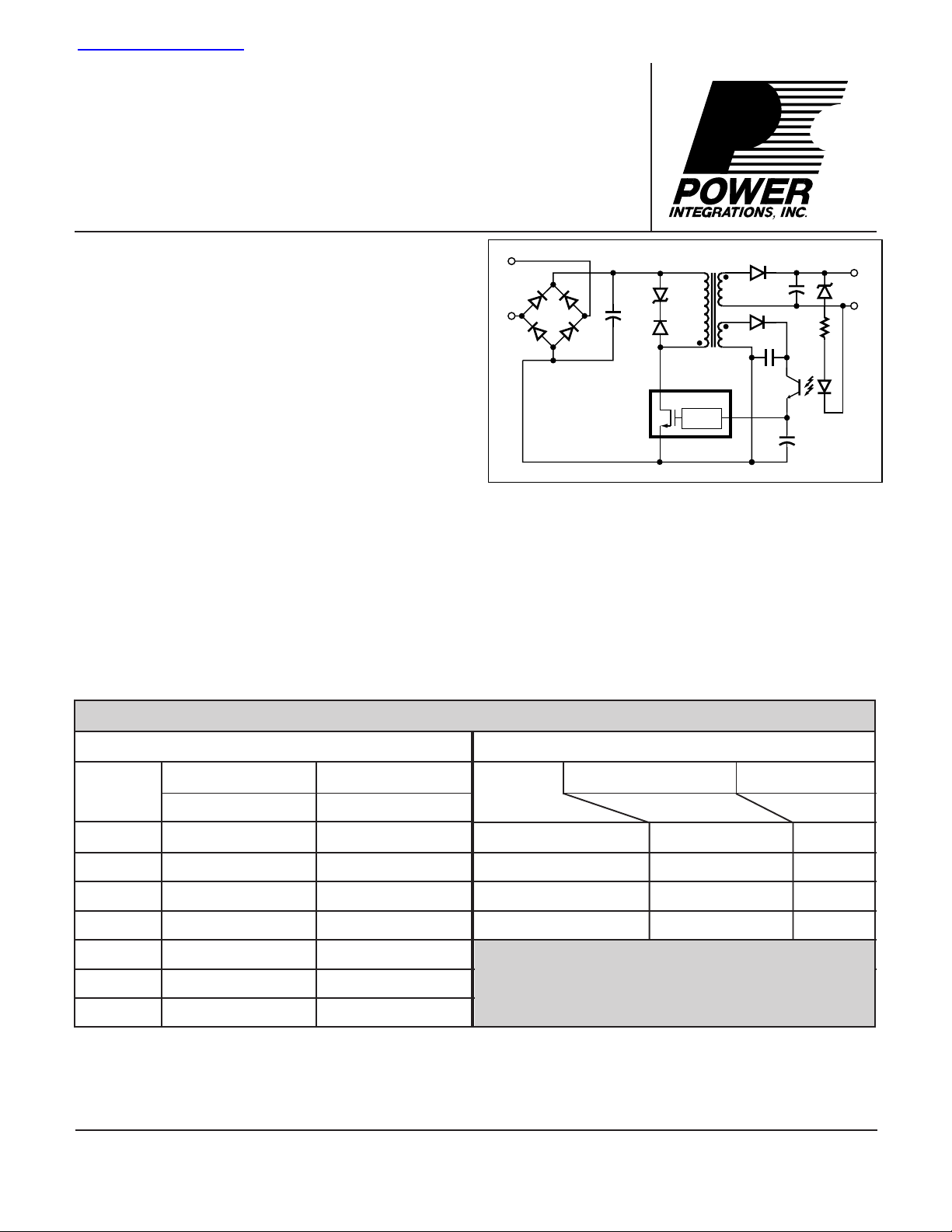
Figure 1. Typical Flyback Application.
C
PI-1951-091996
easier. The standard 8L PDIP package option reduces cost in
lower power, high efficiency applications. The internal lead
frame of this package uses six of its pins to transfer heat from
the chip directly to the board, eliminating the cost of a heat sink.
TOPSwitch incorporates all functions necessary for a switched
mode control system into a three terminal monolithic IC: power
MOSFET, PWM controller, high voltage start up circuit, loop
compensation and fault protection circuitry.
8L PDIP (P) or 8L SMD (G) Package
PART
ORDER
Single Voltage Input
100/115/230 VAC
NUMBER
TOP221P or TOP221G
.
P
±15%
MAX
9 W
3
Wide Range Input
5,6
2
85 to 265 VAC
P
MAX
6 W
5,6
TOP222Y
TOP223Y
TOP224Y
TOP225Y
TOP226Y
TOP227Y
25 W
50 W
75 W
100 W
125 W
150 W
15 W
30 W
45 W
60 W
75 W
90 W
TOP222P or TOP222G
TOP223P or TOP223G
TOP224P or TOP224G
15 W
25 W
30 W
10 W
15 W
20 W
Notes: 1. Package outline: TO-220/3 2. Package Outline: DIP-8 or SMD-8 3. 100/115 VAC with doubler input 4. Assumes appropriate
heat sinking to keep the maximum TOPSwitch junction temperature below 100 °C. 5. Soldered to 1 sq. in.( 6.45 cm2), 2 oz. copper clad
(610 gm/m2) 6. P
in a given application depends on thermal environment, transformer design, efficiency required, minimum specified input voltage, input
is the maximum practical continuous power output level for conditions shown. The continuous power capability
MAX
storage capacitance, etc. 7. Refer to key application considerations section when using TOPSwitch-II in an existing TOPSwitch design.
July 2001
TOP221-227
PI-2084-040401
CONTROL
DRAIN
SOURCE
Y Package (TO-220/3)
Tab Internally
Connected to SOURCE Pin
CONTROL
8
5
7
6
DRAIN
SOURCE (HV RTN)
SOURCE
SOURCE
1
4
2
3
SOURCE (HV RTN)
SOURCE (HV RTN)
SOURCE
P Package (DIP-8)
G Package (SMD-8)
CONTROL
Z
C
SHUNT REGULATOR/
ERROR AMPLIFIER
I
FB
OSCILLATOR
R
E
V
C
D
MAX
CLOCK
SAW
0
INTERNAL
SUPPLY
POWER-UP
RESET
1
÷ 8
+
-
V
I
MINIMUM
ON-TIME
DELAY
LIMIT
SRQ
Q
SRQ
CONTROLLED
TURN-ON
GATE
DRIVER
LEADING
Q
EDGE
BLANKING
SHUTDOWN/
AUTO-RESTART
+
5.7 V
5.7 V
4.7 V
THERMAL
SHUTDOWN
COMPARATOR
+
-
+
PWM
DRAIN
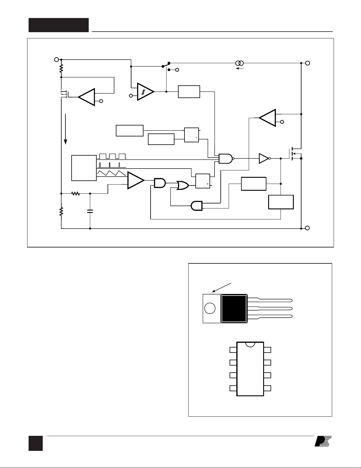
Figure 2. Functional Block Diagram.
Pin Functional Description
DRAIN Pin:
Output MOSFET drain connection. Provides internal bias
current during start-up operation via an internal switched highvoltage current source. Internal current sense point.
CONTROL Pin:
Error amplifier and feedback current input pin for duty cycle
control. Internal shunt regulator connection to provide internal
bias current during normal operation. It is also used as the
connection point for the supply bypass and auto-restart/
compensation capacitor.
SOURCE Pin:
Y package – Output MOSFET source connection for high
voltage power return. Primary side circuit
common and reference point.
SOURCE
PI-1935-091696
P and G package – Primary side control circuit common and
reference point.
SOURCE (HV RTN) Pin: (P and G package only)
Output MOSFET source connection for high voltage power return.
D
2
7/01
Figure 3. Pin Configuration.
TOP221-227
TOPSwitch-II
Family Functional Description
TOPSwitch is a self biased and protected linear control currentto-duty cycle converter with an open drain output. High
efficiency is achieved through the use of CMOS and integration
of the maximum number of functions possible. CMOS process
significantly reduces bias currents as compared to bipolar or
discrete solutions. Integration eliminates external power
resistors used for current sensing and/or supplying initial startup bias current.
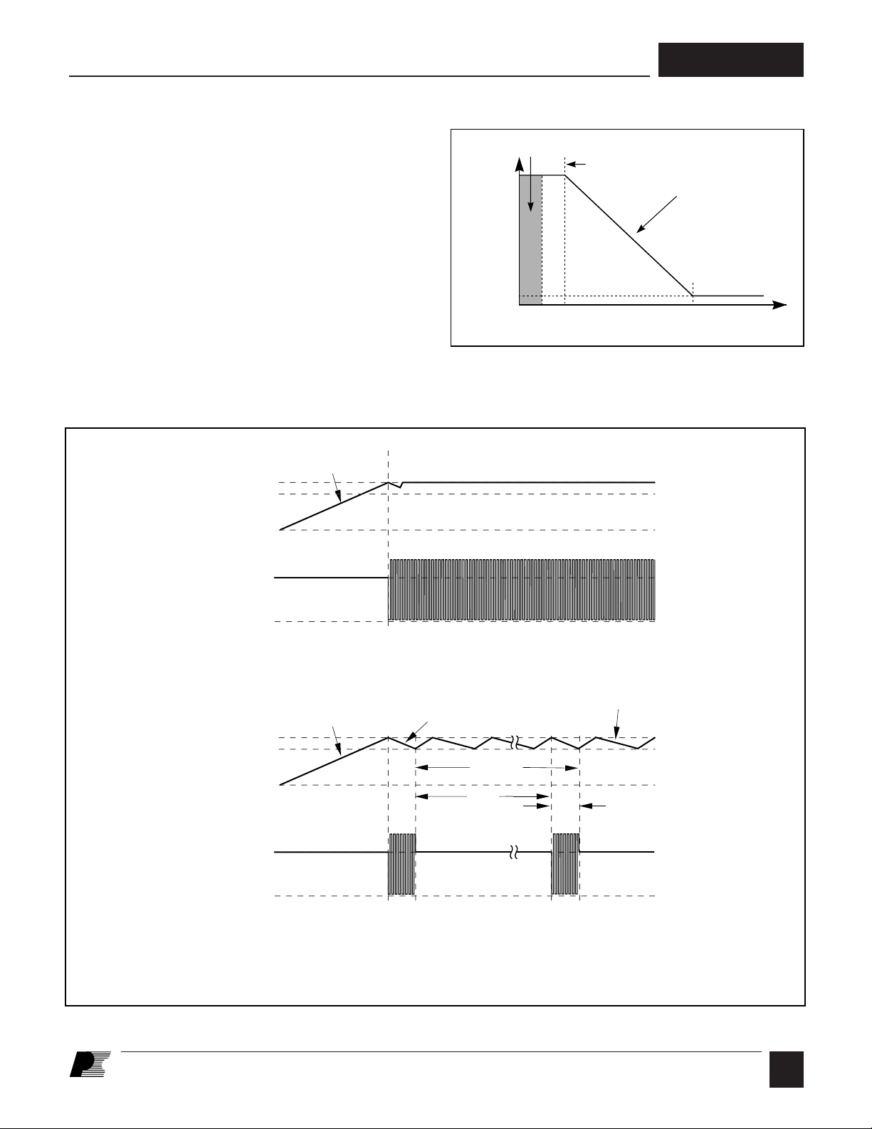
During normal operation, the duty cycle of the internal output
MOSFET decreases linearly with increasing CONTROL pin
current as shown in Figure 4. To implement all the required
control, bias, and protection functions, the DRAIN and
CONTROL pins each perform several functions as described
below. Refer to Figure 2 for a block diagram and to Figure 6 for
timing and voltage waveforms of the TOPSwitch integrated
circuit.
I
C
5.7 V
Charging C
4.7 V
V
C
T
0
Auto-restart
I
D
MAX
Duty Cycle (%)
D
MIN
I
CD1
Figure 4. Relationship of Duty Cycle to CONTROL Pin Current.
B
Slope = PWM Gain
2.0 6.0
IC (mA)
PI-2040-050197
DRAIN
V
DRAIN
C
V
IN
5.7 V
4.7 V
V
IN
Off
0
(a)
I
Discharging C
95%
Off
0
0
I
C
Charging C
Off
T
Switching Switching
(b)
CT is the total external capacitance
connected to the CONTROL pin
Switching
CD1
8 Cycles
I
CD2
Discharging C
T
5%
T
Off
PI-1956-092496
Figure 5. Start-up Waveforms for (a) Normal Operation and (b) Auto-restart.
7/01
D
3

TOP221-227
TOPSwitch-II
Family Functional Description (cont.)
Control Voltage Supply
CONTROL pin voltage VC is the supply or bias voltage for the
controller and driver circuitry. An external bypass capacitor
closely connected between the CONTROL and SOURCE pins
is required to supply the gate drive current. The total amount
of capacitance connected to this pin (C
) also sets the auto-
T
restart timing as well as control loop compensation. VC is
regulated in either of two modes of operation. Hysteretic
regulation is used for initial start-up and overload operation.
Shunt regulation is used to separate the duty cycle error signal
from the control circuit supply current. During start-up,
CONTROL pin current is supplied from a high-voltage switched
current source connected internally between the DRAIN and
CONTROL pins. The current source provides sufficient current
to supply the control circuitry as well as charge the total
external capacitance (CT).
The first time VC reaches the upper threshold, the high-voltage
current source is turned off and the PWM modulator and output
transistor are activated, as shown in Figure 5(a). During normal
operation (when the output voltage is regulated) feedback
control current supplies the VC supply current. The shunt
regulator keeps VC at typically 5.7 V by shunting CONTROL
pin feedback current exceeding the required DC supply current
through the PWM error signal sense resistor RE. The low
dynamic impedance of this pin (ZC) sets the gain of the error
amplifier when used in a primary feedback configuration. The
dynamic impedance of the CONTROL pin together with the
external resistance and capacitance determines the control loop
compensation of the power system.
If the CONTROL pin total external capacitance (CT) should
discharge to the lower threshold, the output MOSFET is turned
off and the control circuit is placed in a low-current standby
mode. The high-voltage current source turns on and charges the
external capacitance again. Charging current is shown with a
negative polarity and discharging current is shown with a
positive polarity in Figure 6. The hysteretic auto-restart
comparator keeps VC within a window of typically 4.7 to 5.7 V
by turning the high-voltage current source on and off as shown
in Figure 5(b). The auto-restart circuit has a divide-by-8
counter which prevents the output MOSFET from turning on
again until eight discharge-charge cycles have elapsed. The
counter effectively limits TOPSwitch power dissipation by
reducing the auto-restart duty cycle to typically 5%. Autorestart continues to cycle until output voltage regulation is
again achieved.
Bandgap Reference
All critical TOPSwitch internal voltages are derived from a
temperature-compensated bandgap reference. This reference
is also used to generate a temperature-compensated current
source which is trimmed to accurately set the oscillator frequency
and MOSFET gate drive current.
D
4
7/01
Oscillator
The internal oscillator linearly charges and discharges the
internal capacitance between two voltage levels to create a
sawtooth waveform for the pulse width modulator. The oscillator
sets the pulse width modulator/current limit latch at the beginning
of each cycle. The nominal frequency of 100 kHz was chosen
to minimize EMI and maximize efficiency in power supply
applications. Trimming of the current reference improves the
frequency accuracy.
Pulse Width Modulator
The pulse width modulator implements a voltage-mode control
loop by driving the output MOSFET with a duty cycle inversely
proportional to the current into the CONTROL pin which
generates a voltage error signal across RE. The error signal
across RE is filtered by an RC network with a typical corner
frequency of 7 kHz to reduce the effect of switching noise. The
filtered error signal is compared with the internal oscillator
sawtooth waveform to generate the duty cycle waveform. As
the control current increases, the duty cycle decreases. A clock
signal from the oscillator sets a latch which turns on the output
MOSFET. The pulse width modulator resets the latch, turning
off the output MOSFET. The maximum duty cycle is set by the
symmetry of the internal oscillator. The modulator has a
minimum ON-time to keep the current consumption of the
TOPSwitch independent of the error signal. Note that a minimum
current must be driven into the CONTROL pin before the duty
cycle begins to change.
Gate Driver
The gate driver is designed to turn the output MOSFET on at a
controlled rate to minimize common-mode EMI. The gate drive
current is trimmed for improved accuracy.
Error Amplifier
The shunt regulator can also perform the function of an error
amplifier in primary feedback applications. The shunt regulator
voltage is accurately derived from the temperature compensated
bandgap reference. The gain of the error amplifier is set by the
CONTROL pin dynamic impedance. The CONTROL pin
clamps external circuit signals to the VC voltage level. The
CONTROL pin current in excess of the supply current is
separated by the shunt regulator and flows through RE as a
voltage error signal.
Cycle-By-Cycle Current Limit
The cycle by cycle peak drain current limit circuit uses the
output MOSFET ON-resistance as a sense resistor. A current
limit comparator compares the output MOSFET ON-state drainsource voltage, V
current causes V
with a threshold voltage. High drain
DS(ON)
to exceed the threshold voltage and turns
DS(ON)
the output MOSFET off until the start of the next clock cycle.
The current limit comparator threshold voltage is temperature
V
IN
DRAIN
V
OUT
I
OUT
TOP221-227
V
IN
0
0
0
12 12 81
V
C
0
12
I
0
C
1 2
Figure 6. Typical Waveforms for (1) Normal Operation, (2) Auto-restart, and (3) Power Down Reset.
compensated to minimize variation of the effective peak current
limit due to temperature related changes in output MOSFET
R
.
DS(ON)
8
• • ••
812 81
• • ••
•
•
•
•
becomes regulated, VC regulation returns to shunt mode, and
normal operation of the power supply resumes.
Overtemperature Protection
The leading edge blanking circuit inhibits the current limit
comparator for a short time after the output MOSFET is turned
on. The leading edge blanking time has been set so that current
spikes caused by primary-side capacitances and secondary-side
rectifier reverse recovery time will not cause premature
termination of the switching pulse.
Temperature protection is provided by a precision analog
circuit that turns the output MOSFET off when the junction
temperature exceeds the thermal shutdown temperature
(typically 135 °C). Activating the power-up reset circuit by
removing and restoring input power or momentarily pulling the
CONTROL pin below the power-up reset threshold resets the
latch and allows TOPSwitch to resume normal power supply
The current limit can be lower for a short period after the leading
edge blanking time as shown in Figure 12. This is due to
dynamic characteristics of the MOSFET. To avoid triggering
operation. VC is regulated in hysteretic mode and a 4.7 V to
5.7 V (typical) sawtooth waveform is present on the CONTROL
pin when the power supply is latched off.
the current limit in normal operation, the drain current waveform
should stay within the envelope shown.
High-voltage Bias Current Source
This current source biases TOPSwitch from the DRAIN pin and
Shutdown/Auto-restart
To minimize TOPSwitch power dissipation, the shutdown/
auto-restart circuit turns the power supply on and off at an autorestart duty cycle of typically 5% if an out of regulation
condition persists. Loss of regulation interrupts the external
current into the CONTROL pin. VC regulation changes from
shunt mode to the hysteretic auto-restart mode described above.
When the fault condition is removed, the power supply output
charges the CONTROL pin external capacitance (CT) during
start-up or hysteretic operation. Hysteretic operation occurs
during auto-restart and overtemperature latched shutdown.
The current source is switched on and off with an effective duty
cycle of approximately 35%. This duty cycle is determined by
the ratio of CONTROL pin charge (IC) and discharge currents
(I
CD1
and I
). This current source is turned off during normal
CD2
operation when the output MOSFET is switching.
V
C(reset)
131
PI-2030-042397
7/01
D
5
TOP221-227
L1
3.3 µH
100 µF
R2
100 Ω
+
47 kΩ
Wide-Range
DC Input
-
R3
D1
UF4005
D
S
C1
2.2 nF
1 kV
U1
TOP221P
CONTROL
T1
TOPSwitch-II
C
D2
UF5401
330 µF
C2
10 V
D3
1N4148
C4
100 µF
16 V
C5
47 µF
10 V
VR1
R1
10 Ω
U2
PC817A
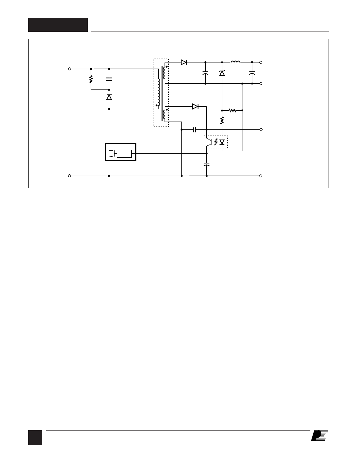
Figure 7. Schematic Diagram of a 4 W TOPSwitch-II Standby Power Supply using an 8 lead PDIP.
Application Examples
+5 V
C3
10 V
RTN
+
12 V Non-Isolated
-
PI-2115-040401
Following are just two of the many possible TOPSwitch
implementations. Refer to the Data Book and Design Guide
for additional examples.
4 W Standby Supply using 8 Lead PDIP
Figure 7 shows a 4 W standby supply. This supply is used in
appliances where certain standby functions (e.g. real time
clock, remote control port) must be kept active even while the
main power supply is turned off.
The 5 V secondary is used to supply the standby function and
the 12 V non-isolated output is used to supply power for the
PWM controller of the main power supply and other primary
side functions.
For this application the input rectifiers and input filter are sized
for the main supply and are not shown. The input DC rail may
vary from 100 V to 380 V DC which corresponds to the full
universal AC input range. The TOP221 is packaged in an 8 pin
power DIP package.
The output voltage (5 V) is directly sensed by the Zener diode
(VR1) and the optocoupler (U2). The output voltage is determined
by the sum of the Zener voltage and the voltage drop across the
LED of the optocoupler (the voltage drop across R1 is negligible).
The output transistor of the optocoupler drives the CONTROL
pin of the TOP221. C5 bypasses the CONTROL pin and provides
control loop compensation and sets the auto-restart frequency.
The transformer’s leakage inductance voltage spikes are snubbed
by R3 and C1 through diode D1. The bias winding is rectified
and filtered by D3 and C4 providing a non-isolated 12 V output
which is also used to bias the collector of the optocoupler’s
output transistor. The isolated 5 V output winding is rectified by
D2 and filtered by C2, L1 and C3.
D
6
7/01
 Loading...