Page 1

ORDER NO.
RRV1916
STEREO CD CASSETTE DECK RECEIVER
XR-A100
XR-A100-K
Refer to the service manual RRV1883 for XR-A100-K/KCXJ .
THIS MANUAL IS APPLICABLE TO THE FOLLOWING MODEL(S) AND TYPE(S).
Type
XR-A100 XR-A100-K
MYXK ‡‡AC220–230V
NVXK ‡‡AC230V
YPWXJ ‡ –– AC240V
Model
CONTENTS
1. SAFETY INFORMATION
2. CONTRAST OF MISCELLANEOUS PARTS
3. SCHEMATIC DIAGRAM
4. PCB CONNECTION DIAGRAM
5. ADJUSTMENT
....................................................
Power Requirement
......................................
.....................................
..........................
........
Remarks
2
3
10
19
27
PIONEER ELECTRONIC CORPORATION 4-1, Meguro 1-Chome, Meguro-ku, Tokyo 153-8654, Japan
PIONEER ELECTRONICS SERVICE, INC. P.O. Box 1760, Long Beach, CA 90801-1760, U.S.A.
PIONEER ELECTRONIC (EUROPE) N.V. Haven 1087, Keetberglaan 1, 9120 Melsele, Belgium
PIONEER ELECTRONICS ASIACENTRE PTE. LTD. 501 Orchard Road, #10-00 Lane Crawford Place, Singapore 0923
PIONEER ELECTRONIC CORPORATION 1998
T – DZK FEB. 1998 Printed in Japan
Page 2

XR-A100, XR-A100-K
1. SAFETY INFORMATION
This service manual is intended for qualified service technicians; it is not meant for the casual
do-it-yourselfer. Qualified technicians have the necessary test equipment and tools, and have been
trained to properly and safely repair complex products such as those covered by this manual.
Improperly performed repairs can adversely affect the safety and reliability of the product and may
void the warranty . If you are not qualified to perform the repair of this product properly and safely, you
should not risk trying to do so and refer the repair to a qualified service technician.
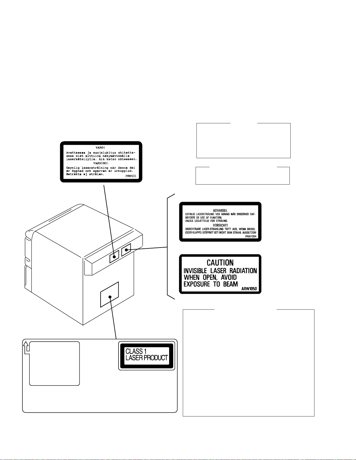
LABEL CHECK
MYXK Type
THIS PIONEER APPARATUS CONTAINS
IMPORTANT
LASER OF CLASS 1.
SERVICING OPERATION OF THE APPARATUS
SHOULD BE DONE BY A SPECIALLY
INSTRUTED PERSON.
LASER DIODE CHARACTERISTICS
MAXIMUM OUTPUT POWER: 5 mw
WAVELENGTH: 780 – 785 nm
MYXK Type
NVXK Type
Additional Laser Caution
1.Laser Interlock Mechanism
The position of the switch (S8501) for detecting loading
state is detected by the system microprocessor, and
the design prevents laser diode oscillation when the
switch (S8501) is pressed physically.
Thus, the interlock will no longer function if the switch (S8501)
is released physically and deliberatery.
The interlock also does not function in the test mode ∗.
Laser diode oscillation will continue, if pin 62 of
LA9240ML (IC8101) on the CD ASSY mounted on the
$M Loading Mechanism assembly is connected to GND,
or else the terminals of Q8101 are shorted to each other
(fault condition).
2.When the cover is opened, close viewing of the
Name Label
MYXK, NVXK and YPWXJ Types
objective lens with the naked eye will cause exposure
to a Class 1 laser beam.
∗
: Refer to page 52 on the service manual RRV1883.
2
Page 3

XR-A100, XR-A100-K
2. CONTRAST OF MISCELLANEOUS PARTS
NOTES:•Parts marked by "NSP" and ⊗ can not be supplied.
The mark found on some component parts indicates the importance of the safety factor of the part.
•
Therefore, when replacing, be sure to use parts of identical designation.
When ordering resistors, first convert resistance values into code form as shown in the following examples.
•
Ex.1 When there are 2 effective digits (any digit apart from 0), such as 560 ohm and 47k ohm (tolerance is shown by J=5%,
and K=10%).
560 Ω→56 × 10
47k Ω→47 × 103→ 473 ........................................................ RD1/4PU 4 7 3 J
0.5 Ω→R50 ..................................................................................... RN2H
1 Ω→1R0 ..................................................................................... RS1P
Ex.2 When there are 3 effective digits (such as in high precision metal film resistors).
5.62k Ω→ 562 × 10
Reference Nos. indicate the pages and Nos. in the service manual for the base model.
•
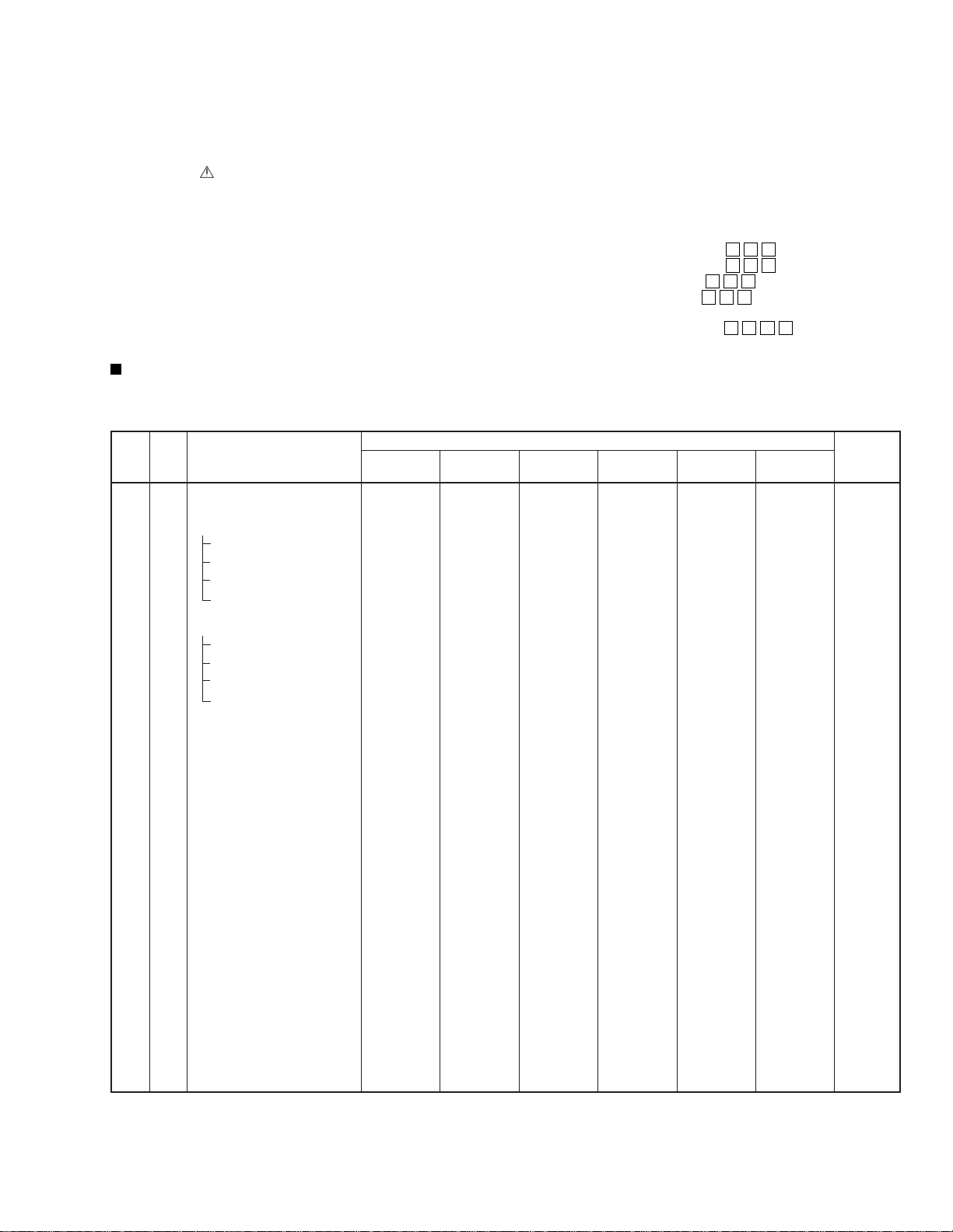
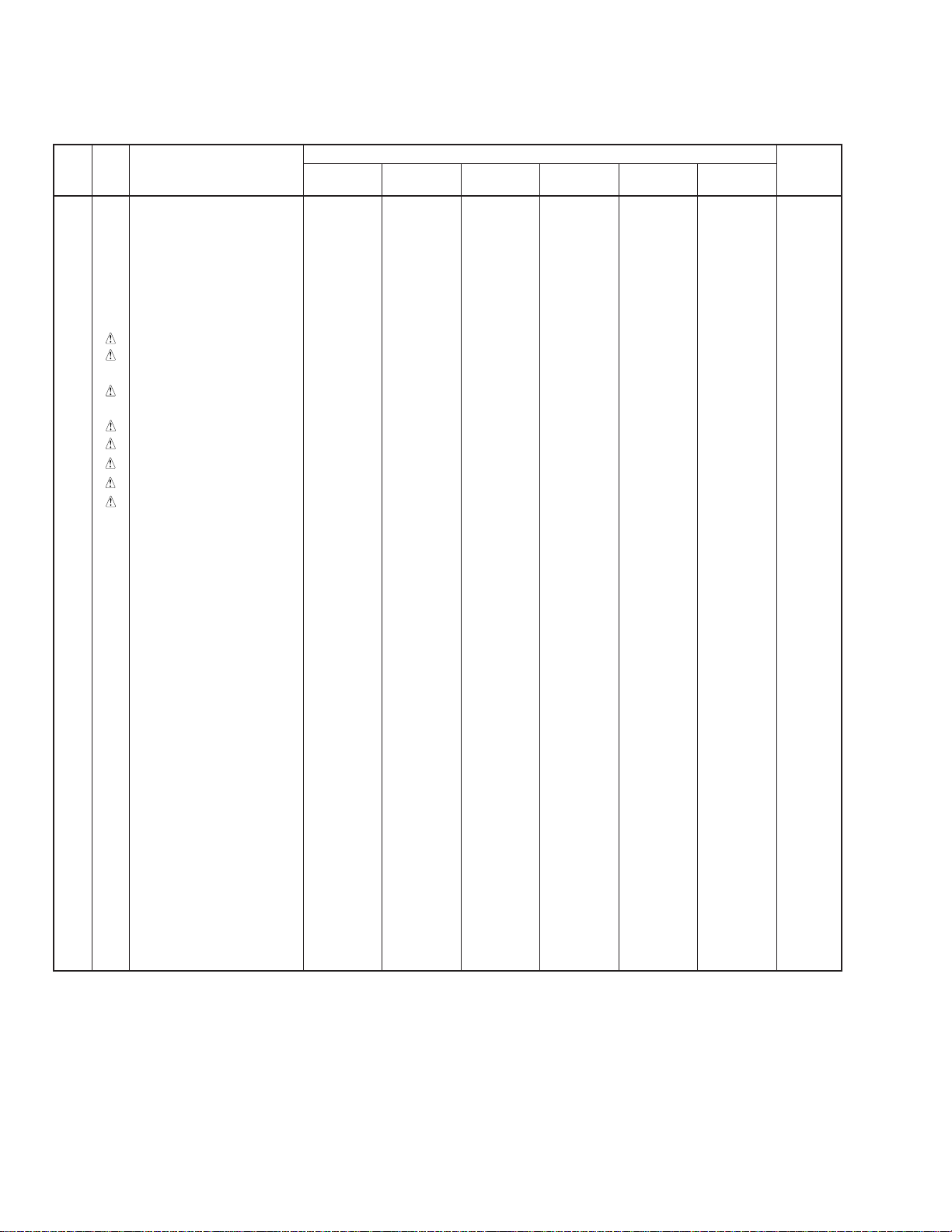
CONTRAST TABLE
XR-A100/MYXK, NVXK, YPWXJ, XR-A100-K/MYXK, NVXK and XR-A100-K/KCXJ are constructed the same
except for the following :
1
→ 561 ........................................................ RD1/4PU 5 6 1 J
R 5 0
1 R 0
1
→ 5621 ......................................................RN1/4PC 5 6 2 1 F
K
K
.feR
kraMnoitpircseDdnalobmyS
.oN
1-7P ⊗ yssAFA4003MWX7003MWX7003MWX1003MWX7003MWX7003MWX *1
PSNyssAYLPPUSREWOP5003MWX0627MWA0627MWA3827MWA0627MWA0627MWA
2-7P ⊗ yssASNART0103ZWX7458ZWA7458ZWA8358ZWA7458ZWA7458ZWA *1
3-7P ⊗ yssAREWOP1103ZWX8458ZWA8458ZWA4358ZWA8458ZWA8458ZWA *1
92-7P ⊗ 2yssAREWOP2103ZWXdesutoNdesutoNdesutoNdesutoNdesutoN
03-7P ⊗ yssA2SNART3103ZWXdesutoNdesutoNdesutoNdesutoNdesutoN
PSNyssAXELPMOC6003MWX8003MWX8003MWX2003MWX8003MWX8003MWX
1-9P ⊗ yssAKCED7003ZWX7103ZWX7103ZWX2003ZWX7103ZWX7103ZWX
4-9P ⊗ yssAYALPSID4103ZWX6103ZWX6103ZWX1003ZWX6103ZWX6103ZWX
5-9P ⊗ yssADCL5103ZWX8103ZWX8103ZWX6003ZWX8103ZWX8103ZWX
6-9P ⊗ yssAPMAL8003ZWX4203ZWX4203ZWX8003ZWX4203ZWX4203ZWX
4-7P ⊗ ELUDOMRENUTMA/MF1607QXA
1-3PannetnAMF4007HDA5007HDA5007HDA4007HDA5007HDA5007HDA
2-3PsnoitcurtsnIgnitarepO5003ERXdesutoNdesutoN5003ERXdesutoNdesutoN
)hsinapS/hcnerF/hsilgnE(
snoitcurtsnIgnitarepOdesutoN1003CRXdesutoNdesutoN1003CRXdesutoN
)hctuD/namreG/hcnerF(
snoitcurtsnIgnitarepOdesutoN2003CRXdesutoNdesutoN2003CRXdesutoN
)naissuR/hsidewS/nailatI(
snoitcurtsnIgnitarepOdesutoN6003ERXdesutoNdesutoN6003ERXdesutoN
)eseugutroP/hsinapS/hsilgnE(
)hsilgnE(snoitcurtsnIgnitarepOdesutoNdesutoN1003BRXdesutoNdesutoN1003BRX
K-001A-RX
JXCK/
001A-RX
KXYM/
*2
7707QXA
KXVN/
7707QXA
.oNtraP
001A-RX
*2
001A-RX
JXWPY/
1607QXA
K-001A-RX
KXYM/
*2
7707QXA
K-001A-RX
KXVN/
*2
7707QXA
skrameR
3-3PannetnApooLMA1003BTX7007BTA7007BTA1003BTX7007BTA7007BTA
4-3PtinUlortnoCetomeR2003NZX2003NZX2003NZXdesutoN2003NZX2003NZX
)040RX-UC(
4-3PtinUlortnoCetomeRdesutoNdesutoNdesutoN3003NZXdesutoNdesutoN
)930RX-UC(
01-3PesaCgnikcaP8003DHX0103DHX0103DHX7003DHX1303DHX1303DHX
11-3PteehSgnikcaP3007GHA1007GHA1007GHA3007GHA1007GHA1007GHA
Notes *1 : Refer to “PCB PARTS LIST” , “3. SCHEMATIC DIAGRAM” and “4. PCB CONNECTION DIAGRAM”.
*2 : Refer to “PCB PARTS LIST” , “3. SCHEMATIC DIAGRAM” , “4. PCB CONNECTION DIAGRAM” and “5. ADJUSTMENT”.
3
Page 4

XR-A100, XR-A100-K
.feR
kraMnoitpircseDdnalobmyS
.oN
21-3PPSNdraCytnarraW5701YRA0107YRA0107YRA3001YRP0107YRA0107YRA
6-5PpaCyarT6103KAX8003KAX8003KAX8003KAX6103KAX6103KAX
7-5PlenaPyalpsiD5003KAX5003KAX5003KAX3003KAX5003KAX5003KAX
8-5PesaCtennoB5003NZX1003NZX1003NZX1003NZX5003NZX5003NZX
31-5PPSNlebaL56&PCI1257XAAdesutoNdesutoNdesutoNdesutoNdesutoN
13-7PreirraBCVP4707CEA9207KNA9207KNA9207KNA9207KNA9207KNA
5-7P)V021CA(remrofsnarTrewoP4003STXdesutoNdesutoNdesutoNdesutoNdesutoN
5-7PremrofsnarTrewoPdesutoN2417STA2417STAdesutoN2417STA2417STA
)V032-022CA(
5-7P)V042CA(remrofsnarTrewoPdesutoNdesutoNdesutoN9317STAdesutoNdesutoN
6-7P)1UF,A51.3(esuF1801KERdesutoNdesutoNdesutoNdesutoNdesutoN
6-7P)1UF,A1T(esuFdesutoN4501KEA4501KEAdesutoN4501KEA4501KEA
6-7P)1UF,A1(esuFdesutoNdesutoNdesutoN2201KERdesutoNdesutoN
7-7PdroCrewoPCA7501GDP8007GDA7007GDA9511GDA8007GDA7007GDA
)gulPCAnihtiW()A5T(esuFdesutoNdesutoN1007KEAdesutoNdesutoN1007KEA
01-7PetalPDNG6017GNA1317GNA1317GNA6017GNA1317GNA1317GNA
21-7PetalPdleihS2317GNA8117GNA8117GNA8117GNA8117GNA8117GNA
31-7PkniStaeH3607HNA7407HNA7407HNA9507HNA7407HNA7407HNA
51-7PrevoCraeR1107CMA3007CMA3007CMA3007CMA3007CMA3007CMA
61-7PfeileRniartSC22-MCB22-MCB22-MCB22-MCB22-MCB22-MC
K-001A-RX
JXCK/
001A-RX
KXYM/
KXVN/
.oNtraP
001A-RX
001A-RX
JXWPY/
K-001A-RX
KXYM/
K-001A-RX
skrameR
KXVN/
62-7PPSNlebaLemaN9003XAX2103XAX1103XAX8003XAX2603XAX4603XAX
82-7PCtekcarB7217GNAdesutoNdesutoNdesutoNdesutoNdesutoN
32-9PPSNyssAlenaPtnorF8003GXX6003GXX6003GXX2003GXX0103GXX0103GXX
42-9PnottuBnoitcnuF4003DAX1003DAX1003DAX1003DAX4003DAX4003DAX
03-9PLtekcoProoD3003NAX1003NAX1003NAX1003NAX3003NAX3003NAX
13-9PRtekcoProoD4003NAX2003NAX2003NAX2003NAX4003NAX4003NAX
23-9PlenaPtnorF8003BMX6003BMX6003BMX2003BMX0103BMX0103BMX
BlebaLCOD5861WRDdesutoNdesutoNdesutoNdesutoNdesutoN
AtekcarBdesutoN0017GNA0017GNA0017GNA0017GNA0017GNA * 1.oN,3
)AtekcarBrof(wercSdesutoN
)etalPdleihSrof(wercSdesutoN
roticapaCcimareCdesutoN
EHlebaLnoituaCdesutoN3321WRPdesutoNdesutoN3321WRPdesutoN *5
lebaLnoituaCdesutoN4901WRVdesutoNdesutoN4901WRVdesutoN *5
PSNlebaLnoituaCdesutoNdesutoN0501WRAdesutoNdesutoN0501WRA *5
bonKCIMdesutoNdesutoNdesutoN1003BAXdesutoNdesutoN *6
BCZ4 F060P0KZ BCZ4 F060P0KZ BCZ4 F060P0KZ BCZ4 F060P0KZ BCZ4 F060P0KZ
CMF021P03ZBBCMF021P03ZBBCMF021P03ZBBCMF021P03ZBBCMF021P03ZBB
05K221BYCKC05K221BYCKC
desutoN
Notes *3 : The numbers in the remarks column correspond to the numbers on the “EXPLODED VIEWS”.
*4 : Solder to the FM/AM TUNER MODULE and the GND Plate (ANG7131).
*5 : Refer to page 2.
*6 : For MIC LEVEL control (DISPLAY ASSY : VR2501).
05K221BYCKC05K221BYCKC
* 2.oN,3
* 3.oN,3
*4
4
Page 5

XR-A100, XR-A100-K
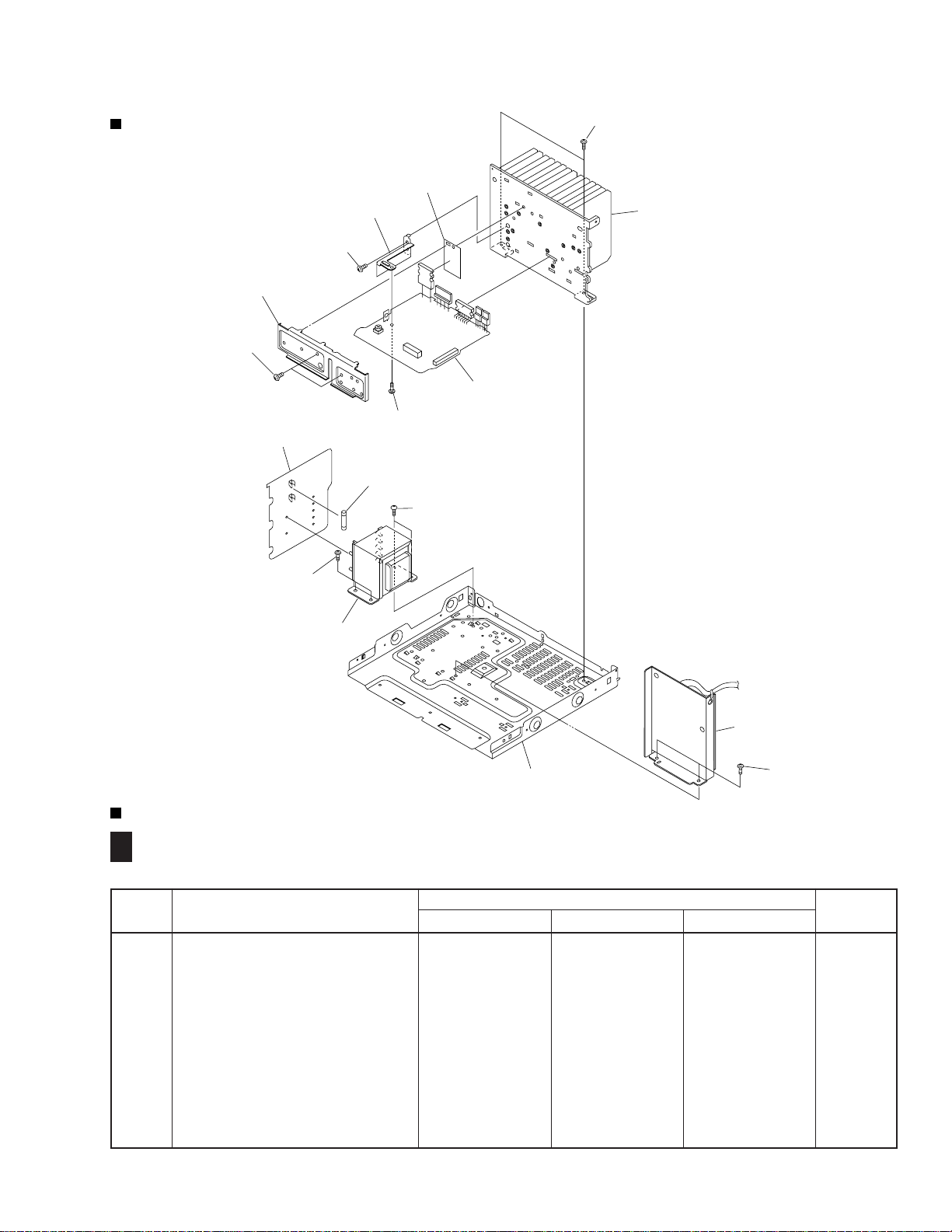
EXPLODED VIEWS
VBZ30P080FZK
1
2
TRANS ASSY
Bracket B
VBZ30P080FZK
Fuse (FU1)
VBZ30P080FZK
Mica Sheet
Heat Sink
POWER ASSY
ABA7031
ABA7031
Power Transformer
Chassis
CONTRAST OF PCB ASSEMBLIES
DECK ASSY
I F
XWZ3017, XWZ3002 and XWZ3007 are constructed the same except for the following :
kraMnoitpircseDdnalobmyS
1524LdesutoNJ001UALdesutoN
5524CdesutoN05K201BYCKCdesutoN
7524CdesutoN05M0R1TAECdesutoN
2054CdesutoN05J181LSCCCdesutoN
4054CdesutoN05J151LSCCCdesutoN
5064CdesutoN05K281BYDKCdesutoN
7003ZWX7103ZWX2003ZWX
2224C,1224C05J372ABMQC05J372ABMQC05J333ABMQC
8224C,7224C05K222BYCKC05K222BYCKC05K251BYCKC
3054C,1054CdesutoN05J181LSDCCdesutoN
2064C,1064CdesutoN05J074LSCCCdesutoN
4064C,3064CdesutoN05J101LSCCCdesutoN
.oNtraP
Shield Plate
3
skrameR
5
Page 6

XR-A100, XR-A100-K
DISPLAY ASSY
M F
XWZ3016, XWZ3001 and XWZ3014 are constructed the same except for the following :
kraMnoitpircseDdnalobmyS
1552LdesutoNdesutoNK0R1UAL
1052CdesutoNdesutoN05K133BYUPKC
4052CdesutoNdesutoN52K374XYCGC
5052CdesutoNdesutoN05M7R4AJEC
6052CdesutoNdesutoN52M033AJEC
7052CdesutoNdesutoN05J401ABMQC
4552CdesutoNdesutoN05K201BYUPKC
4052RdesutoNdesutoNJ401UP4/1DR
5052RdesutoNdesutoNJ201UP4/1DR
6052RdesutoNdesutoNJ374UP4/1DR
7052RdesutoNdesutoNJ157UP4/1DR
0152RdesutoNdesutoNJ101UP4/1DR
4103ZWX6103ZWX1003ZWX
1052CIdesutoNdesutoNDL8554MJN
5281S–1181S1501GSA4301GSA1501GSA
3021C,2021C52Z301FYUPKCdesutoN52Z301FYUPKC
2521C,1521CdesutoN52Z301FYUPKCdesutoN
8052C,3052C,2052CdesutoNdesutoN05M2R2AJEC
2021R,1021RJ133FML1SRJ151FMP2/1DRJ151FMP2/1DR
2052R,1052RdesutoNdesutoNJ233UP4/1DR
9052R,8052RdesutoNdesutoNJ301UP4/1DR
1052RVk01( Ω)desutoNdesutoN1201SCV
)KCAJCIM(2052AJ,1052AJdesutoNdesutoN4007NKA
.oNtraP
skrameR
LCD ASSY
O F
XWZ3018, XWZ3006 and XWZ3015 are constructed the same except for the following :
kraMnoitpircseDdnalobmyS
5091D452SS1desutoNdesutoN
6091DdesutoN452SS1desutoN
LAMP ASSY
N F
5103ZWX8103ZWX6003ZWX
)F740.0(3091C3107HCA6421HCA3107HCA
.oNtraP
XWZ3024 and XWZ3008 are constructed the same except for the following :
kraMnoitpircseDdnalobmyS
1481QdesutoN0651AS2
2481QdesutoN0404CS2
1481RdesutoNJ174UP4/1DR
2481RdesutoNJ274UP4/1DR
3481RdesutoNJ201UP4/1DR
5481RdesutoNJ151FML2SR
8003ZWX4203ZWX
2481D,1481DdesutoN452SS1
2091LP,1091LPdesutoN7007LEA
.oNtraP
skrameR
skrameR
6
Page 7

PCB PARTS LIST
Mark No. Description Parts No.
FM/AM TUNER MODULE (AXQ7077)
E F
SEMICONDUCTOR
IC6201 LA1832ML
IC6202 LC72131MD
Q6102 2SC2223
Q6203 2SC2705
Q6201, Q6202 2SC2712
Q6103, Q6214, Q6601 2SC2714
Q6104, Q6105 2SK302
Q6101 3SK194
Q6204 DTA124ES
Q6205 DTC124EK
D6202 1SS254
D6101–D6104 1SV228
COILS AND FILTERS
L6106 ATC1003
L6105 ATC1015
L6101 ATC1016
L6102 ATC1017
L6103 ATC1018
L6104 ATC1019
F6203 ATF–119
F6206 ATF7008
F6601 ATF7009
F6204 ATF7010
F6202 ATF7011
L6107 ATH1043
L6603 LAU220J
L6206, L6208, L6605 LAU2R2J
XR-A100, XR-A100-K
Mark No. Description Parts No.
C6227 CEAT220M50
C6236 CEAT2R2M50
C6216 CEAT330M16
C6262 CEAT3R3M50
C6219 CEAT470M10
C6244 CEAT470M16
C6249, C6250, C6265, C6266 CEAT4R7M50
C6258 CEJA470M16
C6215 CFTLA103J50
C6214 CFTLA224J50
C6115, C6125, C6126, C6211, C6254 CKSQYB102K50
C6601 CKSQYB102K50
C6102, C6114, C6121, C6123, C6124 CKSQYB103K50
C6210, C6213, C6237, C6267, C6276 CKSQYB103K50
C6279, C6281, C6604 CKSQYB103K50
C6251, C6252 CKSQYB123K50
C6606, C6607 CKSQYB182K50
C6203, C6259 CKSQYB223K50
C6228 CKSQYB472K50
C6209 CKSQYB473K50
C6230 CKSQYB821K50
C6218, C6223, C6255 CKSQYF103Z50
C6220, C6226, C6242, C6256 CKSQYF223Z50
C6225 CKSQYF473Z50
C6610 CKSYB103K50
RESISTORS
R6602 RD1/4PU221J
R6115, R6119, R6123, R6127, R6129 RS1/8S0R0J
R6906, R6909, R6911 RS1/8S0R0J
R6112 RS1/8S473J
VR6201 (10kΩ) RCP1045
TRANSFORMERS
T6201 ATB7008
T6101 ATE7002
CAPACITORS
C6113, C6212, C6274, C6275, C6611 CCSQCH101J50
C6116, C6208, C6221 CCSQCH150J50
C6222 CCSQCH180J50
C6271 CCSQCH200J50
C6117 CCSQCH330J50
C6608 CCSQCH680J50
C6118 CCSQCH8R0D50
C6111, C6122 CCSQCK1R0C50
C6112, C6127 CCSQCK2R0C50
C6105 CCSQSL471J50
C6101 CCSQTH110J50
C6119 CCSQTH150J50
C6109 CCSQTH270J50
C6107, C6110 CCSQTH300J50
C6106 CCSQTH330J50
C6234, C6235 CEAL1R0M50
C6245 CEAL470M16
C6224 CEAT100M50
C6243 CEAT101M16
C6231 CEAT1R0M50
Other Resistors RS1/10S&&&J
OTHERS
BN6202 2P TERMINAL WITH PAL AKA7001
X6202 CERAMIC RESONATOR ASS1066
X6201 CRYSTAL RESONATOR ASS1093
CN6201 14P SOCKET KP200IA14L
AF ASSY (XWM3001)
K F
(456kHz)
(7.2000MHz)
AM RF TUNING BLOCK AXX7042
SEMICONDUCTORS
IC2151 BA3837
IC2101 LC75394NED
IC1051 NJM78M12FA
Q1054 2SA1048
Q1051 2SA1560
Q1052, Q1053, Q1056, Q2161 2SC2458
Q1055 2SC4040
Q2151 DTC124ES
D2101–D2103, D2161, D2171 1SS254
D1054 MTZJ11C
7
Page 8

XR-A100, XR-A100-K
Mark No. Description Parts No. Mark No. Description Parts No.
D1053, D1056 MTZJ15A
D1055 MTZJ18B
D1051, D1052, D1057 S5688G
COILS AND FILTERS
L2101 LAU1R0J
CAPACITORS
C2123, C2124 CCCSL101J50
C2111, C2112 CEASR68M50
C1056–C1058, C2161 CEAT100M50
C1059 CEAT101M10
C2162 CEAT1R0M50
C2141 CEAT221M10
C2101–C2104, C2107–C2110 CEAT2R2M50
C2125, C2126, C2151, C2152, C2156 CEAT2R2M50
C2163 CEAT2R2M50
C2153 CEAT330M25
C2121, C2122, C2142 CEAT470M25
C2255 CKCYB102K50
C1062, C1063, C1067, C1070 CKCYB152K50
C2171, C2172, C2184, C2260 CKCYB152K50
C1053 CKCYB222K50
C1055 CKCYB471K50
C1052, C1054, C2119, C2120 CKCYB472K50
C2131, C2132 CKCYB682K50
C2155 CQMA224J50
C2117, C2118 CQMBA222J50
C2113, C2114 CQMBA393J50
C2154 CQMBA473J50
C2115, C2116 CQMBA563J50
D1051, D1052, D1057 S5688G
COILS AND FILTERS
L1051–L1054 (5.3µH) ATH-059
L2101 LAU1R0J
CAPACITORS
C1061, C1064, C1068, C1069 CCCSL101J50
C2123, C2124, C2180, C2182 CCCSL101J50
C1056–C1058, C2161 CEAT100M50
C1059 CEAT101M10
C2162 CEAT1R0M50
C2141 CEAT221M10
C2101–C2104, C2107–C2109 CEAT2R2M50
C2125, C2126, C2134, C2163 CEAT2R2M50
C2121, C2122, C2142 CEAT470M25
C2111, C2112 CEATR47M50
C2170, C2255 CKCYB102K50
C1062, C1063, C1067, C1070 CKCYB152K50
C2171, C2172, C2181, C2183, C2184 CKCYB152K50
C2260 CKCYB152K50
C1053 CKCYB222K50
C1055, C2127, C2128 CKCYB471K50
C1052, C1054, C2119, C2120 CKCYB472K50
C2131, C2132 CKCYB682K50
C2117, C2118 CQMBA222J50
C2113–C2116 CQMBA563J50
RESISTORS
R1062–R1065 RD1/4LMF101J
Other Resistors RD1/4PU&&&J
RESISTORS
All Resistors RD1/4PU&&&J
OTHERS
CN1201 SPEAKER TERMINAL 4–P AKE7035
CN1052 FFC CONNECTOR 20P HLEM20R-1
CN1053 FFC CONNECTOR 40P HLEM40S-1
CN1054 14P PLUG KM200IB14
CN1051 17P PLUG KM200TA17
JA2101 2P PIN JACK VKB1050
AF ASSY (XWM3007)
K F
SEMICONDUCTORS
IC2101 LC75394NED
IC1051 NJM78M12FA
Q1054 2SA1048
Q1051 2SA1560
Q1052, Q1053, Q1056, Q2161 2SC2458
Q1055 2SC4040
D2101–D2103, D2161, D2171 1SS254
D1054 MTZJ11C
D1053, D1056 MTZJ15A
D1055 MTZJ18B
OTHERS
CN1201 SPEAKER TERMINAL 4–P AKE7035
CN1052 FFC CONNECTOR 20P HLEM20R-1
CN1053 FFC CONNECTOR 40P HLEM40S-1
CN1054 14P PLUG KM200IB14
CN1051 17P PLUG KM200TA17
JA2101 2P PIN JACK VKB1050
TRANS ASSY
A F
(1) CONTRAST TABLE
AWZ8547 and AWZ8538 are constructed the same except
for the following :
Mark
Symbol and
Description
L101 ATF-151 Not used
C102 ACG7020 Not used
H103, H104 AKR1003 AKR1004
AWZ8547 AWZ8538
Part No.
Remarks
(2) PARTS LIST FOR AWZ8547
COILS AND FILTERS
L101 ATF-151
CAPACITORS
C102 (10000pF/250V) ACG7020
C101 CEANP1R0M50
8
Page 9

XR-A100, XR-A100-K
Mark No. Description Parts No. Mark No. Description Parts No.
RESISTORS
R101 RF1/4PS100J
OTHERS
H103, H104 FUSE CLIP AKR1003
POWER ASSY
C F
TERMINAL RKC-061
(1) CONTRAST TABLE
AWZ8548 and AWZ8534 are constructed the same except
for the following :
Mark
Symbol and
Description
C1094–C1097 CKCYB102K50 Not used
C1201, C1202 CKCYB102K50 CKCYB222K50
C1203, C1204 CEASR47M50 CEASR10M50
C1205 CFTYA473J50 CKCYF473Z50
AWZ8548 AWZ8534
Part No.
Remarks
(2) PARTS LIST FOR AWZ8548
SEMICONDUCTORS
IC1003, IC1202 PROTECTOR AEK7004
IC1004 PROTECTOR (1A/125V) AEK7009
IC1005 PROTECTOR (2A/125V) AEK7013
IC1002 NJM4558D-D
IC1001 NJM78M05FA
(400mA/125V)
RESISTORS
R1011 RD1/2PM472J
R1221, R1222 RD1/2PMF181J
R1008 RD1/4PMF4R7J
R1251 RS1LMF1R0J
R1016 RS2LMF330J
VR1001 (1.0kΩ) RCP1044
Other Resistors RD1/4PU&&&J
OTHERS
CN1001 17P SOCKET KP200TA17L
CN1002 8P JUMPER CONNECTOR KPD8
KN1001 EARTH METAL FITTING VNF1084
IC1201 TDA8560Q
Q1005, Q1201, Q1202, Q1204 2SA1048
Q1002, Q1003 2SB1375
Q1004, Q1008, Q1203 2SC2458
Q1007 2SC4040
Q1001 2SC5200(P)
Q1006 2SD2012
D1004, D1008, D1012, D1014 1SS254
D1202–D1204 1SS254
D1001 D3SBA20
D1011, D1013, D1058 MTZJ20A
D1201 MTZJ4.7B
D1003, D1010 MTZJ6.8A
D1009 S5688G
CAPACITORS
C1005 CCCSL331J50
C1006 CCCSL680J50
C1003, C1007, C1208 CEAS100M50
C1206 CEAS101M10
C1211 CEAS101M35
C1209 CEAS1R0M50
C1002 CEAS2R2M50
C1004, C1207 CEAS330M25
C1051 CEAS331M50
C1203, C1204 CEASR47M50
C1205 CFTYA473J50
C1094–C1097, C1201, C1202 CKCYB102K50
C1251 CKCYF473Z50
C1001 (4700µF/50V) RCH1142
9
Page 10

1
23
XR-A100, XR-A100-K
3. SCHEMATIC DIAGRAM
3.1 FM/AM TUNER MODULE (MYXK and NVXK types)
4
A
RF AMP
OSC
B
MIX AMP
BUFFER
IF AMP
FM +B SW
C
AM RF TUNING BLOCK
PLL
D
FM/AM TUNER MODULE
(AXQ7077)
10
E F
1234
Page 11

5
678
XR-A100, XR-A100-K
Note : When ordering service parts, be sure to refer to "EXPLODEDVIEWS and P ARTS LIST" or "PCB PARTS LIST"
AF AMP
A
B
REGULATOR
CN1054
AF AMP
C
D
E F
5
6
7
8
11
Page 12

1
23
XR-A100, XR-A100-K
3.2 TRANS ASSY AND POWER ASSY
POWER ASSY (AWZ8548: MYXK, NVXK)
C
A
F
(AWZ8534: YPWXJ)
0.47/50:
MYXK, NVXK
0.1/50:
YPWXJ
C1097
1000p
4
1000p:
MYXK, NVXK
2200p:
YPWXJ
1000p:
MYXK, NVXK
2200p:
YPWXJ
C1095
1000p
C1094
1000p
C1096
1000p
CN1051
MYXK, NVXK
CFTYA:
CKCYF: YPWXJ
IC1202
0.47/50:
MYXK, NVXK
0.1/50:
YPWXJ
F
B
C
K
CAUTION : FOR CONTINUED PROTECTION AGAINST
RISK OF FIRE. REPLACE ONLY WITH
SAME TYPE NO. 491.400 MFD, BY
LITTELFUSE INK. FOR IC1003,IC1202
(AEK7004).
CAUTION : FOR CONTINUED PROTECTION AGAINST
RISK OF FIRE. REPLACE ONLY WITH
SAME TYPE NO. 491001 MFD, BY
LITTELFUSE INK. FOR IC1004 (AEK7009).
IC1004
S5688G
IC1005
IC1003
CAUTION : FOR CONTINUED PROTECTION AGAINST
RISK OF FIRE. REPLACE ONLY WITH
SAME TYPE NO. 491002 MFD, BY
LITTELFUSE INK. FOR IC1005 (AEK7013).
NJM4558D-D
IC1002
D
12
C F
1234
Page 13

5
678
XR-A100, XR-A100-K
A
: AUDIO SIGNAL ROUTE
M
F
J1201
B
A
POWER
TRANSFORMER
: ATS7139
FU1
REK1022
1.0A
TRANS ASSY
(AWZ8538: YPWXJ)
POWER
TRANSFORMER
: ATS7142
FU1
AEK1054
T1A
L101
ATF-151
LIVE
NEUTRAL
LIVE
AC240V
50/60Hz
AC POWER CORD
: ADG1159
AC220-230V (MYXK)
AC230V (NVXK)
50/60Hz
C
NEUTRAL
C102
ACG7020
0.01
TRANS ASSY
A
(AWZ8547: MYXK, NVXK)
5
6
7
AC POWER CORD
: ADG7008 (MYXK)
: ADG7007 (NVXK)
FUSE (T5A): AEK7001
(NVXK ONLY)
A F C F
8
D
13
Page 14

1
XR-A100, XR-A100-K
3.3 AF ASSY
A
23
F
CN8004
4
(CD)
AF ASSY
K
(XWM3007 : MYXK, NVXK)
(XWM3001 : YPWXJ)
MYXK,NVXK
ONLY
MYXK,NVXK
ONLY
B
(PB)
(REC)
(PB)
(CD)
(REC)
(TA)
(CD)
(CD)
(PB)
ONLY
MYXK,NVXK
C2111
MYXK, NVXK
0.039
C2113
0.68/50
YPWXJ
C2111
C2112
0.47/50
0.68/50
C2141
220/10
C2113
C2114
0.056
0.039
C2121
47/25
YPWXJ
ONLY
(REC)
CN1902
IC2101
LC75394NED(MYXK,NVXK)
LC75394NHE(YPWXJ)
ELECTRONIC VOL
C2142
47/25
O
C
(TA)
(TA)
D
YPWXJ
(REC)
C2134 2.2/50MYXK,NVXK
C2110 2.2/50
C2112
0.68/50
C2114 0.039
C2122
47/25
(REC)
MYXK,NVXK
ONLY
14
E
CN6201
K F
1234
Page 15

YPWXJ
ONLY
5
678
XR-A100, XR-A100-K
A
: AUDIO SIGNAL ROUTE
(CD)
: CD AUDIO SIGNAL ROUTE
(TA)
: TUNER AUDIO SIGNAL ROUTE
(PB)
: DECK PB SIGNAL ROUTE
(REC)
: DECK REC SIGNAL ROUTE
3.9k: MYXK, NVXK
1.8k: YPWXJ
MYXK,NVXK
ONLY
B
D2103
1SS254 × 3
D2102
D2101
D1057
S5688G
3.9k: MYXK, NVXK
1.8k: YPWXJ
D1055 MTZJ18B
D1051,D1052:
S5688G
YPWXJ
ONLY
L1051–L1054 :
ATH-059
R1062–R1065 :
LMF 100Ω
R1062
R1063
L1051
L1052
R1064
R1065
L1053
YPWXJ
ONLY
L1054
MYXK,
NVXK
ONLY
C
CN1001
C
R2198, R2199:
D
6.2k: MYXK, NVXK
2.7k: YPWXJ
K F
5
6
7
8
15
Page 16

1
23
XR-A100, XR-A100-K
3.4 DISPLAY, LAMP AND LCD ASSEMBLIES
A
C1903
: ACH1246
(MYXK,NVXK)
ACH7013
(YPWXJ)
MYXK,NVXK ONLY
B
1k
R1951
A0A1
R1950
4
1k
D1913-D1916
DSP STBY
CN1053
DSP 3837
1SS254
K
1SS254
C
CN4152
I
D
(REC)
(PB)
(PB)
(REC)
(PB)
: DECK PB SIGNAL ROUTE
(REC)
: DECK REC SIGNAL ROUTE
: AUDIO SIGNAL ROUTE
LCD ASSY
O
(XWZ3018:MYXK,NVXK)
(XWZ3006:YPWXJ)
C1914
0.01
16
I
CN4151
O F
1234
Page 17

N
5
LAMP ASSY
(XWZ3024:MYXK, NVXK)
(XWZ3008:YPWXJ)
678
XR-A100, XR-A100-K
A
J1801
D20PWW1720E
MYXK, NVXK ONLY
1SS254
D1842
1SS254
YPWXJ
ONLY
D1801-D1804
SLP9118C51H
REMOTE
RECEIVER
UNIT
GP1U27X
M
DISPLAY ASSY
(XWZ3016:MYXK,NVXK)
(XWZ3001:YPWXJ)
B
YPWXJ
ONLY
S1811-S1825
: ASG1034(MYXK,NVXK),
ASG1051(YPWXJ)
YPWXJ TYPE ONLY
DISPLAY ASSY
S1801 : VOLUME (DOWN-UP)
S1811 : STANDBY/ON
R1201, R1202 :
150 1/2W
S1812 : P.BASS (DEMO)
S1813 : TIMER/WAKE-UP
S1814 : DISPLAY/CLOCK ADJ
S1815 : ASES/COPY
MYXK
NYXK
ONLY
J1805
L
5.8
S1816 : REC START/STOP
S1817 : (–) (GREEN)
S1818 : (+) (AMBER)
S1819 : STOP (DUAL)
S1820 : CD-PLAY/PAUSE TAPE-PLAY/DIR
S1821 : CD
S1822 : TUNER/BAND
TUNING
S1823 : TAPE Ι/Π
S1824 : AUX (ILLUMINATION)
S1825 : SFC
C
CN1002
C
D
M F
5
6
7
N F
8
17
Page 18

1
XR-A100, XR-A100-K
3.5 DECK ASSY
A
DECK ASSY
I
(XWZ3017
:MYXK and NVXK)
(XWZ3002:YPWXJ)
23
O
J4152
J4201
J
2200P:NVXK,MYXK
1500P:YPWXJ
(PB)
4
(REC)
(PB)
0.027:NVXK,MYXK
(REC)
0.033:YPWXJ
(REC)
0.027:NVXK,MYXK
0.033:YPWXJ
MYXK,NVXK
ONLY
(PB)
NJM4558D-D
MYXK,
NVXK
ONLY
B
(PB)
MYXK,
NVXK
ONLY
(REC)
(PB)
MYXK,
NVXK
(PB)
0.6
ONLY
(PB)
E07
(PB)
(PB)
S01
(PB)
S08
C
2200P:NVXK
,MYXK
1500P:YPWXJ
(REC)
(PB)
(REC)
(REC)
(REC)
E06
E05
(PB)(PB)
VR4351
RCP1103
22k
E01
D
(PB)
: DECK PB SIGNAL ROUTE
(REC)
: DECK REC SIGNAL ROUTE
18
I F
S10
E02
1234
Page 19

XR-A100, XR-A100-K
5. ADJUSTMENT
Note: Adjustment of MYXK, NVXK and YPWXJ types are the same as those of base model except for the following.
5.1 FM/AM TUNER MODULE (AXQ7077: MYXK and NVXK types only)
7 FM Tuner Section
÷ Set the mode selector to FM BAND.
÷ Connect the wiring as shown in Fig. 1.
Step No.
1
2
3
Adjustment
Title
Front End
Sensitivity
Stereo
Distortion
TUNED IND.
Lighting Level
FM SG (1kHz, ±75kHz dev.)
Frequency
(MHz)
106
Level
(dBµV)
0 to 30 106 MHz
98
(ON STEREO)
98
18 ± 2
Reception
Frequency
Display
98 MHz80
98 MHz
Adjustment
Location
L6104
L6105
L6102
T6101
T6101
VR6201
Specifications
Adjust so that the DC voltage between the IC6201Pin 20 and GND becomes at maximum level.
Minimize the distortion with 1/8 rotation of the
core.
Adjust so that the indicator of TUNED IND. starts
to light up.
Note: Before adjusting, make sure there is no gap between L6101 and L6102 as well as between L6103 and L6104. If there is a gap between
them, bring them into contact with each other first, and then make adjustments.
7 AM Tuner Section
÷ Set the mode selector to AM BAND.
÷ Connect the wiring as shown in Fig. 1.
Step No.
1
Adjustment
Title
Front End
Sensitivity
AM SG (400Hz, 30% Mod.)
Frequency
(kHz)
1
*
999
Level
(dBµV/m)
35 to 45
Reception
Frequency
Display
999kHz
*
Adjustment
Location
1
T6201
Specifications
Adjust so that the DC voltage between the IC6201Pin 20 and GND becomes at maximum level.
*1: For the area using 10kHz step, frequencies should be 1000 kHz.
60cm
AM SG
MPX SG FM SG
Center
FM75Ω antenna terminal
Center
Fig. 1 AM and FM Adjustment Wiring Diagram
Loop antenna
AM antenna terminal
PRODUCT
DC
Voltmeter
27
Page 20

XR-A100, XR-A100-K
FM/AM TUNER MODULE (AXQ7077)
AM
antenna
terminal
FM
antenna
terminal
AXX7042
YELLOW
L6101
L6102
L6103
BLACK
L6105
T6101
L6104
T6201
VR6201
Fig. 2 Adjustment Point
5.2 POWER SECTION
7 Adjustment of Vp
Adjust VR1001 in the POWER Assy so that the voltage of Vp checking point W104 is 17.5 ± 0.1V.
Adjustment can be made when no load is applied while the power is turned ON and no signal is sent, as well as for the GND voltage or
for the chassis.
Adjustment is required when the 5volte regurator, IC1001 (NJM78M05FA) in the POWER Assy are replaced.
POWER ASSY
SIDE A
VP
17.5 ± 0.1V
Fig. 3 Adjustment of Vp
VP ADJ
VR1001
W104
28
 Loading...