Pioneer X-CM31-K Service manual
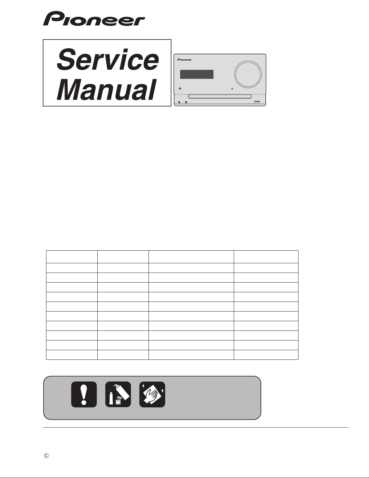
CD RECEIVER SYSTEM
PHONES AUDIO IN iPad
X-CM31-K
VOLUMETIMER
ORDER NO.
RRV4350
X-CM31-K
X-CM31-W,-R ,-T
X-CM31-K
,-W
/CXE
X-CM31DAB-K,-W,-R,-T
THIS MANUAL IS APPLICABLE TO THE FOLLOWING MODEL(S) AND TYPE(S).
Model Type Power Requirement Remarks
X-CM31-K SYXE8 AC 220 V to 240 V
X-CM31-W SYXE8 AC 220 V to 240 V
X-CM31-R SYXE8 AC 220 V to 240 V
X-CM31-T SYXE8 AC 220 V to 240 V
X-CM31-K CXE AC 120 V
X-CM31-W CXE AC 120V
X-CM31DAB-K VXE8 AC 220 V to 240 V
X-CM31DAB-W VXE8 AC 220 V to 240 V
X-CM31DAB-R VXE8 AC 220 V to 240 V
X-CM31DAB-T VXE8 AC 220 V to 240 V
/SYXE8
/SYXE8
/VXE8
PIONEER CORPORATION 1-1, Shin-ogura, Saiwai-ku, Kawasaki-shi, Kanagawa 212-0031, Japan
PIONEER ELECTRONICS (USA) INC. P.O. Box 1760, Long Beach, CA 90801-1760, U.S.A.
PIONEER EUROPE NV Haven 1087, Keetberglaan 1, 9120 Melsele, Belgium
PIONEER ELECTRONICS ASIACENTRE PTE. LTD. 253 Alexandra Road, #04-01, Singapore 159936
PIONEER CORPORATION
2012
K-FZV AUG.
2012 Printed in Japan
1
2 3 4
SAFETY INFORMATION
A
This service manual is intended for qualified service technicians; it is not meant for the casual do-it-
yourselfer. Qualified technicians have the necessary test equipment and tools, and have been trained
to properly and safely repair complex products such as those covered by this manual.
Improperly performed repairs can adversely affect the safety and reliability of the product and may
void the warranty. If you are not qualified to perform the repair of this product properly and safely, you
should not risk trying to do so and refer the repair to a qualified service technician.
WARNING
This product may contain a chemical known to the State of California to cause cancer, or birth defects or other reproductive
harm.
B
CAUTION
Health & Safety Code Section 25249.6 - Proposition 65
C
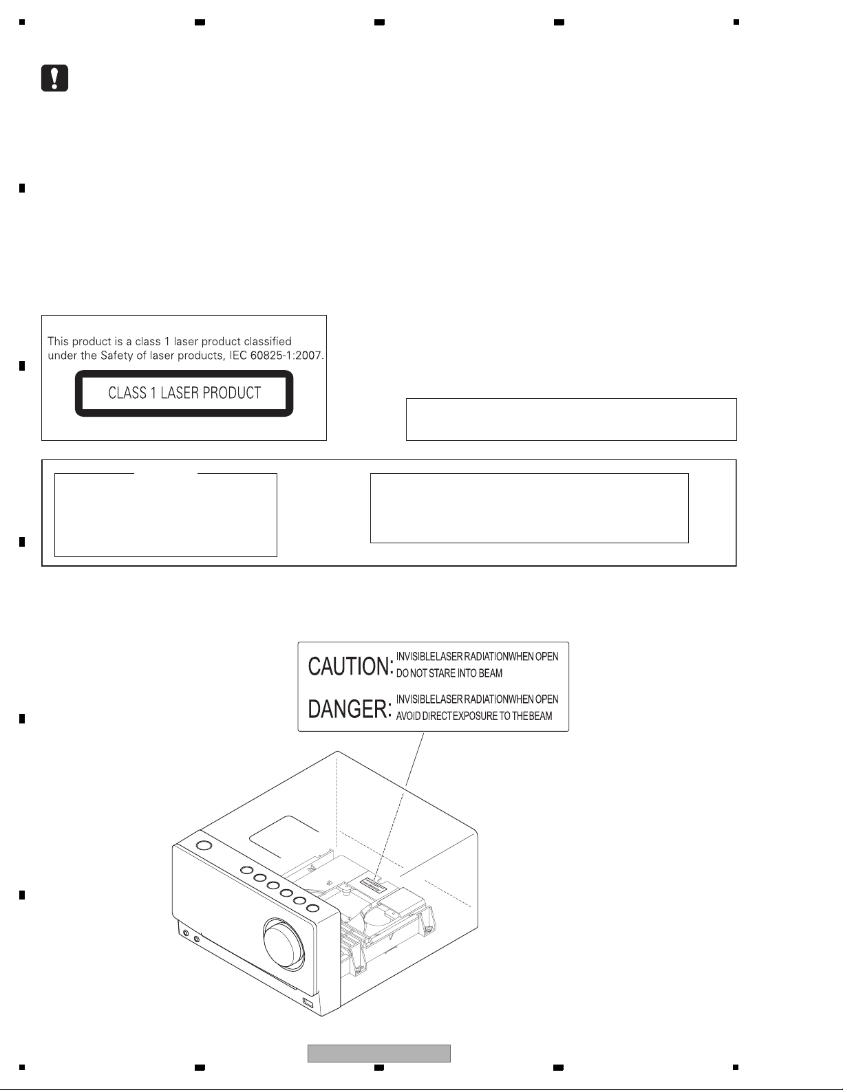
THIS PIONEER APPARATUS CONTAINS
LASER OF CLASS 1.
SERVICING OPERATION OF THE APPARATUS
SHOULD BE DONE BY A SPECIALLY
INSTRUCTED PERSON.
LABEL CHECK
D
IMPORTANT
D58-5-2-2a_A1_En
The following caution appears on your unit.
Location: inside of the unit
The laser component is capable of emitting radiation exceeding the limit for CLASS 1.
WARNING !
Aspecially instructed person should do servicing operation of the apparatus.
Laser Pickup specifications and Laser characteristics
For CD Wave length (typ) : 790 nm
Operation output : 5 mW CW, Class 1
Maximum output : Class 1 (Under fault condition)
E
F
2
1
2 3 4
X-CM31-K

5
6 7 8
CONTENTS
SAFETY INFORMATION..........................................................................................................................................................2
1. SERVICE PRECAUTIONS .................................................................................................................................................... 4
1.1 NOTES ON SOLDERING ...............................................................................................................................................4
2. SPECIFICATIONS................................................................................................................................................................. 5
2.1 ACCESSORIES ..............................................................................................................................................................5
2.2 SPECIFICATIONS ..........................................................................................................................................................5
3. BASIC ITEMS FOR SERVICE ..............................................................................................................................................6
3.1 CHECK POINTS AFTER SERVICING ........................................................................................................................... 6
3.2 PCB LOCATIONS ........................................................................................................................................................... 7
3.3 JIGS LIST ....................................................................................................................................................................... 7
4. BLOCK DIAGRAM ................................................................................................................................................................ 8
4.1 OVERALL CONNECTION DIAGRAM............................................................................................................................. 8
4.2 BLOCK DIAGRAM........................................................................................................................................................ 10
5. DIAGNOSIS ........................................................................................................................................................................12
5.1 TROUBLESHOOTING..................................................................................................................................................12
5.2 HOW TO EVALUATE LD DETERIORATION OF PICKUP ASSY..................................................................................14
6. SERVICE MODE ................................................................................................................................................................. 15
6.1 CONFIRM SOFTWARE VERSION AND DESTINATION INFORMATION.................................................................... 15
6.2 HOW TO CHANGE THE DESTINATION......................................................................................................................15
6.3 HOW TO CHANGE THE AM STEP.............................................................................................................................. 16
7. DISASSEMBLY ................................................................................................................................................................... 17
. EACH SETTING AND ADJUSTMENT ................................................................................................................................25
8
8.1 NECESSARY ADJUSTMENT POINTS ........................................................................................................................ 25
8.2 HOW TO UPDATE SOFTWARE................................................................................................................................... 25
9. EXPLODED VIEWS AND PARTS LIST...............................................................................................................................26
9.1 PACKING SECTION ..................................................................................................................................................... 26
9.2 EXTERIOR SECTION .................................................................................................................................................. 28
10. SCHEMATIC DIAGRAM .................................................................................................................................................... 32
10.1 SERVICE MAIN PCB (1/8) : MCU .............................................................................................................................. 32
10.2 SERVICE MAIN PCB (2/8) : IPOD CP CHIP..............................................................................................................34
10.3 SERVICE MAIN PCB (3/8) : FMDAB ..........................................................................................................................36
10.4 SERVICE MAIN PCB (4/8) : AMP............................................................................................................................... 38
10.5 SERVICE MAIN PCB (5/8) : MPEG............................................................................................................................40
10.6 SERVICE MAIN PCB (6/8) : ADC...............................................................................................................................42
10.7 SERVICE MAIN PCB (7/8) : POWER (1/2).................................................................................................................44
10.8 SERVICE MAIN PCB (8/8) : POWER (2/2).................................................................................................................46
10.9 SERVICE VFD+KEY PCB ..........................................................................................................................................48
10.10 SERVICE IPOD PCB................................................................................................................................................ 50
10.11 SERVICE USBPHONE PCB..................................................................................................................................... 52
11. PCB CONNECTION DIAGRAM........................................................................................................................................ 54
11.1 SERVICE MAIN PCB (Non DAB Model ).................................................................................................................... 54
11.2 SERVICE MAIN PCB (DAB Model ) ........................................................................................................................... 56
11.3 SERVICE VFD+KEY PCB ..........................................................................................................................................58
11.4 SERVICE IPOD PCB.................................................................................................................................................. 60
.5 SERVICE USBPHONE PCB....................................................................................................................................... 61
11
A
B
C
D
E
F
X-CM31-K
5
6 7 8
3

1
2 3 4
1. SERVICE PRECAUTIONS
1.1 NOTES ON SOLDERING
A
• For environmental protection, lead-free solder is used on the printed circuit boards mounted in this unit.
Be sure to use lead-free solder and a soldering iron that can meet specifications for use with lead-free solders for repairs
accompanied by reworking of soldering.
• Compared with conventional eutectic solders, lead-free solders have higher melting points, by approximately 40 ºC.
Therefore, for lead-free soldering, the tip temperature of a soldering iron must be set to around 373 ºC in general, although
the temperature depends on the heat capacity of the PC board on which reworking is required and the weight of the tip of
the soldering iron.
Do NOT use a soldering iron whose tip temperature cannot be controlled.
Compared with eutectic solders, lead-free solders have higher bond strengths but slower wetting times and higher melting
B
temperatures (hard to melt/easy to harden).
The following lead-free solders are available as service parts:
• Parts numbers of lead-free solder:
GYP1006 1.0 in dia.
GYP1007 0.6 in dia.
GYP1008 0.3 in dia.
C
D
E
F
4
1
2 3 4
X-CM31-K

5
6 7 8
2. SPECIFICATIONS
2.1 ACCESSORIES
Remote control unit X-CM31-K/SYXE8
X-CM31-R/SYXE8
X-CM31-T/SYXE8
X-CM31-W/SYXE8 :
X-CM31-K/CXE
X-CM31-W/CXE
X-CM31DAB-K/VXE8
X-CM31DAB-W/VXE8
X-CM31DAB-R/VXE8
X-CM31DAB-T/VXE8
AC Power cord SYXE8: VPE003202-0040
CXE: VPA004212-0040
VXE8: VPE00A213-0030
AM Loop antenna SYXE8: VTA100009-0010
CXE: VTA100009-0010
FM Wire antenna VTA400001-0020
Non-skid pads x 8 ASW503021-0045
iPad stand ASW200111-0001
Operating instructions SYXE8: YOM200145-0001
CXE: YOM200145-0004
VXE8: YOM200145-0002
AAA Dry cell battery x 2
Warranty card
A
WIR249004-AM01 (AXD7670)
WIR249004-AM02 (AXD7678)
WIR249004-AM05 (AXD7672)
WIR249004-AM06 (AXD7671)
B
C
2.2 SPECIFICATIONS
• Amplifier section
RMS Power Output: . . . . . . . . . . . . . . . . . . . . . . . . 15 W + 15 W
(1 kHz, 10 %, T.H.D., 8 Ω)
• Tuner section
Frequency Range (FM) . . . . . . . . . . . . . . 87.5 MHz to 108 MHz
Antenna Input (FM) . . . . . . . . . . . . . . . . . . . . 75 Ω unbalanced
Frequency Range (AM) . . . . . . . . . . . . . . 522 kHz to 1620 kHz
(Except DAB model)
Antenna (AM) . . . . . . . . . . . . . . . . . . . . . . . . . . . . Loop antenna
(Except DAB model)
•Miscellaneous
iPod/iPhone connector port . . . . . . . . . . . . . . . . . . . . . 5 V, 1 A
USB terminal . . . . . . . . . . . . . . . . . . . . . . . . . . . . . . . .5 V, 2.1 A
Power source . . . . . . . . . . . . . AC 220 V to 240 V, 50 Hz/60 Hz
Power consumption
Power on. . . . . . . . . . . . . . . . . . . . . . . . . . . . . . . . . . . . . 37 W
Power stand-by. . . . . . . . . . . . . . . . . . . . . . . . . . 0.5 W or less
Dimensions. . . . . . . 200 mm (W) x 123 mm (H) x 250.6 mm (D)
Weight (without package) . . . . . . . . . . . . . . . . . . . . . . . . 2.0 kg
• Speaker
Magnetically shieled speaker system
Type
2-way type speaker system
5 cm Tweeter
9.4 cm Woofer
Maximum input power . . . . . . . . . . . . . . . . . . . . . . . . . . . . 15 W
Impedance . . . . . . . . . . . . . . . . . . . . . . . . . . . . . . . . . . . . . . 8 Ω
Dimensions . . . . . . . 120 mm (W) x 200 mm (H) x 232.6 mm (D)
Weight . . . . . . . . . . . . . . . . . . . . . . . . . . . . . . . . . . . .2.0 kg/each
D
E
Note
• The specifications are applicable when the power supply
is 230 V.
• Specifications and the design are subject to possible
modifications without notice, due to improvements.
5
6 7 8
X-CM31-K
F
5
1
2 3 4
3. BASIC ITEMS FOR SERVICE
3.1 CHECK POINTS AFTER SERVICING
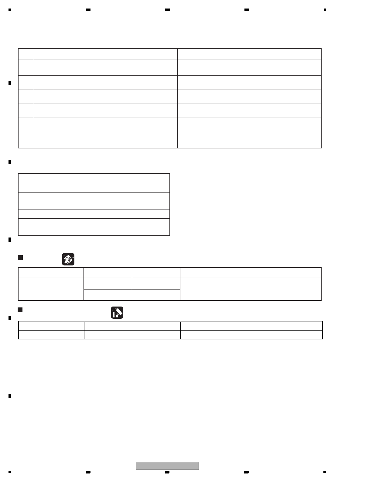
To keep the product quality after servicing, confirm recommended check points shown below.
A
No. Procedures Check points
Confirm whether the customer complain has been solved. The customer complain must not be reappeared.
1
Check the CD playback. Audio and operations (search, etc) must be normal.
2
Check the USB playback. Audio and operations must be normal.
3
Check the tuner operations. Audio and operations (Station Search, etc) must be normal.
4
Audio and operations must be normal.
B
Check the Line input playback. Audio and operations must be normal.
5
Check the appearance of the product. No scratches or dirt on its appearance after receiving it for
6
See the table below for the items to be checked regarding audio.
Item to be checked regarding audio
Distortion
Noise
C
Volume too low
Volume too high
Volume fluctuating
Sound interrupted
Cleaning
NamePosition to be cleaned Part No. Remarks
D
Cleaning liquidPickup lens GEM1004
Cleaning paper GED-008
service.
Lubricants and Glues List
Name Lubricants and Glues No. Remarks
Sillicone Bond GYA1001 Refer to "9.2 EXTERIOR SECTION"
E
F
6
1
2 3 4
X-CM31-K
5
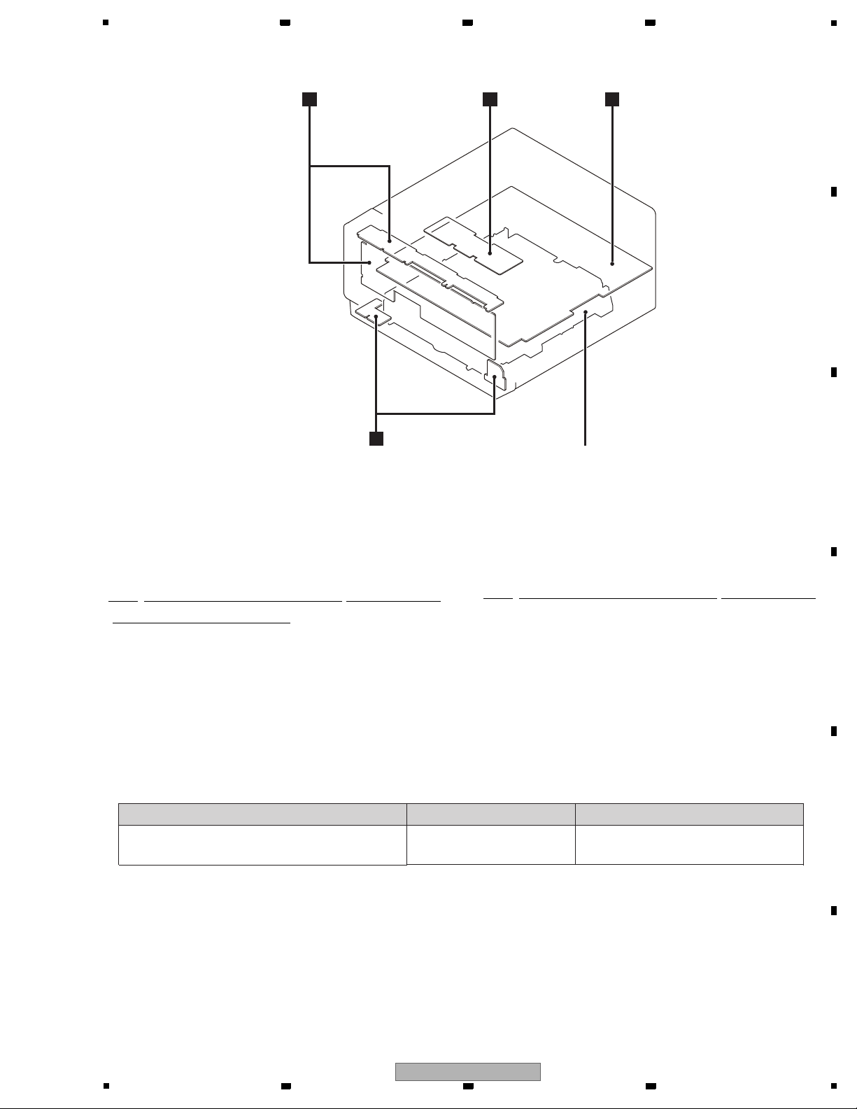
3.2 PCB LOCATIONS
6 7 8
SERVICE VFD+KEY PCB SERVICE IPOD PCB
B
D
SERVICE USBPHONE PCB Loader MechaLoader Mecha
SERVICE MAIN PCB
AC
Tr averse Mecha
A
B
C
NOTES: - Parts marked by “NSP” are generally unavailable because they are not in our Master Spare Parts List.
-
The > mark found on some component parts indicates the importance of the safety factor of the part.
Therefore, when replacing, be sure to use parts of identical designation.
Mark No. Description Part No.
LIST OF ASSEMBLIES
1..SERVICE MAIN PCB (SYXE8) APE205240-0001
1..SERVICE MAIN PCB (CXE) APE205240-0004
1..SERVICE MAIN PCB (VXE8) APE205240-0002
1..SERVICE VFD+KEY PCB APE205250-0001
Mark No. Description Part No.
1..SERVICE IPOD PCB APE205260-0001
1..SERVICE USBPHONE PCB APE205270-0001
1..Loader Mecha WMA200001-0001
1..Traverse Mecha WVD500002-0002
3.3 JIGS LIST
Name Jig No. Remarks
SP Connection cable
GGD1827
Corresponding to the Dedicated
SP Connector
D
E
F
X-CM31-K
5
6 7 8
7
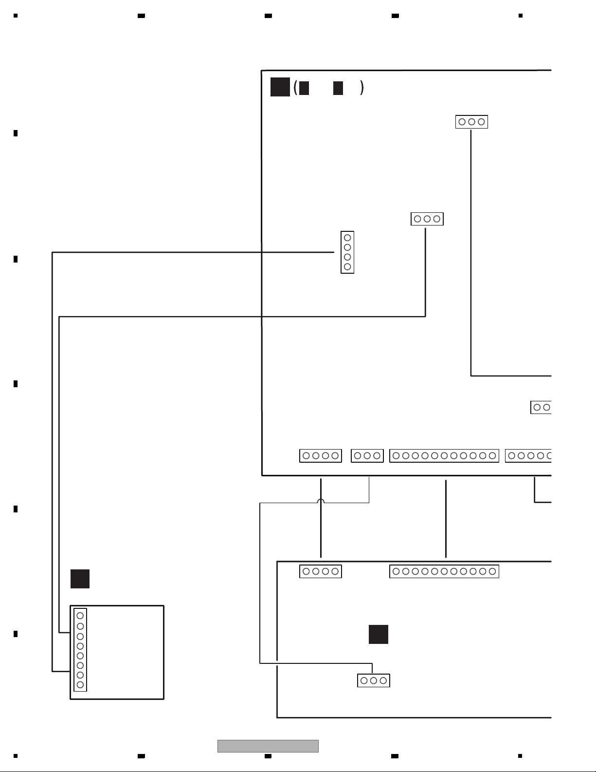
1
2
I
U
P
D
D
P
D
D
N
2 3 4
4. BLOCK DIAGRAM
4.1 OVERALL CONNECTION DIAGRAM
A
A
A 1/8 - A 8/8
To ipod video board
AUX_R_IN
GND
IPOD_VIDEO
3
21
VIDEO_GND
CN3
To Loader
To Loader
To lidar
SLE
SLE
LOA
LOA
TRAY_O
AG
TRAY_
GND
GND
CDMDI
PUH_CDLD
VR-CD
A_+5V
VREF1
GND
CD/DVD-SW
RADRAD+
FOC+
FOC-
S
S
NC
NC
NC
NC
E
F
B
A
RF
D
C
SERVICE MAIN PCB
(SYXE8 : APE205240-0001)
(CXE : APE205240-0004)
(VXE8 : APE205240-0002)
To AUX IN
B
GND
AUX_L_IN
21
3
CN20
HP_DET
123 4
HP_L
GND
HP_R
4P Line
3P AUX IN Line
to earphone board
C
CN19
To USB board
IPOD5V
IPOD5V
54
To panel power To panel key To panel display
CN6
To ipod board
-28V
CN412
-28V
3P KEY LIne
STB_KEY
3
21
CN21
B
3
21
STB_KEY
AD_KEY1
GND
AD_KEY1
12V
GND
D
+5V
123 4
CN901
panel power 4P Line
E
SERVICE USBPHONE PCB
D
(APE205270-0001)
8
NC
7
AUX_L_IN
GND
AUX _R IN
56
HP_DET
HR_L
GND
HR_R
123 4
F
CN18
123 4
12V
+5V
GND
To panel power
GND
VOLA_CTL
VOLB_CTL
TIMER_LED
10
11
9 8 76543
GND
STB_LED
IR_IN
MCU3.3V
CN1
VFD signal 11P Line
11
10
8 76543
9
GND
IR_IN
MCU3.3V
STB_LED
VOLA_CTL
VOLB_CTL
TIMER_LED
SERVICE VFD+KEY PCB
(APE205250-0001)
CN16
To panel key
DP_DO
DP_CLK
DP_DO
DP_CLK
DP_STB
21
21
DP_STB
GND
GND
6543
CN401
USB_D_
IPOD+5V
CN4
ACCESSOR
GND
USB_D+
8
1
2 3 4
X-CM31-K
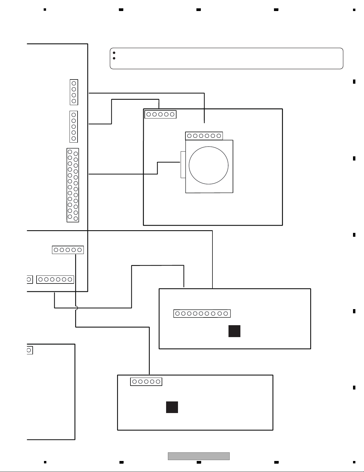
5
GND
GND
6 7 8
A
When ordering service parts, be sure to refer to "EXPLODED VIEWS and PARTS LIST" or "PCB PARTS LIST".
The > mark found on some component parts indicates the importance of the safety factor of the part.
Therefore, when replacing, be sure to use parts of identical designation.
CN3
To Loader
o Loader
TRAY_OUT
TRAY_IN
PUH_CDLD
To lidar
CD/DVD-SW
SB board
CN6
To ipod board
GND
USB_D+
1
USB_D_
6543
CN4
CN10
SP+
SP-
SLED+
SLED-
LOAD+
LOAD-
AGND
CN8
GND
GND
NC
NC
CDMDI
NC
VR-CD
NC
E
A_+5V
VREF1
GND
F
B
A
RF
D
C
RADRAD+
FOC+
FOC-
IPOD5V
IPOD5V
CD_USB_DM#
543 2
ACCESSOR
IPOD+5V
21
123 4
CN9
5
123 4
23
22 24
21
20
15 17 19
14 16 18
12
11 13
10
2468
1 3 579
CD_USB_DP#
AGND
1
IPOD_DET
5P Line
24P FFC Line
4P Line
4
LOAD-
TRAY_OUT
123
AGND
TRAY_IN
5
LOAD+
6P IPOD signal Line
SP+
SP-
6543 21
SLED+
3P IPOD Video Line
B
SLED-
C
Loader Mecha
D
1
CN401
Y PCB
)
CN6
7
IPOD_DET
ACCESSOR
VIDEO_GND
8
9
GND
C
IPOD_VIDEO
SERVICE IPOD PCB
(APE205260-0001)
E
CN6
5P USB line
CD_USB_DM#
AGND
CD_USB_DP#1IPOD5V
5432
IPOD5V
D-
D+
56
USB_POWER
123 4
GND
SERVICE USBPHONE PCB
D
(APE205270-0001)
F
X-CM31-K
5
6 7 8
9
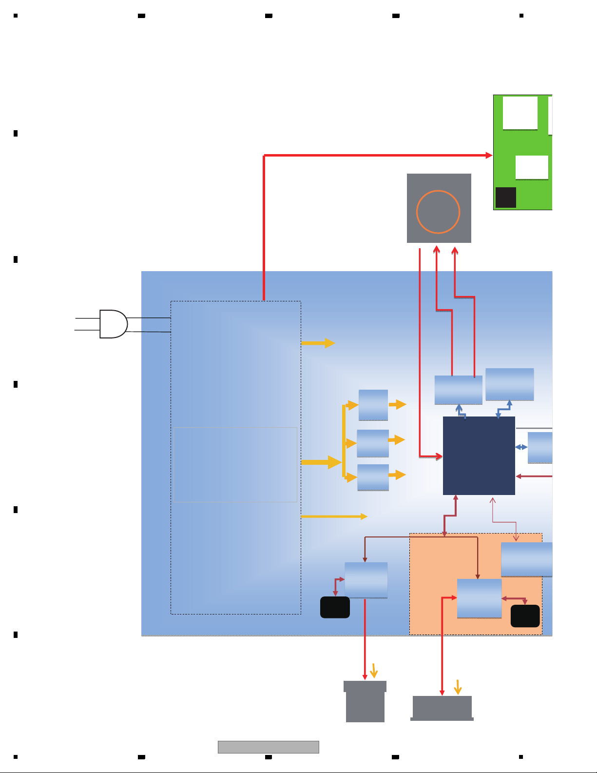
1
S
T
2
I
4.2 BLOCK DIAGRAM
A
2 3 4
IR
U402
VFD Power Line
POWER
LED
B
C
50/60HZ
SYXE8,VXE8 : AC220~240V
CXE : AC120V
D
Power Supply
AMP19V
SYS5V
LDO
(SGM2021)
U5
TPS2553
U3
AIC1519
U4
SYS3.3V
IPOD5V
USB5V
CD
LOAD
RF 24P Line
Motor driver
Line
tray
CD Deiver Line
(AM5888)
U15
Decoder
(SPHE8104GW)
U16
SERV
B
SDRAM
(EM638165TS-
6G)U18
MPEG_I
FLA
(EN25
U17
UART
MCU3.3V USB
I2C
IPOD CP
USB
R NET
(CHG)
USB sw
(SGM471)
U8
IPAD 5V
USB Line
2.1A
USB
Ipod Line
IPOD
USB sw
(SGM4717)
U6
IPOD 5V
1A
E
F
10
1
2 3 4
X-CM31-K
(FMI341S2500)
UA2
R NET
(CHG)
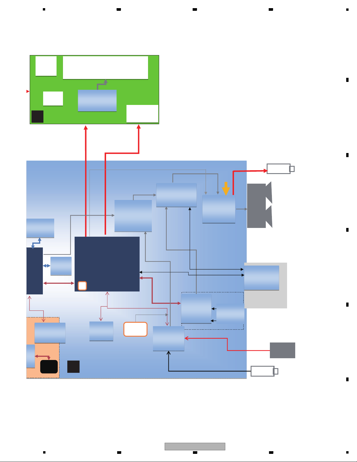
5
6 7 8
A
IR
U402
POWER
SERVICE VFD+KEY PCB
B
SDRAM
(EM638165TS-
6G)U18
LED
VFD
(8 charactors / 14 segments)
VFD Driver
(ET16311)
U401
VFD 11P Line
I2S
I2S Audio sw
(74VHC157 )
U12
KEYS
KEY Line
I2S Audio sw
(74VHC157 )
U13
19V
Audio AMP
(TAS5719)
U14
earphone
Line
15WX
2
(8R)
B
PH
C
er
4GW)
I2C
17)
MPEG_I2S
FLASH
(EN25T80)
U17
UART
IPOD CP
(FMI341S2500)
UA2
R NET
(CHG)
MCU
(PIC18F46J11)
U1
RTC
I2C
EEPROM
(24C02)
U2
SERVICE MAIN PCB
A
12.288MHz
U19
ADC _I2S
I2C
UART
MCLK
ADC _CLK
Audio ADC
(CS5346)
U20
DAB
Module
(Option)
U10
LINE_R/L
AUX_R/L
TU_I2S_DATA
I2S_CLK
I2C
FM /TUNER
4731
CN7
I2S
AM/FM
TUNER
CN7
TUNER
Module
Audio Line
AUX IN
AUX IN
D
E
Line IN
F
X-CM31-K
5
6 7 8
11
1
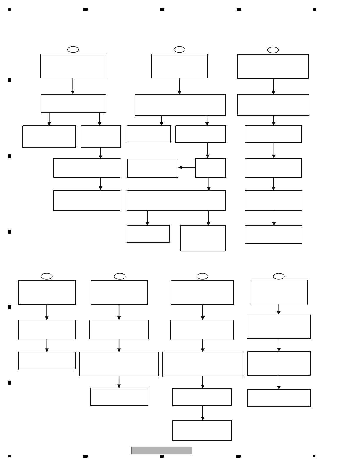
5. DIAGNOSIS
5.1 TROUBLESHOOTING
A
A
2 3 4
B
C
B
If connection is ok but
yet no working, need to
replace AC power code
C
All function not
working
Check AC power wire
connection all right
Check D911
STB5V and U1
3.3V all right
Check Q906 Q908 Q912
Q913 net all right for system
supply power
Change
SERVICE MAIN PCB
Yes
Yes
All SOURCE no
sound
Check remote whether it is mute or
VOL into minimum state, if ok, check
SPK connector all right
Press mute key or
adjust VOL
Check Q908 signal
line or change Q908
Check U1 pin 31
Check U14 pin19
line all right
Check U14 U13 and
AMP19V is all right
Not OK
Check U1 pin 31
line or update mcu
software
Yes
Check
Q908 5V
OK
Audio IN and line IN
both no sound
Check U20 pin 5/36/46
supply 3V3, pin14 supply
5V power
Yes
Check U20 pin 6 signal
line all right
Yes
Check U20 pin 1/2 line
all right
Yes
Check U20
pin 41/42/43/44 line
all right
Yes
Check U12 pin 1/16 line
all right
D
Line IN no
Check input jack
connector and source
signal all right
E
Check U20 pin 9/10
signal line all right
F
DE F
sound
Yes
Audio IN no
sound
Check input jack
connector and source
signal all right
Yes
Check the signal line between
SERVICE USBPHONE PCB
connector and SERVICE MAIN PCB
all right
Yes
Check U20 pin 11/12
net all right
Headphone no
output
Check headphone jack and
inserted headphone all right
Yes
Check the signal line between
SERVICE USBPHONE PCB
connector and SERVICE MAIN PCB
all right
Yes
Check U14 pin 8 signal
line power supply 3V3
Yes
Check U14
pin 1/2/3/4/47/48 line
all right
Check the connection
between USB socket
connector and SERVICE
MAIN PCB all right
Check U8 pin1 signal line
5V VCC power supply,
check pin 2/3/9/10 signal
line all right
G
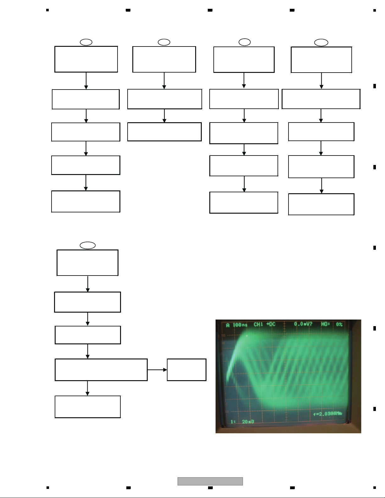
USB function
does not work
Yes
Yes
Check U16 pin 78 line for
USB power supply
12
X-CM31-K
1
2 3 4
5
6 7 8
H
Radio no sound
output (DAB)
Check U11 pin 1 output
VDD12 and pin 6 output
VDD18 is normal
Yes
Check U10 pin 30/35
RD33 is normal
Yes
Check U10
pin 7/8/22/25/28/29 signal
line all right
Yes
Defective IC, U10,
Change SERVICE MAIN PCB
I
Radio no sound
output
Check CN7 Tuner Module
solder and connection
all right
Yes
Defective Tuner Module
Change SERVICE MAIN PCB
J
Video no
output
Set TV OUT by remote
control unit to display
picture on TV
Yes
Check JK2 (video output)
connector and TV cable
all right
Yes
Check iPod socket solder
and video line all right
Yes
Change
SERVICE IPOD PCB
K
IPOD no play
Check the connection between
SERVICE IPOD PCB connector
and SERVICE MAIN PCB all right
Yes
Check U3 U4 U6 are
working all right
Yes
Check CN6 is all right,
important is USB
D+/D- and 5V VCC
Yes
Change
SERVICE MAIN PCB
A
B
C
L
CD no play
Check the connection
between Loader Mecha and
SERVICE MAIN PCB
Yes
Check Q1 Q7 Q8 are
working all right
Yes
Check CN8 pin 8 (RF waveform)
on the SERVICE MAIN PCB
*Refer to the RF waveform photograph.
OK
Change
SERVICE MAIN PCB
Not OK
Change
Traverse Mecha
D
RF waveform
E
F
X-CM31-K
5
6 7 8
13
1
2 3 4
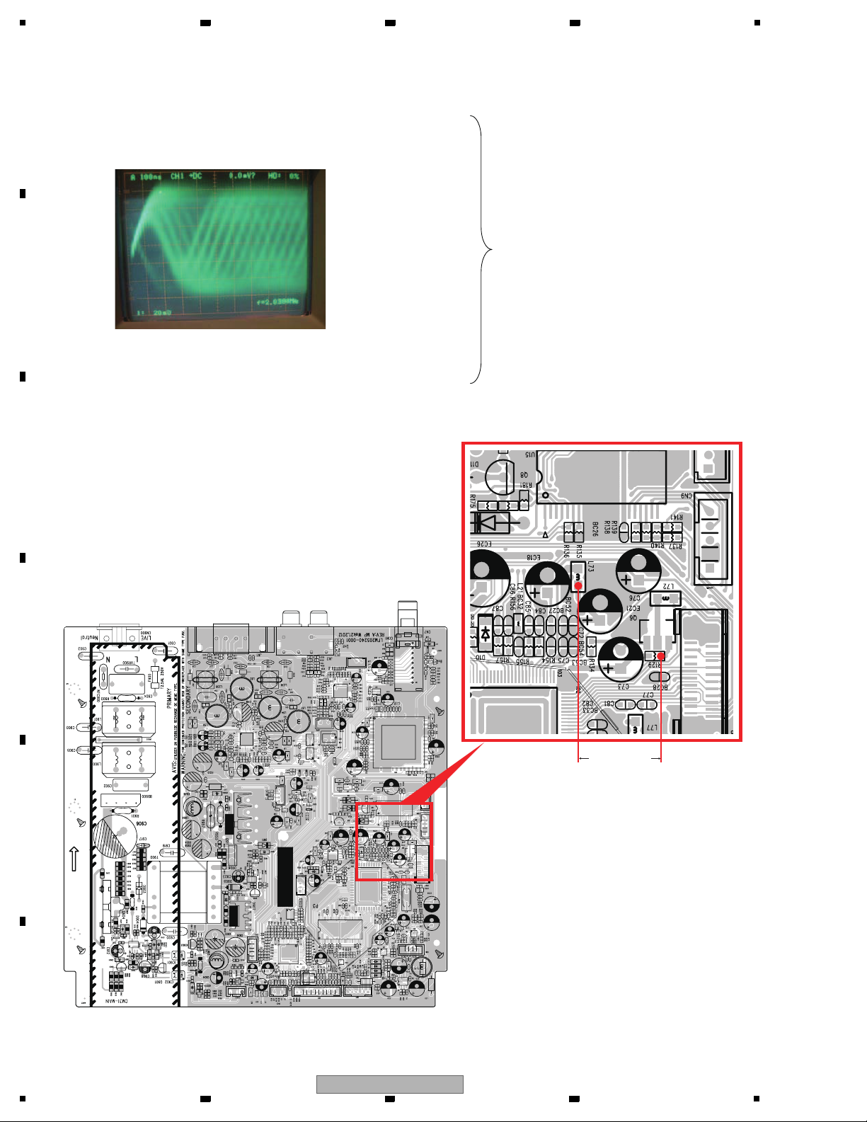
5.2 HOW TO EVALUATE LD DETERIORATION OF PICKUP ASSY
If CD cannot be played, LD of pickup ASSY may be deteriorated.
A
Carry out the evaluation in the following procedure.
Evaluate the waveform of CN8 8 pin (refer to the photo) of SERVICE MAIN PCB.
RF level : 1.0V(+/-0.25V)
If the value is 0.75V or less, 780-nm LD is deteriorated.
If LD is deteriorated based on the evaluation result,
replace Traverse Mecha with a new one.
B
Measure the voltage value between R129 and L73(3.3V) of SERVICE
MAIN PCB shown in the figure below.
If the value is 0.4V or more, 780-nm LD is deteriorated.
C
SERVICE MAIN PCB
D
DC voltage
measurement
E
F
14
1
2 3 4
X-CM31-K

5
6 7 8
6. SERVICE MODE
6.1 CONFIRM SOFTWARE VERSION AND DESTINATION INFORMATION
[Procedure]
1. Press STANDBY/ON key to turn on.
2. Press CD key to select CD function.
3. Press OPEN/CLOSE key to open disc tray.
4. Press STOP key.
5. Press 1 key.
6. Press 2 key.
7. Press 3 key.
8. Software version and destination information appear in main display.
9. If pressing any key, information disappears.
A
[The example of information]
E_C24M22 (Non DAB model)
*The first character indicates product destination.
E means Europe destination except for UK.
A means North America destination.
*C24M22 indicates software version.
C24 means software version of CD module, SPHE8104GW is C24.
M22 means software version of Main module, PIC18F46J11 is M22.
UKC25M35 (DAB Model)
*The first alphabet [UK] of two characters indicates product destination.
UK means United Kingdom destination.
*C25M35 indicates software version.
C25 means software version of CD module, SPHE8104GW is C25.
M35 means software version of Main module, PIC18F46J11 is M35.
6.2 HOW TO CHANGE THE DESTINATION
[Procedure]
1. Press STANDBY/ON key to turn on.
2. Press CD key to select CD function.
3. Press OPEN/CLOSE key to open disc tray.
4. Press STOP key.
5. Press 9.
6. Press 9.
7. Press 9.
8. [DEST CHG] blink in main display.
9. Select the destination by pressing LEFT or RIGHT key.
[DEST E] means Europe destination except for UK.
[DEST A] means North America destination.
10. Press ENTER key after selecting destination.
11. [WAITING] and [DEST OK] are displayed, then turn off automatically.
*If destination is changed, all settings return to default.
(X-CM31DAB : Can not change DESTINATION.)
B
C
D
E
F
X-CM31-K
5
6 7 8
15

1
2 3 4
6.3 HOW TO CHANGE THE AM STEP
[Procedure]
1. Insert AC cord.
A
2. Not power on status, press and hold STOP key on main unit.
3. AM frequency step is displayed in main display.
[AM 10KSP] means AM frequency is 10kHz step.
[AM 9KSP] means AM frequency is 9kHz step.
*If changing the AM step, all AM presets return to default.
(X-CM31DAB : Can not change AM frequency. X-CM31DAB has no AM Function.)
[Remarks]
The destination and AM Frequency Step settings are set to the appropriate settings for board
of each region before shipment.
It is setting needlessness fundamentally at the time of board exchange.
B
When there should be fault, setting change is possible in the above-mentioned procedure.
C
D
E
F
16
1
2 3 4
X-CM31-K
5
7. DISASSEMBLY
6 7 8
Note 1 : Do NOT look directly into the pickup lens. The laser beam may cause eye injury.
Note 2 : Even if the unit shown in the photos and illustrations in this manual may differ from your product, the procedures
described here are common.
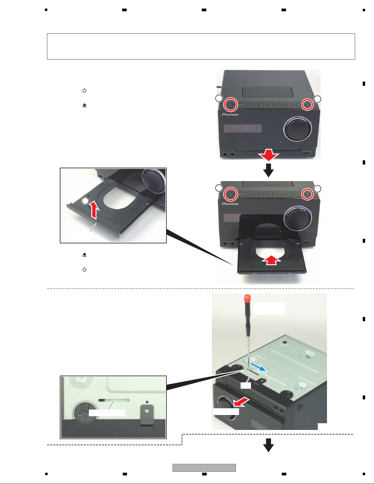
[1] Front Section
[1-1] Tray Door
(1) Press the STANDBY/ON button to turn on
the power.
(2) Press the OPEN/CLOSE button to open
the Tray.
(3) Remove upward the Tray Door.
1
5
2
4
3
A
B
C
Tray Door
(4) Press the OPEN/CLOSE button to close
the tray.
(5) Press the STANDBY/ON button to turn off
the power.
• How to open the Tray when the power
cannot be turned on
When the Tray cannot be opened because the
power cannot be turned on, open the Tray
forcibly in the method shown below.
Insert a Screwdriver (small) into the Slit located
at the bottom of the unit, and slide the Loading
Rack in the direction of blue arrow, as indicated
in the photo.
If the Tray pops out a little, fully pull it out by
hand.
Loading Rack
D
Screwdriver
(small)
E
Slit
Tray open
• Bottom view
F
X-CM31-K
5
6 7 8
17
1
2 3 4
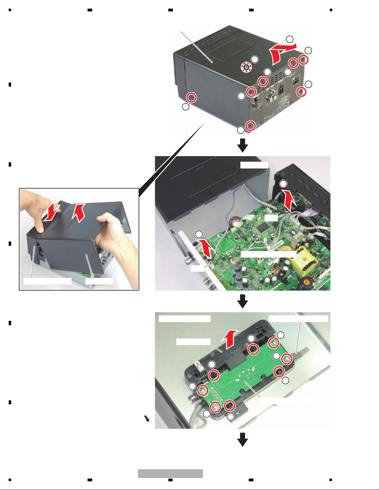
[1-2] Top Cover, SERVICE IPOD PCB
Remove the eight screws.
(1)
A
B
C
X-CM31-K/SYXE8 : HST053084-4060
X-CM31-R/SYXE8
X-CM31-T/SYXE8
X-CM31-K/CXE
X-CM31DAB-K/VXE8
(
X-CM31DAB-R/VXE8
X-CM31DAB-T/VXE8
X-CM31-W/SYXE8 : HST143084-1060
X-CM31-W/CXE
(
X-CM31DAB-W/VXE8
(2) Remove the Top Cover while lifting the rear
side of Top Cover.
Note :
*1: Remove them carefully because the SERVICE
IPOD PCB fixed on Top Cover side and the internal
parts of the product are connected with cable.
*2: If the engagement of the Top Cover with the
Hooks on Front Panel ASSY is too tight to
remove, press the central section of the Top
Cover from inside, then it becomes easy to
remove the Front Panel ASSY.
Hold
Press from inside
)
)
To p Co ve r
2
1
1
1
1
1
1
To p Co ve r
1
1
3
D
(3) Disconnect the two connectors and then
remove the Top Cover.
Note :
If diagnosis is not performed, the following steps
(4) through (7), are not required to be performed.
E
(4) Remove the screw (HSR050304-5080) and
then remove the Grounding Spring iPod.
(5) Remove the three screws.
(HSR050304-5080)
(6) Unhook the four Hooks and then remove the
iPod Bracket (with the SERVICE IPOD PCB).
Top CoverFront Panel ASSY
3
CN3
• Top Cover (inside)
iPod Bracket
5
CN4
SERVICE MAIN PCB
Grounding Spring iPod
6
6
5
4
6
SERVICE IPOD PCB
5
Front
F
18
1
2 3 4
X-CM31-K
6
5
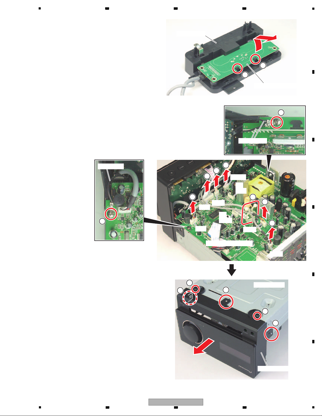
(7) Unhook the two Hooks and then remove the
SERVICE IPOD PCB.
[1-3] Front Section
(1) Release the two cables from the cord
clamper.
(2) Disconnect the six connectors.
(3) Remove the two screws (HST143084-1060)
and then remove the three GND cables.
6 7 8
iPod Bracket
7
7
SERVICE IPOD PCB
GND Cables
A
B
3
GND Cable
3
Notes on assembling
∗3: Nothing should be connected to the connector
:CN2, CN11. Please be careful not to connect
the cable by mistake.
(The CN11 connector is equipped only to the
initial lot. The connector :CN11 is not equipped
to the later lots.)
(4)
Remove the two screws.
X-CM31-K/SYXE8 : HST053084-4060
X-CM31-R/SYXE8
X-CM31-T/SYXE8
X-CM31-K/CXE
X-CM31DAB-K/VXE8
(
X-CM31DAB-R/VXE8
X-CM31DAB-T/VXE8
X-CM31-W/SYXE8 : HST143084-1060
X-CM31-W/CXE
(
X-CM31DAB-W/VXE8
(5) Unhook the three Hooks of the Front Panel
ASSY and then remove the Front Section.
)
)
2
2
2
2
CN21
CN1
CN6
SERVICE MAIN PCB
4
5
∗3
CN11
5
CN901
∗3
CN2
1
2
2
CN20
CN19
• Bottom view
4
5
Front Panel ASSY
C
D
E
F
X-CM31-K
5
6 7 8
19
 Loading...