

Page 1
^
)
DISPLAY ON/OFF TRACK NO. DIGITAL REC LEVEL
STANDBY/ON
+–
ORDER NO.
RRV2243
COMPACT DISC RECORDER
PDR-L77
THIS MANUAL IS APPLICABLE TO THE FOLLOWING MODEL(S) AND TYPE(S).
Type
KUXJ/CA AC120V
MYXJ AC220-230V
NVXJ AC230V
¶
This product is a system(s) component.
Be sure to connect it to the prescribed system component(s), otherwise damage may result.
Model
PDR-L77
tnenopmoCledoM
REVIECERDCOERETS77L-CX7322VRR7812VRR
METSYSREKAEPS
KCEDETTESSACOERETS77L-TC—————9912VRR
REDROCERCSIDINIM77L-JM—————1022VRR
REDROCERCSIDTCAPMOC77L-RDP3422VRR.launamsihT
————WRL-A-9L-S————
————————WRL-8L-S—————8712VRR
Power Requirement Remarks
WRL-9L-S————————
ledom.S.U
9322VRR6712VRR
launamecivreS
naeporuE
ledom
skrameR
This service manual should be used together with the following manual (s).
Model No. Order No. Remarks
PDR-509 RRV2055 Service guide
CONTENTS
1. SAFETY INFORMATION
2. EXPLODED VIEWS AND PARTS LIST
3. BLOCK DIAGRAM AND SCHEMATIC DIAGRAM
4. PCB CONNECTION DIAGRAM
5. PCB PARTS LIST
6. ADJUSTMENT
7. GENERAL INFORMATION
7.1 DIAGNOSIS
PIONEER CORPORATION 4-1, Meguro 1-chome, Meguro-ku, Tokyo 153-8654, Japan
PIONEER ELECTRONICS SERVICE, INC. P.O. Box 1760, Long Beach, CA 90801-1760, U.S.A.
PIONEER ELECTRONIC (EUROPE) N.V. Haven 1087, Keetberglaan 1, 9120 Melsele, Belgium
PIONEER ELECTRONICS ASIACENTRE PTE. LTD. 253 Alexandra Road, #04-01, Singapore 159936
c
PIONEER CORPORATION 1999
...............................................
....................................................
..................................................
......................................
...............
...
.........................
................................
2
5
10
35
46
51
57
57
FOR U.S. MODELS
NECESSARY INFORMATION FOR DHHS RULES
MARKED ON THE REAR BASE AND ON THE TOP
OF CD MECHANISM AS BELOW.
DANGER – LASER RADIATION WHEN OPEN.
AVOID DIRECT EXPOSURE TO BEAM.
7.1.1 POWER ON SEQUENCE
7.1.2 ERROR CODE
7.1.3 DISASSEMBLY
7.2 PARTS
7.1.2 IC
7.1.2 DISPLAY
8. PANEL FACILITIES AND SPECIFICATIONS
..........................................................
............................................................
.................................................
......................
.......................................
......................................
T – ZZE NOV. 1999 Printed in Japan
.......
57
59
61
63
63
68
70
Page 2
PDR-L77
1. SAFETY INFORMATION
This service manual is intended for qualified service technicians ; it is not meant for the casual do-ityourselfer. Qualified technicians have the necessary test equipment and tools, and have been trained
to properly and safely repair complex products such as those covered by this manual.
Improperly performed repairs can adversely affect the safety and reliability of the product and may
void the warranty. If you are not qualified to perform the repair of this product properly and safely, you
should not risk trying to do so and refer the repair to a qualified service technician.
WARNING
This product contains lead in solder and certain electrical parts contain chemicals which are known to the state of California to cause
cancer, birth defects or other reproductive harm.
Health & Safety Code Section 25249.6 – Proposition 65
NOTICE
(FOR CANADIAN MODEL ONLY)
Fuse symbols (fast operating fuse) and/or (slow operating fuse) on PCB indicate that replacement parts must
be of identical designation.
REMARQUE
(POUR MODÈLE CANADIEN SEULEMENT)
Les symboles de fusible (fusible de type rapide) et/ou (fusible de type lent) sur CCI indiquent que les pièces
de remplacement doivent avoir la même désignation.
(FOR USA MODEL ONLY)
1. SAFETY PRECAUTIONS
The following check should be performed for the
continued protection of the customer and service
technician.
LEAKAGE CURRENT CHECK
Measure leakage current to a known earth ground (water
pipe, conduit, etc.) by connecting a leakage current tester
such as Simpson Model 229-2 or equivalent between the
earth ground and all exposed metal parts of the appliance
(input/output terminals, screwheads, metal overlays, control
shaft, etc.). Plug the AC line cord of the appliance directly
into a 120V AC 60Hz outlet and turn the AC power switch
on. Any current measured must not exceed 0.5mA.
Reading should
not be above
0.5mA
Earth
ground
Device
under
test
Also test with
plug reversed
(Using AC adapter
plug as required)
Leakage
current
tester
Test all
exposed metal
surfaces
ANY MEASUREMENTS NOT WITHIN THE LIMITS
OUTLINED ABOVE ARE INDICATIVE OF A POTENTIAL
SHOCK HAZARD AND MUST BE CORRECTED BEFORE
RETURNING THE APPLIANCE TO THE CUSTOMER.
2. PRODUCT SAFETY NOTICE
Many electrical and mechanical parts in the appliance
have special safety related characteristics. These are
often not evident from visual inspection nor the protection
afforded by them necessarily can be obtained by using
replacement components rated for voltage, wattage, etc.
Replacement parts which have these special safety
characteristics are identified in this Service Manual.
Electrical components having such features are identified
by marking with a
in this Service Manual.
The use of a substitute replacement component which does
not have the same safety characteristics as the PIONEER
recommended replacement one, shown in the parts list in
this Service Manual, may create shock, fire, or other hazards.
Product Safety is continuously under review and new
instructions are issued from time to time. For the latest
information, always consult the current PIONEER Service
Manual. A subscription to, or additional copies of, PIONEER
Service Manual may be obtained at a nominal charge from
PIONEER.
on the schematics and on the parts list
AC Leakage Test
2
Page 3
PDR-L77
LABEL CHECK
THIS PIONEER APPARATUS CONTAINS
IMPORTANT
LASER OF CLASS ΙΙΙ b.
SERVICING OPERATION OF THE APPARATUS
SHOULD BE DONE BY A SPECIALLY
INSTRUTED PERSON.
NVXJ type
Put on Top Plate
LASER DIODE CHARACTERISTICS
MAXIMUM OUTPUT POWER: 23 mW
WAVELENGTH: 778 – 787 nm
MYXJ type
USYNLIG LASERSTRÅLING VED ÅBNING NÅR SIKKERHED SAFBRYDERE ER UDE AF FUNKTION.
UNDGÅ UDSÆTTELSE FOR STRÅLING
UNSICHTBARE LASER-STRAHLUNG TRITT AUS, WENN DECKEL
(ODER KLAPPE) GEÖFFNET IST! NICHT DEM STRAHL AUSSETZEN!
Put on Top Plate
MYXJ type
ADVARSEL
VORSICHT!
VRW1094
Put on Top Plate
MYXJ and NVXJ types
Put on Bottom Base
KUXJ/CA Type
Put on Bridge
Additional Laser Caution
1. Laser Interlock Mechanism
The position of the switch (S601) on the SERVO
MECHANISM Assy for detecting loading state is detected
by the system microprocessor, and the design prevents
laser diode oscillation when the switch (S601) is not on
CLMP terminal side (CLMP signal is OFF or high level.).
Thus, the interlock will no longer function if the switch
(S601) is deliberately set to CLMP terminal side (low
level).
The interlock also does not function in the test mode ∗.
Laser diode oscillation will continue, if pin 1 of M51593FP
(IC101) on the PRE-AMP BOARD ASSY mounted on the
CD-R PICKUP is connected to GND, or pin 19 is
connected to low level (ON), or else the terminals of Q101
are shorted to each other (fault condition).
2. When the cover is opened with the servo mechanism
block removed and turned over, close viewing of the
objective lens with the naked eye will cause exposure to a
Class 1 laser beam.
∗ Refer to page 51.
3
Page 4
PDR-L77
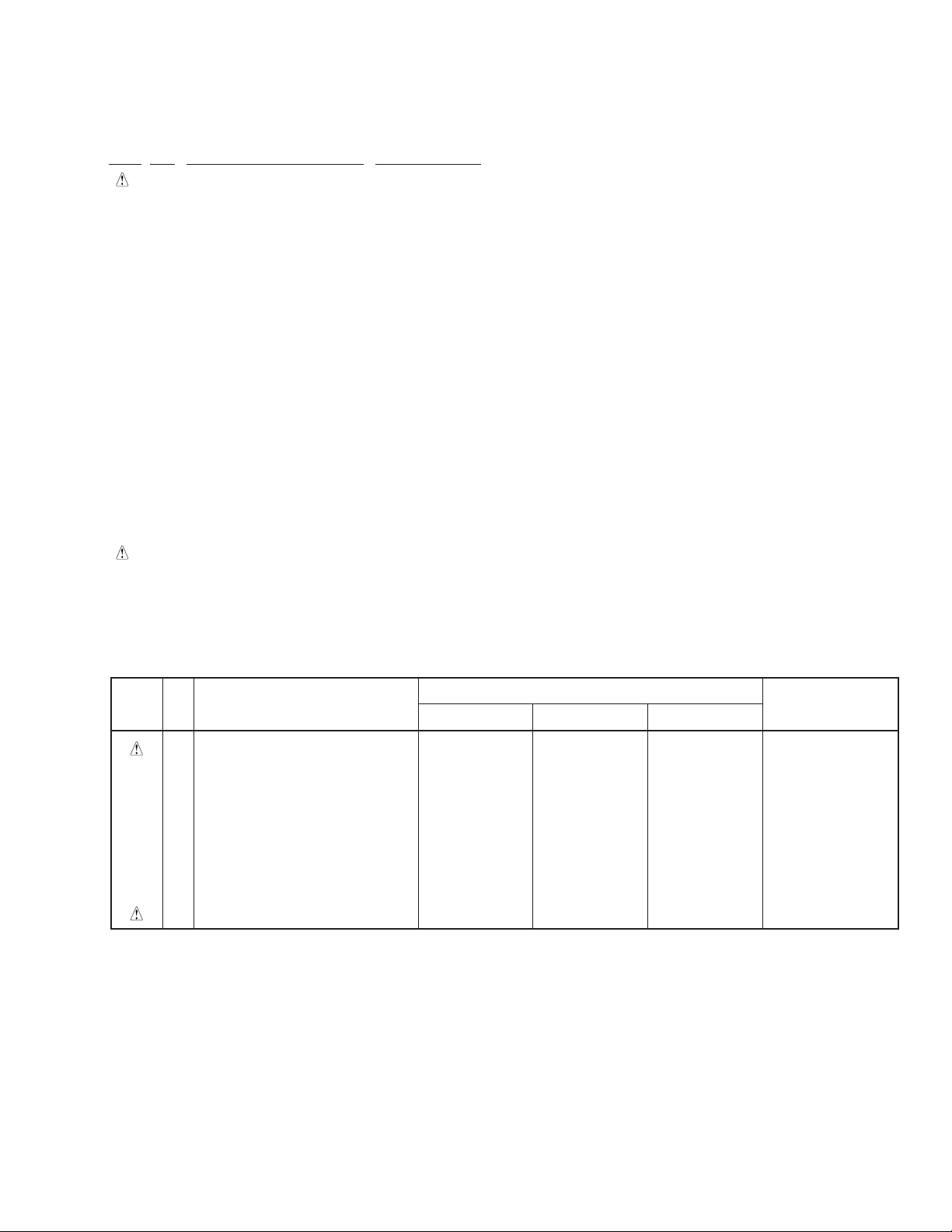
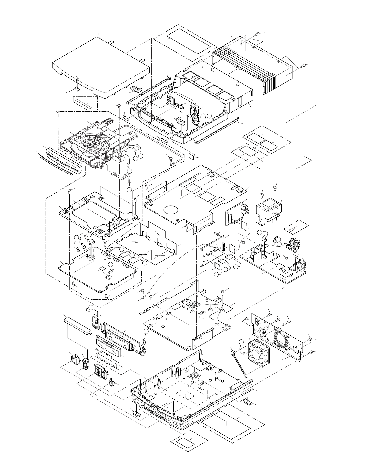
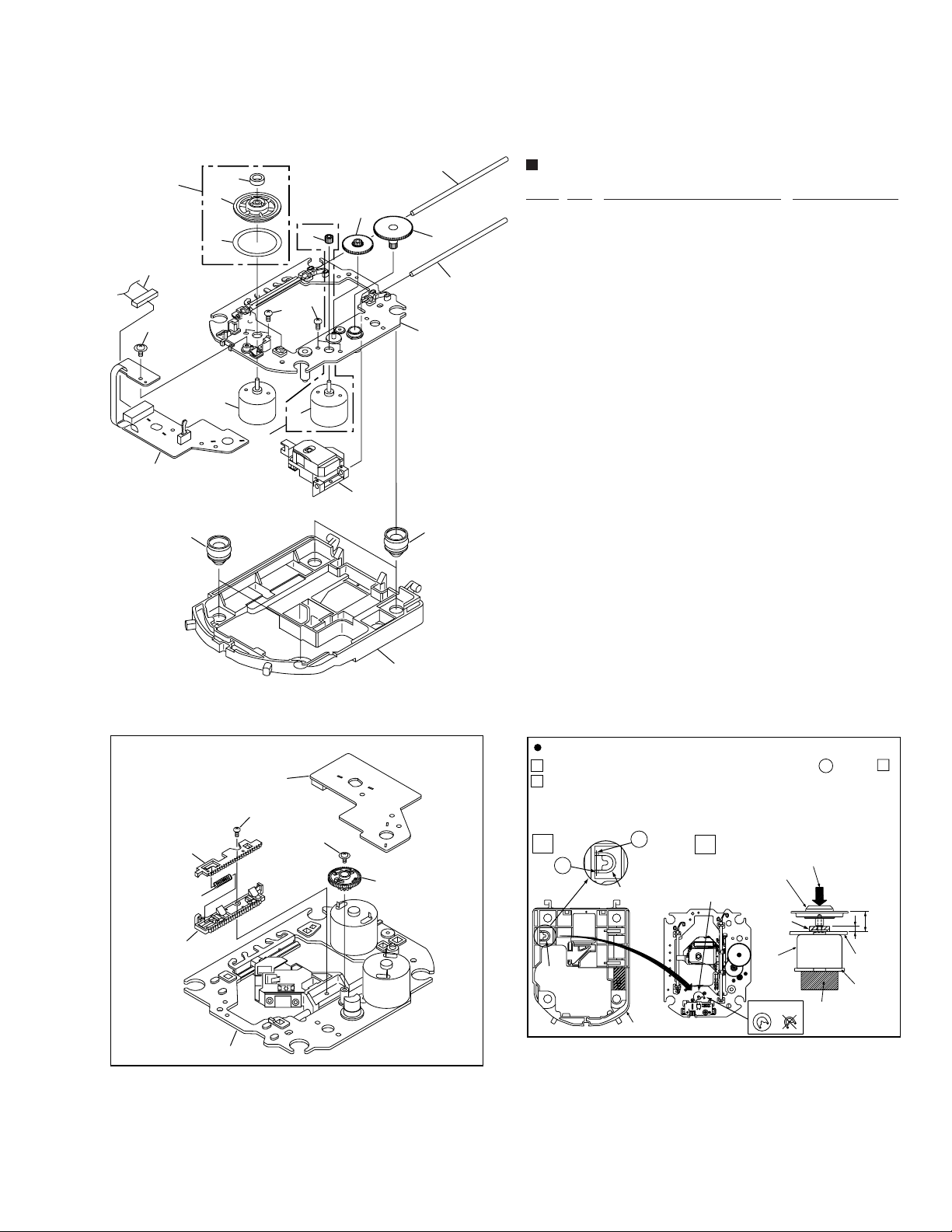
2. EXPLODED VIEWS AND PARTS LIST
NOTES : Parts marked by “ NSP ” are generally unavailable because they are not in our Master Spare Parts List.
The mark found on some component parts indicates the importance of the safety factor of the part.
Therefore, when replacing, be sure to use parts of identical designation.
Screw adjacent to mark on the product are used for disassembly.
2.1 PACKING
10
9
1
NVXJ type
only
20
12
18
PDR-L77
Except NVXJ type
1
5
6
7
8
16
15
KUXJ/CA and NVXJ types
MYXJ type
MYXJ type
4
only
only
only
14
11
13
2
3
4
17
19
Page 5
(1) PACKING PARTS LIST
Mark No. Description Part No.
1 AC Power Cord
2 Operating Instructions
3 Operating Instructions
4 Operating Instructions
NSP 5 Warranty Card
6 Remote Control Unit AXD7242
(CU-PD113)
7 Battery Cover RZN1156
8 Analog Recording Adapter AXY7000
9 Stereo Audio Cord PDE1126
10 Control Cord(Mini-plug Cord) ADE7056
11 Optical Cord RKX1031
NSP 12 Dry Cell Battery(R6P, AA) VEM-013
13 Polyethylene Bag Z21-038
(0.03×230×340)
14 P Pad F AHA7285
15 P Pad R AHA7286
16 Sub Packing AHD7842
17 Packing Case
18 Packing Sheet AHG7065
19 Spacer AHD7856
20 Fuse (T5A)
See Contrast table (2)
See Contrast table (2)
See Contrast table (2)
See Contrast table (2)
See Contrast table (2)
See Contrast table (2)
See Contrast table (2)
PDR-L77
(2) CONTRAST TABLE
PDR-L77/KUXJ/CA, MYXJ and NVXJ are constructed the same except for the following:
No.
Symbol and Description
KUXJ/CA type MYXJ type NVXJ type
1 AC Power Cord ADG7022 ADG1154 ADG1156
2 Operating Instructions ARE7251 Not used ARE7251
(English/French)
3 Operating Instructions Not used ARC7288 Not used
(Swedish/Dutch/Portuguese/Spanish)
4 Operating Instructions Not used ARE7250 Not used
(English/French/Italian/German)
NSP 5 Warranty Card ARY7023 ARY7022 ARY7022
17 Packing Case AHD7844 AHD7841 AHD7843
20 Fuse (T5A) Not used Not used AEK7001
Part No.
RemarksMark
5
Page 6
PDR-L77
2.2 EXTERIOR
28
KUXJ/CA type only
15
Refer to
"2.3 CD-R CORE ASSY (1/2)",
"2.4 CD-R CORE ASSY (2/2)".
24
26
45
50
41
37-1
52
27
34
KUXJ/CA type only
32
42
25
3
35
27
H
I
G
J
45
52
45
A
25
43
47
37-2
54
KUXJ/CA type: 39
NVXJ type: 57
19
45
4
47
MYXJ type only
56
45
10
53
31
36
I
J
52
22(1/2)
KUXJ/CA type
45
H
B
49
48
G
52
22(2/2)
29
F
C
D
45
12
2
23
30
44
A
17
48
1
45
6
9
D
C
7
B
44
20
E
21
47
11
F
33
E
45
5
47
47
46
18
38
only
14
47
47
16
55
MYXJ and NVXJ types only
16
40
KUXJ/CA type only
6
Page 7
(1) EXTERIOR PARTS LIST
PDR-L77
Mark No. Description Part No.
NSP 1 CDR ASSY AWM7486
2 FLDP ASSY AWU7522
3 FRKB ASSY AWU7523
4 PJB ASSY AWU7524
5 PWSB ASSY
6 21P FFC/30V ADD7207
7 15P FFC/30V ADD7208
8 25P FFC/60V ADD7209
9 16P FFC/60V ADD7210
10 Power Transformer
11 DC Fan Motor AXM7014
NSP 12 Cord With Plug (J1) DE015WC0
13 Connector Assy PG06KK-F15
14 Fuse (FU101)
NSP 15 CD-R CORE Assy PXA1625
16 Leg AEB7197
17 Mecha Barrier AEC7246
18 Rear Panel
NSP 19 Top Plate ANF7014
NSP 20 Bottom Plate ANF7019
21 Fan Plate ANG7153
22 Level Button AAD7569
23 Display Window AAK7717
24 Tray Panel AAN7197
25 Main Line AAP7058
See Contrast table (2)
See Contrast table (2)
See Contrast table (2)
See Contrast table (2)
Mark No. Description Part No.
31 PCB Cover AEC7247
32 Bonnet AMA7012
33 Bottom Base AMA7016
34 Button Assy A AWL7044
35 Button Assy B AWL7045
36 Power Button Assy AWL7049
37 Top Panel Assy AWL7053
NSP 37-1 Top Panel 1 AMB7682
NSP 37-2 Top Panel 2 AMB7683
38 Fuse Label
39 65 Label
40 Name Label
NSP 41 Caution Label
42 Disc Caution Label
43 CDR Getter Label PRW1547
44 Screw BBT30P060FZK
45 Screw BBZ30P060FMC
46 Screw BBZ30P300FZK
47 Screw VPZ30P080FZK
NSP 48 PCB Spacer AEC1371
49 Radiation Seat PEB1306
NSP 50 Mecha Base PNB1613
51 • • • • • • • •
52 Screw BBZ30P080FCC
53 CD-R CORE PCB ASS'Y PYY1273
See Contrast table (2)
See Contrast table (2)
See Contrast table (2)
See Contrast table (2)
See Contrast table (2)
26 Tray Line AAP7059
27 Front Line AAP7067
28 CL Lens AAX7704
29 R.C Lens AAX7772
30 FL Filter AEC7235
54 Caution Label
55 Label
56 Caution Label
57 Caution Label
(2) CONTRAST TABLE
PDR-L77/KUXJ/CA, MYXJ and NVXJ are constructed the same except for the following:
No.
Symbol and Description
KUXJ/CA type MYXJ type NVXJ type
5 PWSB ASSY AWU7537 AWU7521 AWU7521
10 Power Transformer ATT7066 ATT7065 ATT7065
14 Fuse (400mA : FU101) REK1125 Not used Not used
14 Fuse (T200mA : FU101) Not used REK1015 REK1015
18 Rear Panel ANC7905 ANC7902 ANC7904
38 Fuse Label AAX7781 Not used Not used
39 65 Label ARW7050 Not used Not used
NSP 41 Caution Label PRW1516 Not used Not used
40 Name Label ARW7076 Not used Not used
42 Disc Caution Label ARW7087 Not used Not used
54 Caution Label Not used PRW1233 Not used
55 Label Not used VRW-328 VRW-328
56 Caution Label Not used VRW1094 Not used
57 Caution Label Not used Not used PRW1018
Part No.
See Contrast table (2)
See Contrast table (2)
See Contrast table (2)
See Contrast table (2)
RemarksMark
7
Page 8
PDR-L77
2.3 CD-R CORE ASSY (1/2)
• Bottom View
A
18
13
1
20
9
12
7
26
25
Refer to
"2.4 CD-R CORE ASSY (2/2)".
23
31
24
19
5
28
26
29
5
30
5
6
21
4
17
8
3
CD-R CORE ASSY (1/2) PARTS LIST
Mark No. Description Part No.
NSP 1 LOADING A Assy PWZ3760
NSP 2 LOADING B Assy PWZ3761
3 Connector Assy PG02KK-E15
(LOADING B CN551 ↔ LOADING A CN502)
4 DC Motor (LOADING) PXM1027
15
A
2
27
22
14
11
16
10
Mark No. Description Part No.
15 Drive Cam VNL1736
16 Lock Plate VNL1820
17 Tray Stopper VNL1739
18 Connector Assy PG03KK-E37
(LOADING A CN501 ↔ CD-R CORE CN451)
5 Screw VBA1065
6 Motor Pulley PNW1634
7 Screw VBA1055
8 Tray Stopper Spring VBH1277
9 Rubber Belt VEB1260
10 Loading Base VNL1854
11 Tray VNK4570
12 Gear Pulley VNL1733
13 Loading Gear VNL1734
14 Drive Gear VNL1735
8
19 Screw BBZ26P040FMC
20 Screw Z39-019
21 Loading Motor Assy VXX2505
NSP 22 Binder ZCA-T18S
23 Clamper Plate VNE2068
24 Bridge VNE2069
25 Clamper VNL1738
26 Screw IPZ26P060FMC
27 32P Flexible Cable / 30V PDD1195
(CD-R Pickup ↔ CD-R CORE CN101)
NSP 28 Earth Lead Unit PDF1200
29 Tray Holder PNM1346
30 Stopper DNH2076
31 Spacer PNM1334
Page 9
2.4 CD-R CORE ASSY (2/2)
PDR-L77
17
22
25
1
20
15
23
9
23
3
7
2
26
4
10
21
19
11
18
16
5
8
CD-R CORE ASSY (2/2) PARTS LIST
Mark No. Description Part No.
NSP 1 SERVO MECHANISM Assy PWZ3759
2 DC Motor Assy (SPINDLE) PEA1235
NSP 3 DC Motor (CARRIAGE) PXM1042
4 Float Rubber A AEB7063
5 Float Rubber B AEB7066
NSP 6 Rack Spring DBH1285
NSP 7 Reflection Sheet PNM1325
8 Servo Base PNW2853
9 Pinion Gear PNW2854
10 Gear A PNW2855
11 Gear B PNW2856
12 Gear C PNW2857
13 Rack PNW2858
14 Rack Stopper PNW2859
NSP 15 Disc Table PNW2860
16 Carriage Base S PNW2874
17 Connector Assy PG09KK-E17
(SERVO MECHANISM CN601↔ CD-R CORE CN452)
18 Guide Bar VLL1488
19 Sub Guide Bar VLL1489
NSP 20 Magnet VYM1024
21 CD-R Pickup PEA1351
22 Screw Z39-018
23 Screw PMZ20P030FMC
24 Screw JGZ17P030FMC
25 Disc Table Assy PEA1349
26 Carriage Motor Assy PEA1350
• Bottom View
SERVO MECHANISM
ASSY
14
13
Carriage Base S
How to Install the Disc Table
Use nippers or other tool to cut the two sections marked A in figure 1 .
1
While supporting the spindle motor shaft with the stopper, put spacer on
2
24
22
12
6
top of the carriage base, and stick the disc table on top (takes about 9kg
pressure). Take off the spacer.
1
A
Spacer
A
Spacer
Servo Base
2
Spacer setting
Position
Disc table Assy
(Pressure of about 9kg)
Spacer
Spindle
motor
OK NG
Stopper
2.8mm
Carriage
Base
PCB
11mm
9
Page 10
1
23
PDR-L77
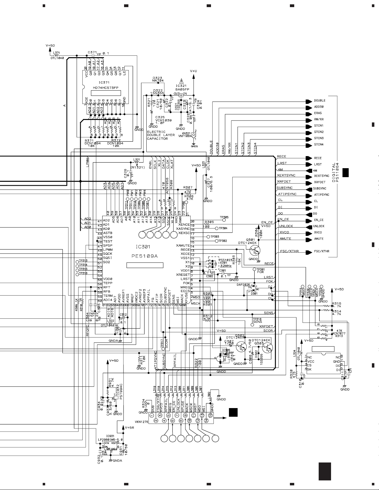
3. BLOCK DIAGRAM AND SCHEMATIC DIAGRAM
3.1 BLOCK DIAGRAM (1/2)
A
F
PJB ASSY
(PB)
(AI)
OPT OUT
OPT IN
B
JA7602
JA7601
(DI)
(DO)
(PB) (PB)
(AI) (AI)
CN7201 CN7704
23
LOUT
24
GNDA
13
LIN
24
GNDA
7
RECD
8
CDRD
2
FLAC1
12
VA+5
22
VA+5
3
(DI)
(DO)
CN7202
1
268759104111215161920
17
21
18
5
16
4
11
20
VD+5
DIN1
DOUT
GNDD
GNDD
VA-5
VFDP
POWER
VU+5
4
(PB)
3
2
13
12
19
18
24
14
4
23
9
5
8
21
10
22
15
6
GNDA1
GNDA2
VA+5A
VA+5D
(DI)
GNDD1
GNDD2
(AR)
(DO)
LINE OUT
LINE IN
JA7202
JA7201
(AI)
LIN
LOUT
GNDA
GNDA
20 1516 12
(PB)
RECD
CDRD
FLAC1
VA+5
VA+5
VD+5
VA-5
GNDD
VFDP
68759104111219
POWER
VU+5
CN7003
IC7006
JA7603
C
T7002
D7001
+
+
5V
IC7005
5V
KN7001
1
2
3
4
5
6
VA+5
GNDA
VA+5
GNDD
V+U
GNDU
1
2
3
4
5
6
CN7002 CN901
Q7007(-5V)
FU101
RY7001
T7001
Q7051
D7051
+
D7012
IC7052
5V
++
Q7008(VIDP)
Q7010
CN101
D
10
G
PWSB ASSY
CN7001
FAN
1234
Page 11
(AR)
(PB)
Q7241
E
5
PB AMP
IC7241
BA-4558F
VA-5
GNDA1
+
–
IC7101
BA-4558F
VA+5A
VA-5
GNDA2
CDR ASSY
POWER
51 41 65 61 76 77
SYSTEM µ-com
GNDD1
CN7702
1
VA+5A
+
–
ALC
REMOTE
CDRD
RECD
IC7501
PE5138A
2
678
(PB)
P ASSIVE
L.P .F .
16 20
D/A
IC7401
PCM1716E
7
GNDD1 GNDA1
IC7102
BA-4558F
VA+5A
(AR)
VA-5
VU+5
KEY1
KEY2
(REC)
GNDD2
CN7701
(PB)
19
VA+5D
(PB)
2
19
VA+5D
123
A/D
IC7301
PCM1800
17
24
15
(PB)
GNDA2GNDD1
GNDD2
(DO)
(DI)
3
1
4
9
5
GNDD1
141621
16
REMOTE
VU+5
15
KEY2
14
KEY1
6
GNDD
5
VFDP
4
3
VD+5
2
FLAC1
CN7502
CN7501
J7501
KEY
1
2
3
11
12
13
14
15
CN7502
H
I
FRKB ASSY
3
GNDD
3
49
FL DRIVER
48
IC7551
57
MSM9202
FL TUBE
V7001
FLDB ASSY
PDR-L77
4
KEY2
4
REMOTE
RECEIVER
UNIT
X7551
GU1U26X
A
B
GNDD
GNDD
15
CN301
A
14
CD-R CORE ASSY
CN501
DOUT
DADAT A
ADDATA
19
133182117
DIN
GNDD
GNDD
GNDD
GNDD
861
GNDD
SIGNAL ROUTE
(AR)
: ANALOG REC SIGNAL
(REC)
: REC SIGNAL (after A/D)
(PB)
(PB)
: PB OUT (before D/A)
(PB)
: PB OUT
(DI)
: DIGITAL INPUT SIGNAL
(DO)
: DIGITAL OUT SIGNAL
(AI)
: ANALOG INPUT SIGNAL
C
D
11
5
6
7
8
Page 12
1
PDR-L77
3.2 BLOCK DIAGRAM (2/2)
A
(AR)
(REC)
(PB)
(PB)
(PB)
(DI)
(DO)
23
SIGNAL ROUTE
: ANALOG REC SIGNAL
: REC SIGNAL (after A/D)
: PB OUT (before D/A)
: PB OUT
: DIGITAL INPUT SIGNAL
: DIGITAL OUT SIGNAL
: RF SIGNAL ROUTE
4
Disc (CD, CD-R, CD-RW)
B
CD-R
PICKUP
PEA1351
SERVO MECHANISM
B
ASSY
PC651
NJL5803K-F1
FG
C
M
DC MOTOR
ASSY
(SPINDLE)
PEA1235
M
CARRIAGE MOTOR
ASSY (SLIDER)
PEA1350
LOADING B
D
ASSY
CN551
1
M
LOADING
MOTOR
VXX2505
2
ASSY
CD-R CORE
A
ASSY
NJM2137M
CN1 CN101
A
10
9
16
15
17
8
14
11
4
1
3
2
CN601
9
3
4
1
2
LLL
B
C
D
E
F
G
H
FCS+
FCS–
TRK+
TRK–
FG
SPDL
SL
CN452
10
9
16
15
17
8
14
11
4
1
3
2
FG
9
3
SPDL
4
2
1
4
5
A
B
C
D
E
F
G
H
RF AMP CIRCUIT
A–D
A–H
FCS+
FCS–
TRK+
TRK–
SL
SPDL
L
CN453
IC181
6 1
76
73
71 68
RF PROCESSOR
LD CONTROL
CIRCUIT
34
35
32
M56788FP
31
TRK DRIVER
12
FCS DRIVER
13
SLD DRIVER
SPDL DRIVER
9
10
LOADING DRIVER
14
15
19
AK8563
IC451
IC101
RFDC
HF
17.2872MHz
58
11
10
29
46
WRF
FE
TE
RFAC
RFWBL
IC251-IC254
RUNNING OPC
CIRCUIT
TE
29
HF
---
RFWBL
38
BLOCK
IC201
PA9007A
SERVO AMP IC
19
FG
RFOPC
AOUT
IC431
PDK041A
STRATEGY
CONTROL IC
CXD2585Q
CD DECODER
RFDC
43
FE
39
TE
41
RFAC
50
IC351
PDJ014A
ATIP
DECODER IC
IC401
34.5744MHz
4
17.2872MHz
6
CDLRCK
65
CDBCK
67
CDDATA
66
CDTX
64
32 37
39 40
AD0-AD7
Address
D
12
1234
Page 13
5
678
PDR-L77
A
34.5744MHz
43 36
AD0-AD7
Address
17.2872MHz
CDLRCK
CDBCK
CDDATA
CDTX
AOUT
RFOPC
61 60
IC301
PE5109A
MECHANISM
CONTROL µCOM.
7
IC561
BA7082F
VCO IC
76
46
45
44
EFM ENCODER IC
47
X501
16.9344MHz
59
3
IC302
TK11041M-1
TEMPERATURE
SENSOR IC
IC303
PYY1196
(BR93LC46AF)
EEPROM
IC503
LH64256CK-70
D-RAM
Address Data
IC501
LC89585
15 16 17
DIRBCK
DIRLRCK
DIRDATA
2 4 43
IC502
AD1893JST
Fs CONVERTER
CN301 CN7002
B
CN501
CN7701
DIN2
(DI)
20
18
19
16
14
13
5
3
2
DIN1
DITOUT
DALRCK
DABCK
DADATA
ADLRCK
ADDATA
ADBCK
E
CDR ASSY
2
1
48
(DO)
1
48
30
36
(REC)
33
35
C
G
PWSB ASSY
D
13
5
6
7
8
Page 14
1
23
PDR-L77
3.3 OVERALL WIRING DIAGRAM
4
A
PWSB ASSY
G
(KUXJ/CA : AWU7521)
PJB ASSY
F
(AWU7524)
CN7201 CN7704
CN7003 CN7202
(MYXJ, NVXJ : AWU7537)
B
CN7002
C
CN901
SERVO MECHANISM ASSY
B
(PWZ3759)
LOADING A ASSY
C
(PWZ3760)
LOADING B ASSY
D
D
(PWZ3761)
CN601
CN501
CN551
CN452
CN451
CN453
CD-R PICKUP
(PEA1351)
CN1
CN101
14
1234
Page 15
5
678
PDR-L77
Note : When ordering service parts, be sure to refer to "EXPLODED VIEWS and PAR TS LIST" or "PCB PARTS LIST".
FLDP ASSY
H
(AWU7522)
CN7502 CN7502
CDR ASSY
E
(AWM7486)
A
B
CN7702CN301
A
A 1/5- A 5/5
CD-R CORE ASSY
(PYY1273)
CN7701CN301
FRKB ASSY
I
(AWU7523)
J7501
C
CN7501
D
15
5
6
7
8
Page 16
1
PDR-L77
3.4 CD-R CORE ASSY (1/5)
23
4
A
A 1/5
CD-R CORE ASSY (PYY1273)
A 5/5
B
A 2/5
ATIP DECODER
C
A 3/5
D
16
1/5
A
1234
Page 17
5
8 bit LATCH
678
PDR-L77
A
A 4/5
B
8 9 10 11 12
MECHA µ-COM
CN301
L302,L305-L309,
L311-L315,L318,L319 :OTL1040
E
CN7702
EEPROM
IC303
PYY1196
(BR93LC46F)
C
D
1 2 3 4 5 6 7
1/5
A
5
6
7
8
17
Page 18
1
23
PDR-L77
3.5 CD-R CORE ASSY (2/5) and CD-R PICKUP
4
A
A 2/5
CD-R PICKUP
(PEA1351)
B
CD-R CORE ASSY (PYY1273)
CN101
CN1
8
7
MULTI PLEXER
C
(REC)
(REC)
D
18
2/5
A
1234
(REC)
(REC)
(REC)
(REC)
MULTI PLEXER
(REC)
(REC)
Page 19
4
CN102
3
5
678
PDR-L77
: RF SIGNAL ROUTE
(REC)
: AUDIO SIGNAL ROUTE (REC)
A
A 3/5
1
2
5
A 5/5
B
(REC)
(REC)
RF PROCESSOR
(REC)
6
(REC)
(REC)
A 3/5
C
A 1/5
(REC)
A 4/5
D
2/5
A
5
6
7
8
19
Page 20
1
PDR-L77
3.6 CD-R CORE ASSY (3/5)
23
4
A 3/5
A
CD-R CORE ASSY (PYY1273)
A 2/5
A 1/5
B
2
A 5/5
C
A 2/5
D
20
3/5
A
1234
Page 21
5
678
PDR-L77
A
A 1/5
A 4/5
CDR SERVO AMP
MULTI PLEXER
A 3/5
B
C
A 1/5
1
D
3/5
A
5
6
7
8
21
Page 22
1
A
PDR-L77
3.7 CD-R CORE ASSY (4/5)
23
4
A
A 4/5
CD-R CORE ASSY (PYY1273)
• DIGITAL BLOCK
D-R
VCO
A 3/5
(REC)
B
(REC)
13
EFM ENCODER IC
A 2/5
C
D
(REC)
(REC)
(REC)
17
(REC)
18
(REC)
15
16
14
(REC)
(REC)
STRATEGY
CONTROL
(REC)
(DI1)
(DI2)
22
4/5
A 1/5
A
1234
Page 23

D-RAM
5
678
PDR-L77
: AUDIO SIGNAL ROUTE
(REC)
: REC SIGNAL (after A/D)
(PB)
: PB OUT (before D/A)
(DI1)
: DIGITAL INPUT1
(DI2)
: DIGITAL INPUT2
(DO)
: DIGITAL OUT
: The power supply is shown with
the marked box.
A
(DO)
16.9344MHz
(REC)
FS CONVERTER
(PB)
(DO)
(REC)
(PB)
(REC)
(PB)
(REC)
VCO
B
CN501
E
12
10
11
1
2
3
4
5
6
7
8
9
C
(REC)
(REC)
(PB)
(DI1)
(D0)
(DI2)
(PB)(PB)
CN7701
A 5/5
MULTI PLEXER
5
6
L511-L513,L515-L518,
L522,L524,L526 : OTL1040
F510,F514,F520
F521,F527 : VTH1097
7
A
4/5
8
D
23
Page 24

1
23
4
PDR-L77
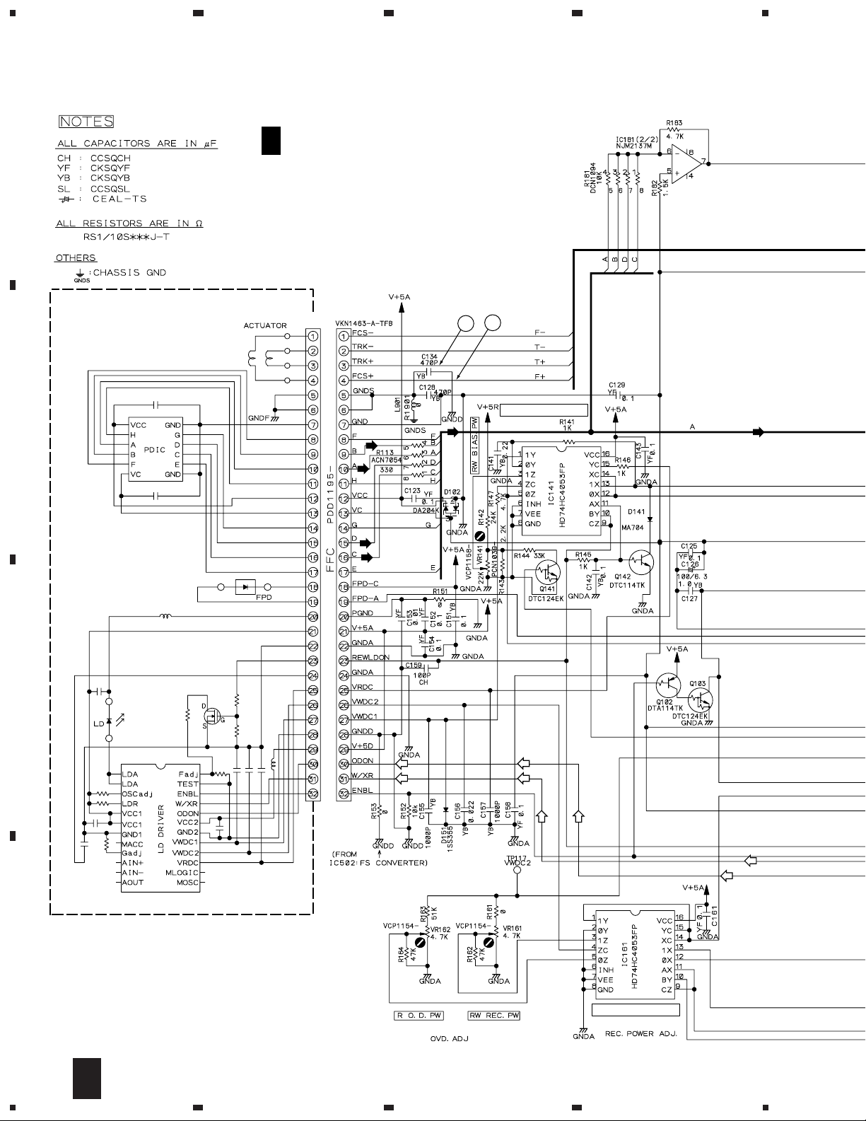
3.8 CD-R CORE (5/5), SERVO MECHANISM, LOADING A and LOADING B
ASSYS
A
A 5/5
CD-R CORE ASSY (PYY1273)
• DECODER BLOCK
A 3/5
5ch ACTUATOR DRIVER
CN453
B
CN451
CN452
1 2
3
C
CN501
S501
LOADING A
C
ASSY (PWZ3760)
LOADING B
D
ASSY (PWZ3761)
CN551
CARRIAGE MOTOR
ASSY (SLIDER)
CN601
D
PEA1350
DC MOTOR ASSY
(SPINDLE)
PEA1235
S601
SERVO MECHANISM
B
ASSY (PWZ3759)
LOADING MOTOR
ASSY
VXX2505
PC651
NJL5803K-F1
J601
A 2/5
24
5/5
A
1234
B C D
Page 25

5
678
PDR-L77
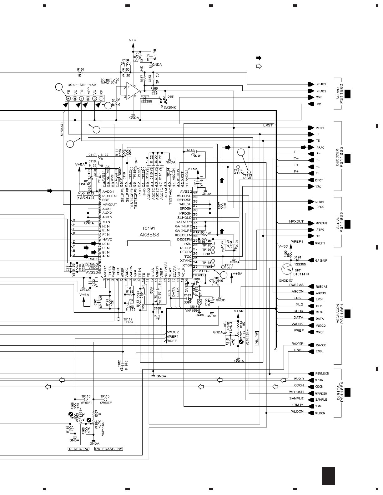
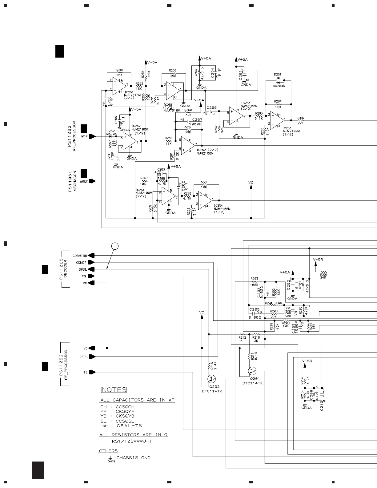
A 2/5
A
A 1/5
5
B
4
CD DECODER
CN901
A 4/5
C
CN7002
G
D
: RF SIGNAL ROUTE
: AUDIO SIGNAL ROUTE
: The power supply is shown with the marked box.
5
6
5/5
A
7
8
25
Page 26

1
PDR-L77
3.9 CDR ASSY
23
4
A
B
CDR ASSY
E
(AWM7486)
CN7704
(DI)
(DO)
(AR)
(PB)
(PB)(PB)
(PB)
(PB)
CN7201
F
(AR)
(AR)
C
CN7502
(AR)
CN7502
H
(REC)
D
26
1234
Page 27

(PB)
5
678
PDR-L77
SIGNAL ROUTE
(AR)
: ANALOG REC SIGNAL
(REC)
: REC SIGNAL (after A/D)
(PB)
(PB)
: PB OUT SIGNAL (before D/A)
(PB)
: PB OUT SIGNAL
(DI)
: DIGITAL INPUT SIGNAL
(DO)
: DIGITAL OUT SIGNAL
(REC)
A
(PB)
(DI1)
(PB)
(DO)
CN7701
CN7702
CN501CN301
A 4/5A 4/5
B
C
(REC)
D
27
5
6
7
8
Page 28

1
23
PDR-L77
3.10 PWSB and PJB ASSYS
4
A
PWSB ASSY
G
(KUXJ/CA : AWU7521)
(MYXJ, NVXJ : AWU7537)
(AI)
5.0
5.0
(PB)
B
10.3
FAN
-12.8
C
VEC-063
5.0
VEC-063
D
-26.9
• NOTE FOR FUSE REPLACEMENT
CAUTION -
FOR CONTINUED PROTECTION AGAINST RISK OF FIRE.
REPLACE WITH SAME TYPE AND RATINGS ONLY.
28
1234
Page 29

5
678
PDR-L77
A
SIGNAL ROUTE
(AI)
: ANALOG INPUT SIGNAL
(PB)
: PB OUT SIGNAL
(DI)
: DIGITAL INPUT SIGNAL
(DO)
: DIGITAL OUT SIGNAL
CN7002
CN901
E
CN7704
A 5/5
B
(AI)
-5.1
(PB)
CN7003
CN7201
CN7202
F
(AI)
(PB)
PJB ASSY
(AWU7524)
(AI)
(PB)
(DO)
(DI)
C
(DO)
(DI)
D
29
5
6
7
8
Page 30

1
PDR-L77
3.10 FLDP and FRKB ASSYS
A
FRKB ASSY
I
(AWU7523)
23
4
CN7501
B
CN7502
J7501
E
C
CN7502
D
FLDP ASSY
H
(AWU7522)
30
1234
Page 31

5
678
PDR-L77
A
B
64 63 62 61 60 59 58 57 56 55 54 53 52 51 50 49
148
2
3
4
5
6
7
8
9
10
11
12
13
14
15
16
17 18 19 20 21 22 23 24 25 26 27 28 29 30 31 32
FL DRIVER
47
46
45
44
43
42
41
40
39
38
37
36
35
34
33
C
D
31
5
6
7
8
Page 32

PDR-L77
VOLTAGES and WAVEFORMS
CD-R CORE ASSY
A 1/5
Media Pickup Position
12cm Inner 0V 0V
12cm Outer 5V 0V
CD
8cm Inner 0V 0V
8cm Outer 5V 0V
12cm Inner 5V 0V
CD-R
CD-RW
12cm Outer 5V 0V
8cm Inner 0V 5V
8cm Outer 5V 5V
at FS = 44 kHz
(at FS Converter through)
FSR/XTHR
(CN301-pin 2)
at DIGITAL LOCK at DIGITAL UNLOCK
XVCO
(CN301-pin3)
UNLOCK
(CN301-pin7)
XPFAIL
(CN301-pin4)
XRST
(CN301-pin11)
0V 5V
0V 5V
0V 5V
5V
5V
DGAI
(IC351-pin56)
D8CM
(IC351-pin57)
Others
−
−
Note :
The encircled numbers denote measuring point in the schematic diagram.
CD-R CORE ASSY
A 1/5
CN301 - pin 5 (MREQ)
1
V: 0.2V/div.(10 : 1) H: 5msec/div.
(STOP)
CN301 - pin 6 (EN_CE)
2
V: 0.2V/div.(10 : 1) H: 5msec/div.
(STOP)
CN301 - pin 8 (XFUSE)
3
V: 0.2V/div.(10 : 1) H: 5msec/div.
(STOP)
CN301 - pin 13 (MSI)
7
V: 0.2V/div.(10 : 1) H: 5msec/div.
(STOP)
IC301 - pin 28 (SCLK)
8
V: 2V/div. H: 2µsec/div.
(Disck Loading)
IC301 - pin 27 (XL2)
9
V: 0.2V/div.(10 : 1) H: 5msec/div.
(STOP)
CD-R CORE ASSY
A 3/5
Operating
Mode
CLV
(IC201-pin13)
ECLV
(IC201-pin14)
STOP 0V 0V
CAV 0V 5V
CLV 5V 0V
ECLV 5V 5V
CD-R CORE ASSY
A 4/5
A/D Converter used
ADSTBY
(CN501-pin4)
AMUTE
(CN501-pin9)
LRSTD
(CN501-pin10)
at Analog REC Pause
or REC
0V 5V
at MUTE ON
(Audio Signal Not Output)
5V 0V
5V −
Others
at MUTE OFF
(Audio Signal Output)
CN301 - pin 9 (MACK)
4
V: 0.2V/div.(10 : 1) H: 5msec/div.
(STOP)
CN301 - pin 10 (MSCK)
5
V: 0.2V/div.(10 : 1) H: 0.5µsec/div.
(PLAY)
CN301 - pin 12 (MSO)
6
V: 0.2V/div.(10 : 1) H: 5msec/div.
(STOP)
IC301 - pin 26 (DATA)
10
V: 0.2V/div.(10 : 1) H: 5msec/div.
(STOP)
IC301 - pin 25 (CLOK)
11
V: 0.2V/div.(10 : 1) H: 5msec/div.
(STOP)
IC301 - pin 24 (XLAT)
12
V: 0.2V/div.(10 : 1) H: 5msec/div.
(STOP)
32
Page 33

PDR-L77
CD-R CORE ASSY
A 2/5
CN102 - pin 1 (RF)
1
V: 20mV/div.(10 : 1) H: 0.5µsec/div.
(PLAY)
CN102 - pin 3 (MPP)
2
V: 10mV/div.(10 : 1) H: 2msec/div.
(PLAY)
CN102 - pin 4 (TE)
3
V: 5mV/div.(10 : 1) H: 2msec/div.
(PLAY)
TP113 (RFAC)
5
V: 0.2V/div.(10 : 1) H: 0.2µsec/div.
(PLAY)
IC101 - pin 22 (ATFG)
6
V: 0.2V/div. H: 20µsec/div.
(REC)
CN101 - pin 3 (TRK +)
7
V: 0.2V/div.(10 : 1) H: 5msec/div.
(STOP)
CD-R CORE ASSY
A 3/5
TP210 (FG)
1
V: 0.2V/div.(10 : 1) H: 1msec/div.
(PLAY)
Foot of R212 (SPDL)
2
V: 20mV/div. H: 2msec/div.
(PLAY)
CN102 - pin 6 (FE)
4
V: 5mV/div.(10 : 1) H: 2msec/div.
(PLAY)
CN101 - pin 4 (FCS +)
8
V: 0.2V/div.(10 : 1) H: 5msec/div.
(STOP)
33
Page 34

PDR-L77
CD-R CORE ASSY
A 4/5
CN501 - pin 2 (ADBCK)
1
V: 0.2V/div.(10 : 1) H: 0.2µsec/div.
(STOP)
CN501 - pin 3 (ADDATA)
2
V: 0.2V/div.(10 : 1) H: 0.2µsec/div.
(REC)
CN501 - pin 5 (ADLRCK)
3
V: 0.2V/div.(10 : 1) H: 10µsec/div.
(STOP)
CN501 - pin 14 (DABCK)
7
V: 0.2V/div.(10 : 1) H: 0.2µsec/div.
(STOP)
CN501 - pin 16 (DALRCK)
8
V: 0.2V/div.(10 : 1) H: 10µsec/div.
(STOP)
CN501 - pin 18 (DIN1)
9
V: 0.2V/div.(10 : 1) H: 0.2µsec/div.
(REC_OPTICAL)
IC501 - pin 88 (EFM)
13
V: 0.2V/div.(10 : 1) H: 0.5µsec/div.
(REC)
IC431 - pin 6 (17M)
14
V: 0.2V/div.(10 : 1) H: 50msec/div.
(REC)
IC431 - pin 25 (ODON)
15
V: 0.2V/div.(10 : 1) H: 0.1µsec/div.
(REC)
CD-R CORE ASSY
A 5/5
CN452 - pin 2 (SL +)
1
V: 0.2V/div.(10 : 1) H: 5msec/div.
(PLAY)
CN452 - pin 3 (SP +)
2
V: 0.2V/div.(10 : 1) H: 5msec/div.
(PLAY)
CN452 - pin 9 (FG)
3
V: 0.2V/div.(10 : 1) H: 1msec/div.
CN501 - pin 7 (MCK)
4
V: 0.1V/div.(10 : 1) H: 50msec/div.
(STOP)
CN501 - pin 12 (CL)
5
V: 0.2V/div.(10 : 1) H: 0.5µsec/div.
(STOP)
CN501 - pin 13 (DADATA)
6
V: 0.2V/div.(10 : 1) H: 0.5µsec/div.
(PLAY)
CN501 - pin 19 (DITOUT)
10
V: 0.2V/div.(10 : 1) H: 0.2µsec/div.
(STOP)
CN501 - pin 20 (DIN2)
11
V: 0.2V/div.(10 : 1) H: 0.2µsec/div.
(REC_Coaxial)
CN501 - pin 11 (DI)
12
V: 0.2V/div.(10 : 1) H: 5msec/div.
(STOP)
IC431 - pin 29 (WLDON)
16
V: 0.2V/div.(10 : 1) H: 1msec/div.
(REC)
IC431 - pin 34 (REWLDON)
17
V: 0.2V/div.(10 : 1) H: 1msec/div.
(REC)
TP503 (W/XR)
18
V: 0.2V/div.(10 : 1) H: 1msec/div.
(REC)
IC401 - pin 25 (MDP)
4
V: 0.2V/div.(10 : 1) H: 5µsec/div.
(PLAY)
IC401 - pin 25 (MDP)
V: 0.2V/div.(10 : 1) H: 5µsec/div.
(REC)
IC401 - pin 20 (MIRR)
5
V: 0.2V/div.(10 : 1) H: 20µsec/div.
(REC_CD-RW)
34
Page 35

1
234
4. PCB CONNECTION DIAGRAM
4.1 SERVO MECHANISM, LOADING A and LOADING B ASSYS
NOTE FOR PCB DIAGRAMS :
1. Part numbers in PCB diagrams match those in the schematic
diagrams.
2. A comparison between the main parts of PCB and schematic
diagrams is shown below.
Symbol In PCB
Diagrams
BCE
BCE
D
Symbol In Schematic
Diagrams
BCEBCE
BCE
BCE
DGGSS
DGS
Part Name
Transistor
Transistor
with resistor
Field effect
transistor
Resistor array
3-terminal
regulator
3. The parts mounted on this PCB include all necessary parts for
several destinations.
For further information for respective destinations, be sure to
check with the schematic diagram.
4. View point of PCB diagrams.
Connector
Capacitor
SIDE A
P.C.Board
Chip Part
SIDE B
PDR-L77
A
CARRIAGE
MOTOR
M
SPINDLE
MOTOR
SERVO
B
MECHANISM
ASSY
M
CN452
A
C
LOADING A
ASSY
SERVO
B
MECHANISM
ASSY
LOADING A
C
ASSY
B
C
LOADING B
D
ASSY
1
CN451
A
LOADING B
LOADING
MOTOR
D
ASSY
A
M
SIDE A SIDE B
2
CN453
(PNP1471-B)
3
D
DCB
4
35
Page 36

1
PDR-L77
4.2 CD-R CORE ASSY
A
CD-R CORE ASSY
A
B
23
• This PCB is a four-layered board.
4
D
CN551
C
CN501
B
CN601
J
CN21
E
CN804
To
CD-R
PICKUP
C
E
CN801
(PNP1465-B)
VR164
VR161 VR141 VR162 VR163 VR101
IC361-IC364 IC303 IC302 IC305IC931-IC933
IC351 IC371 IC301 IC304 IC503Q301
D
Q302 Q303 Q402 Q401 IC401 IC501 IC507 IC506IC352
IC451 IC201 IC502 IC509Q203 Q203IC251-IC254
Q201 IC101 Q142 IC562 IC431
36
SIDE A
A
1234
Page 37

1
234
PDR-L77
CD-R CORE ASSY
A
• This PCB is a four-layered board.
A
B
Q551 Q202 IC255
IC505 IC508 IC181
Q102 IC561 IC141 IC161
Q103 Q141
SIDE B
1
2
C
(PNP1465-B)
D
A
3
4
37
Page 38

1
PDR-L77
4.3 CDR ASSY
23
4
A
E
CDR ASSY
F
CN7201
SIDE A
A
CN501
B
C
D
A
CN301
H
CN7502
38
E
(ANP7336-B)
IC7451Q7423 Q7513
1234
Q7451
Q7454
Q7453
Q7101
Q7103
Q7104
Q7509–Q7511
IC7501
Q7512
Page 39

SIDE B
1
234
PDR-L77
A
E
CDR ASSY
B
(ANP7336-B)
1
Q7107
Q7508
Q7507
IC7101 Q7301
Q7105
IC7102
Q7505
Q7506
Q7502
Q7501
2
IC7301
Q7246
Q7245
3
Q7241
IC7241
IC7401
E
4
C
D
39
Page 40

1
PDR-L77
4.4 PJB ASSY
23
4
A
F
PJB ASSY
SIDE A
B
G
CN7003
(ANP7337-B)
F
PJB ASSY
E
CN7704
SIDE B
C
D
40
F
1234
Page 41

1
4.5 FRKB ASSY
234
PDR-L77
A
SIDE A
(ANP7337-B)
I
FRKB ASSY (1/3)
I
FRKB ASSY (2/3)
I
FRKB ASSY (3/3)
H
J7501
B
SIDE B
I
FRKB ASSY (1/3)
I
FRKB ASSY (3/3)
I
FRKB ASSY (2/3)
C
D
41
I
1
2
3
4
Page 42

1
PDR-L77
4.6 PWSB ASSY
A
Q7007
IC7005IC7006
B
G
PWSB ASSY
23
F
CN7202
A
CN901
4
SIDE A
Q7010
Q7008
DC FAN
MOTOR
(ANP7337-B)
C
IC7052
D
AC
POWER
CORD
42
G
1234
Page 43

SIDE B
1
234
PDR-L77
G
PWSB ASSY
Q7006
A
B
(ANP7337-B)
Q7009
C
Q7051
D
G
1
2
3
4
43
Page 44

A
B
1
PDR-L77
4.7 FLDP ASSY
I
CN7501
23
H
FLDP ASSY (1/2)
4
SIDE A
C
E
CN7502
D
44
H
1234
(ANP7337-B)
H
FLDP ASSY (2/2)
Page 45

SIDE B
1
234
PDR-L77
H
FLDP ASSY (1/2)
A
B
H
FLDP ASSY (2/2)
1
(ANP7337-B)
2
C
D
H
3
4
45
Page 46

PDR-L77
5. PCB PARTS LIST
NOTES : Parts marked by “ NSP ” are generally unavailable because they are not in our Master Spare Parts List.
The mark found on some component parts indicates the importance of the safety factor of the part.
Therefore, when replacing, be sure to use parts of identical designation.
When ordering resistors, first convert resistance values into code form as shown in the following examples.
Ex. 1 When there are 2 effective digits (any digit apart from 0), such as 560 ohm and 47k ohm (tolerance is shown by
J = 5%, and K = 10%).
560 Ω = 56 × 10
47k Ω = 47 × 10
0.5 Ω = R50 ...................................................................... RN2H Â 5 0 K
1 Ω = 1R0 ......................................................................... RS1P 1 Â 0 K
Ex. 2 When there are 3 effective digits (such as in high precision metal film resistors).
5.62k Ω = 562 × 10
LIST OF WHOLE PCB ASSEMBLIES
Mark Symbol and Desacription
CD-R CORE ASSY
NSP
MECHANISM ASSY
NSP
SERVO MECHANISM ASSY
NSP
LOADING A ASSY
NSP
LOADING B ASSY
1
= 561................................................... RD1/4PU 5 6 1 J
3
= 473 .................................................. RD1/4PU 4 7 3 J
1
= 5621 ........................................... RN1/4PC 5 6 2 1 F
Part No.
KUXJ/CA type MYXJ type NVXJ type
PYY1273
PWX1570
PWZ3759
PWZ3760
PWZ3761
PYY1273
PWX1570
PWZ3759
PWZ3760
PWZ3761
PYY1273
PWX1570
PWZ3759
PWZ3760
PWZ3761
Remarks
NSP
CDR ASSY
NSP
COMPLEX ASSY
PJB ASSY
PWSB ASSY
FLDPASSY
FRKB ASSY
AWM7486
AWM7496
AWU7524
AWU7537
AWU7522
AWU7523
AWM7486
AWM7487
AWU7524
AWU7521
AWU7522
AWU7523
AWM7486
AWM7487
AWU7524
AWU7521
AWU7522
AWU7523
Mark No. Description Part No. Mark No. Description Part No.
IC301 PE5109B
CD-R CORE ASSY
SEMICONDUCTORS
IC502 AD1893JST
IC101 AK8563
IC321 BA05FP
IC561 BA7082F
IC303 (BR93LC46F) PYY1196
IC401 CXD2585Q
IC141, IC161, IC255, IC508 HD74HC4053FP
IC371 HD74HC573FP
IC501 LC89585
IC503 LH64256CK-70
IC931 LP2980IM5-5.0
IC451 M56788FP
IC252–IC254 NJM2100M
IC181 NJM2137M
IC304 NJM2904M
IC932 PST994C
IC362 TC7S00F
IC363, IC562 TC7S04F
IC305, IC509 TC7S08F
IC361, IC364 TC7S14F
IC302 TK11041M-1
Q102 DTA114TK
Q204, Q401, Q402 DTA124EK
Q551 DTA143EK
Q101, Q142, Q201–Q203 DTC114TK
Q103, Q141, Q301–Q303 DTC124EK
D101, D151, D182, D201, D302 1SS355
D321, D322, D361, D362 1SS355
D102, D181, D202, D251 DA204K
D551 DAN202K
D301 DAP202K
D141, D252, D323 MA704
D204 UDZ3.0B
IC251 NJU7016M
IC201 PA9007A
IC507 PCX1026
IC351 PDJ014A
IC431 PDK041A
46
Page 47

PDR-L77
Mark No. Description Part No. Mark No. Description Part No.
COILS AND FILTERS
L434, L505 CHIP COIL DTL1058
L101, L302, L305–L309 OTL1040
CHIP SOLID INDUCTOR
L311–L315, L318, L319 OTL1040
CHIP SOLID INDUCTOR
L322–L324, L351, L371 OTL1040
CHIP SOLID INDUCTOR
L511–L513, L515–L518, L522 OTL1040
CHIP SOLID INDUCTOR
L524, L526 OTL1040
CHIP SOLID INDUCTOR
L568 CHIP SOLID INDUCTOR QTL1015
F401, F403, F432, F433 VTF1097
CHIP SOLID INDUCTOR
F501–F504, F506–F508, F510 VTF1097
CHIP SOLID INDUCTOR
F514, F520, F521, F527 VTF1097
CHIP SOLID INDUCTOR
F551, F552, F561 VTF1097
CHIP SOLID INDUCTOR
CAPACITORS
C122, C507
C159, C434, C551, C564 CCSQCH101J50
C508 CCSQCH120J50
C563 CCSQCH160J50
C406 CCSQCH221J50
C107, C404 CCSQCH331J50
C263, C311 CCSQCH470J50
C213, C256, C408 CCSQCH471J50
C418 CCSQCH681J50
C101
C518 CCSQCH820J50
C183, C184
C480–C482 CCSQSL471J50
C321, C465, C931 CEAL100M50
C121, C126, C327, C401, C409 CEAL101M6R3
C417, C901, C902 CEAL101M6R3
C307 CEAL1R0M50
C216 CEAL2R2M50
C933 CEAL3R3M50
C181, C452, C477, C903 CEAL470M16
C130, C201, C209, C211, C253 CEAL470M6R3
C323, C368, C431, C502, C512 CEAL470M6R3
C515, C520, C553, C559, C566 CEAL470M6R3
C308 CEAL4R7M50
C155, C157, C207, C233, C257 CKSQYB102K50
C403, C407, C501, C517 CKSQYB102K50
C109, C110, C112, C230, C231 CKSQYB103K50
C251, C324, C412, C454–C459 CKSQYB103K50
C470–C473, C505, C510, C558 CKSQYB103K50
C567, C934 CKSQYB103K50
CCSQCH100D50
CCSQCH6R0D50
CCSQCJ3R0C50
C208, C414 CKSQYB152K50
C451 CKSQYB182K50
C156, C203 CKSQYB223K50
C113–C115, C117, C118 CKSQYB224K16
C304, C305, C460, C462 CKSQYB224K16
C212 CKSQYB272K50
C104, C221 CKSQYB331K50
C103 CKSQYB333K50
C131, C215, C227–C229 CKSQYB334K16
C128, C134, C363, C474, C475 CKSQYB471K50
C206, C413 CKSQYB473K25
C102 CKSQYB473K50
C119, C204, C468, C469 CKSQYB681K50
C463, C464 CKSQYB682K50
C205 CKSQYB823K25
C133, C153, C254, C303, C322 CKSQYF103Z50
C362, C416, C433, C519 CKSQYF103Z50
C521, C522, C555, C561, C562 CKSQYF103Z50
C568, C569, C905 CKSQYF103Z50
C106, C108, C111, C120, C123 CKSQYF104Z25
C125, C129, C132, C143, C152 CKSQYF104Z25
C154, C158, C161, C202, C210 CKSQYF104Z25
C214, C217, C255, C260–C262 CKSQYF104Z25
C301, C302, C306, C309, C310 CKSQYF104Z25
C312, C313, C326, C365–C367 CKSQYF104Z25
C369, C371, C402, C405 CKSQYF104Z25
C410, C411, C415, C432 CKSQYF104Z25
C466, C467, C503, C506, C509 CKSQYF104Z25
C511, C513, C516, C523, C552 CKSQYF104Z25
C554, C560, C565 CKSQYF104Z25
C124, C328, C570, C904 CKSQYF473Z25
C325 (1F/5.5V) VCH1039
RESISTORS
R113, R441, R442, R514 (330Ω) ACN7054
R308, R417 (470Ω) ACN7056
R313 (47kΩ) ACN7077
R401, R416, R433 (100Ω) DCN1092
R507 (220Ω) DCN1093
R181, R371, R372, R501 (10kΩ) DCN1094
R570 (0Ω) DCN1106
R143 (2.2kΩ) PCN1039
VR101, VR161–VR164 (4.7kΩ) VCP1154
VR141 (22kΩ) VCP1158
Other Resistors RS1/10S&&&J
OTHERS
CN453 CONNECTOR POST B2B-PH-K-S
CN451 CONNECTOR POST B3B-PH-K-S
CN901 CONNECTOR S6B-PH-K-S
CN301 15P CONNECTOR VKN1275
CN501 21P CONNECTOR VKN1281
C142, C151, C182, C224–C226 CKSQYB104K25
C361, C364, C453, C476, C504 CKSQYB104K25
C932 CKSQYB104K25
C105, C116, C127, C232, C258 CKSQYB105K10
C514, C557 CKSQYB105K10
CN101 32P CONNECTOR VKN1463
KN101, KN321, KN501, KN901 VNF1084
EARTH METAL FITTING
X501 (16.9344MHz) PSS1008
X301 (32.00MHz) PSS1023
47
Page 48

PDR-L77
Mark No. Description Part No. Mark No. Description Part No.
CAPACITORS
SERVO MECHANISM ASSY
SEMICONDUCTORS
PC651 NJL5803K-F1
SWITCHES AND RELAYS
S601 PSG1013
RESISTORS
All Resistors RD1/4PU&&&J
OTHERS
J601 3P JUMPER WIRE D20PWW0305E
CN601 CONNECTOR POST S9B-PH-K-S
LOADING A ASSY
SWITCHES AND RELAYS
501 VSK1011
OTHERS
CN501 CONNECTOR POST S3B-PH-K-S
LOADING B ASSY
OTHERS
CN551 CONNECTOR POST B2B-PH-K-S
CDR ASSY
C7101, C7102, C7117, C7118 CCSRCH101J50
C7413, C7414, C7507, C7516 CCSRCH101J50
C7103, C7104 CCSRCH220J50
C7107, C7108 CCSRCH470J50
C7105, C7106, C7109, C7110 CEV100M16
C7119, C7120, C7241, C7242, C7504 CEV100M16
C7253, C7254 CEV100M35
C7243, C7244 CEV100M50
C7306, C7311, C7402, C7407 CEV101M6R3
C7411, C7412, C7509 CEV101M6R3
C7301, C7302 CEV2R2M50
C7111, C7112, C7121 CEV330M6R3
C7303, C7304, C7403, C7404 CEV4R7M35
C7409 CKSRYB102K50
C7313, C7505, C7508, C7512, C7513 CKSRYB103K50
C7597, C7598 CKSRYB103K50
C7307, C7308 CKSRYB471K50
C7249–C7252 CKSRYB681K50
C7113, C7114, C7305, C7309, C7310 CKSRYF104Z25
C7312, C7401, C7405, C7406, C7408 CKSRYF104Z25
C7410, C7416, C7451, C7506 CKSRYF104Z25
C7510, C7511, C7514 CKSRYF104Z25
RESISTORS
R7545 RS1/10S0R0J
R7129, R7130, R7267, R7268 RS1/8S330J
Other Resistors RS1/16S&&&J
OTHERS
CN7702 15P CONNECTOR VKN1501
CN7502 16P CONNECTOR VKN1502
CN7701 21P CONNECTOR VKN1507
CN7704 25P CONNECTOR VKN1511
X7501 (4.19MHz) DSS1105
SEMICONDUCTORS
IC7101,IC7102,IC7241 BA4558F-HT
IC7401 PCM1716E
IC7301 PCM1800-1
IC7501 PE5138A
IC7451 TC7SU04F
Q7501, Q7502 2SA1576A
Q7103, Q7104, Q7503 2SC4081
Q7107, Q7246, Q7506, Q7507 DTA124EU
Q7512, Q7513 DTA124EU
Q7301, Q7451, Q7504, Q7508 DTC124EU
Q7101, Q7105, Q7241 UMX1N
D7301, D7401 1SS184
D7101, D7102, D7403, D7404, D7501 1SS355
D7241, D7302, D7402 DAP202K
COILS AND FILTERS
L7301, L7401, L7501 OTL1040
CHIP SOLID INDUCTOR
48
PJB ASSY
COILS AND FILTERS
L7601 LFA100J
CAPACITORS
C7611, C7612 CEAT100M50
C7602 CEAT101M10
C7601, C7604 CKSQYB103K50
RESISTORS
All Resistors RS1/10S&&&J
OTHERS
JA7601 OPTICAL RECEIV MOD. GP1F37R
CN7202 20P SOCKET KP200IB20L
JA7602 OPTICAL OUTPUT JACK TOTX178
7002 PCB BINDER VEF1040
CN7201 25P CONNECTOR VKN1201
Page 49

PDR-L77
Mark No. Description Part No. Mark No. Description Part No.
T7001 STANDBY TRANSFORMER ATT7049
PWSB ASSY
(1) CONTRAST TABLE
AWU7537 and AWU7521 are constructed the same except
for the following :
AKP7032
ATT7049
Part No.
BKP1046
ATT7056
Remarks
Mark
Symbol and
Description
AN101 POWER SOCKET
T7001 STANDBY TRANS.
AWU7537 AWU7521
(2) PARTS LIST FOR AWU7537
SEMICONDUCTORS
IC7005,IC7006 BA05T
IC7052 NJM78M05FA
Q7006, Q7009 2SA1037K
Q7008 2SB1238X
Q7011, Q7051 2SC2412K
CN7001 CONNECTOR POST B2B-PH-K-S
CN7002 CONNECTOR B6B-PH-K-S
SCREW BBZ30P080FCC
JA7201, JA7202 JACK BKB1017
J7001 6P JUMPER WIRE D20PYY0605E
CN7003 20P PLUG KM200IB20
JA7603 JACK RKN1026
7003 PCB BINDER VEF1040
KN7001 EARTH METAL FITTING VNF1084
FLDP ASSY
SEMICONDUCTORS
IC7551 MSM9202-01
D7510 1SS355
D7554
SLR-343VC(NPQ)
Q7007, Q7010 2SD1858X
D7005, D7006, D7010, D7055–D7057 1SS355
D7001 D3SBA20(B)
D7013, D7014 MTZJ6.8B
D7051 S1WB(A)60SD
D7012 S5566G(TPB2)
D7009 UDZ4.7B
COILS AND FILTERS
L7001 LINE FILTER ATF7024
SWITCHES AND RELAYS
RY7001 ASR7018
CAPACITORS
C101, C7023 (10000pF/AC250V) ACG7033
C7203–C7210 CCSQCH101J50
C7006, C7015, C7016, C7022, C7053 CEAT100M50
C7009, C7011 CEAT101M10
C7052 CEAT102M16
C7013 CEAT221M50
C7002 CEAT471M16
C7608, C7609 CKSQYB102K50
C7012, C7021 CKSQYB103K50
C7201, C7202, C7606 CKSQYF104Z25
C7020 CQMA103K2E
C7018, C7019, C7051 CQMBA103J50
C7007(6800µF/16V) VCH1060
RESISTORS
R7010 RD1/4VM123J
R7026 RFA1/4PL4R7J
Other Resistors RS1/10S&&&J
COILS AND FILTERS
L7501 LCTB100K2125
SWITCHES AND RELAYS
S7501–S7504, S7506 ASG7013
CAPACITORS
C7564, C7567, C7568, C7574 CCSQCH101J50
C7565 CCSQCH470J50
C7555 CEJA100M50
C7561 CEJA101M6R3
C7571 CEJA470M6R3
C7573, C7580 CKSQYB103K50
C7551, C7553 CKSQYB473K50
C7563, C7569 CKSQYF104Z25
C7566 CKSQYF104Z50
RESISTORS
All Resistors RS1/10S&&&J
OTHERS
3P CABLE HOLDER 51048-0300
4P CABLE HOLDER 51048-0400
12P CABLE HOLDER 51048-1200
13P CABLE HOLDER 51048-1300
V7001 FL TUBE AAV7074
FL SPACER AEB7069
J7506 JUMPER WIRE D20PYY0305E
J7501 JUMPER WIRE D20PYY0405E
7551 REMOTE RECEIVER UNIT GP1U26X
CN7502 16P CONNECTOR VKN1276
OTHERS
6P CABLE HOLDER 51048-0600
1, 2 COVER AEC-294
AN101 POWER SOCKET AKP7032
H101, H102 FUSE CLIP AKR7001
7005, 7006 HEAT SINK M ANH-697
49
Page 50

PDR-L77
Mark No. Description Part No.
FRKB ASSY
SEMICONDUCTORS
D7552 EB3804X(BCDE)
D7555
D7553 UDZS8.2B
SWITCHES AND RELAYS
S7505, S7507 ASG7013
RESISTORS
All Resistors RS1/10S&&&J
OTHERS
3P CABLE HOLDER 51048-0300
CN7501 4PJUMPER CONNECTOR 52151-0410
J7503 JUMPER WIRE D20PYY0210E
J7502 JUMPER WIRE D20PYY0325E
SLR-343MC(NPQ)
50
Page 51

6. ADJUSTMENT
PDR-L77
6.1 DISCS TO BE USED
1. When adjusting the servo system adjustment
CD : Test disc for adjustment (STD-903 or equivalent)
6.2 JIGS AND MEASURING
INSTRUMENTS
(1) Laser Power Meter
Following power meter manufactured by Advantest Corporation
or equivalent :
TQ8210 + TQ82017
TQ8215 + TQ82021
TQ8215 + TQ82010 + TQ82017
LE8010 (by LEADER)
(2) Oscilloscope
(3) CD Jitter Meter
(4) Remote control supplied with PDR-L77 (AXD7242)
[(5)LD service remote control (GGF1067)]
6.3 TEST MODE
6.3.1 Test Mode
For adjustment, set the unit to Test mode. To enter Test mode, turn
on the unit with the Test Mode Short-Circuit pattern on the CDR
Assy. In Test mode, the display (FL) on the unit lights as follows.
0 00 00´00´´
If not, turn the power off and repeat the same steps again.
6.3.2 Operations in Test Mode
Please use the remote control provited with the PDR-L77(AXD7242)
or the LD service remote control(GGF1067).
In Test mode, the following adjustment functions are assigned to
the buttons, as explained below.
7 During adjustment of LD power
(“DIGITAL” segment does not light this time)
COMPACT DISC RECORDER
ERASE button
(TV/LDP button)
: Switching CD/CD-R/CD-RW
(STOP/OPEN CLOSE button)
INPUT SELECTOR button
STOP button
: LD off
(DIG/ANA button)
: Test mode switch
Fig.2 During adjustment of LD power
REMOTE CONTROL UNIT
CU–PD113
Î
@ STANDBY/ON
FADER
FINALIZE
DIGITAL
AUTO/
ERASE
SYNCHRO
SELECTOR
PROGRAM
MANUAL
&
*#
!
⁄
INPUT
SKIP PLAY
SET CLEAR
1526374
9
10/0 >10
CHECK
CLEAR
• ‡
TRACK NO.
WRITE
TIME
$›
SKIP ID
REPEAT
RANDOM
REC MUTE button
(SIDE B button)
: LD on 2
REC
RECORD button
(SIDE A button)
: LD on 1
1, ¡ button
(4, ¢ button)
: Sled move
8
AXD7242
(The button shown in
corresponds in GGF1067.)
CDR ASSY
SIDE B
Fig. 1 Enter the Test mode
Short-circuit
7 During adjustment of servo system
(“DIGITAL” segment lights this time)
FINALIZE button
(REP. A button)
: Focus in
ERASE button
(TV/LDP button)
: Adjustment value decision
DIGITAL SYNCHRO button
(STILL STEP e button)
: Adjustment value decision
(STOP/OPEN CLOSE button)
INPUT SELECTOR button
STOP button
: Stop
PAUSE button
(PAUSE button)
: Tracking servo close
(DIG/ANA button)
: Test mode switch
1, ¡ button
(4, ¢ button)
: Sled move
Fig.3 During adjustment of servo system
COMPACT DISC RECORDER
REMOTE CONTROL UNIT
CU–PD113
Î
@ STANDBY/ON
FINALIZE
FADER
DIGITAL
SYNCHRO
SELECTOR
PROGRAM
AUTO/
ERASE
MANUAL
&
*#
!
⁄
INPUT
SKIP PLAY
SET CLEAR
1526374
9
10/0 >10
CHECK
CLEAR
• ‡
REC
TRACK NO.
WRITE
TIME
$›
SKIP ID
8
REPEAT
RANDOM
REC MUTE button
(SIDE B button)
: Adjustment
RECORD button
(SIDE A button)
: Adjustment
AUTO/MANUAL,
TRACK No. WRITE button
(CX button)
: Servo adjustment mode switch
PLAY button
(PLAY button)
: Spindle kick
CLEAR button
(X3 3 button)
: Adjustment value initialization
BET button
(TV/LDP button)
: Adjustment value decision
AXD7242
(The button shown in
corresponds in GGF1067.)
51
Page 52

PDR-L77
6.4 ADJUSTMENT 1 (LASER DIODE POWER ADJUSTMENT)
CD-R CORE ASSY
RW ERASE
VR164
VR141
RW BIAS
VR161
RW REC
VR162
R O.D.
VR163
R REC
VR101
PB. PW
CN102
6
1
1 : RF
2 : VC
3 : MPP
4 : TE
5 : VC
6 : FE
CD-R overdrive
CD-R record
power
Playback power
Playback CD-R recording
CD-RW erase
power
CD-RW record power
CD-RW bias
power
CD-RW recording
Fig.5 Output power of the laser diode
Note 1 : Attach the remote sensor of the laser power meter to a
Note 2 : When adjusting with VRs, first turn them completely
Note 3 : The wave length setting of the laser power meter is
assumed to be 780nm.
point angled away about 10 degrees against the pickup
lens and where the maximum power is detected, so that
there will be no light reflected onto the pickup.
counter-clockwise and then adjust clockwise, so that the
value to be reached is not exceeded.
Fig. 4 Adjustment points
DANGER – LASER RADIATION WHEN OPEN.
6.4.1 Playback Power Adjustment
Test Point
Adjustment Point
Adjustment Value
[Procedure]
(1) Check that "CD" is displayed on the FL display. If "CD-R" or "CD-RW" is displayed, press the ERASE button repeatedly until "CD" is
displayed.
(2) Press the RECORD button.
(3) Press the REC MUTE button. The LED for confirmation of LD emission will light in red. The LD is emitting in this status.
(4) Turn VR101 clockwise until the adjustment value to be reached is obtained.
(5) Press the STOP button to shut off the LD.
Pickup objective lens
VR101 (PB. PW)
0.60 mW ± 0.05 mW
AVOID DIRECT EXPOSURE TO BEAM.
52
Page 53

6.4.2 CD-R Record Power Adjustment
PDR-L77
DANGER – LASER RADIATION WHEN OPEN.
AVOID DIRECT EXPOSURE TO BEAM.
Test Point
Adjustment Point
Adjustment Value
Pickup objective lens
VR163 (R REC), VR162 (R O.D.)
VR163 : 4.60 mW ± 0.1 mW
VR162 : Addition of 0.1 mW ± 0.01 mW to the adjustment value of VR163
[Procedure]
(1) Turn VR163 and VR162 completely counterclockwise to set their power output to minimum.
(2) Press the ERASE button once so that "CD-R" appears on the FL display.
If the indication is "CD" or "CD-RW," press the ERASE button repeatedly until "CD-R" is displayed on the FL display.
(3) Press the RECORD button.
(4) Press the REC MUTE button. The LED for confirmation of LD emission will light in red. The LD is emitting in this status.
Adjustment of CD-R record power
(5) Turn VR163 clockwise until the adjusted value is 4.60 mW ± 0.1 mW.
Adjustment of CD-R overdrive power
(6) Turn VR162 clockwise until the adjusted value becomes adjustment value at Step 5 above + (0.1 mW ± 0.01 mW).
(7) Press the STOP button to shut off the LD.
DANGER – LASER RADIATION WHEN OPEN.
6.4.3 CD-RW Record Power Adjustment
AVOID DIRECT EXPOSURE TO BEAM.
Test Point
Adjustment Point
Adjustment Value
Pickup objective lens
VR141 (RW BIAS), VR161 (RW REC), VR164 (RW ERASE)
VR141 : 0.40 mW ± 0.05 mW
VR161 : 2.00 mW ± 0.1 mW
VR164 : 5.70 mW ± 0.1 mW
[Procedure]
(1) Turn VR141, VR161 and VR164 completely counterclockwise to set their power output to minimum.
(2) Press the ERASE button twice so that "CD-RW" appears on the FL display.
If the indication is "CD" or "CD-R," press the ERASE button repeatedly until "CD-RW" appears on the FL display.
(3) Press the RECORD button.
(4) Press the REC MUTE button. The LED for confirmation of LD emission will light in red. The LD is emitting in this status.
Adjustment of BIAS power
(5) Turn VR141 clockwise until the adjusted value is 0.40 mW ± 0.05 mW.
Adjustment of CD-RW record power
(6) Turn VR161 clockwise until the adjusted value is 2.00 mW ± 0.1 mW.
Adjustment of CD-RW erase power
(7) Turn VR164 clockwise until the adjusted value is 5.70 mW ± 0.1 mW.
(8) Press the STOP button to shut off the LD.
53
Page 54

PDR-L77
6.5 ADJUSTMENT 2 (SERVO SYSTEM ADJUSTMENT)
CD-R CORE ASSY
For servo adjustment, set the INPUT SELECTOR to DIGITAL.
“DIGITAL” segment lights this time.
INPUT
SELECTOR
Use the RECORD button and the REC MUTE button to make
the adjustments.
• ‡
To register an adjustment, press the SET button.
SET
REC
SKIP ID
CN102
1 : RF
2 : VC
3 : MPP
4 : TE
5 : VC
6 : FE
6
1
To reset the adjusted values to the initial settings, press and hold the
CLEAR button for 4 seconds.
SKIP ID
CLEAR
Fig. 6 Adjustment points
6.5.1 Focus Offset Adjustment
Test Point
Adjustment Point
Adjustment Value 0 mV ± 10 mV
Symptom when out of
adjustment
[Procedure]
(1) Press the AUTO/MANUAL button until "01 F4" appears on the FL display.
(2) Adjust with the RECORD button and the REC MUTE button until the value for Pin 6 of CN102 is 0 mV ± 10 mV.
(3) Press the SET button to register the adjustment.
Once the adjustment is registered with the SET button, "D.VOL" on the FL display lights.
CN102 - pin 6 (FE)
RECORD button and REC MUTE button
The model does not focus-in
54
FE
VC
10 : 1
10:1 probe
Oscilloscope
Page 55

6.5.2 M-S Mix Ratio Adjustment
PDR-L77
Test Point
Adjustment Point
Adjustment Value
Symptom when out of
adjustment
CN102 - pin 4 (TE) and pin 3 (MPP)
RECORD button and REC MUTE button
Adjust until the value of the output signals from pin 4 (TE) and pin 3 (MPP) of CN102 are the same,
or the differential output of these signals is minimal.
Sound broken, record characteristics deteriorate
Test Disc
STD-903
[Procedure]
(1) Press the AUTO/MANUAL button so that "02 F3" appears on the FL display.
(2) Press the FINALIZE button for focus-in.
(3) Press the PLAY button for CAV-servo spindle kick (the status where the spindle rotates with the focus servo on and tracking servo off).
(4) Adjust with the RECORD button and the REC MUTE button until the value to be reached is obtained.
(5) Press the SET button to register the adjustment.
Once the adjustment is registered with the SET knob, "D.VOL" on the FL display lights.
(6) Press the STOP button to stop the unit.
Note: For adjustment, use the following circuits.
TE
MPP
VC
39kΩ
39kΩ
0.001µF
0.001µF
10 : 1
10 : 1
10:1 probe
CH1
CH2
Oscilloscope
Note: Adjustment must be done around mid-radius on a disc.
6.5.3 Tracking Offset Adjustment
Test Point
Adjustment Point
Adjustment Value
[Procedure]
(1) Press the AUTO/MANUAL button so that "03 F6" appears on the FL display.
(2) Adjust with the RECORD button and the REC MUTE button until the above adjustment value to be reached is obtained.
(3) Press the SET button to register the adjustment.
Once the adjustment is registered with the SET button, "D.VOL" on the FL display lights.
TE
VC
Note: Perform the adjustment in Stop mode.
This adjustment is possible with the low-pass filter used in adjustment 5 above attached.
CN102 - pin 4 (TE)
RECORD button and REC MUTE button
0 mV ± 10 mV
10 : 1
10:1 probe
Oscilloscope
55
Page 56

PDR-L77
6.5.4 Focus Bias Adjustment
Test Point
Adjustment Point
Adjustment Value
Symptom when out of
adjustment
CN102 - pin 1 (RF)
RECORD button and REC MUTE button
Adjust until RF jitter is minimal or that the eye pattern of the RF waveform is most open.
Sound broken, record characteristics deteriorate
Test Disc
STD-903
[Procedure]
(1) Press the DIGITAL SYNCHRO button in Stop mode.
Note: Make sure the unit is in Stop mode.
(2) Check that "SYNC" appears on the FL display.
(3) Press the AUTO/MANUAL button so that "04 34" appears on the FL display.
(4) Press the FINALIZE button for focus-in.
(5) Press the PLAY button for CAV-servo spindle kick.
(6) Press the PAUSE button to close the tracking servo, then set the unit to Playback mode.
(7) Adjust with the RECORD button and the REC MUTE button until the above adjustment value to be reached is obtained.
Press the SET button to register the adjustment. Once the adjustment is registered with the SET button, "D.VOL" on the FL display lights.
(8) Press the STOP button to stop the unit.
RF
VC
10 : 1
10:1 probe
Jitter Meter
or
Oscilloscope
Note: Adjustment must be done around mid-radius on a disc.
56
Page 57

7. GENERAL INFORMATION
7.1 DIAGNOSIS
7.1.1 POWER ON sequence
P** is made to occupy No. of SYSTEM µ-com.
H = Hi L = Low
PDR-L77
State of standby
POWER ON
PBMUTE ON
POWER ON
Mechanism Control IC reset release
XPFAIL : " H "
Yes Nomal
DET : " H "
• depends on LED
P27 RLED(STBY) : " H " Lighting
P28 BLED(PWON) : " H " Turning off
P29 GLED(PLAY) : " H " Turning off
• depends on single goods key.
• depends on the system communication.
• P57 PBMUTE : " L"
• P51 POWER : " H "
• P78 XRST : " H "
• P63 XPFAIL
The power supply is abnormal.
No
• P58 DET
The power supply is abnormal.
No
• the system communication
P65 SCLK
P43 SDATAIN
P42 SDATAOUT
P41 SREQ
State of standby
State of standby
Yes Nomal
" POWER ON " display
after FL driver is initialized
PBMUTE release after begins
with Mechanism Control IC
two way communication,
and normal communication
is confirmed
IS there DISC.?
No
DISC distinction beginning
" NO DISC " display Display at total time
Yes
• depends on FL driver
P17 FLDATA
P18 FLCLK
P19 FLCS
P20 FLRST
• P57 PBMUTE : " H "
• depends on Dimmer
P38 DIM_2
P39 DIM_1
• depends on LED
P27 RLED(STBY) : " L " Turning off
P28 BLED(PWON) : " L " Lighting
P29 GLED(PLAY) : " H " Turning off
• depends on Mechanism Control IC
communication
P11 DATA IN
P12 DATA OUT
P13 CLOCK
P3 XFUSE
P64 MREQ
P46 MACK
57
Page 58

PDR-L77
7 System operation supported by cable connection only for CD-CDR
Synchronization of power supply
It is on/also turns off the power supply of CD-R synchronizing with on/off the power supply of the CD receiver.
Function [CD-R] display
When the AUX function and CD-R is connected, it is displayed without displaying as [AUX] as [CD-R].
CD-R auto function (1)
System automatically changes into the CD-R function if the PLAY button to CD-R is pushed.
CD-R auto function (2)
The reproduction of CD-R stops if the function is switched on the CD receiver side while CD-R is reproducing.
REC lock
The function is locked while CD-R is recording.
÷ In the ASES relation, System does not do especially at all.
System synchronous with CD records by the level synchronized function of CD-R.
memo:
• Because the receiver does not return arc ridge in ASES it, CD-R is not reproduced though CD-R lodges the receiver the AUTO
FUCTION demand when System tries to do CD-R in ASES (for instance, CD-MD) in PLAY.
• CD-R must send the receiver the REC lock demand when becoming a level synchronized standby.
58
Page 59

7.1.2 ERROR CODE
Laser Hour Meter Indication and Error Code Display for Service
The PDR-L77 can display the total turn-on time of the laser diode
and error codes for service.
When the TIME button is held down for about 5 seconds in stop
state in Normal mode, an FL display as shown below is obtained.
Display
∗∗∗∗ ∗∗
" 5100 "
Error code Number
PDR-L77
Right 2 FL digits : Error code for service
The total turn-on time of the laser diode is displayed in the range
of 0 to 5100.
The error code for service is displayed as a number (ERROR
NUMBER), which follows a message "CHECK DISC" or
"CHECK". For details, see the table below.
Error code table for service
Code Symptom Contents of Error Possible Cause Checkpoints
No operation even when
H0
power is supplied.
(CHECK display)
H1
Pre-recording process does
not complete, and the tray
H2
does not open.
(CHECK display)
Pre-recording process
H5
disabled (CHECK display)
The unit stops during the
tray open/close operation.
L∗
(CHECK display)
The unit stops when PLAY
or REC/PAUSE starts.
E∗
(CHECK display)
The unit does not read the
inserted disc, and stops.
P∗
(CHECK DISC display)
Communication between mechanism
controller and mode controller is not
achieved.
Defective mechanism controller
terminals
Improper input voltage at the
mechanism-control terminals
(pins 22, 23, 24)
Improper IC303 data writing • Defect in IC303 IC303 (PYY1196)
Improper loading
Defective slider
• The pickup cannot be returned to the
specified position.
Defect in spindle
• Disc upside-down.
• Dirty or cracked disc
• Abnormal disc rotation
• No signal obtained from the disc
• Improper soldering
• Pattern short
• Short-circuiting of parts
• Improper power supply
• Defective tray position sensor
• Defective loading motor
• Improper soldering
• Pattern short
• Improper power supply
• Disconnected flexible cable
• Defective drive circuit
• Abnormal power supply
• Abnormal TOC position switch
• Improper soldering
• Defective spindle motor
• Defective spindle drive circuit
• Abnormal FG signals
• Defective WBL circuit
• Defective decoder circuit
• Unable to read ATIP or subcode
• High error rate
∗1 : SERVO MECHANISM Assy
IC301 (PE5109A)
IC351 (PDJ014A)
IC371
(HD74HC573FP)
IC201 (PA9007A)
IC451 (M56788FP)
S601 (PSG1013)
IC451 (M56788FP)
IC401 (CXD2585Q)
∗1
PC651
(NJL5803K-F1)
IC451 (M56788FP)
IC401 (CXD2585Q)
∗1
59
Page 60

PDR-L77
Code Symptom Contents of Error Possible Cause Checkpoints
• Defective laser diode
• Trouble in RF detection
• Defective RFT RFB circuit
• Recording power is not sufficient.
• Improper soldering, pattern short
• Trouble with power supply
• Unable to read ATIP or subcode
• Defective laser diode
• Defective focus drive circuits
• Defective pickup
• Improper soldering
• Pattern short
• Trouble of power supply
If any hardware trouble occurs before
displaying A∗ or d∗, the unit stops
displaying a code other than these
codes. Therefore, these service
codes are generated only for troubles
with the disc.
IC201 (PA9007A)
IC101 (AK8563)
IC363 (TC7S04F)
IC364 (TC7S14F)
IC451 (M56788FP)
IC401 (CXD2585Q)
The unit stops before it
C∗
enters REC/PAUSE mode.
The unit stops during
F∗
playback or recording.
The unit stops in a
A∗
recording-related operation,
displaying "CHECK DISC."
The unit stops in a recording
related operation, displaying
d∗
"CHECK DISC."
The unit does not read the
inserted disc, and stops.
Defects related to the recording laser
power
• Dirty or cracked disc
• The optimum recording power
cannot be obtained.
• Trouble in RF detection.
Defective pickup
• Unable to focus because of dirt or
crack on the inserted disc.
• Unable to output the proper laser
power
• Unable to focus
Stop during recording
• The unit stops, being obstructed by a
dirt or a crack on the disc.
The indication for * shows themechanism mode listed below.
No. Mechanism Mode No. Mechanism Mode No. Mechanism Mode
0 PLAY 5 SETUP A REC
1 OPEN 6 TOC READ B TOC REC
2 STOP 7 − C OPC
3 − 8 SEARCH D TOC CHECK
4 − 9 REC/PAUSE E PMA, ACTUAL PAUSE REC
To initialize the total turn-on time of the laser diode, hold the TIME button down for about 5 seconds in stop state with the INPUT selector
set to analog in Test mode.
The message "CLEAR" is displayed, and the total time is cleared.
60
Page 61

7.1.3 DISASSEMBLY
CD-R CORE Assy
PDR-L77
Bonnet
2
4
1
×4
3
×2
Unhook
Top Panel Assy
6
×2
6
5
7
×2
CD-R CORE Assy
11
Remove three connectors.
CN7002
CN7701
CN7702
9
×2
9
×2
10
12
8
Top Panel Assy
Diagnosis
CD-R CORE
Assy
Top Plate
CD-R CORE Assy
Go to Servo Mechanism Block
PWSB Assy
CDR Assy
PJB Assy
Mecha Barrier
FRKB Assy
FLDP Assy
Note :
Unhook two Flexible Cables from the Acrylic
Cover at the bottom side of the CD-R CORE Assy.
61
Page 62

PDR-L77
Servo Mechanism Block
1 1
2
Drive
Gear
3
Front Side
Tray
4
CD-R CORE
Assy
CN451
CN453
5
6
CN452
×2
7.1.4 DIAGNOSIS OF CD-R CORE ASSY
Bridge
×3
6
CN101
When diagnosing the CD-R CORE Assy, use the following
Flexible Cable and Connector Assys for service.
• Flexible Cable and Connector Assys for service
CN101 ↔ CN1 (Pickup)
1
32P Flexible Cable : PDD1202
CN452 ↔ CN601 (SERVO MECHANISM Assy)
2
Connector Assy (9P) : PG09KK-E35
CN453 ↔ CN551 (LOADING B Assy)
3
Connector Assy (2P) : PG02KK-E35
A
B
C
D
A
D
B
2
3
7
5
×2
CN453
CN452
1
CN101
C
A
CD-R CORE
Assy
Insulation Sheet, etc.
9
Stopper
9
9
Caution :
Do not touch the CD-R CORE Assy to the Under Base.
8
10
Servo Mechanism
Block
62
Page 63

PDR-L77
7.2 PARTS
7.2.1 IC
• The information shown in the list is basic information and may not correspond exactly to that shown in the schematic diagrams.
List of IC
•
PE5109B, M56788FP, PE5138A
PE5109B (CD-R CORE ASSY : IC301)
• Mechanism Control IC
Pin Function
•
.oNkraMemaNniPO/InoitcnuFniP
1LCS/0KLCX/23PKCSMO/I ).desutontatroptupnIotteS(metsyssuonorhcnyskcolcfotuptuokcolcrefsnartlaireS
2ADS/0OS/33POSMO/I ).desutontatroptupnIotteS(metsyssuonorhcnyskcolcfotuptuoatadrefsnartlaireS
30OT/43PSCEEO atadMORPEEehtfognidaerdnagnitirwroftuptuoelbanE
41OT/53PQERMO "L"rellortnocedomehtotekahsdnahlaireS
52OT/63PKOFI )KOSUCOF:L(tupniKOSUCOF
63OT/73PTSRLO )teseR:L(sCImetsyslatigiddnaovresehtroftuptuoteseR
7TESERXTESERXI )teseR:L(tupniteseR
81DDVV5+
92XKCOLC
011XKCOLC
111SSVDNG
2100PECEXO "L"tsetrofgijehtgnidaerroftuptuoelbanE
3110PECERO H:NOFFO/NOrewopgnidroceredoidresaL
4120PETUMAXO
5130P203PTOstuptuo"L"
6140P303PTOstuptuo"L"
7150PCSXEXO "L"58598CLfotuptuoelbanecnyslanretxE
8160PCNYSAXO "L"cnysemarfPITA
9170PECNEX)I(O ).desutontatroptupnIotteS("H"58598CLfotuptuoelbanelaireS
02KADLH/QRFERX/76P503PTOstuptuo"L"
12QRDLH/TIAWX/66P603PTOstuptuo"L"
22RWX/56PRWXO yromemlanretxeehtfonoitarepodaerroftuptuolangisebortS
32DRX/46PDRXO yromemlanretxeehtfonoitarepoetirwroftuptuolangisebortS
4291A/36PTLXO dnammocQ5852DXCfotuptuohctaL
5281A/26PKCSSO dnammocQ5852DXCroftuptuokcolclaireS
6271A/16POSSO dnammocQ5852DXCroftuptuoatadlaireS
7261A/06PTALAO dnammoc3658KAroftuptuohctaL
8251A/75PKLCSO Q5852DXCfotuodaerlairesroftuptuokcolclaireS
9241A/65PLBNEO NO:HFFO/NOedoidresaL
0331A/55P703PTOstuptuo"L"
1321A/45P4WPDL
2311A/35P3WPDL
3301A/25P2WPDL
439A/15P1WPDL
538A/05P0WPDL
637DA/74P7DA
736DA/64P6DA
835DA/54P5DA
934DA/44P4DA
043DA/34P3DA
−
−
−
−
OtuptuorotinomrewopresalgnidroceR
OenilsserddaataD
V5+
)zHM23(kcolcmetsysroftupnilatsyrC
)zHM23(kcolcmetsysroftuptuolatsyrC
DNG
)rellortnocedomehtotgnidrocca("L"etumegatstsalOIDUA
POTSgniruddnahctiwsrotcelestupnita,ESUAP/CERgnirud:NOETUM
63
Page 64

PDR-L77
.oNkraMemaNniPO/InoitcnuFniP
142DA/24P2DA
OenilsserddaataD241DA/14P1DA
340DA/04P0DA
44TUOKLC/BTSABTSAO sseccayromemlanretxeroflangissserddarewolfolangishctallanretxE
540ssVDNG
64TSETDNG
740MWP/01PPSPS)A(OVACeldnipSehtnituptuoMWPevirdeldnipS
841MWP/11PMWPL)A(O )"H"otdexif("H":desutonsiMWPTA)MWP(tuptuorotomgnidaoL
942KCSX/2KCSA/21PKCQSO Q5852DXCfoQ-busroftuptuokcolclaireS
052IS/2DXR/31PISQSI Q5852DXCfoQ-busroftupniatadlaireS
152OS/2DXT/41P2OSO tuptuoatadlaireS
2551P413PTOstuptuo"L"
3561P513PTOstuptuo"L"
4571P613PTOstuptuo"L"
550DDVV5+
650INA/07PPPET)A(I)tnemtsujdaniaggnikcartrof(kaepotkaeprorregnikcarT
751INA/17PTFR)A(IFRkcabyalPfoepolevneedisreppufotupniD/A
852INA/27PBFR)A(IFRkcabyalPfoepolevneedisrewolfotupniD/A
953INA/37PPMET)A(IrosneserutarepmetfotupniD/A
064INA/47PCPOFR)A(I1thgilnruterCPOgninnuR
165INA/57P2CDWV)A(I2thgilnruterCPOgninnuR
266INA/67PYART)A(I)PMALC/NEPO(noitisopgnidaolfotupniD/A
367INA/77P7DA)A(IdesutoN
46DDVAddvA
561FERVA1fervA
66SSVAssVA
760ONAFERW)A(O1rewopgnidroceR
861ONAR2CDWV)A(OgnittesygetartsrofstuptuO
962FERVA2ferVA
073FERVA3ferVA
17IMN/02PLIAFPXI noitcetederuliafrewoP
270PTNI/12PGFI noitcetedGFeldnipS
371PTNI/22PPITAI noitcetedCNYSPITA
471C/2PTNI/32PROCSI noitcetedcnysemarfredocedMFE
573PTNI/42PCNYSBUSI noitcetedcnysemarfredocedMFE
67
775PTNI/62PNI5TIItupniSNES
870IS/72PISMI metsys.cnyskcolcehtfotupniATADrefsnartlaireS
971IS/DXR/03PKCAMI rellortnocedomehtottupniKCOLCekahsdnahlaireS
081OS/DXT/13PESUFXI rellortnocedomehthtiwetacinummocgnirud"L"
1KCSX
-/KCSA/4PTNI/52P
TDFRXI noitcetedFRkcabyalpMFE
DNG
−
DNG
−
V5+
−
V5+
−
V5+
−
DNG
−
V5+
−
DNG
−
."GOLANA"swohsO/Imetini)A(:etoN
64
Page 65

M56788FP (CD-R CORE ASSY : IC451)
• 5 Channel Actuator Driver
Block Diagram
•
Vm1
38
VBS2
VREG
VBS1
E1
CH1
×5
CH2
×5
VBS1
E2
VBS1
VREF
VBS1
VBS1
1.25V
24 26 25
IN1+
IN1-
OUT1
VM1(+)
VM1(-)
VM2(+)
VM2(-)
OUT2
IN2+
IN2-
VREFO
VREF
REGB
REG+
40
37
36
34
35
32
31
30
28
27
22
23
41
42
Vrefm1
BIAS
Low, Open
VBS1
39
Vm1
MUTE ON
1 - 4
CH
VREFO
VBS1
Vm2
5 CH
7
VBS2
4
Vrefm2
Hi : Sleep
SLEEP
TSD
VBS2
VBS2
VBS2
VBS2
VBS2
VBS2
E3
CH3
×8
CH4
×8
E4
CH5
×8
E5
5
Vm2
3
8
2
1
10
9
12
13
21
20
19
14
15
17
18
16
PDR-L77
IN3IN3+
OUT3
CH3IN
VM3(+)
VM3(-)
VM4(+)
VM4(-)
OUT4
IN4IN4+
VM5(+)
VM5(-)
IN5IN5+
OUT5
GND11GND29GND33GND
MUTE2
Pin Function
•
MUTE1
SS. GND
.oNemaNniPO/InoitcnuFniP.oNemaNniPO/InoitcnuFniP
1NI3HCI tupnidetrevni-non3HC220FERVO tuptuoegatlovecnerefeR
23TUOO tuptuoreifilpma3E32FERVI tupniegatlovecnerefeR
3–3NII tupnidetrevnireifilpma3E42DNG.SS
42SBV
52mV
6C.N
7DNG
−
−
C.N72+2NII tupnidetrevni-nonreifilpma2E
−
−
DNGrotoM82–2NII tupnidetrevnireifilpma2E
ylppusrewoppartstooB522ETUM
ylppusrewoprotoM621ETUM
8+3NII tupnidetrevni-nonreifilpma3E92DNG
9)–(3MVO tuptuodetrevni3HC032TUOO tuptuoreifilpma2E
01)+(3MVO tuptuodetrevni-non3HC13)–(2MVO tuptuodetrevni2HC
11DNG
−
DNGrotoM23)+(2MVO tuptuodetrevni-non2HC
21)+(4MVO tuptuodetrevni-non4HC33DNG
31)–(4MVO tuptuodetrevni4HC43)+(1MVO tuptuodetrevni-non1HC
41)+(5MVO tuptuodetrevni-non5HC53)–(1MVO tuptuodetrevni1HC
51)–(5MVO tuptuodetrevni5HC631TUOO tuptuoreifilpma1E
615TUOO tuptuoreifilpma5E73–1NII tupnidetrevnireifilpma1E
71–5NII tupnidetrevnireifilpma5E831mV
81+5NII tupnidetrevni-nonreifilpma5E931SBV
91+4NII tupnidetrevni-nonreifilpma4E04+1NII tupnidetrevni-nonreifilpma1E
02–4NII tupnidetrevnireifilpma4E14BGER
124TUOO tuptuoreifilpma4E24+GER
−
−
−
−
−
−
−
−
−
DNGlangisllamS
etum5HC
etum4ot1HC
DNGrotoM
DNGrotoM
ylppusrewoprotoM
ylppusrewoppartstooB
lortnocesabPNProtalugeR
rotsisergnittesegatlovrotalugeR
65
Page 66

PDR-L77
PE5138A (CDR ASSY : IC7501)
• SYSTEM µ-com
Pin Function
•
.oNkraMemaNniPO/InoitcnuFniP
15INA/51POCVXO )H(FFO/)L(NOLLP
26INA/61P–I
37INA/71PESUFXO "L".desugniebera58598CLhtiwsnoitacinummoclaireS
4SSVA
50ONA/031P–I
61ONA/131P–I
71ferVA
8DxR/2IS/07P–O
9DxT/2OS/17P–O
01KCSA/2KCS/27P–O tupnilairesISL,CIlortnoCmsinahceM
1111S/02PISFI tuptuolairesISL,CIlortnoCmsinahceM
2110S/12POSF)O(IkcolclairesISL,CIlortnoCmsinahceM
311KCS/22PKCSFO
41BTS/32P–O
51YSUB/42P–O
610ADS/0BS/0IS/52P–O atadnoitacinummocyalpsiD
711ADS/1BS/0OS/62PTADLFO kcolcnoitacinummocyalpsiD
81LCS/0KCS/72PKLCLFO tseuqernoitacinummocyalpsiD
910DA/04PSCLFXO tesernoitacinummocyalpsiD
021DA/14PTSRLFO
122DA/24P–O
223DA/34P–O
324DA/44P–O
425DA/54P–O
526DA/64P–O
627DA/74P–O)DER(DELYBTS
728A/05PDELRO )EULB(DELREWOP
829A/15PDELBO )NEERG(DELYALP
9201A/25PDELGO
0311A/35P–O
1321A/45P–O
2331A/55P–O
33SSV
4341A/65P–O
5351A/75P–O
6306P–O
7316P–O ffo12345
8326P2MIDO LLLHHH2lortnoCremmiD
9336P1MIDO HHHLLH1lortnoCremmiD
04DR/46P–O
−
−
−
dnuorgfolaitnetoP
dnuorgfolaitnetopretrevnocD/A
retrevnocA/DfotupniegatlovdradnatS
66
Page 67

.oNkraMemaNniPO/InoitcnuFniP
14RW/56PDRDC)I(OnoitacinummocmetsyS
24TIAW/56P–O
34BTSA/56P–O
440OT/03PKCOLNUI noitcetedkcolnulatigiD
541OT/13PQERLO 58598CLroflangisEC
642OT/23PKCAMO CIlortnoCmsinahceMrofesnopsernoitacinummoC
741IT/33P–O
842IT/43P–O
94LCP/53PTSETXI EDOMTSET:"L"tratsteserEDOMTSET
05ZUB/63P
1573P–O
250PTR/021P–O
351PTR/121P–O
452PTR/221P–O
553PTR/321P–O
654PTR/421P–O
755PTR/521PETUMBPXO lortnocETUMBP
856PTR/621PTEDI .YBTSotekam:NOREWOPehtgnirudtupnisi"L"fI
957PTR/721PWSDIRO )DIR:H,lamron:L(gnitirwDIRroftrophctiwS
06TESERI
1600IT/0PTNI/00PETOMERI )tpurretnI(gnitirwDIR/tupnilortnocetomeR
2610IT/1PTNI/10PI
362PTNI/20PLIAFPXI )tpurretnI(noitcetedNWODREWOP
463PTNI/30PQERMI )tpurretnI(dnamednoitacinummocCIlortnoCmsinahceM
564PTNI/40PDCERI noitacinummocmetsyS
665PTNI/50P–O
766PTNI/60P–O
86DDV
962X
071XI gnidneskcolcroflatsyrCmetsysniaM
17)ppV(CI
272TX
377PTNI/70P–I
47ddvA
570ferVAI V5retrevnocD/AfotupniegatlovdradnatS
6701INA/01P1YEKI )–/+LVLCER,oNKRT,NOPSID,REWOP(1tupninacsyeK
7711INA/11P2YEKI )TCEJE,YALP(1tupninacsyeK
8721INA/21PTSRXO redocedroftuptuoteseRPITA,CIlortnoCmsinahceM
9731INA/31PTALDXO retrevnocA/DrofnoitacinummocfotuptuohctaL
0841INA/41PRHTX/CSFO tuptuohguohtSF
E
-TUMCERX
OlortnocETUMCER
−
−
−
−
−
ylppusrewopevitisoP
PDR-L77
zHM91.4gnidneskcolcroflatsyrCmetsysniaM
.ssVhtiwyltceridstcennoc.noitcennoclanretninA
gnidneskcolcroflatsyrCmetsysbuS
retrevnocD/AfoylppusrewopgolanA
67
Page 68

PDR-L77
7.2.2 DISPLAY
AAV7074 (FLDP ASSY : V7001)
• FL TUBE
90 46
1 45
• Grid Assignment
• Pin Connection
68
Page 69

• Anode Connection
PDR-L77
69
Page 70

PDR-L77
8. PANEL FACILITIES AND SPECIFICATIONS
Front Panel
12
3
5
6
1 CD tray
2 Power light – Lights when the unit is switched
3 ^ button – Press to play a disc, or pause a
4 ) button – Press to open or close the disc
5 Play light – Lights when playing or recording a
6 Standby/On button – Press to switch the unit
7 Remote control sensor
8 DISPLAY ON/OFF – Press to switch the
9 Fluorescent display
10 TRACK NO. – Press during recording to start a
11 DIGITAL REC LEVEL – Use to adjust the
^
DISPLAY ON/OFF TRACK NO. DIGITAL REC LEVEL
STANDBY/ON
891011
on.
disc that’s already playing (press again to
restart playback).
tray.
CD; blinks when a CD is paused.
between standby and on modes.
Note: This unit consumes a small amount of
electricity in standby mode (0.8 W).
fluorescent display on/off and adjust the
brightness.
new track.
recording level when recording from digital
sources.
)
+–
4
7
70
Page 71

Remote Control
1 STANDBY/ON – Switch the unit between
standby and on modes.
Note: This unit consumes a small amount of
electricity in standby mode (0.8W).
2 FADER – Fade in or out during playback, or
recording.
3 FINALIZE – Start finalizing a disc (to make a
recordable disc playable in ordinary CD players).
4 • – Record a blank section (for space between
tracks, etc.).
5 ‡ REC – Put the recorder into record-pause
mode.
6 DIGITAL SYNCHRO – Start recording on
detection of a digital input signal.
7 ERASE – (CD-RW discs only) Start erasing
tracks or re-initialize a disc.
8 AUTO/MANUAL – Switch between automatic
and manual track numbering when recording.
9 TRACK NO. WRITE – Press during recording
to start a new track (when in manual track
numbering mode).
10 & – Stop playback or recording.
11 * – Pause playback or recording.
12 # – Start or resume playback, or start record-
ing from record-pause mode.
13 TIME – Switch the display mode.
14 ! ⁄ – Press and hold for fast reverse/
forward playback.
15 $ › – Skip back/forward tracks.
16 INPUT SELECTOR – Switch the input between
analog and digital (and thru).
17 SKIP PLAY – Switch skip play on/off.
18 SKIP ID SET – Record a track skip ID marker
for the current track.
19 SKIP ID CLEAR – Remove a skip ID on the
current track.
20 Number buttons – Use to select track num-
bers.
21 10/0 – Use to input 10 or 0.
22 >10 – Use to enter track numbers greater than
10.
23 REPEAT – Set the repeat mode.
24 PROGRAM – Program the playback track order.
25 CHECK – Step through the programmed tracks
in the playlist.
26 CLEAR – Clear the last programmed track in
program play mode.
27 RANDOM – Start random track playback.
COMPACT DISC RECORDER
REMOTE CONTROL UNIT
CU–PD113
Î
@ STANDBY/ON
1
FADER
FINALIZE
• ‡
REC
2345
DIGITAL
SYNCHRO
ERASE
AUTO/
MANUAL
TRACK NO.
WRITE
6789
&
10 11
!
INPUT
SELECTOR
16 17
1
5
9
*#
12 13
⁄
14 15
SKIP PLAY
$›
SKIP ID
SET CLEAR
18 19
2
6
10/0 >10
20
3
7
TIME
4
8
REPEAT
21 22 23
PROGRAM
CHECK
CLEAR
RANDOM
24 25 26 27
PDR-L77
71
Page 72

PDR-L77
Display
1234 5 6 8
RDM PGM RPT-1
CD-RW
1 RDM – Lights in random-play mode.
2 PGM – Lights in program-play mode.
3 RPT / RPT–1 – Lights when disc repeat / track
4 L R – Left / Right channel indicators (light in
5 Level meter/message/time display
6 SYNC – Lights when the recorder is in auto-
7 DIGITAL – Lights when the optical digital input
8 FINALIZE – Lights if the CD-RW currently
9 CD / CD–R / CD–RW – Indicates the type of
10 ‡ – Lights to indicate recording or record-pause
11 D.VOL – Lights when the digital volume is set
12 SKIP ON – Lights to indicate that a disc
13 A. TRACK – Lights when automatic track
14 FADER – Blinks during fade in or fade out.
‡‡
D.VOL
91011 12
repeat mode is on.
level meter display mode).
matic synchro recording mode.
is selected.
loaded has been finalized.
disc currently loaded.
mode. Blinking display indicates record muting.
to something other than 0dB.
contains skip IDs. Blinks when setting or
clearing skip IDs.
numbering is on during recording.
L
R
SYNC DIGITAL FINALIZE
SKIP ON A.TRACK FADER
7
13 14
72
Page 73

Specifications
AC Power Cord (KUXJ/CA Type)
(ADG7022)
AC Power Cord (NVXJ Type)
(ADG1156)
AC Power Cord (MYXJ Type)
(ADG1154)
PDR-L77
1. General
Model ........................................ Compact disc audio system
Applicable discs............................ CDs, CD-Rs and CD-RWs
Power supply ..................... AC 120 V, 60 Hz (KUXJ/CA type)
AC 220 –230 V, 50/60 Hz (MYXJ type)
AC 230 V, 50/60 Hz (NVXJ type)
Power consumption ..................................................... 18 W
Power consumption (standby mode) .......................... 0.8 W
Operating temperature ... +5 °C to +35 °C (+41 °F to +95 °F)
Weight (without package) ................................ 3.0 kg (6.6lb)
Max. dimensions .................. 220 (W) x 75 (H) x 316 (D) mm
8.7 (W) x 3 (H) x 12.5 (D) in.
2. Audio unit
Frequency characteristics .............................. 2 Hz to 20 kHz
Playback S/N ................................................... 110 dB (EIAJ)
Playback dynamic range .................................... 98 dB (EIAJ)
Playback total harmonic distortion ................ 0.002 % (EIAJ)
Playback channel separation ........................................ 98 dB
Recording S/N .............................................................. 98 dB
Recording total harmonic distortion ........................ 0.005 %
Output voltage .............................................................. 1.8 V
Wow-flutter ............................ Less than measurement limit
((±0.001 % W.PEAK) (EIAJ))
Number of channels ................................2 channels (stereo)
Digital optical output–15 to –21 dBm (wavelength: 660 nm)
Frequency deflection: Level 2 (standard mode)
*Recording specification values are for the LINE input
(analog)
Accessories
Remote Control Unit
CU-PD113 (AXD7242)
COMPACT DISC RECORDER
REMOTE CONTROL UNIT
CU–PD113
Î
@ STANDBY/ON
FADER
FINALIZE
• ‡
REC
DIGITAL
AUTO/
TRACK NO.
ERASE
SYNCHRO
MANUAL
WRITE
&
*#
TIME
!⁄$›
INPUT
SKIP ID
SKIP PLAY
SET CLEAR
SELECTOR
1526374
8
9
10/0 >10
REPEAT
PROGRAM
CHECK
CLEAR
RANDOM
Dry Cell Battery(R6P, AA)
(VEM-013)
Optical digital cord
(RKX1031) (L = 0.5m)
Analog Recording Adapter
(AXY7000)
Stereo Audio Cord
(PDE1126) (L = 1m)
Red
White
Control cord (Mini-plug Cord)
(ADE7056) (L = 1m)
Black
3. Input jacks
Optical digital input jack
Audio LINE input jacks
Control IN jack
4. Output jacks
Optical digital output jack
Audio LINE output jack
5. Accessories
Remote control unit ............................................................ 1
Analog Recording Adapter .................................................. 1
Size AA/R6P dry cell batteries ............................................. 2
Stereo audio cord ................................................................ 1
Optical cord ......................................................................... 1
Control cord (mini-plug cord) .................................................. 1
AC power cord .................................................................... 1
Operating instructions ............. 1 (KUXJ/CA and NVXJ types)
Warranty card ...................................................................... 1
NOTE:
The specifications and design of this product are subject to
change without notice, due to improvements.
2 (MYXJ type)
73
 Loading...