

Page 1
C,!) PIONEER*
The Art of Entertainment
1—1 UdjBii 1—i
1 • •**-*-=— - I
' m
—«•5
Ml-. 1. 1 0
COMPACT DISC RECORDER
PDR-04
THIS MANUAL IS APPLICABLE TO THE FOLLOWING MODEL(S) AND TYPE(S).
Type
KU/CA
Model
PDR-04
O
Power Requirement
AC120V
ORDER NO.
RRV1722
Remarks
www.electronicsrepair.net
CONTENTS
1. SAFETY INFORMATION
2. EXPLODED VIEWS AND PARTS LIST...................... 3
3. SCHEMATIC DIAGRAM
4. PCB CONNECTION DIAGRAM.................................32
5. PCB PARTS LIST......................................................41
6. ADJUSTMENT............................................................46
............................................
............................................
10
2
7. GENERAL INFORMATION.......................................72
7.1 PARTS...............................................................72
7.1.1 1C
7.1.2 DISPLAY.....................................................94
7.2 DIAGNOSIS.......................................................95
7.2.1 DISASSEMBLY
7.3 EXPLANATION
7.3.1 BLOCK DIAGRAM
8. PANEL FACILITIES AND SPECIFICATIONS. 100
...........................................................
...........................................
................................................
.....................................
72
95
96
96
Page 2

PDR-04
1. SAFETY INFORMATION
This service manuai is intended for quaiified service technicians ; It is not meant for the casual do-ityourselfer. Qualified technicians have the necessary test equipment and tools, and have been trained
to properly and safety repair complex products such as those covered by this manual.
Improperly performed repairs can adversely affect the safety and reliability of the product and may
void the warranty, if you are not qualified to perform the repair of this product properly and safety, you
should not risk trying to do so and refer the repair to a quaiified service technician.
WARNING
Lead in solder used in this product is listed by the California Health and Welfare agency as a known reproductive toxicant which may
cause birth defects or other reproductive harm (California Health & Safety Code, Section 25249.5).
When serving or handling circuit boards and other components which contain lead in solder, avoid unprotected skin contact with the
solder. Also, when soldering do not inhale any smoke or fumes produced.
NOTICE
(FOR CANADIAN MODEL ONLY)
Fuse symbols -it—H- (fast operating fuse) and/or
be of identical designation.
REMARQUE
(POUR MODÈLE CANADIEN SEULEMENT)
Les symboles de fusible
de remplacement doivent avoir la même désignation.
(fusible de type rapide) et/ou Hi~~lxl (fusible de type lent) sur CCI indiquent que les pièces
■ M (slow operating fuse) on PCB indicate that replacement parts must
r(FOR USA MODEL ONLY)
1. SAFETY PRECAUTIONS
The following check should be performed for the
continued protection of the customer and service
technician.
LEAKAGE CURRENT CHECK
Measure leakage current to a known earth ground
(water pipe, conduit, etc.) by connecting a leakage
current tester such as Simpson Model 229-2 or
equivalent between the earth ground and all exposed
metal parts of the appliance (input/output terminals,
screwheads, metal overlays, control shaft, etc.). Plug
the AC line cord of the appliance directly into a 120V
AC 60Hz outlet and turn the AC power switch on. Any
current measured must not exceed 0.5mA.
AC Leakage Test
ANY MEASUREMENTS NOT WITHIN THE LIMITS
OUTLINED ABOVE ARE INDICATIVE OF A
PO-TENTIAL SHOCK HAZARD AND MUST BE COR
RECTED BEFORE RETURNING THE APPLIANCE TO
THE CUSTOMER.
2. PRODUCT SAFETY NOTICE
Many electrical and mechanical parts in the appli
ance have special safety related characteristics. These
are often not evident from visual inspection nor the
protection afforded by them necessarily can be
ob-tained by using replacement components rated for
vol-tage, wattage, etc. Replacement parts which have
these special safety characteristics are identified in
this Service Manual.
Electrical components having such features are
identified by marking with a Aon the schematics and
on the parts list in this Service Manual.
The use of a substitute replacement component which
dose not have the same safety characteristics as the
PIONEER recommended replacement one, shown in
the parts list in this Service Manual, may create shock,
fire, or other hazards.
Product Safety is continuously under review and
new instructions are issued from time to time. For
the latest information, always consult the current
PIONEER Service Manual. A subscription to, or
ad-ditional copies of, PIONEER Service Manual may
be obtained at a nominal charge from PIONEER.
Page 3
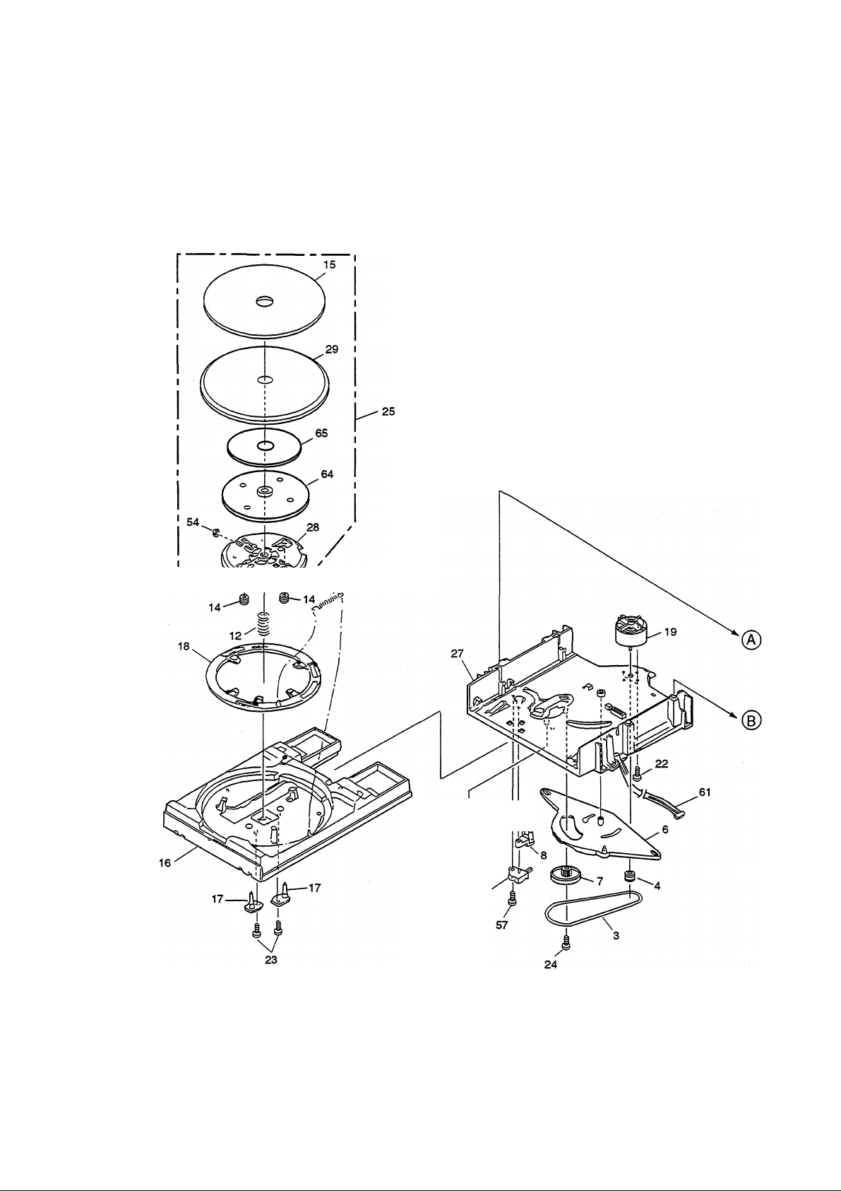
2. EXPLODED VIEWS AND PARTS LIST
NOTES: • Parts marked by ”NSP" are generally unavailable because they are not in our Master Spare Parts List
• The /1^ mark found on some component parts indicates the importance of the safety factor of the part.
Therefore, when replacing, be sure to use parts of identical designation.
• Screws adjacent to ▼ mark on the product are used for disassembly.
2.1 PACKING
Parts List
No. Description Part No.
Mark
Cord with Plug
1
Operating Instructions (English)
2
3 CD-R Disc Caution Card
Wireless Remote Control Unit
4
(CU-PD083)
Battery Cover AZA7123
NSP 6
5
Battery (R6P,AA)
Polyethylene Bag Z21-038
7
8 Mirror Mat
9 Styrol Protector F
PDR-04
PDE1248
PRB1251
PRM1046
PWW1116
VEM-013
Z23-007
PHA1243
NSP
10 Styrol Protector R
Packing Case
11
12
13 Warraty Card
PHA1245
PHG2223
ARY1044
Page 4
PDR-04
2.2 EXTERIOR
Page 5
PDR-04
Page 6

PDR-04
Parts List
Mark No. Description
NSP
NSP 2
NSP
NSP 4
NSP
A
A
A
A
A
NSP
NSP 21
NSP
NSP
NSP 31
NSP 32
STRATEGY SMALL BOARD ASSY
1
SERVO UCOM BOARD ASSY
3 AUDIO DIGITAL BOARD ASSY PWZ3388
ALC BOARD ASSY PWZ3389
5
HEADPHONE BOARD ASSY
e
O
7 FUNCTION BOARD ASSY PWZ3042
8 POWER A BOARD ASSY
9
POWER B BOARD ASSY
Strain Relief
10
39P F.F.C/30V
11
Connector Assy (5P) PF05PP-D37
12
AC Power Cord
13
Ferrite Core
14
Power Transformer
15
(Servo, AC120V)
Power Transformer
16
(Audio, AC120V)
17 Fuse(FU11,1A)
18 Screw
19 Cord Clamper
20 Cushion (3.5)
Spacer A
Rubber Spacer A
22
23
Rubber Spacer B
24 Under Base
25 Audio Angle
26 Rear Base
27 Earth Plate
28 Insulator
29 PCB Holder
30
PCB Holder
PCB Spacer
Loading Mechanism Assy TT
Headphone Knob PAC1600
33
Operation Button 78
34
35 REC Button
Part No.
PWX1518
PWZ3387
PWZ3390
PWZ3354
PWZ3359
CM-22C
PDD1181
PDG1015
PTH1018
PTT1308
PTT1309
REK1075
ABA1207
RNH-184
PEB1110
PEB1228
PEB1280
PEB1281
PNA2195
PNA2197
PNA2314
PBK1090
PNW1912
PNW2100
PNW2562
PNY-404
PXA1568
PAC1744
PAC1804
Mark No. Description
36
Power Button
Cord Clamper
NSP
37
38
Display Window
39
FL Sheet
40
Front Panel
41 Tray Panel
42 Display Panel 7
43
LED Lens
44 REC Ring
45 REC Lens
46
Holder
Tray Holder
47
48 Control Panel
49 Name Plate
50
65 Label
51
Indicator Lens
52
53
Bonnet
54 Screw
55
Ferrite Core
56 Screw
Screw
57
58 Screw
59
Screw
60 Screw
61 Rivet
Black Label
62
63 Screw
64 Disc Guard
65
Shield Sheet
66 1C
67 Earth Lead Unit
68 Binder Holder
Part No.
PAG 1805
DNF1128
PAM 1668
PAM 1673
PAN1349
PNW2701
PNW2662
PNW2019
PNW2558
PNW2559
PNW2591
PNW2592
PNW2703
VAM1032
ORW1069
PEA1206
PYY1175
BBT30P080FCC
PTH 1009
BBZ30P080FCC
IBZ30P060FCC
IBZ30P080FCC
IBZ30P150FCC
PPZ30P150FMC
RBM-003
PRW1470
FBT40P080FZK
PNM1245
PNM1308
PYY1196
PDF1154
PNW1021
Page 7
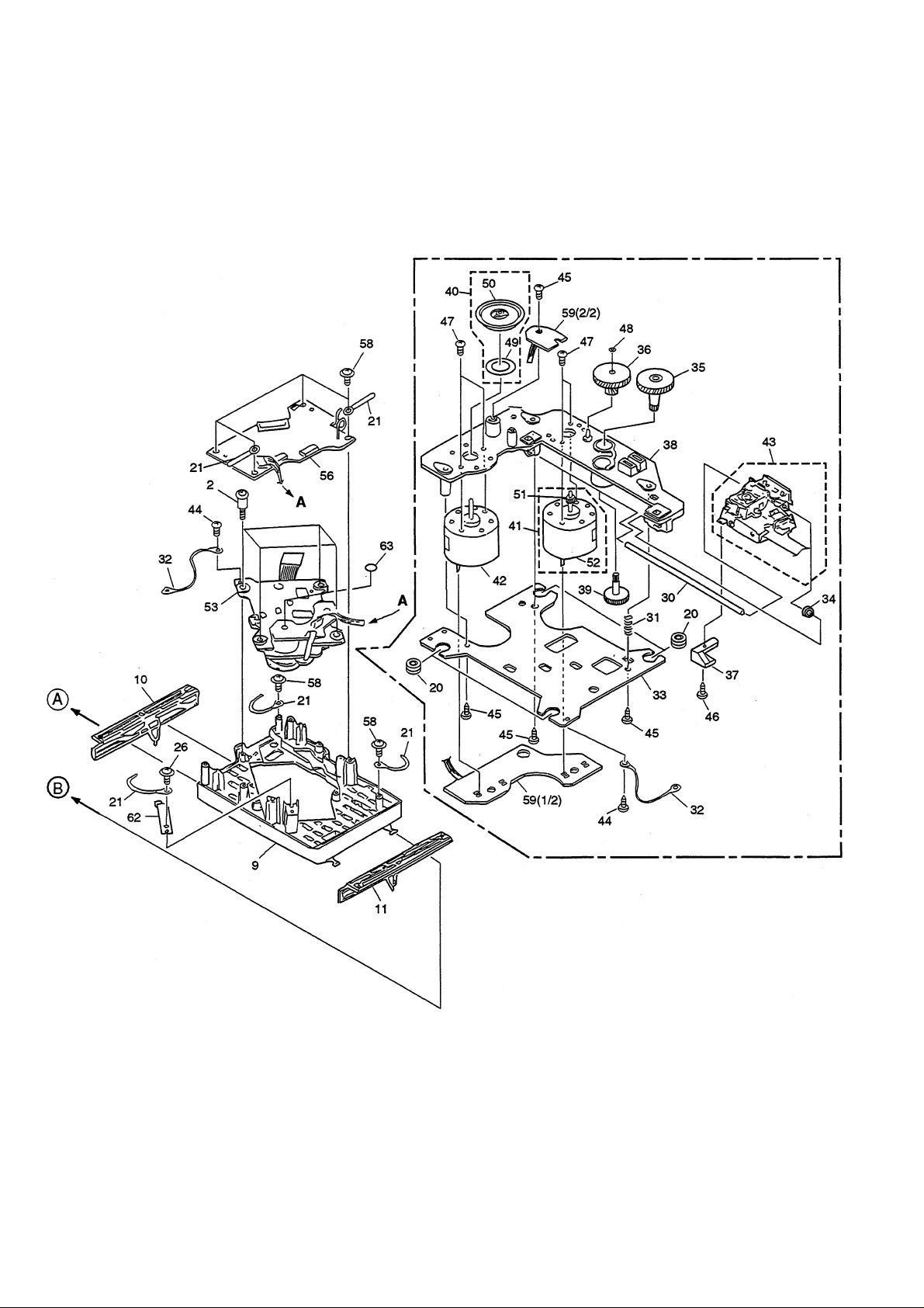
2.3 LOADING MECHANISM ASSY TT
PDR-04
13
Page 8
PDR-04
Page 9

Parts List
Mark No. Description
1 Lever Switch (Si 01)
2 Float Screw
3 Rubber Belt
4 Motor Pulley
5 Drive Gear
6 Timing Lever
7 Gear Pulley
8 SWHead
9 Float Base
10 Left Cam
11 Right Cam
12 Float Spring
13 Lock Spring
14 Float Rubber
15 Table Rubber Sheet
16 Tray
17 Table Guide
18 Lock Plate
19 D.C. Motor (0.75W,Loading)
20 Float Rubber
Part No.
DSK1003
PBA1027
PEB1186
PNW1634
PNW1996
PNW2168
PNW1998
PNW1999
PNW2563
PNW2001
PNW2002
PBH1120
PBH1121
PEB1014
PEB1181
PNW2003
PNW2004
PNW2005
PXM1010
PEB1031
PDR-04
Mark No.
NSP
NSP 53 Servo Mechanism Assy
NSP 56
NSP 59
NSP 64 Table Base Assy
NSP 65 Double Face Tape PNM1114
Description Part No.
51
Pinion Gear
52 Spindle D.C Motor (0.3W)
Stop Ring
54
55 Shaft Holder
HEAD BOARD ASSY
Screw
57
Screw
58
MECHANISM BOARD ASSY
60
61
Connector Assy 5P
62 Clamp Spring
63
Spacer PBF1014
PNW2515
PXM1033
PXA1560
YE20S
PNB1382
PWZ3386
BPZ26P060FMC
IB230P080FCC
PWZ3391
PDE1243
PBK1139
PXA1382
NSP
NSP
NSP
NSP
21 Cord Clamper
22 Screw
23 Screw
24 Screw
25 Turn Table Assy
26 Screw
27 Loading Base
28 Table Shaft Holder
29 Turn Table
30 Guide Shaft
31 Earth Spring
32 Earth Lead Unit /300V
33 TAN Base
34 Stopper Ring
35 Gear 2
36 Gear 3
37 TAN Plate TT
38 Mechanism Chassis
39 Gearl
40 Disc Table TT Assy
41 Carriage Motor Assy
42 D.C Motor Assy (Spindle)
43 Pickup Assy
44 Screw
45 Screw
46 Screw
47 Screw
48 Washer
49 Mirror Mat
50 Disc Table TT
RNH-184
BMZ26P040FMC
IPZ26P060FCU
IPZ20P080FMC
PEA1165
IPZ30P080FCU
PNW1995
PXA1383
PNR1035
DLA1530
PBH1196
PDF1088
PNB1514
PNM1246
PNW2513
PNW2514
PNW2518
PNW2520
PNW2521
PEA1323
PEA1324
PEA1325
PEA1341
BBZ26P040FMC
BBZ26P080FMC
BMZ20P040FMC
JFZ20P030FNI
WT12D032D025
PNM1247
PNW2516
•How to install the disc table
[T1 Use nippers or other tool to cut the two sections
marked ® in figure [I]. Then remove the spacer.
While supporting the spindle motor shaft with the
stopper, put the spacer on top of the mechanism chassis
and stick the disc table TT on top (takes about 9kg
pressure). Take off the spacer.
□
Mechanism _
Ch^is (A)
(Pressure of about 9kg)
Disc Table TT
^— 8.1mm
TAN base Stopper Mechanism Board
Page 10
PDR-04
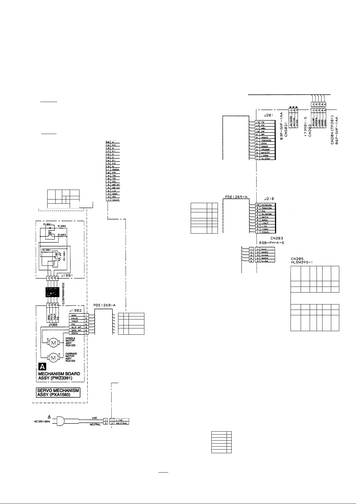
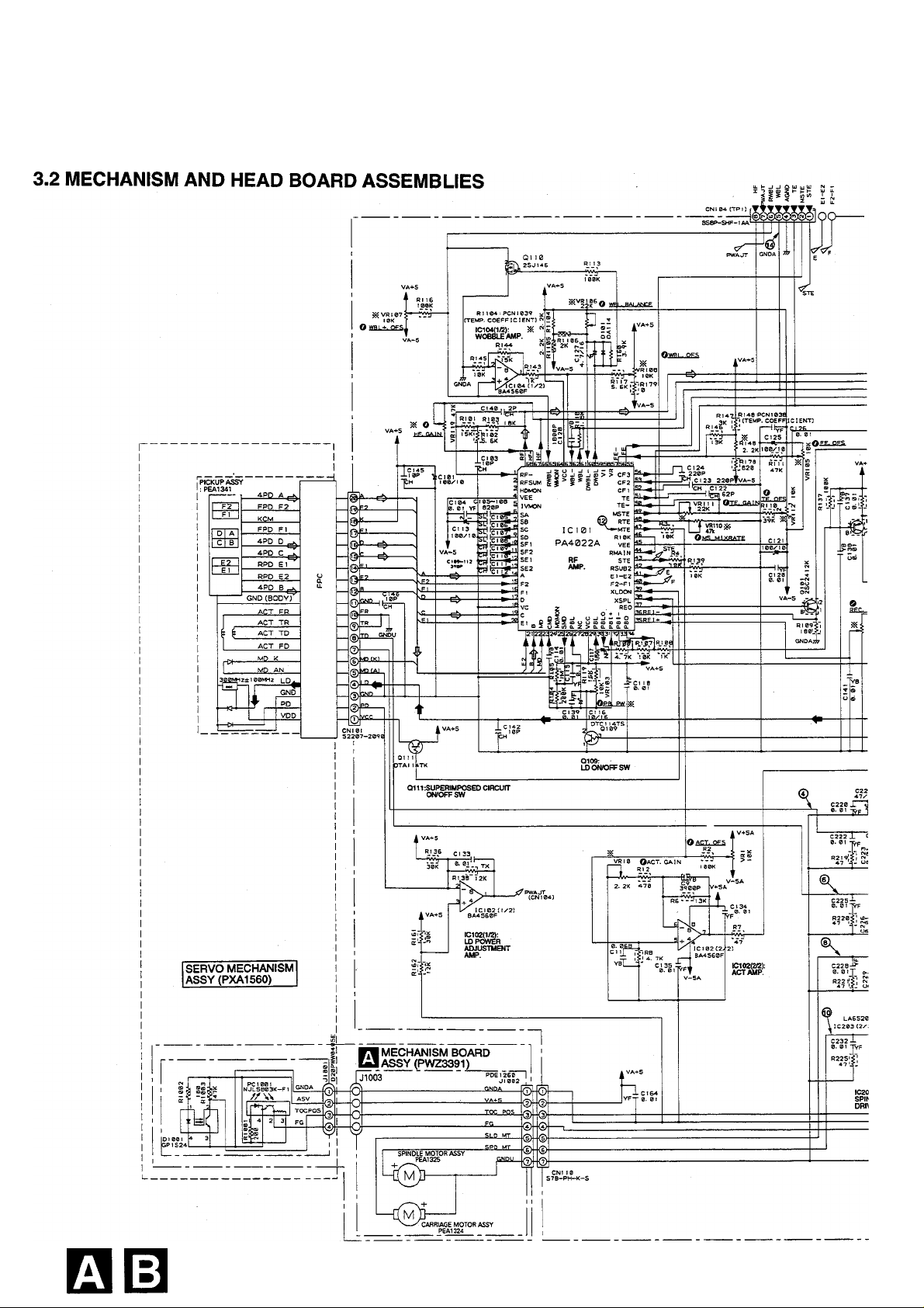
3. SCHEMATIC DIAGRAM
3.1 OVERALL WIRING DIAGRAM
S^01:DSIC1003
IPICKUPASSY]
I: PEA1341 I
D
■cTb;
: I , ACT TdI
I
------
-l_«c
J—
—KF
> Ar.T Pn
,.gNP
PD
-ypp-
CNI 01
52207-2090
CN 1 1 0
S7B-PH-K-S
GNDA
1 1
VA*S
7 7
4
FG
ff
SLD MT
fi
SPD MT
_z_
,»3NP.U
^ <
- <
s ^
Z 0-
o ®
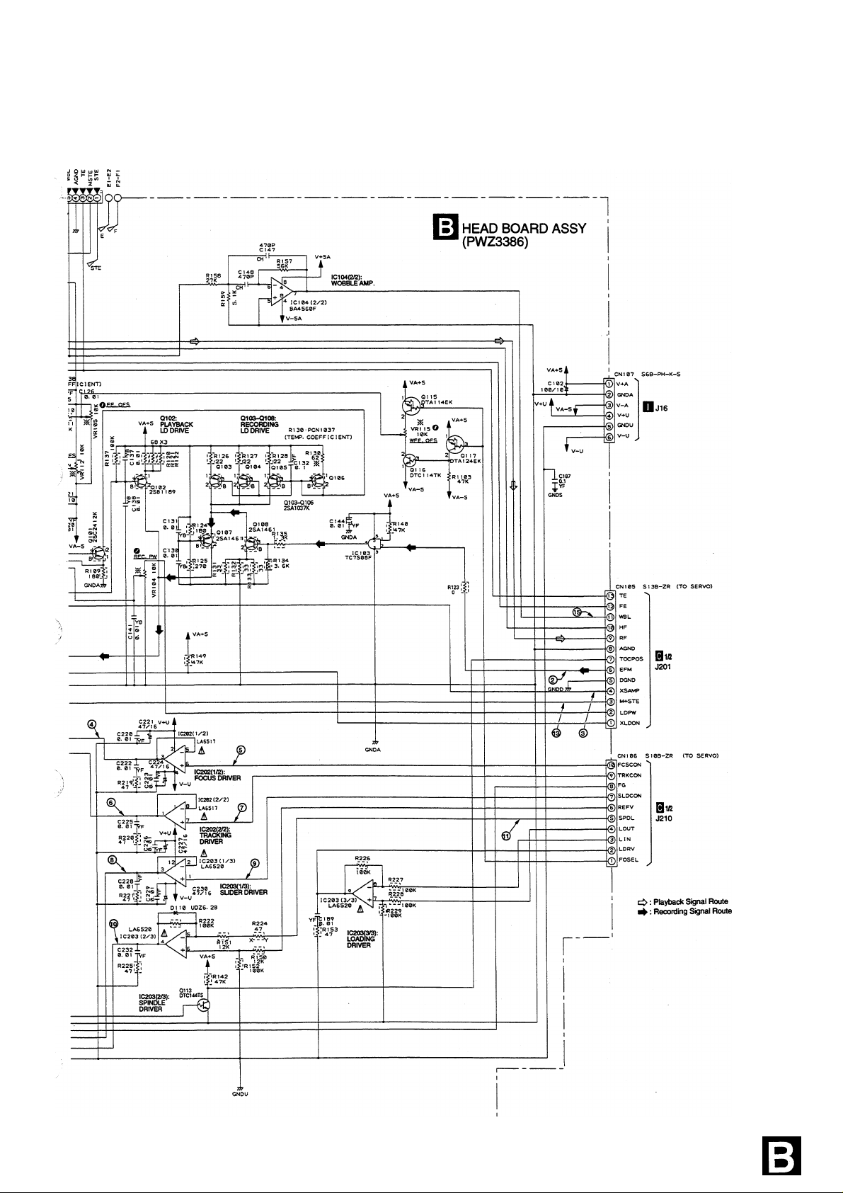
Is! HEAD BOARD ASSY
(PWZ3386)
S6B-PH-K-S
__
CNI 05
S13B-ZR
CNI 06
SI0B-ZR
TRKCQN
FG
RFFV
<;pnt
LOUT
1 IN 3
PQSgL
CN 1 07
.J
9
8 8
7
6 T
5 5
4
7 2
1
la.
9
4
3
PDE1264-A
tr □ (/;
L.
(/) Ij ^
S s| m ?i?|;r *r f
1 _ 11
1
T
- m
r‘
FUNCTION BOARD ASSY
(1/2) (PWZ3042)
^ in| U3r CO c
cl ^
K u3
tf) ujac
CN70I
HLEM39R-1
s tn r
1/) — ^
^ a
■
s - <
c ^ :
^ s ■
s - <
£ ^ :
s J
£ i
S si N i
1
1. 25mmP
T
- (N n -
s '
K ^ (0 1
IT J»
it in UJ
- I C
10
CN I I
RKC-061-0
DXWW0315E
CNI 2
B2P3-VH
m
POWER A BOARD ASSY
(PWZ3354)
[j904
PDEI273-A
J
V+AU
GAUD
V-AU
V4-5A
GNDA
V+5D
—QMPB
__
I
7
3
4
ft
fi
_2_
PF05PP-D37
PF06PG-D15
Q < 3 O
L_.
PF07PG-DI 0
Page 11
Note : When ordering service parts, be sure to refer to
"EXPLODED VIEWS AND PARTS LIST" or “PCB PARTS LIST"
HEADPHONE
BOARD ASSY
(PWZ3390)
PDR-04
B (l!]l/4,l!]2/4,l!]3/4,[!l4/4)
AUDIO DIGITAL BOARD ASSY
(PWZ3388)
11
Page 12
PDR-04
12
Page 13
PDR-04
13
Page 14
PDR-04
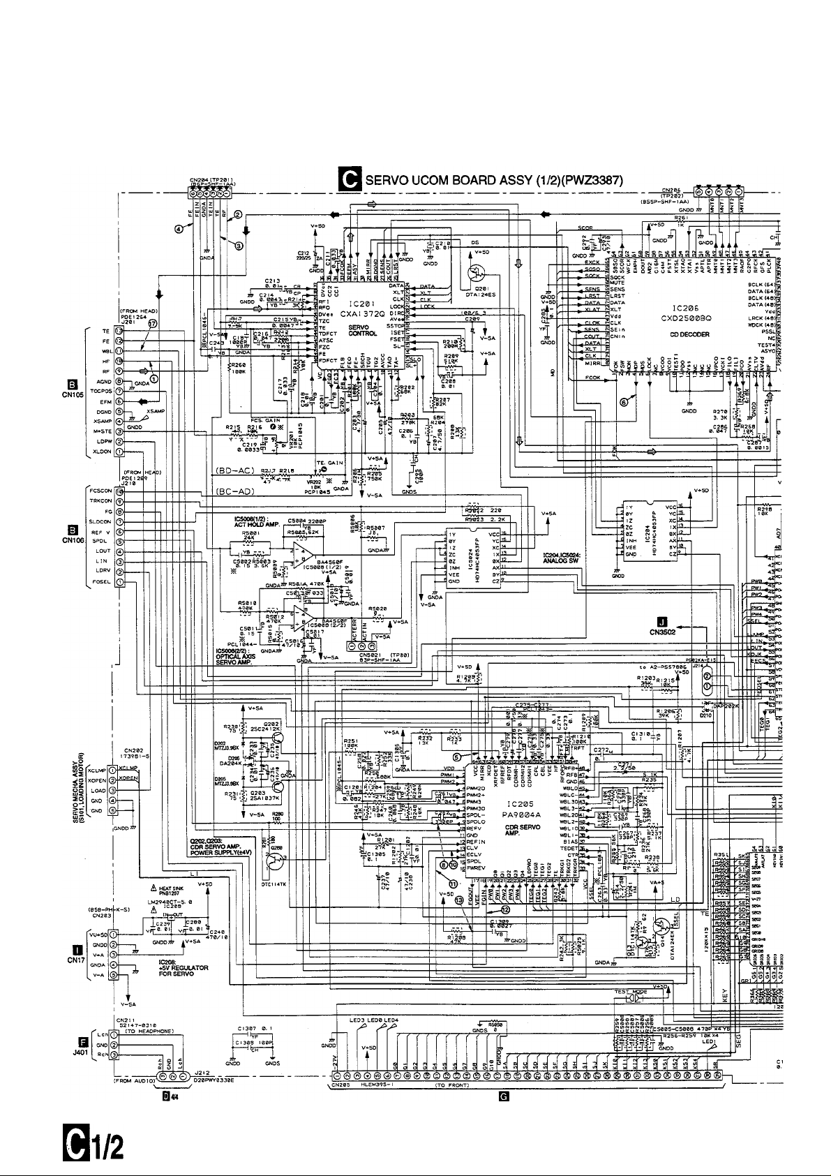
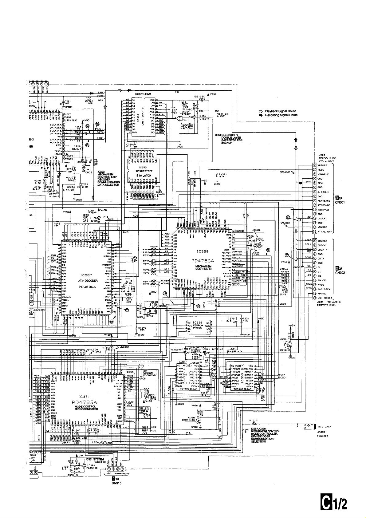
3.3 SERVO UCOM BOARD ASSY (1/2)
14
Page 15
PDR-04
15
Page 16
PDR-04
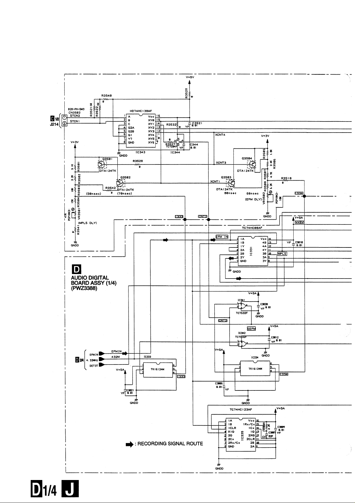
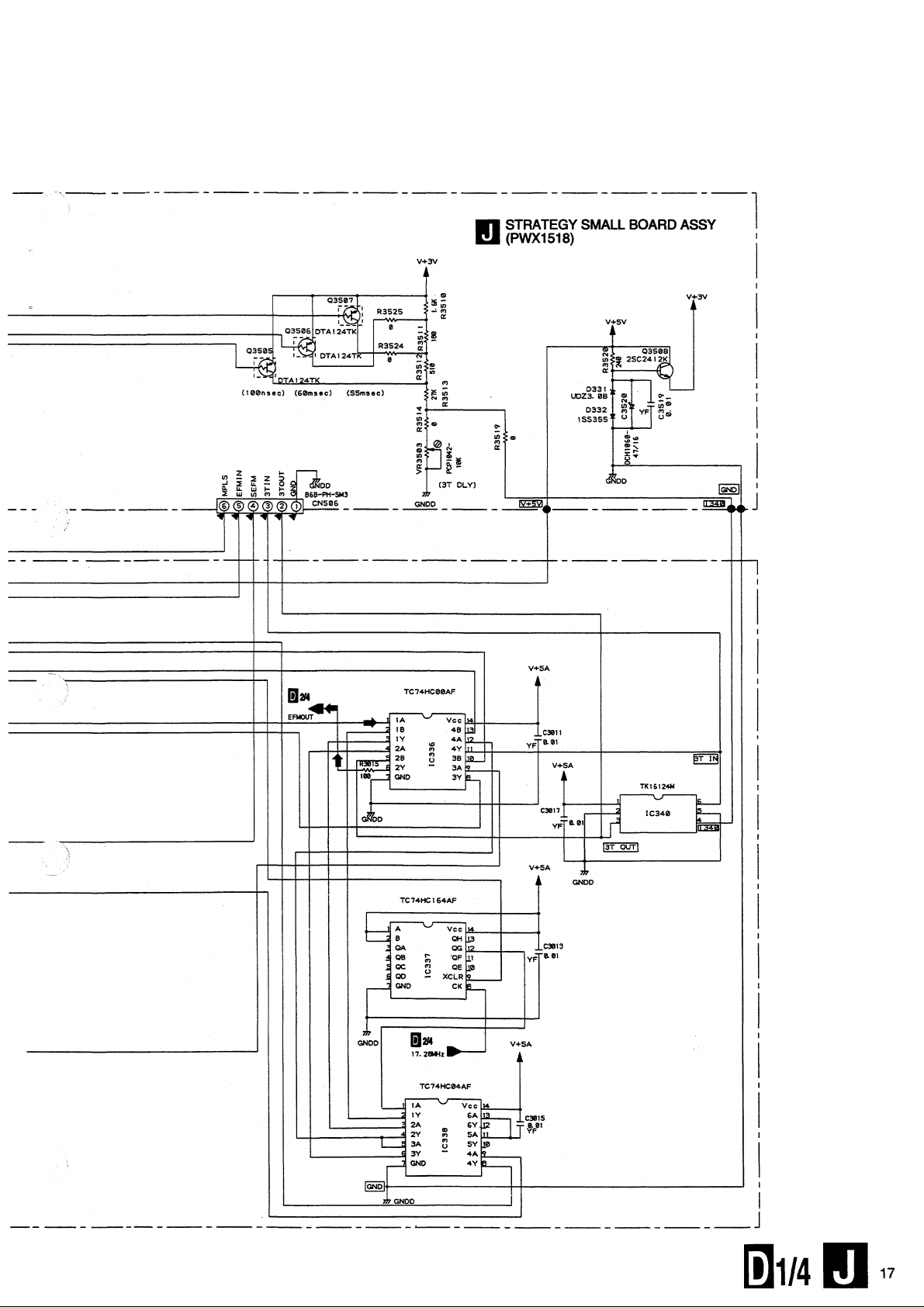
3.4 AUDIO DIGITAL BOARD ASSY (1/4) AND STRATEGY SMALL BOARD ASSY
16
Page 17
PDR-04
Page 18
PDR-04
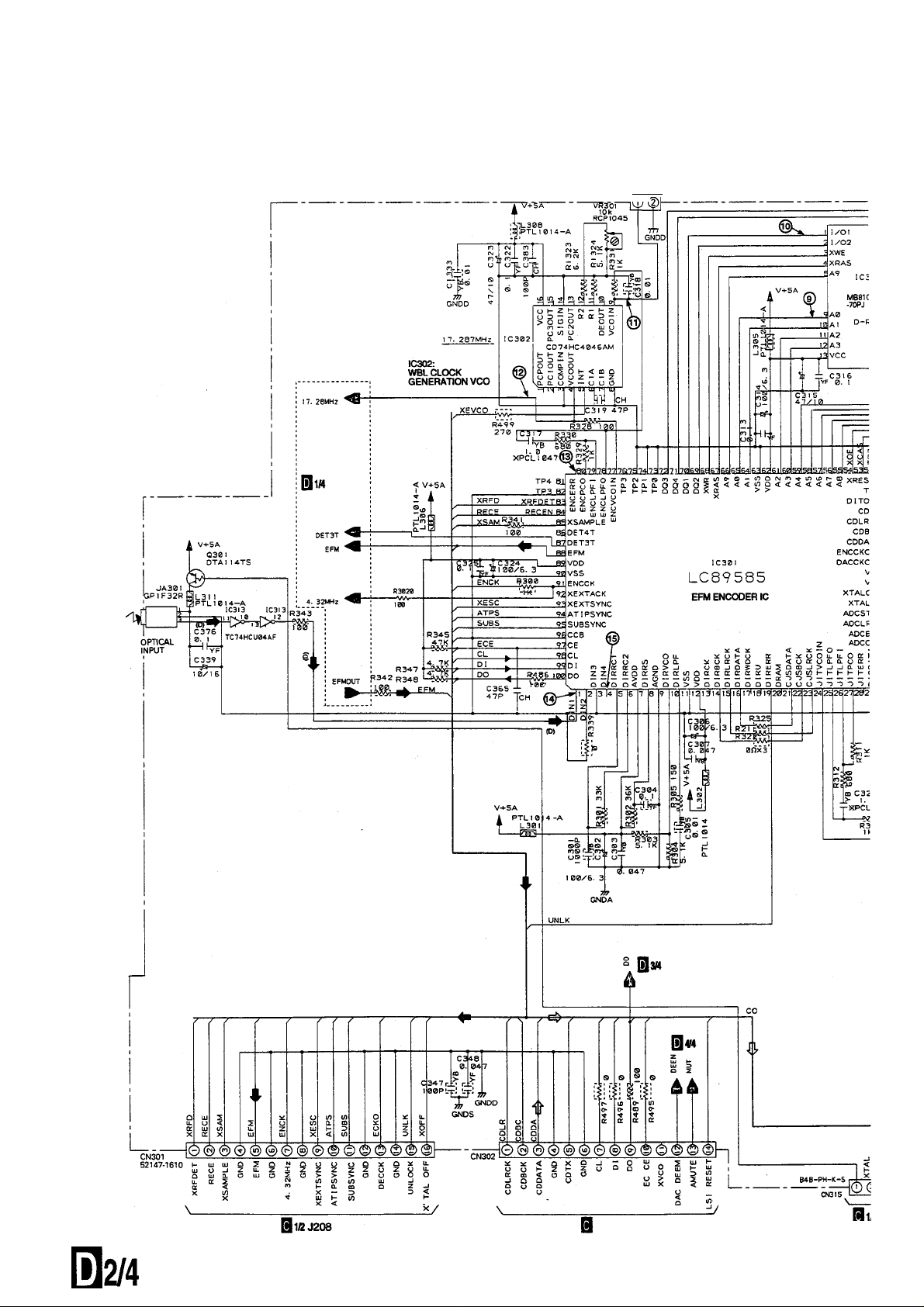
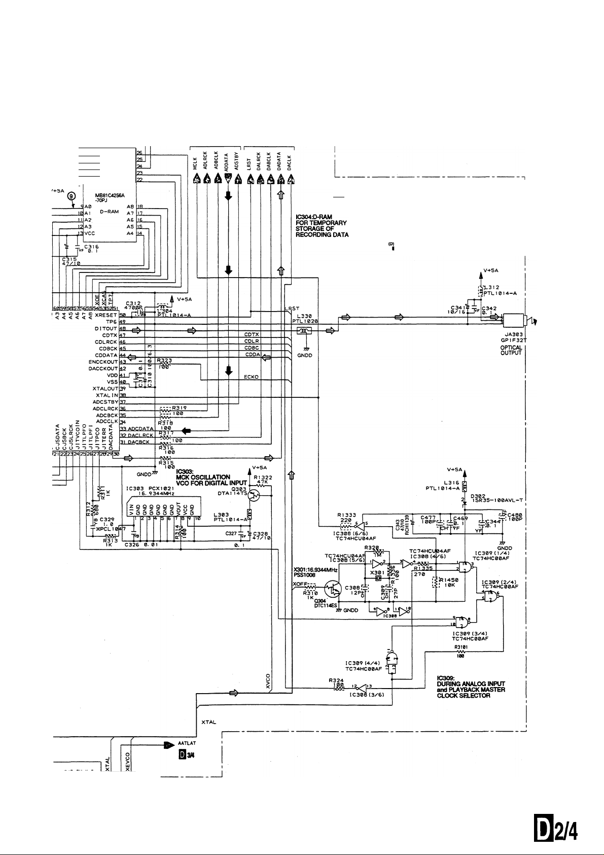
3.5 AUDIO DIGITAL BOARD ASSY (2/4)
CN331
B2P-SHF-1AA
18
1/2J209
Page 19
PDR-04
ll I/OI
d I/02
txwe
4XRAS XCAS
flA9
IC304
1/04
1/03
vss
fi1 AUDIO DIGITAL BOARD ASSY (2/4)
“ (PWZ3388)
c>: Playback Signal Route
1^: Recording Signal Route
: Recording Signal (Digital) Route
N
________
Qi/2J213
/
19
Page 20
PDR-04
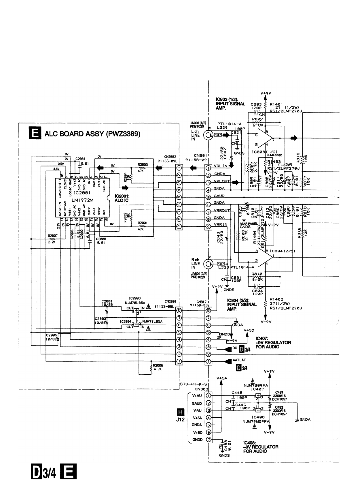
3.6 AUDIO DIGITAL BOARD ASSY (3/4) AND ALC BOARD ASSY
r—
20
Page 21
AUDIO DIGITAL BOARD ASSY (3/4)
(PWZ3388)
PDR-04
21
Page 22
PDR-04
3.7 AUDIO DIGITAL BOARD ASSY (4/4), SERVO UCOM BOARD ASSY (2/2) AND HEADPHONE BOARD ASSY
AUDIO DIGITAL BOARD ASSY (4/4)
(PWZ3388)
Q2/4
DALRCK I
DADATA I
DABCLK I
lrstI
R3IS 100
----------
VVV
---
_R3i^..l00_
R437
—wv
-----
C405:
RCH1139
Ю Ljf
if
100
IC40I
/
OKS
DVDD
DVSS
XTO
LL
>
XT I
1
1
XPD
04
BIOK
SDATA
LROK
SMUTE
DFS
DEM0 DEMI
IC401:
D/A CONVERTER
AOUTL
AOUTR
TLL
DZF
VREF
AVSS
AVDD
VOOM
BVDD
DIFl
DIF0
□
2Z.
22.
C408:
RCH1139
C406 C407
Ì
*1 0408
1 г 47/10
m
GAUD
0421
47/50
PCH1124
■—;й
- 0422
в 47/50
POR1124
--
---
[=>: Playback Signal Route
П
0401.0402:
INVERTER BUFFER
22
Page 23
PDR-04
SERVO UCOM
BOARD ASSY (2/2)
(PWZ3387)
HEADPHONE BOARD ASSY
(PWZ3390)
2/2 014/4
23
Page 24
PDR-04
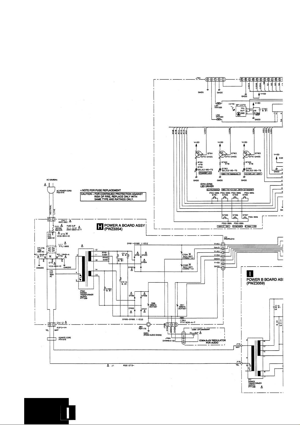
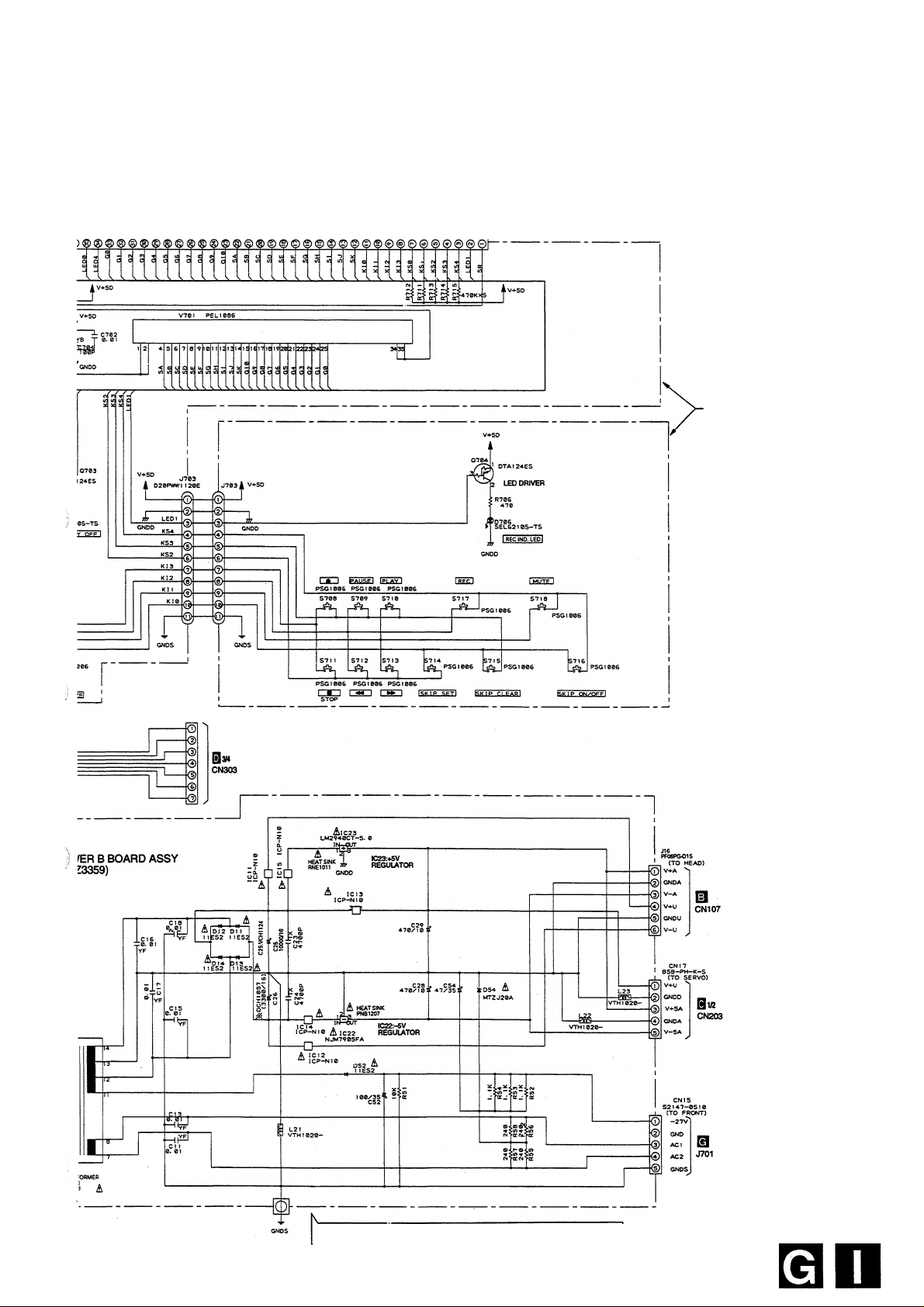
3.8 FUNCTION, POWER A AND POWER B BOARD ASSEMBLIES
D20PWY05ISE « <
24
GlH
Page 25
CN70I HLEM-39R-1 (FROM SERVO)
PDR-04
FUNCTION BOARD ASSY
(PWZ3042)
• SWITCHES
S701 : AUTO/MANUAL
S702: WRITE
S703: DISPLAY OFF
S704: STANDBY/ON
S705: INPUT SELECTOR
S706: DIGITAL SYNCHRO
S707: FINALIZE
S708: ± (OPEN/CLOSE)
S709: II (PAUSE)
S710: ► (PLAY)
5711 : ■ (STOP)
5712 (TRACK/MANUAL REV)
5713 : (TRACK/MANUAL FWD)
S714: SKIP SET 1 gKIP ID
5715 : SKIP CLEAR ^
5716 : SKIP PLAY ON/OFF
S717:#(REC)
S718 : O (REC MUTE)
CAUTION - FOR CONTINUED PROTECTION AGAINST RISK OF FIRE. REPLACE ONLY
WITH SAME TYPE No. ICP-N10, MFD BY ROHM CO.. LTD. FOR IC11 - IC15.
25
Page 26
PDR-04
3.9 WAVEFORMS AND VOLTAGES
HEAD BOARD ASSY
• Waveforms and voltages of HEAD BOARD ASSY
• Measuring condition : DC input unless othenwise noted.
CN105 pin 6 (EFM)
©
CN105 pin 4 (XSAMP)
©
Test mode
During maximum recording
power laser diode ON
2V/div 0.2pS/div
(t ) IC202pin7(TRKCON)
^ 2V/div 0.5mS/div
6) IC202pin1 (TD)
0.2V/div 0.5mS/div
During PLAY
©
®nn
©I
IC202 pin 6 (PCS ON)
(4) IC202 pin 3 (FD)
During PLAY
SV/div ImS/div
©
-GND
(9) IC203pin 1 (SLDCON)
(i) IC203 pin 3 (SLD MT)
During PLAY
O.SV/div 0.2mS/div
©
©
©
IC101 (PA4022A) [ V
Pin
No.
1 0.01 2
3 0
4
5 0
6 0
7 0 0 0 41 0
8
9 0
10 0
11 0
12 0
13 0 0 0 47 0 0
14 0
15 0
16 0
17 0
18
19 0
20 0
21
22 0 0 0 56 0 0
23 1.4
24
25 0 0 0.9 59 -2.9
26 0
27 0
28
29 5.0
30 4.2
31 -3.4 -1.7 -1.7 65 0 -0.1 0
32 0 0 0 66
33 -1.0 0 0 67
34 4.3
MODE
STOP
PLAY REC
0.02 -0.12 -0.4 36
-0.16 0
-4.9 -4.9 -4.9 38 0.1 0.1
0 0
0
0
0 0 42
0 0 43
0 0
0 0
0 0
0 0 48
0 0
0 0 0
0
0 0 52 0 -0.1 0
0 0 S3
0 0 54
0
0 0
1.4
1.4
1.4 1.4 58 -4.0
0.2
0 ^2
0
0 0 62
5.0 5.0
1.2 1.2
3.6
-GND
©
-GND
Pin
No.
-0.1 35
37
39 5.0 0
0 40 0
44 0
45 -4.9 -4.9
46 0 -0.1
49 0 0
50 0 0
51 0 0
55 0 0
1.4. 57 0.1 0.1
02 60
61 0 0
63 5.0 5.0
64 -0.1
3.6 68 -0.1
MODE
STOP
0.6 0.6
0.6 0.6
1.2 1.2 1.5
0 0
0 0
0 0
0
0
0 0
0 0
-0.3 1.4
0 0
PLAY
0
0
-0.1 -0.1
-0.1
0.2
■4.0
-2.7
0.3
0
REC
0.8
0.8
3.1
-0.1
0.1
-4.9
-0.1
-0.1
0.2
0.1
-4.0
-2.7
5.0
0.3
1.2
CN106 pin 5 (SPDL)
1V/div 2mS/div
(10) IC203pin4(SPDMT)
^ 2V/div 2mS/div
During PLAY
©-
GND
-GND
IC101 pin 47 (MTE)
200mV/div
CN105 pin 3 (M+STE)
@
500mV/div
@ TP1 pin 5 (WBL)
@ CNIOSpinll (WBL)
-GND
(is)-/V/V/V/V/i»-GND
-GND
During CD-R PLAY
lOOmV/div 20pS/div
Test mode
'^°'spdl)'^'-ose
-GND
-GND
0
IC102(BA4560F)[V]
Pin
No.
1
2
3 4.4 1.4
0
0
0
4 -5.0 -5.0 -5.0
5
6 0 0 0
7 0 0
8
MODE
STOP PLAY REC
0
0.2 1.5
1.4 1.4
0 0
5
0.1 to
5 5
1.5
1.4
0.6
0
IC103 (TC7S08F) [ V
Pin
0
0
0
0
0
0
0
0
0
0
0
0
No.
1
2
3
4
5 5 - -
IC104(BA4560F)[V]
Pin
No.
1
2 0 -0.1 -0.1
3 0
4
5
6 0 0 0
7 0 0
8
MODE
STOP PLAY
0 0
0 0 2.0
- -
0
0
0 2.0
MODE
STOP PLAY
0 -0.1
-0.1
_
-5.0
0 0 • 0
5.0
- -
REC
0
REC
-0.2
-0.1
-
C
TRK OPEN
-GND
-GND
IC202(LA6517)[V]
STOP
0
9.4
-0.4
0 0
MODE
PLAY REC
0 0
- -
-0.4 -0.4
-
Pin
No.
1
2
3
4 -10.0
5 -0.4 -0.4
6 -0.4 -0.4 -0.4
7
8 0 0 0
IC203(LA6520)[V]
Pin
No.
1 0.01 0.01
2 0.01 0.3
3 0 0.3
4 0.04 -0.1
5 Z2 2.2 2.2
6 2.2 Z2 2.2
7 0 0
8 0 0
9 0 0
10
11 12
FIN -10.0
MODE
STOP PLAY REC
-
-
-
-
9.4
-
-
-0.4
0
Oto
0.2
0.1 to
0.4
0.2 to
0.3
-0.5 to
-0.7
0
0
0
-
-
-
-
Q101 (2SC2412K) [V]
Pin
No.
E 0.6
C
B 12 1.2
MODE
STOP PLAY REC
0.6
0.8
-
-
1.4
Q102(2SB1189)[V]
Pin
No.
E
C 1.5
B 42
MODE
STOP PLAY
5.0
5.0
1.5 1.8
3.8
REC
4.5
3.8
Q103(2SA1037K)[V]
STOP
5.0 5.0
1.0 1.0
-
MODE
PLAY REC
4.8
2.2
- -
Pin
No.
E
C
B
26
Page 27
PDR-04
Q104(2SA1037K)[V] Q106 (2SA1037K) [ V] Q109 (DTC114TS) [ V]
Pin
No.
E 5.0 5.0
C 1.0 1.0
B
MODE
STOP PLAY RED
4.8
2.2
- -
-
Pin
No.
E
c
B
Q105(2SA1037K)[V] Q107 (2SA1461) [ V]
STOP
- -
MODE
PLAY
1.0 2.2
REC
-
Pin
No.
E
c
B
Pin
No.
E 5.0 5.0 4.8
C 1.0
B
MODE
PLAY
STOP
5.0 5.0 4.8
- - -
- -
-
MODE
PLAY
STOP
- - -
1.5 1.5 1.8
3.0 3.0 3.0
REC
REC
Pin
No.
E 0
C 0 1.1
B
MODE
STOP PLAY
-
5.0 0
REC
-
1.2
0
Q111 (DTA114TK)[V]
Pin
No.
E 5.0
C
B 5.0 0 0
MODE
PLAY
STOP
- -
0 0 4.4
REC
SERVO UCOM BOARD ASSY
I Waveforms and voltages of SERVO UCOM BOARD ASSY
> Measuring condition : DC input unless otherwise noted.
J201 pin 10 (HF)
@ CN204 pin 1 (RF)
During CD PUY
SOOmV/div 0.5pS/div
@ 1C205 pin 63 (MIRR) 2V/div
@ CN204 pin 1 (RF) 0.5V/div
During manual search
0.5mS/div
©I
-GND
-GND
IC356pin48(SPSP)2V/div
@ IC205 pin 13 (CLV) lOV/div
IC205 pin 14 (ECLV) 10V/div|
In the /FCSON
test mod(
test mode SPDLON (CD)
20fiS/div
®
------------
®==
TRK OPEN
(?) J201 pin 10 (HF)
©1
GND
0
■GND
(2Ò)
•GND
IC356pin23(RFT)
@) IC356pin24(RFB)
During CD-R PLAY
(in common with GND of ® and
IV/div ImS/div
-GND
-GND
CN204 pin 2 (TE)
(D
Test mode
TRK, CLOSE state
Top : FILTER exist
Bottom; FILTER none
SOOmV/div 0.5mS/div
CN204 pin 2 (TE)
©
Test mode/FSC, SPDLON
Top ; FILTER%xist
Bottom: FILTER none
SOOmV/div 0.5mS/div
CN204 pin 6 (FE)
©
Test mode
TRK, CLOSE state
0.5V/div 2mS/div
I TRK, OPEN
@ IC206pin4(MDP)2V/div
@ IC205 pin 13 (CLV) lOV/div
@ IC205 pin 14 (ECLV) lOV/div
During CD PLAY
20pS/div
©
-GND
-GND
IC207 pin 4 (MDP) 2V/div
@ IC205 pin 13 (CLV) lOV/div
IC205 pin 14 (ECLV) lOV/div
During CD-R RE
20pSMiv
-GND
® '
...........
-GND
®
@ IC205 pin 13 (CLV) lOV/div
@ IC205 pin 14 (ECLV) lOV/div
....
--------------
IC205 pin 9 (SPDLO) IV/div
During STOP
20pSraiv
@ IC205pin19(FGIN)
@ IC205 pin 17 (FGOUT)
In the test mode
/FCSON
SPDLON (CD)
\TRK OPEN
2V/div 2mS/div
©ruuuuinr.
-GND
-GND
-GND
©jiniuinri-
IC206pin34(DATA)
@ IC206pin32(LRCK)
@ IC206pin35(BCLK)
During CD PLAY (1kHz OdB)
lOV/div 2pS/div
-GND
=
0
-GND
0
-GND
@ J201 pin 11 (WBL) 50mV/div
@ IC207 pin 1 (WBL) 2V/div
During CD-R PLAY
20nS/div
-GND
-GND
-GND
-GND
@ J209 pin 5 (DOUT) 5V/div
J208 pin 13 (MCK) 2V/div
During CD PLAY
O.lpS/div
-GND
-GND
-GND
©■
®.
©y\AAA/- GND
-GND
-GND
-GND
27
Page 28
PDR-04
IC201 (CXA1372Q) [V]
Pin
No.
1 0 0
2 0 0
3 0 0
4
5 -0.4 -0.4
6 0 0
7
e 0
9 0 0
10
11
12 0 0
13 0
14 0 0.3
15
16 -4.0 -4.0 -4.0
17
18 0 0
19 -4.0 -4.9
20
21 5.0 5.0
22 4.8 4.9
23 5.0 5.0
24 0.7 0.7
MODE
STOP PLAY
0 0
0.3 0.3
0
5.0 5.0
0 0
0
0
0
1.3 1.3
5.0
5.0
Pin
No.
REC STOP PLAY REC
0 25 4.9
0
26
0 27 0.8 1.5 1.9
0 28
-0.4
29
0 30 -4.9
0.3 31 2.5
0
32
0 33 0.1 5.0 5.0
5.0 34 1.4
0 35 -1.0 -1.4
0 36
0 37 0 -0.4 -4.0
0.3
38 -4.0 -3.2 -1.9
0 39 0 0 0
40 -0.1 0.1 3.9
1.3 41 -4.9 -4.9 -4.9
0
42
-4.9
43 0 0 0
5.0 44 0 0 0
5.0 45 0 0 0
5.0 46 0 0 0
5.0 47
0.7 48
MODE
4.9
0.1
0.1 1.2
0
0 0
0
0 3.7
-4.9 -4.9
2.5 2.5
2.6 2.6 2.8
-1.1 -4.8
5.0
5.0 5.0
0
0 0
0 0
0.2
0 0
0.2
IC207 (PDJ006A) [ V
STOP
0.1 2.3
5.0 5.0
0
0.3
0
2.4
0
0.1 0.1
3.3
3.2
1.2
MODE
PLAY
0
0
0
Pin
No.
REC
41 4.9
2.1
2.8 42 5.0 5.0
0.1 43 5.0 5.0 5.0
2.S 44 5.0 5.0 5.0
45 0
0
0.2 46
47 0 0 0
0
0
48
5.0 49 0 0 0
02 50
5.0 51
5.0 52
0
5.0
2.4
3.3
3.2
1.4
53 0 0 0.
2A
4.9
54
5.0 55
5.0 56 0 0 0
5.0
57
5.0 58 5.0 5.0
59 1.9
04
-
60 5.0
4.9 61
4.9 62
1.3 63
2.2 64
65 5.0 0 0
22
67 5.0 5.0 5.0
1.1
0 68
1.7 69
0.8 70 5.0 0 0
4,7 71 0 5.0 5.0
3,1 72
73 0 0 0
3.3
2.8 74
2.9 75
2.5 76
3.4 77
5.0 78
1JS 79
80 0 0 0
3.3
Pin
No.
1
2 5.0 0
3 0.1 0
4
5
6
7
8 0 0
9 5.0 5.0
10 0.1 0.1
11 5.0 5.0
12 5.0 5.0
13
14 4.9 4.9
15 0 0
16 0 0
17
18 5.0 5.0
19
20 4.9 4.9
21 4.9 4.9
22 4.9 4.9
23 1.6 0.9
24
25 3.6
26 4.1 3.2 3.5 66 5.0 5.0 5.0
27 1.1 0.9
28 0 0
29 1.4 1.0
30 0.5 0.7
31 4.7 4.7
32 2.8 3.4
33 3.0 3.1
34
35 3.2 3.4
36 1.8 1.8
37 3.4 3.2
38 5.0 5.0
39
40 2.9 2.6
MODE
STOP PLAY REC
5.0
0
0
0
0 0 0
0
0 0
0 0
0
0 0
0
0
0
0 0
0
0
1.6
5.0
0
0
0
0 0
0
5.0
0 5.0 0
0
0 0
5.0
0 5.0
0 0 0
0
0
0 0 0
0 0 0
0
0
5.0 5.0 5.0
0 0 0
IC205(PA9004A)[V
Pin
No.
0
1
2
3 3.1
4
5
6
7
8
9
-4.8
10
11 0
12
13 0
14 0
15
16 0
17
18
19 0
20
21 0
22 0 0 5.0
23 0
24 0 0
25
26
27
28 0
29 0
30 0
31 0
32 0
4.9
5.0
0
0
IC208 (LM2940CT-5.0) [ V ]
Pin
No.
0
IC311 (PST529C)[V
0
No.
0
5.0
2.5
5.0
0
IC204 (HD74HC4053FP) [V]
5.0
No.
0
0
MODE
STOP PLAY REC
5.0 5.0 5.0
2.5 2.4 2.5 34
3.1 2.5
0.8 0.8
0.8 0.8 2.3 37 0 0 0
2.5 2.5
2.5
2.5 2.4 1.8
2.5 2.5 2.5 40 0
2.4
2.6
2.5 2.5 2.5
0
2.4 2.4 24 44 0
4.9 4.9
4.9
2.5
2.5
0 0 48 1.6
5.0 2.8 2.8 49 1.6
-4.0 -4.0 -4.0 50 1.6
3.3 3.3 51
0
0 0 52 -0.3 1.4 1.8
0 0 53 -4.0
0 5.0 55 -1.0 1.5 1.3
1.0 1.0 57 0 0 0
5.0 5.0
0
5.0 0 59 0 0.9 0.3
0 0 60 0.4 0.4 0.4
0 0
0
0 0 63
0 0 64 3.9 3.9 3,9
MODE
STOP PLAY REC
U
G
Pin
1
2 0 0 0
3
Pin
1
2 0 0 0
3
4
5
6
7
B
9
10
11
12 5.0 5.0 5.0
13
14
15
16
- -
9.3
-
0
5.0
- -
MODE
STOP PLAY REC
5.0 5.0 5.0
5.0 5.0 5.0
MODE
PLAY REC
STOP
0 0 0
0.9 1.5 1.9
0.1 9
0.9
0.1
0.1
0 0
0
0 0
0
0 0
0
5.0 0
0 0 0
0 4.9 0.2
0 5.0
5.0 5.0 5.0
0 0 0
5.0 5.0
Pin
No.
STOP PLAY
3.9
33
0 0 0
35 0.6 0.6 0.6
2.3
36
0.1 0.1
38 0 0 0
0
39
41 0
ZJS
0 43
0 46 0 0 0
2.6 47 1.6
0 56 -0.3 1,9 1.9
5.0
0 62
-
1.3
0
42
0
5,0
45
1.6 1.6 1.6
54 0.3 1.4 2.3
58 -0.8
5.0
61
1.7
5.0
s.o
5.0
S.O
MODE
3.9 3.9
0 0
0 0
0 0
0 0
0 0
0 0
2.4 2.4
0.9 1.2
2.6 1.2
2.6
2.6
-4.0
-0.6
0 5.0
0.4 1.7
5.0 2.8
IC206 (CXD2500BQ)
Pin
No.
REC
0.1
1.9
1.9
-4.0
-0.8
1 0.1 4.9
2 0
3 0 5.0 5.0
4 2.4 2.5 3.8
5
6
7 0.1
8 S.O S.O 5.0
9 0 0 0 49 0
10 0 0 0
11 0.1 0.2
12 0 0 0
13 0.1
14 0.1
15 0.1
16 5.0 5.0 5.0
17
18
19 2.5
20 2.5 2.5 2.5 60
21
22 2.6 2.6 2.6
23 5.0 5.0 5.0
24
25
26 0 0
27 2.5 2.5 2.5 67
28 0
29 0 0,1 0.4 69 0.1
30 0 0 0 70 4.9
31 2.5 2.5 2.5 71 0.7
32 0
33 5.0 5.0 5.0 73 5.0
34 0 1.2 0 74 4.8
35 1.9 1.9 1.9 75 0.9
36 0 1.2 0 76 0.8
37 1.9 1.9 1.9 77 0.7
38 2.5 2.5
39 5.0 0 0 79 4.8
40 5.0 5.0 5.0 80 0.9
MODE
STOP PLAY REC
0.2 0.6 42
0.1 0.2
S.O 5.0
0
0.2
0.2
0.2
0.2
0
0
2.6
2.6
2.5
0 0
2.6 2.8
2.6
0.1 0.4
0
0
0.1 2.5
V]
Pin
No.
STOP
41 1.1
4.8
43
44 S.O
0.6
45
46 4.3
0.6 47
48
50 1.2
0.6 51
52
0.6
53 2.1
0.6 54
0.3
55
56 2.8
0 57 1.0
2.6 58
2.5 59 5.0
0 61
62
63
64
65
0 66
0 68
72
78 5.0
2S
MODE
PLAY REC
0
2.5
0
3.3
3.3
1.2
0
2.8
0
2.1 2.1
2.1
0
2.5
0
1.5
0
0
4.9
0
4.9
1.1 1.1
5.0 5.0
2.5 2.5
0 0
5.0 5
4.4 4.4
0 0
0 0
0 0
1.2 1.2
1.2 1.2
0
2.1 2.1
2.7 2.7
0 0
2.7 2.7
1.0 1.0
5.0
2.1 2.1
0
2.5 2.5
0.1 0.1
0.1
0
4.6
4.9
0
2.7 2.8
4.9 4.9
0.6
4.9
5.0
4.9 4.9
1.4
0.1 1.7
0.6
5.0 5.0
4.9 4.9
0.1 1.8
IC352(LH5116NA-10)[V] IC353 (HD74HC573FP) [ V]
Pin
No.
STOP
1 2.8
0.7
2
3 3.8
4 2.7
5 4.0
6 3.6
7
3.2 2.5 2.6
1.5
8
9 2.7
10 3.0
11 3.2
0
12
3.3
13
1.8
14
3.4
15
16 1.2
2.9
17
18 4.5
19 0.9
4.9
20
21 4.9
22 2.7
23 2.8
4.6
24
MODE
PLAY REC
2.7 2.7
1.4 1.1
3.7
3.3
2.0 2.5
3.4 3.7
3.0 2.6
0.9 1.1
3.3 3.1
3.3
3.1
3.0
3.1
0 0
3.4 3.2
2.0
1.8
3.4
3.3
1.5
2.8
2.7
4.5
4.5
0.8 1.1
4.9
4.9
4.9
4.9
2.5
2.5
2.9
2.8
4.5
4.6
Pin
No.
1
2
3 3.0 3.2
4 3.2 3.2 3.0
5 3.2
6
7
8 1.2
9
10 0
11 0.1 0.1
12 2.8
13 0.8
14
1.4
15 0.3 1.9
16
17
18 3.2
19 1.5 0.9
20 5.0
STOP
0 0
2,7
1.9
3.5
2.8 2.7
3.9 3.5
4.1 3.0
3.6
MODE
PUY
3.4
3.3
1.8
3.1
1.4
0
2.7
1.6
3.2 Z2
2.3
5,0
REC
0
3.1
3.4
3.2
2.1
3.3
1.4
2.7
0
0.1
3.0
1.0
3.7
2.9
3.4
Z2
1.4
5.0
0
2.1
5.0
0
0.1
0
4.7
4.9
0
0.7
4.9
5.0
1.7
0.7
28
Page 29
PDR-04
IC351 (PD4785A) [ V
Pin
No.
1
2 0 0 0
3 0 0 0 43 0
4 0 0 -22.0 44 0.1
5 -22.6 0 -22.0 45 5.0 0 0.1
6 0 -22.0 -22.0 46 0.08 0 0.1
7 -22.6
8
9 0.06
10 0.06 0 0 or 5 50
11 0 0 0 51 4.9 4.9 0
12
13 5.0
14
15 4.5 0 0 55
16 0.8 0 0 56 -23.6 -23.2
17 5.0 0 0 57 -23.6
18
19 0.08 0 0 59
20 0.08 0 0 60 0 0 0
21 0.08 0 0 61
22 0.05 0 0 62
23
24 0
25 5.0
26 0.06 5.0
27 5.0 5.0 67 -21.8
28
29 0.06 0 0.1 69 -24.6
30 0.06 0 0.1 70 -8.8
31 0 0 0.1 71
32 0.07
33 0.07 0 0.1 73
34
35 0.06
36 0
37 0.06 0 0.1
38 0
39
40
MODE
PLAY
STOP
-22.0 -22.0 41 4.8 4.8
-22.6
-22.0
5.0 5.0 5.0 48 0.07 0 0.1
5.0
5.0 5.0
5.0 0
5.0 0 0 54
5.0 5.0 0 58 0 0
5.0 5.0 63 4.6 4.6
0 0
5.0
0 0 0.1
0
0.07 0 0.1 74 -9.6
0
0
0 0 78 -22.4 -22.1 -22.0
0 0 79 -22.3
4.9
0.05
Pin
No.
REC
42
-22.0 47 0.08 0 0.1
5.0 49
52
53
64 0 5.0
5.0 65 -24.6
-
66 -13.8
68
0.1 72 -12.1
75 -9.6
0.1
0.1 76
77 -22.4 -22,1 -22.0
80 -22.4 -22.0
4.9
MODE
PLAY
STOP
4.8 4.8 4.8
5.0
4.9
0.07
-24.5 -24.4 -21.4
-25.0 -24.6
-12.0 (-1410 8)
-12.1
4.9 4.9
5.0 5.0
4.7 4.7
4.7 4.7
4.7 4.7
-23.3
0 0
0
0 0
-24.3
-13.6
-13.4
-16.3
-13.3 -13.4
-11.7
-9.4
-9.4
-6.9
-22.0
0 0.1
0 0
(-1210 14)
REC
4.8
5.0
0.1
5.0
4.7
4.7
4.7
-23.2
-23.1
4.6
5.0
-16.0
-10.9
-13.3
-16.2
-24.7
-9.3
-22.0
-22.0
IC356 (PD4786A) [ V
Pin
No.
1 3.3
2 1.9
3 3.4
4
5 0
6 0
7 0
8 0
9 0
0
10 0
11
12 0
13 0.6
14 0.2
15
16 0
17 4.9
0
18 0 0 0 55 5.0
0
19
20 0
21 0
0
22 0
23
24 1.6
25
26 5.0
27 5.0
28 5.0
29
30 0.4
31 0.4
32 0.3
0
33 0
0
34 5.0
0
35 0
36 0.8 0 2.8 73 0.1
37 0.2 0
MODE
STOP PLAY
3.4 3.3 38 0.1
1.8 2.0 39 4.7
3.3 ZA 40 4.3
1.2
1.6
0
0.8
0.3
5.0
5.0
4.9 4.9 54 0 0
0
0.1 0
1.7
2.6
0.8
4.8
4.8
5.0
5.0 5.0 64 0.1
5.0 5.0 65 0.1
4.9
5.0
2.8
5.0
Pin
No.
REC STOP
1.3
41
0.3
0
0 02 43 0 0
0 02 44 4.3
0
0 0.2 46 0
0 0.2 47 0
0 14 48
0
0 0 53
0 0 56 0.1
0 0
0 0 58 5.0
0
0 0 69 4.9
0 0 70 4.9
0 5.0 71 0.1
42
1.0 45 0
0.2 49
0.9 50
0.3
51
5.0
52
57
59
2.0 60 0.1
1.2
61
4.8
62
5.0
63 0.1 5.0 4.9
4.9 66 0.1
2.8 67 4.9
0 68 4.9
5.0
72
74 0.1
0
MODE
PLAY REC
4.8
4.9
2.5
0.1
0.1
2.6
2.6
0
0 0 0
3.5
5.0 5.0
4.8 4.8
2.0 2.6
4.7 4.7
4.9 4.8
4.3
4.2
5.0 5.0
4.9 0
4.9 4.9
2.6 2.3
0.1
0.1
0.1
4.9
- -
- -
0 0
5.0 5.0
4.8
4.8
4.9
4.9
5,0 5.0
0 4.9
5.0 5.0
0 0
4.9 4.9
4.9 4.9
4.9 4.9
4.9
4.9
0.1
3.3 3.1
3.2 3.3
3.0
3.2
IC357 (TC74HC367AF) [ V]
Pin
No.
1 4.4
2
3 0
4 4.5 4.4 4.4
5 4.5
6 5^ 5.0 5.0
0
7 4.7
8
9 4.8
10 4.8 4.8 4.8
11
12
13 4.8 4.7 4.7
14
15
16
0
MODE
STOP PLAY REC
4.3
0
0
0
2.3
2.5 2.5
0
0 0
4.8 4.7
0
0 0
0
0 0
4.5
4.4 4.5
4.5
4.4 4.5
5.0
5.0 5.0
IC358 (TC74HC367AF) [ V ]
STOP
0.6
4.9
4.9
4.9
4,3
4.7
AA
4.8
s.o
5.0
5.0
0
MODE
PLAY REC
0.6 0.6
4.9 4.8
4.9 -
4.9 4.8
1.8 to
2.3
2.5 2.5
0
2.2 2.2
2.2 2.3
4.7 4.7
4.6 4.6
4.9 4.9
4.8 4.8
4.8 4.8
5.0 5.0
Pin
No.
1
2
3
4
5 4.8 4.8 4.7
6
7
8 0
9 4A
10
11
12
0.1
13
14 4.9
15
16
IC359 (TC7S04F) [ V
STOP
0.2
4.7
5.0
0
MODE
PLAY
0 0.1
0.3 0.3
0
4.7
5.0 5.0
Pin
No.
1
2
3 0
4
5
4.3
0
0
2.3
2.2 to
2.7
0
REC
0
4.7
IC354 (TC7S00F) [ V
STOP
4.9
0
MODE
PUY
0
4.9
0
4.5 4.5
4.5 4.5
REC
0
4.9
0
Pin
No.
1 0
2
3
4 4.5
5 4.5
IC355 (TC7S04F) [ V
STOP
0
0
MODE
PLAY
0
5.0 5.0
0
0
5.0 5.0
REC
0
0
0
Pin
No.
1 0
2 4.9
3
4
5 5.0
IC360 (XL93LC46AF)
Pin
No.
1
2
3
4
5 4.3
6 4.8 4.7 4.7
7 0
8
MODE
STOP PLAY REC
0
0 0
5.0
5.0 5.0
0
0
4.9
0
4.8
4.8
2.2
2.2
0
0
0
0
0
IC361 (PST572E) [ V
Pin
No.
1
2
3
MODE
STOP PLAY
5.0
5.0
0
0
4.9
S.O
REC
5.0
0
5.0
V] IC362 (TC7S04F) [ V
Pin
No.
1
2 5.0 0
3
4
5
MODE
PLAY REC
STOP
02 0 0.1
0 0
0
5.0 0
0
5.0 5.0 5.0
IC363 (TC7S14F) [ V
Pin
No.
1
2 0 5.0 0
3
4
5
MODE
STOP PLAY REC
0 0.1
02
0 0
0
0 5.0
S.0
5.0 5.0
IC5008 (BA4560F) [ V ] IC5024 (HD74HC4053FP) [ V ]
STOP
-5.0
0
0
5.0
MODE
PLAY REC
-0.5
-5.0 -S.O
0 0
0 0
5.0 5.0
Pin
No.
5.0
5.0
1 0 -0.2
2 0 0
3 0 0
4
5
6
7 0 0.1 -0.3
8
Pin
No.
1
0
0
2
3
4 0
5
6 0
7
8
9 0
10
11
12
13
14 0 0
15 0 0
16
STOP
0 0.3
0 0
0 0
0 0
-4.9
0 0
0 0
0 0
0
0
5.0
MODE
PLAY REC
-0.5
0
0
-4.9 -5.0
4.9
0
-1,0 to
-0.7 to
-0.2
5.0
0
0
0
0
0
0
5.0
0
0
0
-0.5
0
0
5.0
29
Page 30
PDR-04
Q13(DTC114TK)[V
Pin
No.
E
C 0
B
MODE
STOP PLAY
0 0
0
5.0
5.0
REC
0
0
5.0
Q14 (DTA124EK) [ V
Pin
No.
E
C
B 0 0 0
MODE
STOP
PLAY REC
5.0 5.0
5.0 5.0 5.0
5.0
Q201 (DTA124ES)[V]
STOP
5.0
5.0
MODE
PLAY
5.0
0 3.4
5.0
REC
5.0
2.8
Pin
No.
E
C 0
B
Q202 (2SC2412K) [ V ]
STOP
-4.7 4.6
MODE
PLAY
5.0
REC
3.9
5.0
4.6
Pin
No.
E -3.8 0
C -4.9
B
Q203(2SA1037K)[V]
Pin
No.
E
C
B
MODE
STOP PLAY
3.9 -3.9
5.0
-4.9
4.6 -4.7
REC
-3.9
-4.9
-4.7
Q208 (DTC114TS)[V]
STOP
0
0.6
4.4
MODE
PLAY REC
0
0.6 0.6
4.3
0
4.3
Pin
No.
E
C
B
Q5026(DTC124ES)[V]
Pin
No.
E
C 5.0
B 0
MODE
STOP PLAY REC
5.0
5.0
5.0
3.6
3.6
5.0 5.0
AUDIO DIGITAL BOARD ASSY
> Waveforms and voltages of AUDIO DIGITAL BOARD ASSY
• Measuring condition : DC input unless otherwise noted.
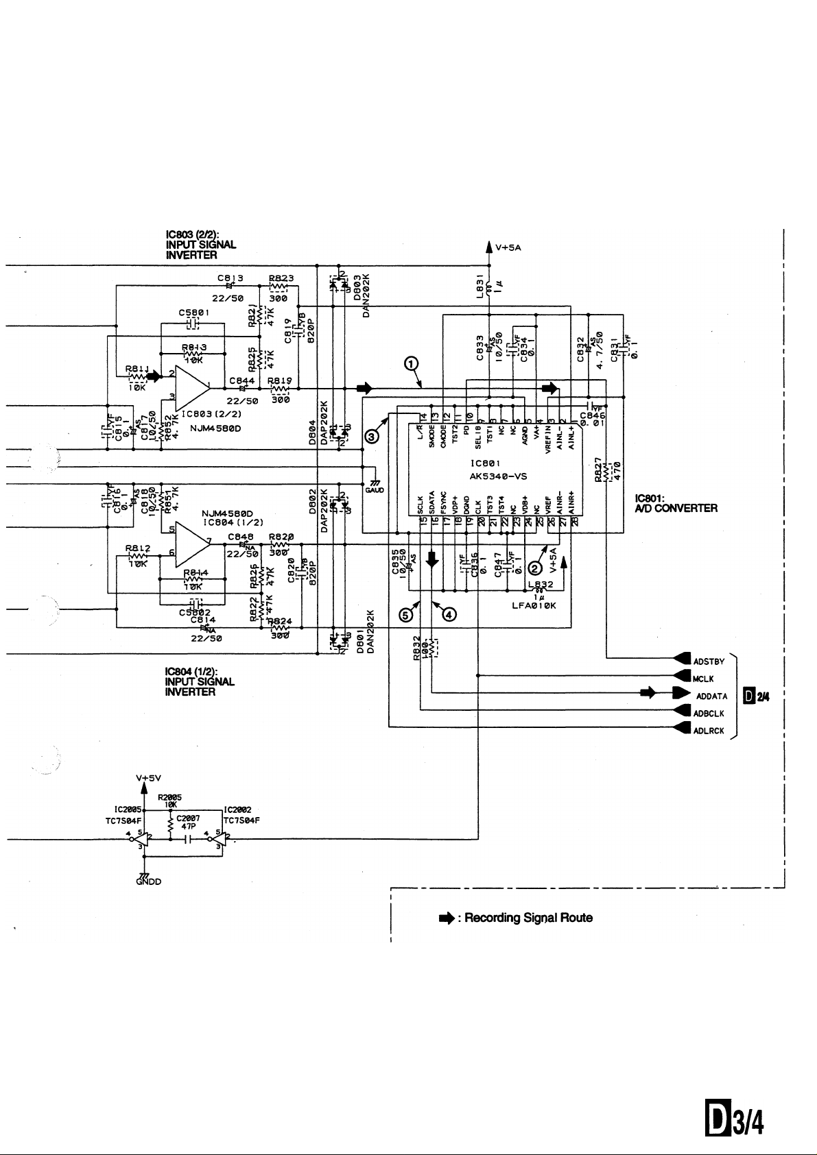
(T) 1C801 pin 2
^ (ADCLDATA)
©
pin 27
RDATA)(ADC
During REC
(Analog 1 kHz OdB)
IV/div ImS/div
(?) IC401 pin9(LRCK)
(t) IC401 pin 8 (SDATA)
IC401 pin? (BiCK)
During REC
lOV/cSv 2pS/div
(ÍÍ) ÍC302 pin 9 (VCO iN)
1V/div
1V/div
(12) IC302 pin 4 (VCO OUT)
IC302 F
>< lOV/div
lOV/div
IC301 pii
(13) ÍC301 pin 80 (EC ERR)
10V/div
During REC 50nS/div
©■
OAAAAAAAAA/V
® ^/\J\r\/\r\f\f' ÍIgnd
--------------------
(3) IC801 pin 14 (ADC LRCK)
IC801 pin 16 (ADC DATA)
(D IC801 pin 15 (ADC BCK)
During REC (1kHz OdB)
lOV/div 2riS/div
©
©
©
♦-GND
-GND
GND
ND
(9) IC304 pin 9 (AO)
@ IC304pin1 (I/O)
Optical input during REC
5V/div 0.2iiS/div
©
0
v\5) IC301pin4
^ (DIN2 : COAX IN)
-GND
-GND
0
- -GND
IC301 pin 1
PN1 : OPT IN)
Optical, coaxial and
simultauieous input
During REC
lOV/drv 0.2jiS/div
(IS) s-
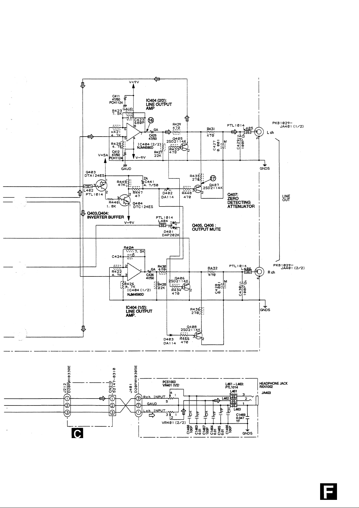
IC404pin7
>< (LIN oDt Lch) 5V/div
(179 0407 (Emitter) 5V/div
nW IC406pin7
^ (HPOUTLch)10V/div
During PLAYBACK
(CD llcHz)
0.5mS/div
© ^\/\/\/\y -^GND
© vAAA/'
© \/\/\/\/^ -»-GND
-GND
-GND
30
Page 31

PDR-04
IC301 (LC89585)[V]
Pin
No.
1 0 0 0
2 0 0 0
3 0 0 0
4 0 0 0
5
6 2.4 2.4
7 5.0 5.0 5.0
8
9 0
10 2.5 2.5 2.5
11 2.5 2.5 2.5
12
13
14 2.0 2.3
15 0 0 0
16 0
17
18 0 5.0
19 0 5.0 5.0 69 0 0 0.8
20 5.0 5.0
21 0 0
22 0 0
23 0 0
24 0 0
25 0 0
26 2.4 2.4
27 2.4 2.4
28 2.4 2.4
29 5.0 5.0 5.0
30 0 1.6
31 2.0 2.0
32 2.5 0
33 0 0
34 0 0.6
35 2.0
36
37 0 5.0
38 2.2 2.2
39
40 0 0 0
41 5.0 5.0 5.0
42
43 2.0 2.2
44 0 2.4 0 94 0.2 0
45 2.0 2.0 2.0 95 0 0
46 2.5 2.5
47 2.4 2.4
48
49 0 0
50 4.9 4.9
MODE
STOP PLAY REC
2.4 2.4
1.8 1.8
0
0 0 0
5.0 5.0
0 0
0 0
2.0 2.0
0 2.5 2.5 86 0 0 0.6
2.7 2.7 2.6 89 5.0 5.0 5.0
2.0 2.0 2.2
2.0 2.0 2.1 98 4.9 4.8
Pin
No.
51 0 0
52
53 5.0 5.0
54 0 0 2.3
2.4
55 0 0 2.3
2.4
56
57
1.8
58
0
59
60 0 0
61
62
5.0
63 0 0 1.4
2.4
64 0 0 1.3
65
66 5.0 5.0 2.0
0
67 5.0 5.0 4.1
5.0
68
5.0
70 0 0 0
0
71 0 0 0.7
0
72
0
73
0
74 0 0 0
0.1
75 5.0 5.0 5.0
5.0
76 2.6 0 2.5
Oto
77 2.7 5.0 2.7
3.4
0 to
78
24
79 2.4 0
0
80 0 5.0
22
81 0 0
2.5
82 0 0 0
0.6
83 5.0 0
0.6
84
85
0
87 0 0 0.7
2.2
88
90
91
92
2.2
93
2.5
96
2.4
97 4.8 4.8
0
99 0.6 2.3
4.9
100 5.0
MODE
STOP PLAY REC
5.0
5.0
0
0
0
0
0
0
0
0
5.0
5.0
0
0
0 0 2.4
0 0 0.9
0 0 0
0 0
2.4 0 2.4
0
0
0 0 3.1
0 0 1.9
0 0 0
1.4 5.0
5.0 5.0
5.0 4.9
0 0
5.0 5.0
IC302 (CD74HC4046AM) [ V ] IC404 (NJM4580D) [ V ] IC801 (AK5340-VS)[\/]
MODE
Pin
No.
0
3.9
4.1
2.4
2.5
2.5
2.5
2.4
5.0
0
STOP
1 5.0
2
3 0
4 2.5
5 0
0.7
6
7
0.7
8
2.5
9
10
11 2.5
12 AA
13 0
14 0
5.0
15
16 5.0
0
0
0
IC304 (MB81C4256A-70PJ)[V]
Pin
No.
1 0 0 1.4
0
2.4
0
0
5.0
4.9
1.3
5.0
4.9
0.3
0
0
4.8
4.8
2.3
2
3 5.0 5.0 4.1
4 5.0 5.0 2.0
5 0 0 2.5
6
7 -
8
9 0 0
10 0 0 1.4
11 0 0
12
13
14 0 0
15 0 0 2.5
16
17 0 0 2.5
18 0 0 2.5
19
20
21
22
23
24 0 0 0.9
25
26 0 0 0
IC803(NJM4580D)[V3
Pin
No.
1
2
3
4 -9 -9 -9
5 0 0 0
6
7
8
MODE
STOP PLAY
0 0 1.4
- -
_
0 0
5.0 5.0
0 0 2.5
- - -
- - -
- - -
5.0 5.0 4,1
5.0 5.0 3.9
0 0 0.8
MODE
PLAY
STOP
0 0 0
0 0 0
0 0 0
0
0 0
0 0
9 9 9
REC
-
-
-
1.3
2.5
2.5
5.0
2.5
REC
0
IC804(NJM4580D)[V]
STOP
0
-9 •9
0 0
0 0
MODE
PLAY
0 0
REC
-9
0
0
Pin
No.
1 0 0 0
2
3 0 0 0
4
5 0 0 0
6
7
8 9 9 9
Pin
No.
1 0 0
2
3 1.2 1.2
4 -9
5 0 0
6
7
8 9
IC406 (MS218AFP) [V]
Pin
No.
1 0 0
2
3
4
5 0
6 0 0 0
7 0
8 9
Q301 (DTA114TS)[V] Q403 (DTA124ES) [ V]
Pin
No.
E 5.0
C OS 0.4
B
Q303(DTA114TS)[V ] Q404 (DTC124ES) [ V ]
Pin
No.
E 5.0
C
B
Q304 (DTC114ES)[V3 Q405 (2SD2114K) [ V ]
Pin
No.
E 0
C 2.0
B 02
Q401 (DTC124ES)[V]
Pin
No.
E
C 14
B -9
Q402 (DTA114ES)[V]
Pin
No.
E
C -9
B
MODE
PLAY
STOP
1.2
1.2
-9
0 0
0 0
9
MODE
PLAY
STOP
0 0
0 0
-9 -9
0
0
9
MODE
PLAY
STOP
5.0
5.0 5.0 5.0
MODE
PLAY
STOP
5.0
0.9 0.8 0.8
5.0 5.0 5.0
MODE
PUY
STOP
0
-
-0.1 to
0
MODE
PLAY
STOP
-9 -9 -9
-9
2.0 2.0
MODE
PLAY
STOP
5.0
5.0
5.0
5.0 3.6 3.6
REC
1.2
1.2
REC
REC
5.0
0.4
REC
5.0
REC
REC
REC
5.0
Pin
0
-9
0
0
0
9
0
0
0
-9
0
0
9
0
-
0
No,
1 2.5 2.5
2 2.5 2.5 2.5
3 5.0 5.0 2.4
4 5.0 5.0 0
5 0 0
6 0 0
7 0 0 0
8 0 0 0
9 0 0 0
10 5.0 5.0 0
11 0
12 5.0 5.0 5.0
13 0 0 0
14
15 2.0 2.0
16 0
17 5.0
18 5.0
19 0
20 2.1 2.1 2.1
21 0
22
23 0
24 5.0
25 0 0 0
26
27 2.5 2.5 2.5
28 2.5 2.5 2.5
Pin
No.
E
C -9 5,0 5.0
B 5.0
Pin
No.
E
C -9
B
Pin
No.
E
C
B
MODE
PLAY
STOP
2^
0 0
5.0 5.0 2.4
STOP PLAY REC
5.0 5.0 5.0
STOP
5.0 5.0 5.0
5.0
STOP
-9 -9 -9
1.1 -9 -9
-9
0
2.5
0
5.0
5.0
0
0
0
5.0
MODE
0.2
MODE
PLAY
5.0
0.2
MODE
PLAY
3.7
REC
2.5
2.5
2.2
2.5
5.0
5.0
5.0
REC
REC
0
0
0
0
0
0
0
0.2
5.0
0.2
3.7
Q406 (2SD21 UK) [ V ]
STOP
-9
-9
MODE
PLAY REC
-9
-9 -9
3.7
-9
3.7
Pin
No.
E
-9
C 1.1
B
Q408 (2SD2114K) [ V ]
Pin
No.
E 0
5.0
C
B
MODE
STOP PLAY
0 0
0 0 0
0.6
-0.7
REC
-0.1
31
Page 32

PDR-04
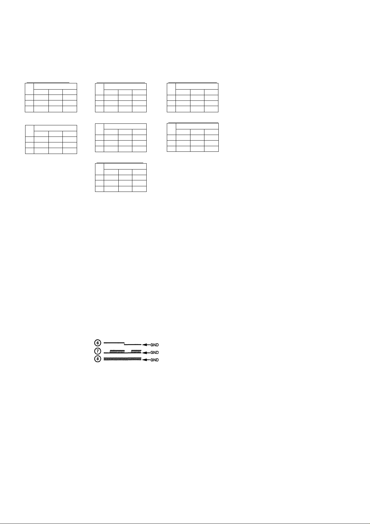
4. PCB CONNECTION DIAGRAM
NOTE FOR PCB DIAGRAMS :
1. Part numbers in PCB diagrams match those in the schematic
diagrams.
2. A comparison between the main parts of PCB and schematic
3. The parts mounted on this PCB include all necessary parts for
several destinations.
For further information for respective destinations, be sure to
check with the schematic diagram.
4. View point of PCB diagrams.
Connector Capacitor
(zi#.-:7ir) (a>-r>+h)
4.1 MECHANISM AND HEAD BOARD ASSEMBLIES
VR104
VR115
VR105
VR108
VR107
VRl
VR10
VR119
VRH1
VR106
VRl 12
VRl 10
VR103
IC202
IC203
Q111
0109
1C102
IC103
0113
32
Page 33

HEAD BOARD ASSY
PDR-04
0102
0115
0117
0116
0107
IC101
0106
0104
0101
0109
0105
0103
0108
IC104
0110
3« V "O- JS
0 -^-O i/'-i
«a« ITS.- 3 O'
il. 0
C C
-O
(PNP1418-A)
MECHANISM
BOARD ASSY
SIDEB
AlB
33
Page 34

PDR-04
4.2 SERVO UCOM BOARD ASSY
H SERVO UCOM BOARD ASSY
O 0 O o]
o
'CNl
i to o ol
........
i.rrB«v
p 0 o ol 1
..............
^
è èÈ
JS05
................
^'sK3Ì0
...............................
0
' ...........................................
:
£CC:' ■ c ;
] = C . --1
C3
■■■■ a,, ■
n
kSig
3.IWT1
4, -N'?
S:.
'
'03
O
Q5026
IC207
IC206
RS66
C289
Rg67
IC355
13
IC354
CN301
IC208
IC358
IC357
1C205
IC360
Q208
Q280
IC5024
IC311
IC361
Q201
IC201
34
13
CN701
(PNP1418-A)
SIDE A
Page 35

IC359
IC352
IC204
IC362
1C363
1C353
PDR-04
SERVO UCOM BOARD ASSY
IC356
Q14
Q13
IC5008
Q202
Q203
IC351
(PNP1418-A)
SIDEB
35
Page 36

PDR-04
4.3 AUDIO DIGITAL AND STRATEGY SMALL BOARD ASSEMBLIES
H AUDIO DIGITAL BOARD ASSY
IC408
Q403
Q404
Q405
Q407
IC407
IC404
IC401
Q408 Q406
Q401 Q3002
0402 03001
IC406
IC338
IC33I
IC333 03006
IC340 03005
IC342
IC334
IC302
IC304
IC34I
IC339
1C 301
03007
IC335
IC312
IC337
IC308
IC305
0304 0301
IC309
0303 IC3001
IC303
IC2002 1C2005
IC803
1C 801
IC804
Page 37

AUDIO DIGITAL BOARD ASSY
PDR-04
SIDE B
37
Page 38

PDR-04
4.4 FUNCTION, POWER A AND POWER B BOARD ASSEMBLIES
POWER A BOARD ASSY
□
CN303
AC POWER CORD
38
GlH
(PNP1393-D)
SIDE A
Page 39

PDR-04
Page 40

PDR-04
4.5 ALC AND HEADPHONE BOARD ASSEMBLIES
ALC BOARD ASSY
SIDE A
HEADPHONE BOARD ASSY
-------------------------------
o
K№U/
ft-
.fib
PWZ3590-
^wz34se-
O
CN211
1 I
SK5V0
--------------------------------
■B-
so ci|ti
-VR40i
CI39J ■"
o
cn-
Utm
ALC BOARD ASSY
HEADPHONE BOARD ASSY
SIDEB
40
E F
Page 41

5. PCB PARTS LIST
NOTES: • Parts marked by *NSP" are generally unavailable because they are not in our Master Spare Parts List.
• The ^ mark found on some component parts indicates the importance of the safety factor of the part.
Therefore, when replacing, be sure to use parts of identical designation.
• When ordering resistors, first convert resistance values into codeform as shown in the following examples.
Ex.l When there are 2 effective digits (any digit apart from 0), such as 560 ohm and 47k ohm (tolerance is shown by J-5%,
andK=:10%).
560 n 56x10' 561
47kD. -► 47x10' -► 473................................................................................................................................................................RD1/4PU\À]\7]{^J
0.5 a -► R50........................................................................................./?a^2h1II[I1!IIa:
la -► iRO..............................................................................
Ex.2 When there are 3 effective digits (such as in high precision metal film resistors).
5.62kQ -► 562x10' 5621
................
............................................
.........................................................
RD1/4PU [Hll]|I] 7
RN1/4PCMEM\1\F
PDR-04
Mark No.
Description Part No.
LIST OF ASSEMBLIES
NSP MOTHER BOARD ASSY PYY1209
NSP h HEAD BOARD ASSY PWZ3386
NSP - ALC BOARD ASSY PWZ3389
NSP - HEADPHONE BOARD ASSY PWZ3390
NSP L mechanism BOARD ASSY PWZ3391
NSP auD 10 DIGITAL BOARD ASSY PWZ3388
NSP •- SERVO UCOM BOARD ASSY PWZ3387
NSP STRATEGY SMALL BOARD ASSY PWX1518
NSP SUB BOARD ASSY PWX1505
HEAD BOARD ASSY PYY1211
-AUDIO DIGITAL BOARD ASSY PYY1212
LSERVO UCOM BOARD ASSY PYY1214
-FUNCTION BOARD ASSY PWZ3042
- POWER A BOARD ASSY PWZ3354
L POWER B BOARD ASSY PWZ3359
MOTHER BOARD ASSY
OTHERS
PC BOARD PNP1418
MECHANISM BOARD ASSY
SEMICONDUCTORS
D1001
PCI 001
GP1S24
NX5803K-F1
RESISTORS
All Resistors
Rsi/iosnnnj
OTHERS
J1002 CONNECTOR ASSY 7P
PDE1260
! HEAD BOARD ASSY
SEMICONDUCTORS
A
A
I Cl 02,I Cl 04
IC202
IC203
ICIOI
I Cl 03
BA4560F
LA6517
LA6520
PA4022A
TC7S08F
Mark No.
0103-0106 2SA1037K
0107,0108 2SA1461
0102 2SB1189
0101 2SC2412K
QUO 2SJ146
0115 DTA114EK
0111 DTA114TK
0117 DTA124EK
0116 DTC114TK
0109 DTC114TS
0113 DTC144TS
D101 DAI 14
DUO UDZ6.2B
Description
CAPACITORS
Cl03, Cl42, Cl 45, Cl46 CCSQCH100D50
Cl23,Cl 24 CCSQCH221J50
C109-C112 CCSQCH391J50
Cl47, Cl 48 CCSQCH471J50
Cl 22 CCSQCH620J50
Cl 40 CCSQCK2R0C50
C105-C108 CCSQSL821J50
Cl 16 CEJA100M16
Cl 01, Cl 02, Cl 13, Cl 21, Cl 25 CEJAl 01 Ml 0
C221,C224, C227, C230 CEJA470M16
Cl 17 CEJANP1R0M50
Cl 27 CEJANP4R7M16
Cl 33 CRXA103J50
Cl 14, Cl 30, Cl 31, Cl 37, Cl 38 CKSQYBl 03K50
C141 CKSQYB103K50
Cl 28 CKSQYBl82K50
Cn CKSQYB683K25
Cl04, Cl 18, Cl 20, Cl26 CKSQYF103Z50
Cl 34, Cl 35, Cl 39, Cl 64, Cl 89 CKSQYF103Z50
C220,C222, C223, C225,C226 CKSQYF103Z50
C228,C229,C232 CKSQYF103Z50
Cl15,Cl 32,Cl 87 CKSQYFl04Z25
C9 CKSRYB392K50
Cl 44 CKSRYF103Z50
RESISTORS
R130 (62n) PCN1037
R148 (2.2kD) PCN1038
R1104 (2.2ka) PCN1039
R138,R162 RN1/10SE1202D
R136,R161 RN1/10SE3002D
Part No.
41
Page 42

PDR-04
Mark No. Description
R2 RS1/16S104J
R135 RS1/16S132J
R6 RSI/168133J
R1106 RS1/16S202J
Rn05 RS1/16S222J
R134 RS1/16S362J
R12 RS1/16S471J
R8 RS1/16S472J
VRIO (2.2ka) RCP1019
VR1, VR103-VR105, VRl 07 (1 Oka) RCPl 045
VR108,VR112,VR115 (lOkn) RCPl 045
VRl06, VRl11 (22kn) RCPl046
VRl 10, VRl 19 (47ka) RCPl 047
Other Resistors RSl/lOSOODJ
OTHERS
CN106 2H CONNECTOR lOP SIOB-ZR
CN105 ZH CONNECTOR 13P S13B-ZR
CN107 KR CONNECTOR S6B-PH-K-S
PCB BINDER VEF1008
I SERVO UCOM BOARD ASSY
SEMICONDUCTORS
IC5008
IC201
IC206
IC204,IC5024
IC353
IC352
A IC208
IC205
IC351
IC356
IC207
IC311
IC361
IC357,IC358
IC354
IC355, 1C359, 1C362
IC363
IC360
Q203
Q202
Q14
Q201
013,0280
0208
05026
D353
D354
D206
D1351
D210
D202,D205
CAPACITORS
C291
C1308,C284,C295
C247-C257
C355,C356
C282
Part No.
BA4560F
CXA13720
CXD2500B0
HD74HC4053FP
HD74HC573FP
LH5116NA-10
LM2940CT-5.0
PA9004A
PD4785A
PD4786A
PDJ006A
PST529C
PST572E
TC74HC367AF
TC7S00F
TC7S04F
TC7S14F
PYY1196
2SA1037K
2SC2412K
DTA124EK
DTA124ES
DTC114TK
DTC114TS
DTC124ES
1SS133X
DAI 14
DA204K
DAN202K
DAP202K
MTZJ3.9BX
CCS0CH100D50
CCS0CH101J50
CCS0CH121J50
CCSOCH150J50
CCSRCH101J50
Mark No.
Cl 2 CCSRCH270J50
C241 CEAS100M50
C209,C212,C290 CEAS101M6R3
C278 CEAS1R0M50
Cl 302,C264,C271 CEAS2R2M50
C205,C235-C238, C293,C5016 CEAS470M10
C5018 CEAS470M10
C240 CEAS471M10
C351,C358 CEAS471M6R3
C203,C207 CEAS4R7M50
C288 CEASR47M50
Cl 8 CKS0YB102K50
Cl 310, C201, C202, C204, C206 CKSOYBl04K25
C274 CKSOYBl04K25
C5004 CKS0YB222K50
Cl 309 CKS0YB272K50
C5013 CKS0YB333K50
Cl 304 CKS0YB471K50
C260 CKS0YB683K25
C233,C234,C239, C242, C280 CKSOYFl03Z50
C5017,C5019 CKSOYFl03Z50
Cl 301,Cl 307,C285, C292, C352 CKSOYFl04Z25
C357 CKSOYFl04Z25
C283 CKS0YF473Z50
C279 CKSRYB102K50
C208,C210,C213, C218,C289 CKSRYBl03K50
C287 CKSRYBl52K50
C258 CKSRYB223K25
C267-C270 CKSRYB331K50
C219,C262 CKSRYB332K50
C211,C217 CKSRYB333K16
C5005-C5008 CKSRYB471K50
C214,C215 CKSRYB472K50
C216,C261,C286 CKSRYB473K16
C259 CKSRYB681K50
Cl202, C353,C354, C360, C370 CKSRYFl03Z50
Cl 305, Cl 306, C359 CKSRYFl04Z25
C281 CKSRYF473Z25
C272,C273 C0MA104J50
C361 (0.22F,5.5V) PCH1131
C263, C275-C277 (0.33^iF, 16V) PCLl 043
C5002,C5011 (0.15^F,16V) PCLl044
C1201 (0.082iiF,16V) PCL1045
C243 (0.1jliF,16V) PCLl 046
RESISTORS
R1, R1212, R1214, R297,R32 RSI/16S0R0J
R1381-R1388,R280 RSI/16S1OIJ
R233,R5007 RS1/16S102J
R1215,R1308,R213,R214,R216 RSI/16S103J
R247, R248,R256-R259,R266 RS1/16S103J
R268,R5006 RS1/16S103J
R251, R260,R267 RSI/16S104J
R206,R241 RS1/16S105J
R253,R254 RS1/16S114J
R353-R361 RS1/16S124J
R208,R232 RS1/16S133J
R281 RS1/16S181J
R201 RS1/16S184J
R210 RS1/16S204J
R5022 RS1/16S221J
Description Part No.
42
Page 43

PDR-04
Mark No. Description
R5023
R1202,R1204,R234,R236
R203,R212
R211,R242
R270
R252
R243
R1206
R215,R217
R1205,R218
R1351 -R1354, R1356-R1358, R1360
R246,R373,R377,R379-R383
R389-R391, R393-R399
R235,R237
R209
R238
R255
R249
R269
R202,R204
R250
R205
R207
R5025
VR201,VR202 (lOkil)
Other Resistors
OTHERS
CN202
WT 5P CONNECTOR
CN211
CN5021
X352 CERAMIC RESONATOR(16MHz)
X351 CERAMIC RES0NAT0R(4.19MHz) VSS1014
3P JUMPER CONNECTOR
3P TOP POST
KR CONNECTOR 5P
CN203
CN204 6P TOP POST
CN206 5P SIDE POST
J222 LEAD WIRE UNIT
CN205 FFC CONNECTOR 39P
J201 CONNECTOR ASSY 13P
J210 CONNECTOR ASSY 10P
J214 CONNECTOR ASSY 2P
J213 CONNECTOR ASSY 4P
JA203 MINI JACK
PCB BINDER
I AUDIO DIGITAL BOARD ASSY
SEMICONDUCTORS
IC401
IC801 AK5340-VS
IC302
IC301 LC89585
IC406 M5218AFP C3011,C304,C311,C313, C316 CKS0YF104Z25
IC304
IC404, IC803, IC804 NJM4580D C831,C834,C836, C847
A
IC407 NJM7809FA C401,C404,C469
IC408 NJM79M09FA
A
IC303
IC309, IC336 TC74HCOOAF
IC338 TC74HC04AF
IC331 TC74HC08AF C317,C329 (1цF/16V) Pai047
IC335 TC74HC123AF
IC337
Part No.
RS1/16S222J
RS1/16S273J
RS1/16S274J
RS1/16S302J
RS1/16S332J
RS1/16S333J
RS1/16S362J
RS1/16S393J
RS1/16S470J
RS1/16S472J
RS1/16S473J
RS1/16S473J
RS1/16S473J
RS1/16S512J
RS1/16S514J
RS1/16S562J
RS1/16S563J
RS1/16S624J
RS1/16S682J
RS1/16S683J
RS1/16S684J
RS1/16S754J
RS1/16S823J
RS1/16S912J
RCP1045
RS1/10Snnnj
173981-5
52147-0310
B3P-SHF-1AA
B5B-PH-K-S
B6P-SHF-1AA
BS5P-SHF-1AA
DB015NT0
HLEM39S-1
PDE1264
PDE1269
P(k)2KA-E15
PG04KA-E25
PKN1005
PSS1010
VEF1008
AK4321-VF C403
CD74HC4046AM
MB81C4256A-70PJ
PCX1021 C318
TC74HC164AF C343,C405,C408 (47nF/10V) RCH1139
Mark No.
IC308,IC313 TC74HCU04AF
IC2002,IC2005 TC7S04F
IC341,IC342 TC7S32F
IC333, IC334,IC340 TK16124M
0405-0408 2SD2114K
0402 DTA114ES
0301,0303 DTA114TS
0403 DTA124ES
0304 DTC114ES
0401,0404 DTC124ES
D302 1SR35-100AVL
D402,D403 DA114
D801,D803 DAN202K
D401,D802,D804 DAP202K
COILS
L831,L832 LFA1R0K
L301-L306,L308,L311,L312 PTL1014
L316, L328, L329,L402 PTL1014
L404-L408 PTL1014
L330 EMI FILTER PTL1020
CAPACITORS
C383,C429, C430,C445,C446 CCS0CH101J50
C477,C480,C801,C821 CCS0CH101J50
C803,C804 CCS0CH121J50
C308,C331 CCSRCH120J50
C330 CCSRCH180J50
C309 CCSRCH270J50
C2007, C319, C365 CCSRCH470J50
C3007 CCSRCH820J50
C339,C341 CEAS100M50
C817,C818,C833,C835 CEAS100M50
C385 CEAS101M25
C302,C306,C310,C314,C324 CEAS101M6R3
C332,C335,C402 CEAS101M6R3
C805,C806 CEAS220M50
C811-C814, C842-C844,C848 CEAS220M50
C411,C412 CEAS221M25
C315, C323, C328 CEAS470M10
C471,C472 CEAS470M16
C407,C409 CEAS471M6R3
C441,C832 CEAS4R7M50
C347 CKCYB101K50
C348,C823 CKCYF473Z50
C301 CKSOYB102K50
C421,C422,C425,C426 CEZA470M50
C305 CKSQYB103K50
C312,C390 CKSQYB472K50
C303,C307,C333,C334 CKS0YB473K25
C819,C820
C807-C810,C846
C322,C325, C327,C342,C344
C376,C406,C410, C815,C816
C3006, C3009, C3010, C3012, C3013
C3015,C3017,C3019-C3021
C427,C428
C481,C482 (3300|iF/16V)
Description Part No.
CKS0YB473K50
CKS0YB821K50
CKSQYF103Z50
CKSOYF104Z25
CKSQYF104Z25
CKS0YF104Z25
CKS0YF104Z50
CKSRYB103K50
CKSRYF104Z25
CKSRYF104Z25
C0MA102Z50
DCH1057
43
Page 44

PDR-04
Mark No. Description
RESISTORS
R421,R422
R423,R424
R342
R1336, R3015,R3020,R3101
R318,R319,R323,R324,R328
R341,R486
R300,R3n,R329,R331
R1450,R2005,R339
R320
R305
R1333
R3009
R1335,R499
R301
R302
R347,R348
R345
R1324,R303
R1323
R312,R330
R1401-R1404
VR301 (ioidi)
Other Resistors
OTHERS
CN401 3P JUMPER CONNECTOR 52147-0310
CN317 CONNECTOR 8P
CN801 CONNECTOR 9P
CN331 2P TOP POST
CN315 KE CONNECTOR 4P B4B-PH-K-S
JA301 OPTICAL TRANS. MODULE
JA303 OPTICAL TRANS. MODULE
JA401,JA801 2P JACK
KN302 SCREW TERMINAL PNB1558
X301 CRYSTAL RESONATOR
(16.9344MHz)
PCB BINDER
f3 ALC BOARD ASSY
SEMICONDUCTORS
IC2001
A IC2003
A IC2004 NJM79L05A
CAPACITORS
C2001,C2003,C2005
C2002,C2004,C2006, C2008
RESISTORS
All Resistors RSl/lOSDDDJ
OTHERS
CN2001 CONNECTOR 8P 9115S-08L
CN2002 CONNECTOR 9P
Part No.
RN1/10SE1002D
RN1/10SE1602D
RS1/16S0R0J
RSI/168101J
RS1/16S101J
RS1/16S101J
RSI/168102J
RS1/16S103J
RS1/16S105J
RS1/16S151J
RS1/16S221J
RS1/16S222J
RS1/16S271J
RS1/16S333J
RS1/16S363J
RS1/16S472J
RS1/16S473J
RS1/16S512J
RS1/16S622J
RS1/16S681J
RS1/2LMF270J
RCP1045
RSl/lOSDDDJ
9115B-08
9115B-09
B2P-SHF-1AA
GP1F32R
GP1F32T
PKB1029
PSS1008
VEF1008
LM1972M
NJM78L05A
CEAS100M50
CKSQYF104Z25
9115S-09L
Mark No.
Description
[HEADPHONE BOARD ASSY
COILS
L461-L463
CAPACITORS
C1466-C1468
C1463-C1465
Cl 469
RESISTORS
VR401 VARIABLE RESISTOR (5kii)
OTHERS
JA403 HEADPHONE JACK
SUB BOARD ASSY
OTHERS
PC BOARD
FUNCTION BOARD ASSY
SEMICONDUCTORS
0701-0704
D701-D703,D706 SEL6210S
r^r\U C
L701,L702 FERRITE BEADS VTH1020
SWITCHES
S701-S718 PSG1006
CAPACITORS
C704
C702
RESISTORS
All Resistors
OTHERS
IC701 REMOTE RECEIVER UNIT GP1U27X
CN701 FFC CONNECTOR 39P HLEM39R-1
V701 FL INDICATOR TUBE
fil POWER A BOARD ASSY
SEMICONDUCTORS
A IC904
A D901-D908 11ES2
COILS
L902 FERRITE BEADS
A L11 LINE FILTER
CAPACITORS
C901,C902,C914,C915
C904-C906, C911 (3300nF,16V)
A C71,C78 (100pF,400V AC)
RESISTORS
All Resistors
A C72,C75 (0.01nF,400V AC)
Part No.
PTL1014
CCSQCH101J50
CKSQYF103Z50
CKSQYF473Z50
PCS1003
RKN1002
PNP1393
DTA124ES
CKCYB101K50
CKCYF103Z50
RD1/4PUDDDJ
PEL!086
UPC24M05AHF
VTH1020
VTL1008
CKCYF103Z50
DCH1057
PCL1040
VCG-044
RD1/4PUDDDJ
44
Page 45

PDR-04
Mark No.
Description
OTHERS
A FUSE aiP
A
cm 2
J901
J12
A
cmi
J905
POWER B BOARD ASSY
SEMICONDUCTORS
IC11-IC15
A
IC23
A
A
IC22
A
D11-D14,D52
D54
A
COILS
L21-L23 FERRITE BEADS
CAPACITORS
C52
C54
C28,C29
C11,C13,C15-C18
C23,C24
C26 (3300^iF,16V)
C25 (10000hF,16V)
RESISTORS
Other
OTHERS
cm 5
CN17
A J1
J16
2P-VH CONNECTOR
EARTH LEAD UNIT
CONNECTOR
TERMINAL
PCB BINDER
Resistors
5P JUMPER CONNECTOR
KR CONNECTOR 5P
CONNECTOR ASSY 2P
CONNECTOR 6P
PCB BINDER
EARTH METAL
Part No.
AKR1003
B2P3-VH
PDF!175
PF07PG-D10
RKC-061
VEF1040
PDF1176
ICP-NIO
LM2940CT-5.0
NJM7905FA
11ES2
MTZJ20A
VTH1020
CEAS101M35
CEAS470M35
CEAS471M10
CKCYF103Z50
CQMZA472J50
DCH1057
VCH1124
RDl/4PUnnnj
52147-0510
B5B-PH-K-S
PDE1273
PF06PG-D15
VEF1008
VNF-091
Mark No.
Description
STRATEGY SMALL BOARD ASSY
SEMICONDUCTORS
IC343
IC344
03508
03501-03507
D332
D331
CAPACITORS
C3520
C344,C3519,C3521
RESISTORS
R3514
R3504
R3510
R3511
R3505
R3503
R3502
R3520
R3506
R3513
R3507
R3512
R3501
R3508
VR3502,VR3503 (lOkii)
VR3501 (47ka)
Other Resistors
OTHERS
CN3502
CN3506
PH C0NNEa0R(2P)
PH CONNEaOR(6P)
Part No.
TC74HC138AF
TC7S04F
2SC2412K
DTA124TK
1SS355
UDZ3.0B
CEV470M16
CKSQYF103Z50
PCN1039
RN1/10SE1502D
RN1/10SE1601D
RNV10SE1800D
RN1/10SE1801D
RN1/10SE1802D
RN1/10SE2201D
RN1/10SE2400D
RN1/10SE2401D
RN1/10SE2701D
RN1/10SE4701D
RN1/10SE5100D
RN1/10SE5101D
RN1/10SE6201D
PCP1042
PCP1043
RSViosnnnj
B2B-PH-SM3
B6B-PH-SM3
45
Page 46

PDR-04
6. ADJUSTMENT
6.1 ADJUSTMENT METHODS
If a compact disc recorder is adjusted incorrectly or inadequately, it may malfunction or not work at all even though there
is nothing at all wrong with the pickup or the circuitry. Adjust correctly following the adjustment procedure.
# Measuring instruments and Tools
(1 ) Dual trace oscilloscope (10:1 probe) (6) Resistor (1 OOkQ)
(2) Low-frequency oscillator (7) Hexagonal screwdriver (1.27mm diagonal)
(3) Test disc (STD-903), (STD-R03) (8) Standard tools
(4) Low-pass filter (15kQ + 0.001 jxF), (39kQ + 0.001 pF) (9) Small screwdriver
(5) Hi-pass filter (3.9kD + 180pF) (10) Multimeter (Voltage accuracy : Below 1 mV)
# Adjustment Kerns / Verification items and Order
Adjustment 1
Step
1 Playback Power Adjustment
2 Coarse Focus Offset Adjustment
3 Coarse Skew Adjustment
4 Coarse Grating Adjustment
5
DPP (Tracking Offset) Adjustment
6 Fine Focus Offset Adjustment CN204 (TP201), Pin 1 (RF) VR105 (FE. OFS)
7 Fine Skew Adjustment
8 Grating Re-adjustment
Adjustment 2
Step Item Test Point Adjustment Location
CD-R VCO Control Voltage Adjustment
1
2 Multi Pulse Time Adjustment
3
EFM Rising Edge Time Adjustment
4 3T Falling Edge Time Adjustment
5 WBL+ Offset Adjustment
6 Coarse WBL Offset Adjustment
7 Playback Power Re-adjustment
8 Coarse Focus Offset Adjustment
9 Main and Sub Mix Ratio Adjustment
10 Tracking Amp. Gain Adjustment
11 Tracking Offset Adjustment
12 ACT Offset Adjustment
13 ACT GAIN Adjustment
14 Fine Focus Offset Adjustment
15 WBL BALANCE Adjustment
Item
CN104 (TP1), Pin 7 (PWAJT) VR103 (PB. PW)
CN204 (TP201), Pin 1 (RF)
CN204 (TP201), Pin 1 (RF)
CN104(TP1), Pin3(TE) Grating adjustment slit
CN104 (TP1), Pin 3 (TE) VR112 (TE. OFS)
CN204 (TP201), Pin 1 (RF)
CN104 (TP1), Pin 3 (TE)
CN331 (TP30), Pin 1 (VCOIN)
CN3506, Pin 6 (MPLS) VR3501 (MPLS DLY)
CN3506, Pin 5 (EFM IN)
CN3506, Pin 4 (SEFM)
CN3506, Pin 3 (3T IN)
CN3506, Pin 2 (3T OUT)
CN104(TP1), Pin6(RWBL) VR107 (WBL+. OFS)
CN104 (TP1), Pin 5 (WBL)
CN104 (TP1), Pin 7 (PWAJT) VR103 (PB. PW)
CN204 (TP201), Pin 1 (RF) VR105 (FE. OFS)
CN104 (TP1), Pin 1 (STE)
CN104 (TP1), Pin 2 (MSTE)
CN104 (TP1), Pin 3 (TE) VR111 (TE. GAIN)
CN104 (TP1), Pin 3 (TE) VR112(TE. OFS)
CN5021 (TPOO), Pin 1 (ACT ERR) VR1 (ACT. OFS)
CN5021 (TPOO), Pin 1 (ACT ERR) VR10 (ACT. GAIN)
CN204 (TP201), Pin 1 (RF) VR105 (FE. OFS)
CN104 (TP1), Pin 5 (WBL)
Test Point Adjustment Location
VR105 (FE. OFS)
Radial tilt adjustment screw and
Tangential tilt adjustment screw
Radial tilt adjustment screw and
Tangential tilt adjustment screw
Grating adjustment slit
VR301 (VCO CON)
VR3502 (EFM DLY)
VR3503 (3T DLY)
VR108 (WBL. OFS)
VR110(MS. MIX)
VR106 (WBL. BALANCE)
46
Page 47

PDR-04
Step
16 Fine WBL Offset Adjustment
17 WBL Focus Offset Adjustment
18
Recording Power Adjustment
19
HF Amp. Gain Adjustment
20 Focus Servo Loop Gain Adjustment
Tracking Sen^o Loop Gain Adjustment
21
Item
SERVO UCOM BOARD ASSY
- CN5021 (TPOO)
1: ACT ERR
2: ACT IN
3: V+5A
11, CN5021
(TPOO)
VR202
TE.GAIN
VR201
FCS.GAIN Vg)
Test Point
CN104 (TP1), Pin 5 (WBL) VR108 (WBL OFS)
CN104 (TP1), Pin 5 (WBL)
CN104 (TP1), Pin 7 (PWAJT) VR104 (REC. PW)
CN104(TP1), Pin8(HF)
CN204 (TP201), Pin 5 (FCSIN)
CN204 (TP201), Pin 6 (FCSER)
CN204 (TP201), Pin 2 (TRKER)
CN204 (TP201), Pin 3 (TRKIN)
VR115(WFE. OFS)
VR119(HF. GAIN)
VR201 (FCS. GAIN)
VR202 (TE. GAIN)
Adjustment Location
HEAD BOARD ASSY
VR103
VR10|
ACT.GAlN|
VR1
ACT.OFS
PB-PW
/^VR110
SSiMS.Mix
CNIO4O I
(TP1)
^VR112 LJ
SaTE.OFS
VR105
FE.OFS
VR104
^REC.PW
CN204 (TP201)
1:RF
2: TRKER
3: TRKIN
4: AGNO
5: FCSIN
6; FCSER
VR111
TE.GAIN
VR108
WBL.OFS
VR115»^I^
WFE.OFS VR107
|@)||(^HFGAINn\
WBL+OFS
VR119 \
nx
CN3506
VR106
WBL BALANCE
— CN3506
1 :GND
2 ; 3T OUT
3: 3T IN
4 :SEFM
5 : EFM IN
6 : MPLS
1
CN104 (TP1)
1:STE
2: MSTE
3: TE
4: AGNO
5: WBL
6: RWBL
7: PWAJT
8: HF
nn
GNDm CN331
VCOIN loj (TP30)
VR301
^
a
VCO CON
____«_____
AUDIO DIGITAL BOARD ASSY
nn
Fig. 1 Adjustment points
VR3502
EFM DLYtSSi
o
IVR3501
Isa MPLS DLY
VR3503
3TDLY
CN3502
STRATEGY SMALL BOARD ASSY
47
Page 48

PDR-04
i Notes
(1 ) Use a 10 : 1 probe for the oscilloscope.
(2) All the knob positions (settings) for the oscilloscope In the adjustment procedures are for when a 10 :1 probe is used.
• Test Mode
This model has a test mode so that the adjustments and checks required for service can be carried out easily.
When this model is in test mode, the keys on the front panel work differently from normal. Adjustments and checks can be
carried out by operating these keys with the correct procedure. For this model, all adjustments are carried out in test
mode.
[ Setting to Test Mode ]
Howto set this model into test mode.
(1 ) Unplug the power cord from the AC socket.
(2) Short the test mode short land. (See Fig. 1.)
(3) Plug the power cord back into the AC socket.
When the test mode is set correctly, the display is different from what it usually is when the power is turned on. (lights up
all FL display) If the display is still the same as usual, test mode has not been set correctly, so repeat Steps 1 - 3.
[ Release from Test Mode ]
Here is the procedure for releasing the test mode.
(1 ) Press the STOP key and stop all operations.
(2) Unplug the power cord from the AC socket.
[ Operations of the Keys in Test Mode ]
Code
► PLAY Spindle servo ON
Key Name
DIGITAL
SYNCHRO
FINALIZE
Function In Test Mode
Playback laser diode ON Lights up the laser diode by playback power.
The laser diode is lit up and the focus acutuator Is lowered,
then raised slowly and the focus servo is closed at the point
where the objective lens is focused on the disc.
With the player in this state, if you lightly rotate the stopped
Focus servo closes
disc by hand, you can here the sound the focus servo. If you
can hear this sound, the focus servo is operating correctly.
If you press this key with no disc mounted, the laser diode
lights up, the focus acutuator is pulled down, then the
acutuator is raised and lowered three times and returned to
its original position.
Starts the spindle motor in the clockwise direction and when
the disc rotation reaches the prescribed speed (about 500
rpm at the inner periphery), sets the spindle servo in a
closed loop.
Explanation
48
Page 49

PDR-04
Code Key Name Function In Test Mode
II
◄◄
•
►►
•
►►1
■
▲
0
1
o
PAUSE
MANUAL/
TRACK
SEARCH REV
MANUAL/
TRACK
SEARCH FWD
STOP Stop
OPEN/CLOSE
REC
i
REC MUTE
DISPLAY OFF
WRITE
Tracking sen/o
close/open
Carriage reverse
(inwards)
Carriage forward
(outwards)
Disc tray open/close
Maximum recording
power
Laser diode ON
Focus offset switching
Optical axis servo
switching
Explanation
Pressing this key when the focus servo and spindie servo
are operating correctly in closed loops puts the tracking
servo into a closed loop, displays the track number being
played back and the elapsed time on the front panel.
If the elapsed time is not displayed or not counted correctly,
it may be that something is our of adjustment, or that there is
some other problem.
This key is a toggle key and open/close the tracking servo
alternately. This key has no effect if no disc is mounted.
Moves the pickup position toward the inner diameter of the
disc. When this key is pressed with the tracking servo in a
closed loop, the tracking servo automatically goes into an
open loop.
Since the motor does not automatically stop at the
mechanical end point in test mode, be careful with this
operation.
Moves the pickup position toward the outer diameter of the
disc. When this key is pressed with the tracking servo in a
closed loop, the tracking servo automatically goes into an
open loop.
Since the motor does not automatically stop at the
mechanical end point in test mode, be careful with this
operation.
initializes and the disc rotation stops.
The pickup and disc remain where they are when this key is
pressed.
Open/close the disc tray. This key is a toggle key and
open/close tray alternately.
Pressing this key when the disc is turning stops the disc,
then opens the tray.
This key operation does not affect the position of the pickup.
Lights up the laser diode with maximum recording power and
normal EFM by pressing REC and REC MUTE keys in order.
* The laser diode may be damaged if adjustments are made
before pressing these keys.
Switches the focus offset state.
DISPLAY OFF LED Lights UP : C/N in the best condition
Lights OFF : Jitter in the best condition
Switches the ON/OFF of the optical axis servo.
(MANUAL) LED Lights UP ; Optical axis servo ON
Lights OFF ; Optical axis servo OFF
[ How to Play Back a Disc in Test Mode ]
In test mode, since the servos operate independently, playing back a disc requires that you operate the keys in the correct
order to close the servos.
Here is the key operation sequence for playing back a disc in test mode.
FINALIZE I
PLAY
PAUSE II
Wait at least 2-3 seconds between each of these operations.
Lights up the laser diode and closes the focus servo.
Starts the spindle motor and closes the spindle servo.
Closes the tracking servo.
49
Page 50

PDR-04
6.2 Adjustment 1
6.2.1 Playback Power Adjustment
• Objective
• Symptom when out
To optimize the playback power of the laser diode.
Play does not start, track search is impossible, track are skipped.
Adjustment 1
of adjustment
• Measurement instru
ment connections
Connect the multimeter to
CN104 (TP1), Pin7(PWAJT)
► Player state
»Adjustment
location
»Disc
Test mode.
Playback laser diode ON
VR103 (PB. PW)
(HEAD BOARD assy)
None needed
[ Procedure ]
When adjusting with the multimeter.
(1) Lights up the playback laser diode using the DIGITAL SYNCHRO key.
(2) Adjust the voltage value of Pin 7 (PWAJT) of CN104 (TP1) to the voltage value (PB PW voltage ± 5mV) displayed on the
pickup flexible cable using VR103 (PB PW).
Note) This adjustment cannot be performed accurately If disc Is set. Be sure to remove disc first before adjustments.
Reference: When adjusting with the optical power meter.
(1) Move the pickup to the outer edge of the disc with the MANUAL / TRACK SEARCH FWD ►► key.
(2) Lights up the playback laser diode by DIGITAL SYNCHRO key.
(3) Shine the light discharged from the objective lens in the pickup on the light power meter sensor. Adjust VR103 (PB. PW)
so that the playback laser diode output is an average 0.6 mW ± O.OSmW.
(Wavelength 790nm, Average mode)
Recording on the disc is not possible In test mode.
50
P: Playback power
R: Recording power
Page 51

PDR-04
6.2.2 Coarse Focus Offset Adjustment
' Objective
Symptom when out
To coarse adjust the DC offset voltage of the focus servo circuit for perform the tracking and
slider adjustments correctly.
The model does not focus in, sound broken and the RF signal is dirty.
of adjustment
> Measurement instru
ment connections
Connect the oscilloscope to
CN204(TP201), Pin 1 (RF)
(SERVO UCOM BOARD assy)
[ Settings ] 20 mV/div.
2 mS/div.
DC mode
Player state
• Adjustment
location
• Disc
Test mode,focus and spindle servos
closed and tracking servo open.
VRIOS(FE.OFS)
(HEAD BOARD assy)
STD-903
[ Procedure ]
(1) Press the FINALIZE key, then the PLAY ► key in that order to close the focus servo then the spindle servo.
(2) Adjust VR105 (FE. OFS) so that the amplitude of waveform at CN204 (TP201), Pin 1 (RF) is maximum.
>■.% V>SSSiS v>s
Adjustment 1
Out of adjustment
Optimum adjustment
51
Page 52

PDR-04
6.2.3 Coarse Skew Adjustment
• Objective
• Symptom when out
To coarse adjust the angle of pickup to the disc for perform the grating and DPP
(tracking offset) adjustments correctly.
Sound broken, some discs can be played but not others.
Adjustment 1
of adjustment
»Measurement instru
ment connections
Connect the oscilloscope to
CN204(TP201), Pin 1 (RF)
(SERVO UCOM BOARD assy)
[ Settings ] 20 mV/div.
200 nS/div.
AC mode
• Player state
• Adjustment
location
• Disc
Test mode,focus and spindle servos
closed and tracking servo open.
Radial adjustment screw and
tangential adjustment screw
STD-903
[ Procedure ]
(1) Move the pickup to the position where the radial/tangential adjustment screws will be seen with the MANUAL / TRACK
SEARCH FWD ►► or REV ◄◄ keys so that the radial/tangential adjustment screws can be adjusted.
(2) Press the FINALIZE key, then the PLAY ► key in that order to close the focus servo then the spindle servo.
(3) Adjust the RAD (radial direction) and TAN (tangential direction) adjustment screws alternately with hexagonal screwdriver
(1.27 mm diagonal) to maximize the RF output at CN204 (TP201), Pin 1.
Note : Radial direction and tangential direction mean the direction relative to the disc shown in Fig. 2.
Radial direction
Hexagonal
screwdriver
0
Fig. 2
52
Page 53

PDR-04
6.2.4 Coarse Grating Adjustment
• Objective
• Symptom when out
To align the tracking error generation laser beam spots to the optimum angle on the track.
Play does not start, track search is impossible, tracks are skipped.
Adjustment 1
of adjustment
• Measurement instru
ment connections
Connect the oscilloscope to
CN104 (TP1), Pln3(TE)
This connection may be via a low
pass filter. (See Fig. 3)
[ Settings ] 50 mV/div.
5 mS/div.
DC mode
Player state
• Adjustment
location
Disc
Test mode,focus and spindle servos
closed and tracking servo open.
Grating slit on pickup
STD-903
[Procedure]
(1) Move the pickup to the position where the grating adjustment slit will be seen with the MANUAL / TRACK SEARCH FWD
►► or REV ◄◄ keys so that the grating adjustment can be adjusted.
(2) Press the FINALIZE key, then the PLAY ► key in that order to close the focus servo then spindle servo.
(3) Insert a screwdriver into the grating adjustment slit and adjust the grating to find the null point.
For more details, see next page.
(4) If you slowly turn the screwdriver clockwise from the null point, the amplitude of the wave gradually Increases, then if you
continue turning the screwdriver, the amplitude of the wave becomes smaller again. Turn the screwdriver counterclockwise
from the null point and set the grating to the first point where the wave amplitude reaches its maximum.
Reference : Fig. 4 shows the relation between the angle of the tracking beam with the track and the waveform.
(5) Return the pickup to more or less midway across disc with the MANUAL / TRACK SEARCH ◄◄ key, press the
PAUSE II key and check that the track number and elapsed time are displayed on the front panel. If they are not displayed
at this time or the elapsed time changes Irregularly, check the null point and adjust the grating again.
Fig.3
Small
screwdriver
53
Page 54

PDR-04
Adjustment 1
[ How to find the null point ]
When you insert the small screwdriver into the slit for the grating adjustment and change the grating angle, the amplitude of
the tracking error signal at CN104 (TP1), Pin 3 (TE) changes. Within the range for the grating, there are five or six locations
where the amplitude of the wave reaches a minimum. Of these five or six locations, there is only one at which the envelope
of the waveform is smooth. This location is where the three laser beams divided by the grating are all right above the same
track. (See Fig. 4.)
This point is called the null point. When adjusting the grating, this null point is found and used as the reference position.
Turning the grating counterciockwise
Grating adjustment position
/ Null point
. \
Waveform of
CN104 (TP1), Pin 3 (TE)
Tuming the grating clockwise
ms
6.2.5 DPP (Tracking Offset) Adjustment
• Objective
• Symptom when out
To correct for the variation in the sensitivity of the tracking photodiode.
Play does not playback, track search is impossible, tracks are skipped.
of adjustment
• Measurement instru
ment connections
Connect the oscilloscope to
CN104(TP1), Pin3 (TE)
[This connection may be via a low
pass filter. (15k£2 + O.OOlpF) ]
[ Settings ] 50 mV/div.
5 mS/div.
DC mode
mmmmmm
Null point waveform Maximum amplitude Wavefonn other than the
Note: If the difference between the amplitude of the error signal at the
innemnost edge and outermost edge of the disc is more than 10%,
adjust the grating again.
Fig. 4
• Player state
wavefonn null point
Test mode,focus and spindle servos
closed and tracking servo open.
• Adjustment
location
• Disc
VR112(TE. OFS)
(HEAD BOARD assy)
STD-903
Adjustment 1
[ Procedure ]
(1 ) Move the pickup to the midway across the disc (R = 35mm) with the MANUAL / TRACK SEARCH FWD ►► or REV
MM keys.
(2) Press the FINALIZE key, then the PLAY ► key in that order to close the focus servo then spindle servo.
(3) Line up the bright line (ground) at the center of the oscilloscope screen and put the oscilloscope into DC mode.
(4) Adjust VR112 (TE. OFS) so that the positive amplitude and negative amplitude of the tracking error signal at CN104
When there is a DC
component
54
When there is no DC
component
Page 55

PDR-04
6.2.6 Fine Focus Offset Adjustment
> Objective
Symptom when out
To optimize the DC offset voltage of the focus servo circuit.
The player does not focus in, sound broken and the RF signal is dirty.
Adjustment 1
of adjustment
• Measurement instru
ment connections
Connect the oscilloscope to
CN204(TP201), Pin 1 (RF).
(SERVO UCOM BOARD assy)
[ Settings ]
20 mV/div.
500 nS/div.
AC mode
Player state
• Adjustment
location
• Disc
Test mode, play
VR105 (FE.OFS)
(HEAD BOARD assy)
STD-903
[ Procedure ]
(1) Move the pickup to midway across the disc (R = 35mm) with the MANUAL / TRACK SEARCH FWD ►► ►» or REV
keys.
(2) Press the FINALIZE key, the play ► key, then the PAUSE ll key in that order to close the respective servos and put the
player into play mode.
(3) Adjust VR105 (FE. OFS) so that the 3T waveform at CN204 (TP201), Pin 1 (RF) is maximum.
Out of adjustment
r V •> 'ft ^ , ft- .ft- y :
Optimum adjustment
55
Page 56

PDR-04
6.2.7 Fine Skew Adjustment
• Objective
To adjust the angle of the pickup relative to the disc so that the laser beams are shone straight
Adjustment 1
down into the disc for the best read out of the RF signals.
• Symptom when out
Sound broken, some discs can be played but not others.
of adjustment
• Measurement instru
ment connections
Connect the oscilloscope to
CN204 (TP201), Pin 1 (RF)
(SERVO UCOM BOARD assy)
[Settings] 20 mV/div.
200 nS/div.
AC mode
• Player state
• Adjustment
location
• Disc
Test mode, play
Pickup radial adjustment screw and
tangential adjustment screw
STD-903
[ Procedure ]
(1) Move the pickup to the position where the radial/tangential adjustment screws will be seen with the MANUAL / TRACK
SEARCH FWD ►► or REV ◄◄ keys so that the radial/tangential adjustment screws can be adjusted.
(2) Press the FINALIZE key, then the PLAY ► key to the PAUSE II key in that order to close the respective servos and put the
player Into play mode.
(3) First, adjust the radial adjustment screw with the hexagonal screwdriver (1.27 mm) so that the eye pattern (the diamond
shape at the center of the RF signal) can be seen the most clearly.
(4) Next, adjust the tangential adjustment screw with the hexagonal screwdriver so that the eye pattern can be seen the most
clearly. (Fig. 5).
(5) Adjust in the order of the radial adjustment screw and the tangential screw again, so that the eye pattern can be seen the
most clearly. As necessary, adjust the two screws alternately so that the eye pattern can be seen the most clearly.
(6) After the adjustment, remove the float screw, turn over the servo mechanism assembly, then stabilize the radial adjustment
screw and the tangential adjustment screw with an adhesive.
(Front side)
Stabilize each screw
Hexagonal
screwdriver
56
Page 57

PDR-04
Adiustment 1
Out of adjustment
Optimum adjustment
Out of Optimum Out of
adjustment adjustment adjustment
Fig. 5 Eye pattern
6.2.8 Grating Re-adjustment
Adjust in the same manner as "4. Coarse Grating Adjustment ” in Adjustment 1.
Out of adjustment
Adjustment 1
6.3 Adjustment 2
6.3.1 CD-R VCO Control Voltage Adjustment
• Objective
• Symptom when out
of adjustment
• Measurement instru
ment connections
[ Procedure ]
(1) Adjust VR301 (VCO CON) so that the voltage at Pin 1 (VCOIN) of CN331 (TP30) becomes 2.5 ± 0.1 V.
To optimize the CD-R VCO control voltage adjustment of VCO 1C.
Player does not record or playback CD-R discs.
Connect the multimeter to
• Player state
Test mode, stop
CN331 (TP30), Pin 1 (VCOIN)
(AUDIO DIGITAL BOARD assy)
• Adjustment
location
• Disc
VR301 (VCOIN)
(AUDIO DIGITAL BOARD assy)
None needed
Adjustment 2
57
Page 58

PDR-04
6.3.2 Multi Pulse Time Adjustment
• Objective
• Symptom when out
Pulse adjustment for recording (1)
Player does not playback CD-R discs which was recorded with this player.
of adjustment
• Measurement instru
ment connections
Connect the oscilloscope to
CN3506, Pin 6 (MPLS).
(STRATEGY SMALL BOARD assy)
[ Settings ] 1 mV/div.
20 nS/div.
DC mode
• Player state
• Adjustment
location
• Disc
Test mode, stop
VR3501 (MPLS DLY)
(STRATEGY SMALL BOARD assy)
None needed
[ Procedure ]
(1) Disconnect a connector CN3502.
(2) Adjust the time from rising edge to falling edge of Waveform with 2V level.
(3) Adjust VR3501 (MPLS DLY) so that the DC voltage at CN3506 pin 6 (MPLS) becomes 70nS ± 3nS.
2V
Adjustment 2
GND
±3nS
6.3.3 EFM Rising Edge Time Adjustment
» Objective
> Symptom when out
Pulse adjustment for recording (2)
Player does not playback CD-R discs which was recorded with this player.
of adjustment
» Measurement instru
ment connections
Connect the oscilloscope to
CHI : CN3506, Pin 5 (EFM IN).
CH2 : CN3506, Pin 4 (SEFM).
(STRATEGY SMALL BOARD assy)
[ Settings ]
CHI : 1 V/dIv. DC mode
20 nS/div.
CH2 :1 V/div. DC mode
• Player state
• Adjustment
location
• Disc
Test mode, recording
VR3502 (EFM DLY)
(STRATEGY SMALL BOARD assy)
None needed
[ Procedure ]
(1) Disconnect a connector CN3502.
(2) Turn VR104 (REC. PW) fully counterclockwise to reduce the power is minimum.
(3) Press REC O and REC MUTE O keys in this order to lights up the laser diode.
(4) Adjust the time from rising edge of CN3506 pin 5 to rising edge of pin 4 of waveform with 2V level
(5) Adjust VR3502 (EFM DLY) so that the DC voltage becomes 80nS ± 3nS.
Adjustment 2
power ON
58
Page 59

PDR-04
6.3.4 3T Falling Edge Time Adjustment
• Objective
• Symptom when out
of adjustment
• Measurement instru
ment connections
[Procedure]
(1) Disconnect a connector CN3502.
(2) Turn VR104 (REC. PW) fully counterclockwise to reduce the power is minimum.
(3) Press REC O and REC MUTE O keys in this order to lights up the laser diode.
(4) Adjust the time from falling edge of CN3506 pin 3 to falling edge of pin 2 of waveform with 2V level.
(5) Adjust VR3503 (3T DLY) so that the DC voltage becomes 40nS ± 3nS.
Pulse adjustment for recording (3)
Player does not playback CD-R discs which was recorded with this player.
Connect the oscilloscope to
CHI : CN3506, Pin 3 (3T IN).
CH2 : CN3506, Pin 2 (3T OUT).
(STRATEGY SMALL BOARD assy)
[ Settings ]
CHI : 1 V/div. DC mode
20 nS/div.
CH2 :1 V/div. DC mode
Player state
• Adjustment
location
• Disc
Test mode, recording
VR3503 (3T DLY)
(STRATEGY SMALL BOARD assy)
None needed
Adjustment 2
power ON
6.3.5 WBL+ Offset Adjustment
• Objective
• Symptom when out
of adjustment
• Measurement instru
ment connections
[ Procedure ]
To adjust the gain balance of the wobble signal.
Player does not record or playback CD-R discs.
Connect the oscilloscope to
CNI 04 (TP1), Pin 6 (RWBL).
(HEAD BOARD assy)
[ Settings ] 1 mV/div.
5 mS/div.
DC mode
• Player state
• Adjustment
location
• Disc
2V
*GND
Adjustment 2
Test mode, stop
VR107(WBL+. OFS)
(HEAD BOARD assy)
None needed
(1) Turn VRI08 (WBL. OFS) to fully counterclockwise.
(2) Adjust VR107 (WBL+. OFS) so that the DC voltage at CNI04 (TP1), Pin 6 (RWBL) is -20mV + 10mV.
59
Page 60

PDR-04
6.3.6 Coarse WBL Offset Adjustment
• Objective
• Symptom when out
To optimize the DC offset voltage of the wobble amp.
Player does not record or playback CD-R discs.
of adjustment
• Measurement instrument connections
Connect the oscilloscope to
CN104(TP1), Pin 5 (WBL).
(HEAD BOARD assy)
[ Settings ] 1 mV/div.
5 mS/div.
DC mode
• Player state
• Adjustment
location
• Disc
Test mode, stop
VRI 08 (WBL. OFS)
(HEAD BOARD assy)
None needed
[ Procedure ]
(T) Adjust VRI08 (WBL. OFS) so that the DC voltage at Pin 5 (WBL) of CN104 (TP1) becomes 0 ± 10mV.
6.3.7 Playback Power Re-adjustment
Adjust in the same manner as “1. Playback Power Adjustment ” in Adjustment 1.
Adjustment 2
Adjustment 2
6.3.8 Coarse Focus Offset Adjustment
• Objective
• Symptom when out
To optimize the DC offset voltage of the focus error amp.
The player does not focus in add the RF signal is dirty.
of adjustment
• Measurement instru
ment connections
Connect the oscilloscope to
CN204(TP201), Pin 1 (RF).
(SERVO UCOM BOARD assy)
[ Settings ] 20 mV/div.
2 mS/div.
DC mode
• Player state
• Adjustment
location
• Disc
Test mode, focus and spindle servos
closed and tracking servo open.
VR105 (FE. OFS)
(HEAD BOARD assy)
STD-903
[ Procedure ]
(1 ) Press the FINALIZE key, then the PLAY ► key in that order to close the focus servo then the spindle servo.
(2) Adjust VR105 (FE. OFS) so that the amplitude of RF signal at CN204 (TP201 ), Pin 1 (RF) is maximum.
Adjustment 2
60
Out of adjustment
Optimum adjustment
Page 61

PDR-04
6.3.9 Main and Sub Mix Ratio Adjustment
► Objective
• Symptom when out
To mix the gain of the main signal output and sub signal output of the pickup.
Player does not playback.
Adjustment 2
of adjustment
• Measurement instru
ment connections
Connect the oscilloscope to
CH1:CN104(TP1), Pint (STE)
CH2: CN104 (TP1), Pin 2 (MSTE)
[These connections must be via
low pass filters. ]
[ Settings ]
cm : 50 mV/div. AC mode
10 mS/div. ADD mode
CH2 : 100 mV/diV. AC mode
> Player state
> Adjustment
location
• Disc
Test mode, focus and spindle servos
closed and tracking servo open
VR110(MS. MIX)
(HEAD BOARD assy)
STD-903
[ Procedure ]
(1 ) Press the FINALIZE key, then the PLAY ► key In that order to close the focus servo then the spindle servo.
(2) Set the oscilloscope to ADD mode (waveform adding mode of CHI and CH2) and observe the adding waveform of CHI
and CH2.
(3) Adjust VR110 (MS. MIX) so that the amplitude of waveform becomes minimum.
6.3.10 Tracking Amp. Gain Adjustment
• Objective
• Symptom when out
To correct the discrepancy in the tracking error level with the pickup.
Player does not playback, track search is impossible, tracks are skipped.
Adjustment 2
of adjustment
» Measurement instru
ment connections
Connect the oscilloscope to
CN104 (TP1), Pin3(TE)
[These connection must be via a
low pass filter (15kQ + 0.001 pF). ]
[ Settings ]
20 mV/div.
5 mS/dIv.
DC mode
Player state
» Adjustment
location
• Disc
Test mode, focus and spindle servos
closed and tracking servo open
VR111 (TE. GAIN)
(HEAD BOARD assy)
STD-903
[ Procedure ]
(1 ) Move the pickup to midway across the disc (R = 35mm) with the MANUAL / TRACK SEARCH FWD ►► or REV
◄◄ keys.
(2) Press the FINALIZE key, then the PLAY ► key in that order to close the focus servo then the spindle servo.
(3) Line up the bright line (ground) at the center of the oscilloscope screen and put the oscilloscope into DC mode.
(4) Adjust VR111 (TE. GAIN) so that the positive amplitude and negative amplitude of the tracking error signal at CN104
(TP1), Pin 3 (TE) is 1.0V+ 0.05V.
1.0V ± 0.05V
61
Page 62

PDR-04
6.3.11 Tracking Offset Adjustment
• Objective
• Symptom when out
To correct for the variation in the sensitivity of the tracking photodiode.
Player does not playback, track search is impossible, tracks are skipped.
Adjustment 2
of adjustment
• Measurement instru
ment connections
Connect the oscilloscope to
CN104 (TP1), Pin3(TE).
[ This connection must be via a low
pass filter (15kQ + 0.001 p,F).]
[Settings] 20 mV/div.
5 mS/div.
DC mode
• Player state
• Adjustment
location
• Disc
Test mode, focus and spindle servos
closed and tracking servo open.
VR112(TE. OFS)
(HEAD BOARD assy)
STD-903
[ Procedure ]
(1 ) Move the pickup to midway across the disc (R = 35mm) with the MANUAL / TRACK SEARCH FWD ►► or REV
◄◄ keys.
(2) Press the FINALIZE key, then the PLAY ► key in that order to close the focus servo then the spindle servo.
(3) Line up the bright line (ground) at the center of the oscilloscope screen and put the oscilloscope into DC mode.
(4) Adjust VR112 (TE. OFS) so that the positive amplitude and negative amplitude of the tracking error signal at CN104
(TP1), Pin 3 (TE) are the same (in other words, so that there Is no DC component).
Note : Perform the run-on adjustment in the section 7 and 8.
When there is a DC
component
■GND
A = B
GND
When there is no DC
component
62
Page 63

PDR-04
6.3.12 ACT Offset Adjustment
• Objective
• Symptom when out
To optimize the DC offset voltage of the actuator servo.
Player does not pause, track search is impossible, tracks are skipped.
of adjustment
• Measurement instru
ment connections
Connect the oscilloscope to
CN5021 (TPOO), Pin 1 (ACT ERR).
(SERVO UCOM BOARD assy)
[ Settings ] 5 mV/div.
5 mS/div.
DC mode
» Player state
» Adjustment
location
» Disc
Test mode, focus and spindle servos
closed and tracking servo open.
VR1 (ACT. OFS)
(HEAD BOARD assy)
STD-903
[ Procedure ]
(1) Move the pickup to midway across the disc (R = 35mm) with the MANUAL / TRACK SEARCH FWD
◄◄ keys.
(2) Press the FINALIZE key, then the PLAY ► key in that order to close the focus servo then the spindle servo.
(3) Adjust VRI (ACT. OFS) so that the DC voltage at CN5021 (TPOO), Pin 1 (ACT ERR) is 0 ± 20mV.
Adjustment 2
or REV
6.3.13 ACT Gain Adjustment
> Objective
» Symptom when out
To optimize the actuator servo gain.
Player does not pause, track search is impossible, tracks are skipped.
of adjustment
» Measurement instru
ment connections
Connect the oscilloscope to
CN5021 (TPOO), Pin 1 (ACT ERR).
(SERVO UCOM BOARD assy)
[ Settings ] 10 mV/div.
5 mS/div.
DC mode
> Player state
• Adjustment
location
• Disc
Test mode, focus and spindle servos
closed and tracking servo open.
VRI 0 (ACT. GAIN)
(HEAD BOARD assy)
STD-903
[ Procedure ]
(1) Move the pickup to midway across the disc (R = 35mm) with the MANUAL / TRACK SEARCH FWD ►► or REV
◄◄ keys.
(2) Press the FINALIZE key, then the PLAY ► key In that order to close the focus servo then the spindle servo.
(3) Press the WRITE key to light up the WRITE KEY LED, and short-circuit the Pin 2 and Pin 3 of CN5021 (TPOO).
(4) Adjust VR10 (ACT. GAIN) so that the DC voltage at CN5021 (TPOO), Pin 1 (ACT ERR) is -380 ± 20mV.
Note : Perform the run-on adjustment In the section 9 and 10.
Adjustment 2
63
Page 64

PDR-04
6.3.14 Fine Focus Offset Adjustment
• Objective
• Symptom when out
To optimize the DC offset voltage of the focus servo circuit.
The player does not focus in, sound broken and the RF signal is dirty.
Adjustment 2
of adjustment
> Measurement instru
ment connections
Connect the oscilloscope to
CN204(TP201), Pin 1 (RF).
(SERVO UCOM BOARD assy)
[ Settings ] 20 mV/div.
500 nS/div.
AC mode
• Player state
• Adjustment
location
• Disc
Test mode, play
VR105 (FE. OFS)
(HEAD BOARD assy)
STD-R03
[ Procedure ]
(1) Move the pickup to midway across the disc (R = 35mm) with the MANUAL / TRACK SEARCH FWD ►► or REV
◄◄ keys.
(2) Press the FINALIZE key, the PLAY ► key, then the PAUSE II key in that order to close the respective servos and put
the player into play mode.
(3) Adjust VR105 (FE. OFS) so that the 3T waveform at CN204 (TP201), Pin 1 (RF) is maximum.
Note : Adjust after confirming that the WRITE KEY LED is OFF.
64
Out of adjustment Optimum adjustment
Page 65

PDR-04
6.3.15 WBL Balance Adjustment
' Objective
Symptom when out
To adjust the gain balance of the wobble signal.
Player does not record or search or pause CD-R discs.
Adjustment 2
of adjustment
• Measurement instru
ment connections
Connect the oscilloscope to
CN104 (TP1), Pin 5 (WBL).
[ This connection must be via a
high-pass filter (180pF+3.9kQ).]
[ Settings ] 5 mV/div.
20 pS/div.
______
pc mode
Player state
• Adjustment
location
Disc
Test mode, play
VR106 (WBL. BALANCE)
(HEAD BOARD assy)
STD-R03
[ Procedure ]
(1) Move the pickup to midway across the disc (R = 35mm) with the MANUAL / TRACK SEARCH FWD ►► or REV
keys.
(2) Press the FINALIZE key, the PLAY ► key, then the PAUSE ll key in that order to close the respective servos and put
the player into play mode.
(3) Adjust VR106 (WBL. BALANCE) so that the amplitude of waveform at CN104 (TPl), Pin 5 (WBL) is minimum.
Out of adjustment
Optimum adjustment
65
Page 66

PDR-04
6.3.16 Fine WBL Offset Adjustment
> Objective
> Symptom when out
To adjust the gain balance of the wobble signal.
Player does not record or search or pause CD-R discs.
Adjustment 2
of adjustment
• Measurement instru
ment connections
Connect the oscilloscope to
CN104(TP1), Pin 5 (WBL).
[ This connection must be via a
high-pass filter (180pF+3.9k£2).]
[ Settings ] 5 mV/div.
20 pS/div.
_________
DC mode
_____
• Piayer state
> Adjustment
location
> Disc
Test mode, play
VR108 (WBL. OFS)
(HEAD BOARD assy)
STD-R03
[Procedure]
(1) Move the pickup to midway across the disc (R = 35mm) with the MANUAL / TRACK SEARCH FWD ►► or REV
keys.
(2) Press the FINALIZE key, the PLAY ► key, then the PAUSE II key in that order to close the respective servos and put
the piayer into play mode.
(3) Adjust VRI08 (WBL. OFS) so that the amplitude of waveform at CN104 (TP1), Pin 5 (WBL) is minimum.
66
•vw»wi4j(w«vw.v
Out of adjustment
Optimum adjustment
Page 67

PDR-04
6.3.17 WBL Focus Offset Adjustment
' Objective
Symptom when out
To adjust the gain balance of the wobble signal.
Player does not record or search or pause CD-R discs.
Adjustment 2
of adjustment
• Measurement instru
ment connections
Connect the oscilloscope to
CN104(TP1), Pin 5 (WBL).
[ This connection must be via a
high-pass filter (180pF+3.9ki2).]
[ Settings ] 5 mV/div.
20 pS/div.
____________
DC mode
_____
Player state
• Adjustment
location
• Disc
Test mode, play
VR115(WFE. OFS)
(HEAD BOARD assy)
STD-R03
[ Procedure ]
(1) Move the pickup to midway across the disc (R = 35mm) with the MANUAL / TRACK SEARCH FWD ►► or REV
◄◄ keys.
(2) Press the FINALIZE key, the PLAY ► key, then the PAUSE II key in that order to close the respective servos and put
the player into play mode.
(3) Press the DISPLAY OFF key to light up the DISPLAY OFF KEY LED.
(4) Adjust VR115 (WFE. OFS) so that the amplitude of waveform at CN104 (TPl), Pin 5 (WBL) is minimum.
Out of adjustment
Optimum adjustment
67
Page 68

PDR-04
6.3.18 Recording Power Adjustment
• Objective
• Symptom when out
of adjustment
• Measurement instru
ment connections
To optimize the recording power of the laser diode.
The player does not record nor playback self-recorded discs. It also skips tracks and the RF
waveform is dirty. (Mo problem during CD playback)
Connect the multimeter to
CN104 (TP1), Pin 7 (PWAJT).
' Player state
• Adjustment
location
• Disc
Test mode, maximum recording
power ON
VR104 (REC. PW)
(HEAD BOARD assy)
None needed
Adjustment 2
[ Procedure ]
When Adjusting with the multimeter
(1) Fully turn VR104 (REC. PW) counterclockwise to reduce the power to the minimum.
(2) Press REC o and REC MUTE O keys in this order to lights up the laser diode.
(3) Adjust the voltage value of Pin 7 (PWAJT) of CN104 (TP1) to the voltage value (REC. PW voltage + 10mV) displayed on
the pickup flexible cable using VR104 (REC. PW).
Notes:
• Power more than ten times greater than playback power is released during these adjustment.
Never look directly at the objective lens.
• This adjustment cannot be performed accurately if disc is set. Be sure to remove disc first before adjustments.
• Perform this adjustment more than two minutes after starting up the test mode (after inserting the AC plug).
• The laser diode may be damaged if the recording power is greater than the specified value.
Always perform step 1 before making adjustments and be careful not to exceed the adjustment value by more than 50mV
(specified value in step 3).
P: Playback Power
R: Recording Power
Reference : When adjusting with optical power meter.
(1) Fully turn VR104 (REC. PW) counterclockwise to reduce the power to the minimum.
(2) Move the pickup to the outer edge of the disc with the MANUAL / TRACK SEARCH FWD ►► key.
(3) Press REC o and REC MUTE O keys in that order to lights up the laser diode.
(4) Shine the light discharged from the objective lens in the pickup on the light power meter sensor and adjust VR104 (REC.
PW) so that the recording laser diode output is an average of 4.7mW ± 0.1 mW (Wavelength 790nm, Average mode).
Notes:
• Perform this adjustment more than two minutes after starting up the test mode (after inserting the AC plug).
• The laser diode may be damaged if the recording power is greater than the specified value.
Always perform step 1 before making adjustments and be careful not to exceed the adjustment value by more than 0.3mW
(specified value in step 3).
• Power more than ten times greater than playback power is released during these adjustment.
Never look directly at the objective lens.
68
Page 69

PDR-04
6.3.19 H F Amp. Gain Adjustment
' Objective
' Symptom when out
To correct the discrepancy in the HF level with the pickup.
Player does not record, track search is impossible.
Adjustment 2
of adjustment
• Measurement instru
ment connections
Connect the oscilloscope to
CN104(TP1), Pin8(HF).
[Settings] 50 mV/div.
500 nS/div.
DC mode
i Player state
• Adjustment
location
• Disc
Test mode, play
VR119(HF. GAIN)
(HEAD BOARD assy)
STD-903
[ Procedure ]
(1 ) Move the pickup to midway across the disc (R = 35mm) with the MANUAL / TRACK SEARCH FWD ►► or REV
keys.
(2) Press the FINALIZE key, the PLAY ► key, then the PAUSE ll key in that order to close the respective servos and put
the player into play mode.
(3) Line up bright line (ground) at the center of the oscilloscope screen and put the oscilloscope into DC mode.
(4) Adjust VR119 (HF. GAIN) so that the amplitude of waveform at CN104 (TP1 ), Pin 8 (HF) is 2.0V + 0.1 V.
Note : Adjust after checking that the DISPLAY OFF KEY LED is OFF.
2.0V ± 0.1V
69
Page 70

PDR-04
6.3.20 Focus Servo Loop Gain Adjustment
• Objective
• Symptom when out
To optimize the focus servo loop gain.
Playback does not start or focus acutuator noisy.
Adjustment 2
of adjustment
• Measurement instru
ment connections
See Fig.6.
(SERVO UCOM BOARD assy)
[ Settings ]
CH1 : 0.1 V/div. X-Y mode
CH2-.10 mV/div.
• Player state
• Adjustment
location
• Disc
Test mode, play
VR201 (PCS. GAIN)
(SERVO UCOM BOARD assy)
STD-903
[ Procedure ]
(1) Set the AF generator output to 1.4kHz and 1 Vp-p.
(2) Move the pickup to midway across the disc (R = 35mm) with the MANUAL / TRACK SEARCH FWD ►► or REV
◄◄ keys.
(3) Press the FINALIZE key, the PLAY ► key, then the PAUSE II key in that order to close the respective servos and put
the player Into play mode.
(4) Adjust VR201 (FCS. GAIN) so that the llssajous waveform is symmetrical about X axis and the Y axis.
? i : i i i : = I i :
-t-i
.....
r-i-i-fi---: :
...
r-r-
;
...
-i---
■¿•t
! i
.
...i...
i-
...^...
: -
J«
CN204
...
r
...i....
r-1
......
■
•••r..;
: ;■ -r—i
i ! i
.................
i i i i i M : i
i
.....
i
...j...
;
...
:
i-—i
r-1....1 ^
__
I....j
...;....i....i....i.....
Fig. 6
..I..j...f...I..i...}...
.
......
i ...J
1.!
,±i:
r
i
70
Higher gain
Optimum gain
Lower gain
Page 71

PDR-04
6.3.21 Tracking Servo Loop Gain Adjustment
• Objective
• Symptom when out
To optimize the tracking sen/o loop gain.
Playback does not start, during searches the acutuator is noisy, or tracks are skipped.
Adjustment 2
of adjustment
• Measurement instru
ment connections
See Fig.7.
(SERVO UCOM BOARD assy)
[ Settings ]
CHI : 0.1 V/div. X-Y mode
CH2:10 mV/div.
• Player state
• Adjustment
location
• Disc
Test mode, play
VR202 (TE. GAIN)
(SERVO UCOM BOARD assy)
STD-903
[ Procedure ]
(1) Set the AF generator output to 1.2kHz and 2Vp-p.
(2) Move the pickup to midway across the disc (R = 35mm) with the MANUAL / TRACK SEARCH FWD ►► or REV
◄◄ keys.
(3) Press the FINALIZE key, the PLAY ► key, then the PAUSE II key In that order to close the respective servos and put
the player Into play mode.
(4) Adjust VR202 (TE. GAIN) so that the lissajous waveform is symmetrical about X axis and the Y axis.
CN204
....
t"i.............i"i
Higher gain
........
.....
Fig. 7
M 1 : i
i
\ f -1
li
........I...
...
...........................
.............................^....
Optimum gain
....
i
Lower gain
Page 72

PDR-04
7. GENERAL INFORMATION
7.1 PARTS
7.1.1 1C
• The infonnation shown in the list is basic infonnation and may not correspond exactly to that shown in schematic diagrams.
■ PD4786A (SERVO UCOM BOARD ASSY : IC356)
Mechanism Control Microcomputer
11) Pin Function
Pin No. Mark
1 P43/AD3
2 P44/AD4
3 P45/AD5
P46/AD6
4
5
P47/AD7
6 P50/A8
7 P51/A9
8 P52/A10
P53/A11
9
10
P54/A12
P55/A13
11
12 NC
13 P56/A14
14 P57/A15
15
Vdd
AVss
16
P70/AN0
17
18
P71/AN1
19 NC
20 P72/AN2
P73/AN3
21
P74/AN4
22
23 P75/AN5
P76/AN6
24
25 P77/AN7
26 AVref
AVdd
27
28 Vdd
29 P20/NM1
30 P21/INTP0
31 P22/INTP1
32 P23/INTP2
P24/INTP3
33
34 P25/INTP4
35 P26/INTP5
36 P27/INTP3/TI
37 NC
38 P30/TxD
39 P31/RxD
P32/SO/SBO
40
Name
AD3
AD4
AD5
AD6
AD7
A8
A9
A10
All
A12
A13
GND
A14
A15
+5V
GND
XOPEN
XCLMP
GND
GND
GND
TEPP
RFT
RFB
MACK
+5V
+5V
+5V
XPFAIL
FG
SCOR
ATIP
ESYN
XRFDT
TOCP
SENS
GND
FOK
XECE
MSO
Initial
I/O
I/O
I/O
I/O
I/O
I/O -
0
0 0
0
0
0
-
o -
0
-
- -
1
1 -
- 1
1
i(A)
1(A)
1(A)
1
- —
-
- —
i
1
1
1
1
1
1
1
-
1
o
o
Function
-
-
_
Data address line
-
_
Address line
-
-
-
-
Not used
Address line
-
-
Positive power supply voltage
A/D converter GND
OPEN SW. ”L" when open is completed
CLAMP SW. "L" when clamp DOWN
-
Not used
_
-
Tracking error peak to peak (Fortrracking gain adjustment)
-
Playback RF upper envelope
—
Playback RF lower envelope
-
"L" when opposite mode controller serial handshake is input
A/D converter reference voltage input
—
A/D converter analog power supply
Positive power supply pin
—
"L" when power failure is detected, j. detection
—
Spindle FG i detection
_
EFM decoder frame sync 1 detection
—
ATIP sync t 1 detection
EFM encoder frame sync 1 detection
_
“L" when EFM playback RF detected. | detection
_
TOC position sensor (For slider stop processing at TOC position (=L))
_
SONY servo 1C SENS signal (For details, refer to 7. Timing Chart.)
Not used
_
Focus OK input ("H" when Focus OK)
“L" when test tool reading enable is output
H
Clock sync serial transformer data output
L
Note)
72
"A" in the I/O column indicates analog.
Page 73

PDR-04
Pin No.
41
42
43
44
45
46
47
48
49
50
51
52
53
54
55
56
57
58
59
60
61
62
63
64
65
66
67
68
69
70
71
72
73
74
Mark Name
P33/SI/SBI
P34/SCK“"
NC
P80/T000
P81/T001
P82/T002
P83/T003
P84/T010
P85/T001
MSI
MSCK 0
GND - XFUSE
GFS 1
ECLV 0 H
CLV
SPSQ 0
MREQ
RESET"“ XRST
XI CLOCK
X2
NC
CLOCK GND
Vss GND
I/O
Initial
1
1
o H
0 H
1 1
-
-
WDTO“” NC o
POO/RTPO
XSUBQE
NC GND
0
- P01/RTP1 XENCE 0
P02/RTP2 XASYN 0
P03/RTP3
XEXSC 0 H
P04/RTP4 SSO 0 L
P05/RTP5
P06/RTP6
P07/RTP7
SSCK
XLT 0
RECE
0 H
0 L
EA“"A/pp EA~ 1
Vss GND
P93/TMD RAME
P92/TAS~
POI/WR“
P90/RD“
XSVRST
XWR
XRD
ASTB ASTB
P40/ADD
P41/AD1
P42/AD2
ADO I/O
ADI
AD2
- -
0 H
0
0
0 L
o
I/O
I/O -
Function
L
Clock sync serial transfer data input
H
Clock sync serial transfer clock output
Not used
H
"L" when communication between LC89585 <=> Mode contoroller
-
GFS input ("H" when GFS OK)
Spindle servo EFM/Wobble CLV mode
Spindle servo CLV/CAV mode
-
Spindle drive PWM output during spindle CAV
"L" when opposite mode controller serial handshake Is output
"L" when reset input
-
System clock oscillation crystal connection pin
-
Input to XI pin when clock is supplied from outside
-
Not used
-
GND pin
L
Not used
H
"L" when EFM decoder sub code Q reading is enabled
Not used
L
"H" when LC89585 serial enable is output
L
ATIP frame sync "L"
"L" when LC89585 external sync enable is output
SONY servo 1C command special serial data output
SONY servo 1C command special serial clock output
H
"L" when SONY servo 1C command is latched
“H" when laser diode recording power is on
-
Used as internal ROM mode when connected to +5V
GND pin
"H" when external SRAM is enable
L
"L" when servo system 1C mode control reset is output
L
Strobe signal output for external memory write operations
Strobe signal output for external memory read operations
-
Signal which latches lower address signal for external memory access externally
—
-
Data address line
73
Page 74

PDR-04
(2) "External Port’'-output from PDJ006A (SERVO UCOM BOARD ASSY : IC207)
(External RAM area (8000H to 8FFFH)
Pin No.
45
46
47
49
50
51
52
53
54
55
56
57
59
60
61
62
63
64
65
66
67
69
70
Mark Name
POAO LDPWO
POA1
POA2 LDPW2
POA3 LDPW3
POA4
POA5
POA6
POA7 LJUMP
POBO LIN
POB1
POB2
POB3 EECS
POB4 —
POB5 FC^OST
POB6
POB7 STCN2
POCO
POC1
POC2
РОСЗ TEGM
POC4 DIRC
POC5 XCDMIR
POC6
LDPW1
LDPW4
SSEL
—
LOUT
KOJK
STCNl
TEGO
TEG1
TEG2
XLDON
I/O
0
0
0
0
0
0
0
0
0
о
0
0
0
0
0
0
0
0
0
0
о
0
0
initial
L
L
L
L
L
L
L
L
L
L
L
L
L
L
L
L
L
L
L
L
H
H
H
LSB —
— 5 bit (D/A out) recording laser power output setting
MSB —
"L" when tracking error envelope (detection is reset
Not used
"H" during N track jump
"H" during loading close
"H" during loading open
Optical axis switching circuit ON/OFF
EEPROM data writing and reading enable output
Not used
Focus offset switching output. During search: L Other than search: H
Strategy control output 1
Strategy control output 2
LSB —
—Tracking error amplifier gain adjustment
MSB —
"L" when SONY servo 1C DIRC is output
Mirror detection circuit selection SW CD_ R/"~ CD
Laser diode OFF/ ON
Function
/-Ч
71
POC7
AMUTE
о
PDR-04 switches the record EFM in accordance with the
characteristic of OD-R disc.
Pulse has four varieties (strategy) which is controlled by
strategy control output 1 and 2 (STCNl, STCN2).
Logical setting table of STCNl and STCN2
STCNl STCN2
0
0
1
1 1
Note) In the Test mode, ‘EFM2* is selected only.
0
1 EFM2
0
strategy Type
EFM1
EFM3
EFM4
Audio final stage mute H (According to mode controller instructions)
H
Turns mute ON during REC PAUSE, when input selector is switched, and during STOP
74
Page 75

(3) Peripheral Block Diagram (Servo Section)
ATIP decoder
DIRC (To servo LSI)
Audio final stage mute'
Tracking error .
gain adjustment
IC207
PDJ006A
XCEO
RAM
Addresses 90001
LH5116NA-10 2 kbytes
IC352
to 9FFF V I—I
JCCEJ^
PDR-04
3
TE envelope detection reset ■
Laser diode ON/OFF -
Mirror detection circuit selection -
Spindle STOP output -
Recording laser.
power output
Focus offset switching output -
Optical axis switching output-
Disc outer output -
Long jump output
EEPROM communication CE output
Strategy control 1 Strategy control 2 -
-----
Loading open -
-----
Loading close -
Addresses
8000-8FFF
XWaXRD
AO-7
ADO-7
A12-14
A15
h<H
ATIP
Address decoder
IC353
TC74HC573FP
Mechanism control
microprocessor
IC356
PD4786A
XFUSE
MREQ MSO,XSUBQE
MACK XENCE
MSI
ASTB
MSCK,MSI
A8-10
Address
data bus
XWR
XRD
XLT,SENS “I_
SSO.SSCK
Decoder LSI
SSO
SSCK
XLT
SCOR
SENS
CD encoder LSI
(AUDIO DIGITAL BOARD assy)
75
Page 76

PDR-04
(4) Operating Flow Chart (1)
• Seeking to TOC area
• Focus servo ON
• Spindle kick, CAV servo
• Disc discrimination
• Tracking gain adjustment
• Tracking offset adjustment
• Tracking servo ON
• / CD Spindle EFM servo
' CD-R Spindle Wobble servo
TOC read
• / CD —^ TOC r
' CD-R ATIP special information
read
(Searches for the TOC area up to 3 times
when moved away from the TOC areas.)
Search
• Search for request track
number or absolute time.
• Release the mute.
(STOP mode)
Operating Image diagram (carriage movement)
(PLAY mode)
END
j
76
--------
CD-R?
(Yes
☆ 2
☆ 3
PMA read
• Search for PMA start position by ATIP.
• PMA data read
00 : 00 : 00 search
• Search for 00:00:00 position of the
absolute time.
• Disc rotation rate is measured
PLAY
Page 77

(5) Operating Flow Chart (2)
STOP PLAY sequence
(From STOP mode)
PDR-04
(PLAY mode)
77
Page 78

PDR-04
(6) Operating Flow Chart (3)
STOP -» REC sequence
(From STOP mode)
OPC means
recording power |\jo
calibration.
® Perform test recording
d) Playback the area just
® Determine the optimum
► Search for the write-over-area
OPC
(sweep recording) on the
inner periphery of the disc
(power calibration area.)
recorded.
recording power according
to the playback result.
Search
(end of recorded section).
Not performed if OPC has been
performed on the mounted disc
after the power was turned ON.
ATIP
sync.
Recording
power
Playback
RF waveform
(AC couple)
\
Determine the optimum recording power by performing
15-step sweep recording every 13.3ms.
M 1 ATIP (subcode) frame 13.3 ms
1 2 3 4 5 6 (( 13 14 15
innnnnnrjTXll^
78
► Set EFM encoder and servo
circuit to REC mode.
► Output the optimum recording
power acquired through OPC.
c
End
(REC mode)
Page 79

(7) Operating Flow Chart (4)
STOP OPEN sequence
(From STOP mode)
PDR-04
(OPEN mode)
79
Page 80

PDR-04
(8) Timing Chart
(D Timing Chart when Power ON (Outlet ON)
1)
POWER (IN)
2)
XRST (IN)
3)
XPFAIL (IN)
RAME
XSVRST
MACK (IN)
XTALOFF
1) Power turns on.
2) XRST becomes H and reset is turned off.
3) After reset is turned off, wait for XPFAIL to become H.
4) After XPFAIL becomes H, the microprocessor starts.
RAME becomes H, and the external SRAM is set to the enable state.
5) XSVRST becomes H, and servo circuit operations start.
4)
5)
(2) Timing Chart when Power Failure
1) The power starts dropping and after a certain point, XPFAIL becomes L.
2) When XPFAIL becomes L, an internal interrupt is imposed, and the current operation mode and disc data are backed up.
3) At the same time, XSVRST becomes L, servo is reset, RAME is set to L, and the external SRAM is set to the disable state.
4) XRST then becomes L, and reset is set.
Note : If XRST becomes L first before RAME becomes L, the value of the backup RAM (IC352) will not be stored properly.
80
Page 81

d) Seek Track 0
Carriage is moved to TOC area (Home position).
Starts to move ©
Signal
Moves inside
Starts to move ®
Move outside
PDR-04
Determined according to TOCP state when it starts to move
Move at low
speed inside
STOP
TOCP (IN)
Command
© Focus ON
Program area
Limit 3.4s
23 : Tracking OFF Slider REV
Auto focus starts
TOC area
4 i
Limit 300ms
22 : Tracking OFF Slider FWD
Program area
Limit
500ms
23 : Tracking OFF Slider REV
30 : Slider-low speed instruction
20 : Tracking and Slider OFF
33 : Slider-high speed instruction
TOC area
81
Page 82

PDR-04
(9) Tracking Error Gain Adjustment Flow Chart
Focus servo ON
Spindle CAV servo
Tracking servo OFF
Reference :True optimum STEP =
Determination STEP - Optimum STEP
TEPP value of determination STEP - Optimum STEP TEPP value
82
(CD, CD-R optimum TEPP value - optimum STEP TEPP value)+ Optimum STEP
Page 83

PDR-04
(10) Tracking Gain Adjustment Timing Chart
Optimum TEPP value : 2.494V ± 0.103V (2.372 to 2.649V)
1) Example of increasing gain to maximum after disc gain
became low
TEPP
SSEL
7 STEP I
Approx. 200ms \ \
2) Example of increasing gain after disc gain became low
TEPP
SSEL
7 STEP I 9 STEP
Approx. 200ms r* ^Prox. 200ms ^
j
3) Example of decreasing gain to minimum after disc gain
became high
TEPP
SSEL
7 STEP
“*_Approx. 200ms Approx. 200ms
13 STEP
Approx. 200ms
IT
--------------------1^^ TEPP
IT
7 STEP
if
Optimum
TEPP
value
Optimum
value
Optimum
TEPP
value
(11) Loading Control for Turn Table
Open/Close control and SW states
The following shows the chart of the loading-related
input/output pins.
Loading state
(input pin)
XCLMP
During loading
(Output pin)
LIN
LOUT
During open
(Output pin)
LIN
LOUT
Open
Time
♦
I
Loading
request
Middle
Close
Time
t
Open
request
(12) Spindle Servo Mode Selection During CD-R, STOP PLAY Search Operations
TER
Spindle
rotating
speed
LI
I I I I
r_T
Search end
TRACK 1 PLAY
I Í Ì Ì
Track 10
1 search start Track
WOBBLi
CLV
J
___-J_____
Search end
TRACK 10 PLAY TRACK 1 PLAY
L
Search end
1 search start STO P start
CLV/CAV
EFM/
WOBBLE
Mode
STOP] CAV |W| |W|EFMCLV|CAV|'^°fv‘-^ | EFM CLV |CAV
I Spindle
acceleration
Focus
ON Track 1 search start
SETUP
500mS/div.
EFM CLV CAV STOP
STOP end
STOP
83
Page 84

PDR-04
■ PD4785A (SERVO UCOM BOARD ASSY : IC351)
Mode Control Microcomputer
(1) Pin Function
Pin No.
Mark
1 FIP6 GRID 6
Name
I/O
0
2 FIP5 GRID 5 0
3
FIP4 GRID 4
0
4 FIP3 GRID3 0 L
5 FIP2
GRID 2
0 L
6 FIP1 GRID 1 0 L
7 FIFO GRIDO 0 L
8 VDD VDD
0
9 SCKO RSCK 0 H
10 SOO RSO 0 L
11 SIO RSI 1
12 P24 XTAL 0 L
13 P23
XEVCO
14 SCK1 FSCK
15
SOI FSO
0 L
I/O H
0 L
16 SI FSI 1 17 RESET
18 P74 LED4
XRESET 0 L
0 H
19 P73 LED5 0
20
AVSS
P17 XFUSE
21
P16
22
P15 xvco 0
23
24 PI 4
25 P13 XEMP
26
P12
27 P11
28 P10
29
AVDD
30 AVREF VDD
31 P04 MODE
XT2
32
33 VSS
34 XI
35 X2
36 P37 SW1
P36 DIN_SEL
37
38 P35 FS_SW
39 P34
40 P33
GND 1
-
XTALOFF
XRST
XOPT
_
VDD
_
GND
_
_
TIM_SW 1
DIP4 0
0 H
0 L
о L
0 H
0 L
0 L
о L
-
- -
1
0
—
1
0
1 L
1
1
Initial
L
L
L
L
U
H
-
H
—
—
-
—
-
—
—
—
L
Function
FL grid output 5
FL grid output 6
FL grid output 7
FL grid output 8
FL grid output 9
FL grid output 10
FL grid output 11
Connected to VDD
Serial clock for JIG communication
Serial output for JIG communication
Serial input for JIG communicatiion
XTAL ON/OFF (L: No FS model and at digital selection only)
Encoder VCO ON/OFF (at CD = H)
Mechanism controller, LSI serial clock
Mechanism controller, serial output
Mechanism controller, serial input
Mode controller reset input
Standby LED (L: ON)
Display ON/OFF LED (L: ON)
Connected to GND
Between mode controller and LC89585 serial communication currently used (L)
Not used
PLL ON/OFF (No FS model and at digital selection ; L (PLL oscillation)
XTAL ON (L), OFF (H)
Emphasis control L; deemphasis
Mechanism controller, ATIP decoder reset H : Release reset
Optical input selection (at optical input selection (DIGITAL1)= L)
Not used
Connect to VDD
Not used L: Fixed
Not used
Connected to GND
System oscillation 4.19MHz
Demo mode ON/OFF L: DEMO display
Digital input 1/2 selection (H;2)
FS converter present/absent selection (H; present)
Timer play selection (H: certainly peform the timer play at power ON)
Not used
Note) U: Pull-up, D: Pull-down
84
Page 85

PDR-04
Pin No. Mark Name
41
P32 MACK
42
P31
43 P30
44
INTP3
45
INTP2 XPFAIL
46
INTP1
47 INTPO
48 1C
49
P72
50
P71 LED1
51 P70
52 VDD
53
Pi 27 SCAN4
54
Pi 26 SCAN3
55 Pi 25
56 Pi 24
57 Pi 23 SCANO
58
P122 KEYIN3
59
P121 KEYIN2
60 PI 20
61
Pi 17
62 Pi 16
63 P115
64 Pi 14
65 Pi 13 SEG 10
66
P112 SEG 9
67 Pill SEG 8
68 Pi 10 SEG 7
69 Pi 07 SEG 6
70
Pi 06 SEG 5
71 VLOAD VLOAD
72 Pi 05 SEG 4
73 PI 04 SEG 3
74 PI 03
75
PI 02
76 Pi 01 SEG 0
77 PI 00 GRID 10
78 FIP9 GRID 9
79
F1P8
80
FIP7 GRID 7
LREQ
UNLOCK
DIGOUT
MREQ
REMIN
VPP
LED2
LEDO
VDD
SCAN2
SCANI
KEYIN1
KEYINO
-
AATLAT
-
SEG 2
SEG 1
GRID 8
I/O
Initial
o
0 H
0
o
0
- -
0
o
0
o
o L
o
0
o
o L
0 L FL segment output 9
o
o L
o
0
- -
0
0
o
0
o
o
o
0 L FL grid output 8
0
H
Mechanism controller communication response
CE signal for LC89585
1
1
1
1
1
1
1
1
1 1
-
Digital unlock detection
- Digital output ON/OFF (H; DIGITAL OUTPUT ON)
- Power down detection L: Power down
- Mechanism controller communication request (Interrupt)
- Remote control input (Interrupt)
Connected to GND
-
L Not used
L
REC indicator LED (L: LED ON)
L
Manual track increment enable (L; LED ON)
Connected to VDD
L Key matrix output 4
L Key matrix output 3
L Key matrix output 2
L Key matrix output 1
Key matrix output 0
Key matrix input 3
-
-
Key matrix input 2
Key matrix input 1
-
Key matrix input 0 (Including test SW)
L Not used
H Communication latch output for analog input ATT 1C (L: during used)
L XAUTE output L: MUTE ON
FL segment output 10
L FL segment output 8
FL segment output 7
L FL segment output 6
FL segment output 5
L
VLOAD
FL segment output 4
L
L FL segment output 3
L FL segment output 2
FL segment output 1
L
L FL segment output 0
L FL grid output 10
FL grid output 9
L
FL grid output 7
L
Function
85
Page 86

PDR-04
(2) System serial communication
The mode controller performed serial communication between
the mechanism controller and LC89585 (digital interface LSI)
and PDC020A (FS converter LSI).
The mechanism controller also performed communication
with LC89585 at the following timings.
© Communication request from mechanism controller.
® Mechanism/mode controller communication
© Communication with mode controUer/LC89585
During this time, XFUSE is set to L and serial communi
cation of mechanism controll» is disabled.
0 Serial communication with mode controller/LM1972M
© Conununication with mechanism controller/LC89585
BUS
XFUSE
MREQ,
MACK
LREQ
AATLAT
ATIP
Standby
~IS
Mechanism
Mode
1® r
Mode
LC89585, LM1972M
uinrinf
Approx. 13.3 mS
®
uir
Mecha.
LC89585
Standby
"LJ"
■U
(3) Communication with Mechanism Controiier and
Mode Controiier
Communication Format
This CPU and the mechanism control CPU performed serial
conununication with 5 signal lines.
MSCK FSCK
FSO
FSI
MREQ
MACK
Mode control
CPU
Mechanism
control
CPU
MSI
MSO
MREQ
MACK
-
-
-
-
• FSCK...........................Serial transmission clock (1 MHz)
• FSI/FSO
.......................
Serial data transmission line
• MREQ/M ACK Handshake line
The communication timing is control by the mechanism
control CPU. 13 byte data is transmitted every 13.33 to 40
ms. (Average:13.33 msec)
86
Conununication is performed by the following procedure.
© The MREQ signal becomes L as communication request
from the mechanism control microprocessor.
® This microprocessor sets the MACK signal to L as commu
nication enable signal.
© The mechanism controller sets the MREQ signal to H
after 1 byte serial transmission.
® This microprocessor sets MACK to H if serial transmis
sion has ended normally.
© Hereafter © to © are repeated until the 13 byte data
transmission has completed.
^ The mechanism controller and mode controller observes
the state of the other side’s control line, and stops cormnu-
nication processing of transmission if conditions are not
satisfied after a certain time.
Page 87

PDR-04
(4) Communication with digital interface LSI
(LC89585, IC301)
Communication format
Communication with the digital interface LSI is performed
using four lines.
XFUSE is set to L during communication so that there are no
clashes with the mechanism controller.
• FSI/FSO .. Serial data transmission line
• BLREQ ... Data enable
• XFUSE.... L when the mode controller is using the
communication line
Communication is performed in one main routine.
The communication timing is controlled by the mode
controller.
No transmission is performed during communication between
the mechanism controller and LC89585.
(5) Communication with Analog Input ATT LSI
(LM1972M)
Confirm that the communication is performed by the
following procedure.
• FSCK
..........
Serial transmission clock (1 MHz)
• FSI/FSO.. Serial data transmission line
• AATLAT Data enable
(Command control)
LREQ
FSCK
FSO
FSI
(Data reading)
irUUlJLflJUir
Control data
87
Page 88

PDR-04
I LM1972M (ALC BOARD ASSY : IC2001)
2-CHANNEL 78dB AUDIO ATTENUATOR WITH MUTE
Pin Arrangement (Top view)
INI 4
•
20
19
QND2
Vssi
17
OUT 2
GNDAC
16
VDD2
GNDAC
14
VDD1
13
DATA_OUT
12
11 DATA.IN
11
GND AC 1
OLITI 2
GND1 3 18
GND AC 5
GND AC 6 15
Vss2 7
LOGIC GND 1 8
CLOCK [T
LOAD/SHIFT [l£
• Pin Function
Pin No.
10
11
12 DATA-OUT Data output
13
14
15
16
17
18
19
20
Pin Name
1
GND AC Ground
2 OUT1 Signal output (L ch)
3
GND1
Signal ground
4 INI Signal input (L ch)
5
GND AC
6
GND AC
7 VSS2
8
LOGIC GND Logic ground
9
CLOCK
LOAD/SHIFT
Ground
Ground
- 5V power supply
Signal clock
Load/Shift Input
DATA-IN Data input
VDD1
Power supply
GNDAC Ground
VDD2
+5V power supply
GND AC Ground
OUT2
VSS1
GND2
IN2
Signal output (R ch)
Power supply
Signal ground
Signal input (R ch)
Function
I LC89585 (AUDIO DIGITAL BOARD ASSY: IC301)
EFM ENCODER
Biock Diagram
DITOUT
DACDATA,
DACBCK,
DACLRCK
A9-0.DO4-1.
OE.Wff
DACCKOUT
• ENCCKOUT
ENCPCO.
ENCLPFl,
■ ENCLPFO.
ENCERR
ENCVCOIN.
ENCCK,
RFDET,
. RECEN,
EkTSVNC,
EXTACK.
ATIPSYNC,
SUBSYNC
EFM,
- DEC3T.DEC4T.
XSAMPLE
88
DRAMSW
COB.
CE.CUDI.DO
Page 89

Pin Function
PDR-04
Pin No. Name
1
DIN 1
2
DIN 2
3
DIN3
4
DIN 4
DIRRC 1
5
DIRRC 2
6
7
AVDD
8
DIRRS
9
AGND
10
DIRVCO
DIRLPF
11
VSS
12
13
VDD
14 DIRCK
15 DIRBCK
16
DIRLRCK
DIRDATA
17
DIRWDCK
18
19
DIRU
20
DIRERR
DRAMSW
21
22 CJSDATA
CJSBCK
23
CJSLRCK
24
JITVCOIN
25
JITLPFO
26
27 JITLPFI
JITPCO
28
JITERR
29
DACDATA
30
31 DACBCK
32 DACLRCK
33 ADCDATA
34
ADCCLK
ADCBCK
35
ADCLRCK
36
ADCSTBY
37
38 XTALIN
XTALOUT
39
40 VSS
I/O Function
Optical module responding data input pin
1
Optical module responding data input pin
1
Optical module responding data input pin
1
Optical module responding data input pin
1
RC oscillation input pin
1
RC oscillation output pin
o
Analog power supply pin
VCO oscillation band adjustment input pin
1
Analog ground pin
VCO freerunning oscillation setting input pin
I
PLL low pass filter pin
0
Ground pin
+5V power supply pin
DIR system clock output pin
0
DIR bit clock output pin
0
DIR LR clock output pin
0
DIR demodulation data output pin
0
DIR word clock output pin
0
User bit output pin
0
Data error or lock state monitor output pin. H : Unlocked. L : Locked
0
External DRAM capacity setting output pin. H : 4Mblt. L: 1 Mbit
0
Clock jitter suppresser data input pin
1
Clock jitter suppresser bit clock input pin
1
Clock jitter suppresser LR clock Input pin
1
VCO input pin
1
LPF output pin
0
LPF input pin
1
Phase comparator output pin
0
Lock state monitor signal output pin. H : Unlocked. L: Locked
0
DAC data output pin
0
DAC bit clock output pin
0
DAC LR clock output pin
0
ADC recording data input pin
1
ADC clock output pin
0
ADC bit clock output pin
0
ADC LR clock output pin
0
ADC standby signal output pin. H:Operating. L:Standby
0
System clock input pin
1
System clock output pin
0
Ground pin
-
89
Page 90

PDR-04
Pin No. Name I/O
41
VDD
DACCKOUT
42
43
ENCCKOUT
44
CDDATA
45
CDBCK
46 CDLRCK
CDTX
47
48 DITOUT
49
TP6
50
XRESET
51
TP7
XCAS
52
XOE
53
A8
54
55
A7
56 A6
A5
57
A4
58
A3
59
60 A2
61
VDD
VSS
62
63 A1
AO
64
A9
65
XRAS
66
67 XWR
68
DQ2
69 DQ1
DQ4
70
71
DQ3
TPO
72
73 TP1
74 TP2
TP3
75
ENCVCOIN
76
ENCLPFO
77
78
79 ENCPCO
80
ENCLPFI
ENCERR
I/O
I/O
I/O
I/O
Function
-
+5V power supply pin
0
DAC system clock output pin
0
CD decoder system clock output pin
1
CD decoder data input pin
1
CD decoder bit clock Input pin
I
CD decoder LR clock input pin
1
Pin for inputting signal from CD decoder output
0
Bi-phase modulation output pin
1
For tests
1
System reset input pin. L: Reset
1
For tests
0
DRAM row address strobe signal output pin
0
DRAM output enable signal output pin
o
0
0
0
DRAM address output pin
o
0
0
+5V power supply pin
-
-
Ground pin
0
0
DRAM address output pin
0
0
DRAM column address strobe signal output pin
o
DRAM read/write signal output pin
DRAM data input/output pin
1
1
For tests
1
0
1
Encode circuit clock input pin
0
LPF output pin
1 LPF input pin
0 Phase comparator output pin
0 Lock state monitor signal output pin. H : Unlocked. L: Locked
90
Page 91

PDR-04
Pin No.
TP4
81
82 TP5
83
XRFDET
84
RECEN
TP8
85
86 DET4T
DET3T
87
88
EFM
89
VDD -
90
VSS
91 ENCCK
XEXTACK
92
XEXTSYNC
93
94
ATIPSYNC
95 SUBSYNC
96
CCB
CE
97
CL
98
Di
99
100
DO
Name
I/O
0
For tests
1
1
RF detection signal input pin. H : No RF. L : RF
1
Recording enable signal input pin. H ; Recordable. L : Not recordable
o
Test pin
0
4T detection signal output pin
0
3T detection signal output pin
0
EFM signal output pin
+5V power supply pin
-
Ground pin
0
Encode clock output pin
0
ATIP synchronization notification signal output pin
1
ATIP synchronization enable signal input pin
1
ATIP sync signal Input pin
0
Subcode sync signal output pin
1
CPU interface method selection signal input pin. H : Sanyo CCB format. L: General serial format
1
CPU interface chip enable signal input pin
1
CPU interface data transfer clock input pin
1 CPU interface data input pin
0
CPU interface data output pin
Function
ITK16124M (AUDIO DIGITAL BOARD ASSY: 10333,10334,10340)
DIGITAL DELAY LINE
Block Diagram
vcc
VOUT
91
Page 92

PDR-04
■ AK4321-VF (AUDIO DIGITAL BOARD ASSY : IC401)
D/A CONVERTER IC
• Pin Arrangement (Top view)
Block Diagram
(9
LRCK
BICK
(2
SDATA
TO
SMUTE
DFS
TTL
DZF
(S'
CKS
1
DVDD
2
DVSS
3
XTO
4
XTI
5
PD
6
BICK 1
SDATA
SMUTE
8
LRCK
9
_10
DFS
11
DEMO
12 13
DIFO DIF1
Seriali Input
Interface
8X
Interpolator
i
8X
Interpolator
Clock ose / Divider
•
DEMO DEM1
De-emphasis
Control
Modulator
Modulator
AS
AS
24
23
22
21
20
19
Jisj
iU
15
14
AVDD AVSS
I
1
1
1
SCF CTF
1
1
1
1
1
1
SCF CTF
i
I
I
DZF
VREF
AVSS
AVDD
VCOM
DIF1
DIFO
------
©-
1 1
I »
!
1
1
1
1
1
1
1
19) VCOM
16)BVDD
92
-0—©—(g
H
XTI XTO CKS DVDD DVSS VREF
Page 93

Pin Function
PDR-04
Pin No.
1 CKS
2
3
4 XTO 0
5
6
7 BICK
8
9
10
11
12 DEMO 1
13
14 DIPO 1
15
16 BVDD
17
18
19
20
21
22 VREP
23
24
Pin Name
DVDD
DVSS
XTI 1
PD
SDATA
LRCK
SMUTE
DFS
DEMI 1
DIPI
AOUTR
AOUTL
VCOM
AVDD
AVSS
DZP
TTL
I/O
Clock selection At normal speed ; L : XTI= 256fs, H : XTI= 384fs
1
- Digital power supply
Digital ground
Crystal resonator output
Clock input
Power down
1
When this pin is set to L, reset the filter and modulator, and it becomes power down state.
1 Serial bit clock 64fs is recommended.
1 Serial data Input 2's complement, MSB first
UR clock
1
Soft mute H: start the soft mute L: release
1
Double speed sampling mode L: Normal speed H: Double speed
1
Deemphasis mode
It correspond to tri-frequency
Input format
1
Power supply
R ch analog output
0
L ch analog output
0
Common voltage pin, AVDD/2
0
Analog power supply
Analog ground
Reference voltage input
1
The voltage difference between this pin and AVSS pin decide to full scale of D/A output.
Zero Input detection pin When the data is input to SDATA pin which is continuosly zero for 8192
0
times on both channels, this pin becomes "H".
I/F level selection T": CMOS level (DVDD= 2.7V to 5.5V) "H": TTL level (DVDD= 4.5V to 5.5V)
I
At double speed ; L: XTI= 128fs , H : XTI= 192fs
Function
93
Page 94

PDR-04
7.1.2 DISPLAY
■ PEL1086 (FUNCTION BOARD ASSY : V701)
• FL INDICATOR TUBE
uu unnnuuuuuuuuuuuuuuuuuu
©-----------------------------------
Pin Connection
Pin No.
Connection
Pin No. 18
Connection
Notes ; 1) F: Filament 2) G: Grid 3) P: Anode 4) NP : No Pin
1 2
FI FI
8G
19 20
7G
NP
6G
-
—
4
3
5
PaP
b
22
21
4G 3G 2G 1G
5G
7
6
P
PdPePfP
c
24
23
25
—s
10
27
NP
11
12
P
p
1
h
_
28
29
NP
NP
13
P
1
30 31
NP
14
NP
P
k
15 16
11G
32
NP NP
10G
33
17
9G
34
F2 F2
35
9
8
26
NP
Grid Assignment
11G
—
-------------
----------------------
el^lRfl©
I h
giaiPEl
i
(SP“IR1
Ir
l""
1
1
B= DOIXDDi 'OODDDD’
“dl® oo
1^ DDOODO
1
j
3G
Anode Connection
11G 10G 9G
a
b
DB
c
P>
d
e
f
lailP 9
9
h
=■ “D
©Wflg
j
k k
a a
b b b
c
d
e
f f f
h
I
i i
JOG _9G _ 8_G_ ,_7G_
h a I ^ a a i s ^
iW/«;
k d I
T T
r i '1
: 'ODCDCE'□Don]' OODDDD'
!
1 .□□□[]□□,
: k
9G
c c
d d
e
9
h
i i
! oj
; .DOCriOD..CrEDDD,.[m][ri.
1 k
7G 2G
8G
a
e e e
9
h h h h
j
k
7G 6G 5G
a
b b
c
d
f f
9
i i I
i j j
k
a
c
d d
9 9
k
j
^ili
k
_6G_. _ 5G
g
0| Hi
b f
4G 3G
a a
b b
c
e
f
k
____
4G 3G
__
&I'.
K d i ,
/ J;9(e)Il@0¥M=.i!i
e c
‘□an3D' OOOODD''mmoo'
0 i
.uriooo. .onm]. .□DODOO,
d b
2G 1G
a
b
c
d
e
f
9
h h
i
i j j
k k
c
d
e
f
9
i
a 1 ....
b
c
ildOT^S
d
e
mmm
f
9
h
i
@li^
L_.._l
\^m\
dC€DP
"1
^ ik©K[p)(a)'0^h
a
© j
aL
1G
3
b(2)Wdll!
94
Page 95

7.2 DIAGNOSIS
7.2.1 DISASSEMBLY
(1) REMOVE THE TRAY PANEL
Hold the tray panel with your hands as shown in Fig. 1, and
grasp the tray with your thumbs and then lift the tray panel
up while pulling it toward you with the othCT fingers. (Fig. 2)
PDR-04
(3) REMOVE AND SET UP THE HEAD BOARD ASSY
® Remove the bonnet.
(D Remove the tray panel (Refer to section 1).
d) Remove the five screws of the flront panel.
(2) INSTALL THE TRAY PANEL
Front panel
1 OO °o°
1
(Right side)
0133 o
Screw Screw
Fig. 4
0 Pull out the right side of the front panel to the firont and
remove the four screws of the board.
Screw
0 Remove the fixtures of the wires connected to the board
(cord holder, PCB binder).
® Place the HEAD BOARD ASSY upright against the slit
of the float base.
Align the tray panel with the grooves located at both edges of
the tray. And then press it down till it stops. (Fig. 3)
95
Page 96

PDR-04
7.3 EXPLANATION
7.3.1 BLOCK DIAGRAM
(1) SERVO SYSTEM BLOCK
Fhead board assy
or
LOADING,
MOTOR
96
Page 97

PDR-04
Page 98

PDR-04
(2) AUDIO SYSTEM BLOCK
I
AUDIO DIGITAL BOARD ASSY
Page 99

PDR-04
99
Page 100

PDR-04
8. PANEL FACILITIES AND SPECIFICATIONS
■ PANEL FACILITIES
• FRONT PANEL
POWER switch and STANDBY indicator
(STANDBY/ON)
TRACK NO. write buttons
(AUTO/MANUAL, WRITE)
0 PIONCCR
COMPACT DISC RECORDER P
STANDBY
------
O
POWER
STANDBY/ON
DR-04
TRACK NO.n
AUTOMMANUALl WRITE
(MANUAL)
r
DISPLAY OFF button and indicator
Remaining recording time
can also be checked.
O
I
Remote control sensor
N ^
^ fid m n iwi I
Ü (D É3 CUBI
_n COMPACT
Èm
INPUT SELECTOR button
Also for monitoring input
STABLE PLATTER MECHA
FINALIZE button Disc tray
(For TOC recording)
DIGITAL SYNCHRO button
100
 Loading...