

Page 1
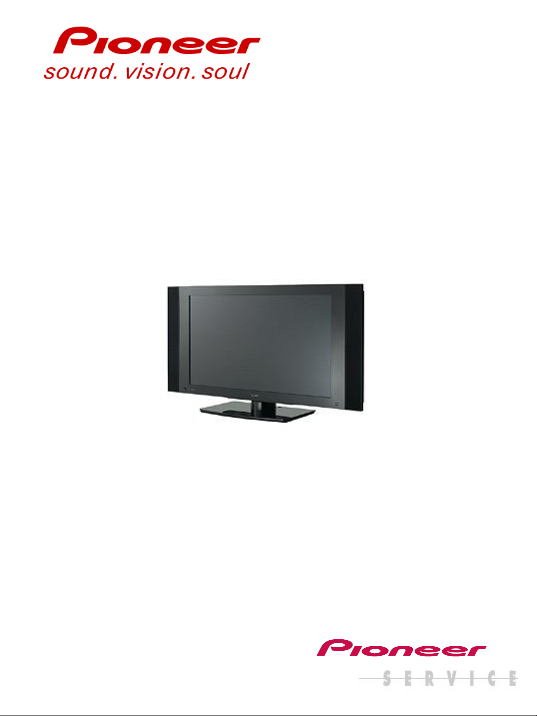
42 Inch Plasma Display
Training &
Trouble Shooting Guide
G-5
PDP-42A3HD
PDP-4214HD
Technical Training Department
1925 E. Dominguez Street
Long Beach, CA 90810
Page 2

Page 3

Contents
Controls and Connections……..…...4~7
Front View……………….……………….4
Rear View…………………………….…..5
Remote Control………..…………..…...6~7
Basic Block Diagrams………….……8~15
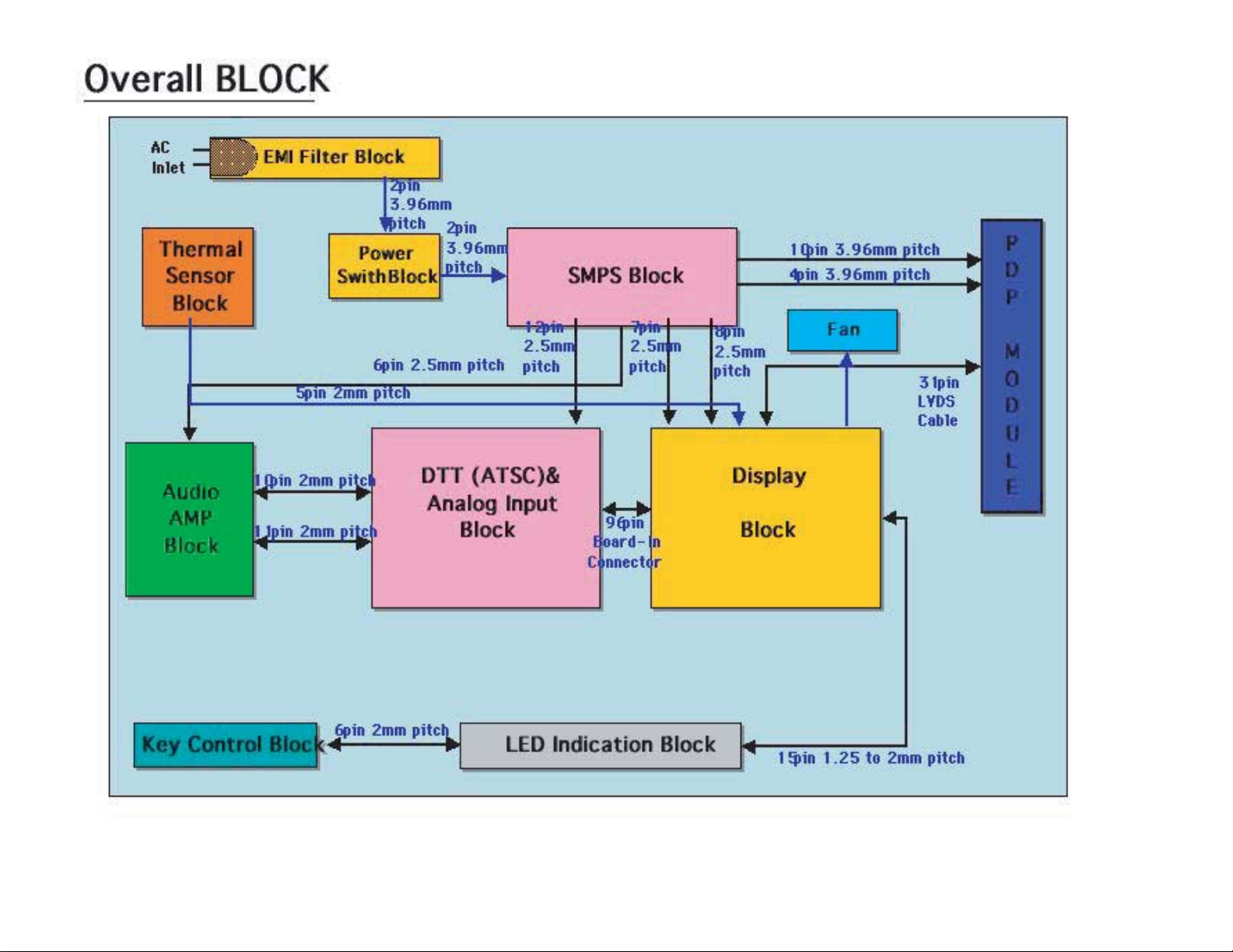
Overall Block Diagram…….....…………8
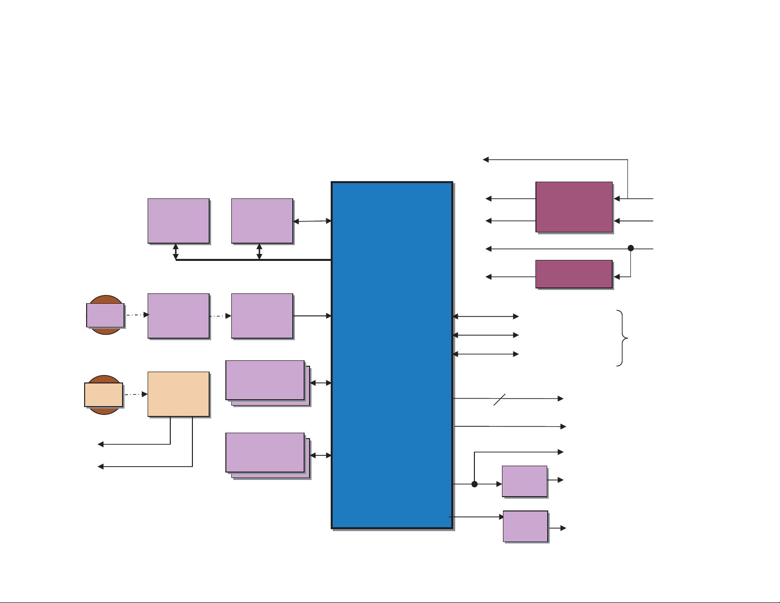
ATSC Tuner Tuner Block……….……...9
Digital Block……………………..….....10~11
DTT and Analog Block……..….…..…12~13
Display Block Description
& Factory Mode…………………….…14~15
Signal Flow Block Diagrams………16~28
Analog Tuner Input Main Flow……..…16
Analog Tuner Input Sub Block…….….17
Composite Input Main…………………18
Composite Input Sub…………………..19
S Input Main………………………….…20
S Input Sub……………………………..21
ATSC (HD Signal) Main……………….22
ATSC (HD Signal) Sub………………..23
Component Input Main………………..24
Component Input Sub…………………25
HDMI Input Main……………………….26
HDMI Input Sub………………………..27
Caption Input…………………………..28
Input and Tuner Board Locations……29
.
White Balance Adjustment.…….…...30
Power Down Tip………….…………..31
Troubleshooting (Tuner Module)...32~73
No Power………………………………32~33
No HDMI………………..………..…....34~35
No Component Signal………….…....36~37
No TV Signal………...………….…….38~39
No Video or No S Video Signal….….40~43
No Audio…………………………….…44~50
No Caption………………………….…52~53
No Remote Control Operation………54~55
No Key Control………………………..56~57
DTT Board Troubleshooting…………58~73
Disassembly………………………...…74~77
Troubleshooting (PDP Panel)….….78~99
Required Tools…………………….….78
Parts List (Boards & Versions)………79
Basic Troubleshooting Flow Chart.….81
Model & Serial Number Location….…82
Panel Crack Identification…………….82
Connectors and Cables……………...83~86
Vertical or Horizontal Lines………..…87
No Picture………………………….…..88~90
Abnormalities in the Picture……….…91
Power Off………………………………92~95
Detaching Connectors & Boards……96~99
Adjustments……………………….…100~101
Page 4
Plasma Display
DTV TV VCR DVD HDMI
STANDBY
4
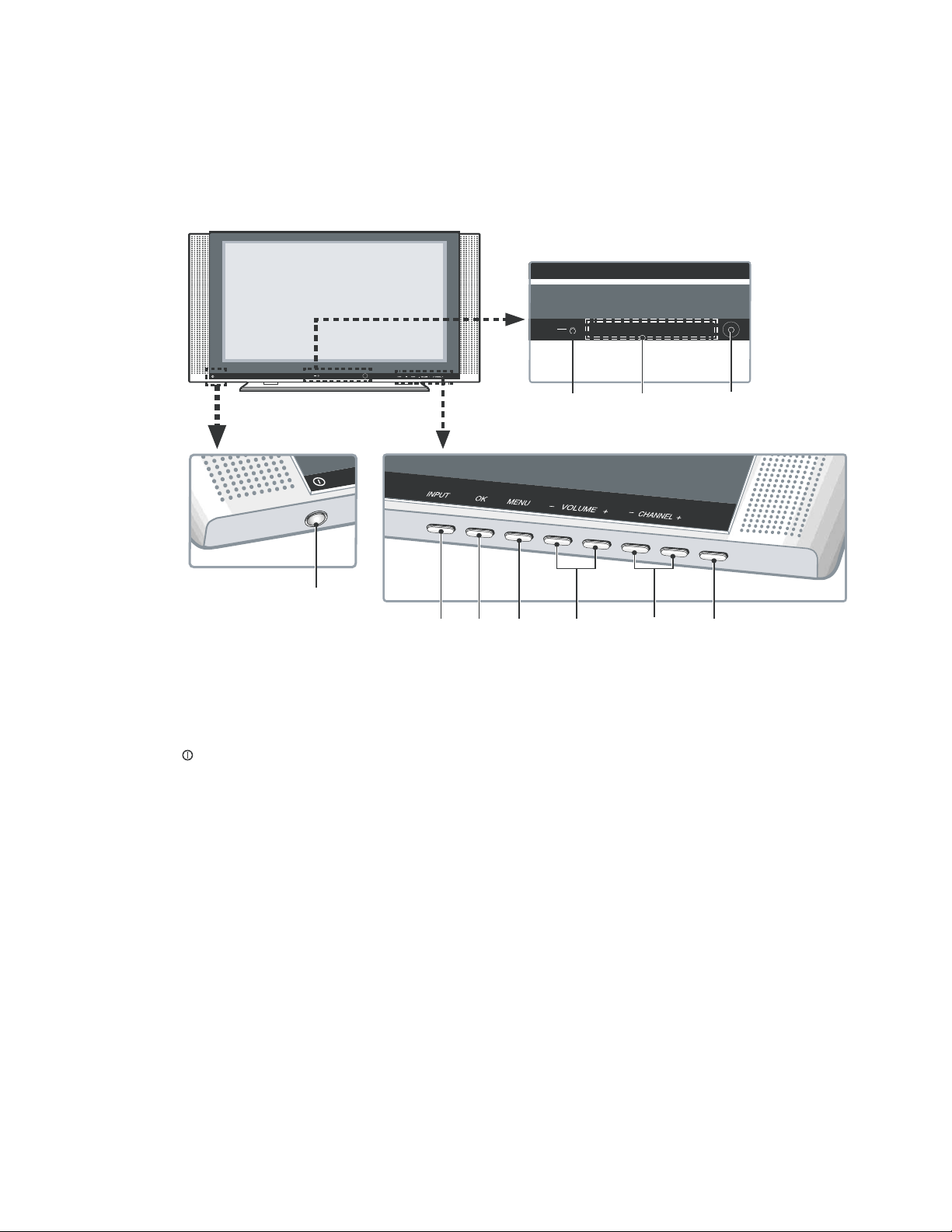
Front view
STANDBY
POWE R
DTV TV VCR DVD HDMI
WE
PO
R
1
1 POWER button
2STANDB Y indicator
3 Current input source indicators
4 Remote control sensor
5INPUT button
STANDBY
/ON
342
S
T
A
ND
B
Y
/O
N
5910
6
78
6OK button
7MENU button
8 VOLUME –/+ buttons
9 CHANNEL –/+ button s
10 ST ANDB Y/ON button
Page 5
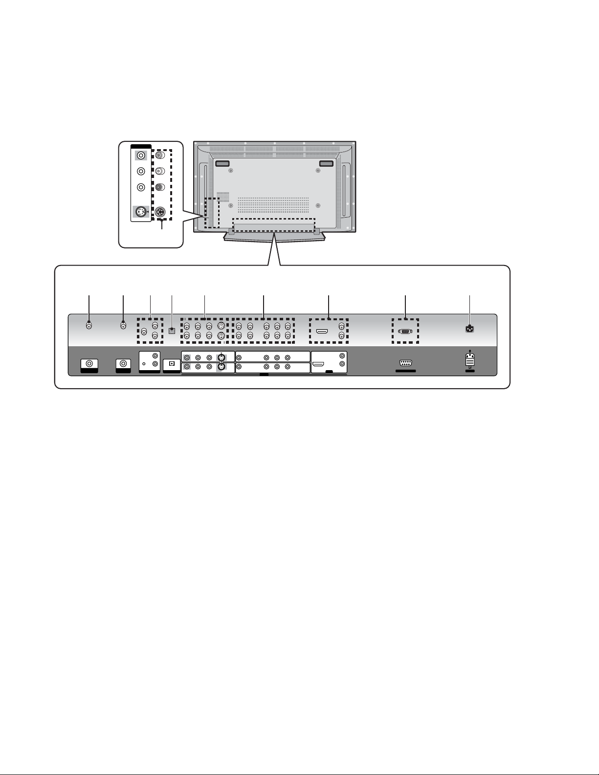
Rear view
5
INPUT
VIDEO 3
L
R
AUDIO
S-VIDEO 3
1
234 8 9
DTVANTENNA IN
ANTENNA
/ CABLE IN
VIDEO
MONITOR OUT
5
L
R
OPTICAL
AUDIO
DIGITAL OUT
6 7
VIDEO 2 L-AUDIO-R
VIDEO 1
L-AUDIO-R S-VIDEO 1
S-VIDEO 2
L-AUDIO-R Y
L-AUDIO-R Y
The terminals have faced downward.
1 VIDEO 3 terminals (AUDIO/VIDEO/S-VIDEO)
2 DTV-ANTENNA IN terminal
3 ANTENNA/CABLE IN terminal
4 MONITOR OUT terminals (AUDIO/VIDEO)
5 DIGITAL OUT terminal (OPTICAL)
6 VIDEO 1/VIDEO 2 terminals (AUDIO/VIDEO/
S-VIDEO)
10
CB/PB
CR/PR
COMPONENT 2
COMPONENT 1
CB/PB
CR/PR
INPUT
7 COMPONENT 1/COMPONENT 2 terminals
(COMPONENT VIDEO/AUDIO)
8 HDMI terminal (AUDIO/HDMI)
9 RS-232C terminal (service only)
10 AC IN terminal
L
R
AUDIOHDMI
HDMI
SERVICE ONLY AC IN
Page 6
Remote control unit
6
10
11
12
13
1
2
AV SELECTION
3
4
5
6
7
FAVORITE
8
9
CH
RETURN
HD WIDEINPUT
SCREEN SIZESOUND EFFECT
11 3322
44 6655
77 9988
00
C.C.
SLEEP
CH
OK
EXIT BACK
VOLCH
MUTING
SPLIT SPLIT P IN P SWAP
INPUT SHIFT
SPLIT SPLIT
CH+ CH–
DTV
SIGNAL MTS LIST
TV
CH
ENTER
DISPLAY
MENU
CH
DELETE
14
15
16
17
18
19
20
21
22
1
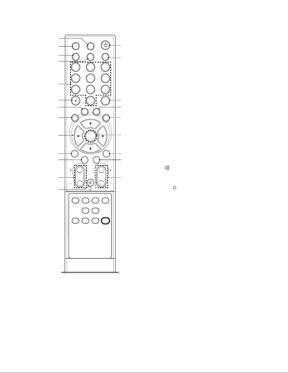
HD WIDE : Adjusts the picture to fit the 16:9
wide aspect ratio. Available in DTV mode.
2
INP UT : Displays all available input sources.
Press the
or \ button to select the required
\
input source.
3 AV SELECTION
: Selects the picture mode
(Standard, Dynamic, Movie, Game or User).
4
SOUND EFFECT : Selects the sound effect
(Flat, Speech, Movie, Music or User).
5
0-9 : Select the channel.
6
(dot): Selects the sub-channel of DTV.
7
C.C.: Display captions while in the closed-
caption source.
8 FAVORITE CH
9
/|/|/\: Controls the cursor in the on-
\
: Selects the favorite channel.
screen menu.
10
CH RETURN : Returns the selected channels.
11
EXIT : Exits from any display.
12 CH +/
13
–: Changes the channel.
MUTING: Mutes the sound. To turn the
sound back on, press the MUTING, VOL+ or
VOL – buttons.
14 TV
: Switches between operation and
standby mode.
15 S
CREEN SIZE: Changes the aspect ratio of
the screen (Zoom/Cinema/Full/4:3/Wide).
16 CH ENTE
17
SLEEP: Sets the sleep timer.
18
DISPL AY: Shows the display.
19 OK
20
: Executes a command.
MENU : Displays the on-screen menu .
21 BACK
22 VOL
R: Enters channels.
: Returns to the previous menu screen.
+/–:Sets the volume.
Page 7
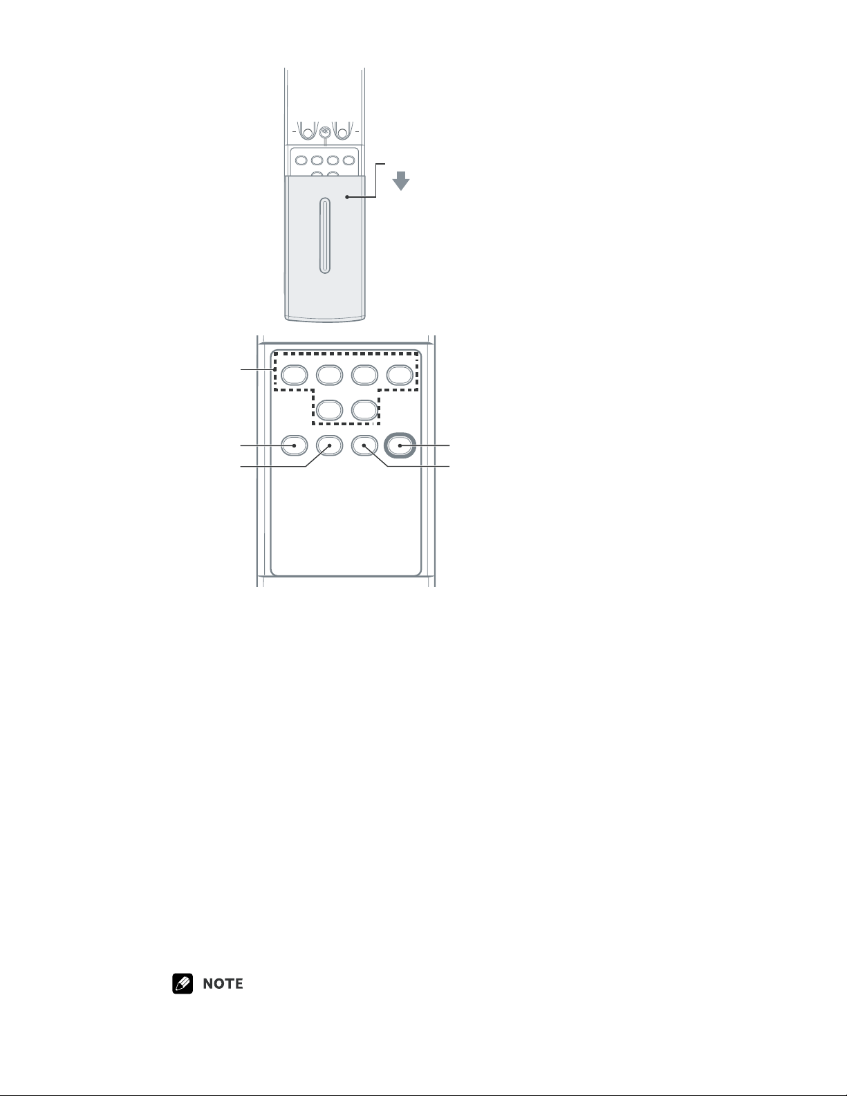
MUTING
VO LCH
7
SPLIT SPLIT P IN PSWAP
INPUT SHIFT
SPLIT SPLIT
CH+ C H–
MTS LIST
FAVORITE
CH DELETE
SIGNAL
DTV
Slid e
23
24
25
SPLIT SPLIT P IN PSWAP
INPUT SHIFT
SPLIT SPLIT
CH+ CH–
DTV
SIGNAL MTS LIST
CH
DELETE
26
27
23 SPLIT Function Buttons
SPLIT : Selects the SPLIT mode (Off, PIP, Twin1
or Twin2).
SPLIT INPUT : Selects an input source for the
sub picture.
P IN P/SHIFT : Selectsa position for the sub-
picture.
SWAP : Interchanges the main picture and
sub-picture.
SPLIT CH +, SPLIT CH – : Changes the
channel of the sub-picture.
24 DTV SIGNAL : Displays the signal strength
and quality.
25 MTS : Selects the sound mode .
26 CH DELETE: Deletes a channel in Edit Chan-
nel List.
27 LIST : Displays the channel list. Press the
button to select the required channel.
|
|
or
•When using the remote control unit, point it at the Plasma Display.
Page 8
8
(Power Supply)
(Tuner Block Analog & HDTV)
(Main CPU)
(RGB Block)
(Front Panel LED's)
Page 9
+3.3V
ATS
/PDIF
9
ATSC Block
Operating System
Customer Settings
CPU & MPEG Decoder
(480I Out)
ATSC = Advanced Television Systems Committee (Digital Television Standards)
NTSC = National Television System Committee (Analog Television Standards)
ATSC
ATSC
Jack Ant
NTSC
NTSC
CVBS NTSC
SIF_A
EEPROM
16KB
Digital
Tuner
Analog
Tuner
Flash
4MByte
Channel
Decoder
DDR SDRM
32MByte
DDR SDRM
32MByte
CPU
MDIN
MDIN
150
(TL955B2-SH)
150
+2.5V
+1.2V
+5.0V
+2.5V
+1.2V
3
. DC-DC
Converter
Linear Reg.
UART0 (Commu nication)
UART1 (RS232C)
UART2 (RS232C)
For Deb ug
ATSC YPbPr Out
(720P/108 0i)
ATSC CVBS Out
IIS (ATSC)
Audio
Audio
DAC
DAC
L/R ATSC
+3.3V
+A6VCC
+2.5V
Communication
To Disp lay Board
ATS
C S/PDIF
Digital-
Digital-
SW
SW
S/PDIF Out
Page 10
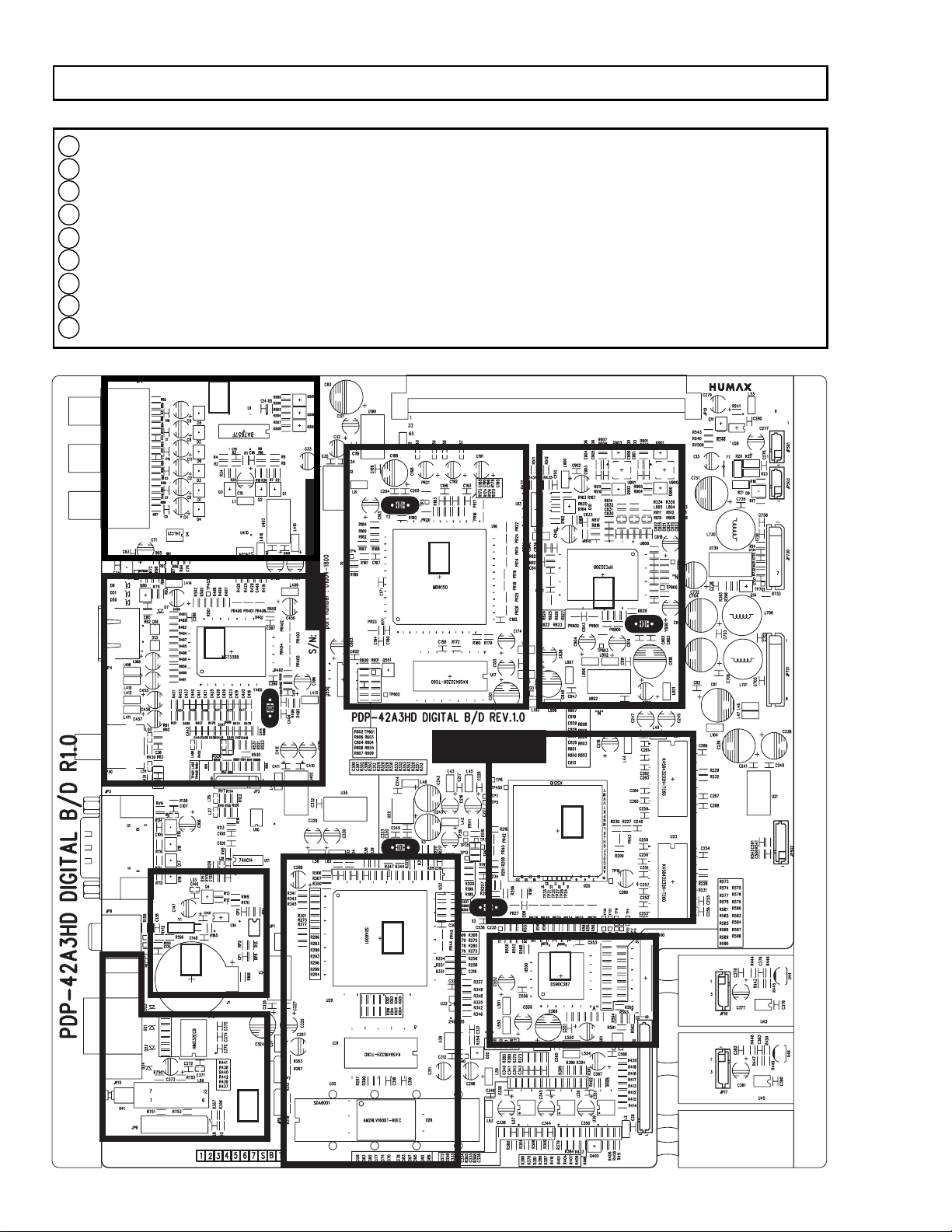
1. Digital PCB Block
10
F
E
A : Component Video input Block(BA7657)
B : ADC and HDMI receiver Block(MST3388M)
C : Real Timer Block(M41T81)
D : RS232 communication part
E : Micom Block(SDA6001+K4S641632H-TC60+AM29LV160DT)
F : Deinterlace Block(MDIN150+K4S643232H-TC60)
G : Sub-Video Decoder Block(VPC3230)
H : Scaler Block(ASI510)
I : LVDS transmitter Block(DS90C387)
A
C
G
B
H
I
D
Page 11

Block Description of DTT
11
1. DC-DC Block is composed of Regulators(BA05(5V), LP3965ES(1.2V), LP2995MX(VREF,VTT)) and
SMPS powers(2V5VCC,3V3VCC,A6VCC).
2. UART Communication is composed of UART1(Communication), UART2(RS232), UART3(RS232 for
debug)
3. The EEPROM block stores the current states, channels, and other user setting values.
4. The Flash Rom block stores operation source.
5. ATSC input block is composed of Digital tuner(DTT7608) and channel Decorder(LGDT3303).
6. NTSC input block is composed of Analog Tuner and connects in Video decorder(uPD64012).
7. DDR SDRAM block is composed of 4 32MByte and stores the current Video and information
instantly.
8. The CPU block functions MPEG decoder, converts the video format and controls the related IC's.
9. The Audio DAC converts from IIC Audio to L/R Analog Audio.
10. The SPDIF outputs 5.1Ch Dolby Digital audio signal.
Page 12
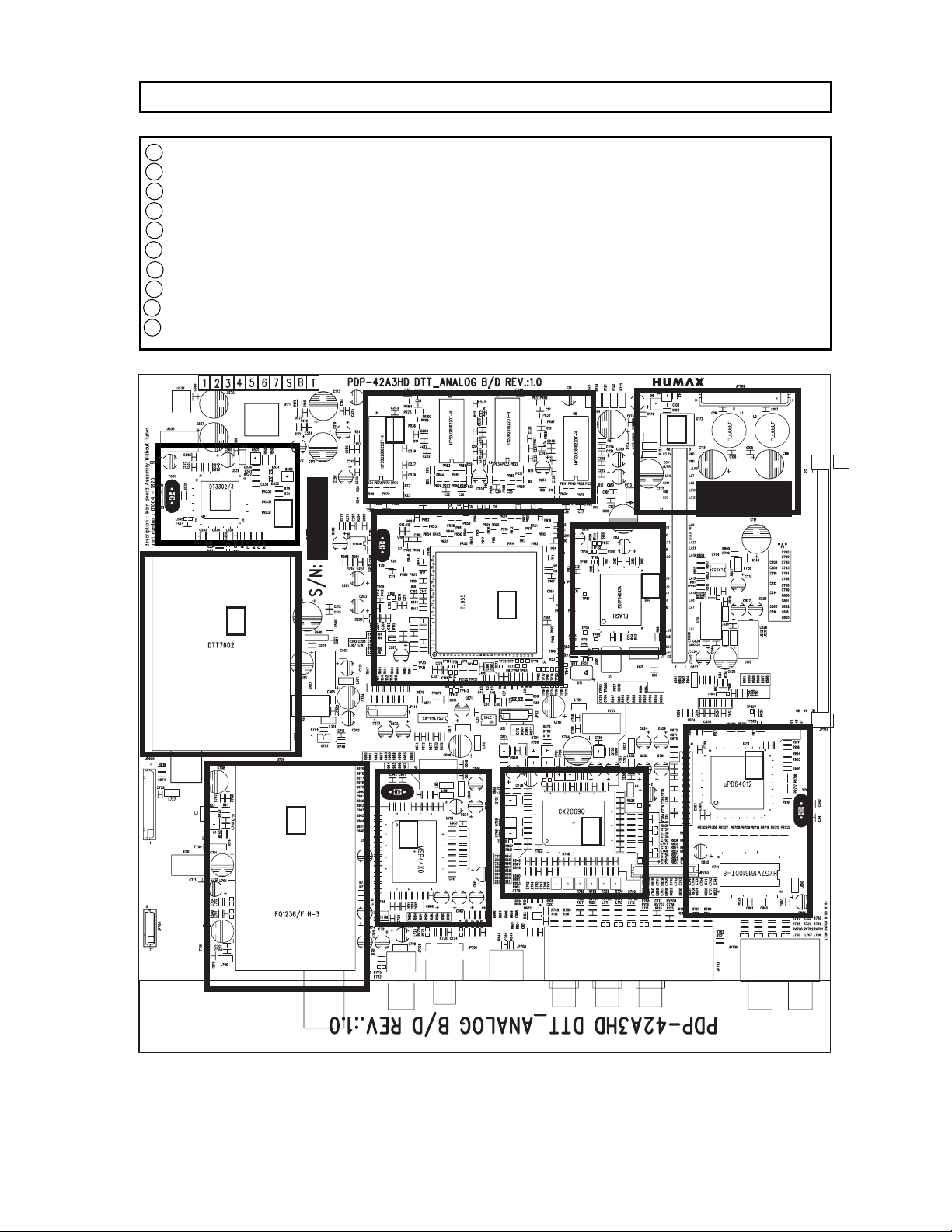
2. DTT & Analog PCB Block
12
I
H
A : Channel Demodulator Block(LGDT3303)
B : ATSC Tuner Block(DTT7608)
C : Analog Tuner Block(FQ1236)
D : DDR SDRAM Block(HY5DU281622ET-H x 4)
E : MPEG Decoder Block(TL955B2-SH)
F : Audio Decoder Block(MSP4440)
G : Video Switch Block(CX2069Q)
H : Flash Rom Block(E28F320J3A)
I : Power input Block
J : Main Video decoder Block(uPD64012+HY57V161610DTC-7)
D
A
E
B
J
C
F
G
Page 13
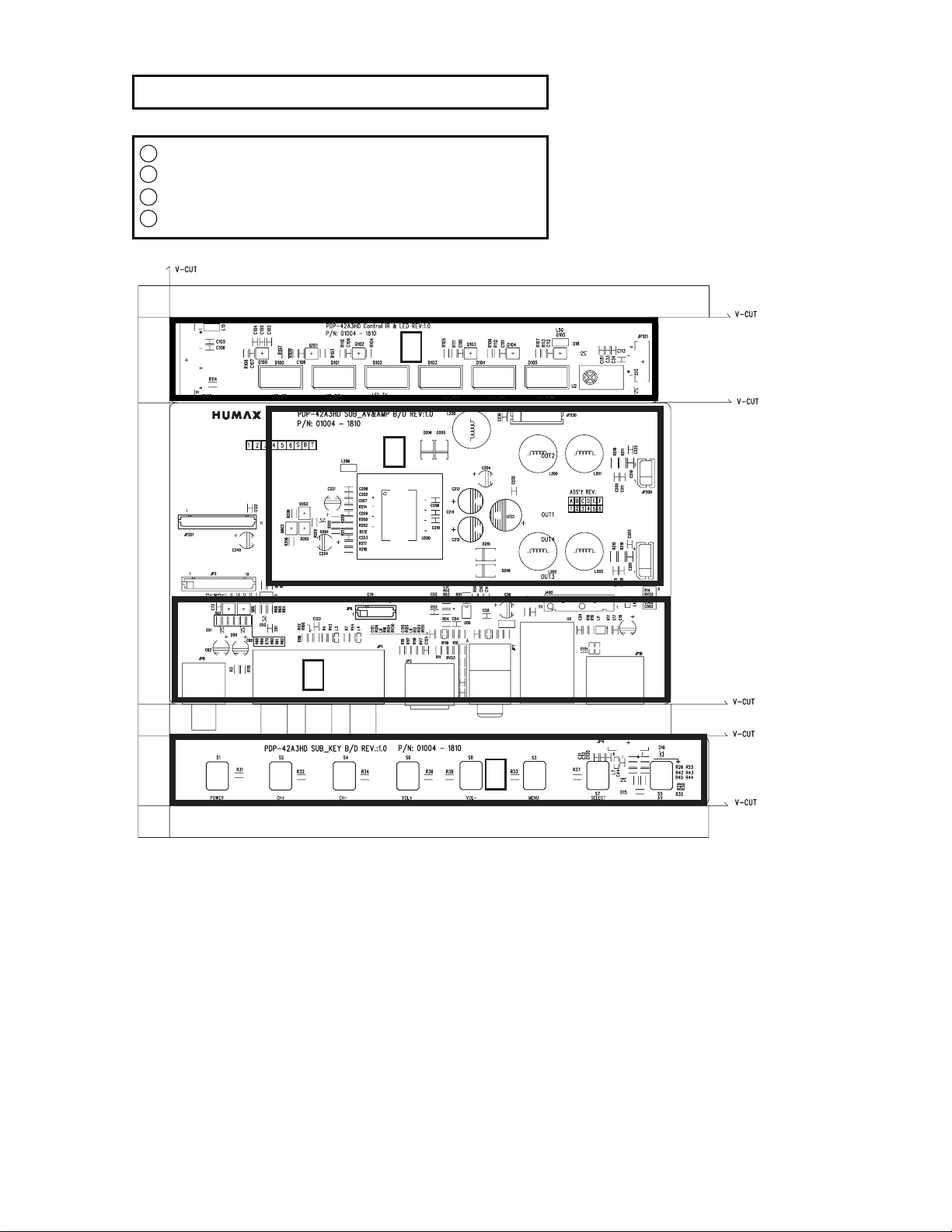
3. Digital PCB Block
13
A : Indication LED Block
B : Audio AMP Block(TA2024B)
C : AV input Block
D : Control key Block
A
B
C
D
Page 14

Block Description of Display
14
Normally no adjustments are required to this product, even after
a repair or PCB has been changed.
1. The ADC & HDMI receiver used on this board (MST3388-110).
2. The Video Decoder is composed of uPD64012 and VPC3230, converts from analog signal to
digital video signal. UPD64012 is used for 480I sub picture only.
3. The CXA2069 switches input signal and selects the signal. Analog Only (Tuner,YC and composite).
4. The MDIN150 is de-interlacer, it functions that interlaced signal converts de-interlaced signal and
improves picture quality. (I/P Converter)
5. The ASI510 is scaler IC, scaling video signal it interfaces with related IC and outputs 24 bit RGB
format video.
The SDA6001 is composed of micom and closed caption block, it controls related IC, power on/off
6.
system, and signal flowing system.
7. IO expander functions that it increases the IO port from receiving IIC communication signal.
8. The real timer(M41T81) is timer with using the clock generator.
Factory Mode
1. •To enter the test mode press keys on remote control in sequence as below.
TV/AV 0 9 1 7
•You can make adjustments, but proper settings are very critical for set operations
.
2. Self-check mode and error code is not applicable in this set.
Page 15
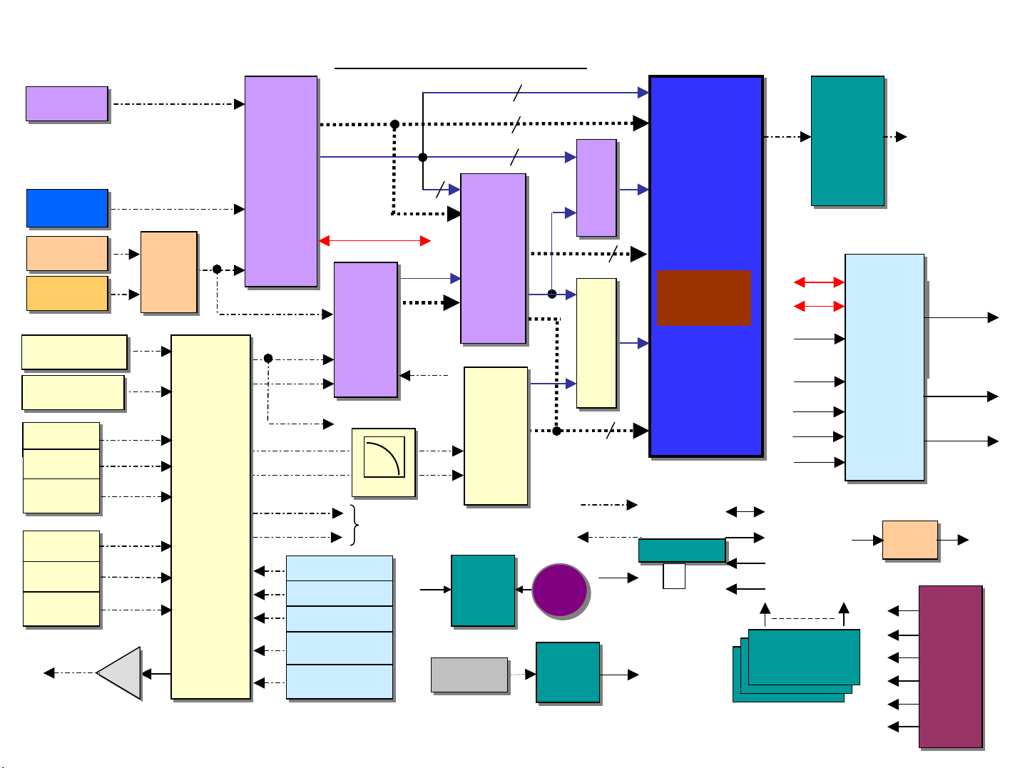
Display BLOCK
15
HDMI
HDMI
ATSC
ATSC
YPbPr 1
YPbPr 1
YPbPr 2
YPbPr 2
NTSC_CVBS
NTSC_CVBS
ATSC_CVBS
ATSC_CVBS
CVBS 1
CVBS 1
CVBS 2
CVBS 2
CVBS 3
CVBS 3
Y/C 1
Y/C 1
Y/C 2
Y/C 2
Y/C 3
Y/C 3
CVBS & Audio
LINE_OUT
BA7657
7657
7657
CXA2069
(A_S/W)
9886
9886
MST3388
-110
~ 480P
CVBS1
Y1/C1
MICOM_CVBS
CVBS2/Y2
C2
Audio L-Main
Audio R-Main
RGB
HDMI I2S & S/PDIF
uPD
64012
(Video
Decode,
C/C & 3D)
To MSP
L/R SC2
L/R SC2
L/R CVBS1
L/R CVBS1
L/R CVBS2
L/R CVBS2
L/R CVBS3
L/R CVBS3
L/R DVI
L/R DVI
LPF
RGB/FB
For CC
5Vst
MDIN
(I/P)
VPC3230
(Decode)
Real
Real
Timer
Timer
(M41T81)
(M41T81)
RS232C
RS232C
150
24
4
5
8 Bit
MUX
24
8 Bit
MUX
16
MICOM_CVBS
RGB/FB
IIC
Bat.
Bat.
232C
MAX232
MAX232
Rx/Tx
Rx/Tx
D-H/V Sync & clk
A-INE[23:0]
A-H/V Sync & clk
MDIN
MDIN
150
D-INO[23:0]
150
ASI510
(Scaler)
V-H/V Sync & clk
V-IN [15:0]
SDA6000M
Tele-text
C/C
4
IIC
LED
Key
I/R
30
HDMI I2S
ATSC I2S
SIF _A
L/R Main
(CXA2069)
L/R ATSC
L/R DTV1
L/R DTV2
From
MSP4440
Output
I/O
Expender
(~DE)
J-
J-
LVDS Tx
L003
L003
DS90C387
(~SOG)
Audio
Audio
(2069,
(2069,
MSP44X0,
MSP44X0,
4052)
Audio
4052)
MSP44X0
P
MAX232
MAX232
Amp
Amp
. M7V
. A6VCC
. A12VCC
. 12VCC
. 2V5VCC
. 3V3VCC
L/R SC2
(CXA2069)
L/R Aux.
(Headphone)
L/R Main
(Power Amp)
Speaker
Page 16
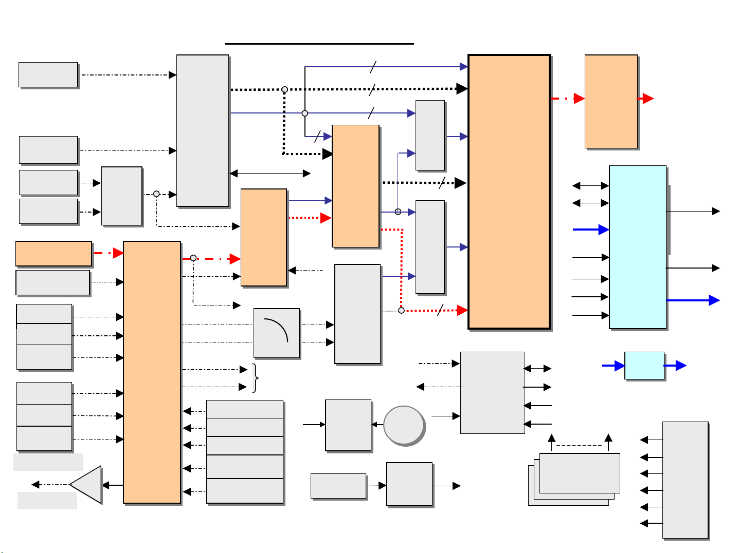
ATV Input(Main)
16
HDMI
HDMI
ATSC
ATSC
YPbPr 1
YPbPr 1
YPbPr 2
YPbPr 2
NTSC_CVBS
NTSC_CVBS
ATSC_CVBS
ATSC_CVBS
CVBS 1
CVBS 1
CVBS 2
CVBS 2
CVBS 3
CVBS 3
Y/C 1
Y/C 1
Y/C 2
Y/C 2
Y/C 3
Y/C 3
CVBS & Audio
LINE_OUT
BA7657
7657
7657
CXA2069
(A_S/W)
MST3388
-110
~ 480P
CVBS1
Y1/C1
MICOM_CVBS
CVBS2/Y2
C2
Audio L-Main
Audio R-Main
L/R CVBS1
L/R CVBS2
L/R CVBS3
RGB
HDMI I2S & S/PDIF
uPD
64012
(Video
Decode,
C/C & 3D)
To MSP
L/R SC2
L/R SC2
L/R CVBS1
L/R CVBS2
L/R CVBS3
L/R DVI
L/R DVI
LPF
RGB/FB
For CC
5Vst
MDIN
(I/P)
VPC3230
(Decoder)
Real
Real
Timer
Timer
(M41T81)
(M41T81)
RS232C
RS232C
150
24
4
5
8 Bit
MUX
24
8 Bit
MUX
16
D-H/V Sync & clk
A-INE[23:0]
MDIN
MDIN
150
150
4
A-H/V Sync & clk
D-INO[23:0]
ASI510
(Scaler)
V-H/V Sync & clk
V-IN [15:0]
30
(~SOG)
HDMI I2S
ATSC I2S
SIF _A
L/R Main
(CXA2069)
L/R ATSC
L/R DTV1
L/R DTV2
(~DE)
J-
J-
LVDS Tx
L003
L003
DS90C387
MSP44X0
Audio
Audio
(2069,
(2069,
MSP44X0,
MSP44X0,
4052)
Audio
4052)
Panel
L/R SC2
(CXA2069)
L/R Aux.
(Headphone)
L/R Main
(Power Amp)
From
IIC
MICOM_CVBS
RGB/FB
Bat.
Bat.
232C
MAX232
MAX232
Rx/Tx
Rx/Tx
SDA6001
Tele-text
C/C
IIC
LED
Key
I/R
MSP4440
Output
I/O
Expender
MAX232
MAX232
Amp
Amp
Speaker
. M7V
. A6VCC
. A12VCC
. 12VCC
. 2V5VCC
. 3V3VCC
Page 17
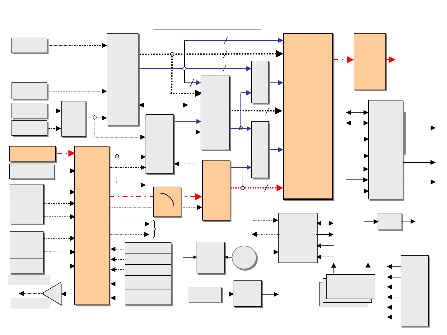
ATV Input(Sub)
17
HDMI
HDMI
ATSC
ATSC
YPbPr 1
YPbPr 1
YPbPr 2
YPbPr 2
NTSC_CVBS
NTSC_CVBS
ATSC_CVBS
ATSC_CVBS
CVBS 1
CVBS 1
CVBS 2
CVBS 2
CVBS 3
CVBS 3
Y/C 1
Y/C 1
Y/C 2
Y/C 2
Y/C 3
Y/C 3
CVBS & Audio
LINE_OUT
BA7657
7657
7657
CXA2069
(A_S/W)
MST3388
-110
~ 480P
CVBS1
Y1/C1
MICOM_CVBS
CVBS2/Y2
C2
Audio L-Main
Audio R-Main
L/R CVBS1
L/R CVBS2
L/R CVBS3
RGB
HDMI I2S & S/PDIF
uPD
64012
(Video
Decode,
C/C & 3D)
To MSP
L/R SC2
L/R SC2
L/R CVBS1
L/R CVBS2
L/R CVBS3
L/R DVI
L/R DVI
LPF
RGB/FB
For CC
5Vst
MDIN
(I/P)
VPC3230
(Decoder)
Real
Real
Timer
Timer
(M41T81)
(M41T81)
RS232C
RS232C
150
24
4
5
8 Bit
MUX
24
8 Bit
MUX
16
D-H/V Sync & clk
A-INE[23:0]
A-H/V Sync & clk
MDIN
MDIN
150
D-INO[23:0]
150
ASI510
(Scaler)
V-H/V Sync & clk
V-IN [15:0]
4
30
HDMI I2S
ATSC I2S
SIF _A
L/R Main
(CXA2069)
L/R ATSC
L/R DTV1
L/R DTV2
(~DE)
J-
J-
LVDS Tx
L003
L003
DS90C387
(~SOG)
Audio
Audio
(2069,
(2069,
MSP44X0,
MSP44X0,
4052)
Audio
4052)
MSP44X0
Panel
L/R SC2
(CXA2069)
L/R Aux.
(Headphone)
L/R Main
(Power Amp)
From
IIC
MICOM_CVBS
RGB/FB
Bat.
Bat.
232C
MAX232
MAX232
Rx/Tx
Rx/Tx
SDA6000M
Tele-text
C/C
IIC
LED
Key
I/R
MSP4440
Output
I/O
Expender
MAX232
MAX232
Amp
Amp
Speaker
. M7V
. A6VCC
. A12VCC
. 12VCC
. 2V5VCC
. 3V3VCC
Page 18
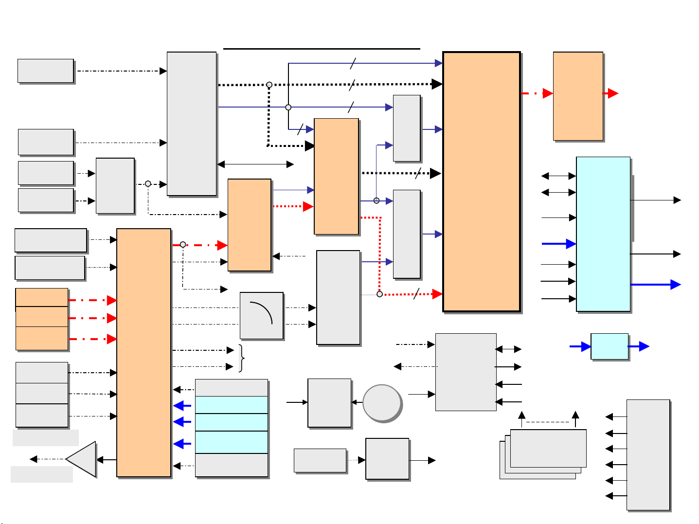
CVBS Input(Main)
18
HDMI
HDMI
ATSC
ATSC
YPbPr 1
YPbPr 1
YPbPr 2
YPbPr 2
NTSC_CVBS
NTSC_CVBS
ATSC_CVBS
ATSC_CVBS
CVBS 1
CVBS 1
CVBS 2
CVBS 2
CVBS 3
CVBS 3
Y/C 1
Y/C 1
Y/C 2
Y/C 2
Y/C 3
Y/C 3
CVBS & Audio
LINE_OUT
BA7657
7657
7657
CXA2069
(A_S/W)
MST3388
-110
~ 480P
CVBS1
Y1/C1
MICOM_CVBS
CVBS2/Y2
C2
Audio L-Main
Audio R-Main
L/R CVBS1
L/R CVBS2
L/R CVBS3
RGB
HDMI I2S & S/PDIF
uPD
64012
(Video
Decode,
C/C & 3D)
To MSP
L/R SC2
L/R SC2
L/R CVBS1
L/R CVBS2
L/R CVBS3
L/R DVI
L/R DVI
LPF
RGB/FB
For CC
5Vst
MDIN
(I/P)
VPC3230
(Decoder)
Real
Real
Timer
Timer
(M41T81)
(M41T81)
RS232C
RS232C
150
24
4
5
8 Bit
MUX
24
8 Bit
MUX
16
D-H/V Sync & clk
A-INE[23:0]
A-H/V Sync & clk
MDIN
MDIN
150
D-INO[23:0]
150
ASI510
(Scaler)
V-H/V Sync & clk
V-IN [15:0]
(~DE)
30
4
HDMI I2S
ATSC I2S
SIF _A
L/R Main
(CXA2069)
L/R ATSC
L/R DTV1
L/R DTV2
J-
J-
LVDS Tx
L003
L003
DS90C387
(~SOG)
Audio
Audio
(2069,
(2069,
MSP44X0,
MSP44X0,
4052)
Audio
4052)
MSP44X0
Panel
L/R SC2
(CXA2069)
L/R Aux.
(Headphone)
L/R Main
(Power Amp)
From
IIC
MICOM_CVBS
RGB/FB
Bat.
Bat.
232C
MAX232
MAX232
Rx/Tx
Rx/Tx
SDA6000M
Tele-text
C/C
IIC
LED
Key
I/R
MSP4440
Output
I/O
Expender
MAX232
MAX232
Amp
Amp
Speaker
. M7V
. A6VCC
. A12VCC
. 12VCC
. 2V5VCC
. 3V3VCC
Page 19
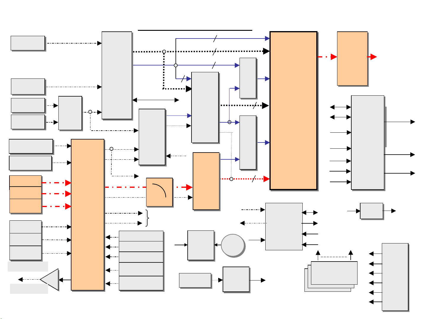
CVBS Input(Sub)
19
HDMI
HDMI
ATSC
ATSC
YPbPr 1
YPbPr 1
YPbPr 2
YPbPr 2
NTSC_CVBS
NTSC_CVBS
ATSC_CVBS
ATSC_CVBS
CVBS 1
CVBS 1
CVBS 2
CVBS 2
CVBS 3
CVBS 3
Y/C 1
Y/C 1
Y/C 2
Y/C 2
Y/C 3
Y/C 3
CVBS & Audio
LINE_OUT
BA7657
7657
7657
CXA2069
(A_S/W)
MST3388
-110
~ 480P
CVBS1
Y1/C1
MICOM_CVBS
CVBS2/Y2
C2
Audio L-Main
Audio R-Main
L/R CVBS1
L/R CVBS2
L/R CVBS3
RGB
HDMI I2S & S/PDIF
uPD
64012
(Video
Decode,
C/C & 3D)
To MSP
L/R SC2
L/R SC2
L/R CVBS1
L/R CVBS2
L/R CVBS3
L/R DVI
L/R DVI
LPF
RGB/FB
For CC
5Vst
MDIN
(I/P)
VPC3230
(Decoder)
Real
Real
Timer
Timer
(M41T81)
(M41T81)
RS232C
RS232C
150
24
4
5
8 Bit
MUX
24
8 Bit
MUX
16
D-H/V Sync & clk
A-INE[23:0]
A-H/V Sync & clk
MDIN
MDIN
150
D-INO[23:0]
150
ASI510
(Scaler)
V-H/V Sync & clk
V-IN [15:0]
(~DE)
30
4
HDMI I2S
ATSC I2S
SIF _A
L/R Main
(CXA2069)
L/R ATSC
L/R DTV1
L/R DTV2
J-
J-
LVDS Tx
L003
L003
DS90C387
(~SOG)
Audio
Audio
(2069,
(2069,
MSP44X0,
MSP44X0,
4052)
Audio
4052)
MSP44X0
Panel
L/R SC2
(CXA2069)
L/R Aux.
(Headphone)
L/R Main
(Power Amp)
From
IIC
MICOM_CVBS
RGB/FB
Bat.
Bat.
232C
MAX232
MAX232
Rx/Tx
Rx/Tx
SDA6000M
Tele-text
C/C
IIC
LED
Key
I/R
MSP4440
Output
I/O
Expender
MAX232
MAX232
Amp
Amp
Speaker
. M7V
. A6VCC
. A12VCC
. 12VCC
. 2V5VCC
. 3V3VCC
Page 20
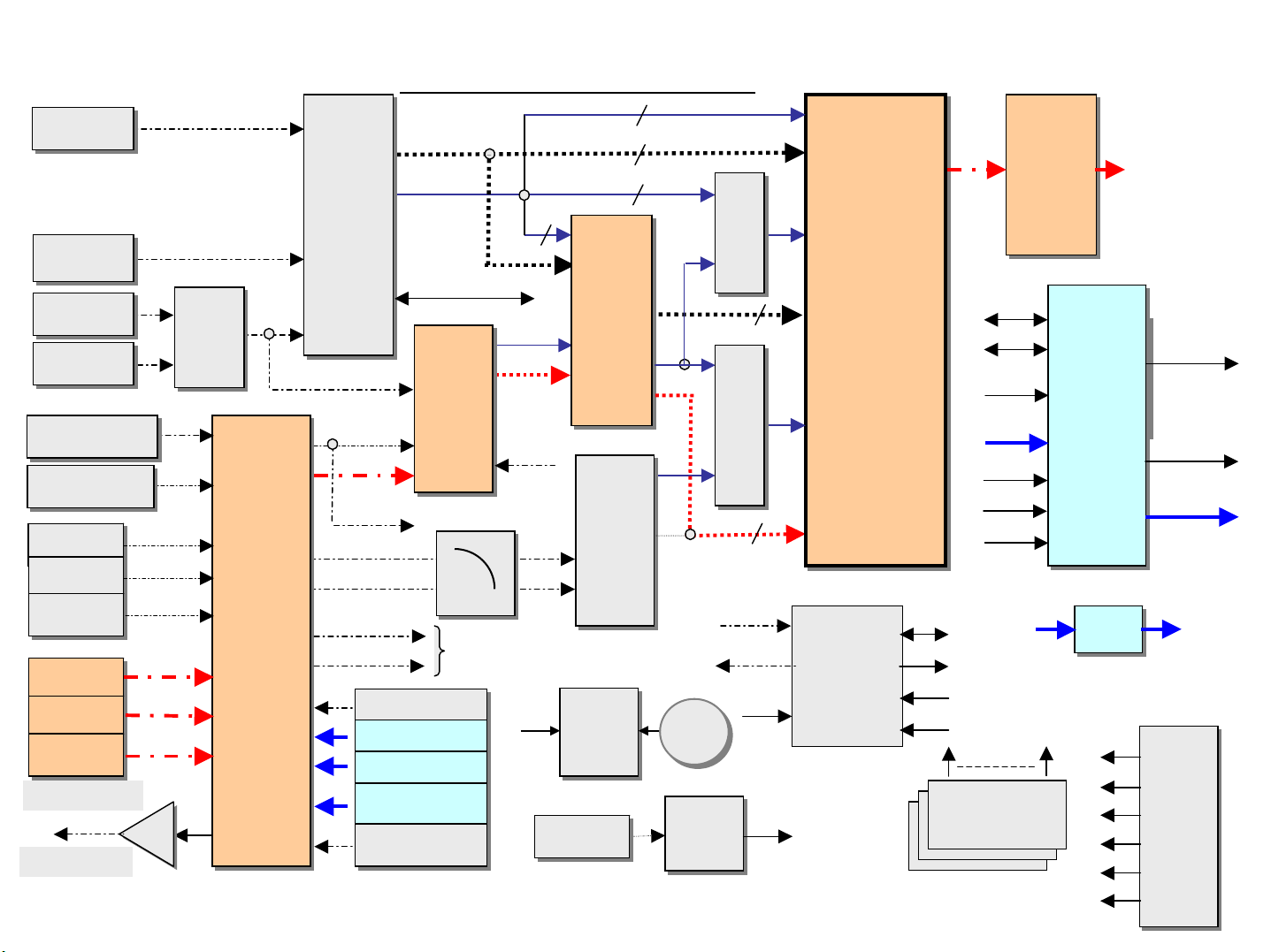
HDMI
20
HDMI
ATSC
ATSC
YPbPr 1
YPbPr 1
YPbPr 2
YPbPr 2
NTSC_CVBS
NTSC_CVBS
ATSC_CVBS
ATSC_CVBS
CVBS 1
CVBS 1
CVBS 2
CVBS 2
CVBS 3
CVBS 3
Y/C 1
Y/C 1
Y/C 2
Y/C 2
Y/C 3
Y/C 3
CVBS & Audio
LINE_OUT
BA7657
7657
7657
CXA2069
(A_S/W)
MST3388
-110
~ 480P
CVBS1
Y1/C1
MICOM_CVBS
CVBS2/Y2
C2
Audio L-Main
Audio R-Main
L/R CVBS1
L/R CVBS2
L/R CVBS3
S Input(Main)
RGB
HDMI I2S & S/PDIF
uPD
64012
(Video
Decode,
C/C & 3D)
To MSP
L/R SC2
L/R SC2
L/R CVBS1
L/R CVBS2
L/R CVBS3
L/R DVI
L/R DVI
RGB/FB
For CC
LPF
5Vst
MDIN
(I/P)
VPC3230
(Decoder)
Real
Real
Timer
Timer
(M41T81)
(M41T81)
RS232C
RS232C
150
24
4
5
8 Bit
MUX
24
8 Bit
MUX
16
D-H/V Sync & clk
A-INE[23:0]
A-H/V Sync & clk
D-INO[23:0]
MDIN
MDIN
150
150
4
ASI510
(Scaler)
V-H/V Sync & clk
V-IN [15:0]
30
HDMI I2S
ATSC I2S
SIF _A
L/R Main
(CXA2069)
L/R ATSC
L/R DTV1
L/R DTV2
(~DE)
J-
J-
LVDS Tx
L003
L003
DS90C387
(~SOG)
MSP44X0
Panel
Audio
Audio
(2069,
(2069,
MSP44X0,
MSP44X0,
4052)
Audio
4052)
L/R SC2
(CXA2069)
L/R Aux.
(Headphone)
L/R Main
(Power Amp)
From
IIC
MICOM_CVBS
RGB/FB
Bat.
Bat.
232C
MAX232
MAX232
Rx/Tx
Rx/Tx
SDA6000M
Tele-text
C/C
IIC
LED
Key
I/R
MSP4440
Output
I/O
Expender
MAX232
MAX232
Amp
Amp
Speaker
. M7V
. A6VCC
. A12VCC
. 12VCC
. 2V5VCC
. 3V3VCC
Page 21
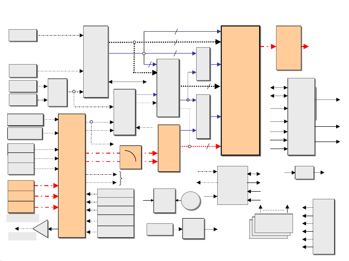
S Input(Sub)
21
HDMI
HDMI
ATSC
ATSC
YPbPr 1
YPbPr 1
YPbPr 2
YPbPr 2
NTSC_CVBS
NTSC_CVBS
ATSC_CVBS
ATSC_CVBS
CVBS 1
CVBS 1
CVBS 2
CVBS 2
CVBS 3
CVBS 3
Y/C 1
Y/C 1
Y/C 2
Y/C 2
Y/C 3
Y/C 3
CVBS & Audio
LINE_OUT
BA7657
7657
7657
CXA2069
(A_S/W)
MST3388
-110
~ 480P
CVBS1
Y1/C1
MICOM_CVBS
CVBS2/Y2
C2
Audio L-Main
Audio R-Main
L/R CVBS1
L/R CVBS2
L/R CVBS3
RGB
HDMI I2S & S/PDIF
uPD
64012
(Video
Decode,
C/C & 3D)
To MSP
L/R SC2
L/R SC2
L/R CVBS1
L/R CVBS2
L/R CVBS3
L/R DVI
L/R DVI
LPF
RGB/FB
For CC
5Vst
MDIN
(I/P)
VPC3230
(Decoder)
Real
Real
Timer
Timer
(M41T81)
(M41T81)
RS232C
RS232C
150
24
4
5
8 Bit
MUX
24
8 Bit
MUX
16
D-H/V Sync & clk
A-INE[23:0]
A-H/V Sync & clk
MDIN
MDIN
150
D-INO[23:0]
150
ASI510
(Scaler)
V-H/V Sync & clk
V-IN [15:0]
(~DE)
30
4
HDMI I2S
ATSC I2S
SIF _A
L/R Main
(CXA2069)
L/R ATSC
L/R DTV1
L/R DTV2
J-
J-
LVDS Tx
L003
L003
DS90C387
(~SOG)
Audio
Audio
(2069,
(2069,
MSP44X0,
MSP44X0,
4052)
Audio
4052)
MSP44X0
Panel
L/R SC2
(CXA2069)
L/R Aux.
(Headphone)
L/R Main
(Power Amp)
From
IIC
MICOM_CVBS
RGB/FB
Bat.
Bat.
232C
MAX232
MAX232
Rx/Tx
Rx/Tx
SDA6000M
Tele-text
C/C
IIC
LED
Key
I/R
MSP4440
Output
I/O
Expender
MAX232
MAX232
Amp
Amp
Speaker
. M7V
. A6VCC
. A12VCC
. 12VCC
. 2V5VCC
. 3V3VCC
Page 22
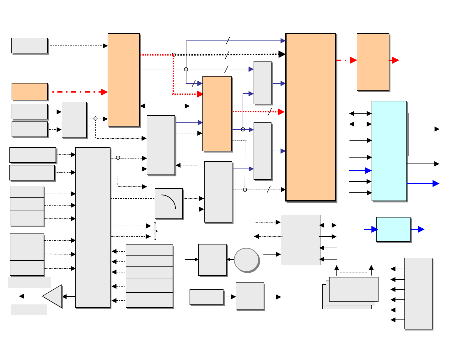
ATSC Input(Main)
22
HDMI
HDMI
ATSC
ATSC
YPbPr 1
YPbPr 1
YPbPr 2
YPbPr 2
NTSC_CVBS
NTSC_CVBS
ATSC_CVBS
ATSC_CVBS
CVBS 1
CVBS 1
CVBS 2
CVBS 2
CVBS 3
CVBS 3
Y/C 1
Y/C 1
Y/C 2
Y/C 2
Y/C 3
Y/C 3
CVBS & Audio
LINE_OUT
BA7657
7657
7657
CXA2069
(A_S/W)
MST3388
-110
~ 480P
CVBS1
Y1/C1
MICOM_CVBS
CVBS2/Y2
C2
Audio L-Main
Audio R-Main
L/R CVBS1
L/R CVBS2
L/R CVBS3
RGB
HDMI I2S & S/PDIF
uPD
64012
(Video
Decode,
C/C & 3D)
To MSP
L/R SC2
L/R SC2
L/R CVBS1
L/R CVBS2
L/R CVBS3
L/R DVI
L/R DVI
LPF
RGB/FB
For CC
5Vst
MDIN
(I/P)
VPC3230
(Decoder)
Real
Real
Timer
Timer
(M41T81)
(M41T81)
RS232C
RS232C
150
24
4
5
8 Bit
MUX
24
8 Bit
MUX
16
D-H/V Sync & clk
A-INE[23:0]
A-H/V Sync & clk
D-INO[23:0]
MDIN
MDIN
150
150
4
ASI510
(Scaler)
V-H/V Sync & clk
V-IN [15:0]
30
HDMI I2S
ATSC I2S
SIF _A
L/R Main
(CXA2069)
L/R ATSC
L/R DTV1
L/R DTV2
(~DE)
J-
J-
LVDS Tx
L003
L003
DS90C387
(~SOG)
MSP44X0
Audio
Audio
(2069,
(2069,
MSP44X0,
MSP44X0,
4052)
Audio
4052)
Panel
L/R SC2
(CXA2069)
L/R Aux.
(Headphone)
L/R Main
(Power Amp)
From
IIC
MICOM_CVBS
RGB/FB
Bat.
Bat.
232C
MAX232
MAX232
Rx/Tx
Rx/Tx
SDA6000M
Tele-text
C/C
IIC
LED
Key
I/R
MSP4440
Output
I/O
Expender
Amp
Amp
TA2024B
TA2024B
Speaker
. M7V
. A6VCC
. A12VCC
. 12VCC
. 2V5VCC
. 3V3VCC
Page 23
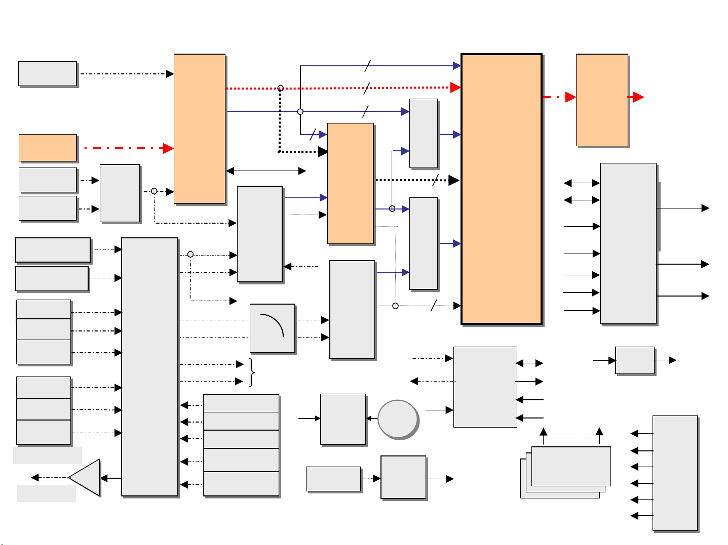
ATSC Input(Sub)
23
HDMI
HDMI
ATSC
ATSC
YPbPr 1
YPbPr 1
YPbPr 2
YPbPr 2
NTSC_CVBS
NTSC_CVBS
ATSC_CVBS
ATSC_CVBS
CVBS 1
CVBS 1
CVBS 2
CVBS 2
CVBS 3
CVBS 3
Y/C 1
Y/C 1
Y/C 2
Y/C 2
Y/C 3
Y/C 3
CVBS & Audio
LINE_OUT
BA7657
7657
7657
CXA2069
(A_S/W)
MST3388
-110
~ 480P
CVBS1
Y1/C1
MICOM_CVBS
CVBS2/Y2
C2
Audio L-Main
Audio R-Main
L/R CVBS1
L/R CVBS2
L/R CVBS3
RGB
HDMI I2S & S/PDIF
uPD
64012
(Video
Decode,
C/C & 3D)
To MSP
L/R SC2
L/R SC2
L/R CVBS1
L/R CVBS2
L/R CVBS3
L/R DVI
L/R DVI
LPF
RGB/FB
For CC
5Vst
MDIN
(I/P)
VPC3230
(Decoder)
Real
Real
Timer
Timer
(M41T81)
(M41T81)
RS232C
RS232C
150
24
4
5
8 Bit
MUX
24
8 Bit
MUX
16
D-H/V Sync & clk
A-INE[23:0]
MDIN
MDIN
150
150
4
A-H/V Sync & clk
D-INO[23:0]
ASI510
(Scaler)
V-H/V Sync & clk
V-IN [15:0]
30
HDMI I2S
ATSC I2S
SIF _A
L/R Main
(CXA2069)
L/R ATSC
L/R DTV1
L/R DTV2
(~DE)
J-
J-
LVDS Tx
L003
L003
DS90C387
(~SOG)
MSP44X0
Audio
Audio
(2069,
(2069,
MSP44X0,
MSP44X0,
4052)
Audio
4052)
Panel
L/R SC2
(CXA2069)
L/R Aux.
(Headphone)
L/R Main
(Power Amp)
From
IIC
MICOM_CVBS
RGB/FB
Bat.
Bat.
232C
MAX232
MAX232
Rx/Tx
Rx/Tx
SDA6000M
Tele-text
C/C
IIC
LED
Key
I/R
MSP4440
Output
I/O
Expender
MAX232
MAX232
Amp
Amp
Speaker
. M7V
. A6VCC
. A12VCC
. 12VCC
. 2V5VCC
. 3V3VCC
Page 24
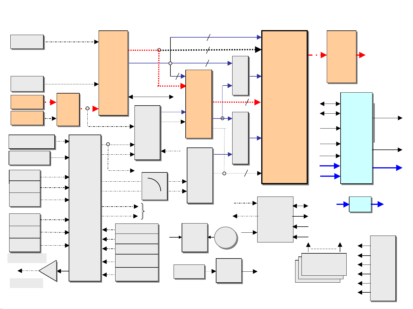
Component Input(Main)
24
HDMI
HDMI
ATSC
ATSC
YPbPr 1
YPbPr 1
YPbPr 2
YPbPr 2
NTSC_CVBS
NTSC_CVBS
ATSC_CVBS
ATSC_CVBS
CVBS 1
CVBS 1
CVBS 2
CVBS 2
CVBS 3
CVBS 3
Y/C 1
Y/C 1
Y/C 2
Y/C 2
Y/C 3
Y/C 3
CVBS & Audio
LINE_OUT
BA7657
7657
7657
CXA2069
(A_S/W)
MST3388
-110
~ 480P
CVBS1
Y1/C1
MICOM_CVBS
CVBS2/Y2
C2
Audio L-Main
Audio R-Main
L/R CVBS1
L/R CVBS2
L/R CVBS3
RGB
HDMI I2S & S/PDIF
uPD
64012
(Video
Decode,
C/C & 3D)
To MSP
L/R SC2
L/R SC2
L/R CVBS1
L/R CVBS2
L/R CVBS3
L/R DVI
L/R DVI
LPF
RGB/FB
For CC
5Vst
MDIN
(I/P)
VPC3230
(Decoder)
Real
Real
Timer
Timer
(M41T81)
(M41T81)
RS232C
RS232C
150
24
4
5
8 Bit
MUX
24
8 Bit
MUX
16
D-H/V Sync & clk
A-INE[23:0]
A-H/V Sync & clk
4
MDIN
MDIN
150
D-INO[23:0]
150
ASI510
(Scaler)
V-H/V Sync & clk
V-IN [15:0]
(~DE)
30
(~SOG)
SIF _A
L/R Main
(CXA2069)
L/R ATSC
L/R DTV1
L/R DTV2
LVDS Tx
DS90C387
HDMI I2S
ATSC I2S
J-
J-
L003
L003
Audio
Audio
(2069,
(2069,
MSP44X0,
MSP44X0,
4052)
Audio
4052)
MSP44X0
Panel
L/R SC2
(CXA2069)
L/R Aux.
(Headphone)
L/R Main
(Power Amp)
From
IIC
MICOM_CVBS
RGB/FB
Bat.
Bat.
232C
MAX232
MAX232
Rx/Tx
Rx/Tx
SDA6000M
Tele-text
C/C
IIC
LED
Key
I/R
MSP4440
Output
I/O
Expender
MAX232
MAX232
Amp
Amp
Speaker
. M7V
. A6VCC
. A12VCC
. 12VCC
. 2V5VCC
. 3V3VCC
Page 25
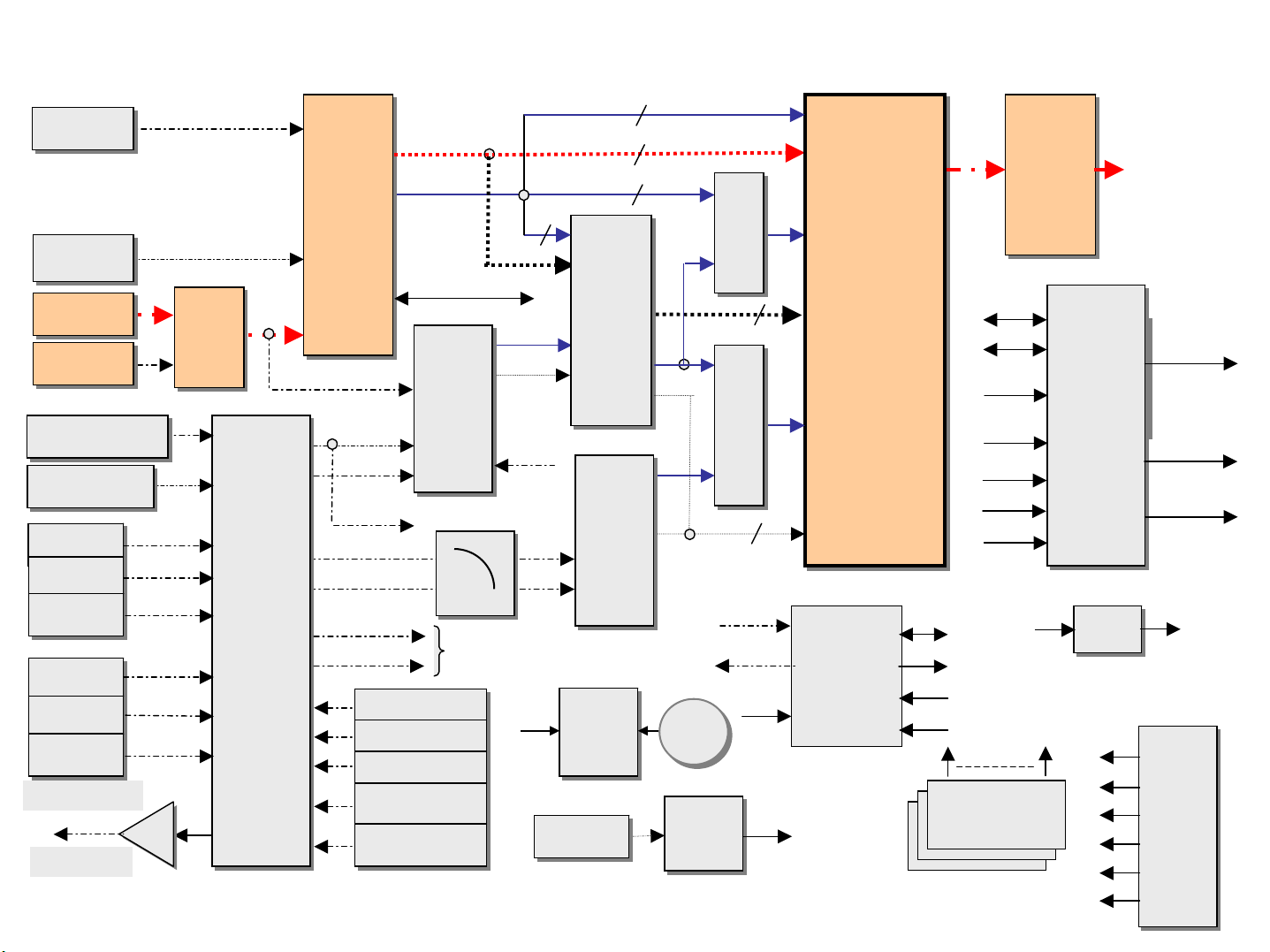
Component Input(Sub)
25
HDMI
HDMI
ATSC
ATSC
YPbPr 1
YPbPr 1
YPbPr 2
YPbPr 2
NTSC_CVBS
NTSC_CVBS
ATSC_CVBS
ATSC_CVBS
CVBS 1
CVBS 1
CVBS 2
CVBS 2
CVBS 3
CVBS 3
Y/C 1
Y/C 1
Y/C 2
Y/C 2
Y/C 3
Y/C 3
CVBS & Audio
LINE_OUT
BA7657
7657
7657
CXA2069
(A_S/W)
MST3388
-110
~ 480P
CVBS1
Y1/C1
MICOM_CVBS
CVBS2/Y2
C2
Audio L-Main
Audio R-Main
L/R CVBS1
L/R CVBS2
L/R CVBS3
RGB
HDMI I2S & S/PDIF
uPD
64012
(Video
Decode,
C/C & 3D)
To MSP
L/R SC2
L/R SC2
L/R CVBS1
L/R CVBS2
L/R CVBS3
L/R DVI
L/R DVI
LPF
RGB/FB
For CC
5Vst
MDIN
(I/P)
VPC3230
(Decoder)
Real
Real
Timer
Timer
(M41T81)
(M41T81)
RS232C
RS232C
150
24
4
5
8 Bit
MUX
24
8 Bit
MUX
16
D-H/V Sync & clk
A-INE[23:0]
4
A-H/V Sync & clk
MDIN
MDIN
150
D-INO[23:0]
150
ASI510
(Scaler)
V-H/V Sync & clk
V-IN [15:0]
(~DE)
30
(~SOG)
SIF _A
L/R Main
(CXA2069)
L/R ATSC
L/R DTV1
L/R DTV2
LVDS Tx
DS90C387
HDMI I2S
ATSC I2S
J-
J-
L003
L003
Audio
Audio
(2069,
(2069,
MSP44X0,
MSP44X0,
4052)
Audio
4052)
MSP44X0
Panel
L/R SC2
(CXA2069)
L/R Aux.
(Headphone)
L/R Main
(Power Amp)
From
IIC
MICOM_CVBS
RGB/FB
Bat.
Bat.
232C
MAX232
MAX232
Rx/Tx
Rx/Tx
SDA6000M
Tele-text
C/C
IIC
LED
Key
I/R
MSP4440
Output
I/O
Expender
MAX232
MAX232
Amp
Amp
Speaker
. M7V
. A6VCC
. A12VCC
. 12VCC
. 2V5VCC
. 3V3VCC
Page 26
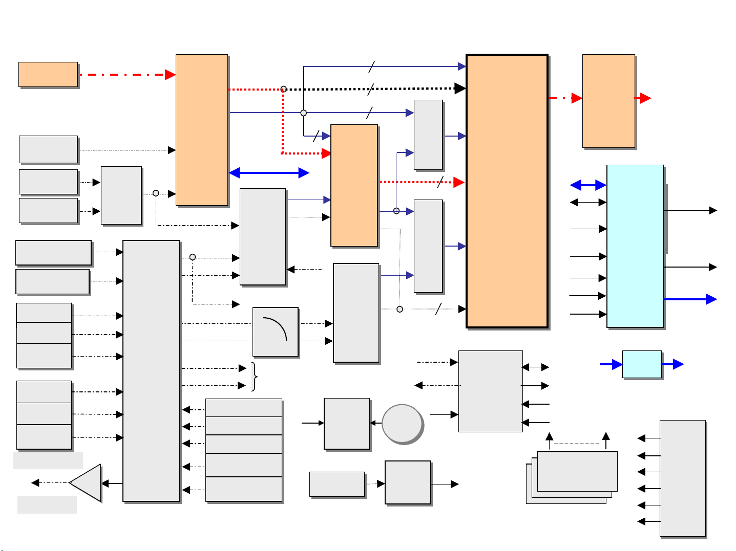
HDMI Input(Main)
26
HDMI
HDMI
ATSC
ATSC
YPbPr 1
YPbPr 1
YPbPr 2
YPbPr 2
NTSC_CVBS
NTSC_CVBS
ATSC_CVBS
ATSC_CVBS
CVBS 1
CVBS 1
CVBS 2
CVBS 2
CVBS 3
CVBS 3
Y/C 1
Y/C 1
Y/C 2
Y/C 2
Y/C 3
Y/C 3
CVBS & Audio
LINE_OUT
BA7657
7657
7657
CXA2069
(A_S/W)
MST3388
-110
~ 480P
CVBS1
Y1/C1
MICOM_CVBS
CVBS2/Y2
C2
Audio L-Main
Audio R-Main
L/R CVBS1
L/R CVBS2
L/R CVBS3
RGB
HDMI I2S & S/PDIF
uPD
64012
(Video
Decode,
C/C & 3D)
To MSP
L/R SC2
L/R SC2
L/R CVBS1
L/R CVBS2
L/R CVBS3
L/R DVI
L/R DVI
LPF
RGB/FB
For CC
5Vst
MDIN
(I/P)
VPC3230
(Decoder)
Real
Real
Timer
Timer
(M41T81)
(M41T81)
RS232C
RS232C
150
24
4
5
8 Bit
MUX
24
8 Bit
MUX
16
D-H/V Sync & clk
A-INE[23:0]
MDIN
MDIN
150
150
4
A-H/V Sync & clk
D-INO[23:0]
ASI510
(Scaler)
V-H/V Sync & clk
V-IN [15:0]
30
HDMI I2S
ATSC I2S
SIF _A
L/R Main
(CXA2069)
L/R ATSC
L/R DTV1
L/R DTV2
(~DE)
J-
J-
LVDS Tx
L003
L003
DS90C387
(~SOG)
MSP44X0
Audio
Audio
(2069,
(2069,
MSP44X0,
MSP44X0,
4052)
Audio
4052)
Panel
L/R SC2
(CXA2069)
L/R Aux.
(Headphone)
L/R Main
(Power Amp)
From
IIC
MICOM_CVBS
RGB/FB
Bat.
Bat.
232C
MAX232
MAX232
Rx/Tx
Rx/Tx
SDA6000M
Tele-text
C/C
IIC
LED
Key
I/R
MSP4440
Output
I/O
Expender
MAX232
MAX232
Amp
Amp
Speaker
. M7V
. A6VCC
. A12VCC
. 12VCC
. 2V5VCC
. 3V3VCC
Page 27
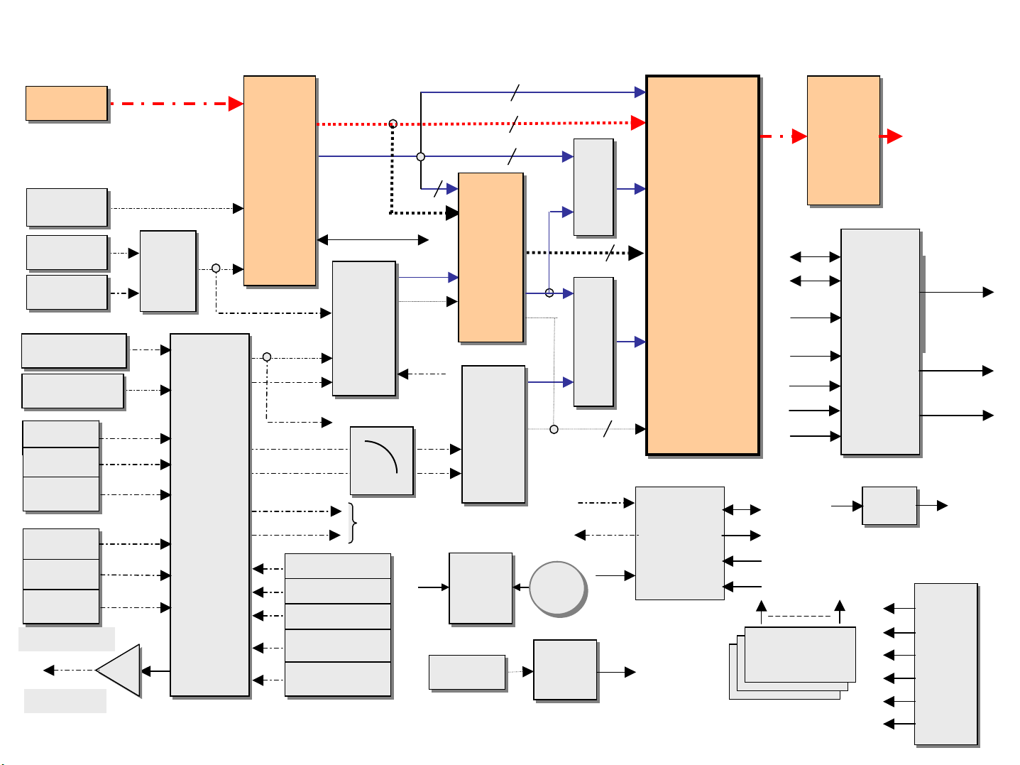
HDMI Input(Sub)
27
HDMI
HDMI
ATSC
ATSC
YPbPr 1
YPbPr 1
YPbPr 2
YPbPr 2
NTSC_CVBS
NTSC_CVBS
ATSC_CVBS
ATSC_CVBS
CVBS 1
CVBS 1
CVBS 2
CVBS 2
CVBS 3
CVBS 3
Y/C 1
Y/C 1
Y/C 2
Y/C 2
Y/C 3
Y/C 3
CVBS & Audio
LINE_OUT
BA7657
7657
7657
CXA2069
(A_S/W)
MST3388
-110
~ 480P
CVBS1
Y1/C1
MICOM_CVBS
CVBS2/Y2
C2
Audio L-Main
Audio R-Main
L/R CVBS1
L/R CVBS2
L/R CVBS3
RGB
HDMI I2S & S/PDIF
uPD
64012
(Video
Decode,
C/C & 3D)
To MSP
L/R SC2
L/R SC2
L/R CVBS1
L/R CVBS2
L/R CVBS3
L/R DVI
L/R DVI
LPF
RGB/FB
For CC
5Vst
MDIN
(I/P)
VPC3230
(Decoder)
Real
Real
Timer
Timer
(M41T81)
(M41T81)
RS232C
RS232C
150
24
4
5
8 Bit
MUX
24
8 Bit
MUX
16
MICOM_CVBS
RGB/FB
IIC
Bat.
Bat.
232C
MAX232
MAX232
Rx/Tx
Rx/Tx
D-H/V Sync & clk
A-INE[23:0]
A-H/V Sync & clk
MDIN
MDIN
150
D-INO[23:0]
150
ASI510
(Scaler)
V-H/V Sync & clk
V-IN [15:0]
SDA6000M
Tele-text
C/C
4
LED
IIC
Key
I/R
30
DS90C387
(~SOG)
HDMI I2S
ATSC I2S
SIF _A
L/R Main
(CXA2069)
L/R ATSC
L/R DTV1
L/R DTV2
From
MSP4440
Output
I/O
Expender
(~DE)
J-
J-
LVDS Tx
L003
L003
Audio
Audio
(2069,
(2069,
MSP44X0,
MSP44X0,
4052)
Audio
4052)
MSP44X0
MAX232
MAX232
Amp
Amp
Panel
L/R SC2
(CXA2069)
L/R Aux.
(Headphone)
L/R Main
(Power Amp)
Speaker
. M7V
. A6VCC
. A12VCC
. 12VCC
. 2V5VCC
. 3V3VCC
Page 28
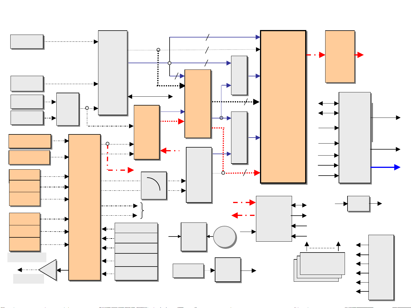
Caption Input
28
HDMI
HDMI
ATSC
ATSC
YPbPr 1
YPbPr 1
YPbPr 2
YPbPr 2
NTSC_CVBS
NTSC_CVBS
ATSC_CVBS
ATSC_CVBS
CVBS 1
CVBS 1
CVBS 2
CVBS 2
CVBS 3
CVBS 3
Y/C 1
Y/C 1
Y/C 2
Y/C 2
Y/C 3
Y/C 3
CVBS & Audio
LINE_OUT
BA7657
7657
7657
CXA2069
(A_S/W)
MST3388
-110
~ 480P
CVBS1
Y1/C1
MICOM_CVBS
CVBS2/Y2
C2
Audio L-Main
Audio R-Main
RGB
HDMI I2S & S/PDIF
uPD
64012
(Video
Decode,
C/C & 3D)
To MSP
L/R SC2
L/R SC2
L/R CVBS1
L/R CVBS1
L/R CVBS2
L/R CVBS2
L/R CVBS3
L/R CVBS3
L/R DVI
L/R DVI
LPF
RGB/FB
For CC
5Vst
MDIN
(I/P)
VPC3230
(Decoder)
Real
Real
Timer
Timer
(M41T81)
(M41T81)
RS232C
RS232C
150
24
4
5
8 Bit
MUX
24
8 Bit
MUX
16
D-H/V Sync & clk
A-INE[23:0]
MDIN
MDIN
150
150
4
A-H/V Sync & clk
D-INO[23:0]
ASI510
(Scaler)
V-H/V Sync & clk
V-IN [15:0]
30
(~SOG)
HDMI I2S
ATSC I2S
SIF _A
L/R Main
(CXA2069)
L/R ATSC
L/R DTV1
L/R DTV2
(~DE)
LVDS Tx
L003
L003
DS90C387
J-
J-
Audio
Audio
(2069,
(2069,
MSP44X0,
MSP44X0,
4052)
Audio
4052)
MSP44X0
Panel
L/R SC2
(CXA2069)
L/R Aux.
(Headphone)
L/R Main
(Power Amp)
From
IIC
MICOM_CVBS
RGB/FB
Bat.
Bat.
232C
MAX232
MAX232
Rx/Tx
Rx/Tx
SDA6000M
Tele-text
C/C
IIC
LED
Key
I/R
MSP4440
Output
I/O
Expender
MAX232
MAX232
Amp
Amp
Speaker
. M7V
. A6VCC
. A12VCC
. 12VCC
. 2V5VCC
. 3V3VCC
Page 29
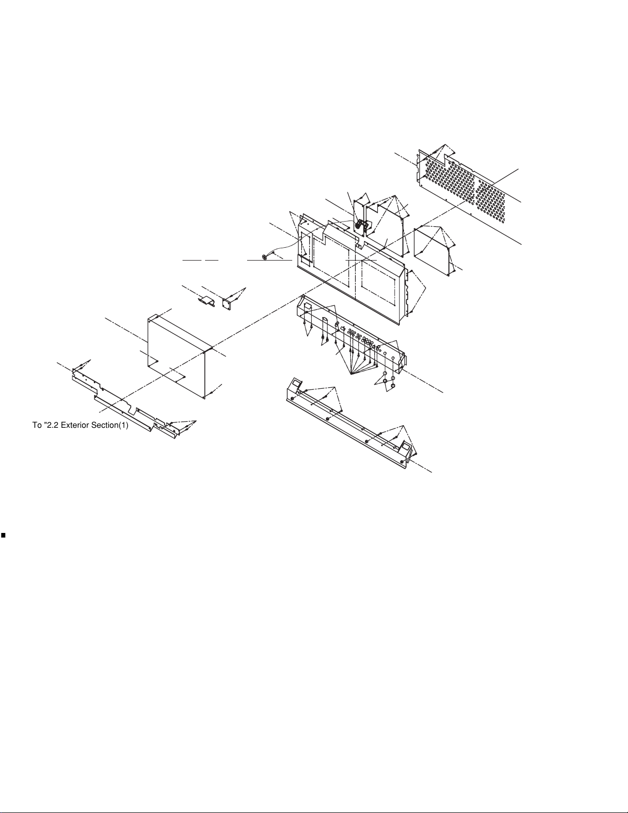
Tuner / Digital / Input & SMPS Power Modules
29
21
11
10
12
10
3
10
10
4
10
9
10
10
To "2.5 Rear Section
1
22
To "2.2 Exterior Section(1)
10
10
12
7
6
10
10
10
1 SMPS Assy 150-2040
2 DTT_ANALOG Assy 010-2640
3 DIGITAL Assy 010-2741
4 EMI FILTER PCB Assy 010-2742
5• • • •
6 BRKT FAN-TOP 30172-01-001
7FAN D05X12TL(50x50x10) 10511-07-001
8 Screw M3x14, SEMS,ZNW M1040301415
9 ASSY SHIELD MAIN 01434-0010
10 Screw M3x8, SEMS,ZNW M1040300815
11 BRKT N-FILTER 30173-01-000
12 Screw M3x8, SEM(E),ZNW M1033400615
13 BRKT REAR BOTTOM 30104-03-001
14 Screw T4x16,SS,T/T,BH,BLK M1305401617
15 BRKT MAIN AV-USA 30165-02-001
16 Screw T3x8,2S,T/T,BH,BLK M1305300817
17 Screw M3x8,3S,HH,FNI M1116300805
18 Screw M4x8,BH,BLK M1015400817
19 Wsher (Ø10) M1231111002
20 NUT UNF 3/8INCH832 M1211210002
21 ASSY SHIELD MAIN TOP M1305300817
22 ASSY BRKT MAIN SUPPORTER 01433-0060
8
10
10
Description
16
17
18
10
14
2
16
18
16
19
20
14
ar
P
t No.
15
13
Page 30

ADJUSTMENT
30
1. At shipment, the unit is adjusted to its best conditions. Normally, it is not necessary to readjust even if an assembly is replaced. If the
adjustment is shifted or if it becomes necessary to readjust because of part replacement, etc., perform the adjustment as described below.
2. Any value changed in Service/Factory mode will be stored in memory as soon as it is changed. Before readjustment, take note of the
original values for reference in case you need to restore the original settings.
3. Use a stable AC power supply.
ADJUSTMENT OF WHITE BALANCE
Adjustment of White Balance
1. Equipment
• MIK7255 or Pattern Generator
• CA-210 Display Color Analyzer
• Remote Control.
2. Pattern adjustment
• ADC Calibration : Mik pattern #240
• Auto-Calibration Mode ; 480p/60Hz
; 720p/60Hz
; 480i/60Hz
• White Balance adjustment pattern: Mik pattern #446
• Color coordinate adjustment Mode: 720p/60Hz(Component)
Composite NTSC
3. STEP1: ADC-Calibration
1) At 480p, do Auto-Calibration of ADC-cut off & Gain(1 ) on Mosaic pattern(ex Mik pattern #240)
2) At 720p/60Hz, repeat 1)
3) At 480i, repeat 1).
STEP2: Adjustment of White - Balance
4.
1) At Component input 1. 720p/60Hz, adjust white Balance Mid , High ,Low at pattern Full white 70%
(Ex; Mik pattern #446)
2) At Composite NTSC, repeat 1)
3) White Balance coordination (enter White Balance in Factory Mode)
How to enter; TV/AV -> 0 -> 9 -> 1-> 7 (press buttons one at a time to enter factory mode)
-> ASI510 W/B -> Done (it shows R,G,B adjustment toolbar)
(1) Mid : x=0.283 , y=0.298 +/- 0.02 (9300k)
(2) High : x=0.276 , y=0.283 +/- 0.02 (11000k)
(3) Low : x=0.313 , y=0.329 +/- 0.02 (6500k)
Page 31

Power Down – Quick Troubleshooting Tip
31
Plasma Panel shuts down immediately
After power on.
First unplug the two connectors on the SMPS
Assembly (the connectors with all brown wires).
Next unplug the TMDS connector from the
Display to the panel assembly (silver shielded
connector).
Try to power the set on in this condition. If the
power stays on you will need to troubleshoot the
Panel assembly PCB’s. If the power still shuts
down you need to troubleshoot the Display, DTT,
SMPS Audio or Thermal sensor assemblies.
Page 32
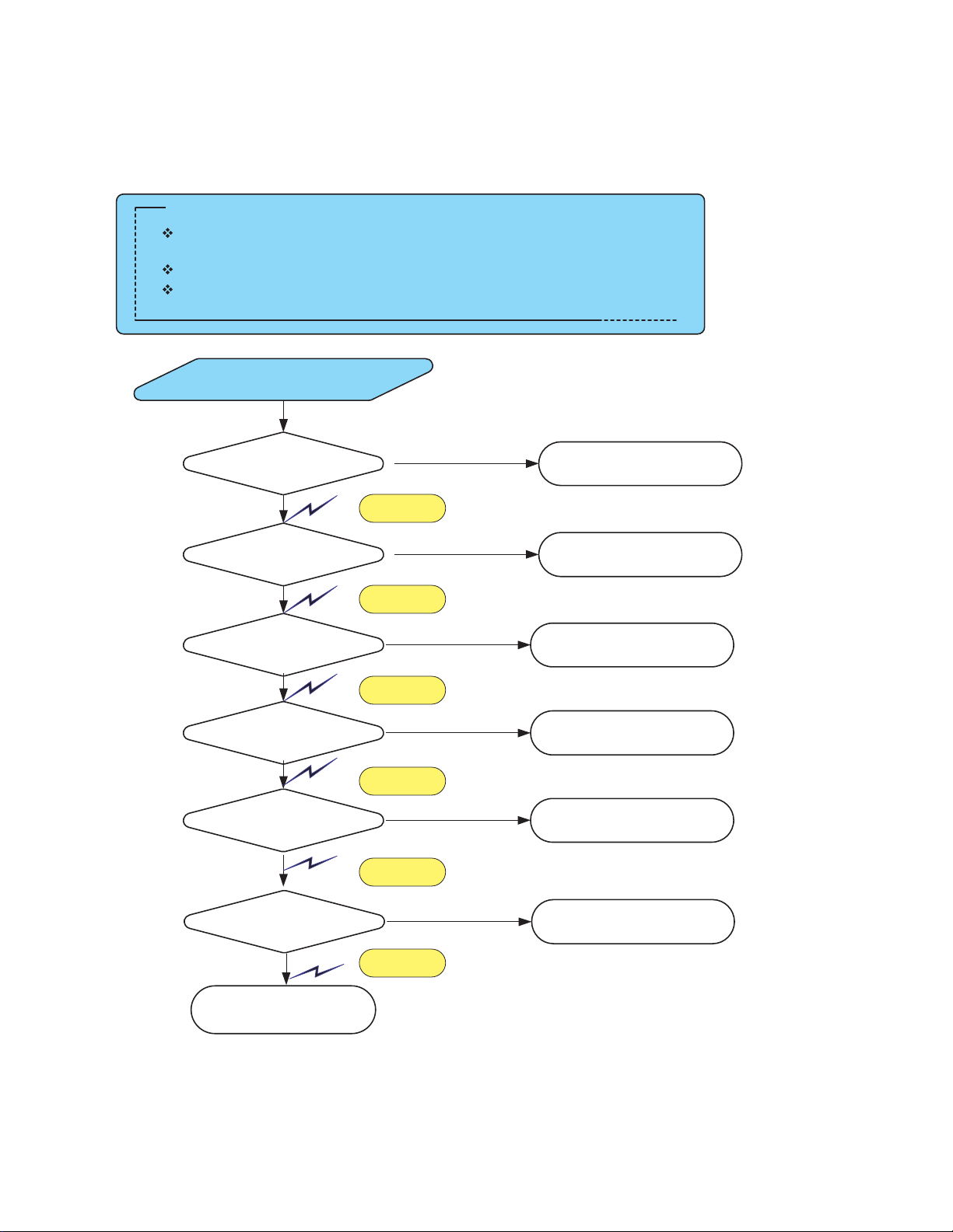
1. No Power
32
(Power Supply Board)
Preliminary Checkpoints
Check the condition of the input power &cable connection.
(JP730,JP701(DTT&Analog, JP709(Digital),JP230(AMP))
Check the condition of on-board regulators.
Check for short circuits between each power terminal and the ground.
No Power
When Powered ON
#1(M-7V)
at JP730
In Digital B/D
#3(Power)
at JP730
In digital Board
#5(POMUTE)
at JP730
In digital Board
#74,75
at U29
in digital B/D
The signal waveform
of X3
in digital B/D
Waveform 1
Waveform 2
Waveform 3
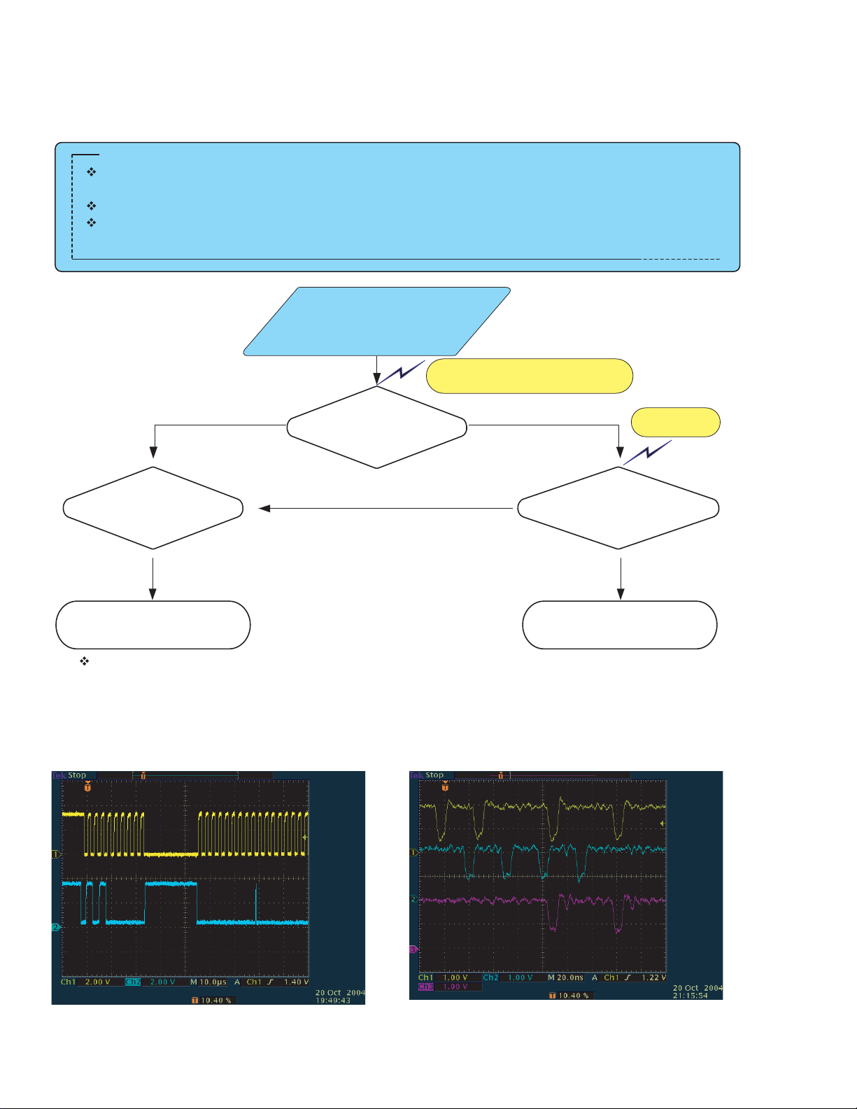
Waveform
4,4 - 1
Waveform 5
NG
NG
NG
NG
NG
Check SMPS
Check SMPS &Micom
Block(U29)
Check SMPS &Power Line
in Digital B/D
Check the state of soldering
in U401,U800,U29
Check the input power
part in U29
The data line waveform
of U28
Change Digital B/D
Waveform
6,6 - 1
NG
Check the U28 and
related Circuit
Page 33
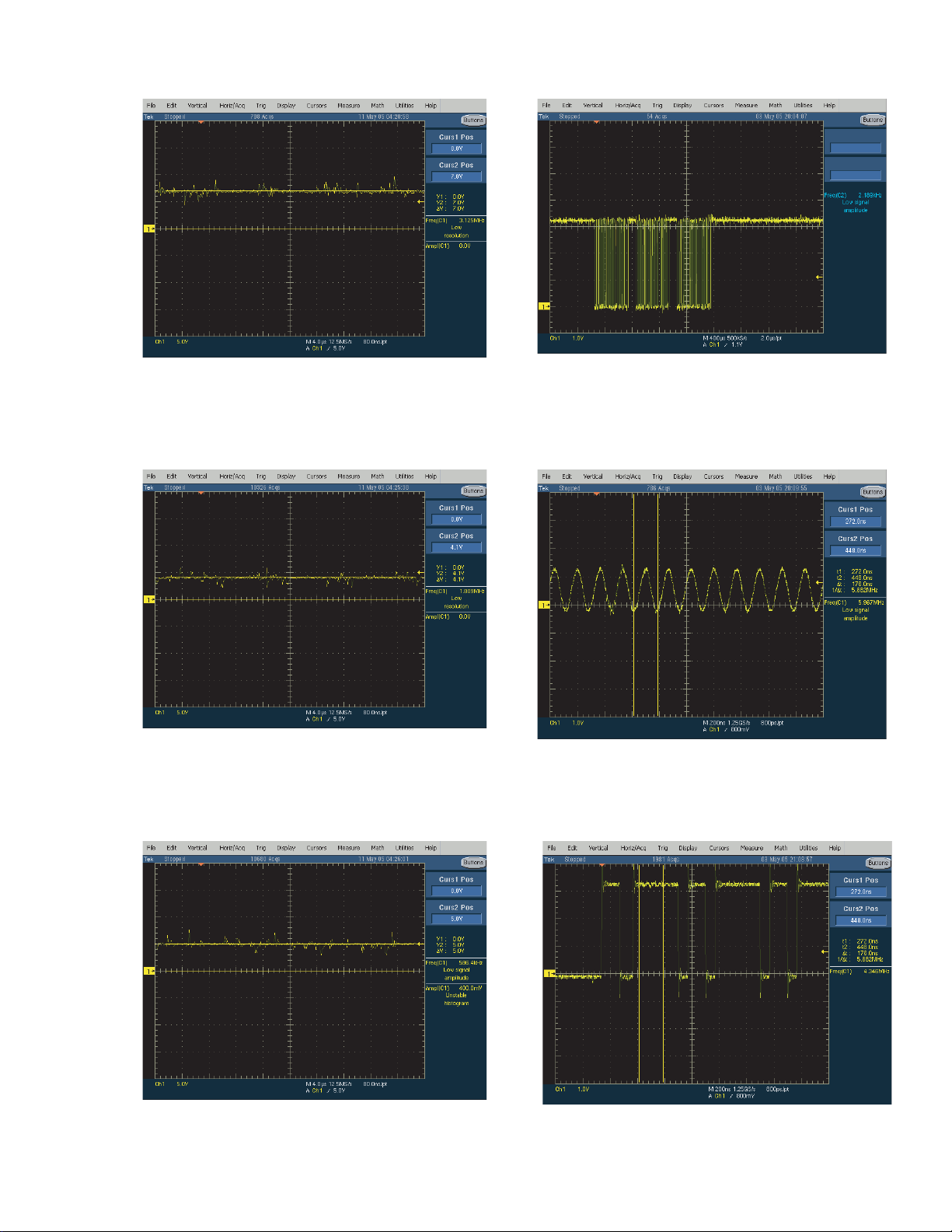
<Waveform 1 >
33
<Waveform 4-1 >
<Waveform 2 >
<Waveform 3 > <Waveform 6-1 >
<Waveform 5 >
Page 34
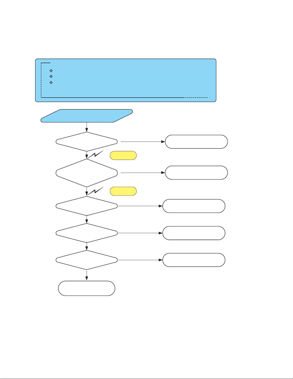
2. No HDMI Signal
34
Preliminary Checkpoints
Check the condition of Conection of the HDMI input Connector
Check the condition of Soldering state in HDMI input part.
Check for short circuits between each power terminal and the ground.
No HDMI
signal
#37,38
at U401
in digital B/D
#108,109,111,112,
114,115,117,118
DC level At U401
In digital Board
EDID data
at U4
In digi tal Board
No sound
in HDMI mode
Check the signal
at JP4(HDMI Connector)
Waveform 7
Waveform 8
NG
NG
NG
NG
NG
Check the state of soldering
at U401,U800,U29
Check input signal part of
U401
Check HDMI_PWR
&5VSTB
Check the EDID data
&Audio output at U401
Change JP4
Change Digital B/D
Page 35
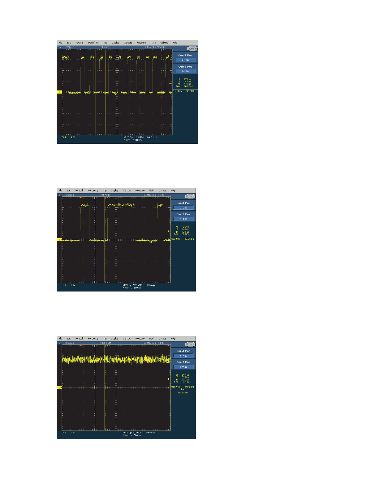
<Waveform 7 SCL >
35
<Waveform 7 SDA >
<Waveform 8 >
Page 36
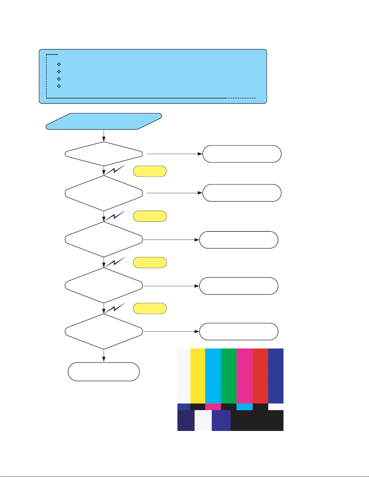
3. No Component Video Signal
36
Preliminary Checkpoints
Check the condition of connectin of the input component video signal.
Check the condition of soldering state in U401
Check the short point in signal l ine.
Check for short circuits between each power terminal and the ground.
No Component
signal (SMPTE Color Bars)
#22,25,27
at U1
in digital B/D
The output signal
At U401
In digital Board
Dose the signal
appear at PR14~19
In digital B/D
Dose the signal
appear at
PR29,31,34,35,38,39
In digital B/D
Waveform 9
Waveform 10
Waveform 11
Waveform 12
NG
NG
NG
NG
Check the state of soldering
at JP1 &input signal part
Check U401 and
Y400 and related circuit
Check U16 and
Y2 and related circuit
Check U20 and
X2 and related circuit
Check the LVDS Cable
and JP500
in Digital B/D
Change Digital B/D
NG
Change the LVDS Cable
&LVDS chip
Test Patterm : SMPTE Color Bats
Page 37
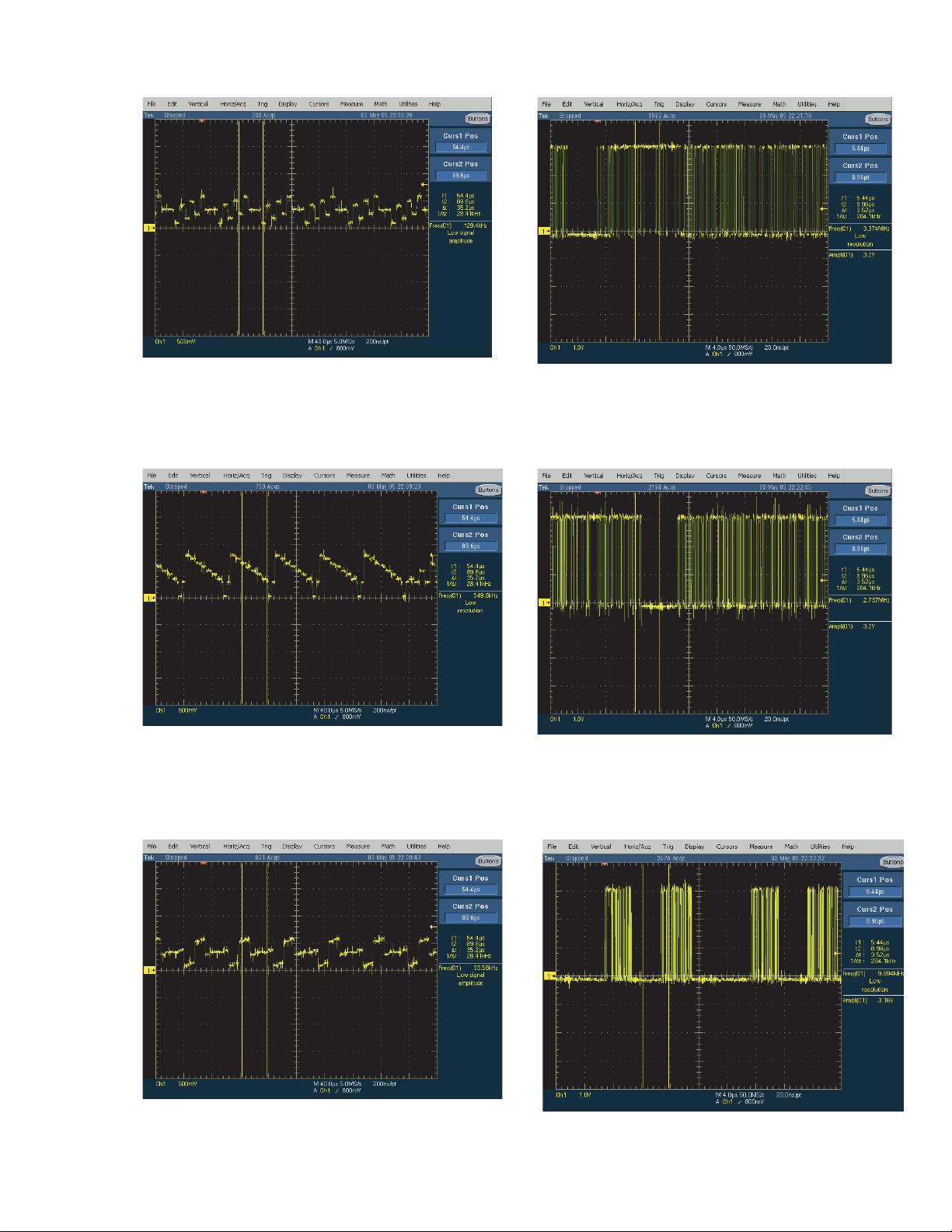
< Waveform 9 #22 >
37
< Waveform 10 >
< Waveform 9 #25 >
< Waveform 9 #27 > < Waveform 12 >
< Waveform 11 >
Page 38
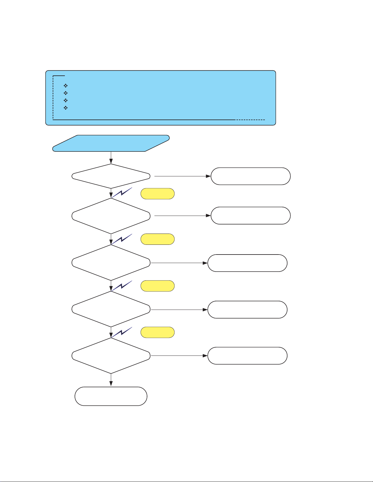
4. No TV Signal
38
Preliminary Checkpoints
Check the condition of connectin of the input TV signal.
Check the condition of soldering state in Tuner & input part
Check the short point in signal line.
Check for short circuits between each power terminal and the ground.
No TV
signal (SMPTE Color Bars)
#63
at U706
in DTT & Analog B/D
#119
At U711
In DTT&Analog Board
Dose the signal
appear at PR22,24
25,26 In DTT&Analog
B/D
Dose the signal
appear at
PR29,31,34,35,38,39
In digital B/D
Waveform 13
Waveform 14
Waveform 11
Waveform 12
NG
NG
NG
NG
Check A_CVBS1 input
part
Check U706 &
input part of U711
Check U16 and
Y2 and related circuit
Check U20 and
X2 and related circuit
Check the LVDS Cable
and JP500
in Digital B/D
Change Digital B/D
NG
Change the LVDS Cable
&LVDS chip
Page 39

< Waveform 13 >
39
< Waveform 14 >
< Waveform 12 >
< Waveform 11 >
Page 40

5. No Video Signal (CVBS)
40
Preliminary Checkpoints
Check the condition of connectin of the input CVBS signal.
Check the condition of soldering state in CVBS & input part
Check the short point in signal line.
Check for short circuits between each power terminal and the ground.
No CVBS
signal (SMPTE Color Bars)
#8(1),15(2),22(3)
at U706
in DTT & Analog B/D
(1):VIDEO01
(2):VIDEO01
(3):VIDEO01
Waveform 15
NG
Check CVBS input
part
#119
At U711
In DTT&Analog Board
Dose the signal
appear at PR22,24
25,26 In DTT&Analog
B/D
Dose the signal
appear at
PR29,31,34,35,38,39
In digital B/D
Check the LVDS Cable
and JP500
in Digital B/D
Waveform 14
Waveform 11
Waveform 12
NG
NG
NG
NG
Check U706 &
input part of U711
Check U16 and
Y2 and related circuit
Check U20 and
X2 and related circuit
Change the LVDS Cable
&LVDS chip
Change Digital B/D
Page 41
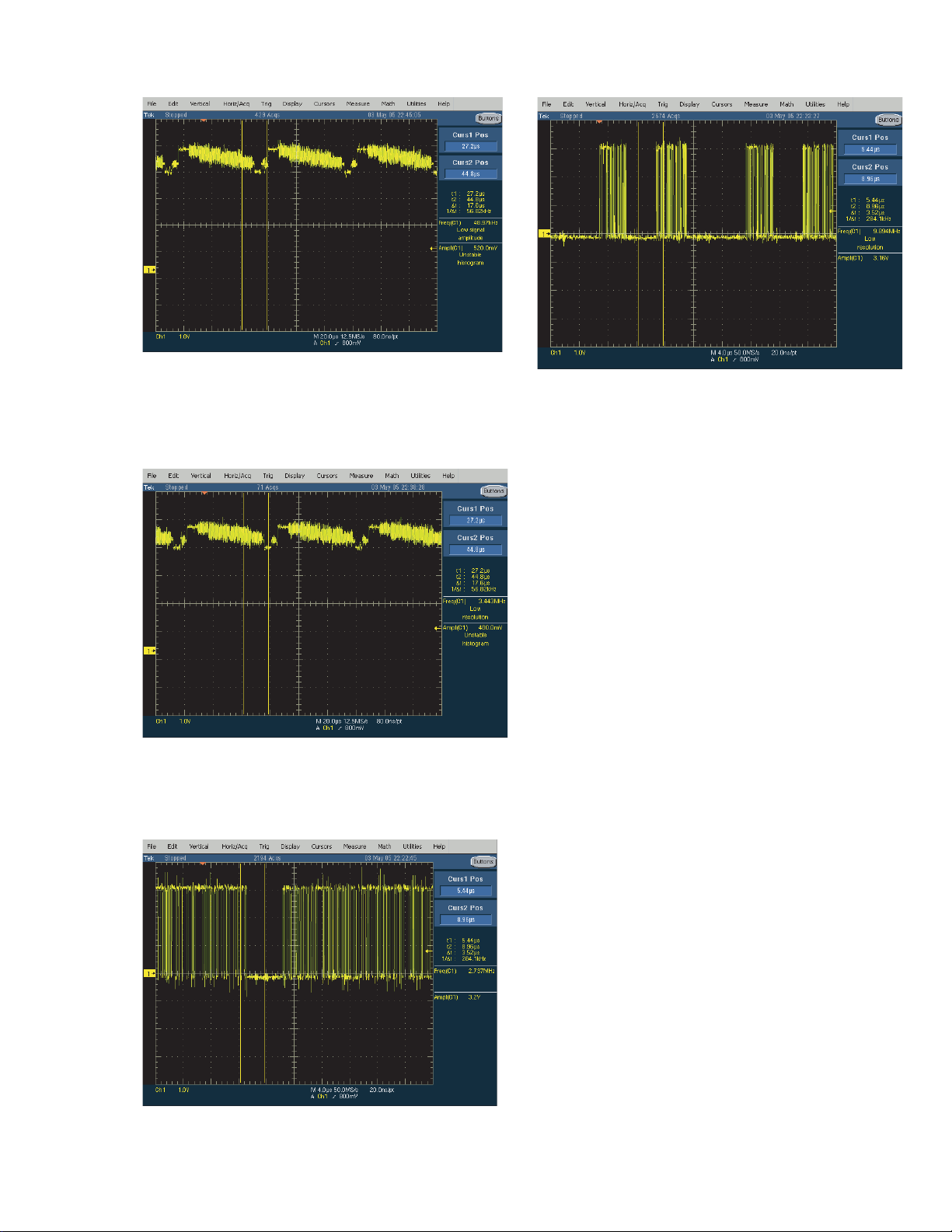
< Waveform 15 >
41
< Waveform 14 >
< Waveform 12 >
< Waveform 11 >
Page 42

6. No Video Signal (S-VHS)
42
Preliminary Checkpoints
Check the condition of connectin of the input S-VHS signal.
Check the condition of soldering state in S-VHS & input part
Check the short poi nt in signal line.
Check for short circuits between each power terminal and the ground.
No S-VHS
signal (SMPTE Color Bars)
#10,12(1),17,19(2),24,26(3)
at U706
in DTT & Analog B/D
(1):S-VIDEO01
(2):S-VIDEO01
(3):S-VIDEO01
Waveform
16,16-1
NG
Check CVBS input
part
#121,128
At U711
In DTT&Analog Board
Dose the signal
appear at PR22,24
25,26 In DTT&Analog
B/D
Dose the signal
appear at
PR29,31,34,35,38,39
In digital B/D
Check the LVDS Cable
and JP500
in Digital B/D
Waveform
17,17-1
Waveform 11
Waveform 12
NG
NG
NG
NG
Check U706 &
input part of U711
Check U16 and
Y2 and related circuit
Check U20 and
X2 and related circuit
Change the LVDS Cable
&LVDS chip
Change Digital B/D
Page 43
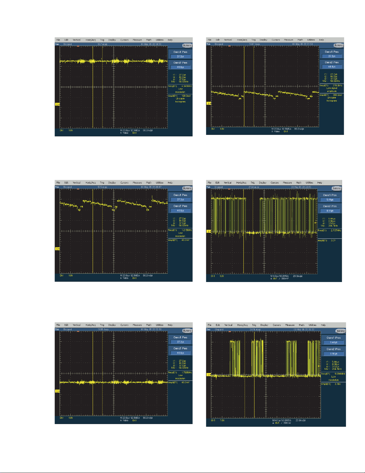
< Waveform 16 C >
43
< Waveform 17 Y >
< Waveform 16 Y >
< Waveform 17 C >
< Waveform 12 >
< Waveform 12 >
Page 44
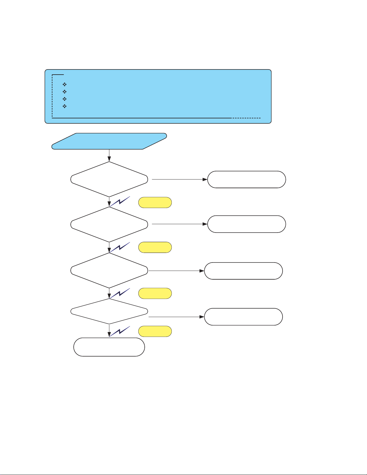
7. No Sound DVI Audio (Sine wave input)
44
Preliminary Checkpoints
Check the condition of connectin of the input DVI Audio R/L.
Check the condition of soldering state in DVI Audio R/L &input part
Check the short point in signal line.
Check for short circuits between each power terminal and the ground.
No Sound in
DVI Audio R/L
#29,31
at U706
in DTT & Analog B/D
#56,57
At U751
In DTT&Analog Board
#11,15
At U200
In Audio Amp Board
#28,31,27,24
At U200
Waveform 18
Waveform 19
Waveform 20
Waveform 21
NG
NG
NG
NG
Check DVI Audio input
part
Check U706 &
input part of U751
Check U751 and
Y800 and related circuit
Check U20 and
X2 and related circuit
Change Speaker
Page 45
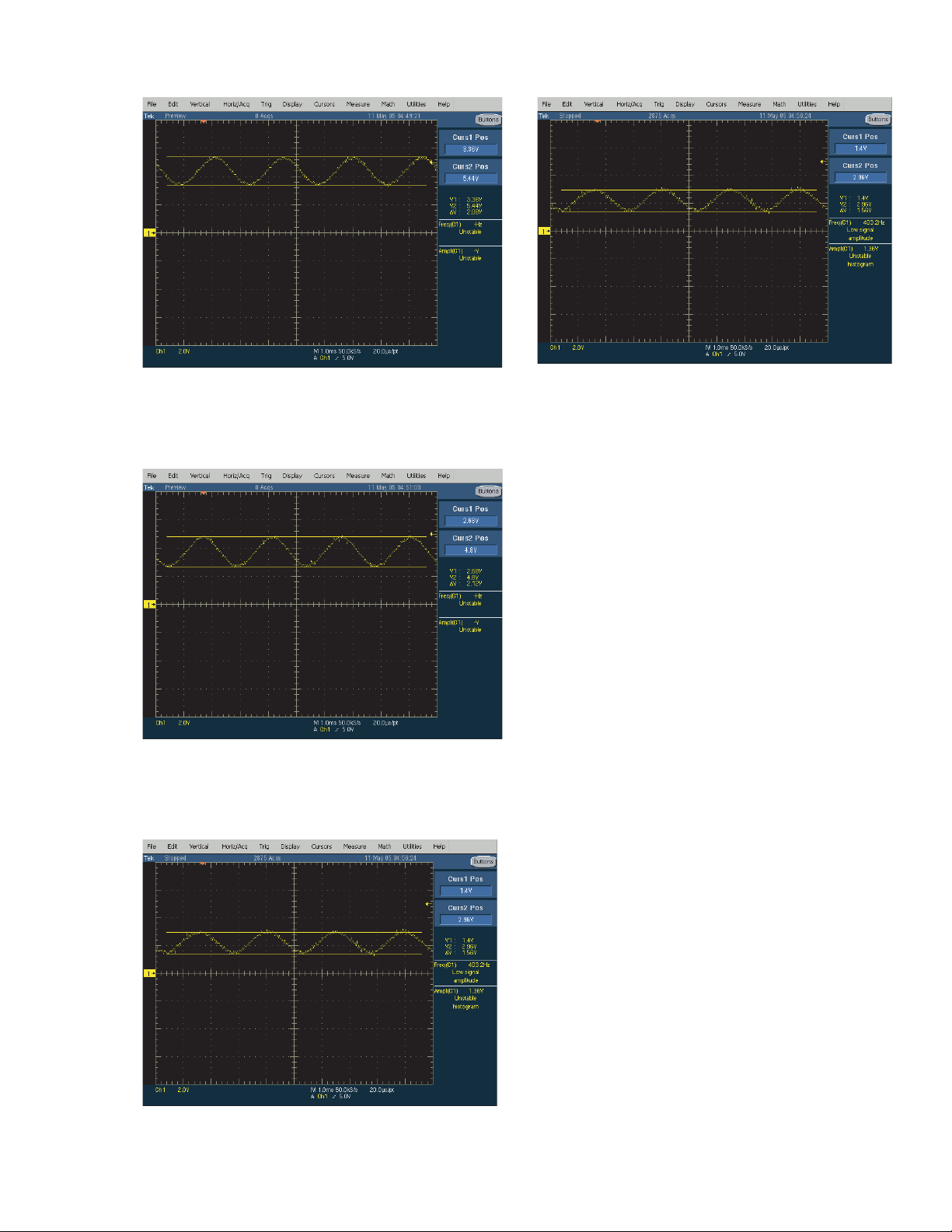
< Waveform 18 >
45
< Waveform 19 >
< Waveform 21 >
< Waveform 20 >
Page 46
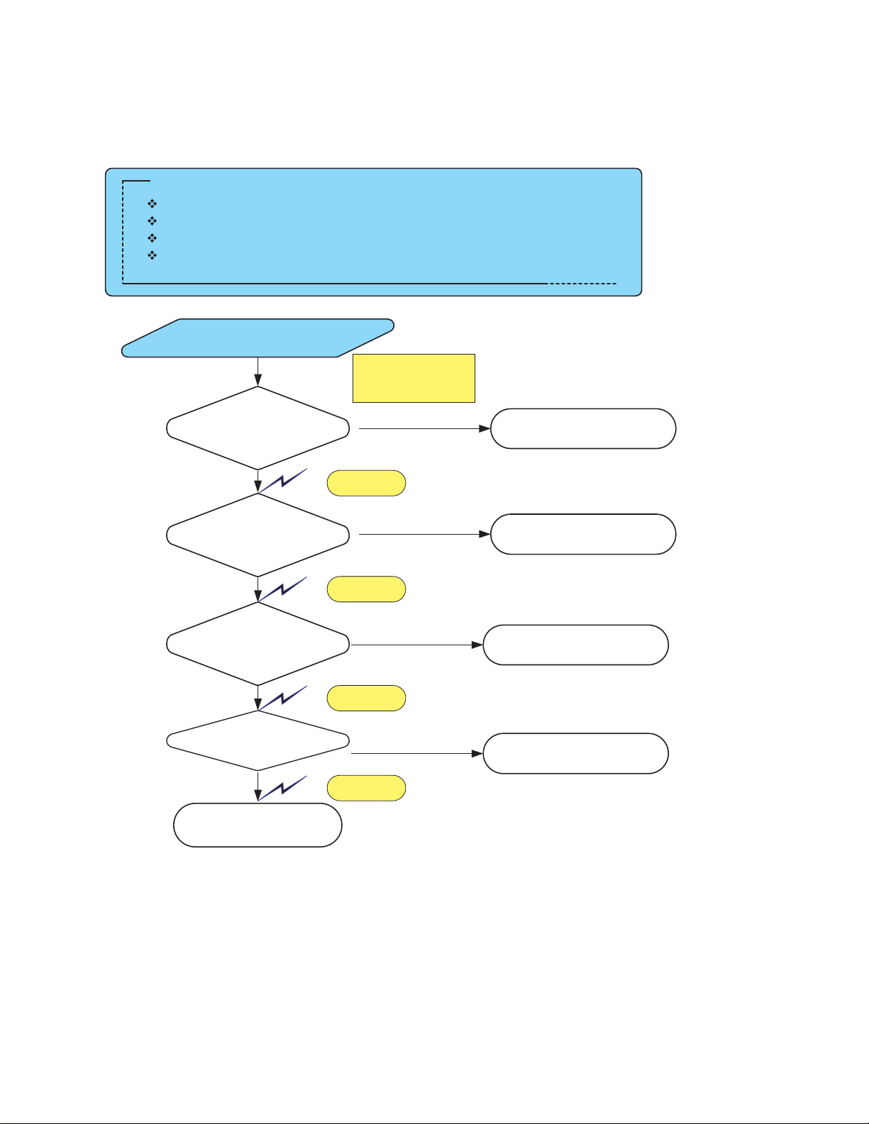
8. No Sound in CVBS (Sine wave input)
46
Preliminary Checkpoints
Check the condition of connectin of the input CVBS Audio R/L.
Check the condition of soldering state in CVBS Audio R/L & input part
Check the short point in signal line.
Check for short circuits between each power terminal and the ground.
No Sound in
CVBS Audio R/L
#9,11(1),16,18(2),23,25(3)
at U706
in DTT & Analog B/D
Waveform 18
(1):VIDEO01 Audio
(2):VIDEO01 Audio
(3):VIDEO01 Audio
NG
Check CVBS Audio input
part
#56,57
At U751
In DTT&Analog Board
#11,15
At U200
In Audio Amp Board
#28,31,27,24
At U200
Change Speaker
Waveform 19
Waveform 20
Waveform 21
NG
NG
NG
Check U706 &
input part of U751
Check U751 and
Y800 and related circuit
Check U200 and
X2 and related circuit
Page 47
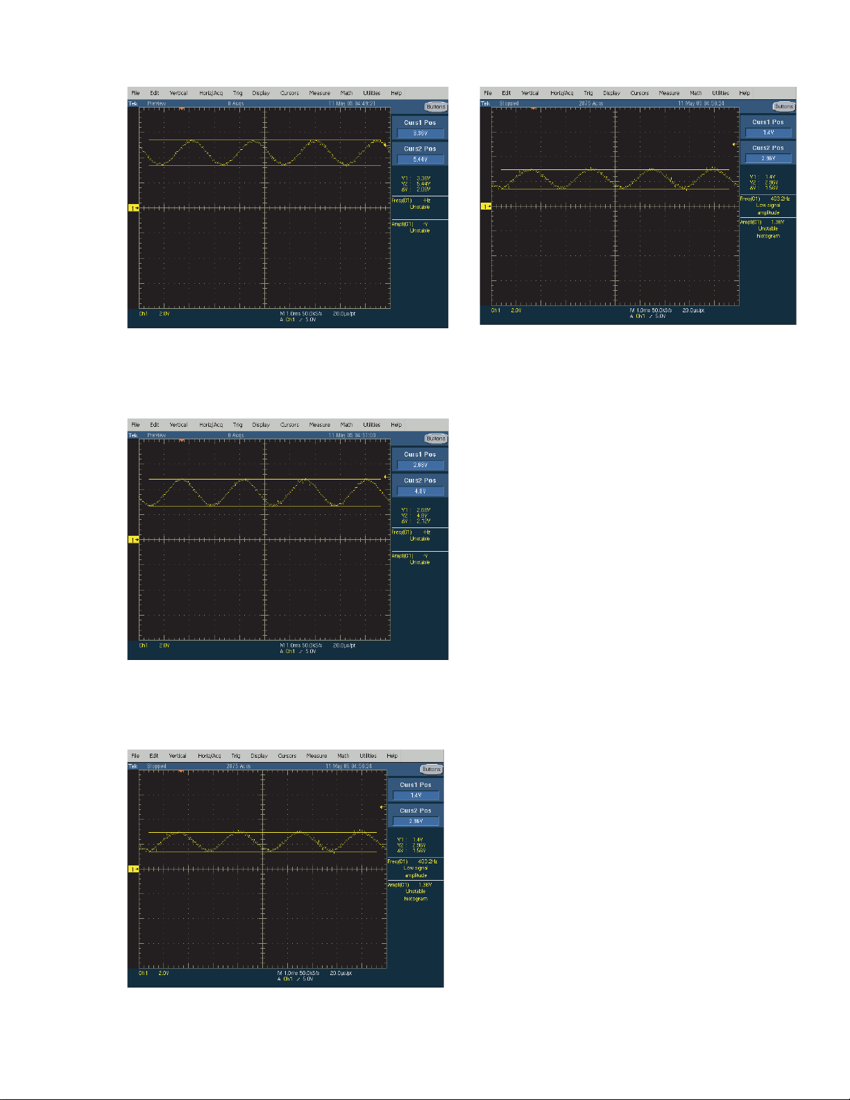
< Waveform 18 >
47
< Waveform 19 >
< Waveform 21 >
< Waveform 20 >
Page 48
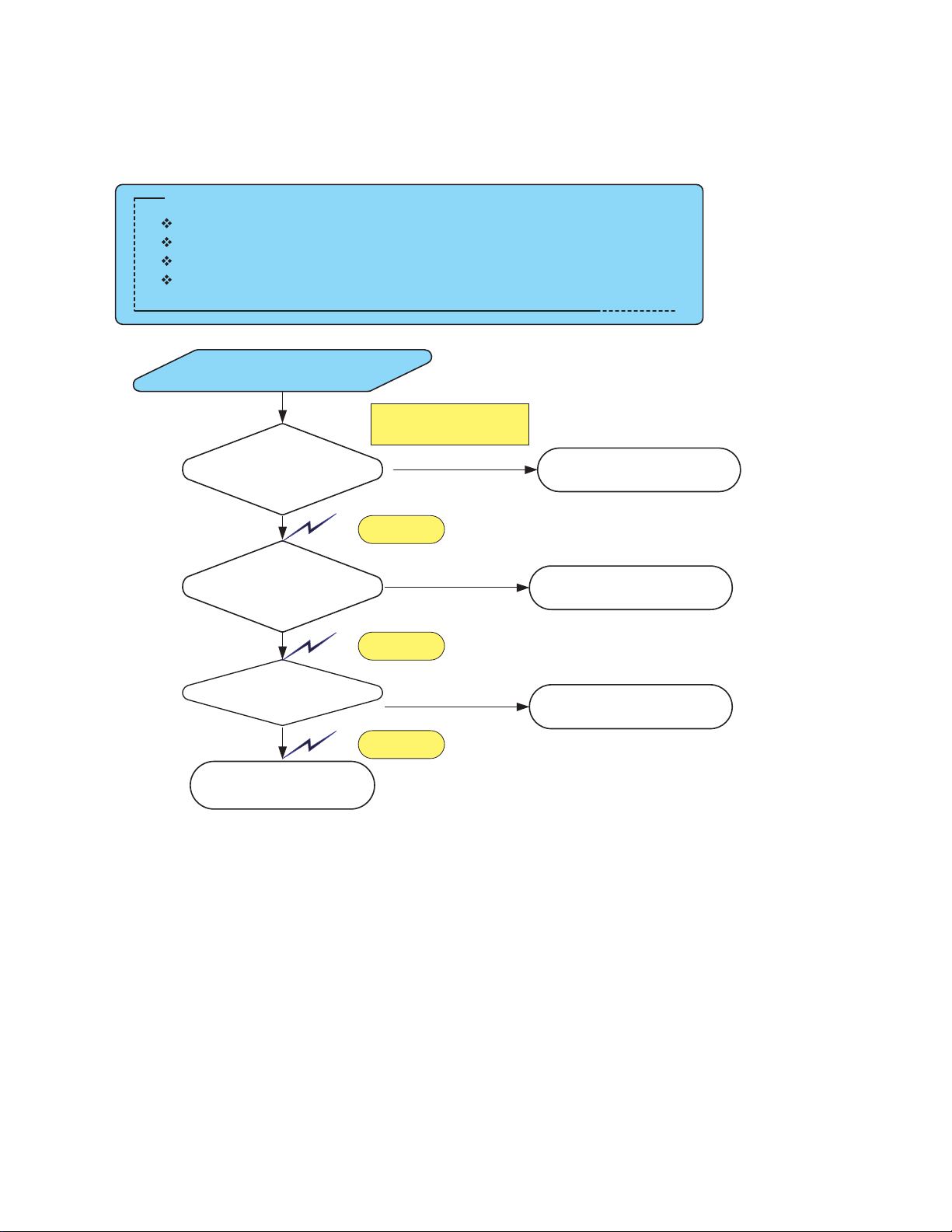
9. No Audio in Component Input (Sine wave input)
48
Preliminary Checkpoints
Check the condition of connectin of the input Component Audio R/L.
Check the condition of soldering state in Component Audio R/L &input part
Check the short point in signal line.
Check for short circuits between each power terminal and the ground.
No Sound in
Component Audio R/L
(1):Component1 Audio
(2):Component2 Audio
#50,51(1),47,48(2)
at U751
in DTT & Analog B/D
Waveform 19
NG
Check Component Audio
input part
#11,15
At U200
In Audio Amp Board
#28,31,27,24
At U200
Change Speaker
Waveform 20
Waveform 21
NG
NG
Check U751 and
Y800 and related circuit
Check U20 and
X2 and related circuit
Page 49
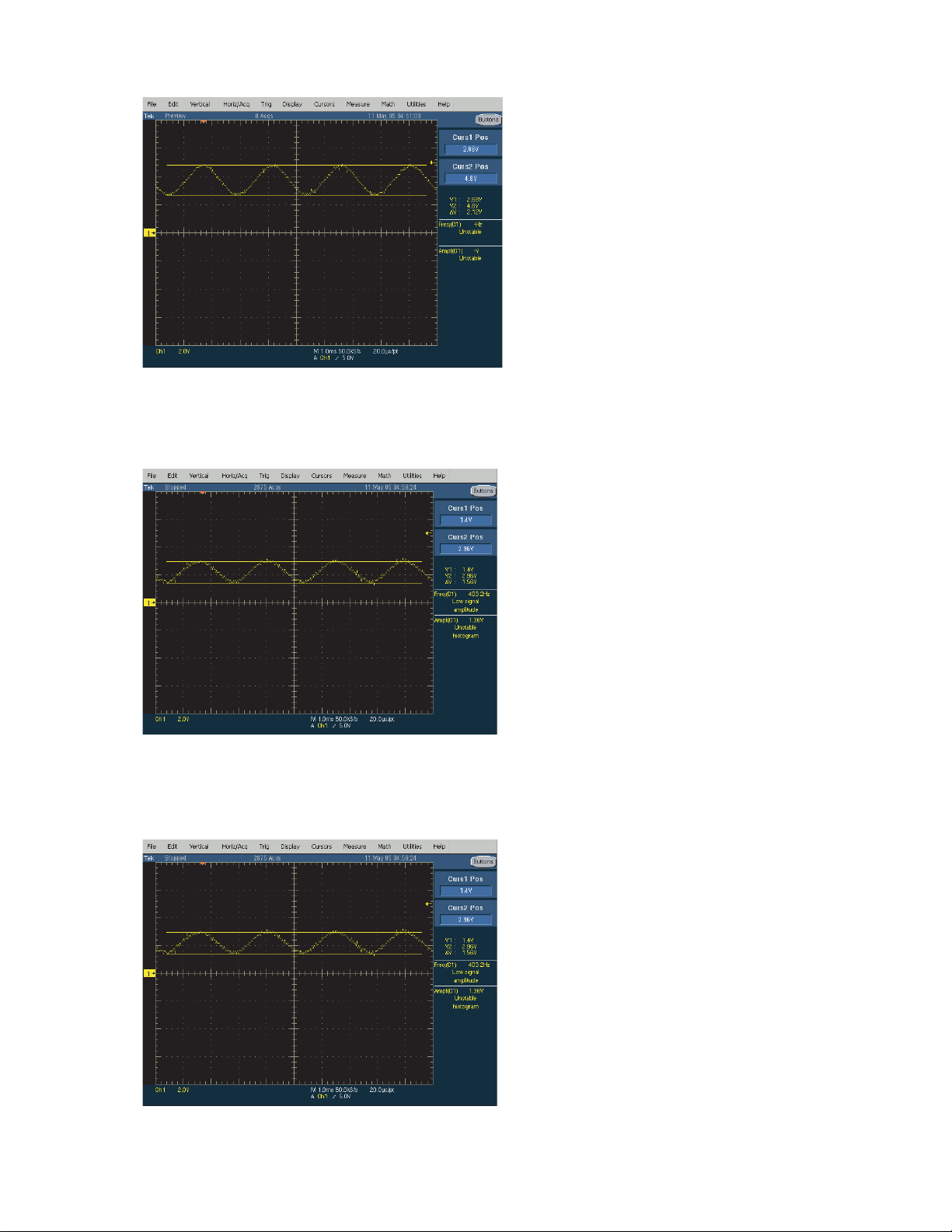
< Waveform 19 >
49
< Waveform 20 >
< Waveform 21 >
Page 50
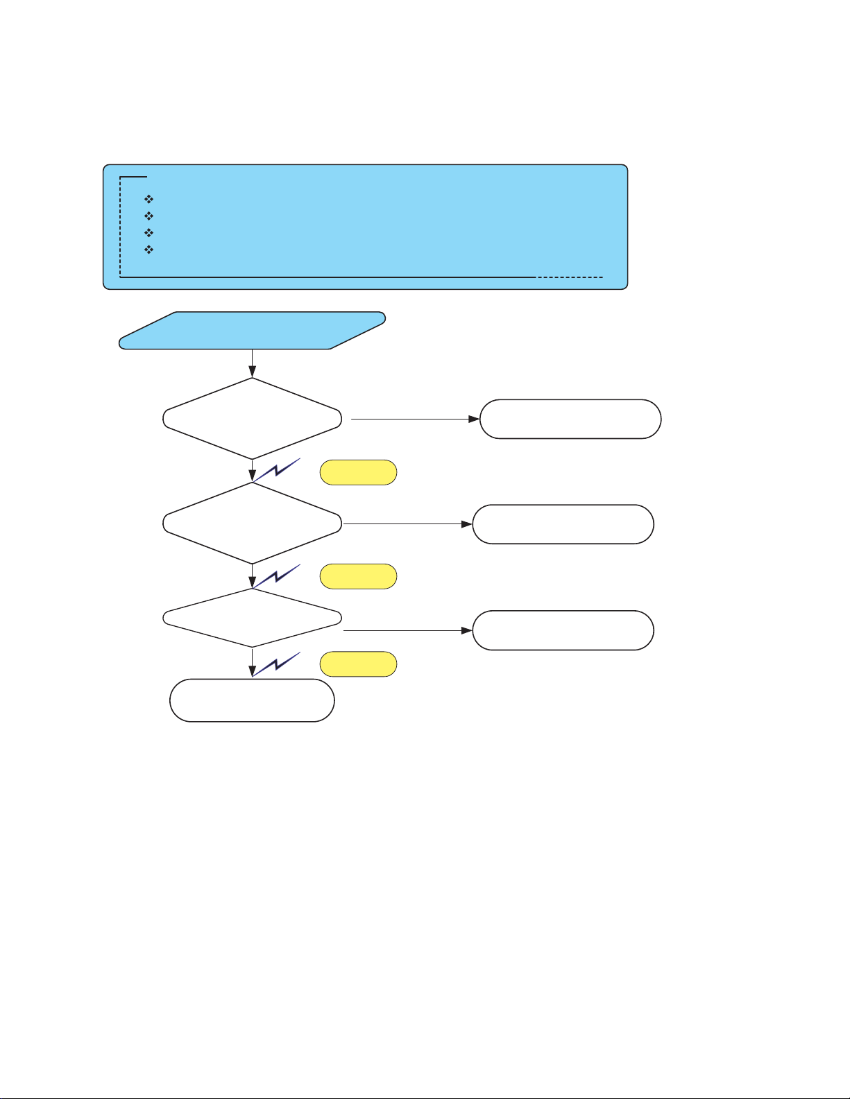
10. No TV Sound (Sine wave input)
50
Preliminary Checkpoints
Check the condition of connectin of the input TV SIF.
Check the condition of soldering state in TV SIF input part.
Check the short point in signal line.
Check for short circuits between each power terminal and the ground.
No Sound in
TV input
#67
at U751
in DTT & Analog B/D
#11,15
At U200
In Audio Amp Board
#28,31,27,24
At U200
Change Speaker
Waveform 22
Waveform 20
Waveform 21
NG
NG
NG
Check TV SIF input part
Check U751 and
Y800 and related circuit
Check U20 and
X2 and related circuit
Page 51
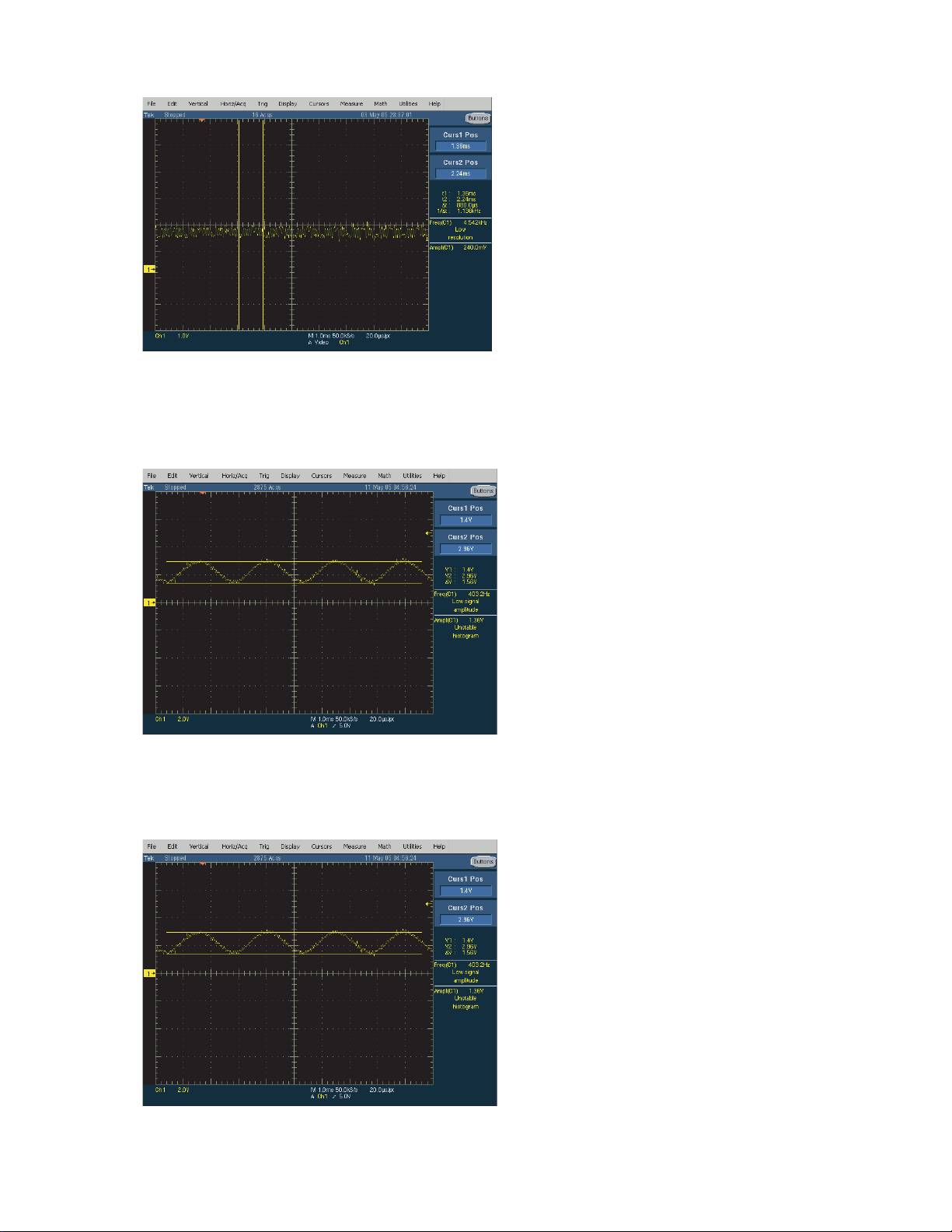
< Waveform 22 >
51
< Waveform 20 >
< Waveform 21 >
Page 52
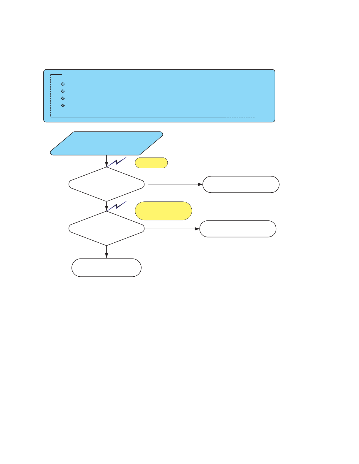
11. No Caption
52
Preliminary Checkpoints
Check the back Solding state in 96 pin connector(JP12(Digital),JP701(DTT&Analog))
Check the CC_RD,GD,BD,FB,VD,HD signal in I C.
Check the I2C between Micom and uPD64012 or EEPROM.
Check the Flash Memory or SDRAM.
CC in Remocon is
O.K. but the CC Does
Not display
OK
Check the Micom_CVBS
(Pin 121)
of IC SDA6001(U29)
OK
Check CC_R,G,B,FB,H,V-sync
of IC SDA6001(U29)
OK
Change the uPD64012
Waveform 23
NG
Waveform 24
R,G,B,FB,H-sync
V-sync
NG
Check Micom CVBS
Connection part
Check the crystal(X2)
and related parts on U29
Page 53
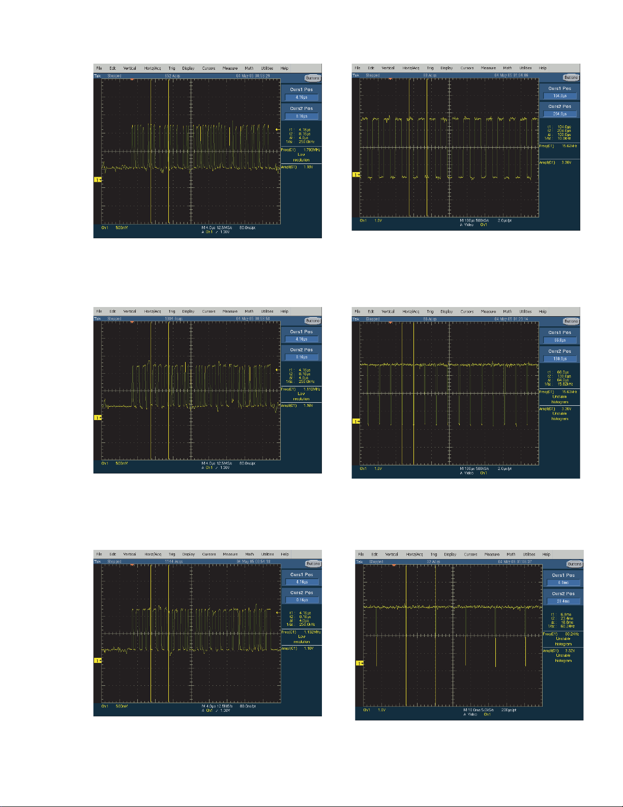
< Waveform 24 R >
53
< Waveform 24 FB >
< Waveform 24 G >
< Waveform 24 B >
< Waveform 24 H-sync >
< Waveform 24 V-sync >
Page 54
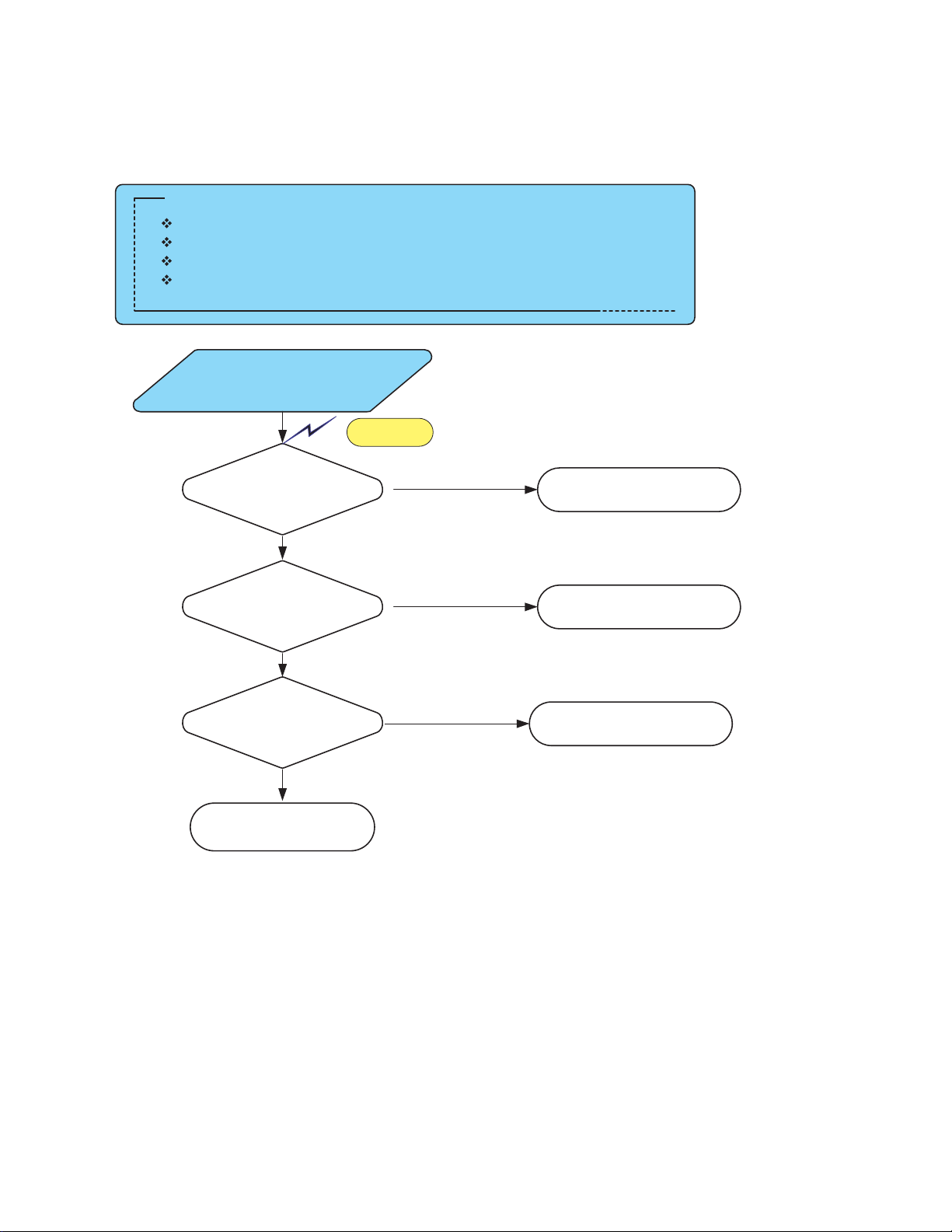
12. Remocon
54
Remocon switch push but the key does not function
Preliminary Checkpoints
Check the Solder state and pin of Connector JP10
Check the Solder state in LED Board.
Check the I2C between Micom and EEPROM.
Check the Flash Memory or SDRAM.
Remocon is O.K. but
the Function does not
operate.
OK
Check the IR Micom(Pin 76)
of IC SDA6001(U29)
OK
Check the Micom part
(IIC Comunication, other
Control line)
OK
When you power
switch off,
the set off
OK
Exchange the Digital Board
Waveform 25
NG
NG
NG
Check Remocon output
and Power in LED Board
Exchange the IC(U29)
Exchange the IC(UP1)
Page 55
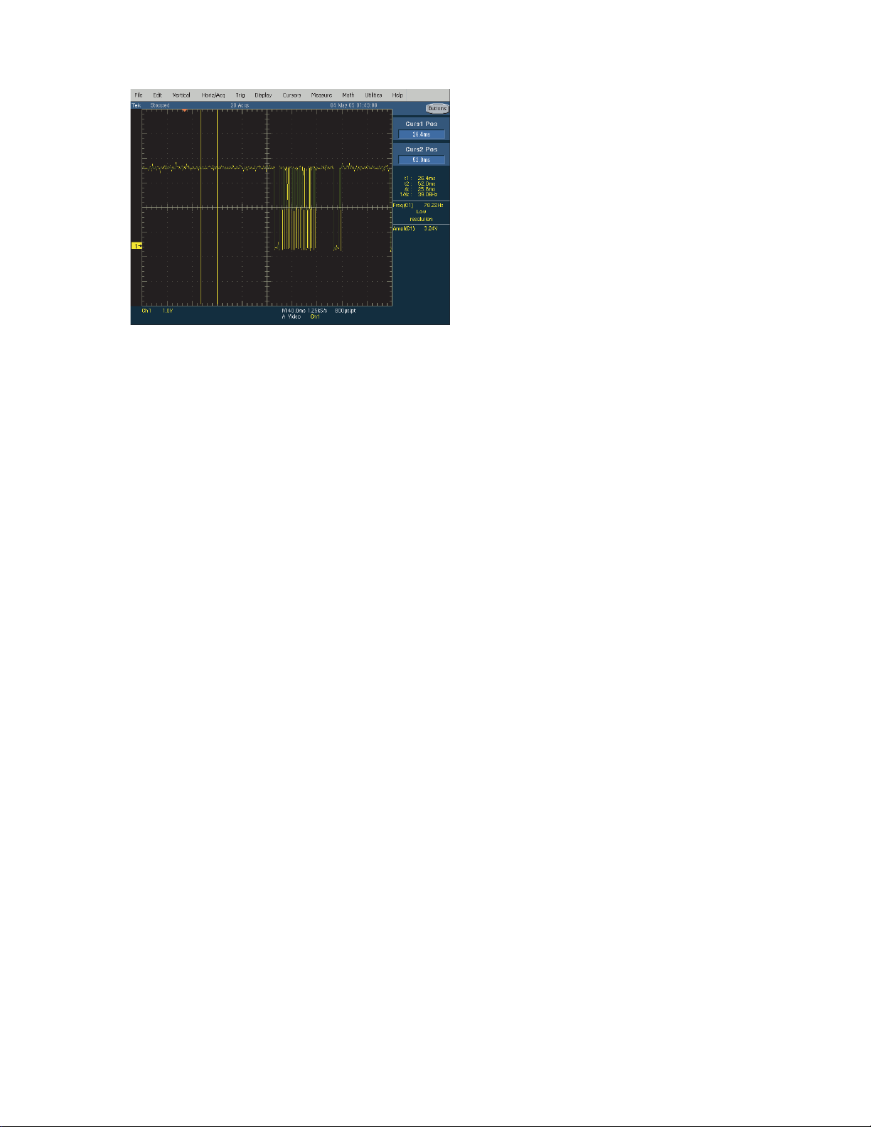
< Waveform 25 >
55
Page 56
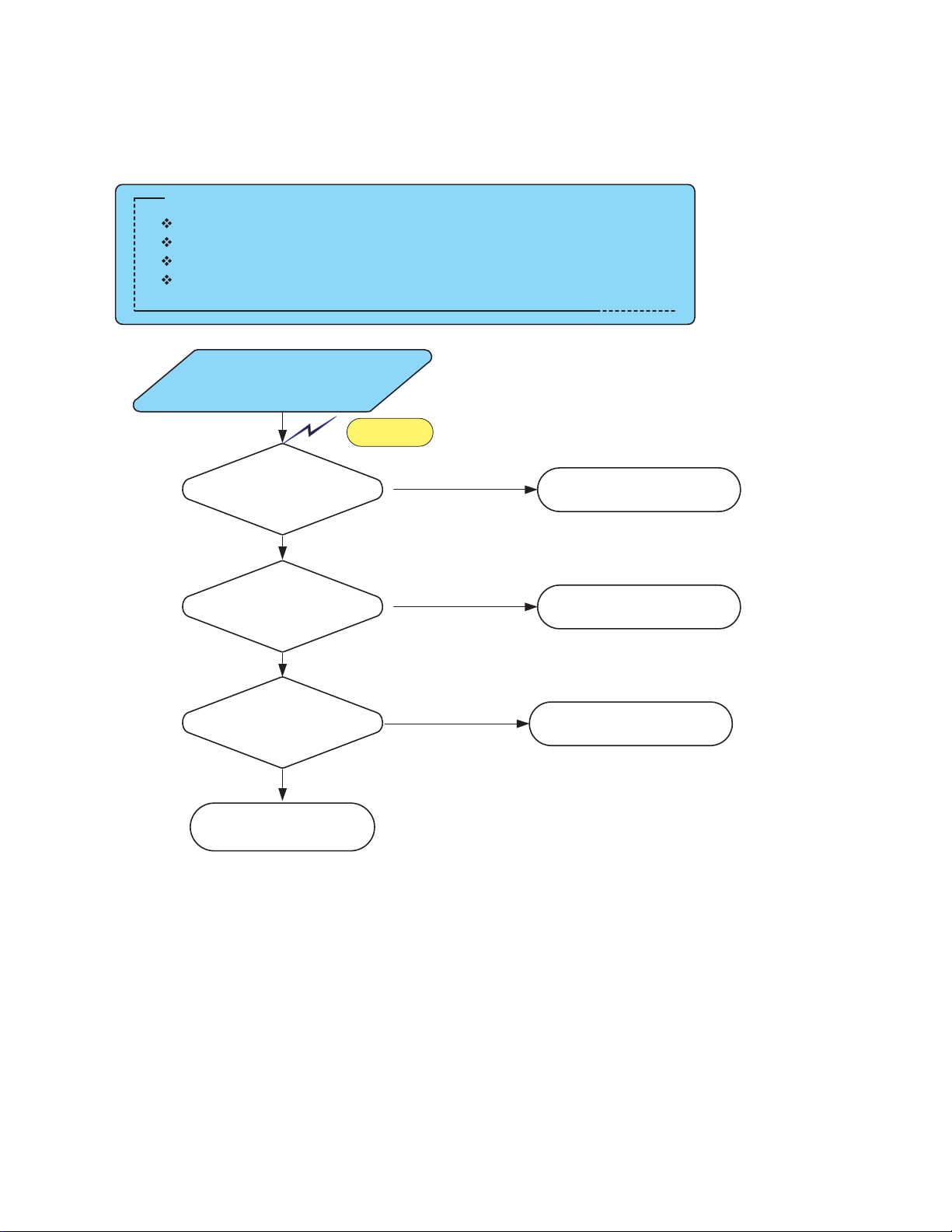
13. Key
56
Key switch is OK but the key does not function
Preliminary Checkpoints
Check the Solder state and pin of Connector JP10
Check the Solder state in Key Board.
Check the I2C between Micom and EEPROM.
Check the Flash Memory or SDRAM.
Control key is O.K. but
the Function does not
operate.
OK
Check the key1,key2
(Pin 124,125)
of IC SDA6001(U29)
OK
Check the Micom part
(IIC Comunication, other
Control line)
OK
Check IR processor
(UP1)
OK
Exchange the Digital Board
Waveform 26
NG
NG
NG
Check Control Key Board
and Power in LED Board
Exchange the IC(U29)
Exchange the IC(UP1)
Page 57
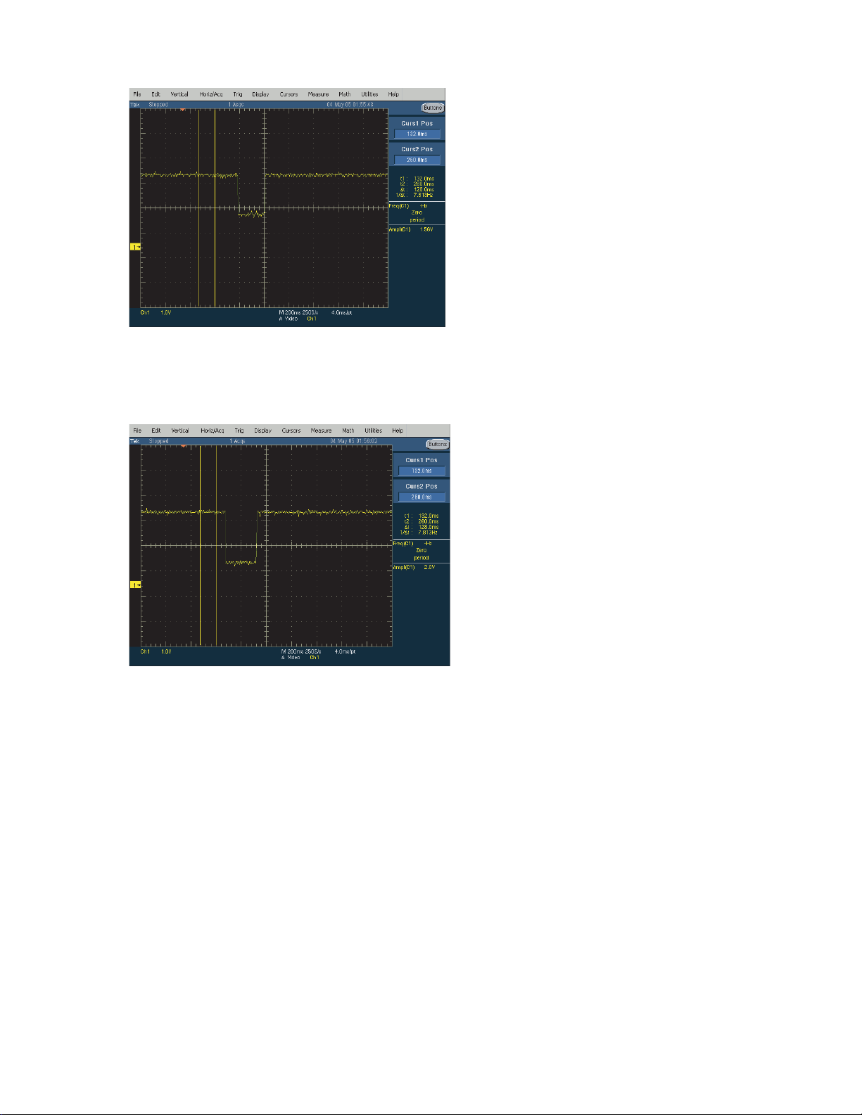
< Waveform 26 >
57
< Waveform 26-1 >
Page 58
DTT Basic Inspection
58
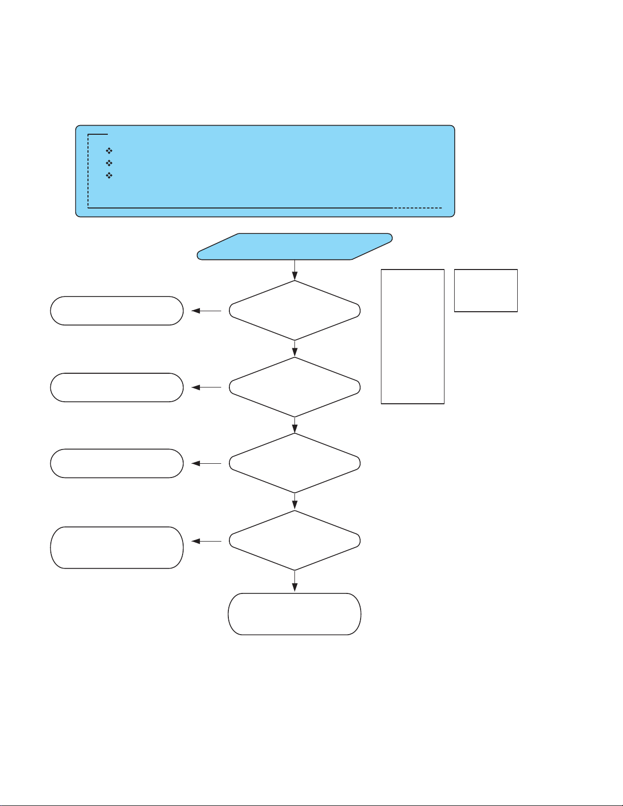
Not Working When Powered On
Preliminary Checkpoints
Check the condition of the input power &cable connection. (JP709)
Check the condition of on-board regulators.
Check for short circuits between each power terminal and the ground.
Check the Digital Board or
SMPS
Perform short circuit test on
each power lines.
NG
NG
Not Working
When Powered On
OK
Check the voltage output
of JP709 & JP701.
OK
Check the voltage output
of JP709 & JP701 after
connecting them.
*JP 709
1. 3.3V
2. 3.3V
3. 3.3V
4. GND
5. GND
6. GND
7. 2.5V
8. 2.5V
9. 2.5V
10. GND
11. GND
12. GND
*JP 701
9. A6VCC
10. A6VCC
OK
Check the power line path
from connector
to on-board regulators.
Check the soldering status of
on-board regulators.
Perform short circuit test on
each power lines.
Note) Please refer to the power diagram of PAU-42THD for detail power connectivity information.
Note) Each input power of DTT comes via the digital board of SMPS directly. So, please check
the digital board prior to SMPS when power input is not working properly.
NG
NG
Check the input voltage
of on-board regulators
OK
Check the output voltage
of on-board regulators
OK
Check the power line path
from on-board regulators
to each components.
Page 59
Basic Inspection
59
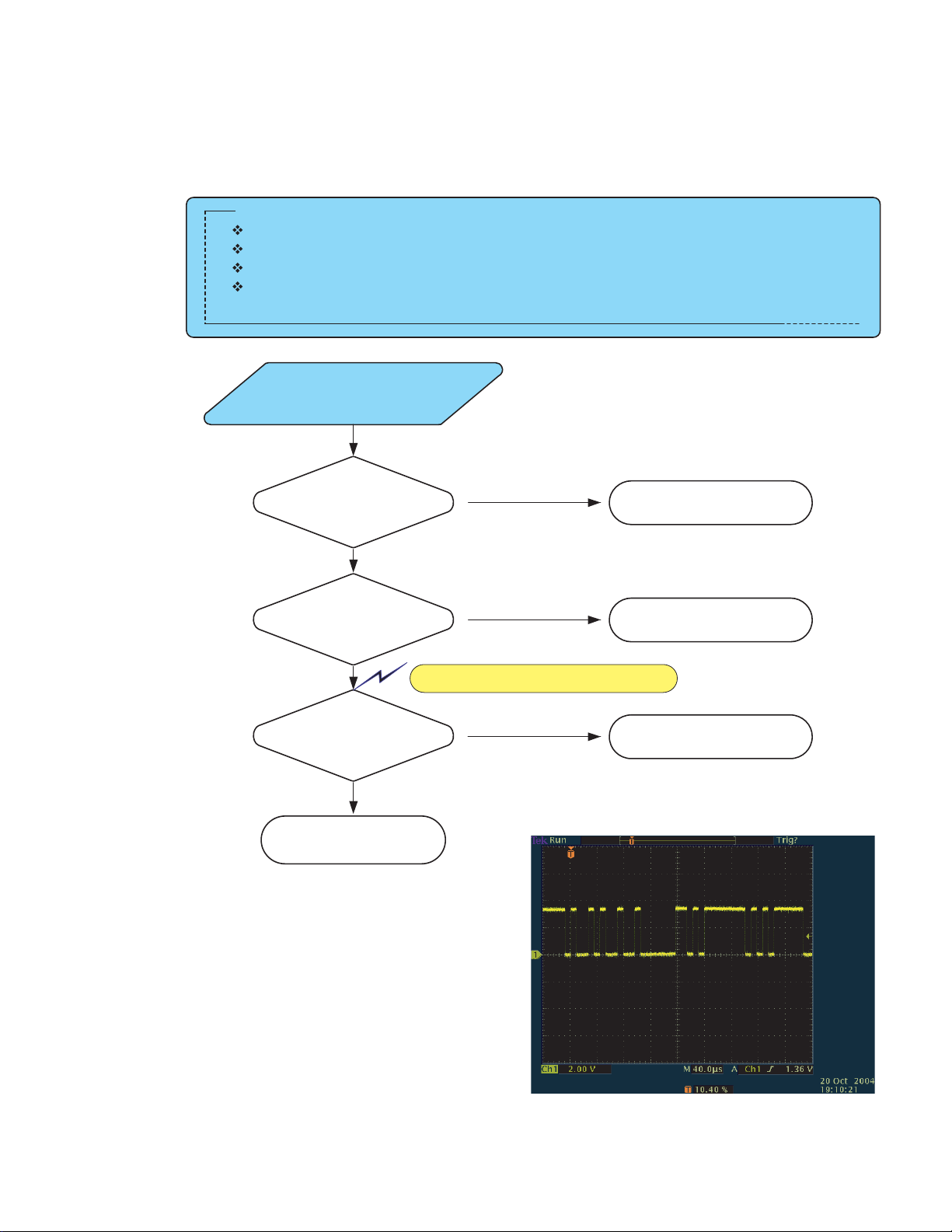
Mulfunction or Not Working of Remote Control Unit
Preliminary Checkpoints
Check the battery condition of the Remote Control Unit.
Check against the a set that works normally to see if the RCU (Remote Control Unit) is working.
Check whether the connector between Digital Board and DTT&Analog Board is connected. (JP701)
Note that DTT board does not receive the key directly from RCU. Instead, MCU of digital board
gets the keys and passes them to DTT through the UART0. (Pin 34 &35 of JP701)
Mulfunction or Not
Working of Remote
Control Unit
Check the battery of the RCU.
Check the RCU.
OK
Check the connector
(JP701)
OK
Check the UART0_RX signal
(Pin 33 of JP701)
OK
Check signal line path to the
main CPU of DTT board
(U2)
Waveform 1 (When 'OK' key is pressed)
NG
NG
NG
Replace the battery/RCU
Secure the connector
Check the digital board /
Check the IR & LED board
< Waveform 1 >
Page 60
Basic Inspection
60
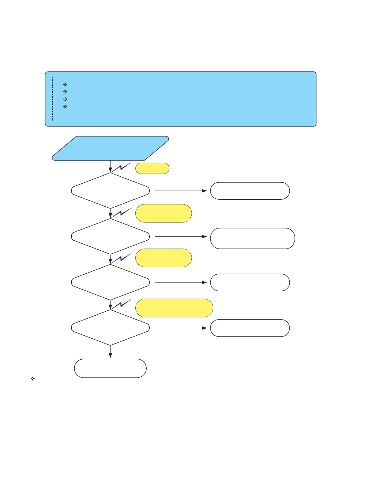
Power Supply is O.K. but the DTT Does Not Wake Up
Preliminary Checkpoints
Check the System Clock (27MHz)and the RESET terminal of CPU.
Check the UART communication terminals between CPU and digital board (UART0).
Check the I2C between CPU and LGDT3303 or EEPROM.
Check the Flash Memory or DDR-SDRAM.
Power Supply is O.K.
but the STB Does Not
Wake up
Waveform 2
Check the System
Clock 27MHz (Pin 15) of IC
MK2475-33G (U261)
OK
Check DDR-SDRAM Clock
(Pin 45 and 46) of DDR-SDRAM
(U5, U6, U7 and U8)
OK
Check system reset of Pin1 on
U281
OK
Check RESET, CS and OE
signals of Flash Memory
OK
Ch:CLK, Ch2:CLK~
Ch:3.3V, Ch2:Reset
Ch1:Reset, Ch2:CS/ Ch3:OE/
Waveform 3
Waveform 4
Waveform 5
NG
NG
NG
NG
Check X-Tal(Y261) and
related parts
Check the Vref and VTT voltage
and clock of
DDR-SDRAM or related parts
Check the soldering state of
U281 or Replace U281
Check Flash Memory
(U40) or related parts
Check for other defective
modes
Useful Tips
1. An Unstable 27 MHz clock may be due to defect of X-TAL or clock generator (U261). Replace the X-Tal or U261.
2. DDR-SDRAM have difference clock inputs which are positive and others are negative signal (Double Data Rate).
3. Vref and VTT are have Vcc/2 and check the power source whether defected.
4. When replacing parts, be cearful of static charges from the tip of the solder iron that can easily damage the parts.
Also, check for assembly condition, soldering condition, or for incorrect or reverse insertion of parts.
5. If the problems are caused by CPU, change CPU board and download Serial Number.
Page 61
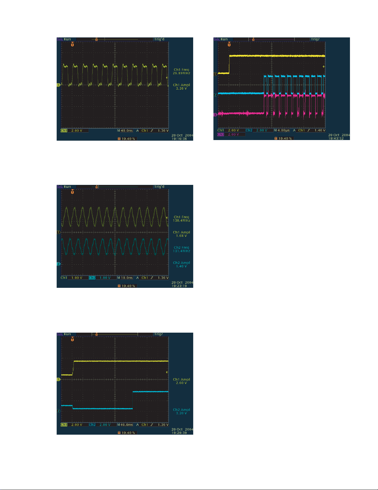
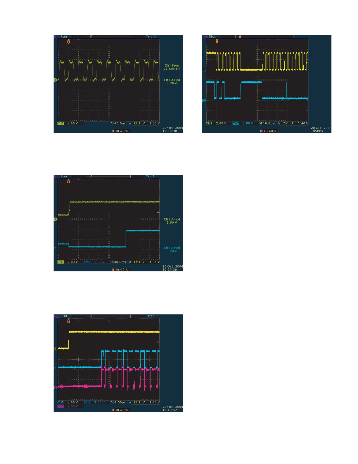
< Waveform 2 > < Waveform 5 >
61
< Waveform 3 >
< Waveform 4 >
Page 62
Basic Inspection
62
Does Not Boot after Power-On or System Reset
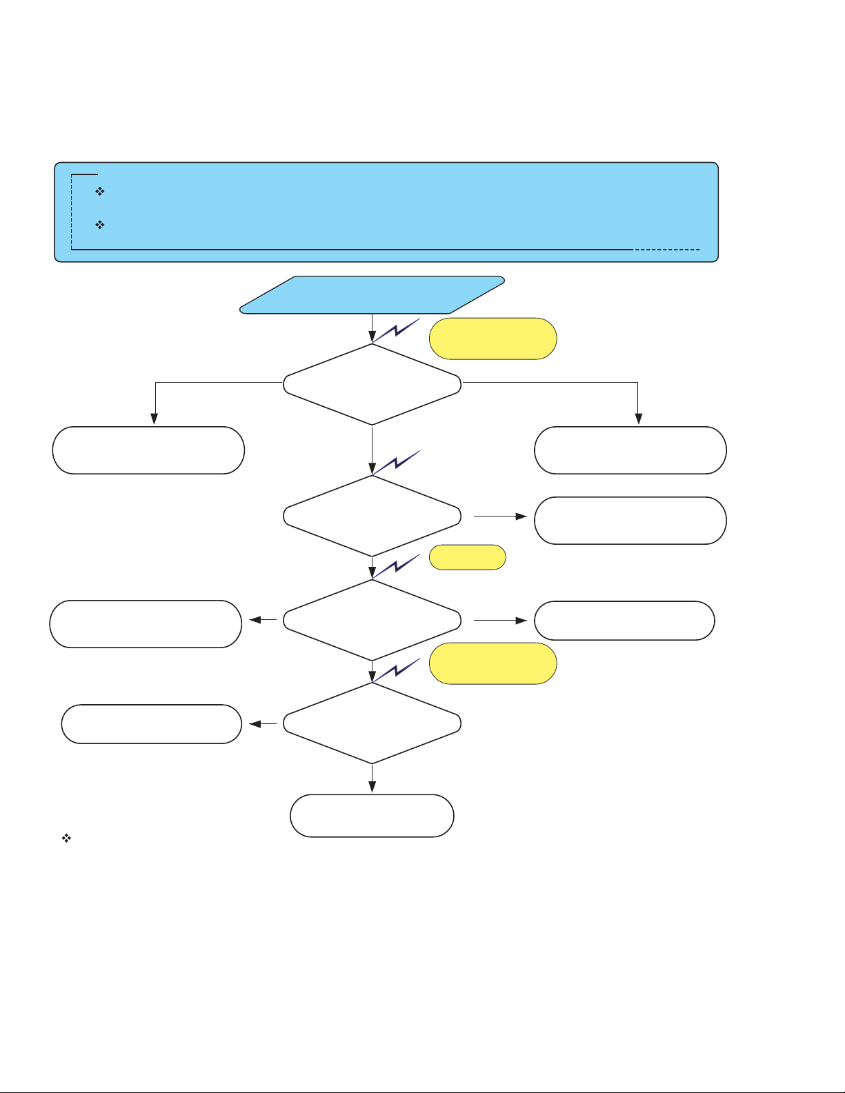
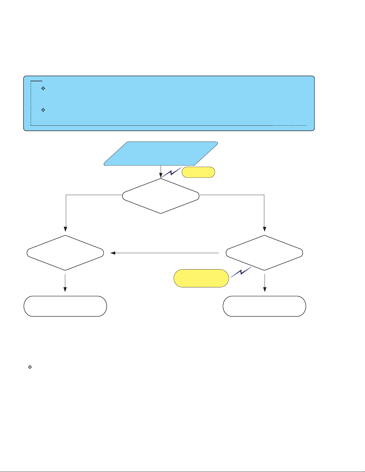
Preliminary Checkpoints
The system clock 27MHz must be stable during the System Reset or the Power On Reset.
However, if X-TAL is defective, the clock may not become stable until RESET is released.
To check reset timing, turn the main power off and back on, and check if the following waveform is maintained.
System/Power-On Reset
Does Not Boot after
Check the Reset and
clock timing of CPU
Waveform 2
Waveform 4
27 MHz Clock problemReset timing promlem
Check the reset signal of
Flash and Pin1 of U281
Check the soldering status
of U40(Flash Memory)
and U62
Check the soldering state of
EFPROM
Useful Tips
NG
NG
OK
Check the communication
between DTT and
digital board
OK
Check Flash Memory
OK
Check the 12C Line
(Pin 6, 5 of U31)
OK
Check for other defective
modes
Waveform 5
NG
NG
Waveform 6
Ch1:SLC, Ch2:SDA
Check the soldering status
of X-TAL(Y261) and U261
Check the soldering status
of JP282.
Check the digital board
Check the waveform CS
and OE of Flash Memory
1. The CPU have two 12C for system controller.
One is communicate with system 12C(TDA10046) and the other is communicate with serial EFPROM for storing data.
2. When the system will not operate even though the basic inspection results were normal, check Flash Memory which
contains channel data and program contents.
3. Additionally check for Local DATA and Local ADDRESS buses between CPU and Flash Memory.
4. When replacing parts, be careful of static changes from the tip of the solder iron that can easily damage the parts.
Also, check for assembly condition, soldering condition, or for incorrect or reverse insertion of parts.
5. If the problems are caused by CPU, change CPU board and download Serial Number.
Page 63
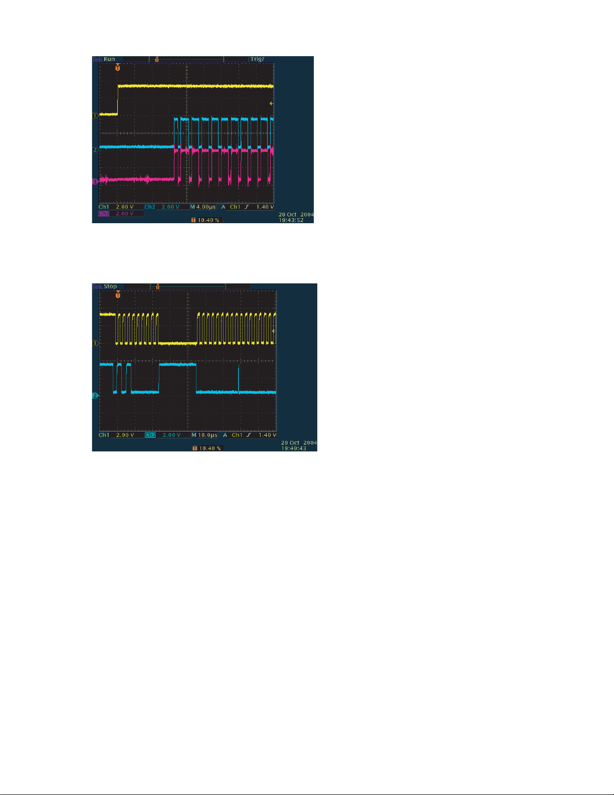
< Waveform 2 > < Waveform 6 >
63
< Waveform 4 >
< Waveform 5 >
Page 64
CPU / SYSTEM MEMORY INSPECTION
64
CPU /System Memory Inspection
Error Occurs During S/W Installation or Update through BOOTROM Board.
System Stops During Initial Booting or Operation.
Preliminary Checkpoints
If the system does not respond even though no problem was found after basic inspection,
you need to check the flash memory that contains program codes for the proper system operation,
Flash Memory Control signals that look similar to below waveforms will be repeated.
The main cause of the problems related to System Memory (i.e.Flash and DDRSDRAM)is the soldering of parts.
Therefore, first check the soldering condition and the power supply of IC.
Error Occurs During S/W
Installation or Update
through BOOTROM Board.
Waveform 5
NG OK
Check CPU
and Flash Memory
(Incorrect insertion, poor
soldering, etc.)
OK OK
Re-check the basic inspection
items
Check Flash Access
signal CE(Pin 14), OE(Pin 54)
NG
Waveform 7
Ch:DDR0A0
CH:DDR0D0
Check the Data and
Addresses of DDR-SDRAM
Check for other defective
modes
Useful Tips
1. Check CE, OE and WE of Flash Memory when system does not operate or cannnot update for new software.
2. When the system will not operate even though the basic inspection results were normal, check Flash Memory which
contains channel data and program contents.
3. Additionally check for Local ADDRESS buses between CPU and Flash Memory.
4. Check the Memory interface of DDRSDRAM if the Flash Memory is not defected.
5. When replacing parts, be careful of static charges from the tip of the solder iron that can easily damage the parts.
Also, check for assembly condition, soldering condition, or for incorrect or reverse insertion of parts.
6. If the problems are caused by CPU, change CPU board and download Serial Number.
Page 65
< Waveform 5 >
65
< Waveform 7 >
Page 66
MPEG INSPECTION
66
MPEG Inspection
No problems Found during Basic and CPU/System Memory Inspections, but MPEG Does Not Play.
- Check DDR SDRAM Interface/Transport Stream(TS).
Preliminary Checkpoints
If the system does not respond even though no problems were found during the basic inspection
and the CPU/Flash inspection, you will need to check the DDR-SDRAM interface.
Check control lines between DDR-SDRAM and CPU also data/address lines.
The main cause of the problems related to System Memory (i.e.Flash and DDR-SDRAM)is the soldering of parts.
Therefore, in the event of a problem, first check the condition of the soldering and the power supply of IC.
No problems Found on
during Basic/Memory
Inspections but MPEG Play
Does Not Work
Ch1:RAS/, Ch2:CAS/, Ch3:WE/
NG OK
Check the solding
status of DDR-SDRAM
(U5, U6, U7 and U8)
OK OK
Recheck the basic inspevtion
items
Useful Tips
1. Make sure that basic function of the system is normal by checking that the VFD toggles
each time you press the Front power key.
2. Check the interface between CPU and DDR-SDRAM U5, U6, U7 and U8.
The interface is composed of clock(133MHz), address, data and control signals.
3. If all connections are complete, replace the DDR-SDRAM.
4. If the problems are caused by CPU, change CPU board and download Serial Number.
Check the output of DDR
SDRAM control interface
NG
Waveform 8
Check the adress and data lines
of between CPU and DDR-SDRAM
Waveform 7
Check for other defective
modes
< Waveform 7 >
< Waveform 8 >
Page 67
A/ V INSPECTION
67
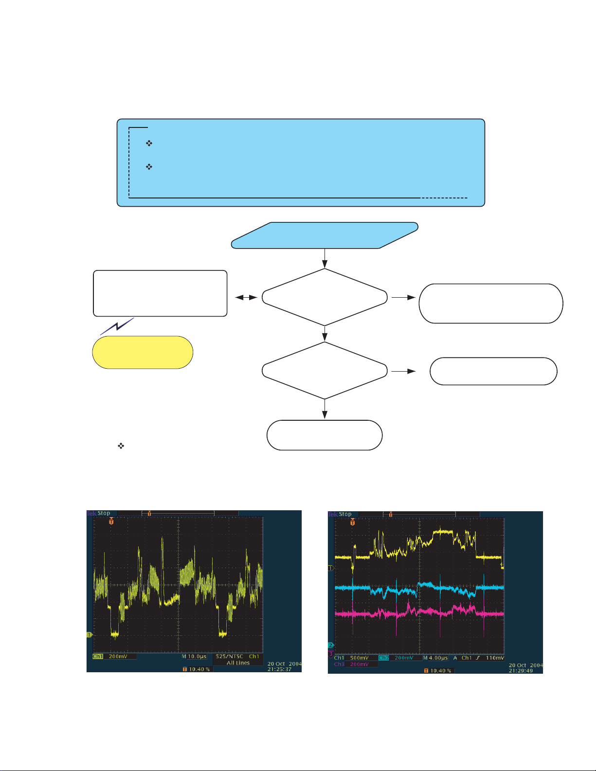
A/V Inspection
No Video Output - CVBS/YPbPr
Preliminary Checkpoints
If no video is output while the UI(User Interface)and key controls are normal,
first check the video output signal of CPU.
If no video signal found,check the TS parallel data between CPU and U531.
If no output of TS data,check the U531 and relevant components.
U2(PIN:A9):CVBS
U2(PIN:B9, C9):
S-VHS
JP141(PIN1, 3, 5,):YPbPr
Waveform 9-1 (CVBS)
Waveform 9-2 (YPbPr)
No video Output
OK
Check the Video output
of CPU
OK
Check the TS line between
CPU and U531
NG
NG
Check the path between
CPU and JP705, JP706 (Incorrect
insertion, poor soldering, short
circuits, damage, etc.)
Check the TS signal path from
tuner to U531.
OK
Check for other defective
Useful Tips
1. If no output of TS data but tuner is good, check the U531 and relevant components.
modes
< Waveform 9-1 >
< Waveform 9-2 >
Page 68
A/V Inspection
68
No Audio Output
Preliminary Checkpoints
If no audio is output through JP800 while the system is normal, first check the
CPU AUDIO output and clock. [I2S interface ].
If no problems were found, check the U671 for Audio DAC.
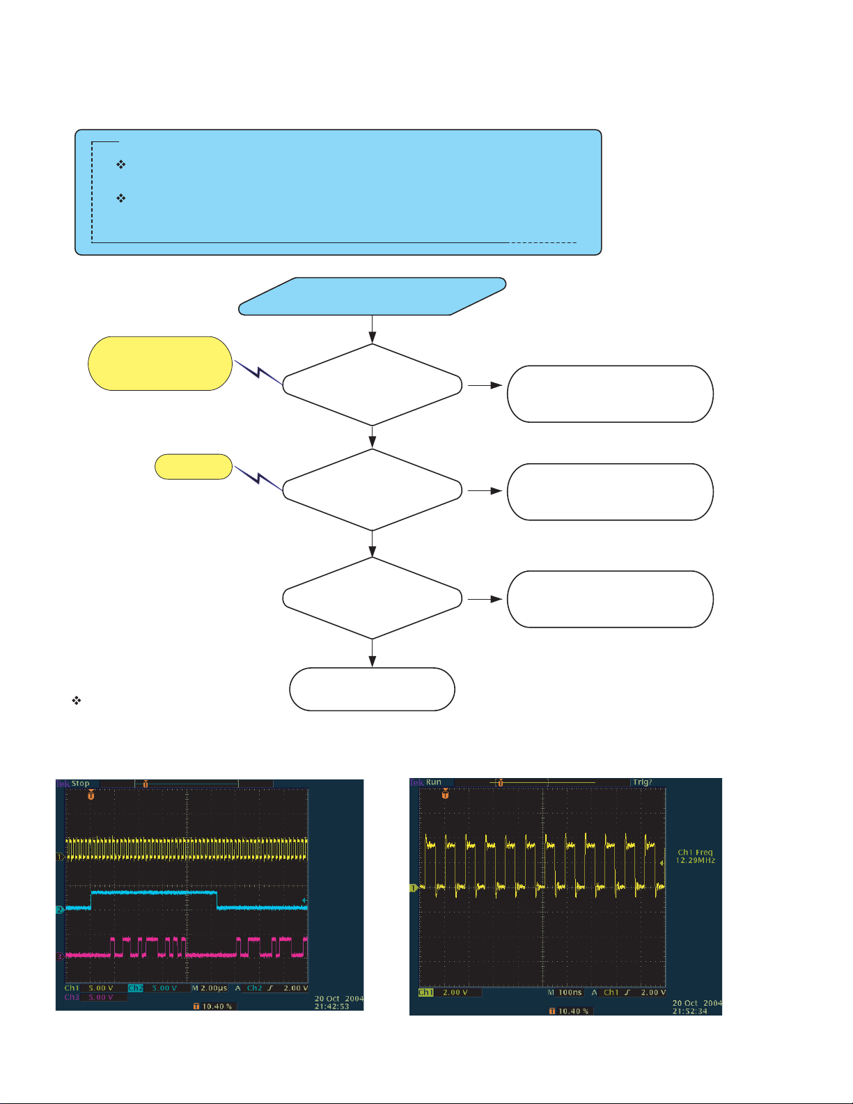
Waveform 10
Ch1:SCLK,
Ch2:LRCLK,
Ch3:ADATA0
No Audio Output
OK
Check the CPU
12S output
OK
NG
Check the path between
CPU and Clock
(Incorrect insertion, poor soldering,
short circuits, damage, etc.)
Waveform 11
Check the Audio clock
Pin 9 of U261
OK
Check the Audio DAC for
Useful Tips
1. The Audio problem largely from the defect of CPU, Audio DAC or incomplete soldering of the parts located along
the audio output path.
2. Audio DAC pins represent serial data, LR clock, Bit clock and system clock, respectively.
U761
OK
Check for other
defective modes
NG
NG
Check the X-TAL and U261
(Incorrect insertion, poor soldering,
short circuits, damage, etc)
Check the path between
Audio DAC and CPU
(Incorrect insertion, poor solding,
short circuits, damage, etc)
< Waveform 10 >
< Waveform 11 >
Page 69
A/V Inspection
69
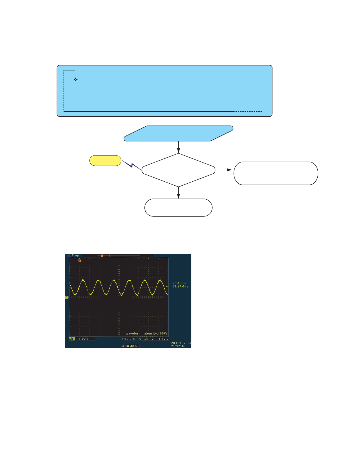
No digital audio output
Preliminary Checkpoints
If the SPDIF output is not working while the system is normal (Including MPEG
play and A/V output), check for any problems with the SPDIF output of CPU.
No IEC958 Digital Output
Waveform 13
Check the IEC958 output
signal J5 of U2
OK
Check for other
defective modes
NG
Check the path between
CPU and IEC958 line
(Incorrect insertion, poor soldering,
short circuits, damage, etc.)
< Waveform 13 >
Page 70
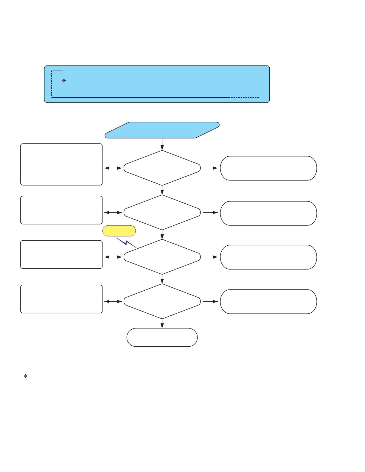
CHANNEL INSPECTION
70
Channel Inspection
No Channel Locking with No Problems with Power/CPU
Preliminary Checkpoints
If channel locking fails even though there is no problems with the system, check
the Interface between Tuner, LGDT3303 and CPU.
Channel locking failure
- LDGT3303 Input Power
* +3.3V
Pin21, 35, 61, 93
* +1.8V
PIN16, 19, 32, 42, 47, 55, 63,
68, 74, 81, 85, 89, 100
Check the LGDT3303
input voltage
NG
After the basic inspection, check the
path between U501 and LGDT3303
(Incorrect insertion, poor soldering,
short circuits, damage, etc)
- LDGT3303 PIN26
* low : reset on
* high : reset release
- LGDT3303 Pin 79, 80
* 25MHz clock
- 12C CLOCK [PIN48]
- 12C DATA[PIN49]
Check the LGDT3303 input
Waveform 14
OK
(Reset) = high
OK
Check the LGDT3303
input clock
OK
Check the 12C control
Check other related
part
NG
NG
NG
Check the path between
CPU and LGDT3303 (Incorrect
insertion, poor soldering, short
circuits, damage, etc.)
Check the path between
LGDT3303 and X-Tal (Incorrect
insertion, poor soldering, short
circuits, damage, etc.)
Check the path between
devices the LGDT3303 and EEPROM
Also, check Incorrect insertion, poor
soldering, short circuits, damage, etc.)
Useful Tips
1. Check the power byU532 are properly provided to the U531.
2. Check the 12C interface between tuner and 10046. If no problem, inspect along the tuner output path to TDA10046.
Whether the components of R, L, C's soldering status.
3. If no problem, replace the Tuner.
4. If the problems are founded by CPU, replace the CPU board and also download SN.
Page 71
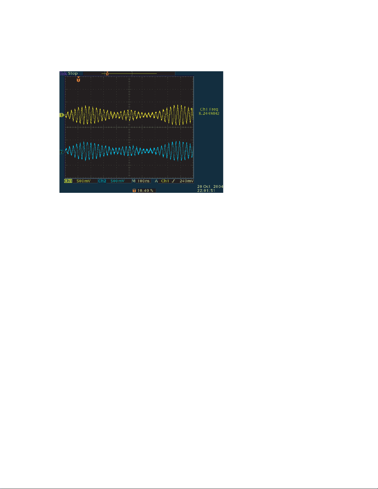
< Waveform 14 >
71
Page 72
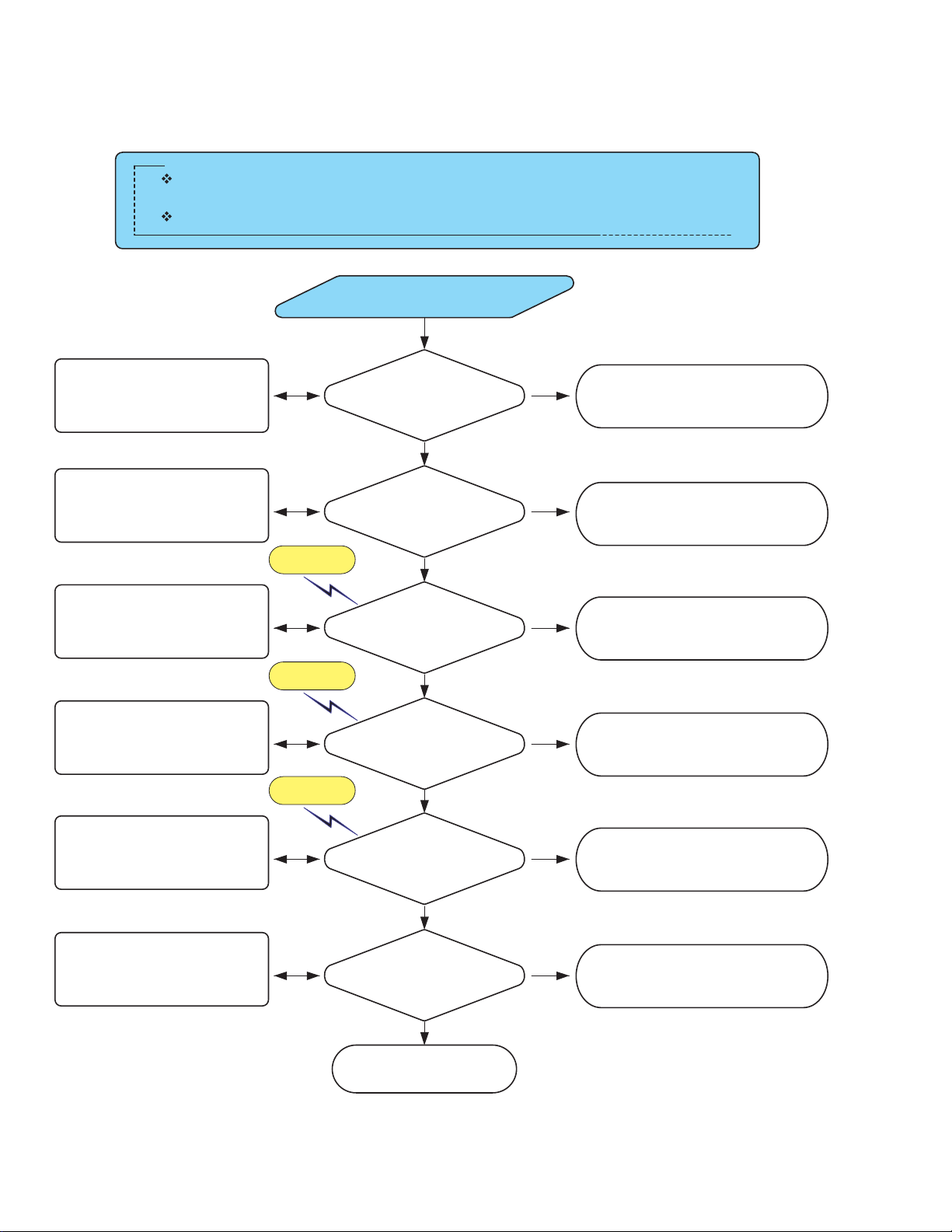
CHANNEL INSPECTION 2
72
Channel Inspection
No Channel Locking with No Problems with Power/CPU
Preliminary Checkpoints
If channel Locking fails even though there is no problems with the system, check
the TUNER 12C BUS and IF signals.
If the Tuner 12C and IF signals are good but cannot search, check TS data goes to CPU
Channel locking failure
* +5VDT of PIN 3, 7
* PIN48 [SCL] of LGDT3303
* PIN49 [SDA] of LGDT3303
* VIN+
* VIN-
* PIN22(TUNER_AGC)
of LGDT3303
Waveform 15
Waveform 16
Waveform 17
Check the TUNER power
OK
Check the 12C DATA and
CLOCK of TUNER
OK
Check the TUNER output
(VIN+, VIN-)
OK
Check the TUNER
AGC
OK
NG
NG
NG
NG
After the basic inspection, check the
path between SMPS and TUNER
(Incorrect insertion, poor soldring, short
circuits, damage, etc)
Check the path between
CPU and LGDT3303 (Incorrect
insertion, poor soldering, short
circuits, damage, etc.)
Check the path between
LGDT3303 and TUNER (Incorrect
insertion, poor soldering, short
circuits, damage, etc.)
Check the path between
LGDT3303 and Tuner
(Incorrect insertion, poor soldering,
short circuits, damage, etc.)
* PIN46(VSB_CLK) of
LGDT3303
high : lock
low : unlock
* VSB_D [7 : 0] of
LGDT3303
Check the output of Pin46
is high, also check clock
and valid of LGDT3303
OK
Check the TS DATA output
and goes to CPU
Check for other defective
modes
NG
NG
Replace the related parts
(demodulator)
Replace the related parts
(demodulator)
Page 73
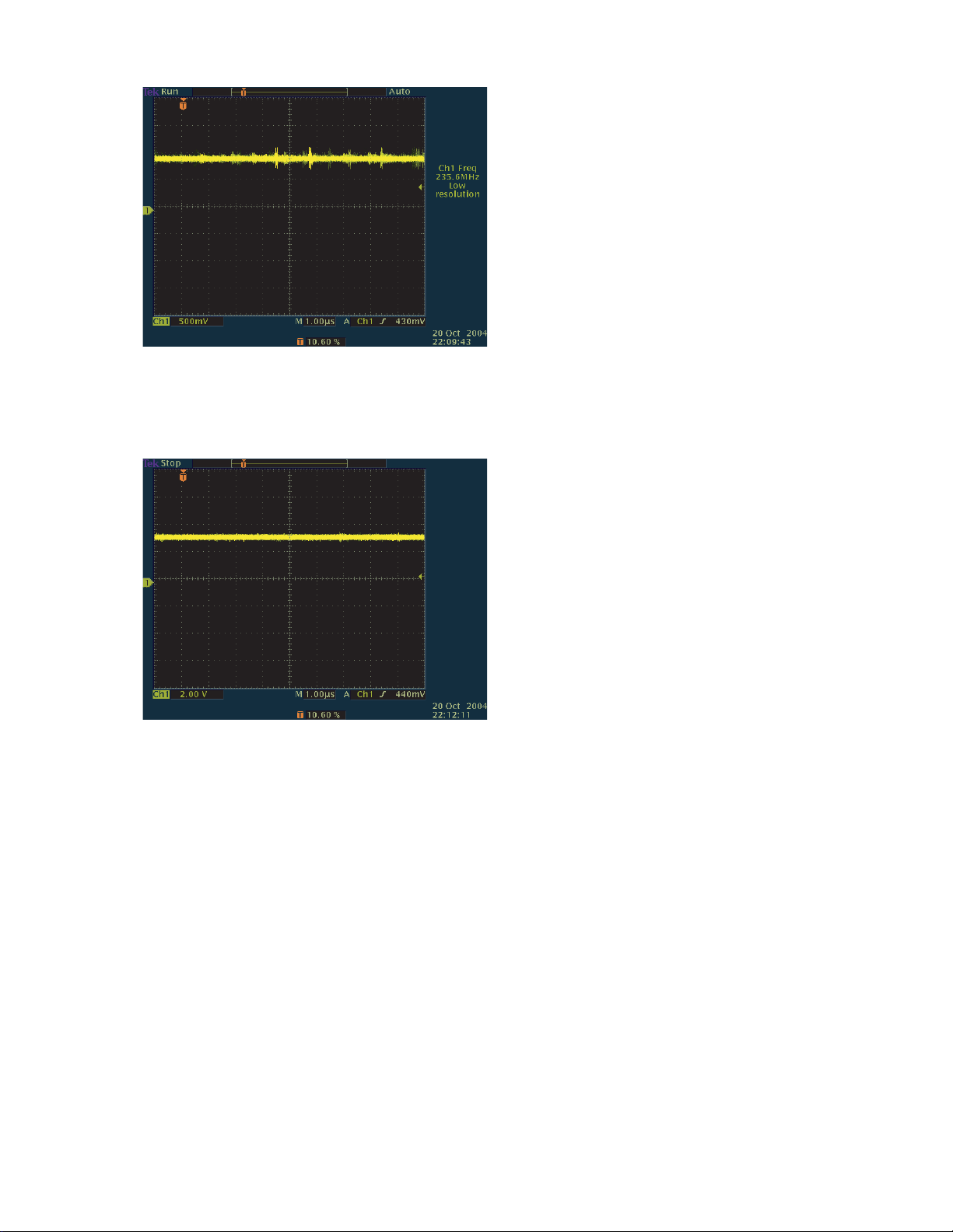
< Waveform 15 >
73
< Waveform 16 >
Page 74
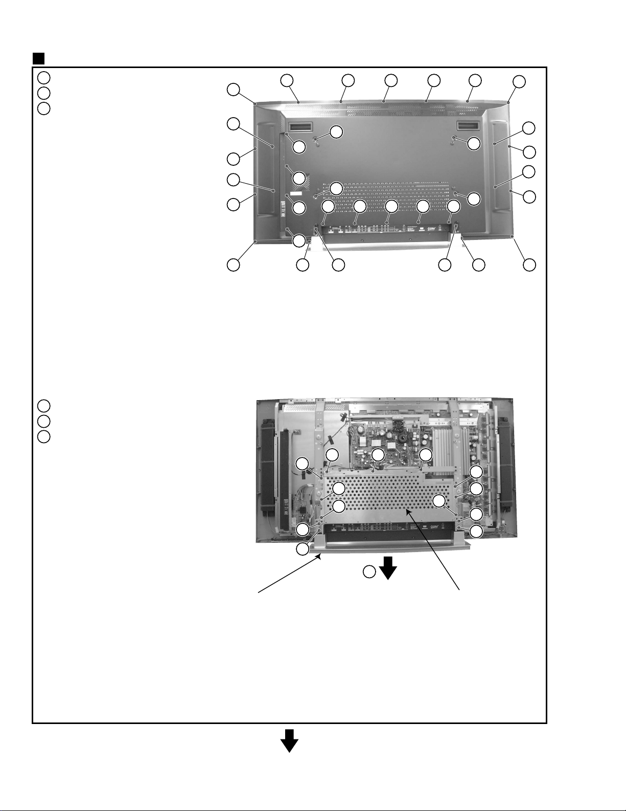
DISASSEMBLY
74
1
Rear Case(42a3HD), Stand and Shield Assys
Remove the 15 screws (T4 x 16).
1
Remove the two screws (M4 x 12).
2
Remove the 17 screws (M4 x 8).
3
1
1 1 1 1 1
3
3
3
3
1
3
3
1
3
1
3
3
1
3 3 3 3 3
3
3
1
3
SHIELD ASSY and STAND ASSY
Remove the nine screws (M3 x 8).
4
Remove the four screws (M4 x 12).
5
Remove the stand.
6
1
4
4 4
12 21
1
4
4
4
4
4
5
4
5
5
5
6
STAND ASSY SHILED ASSY
Page 75
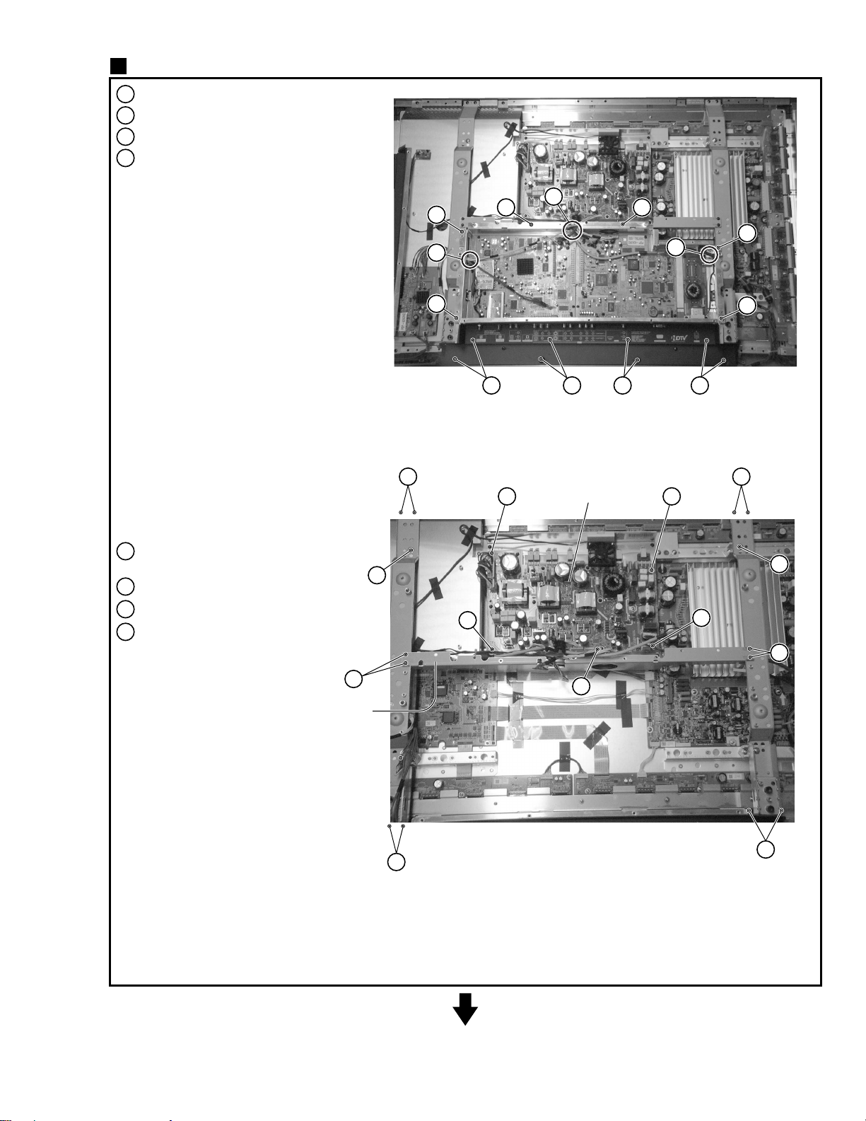
2
75
ANALOG, DIGITAL and EMI FILTER
Remove the six screws (M3 x 8).
7
Remove the eight screws (M4 x 8).
8
Remove the connector (right → center → left).
9
Remove the ANALOG DIGITAL EMI FILTER.
10
Remove the Assy Brkt V-supporter L and R.
Remove the four screws (M3 x 8) to release
11
the ASSY BRKT MAIN.
Remove the four screws (M5 x 12).
12
Remove the eight screws (T4 x 16).
13
Remove the five screws (M3 x 8) to release
14
the SMPS.
12
13
7
7
9
7
7
9
7
8
8 8 8
9
7
13
14
SMPS
14
12
14
14
11
11
ASSY BRKT MAIN
14
13
13
Page 76
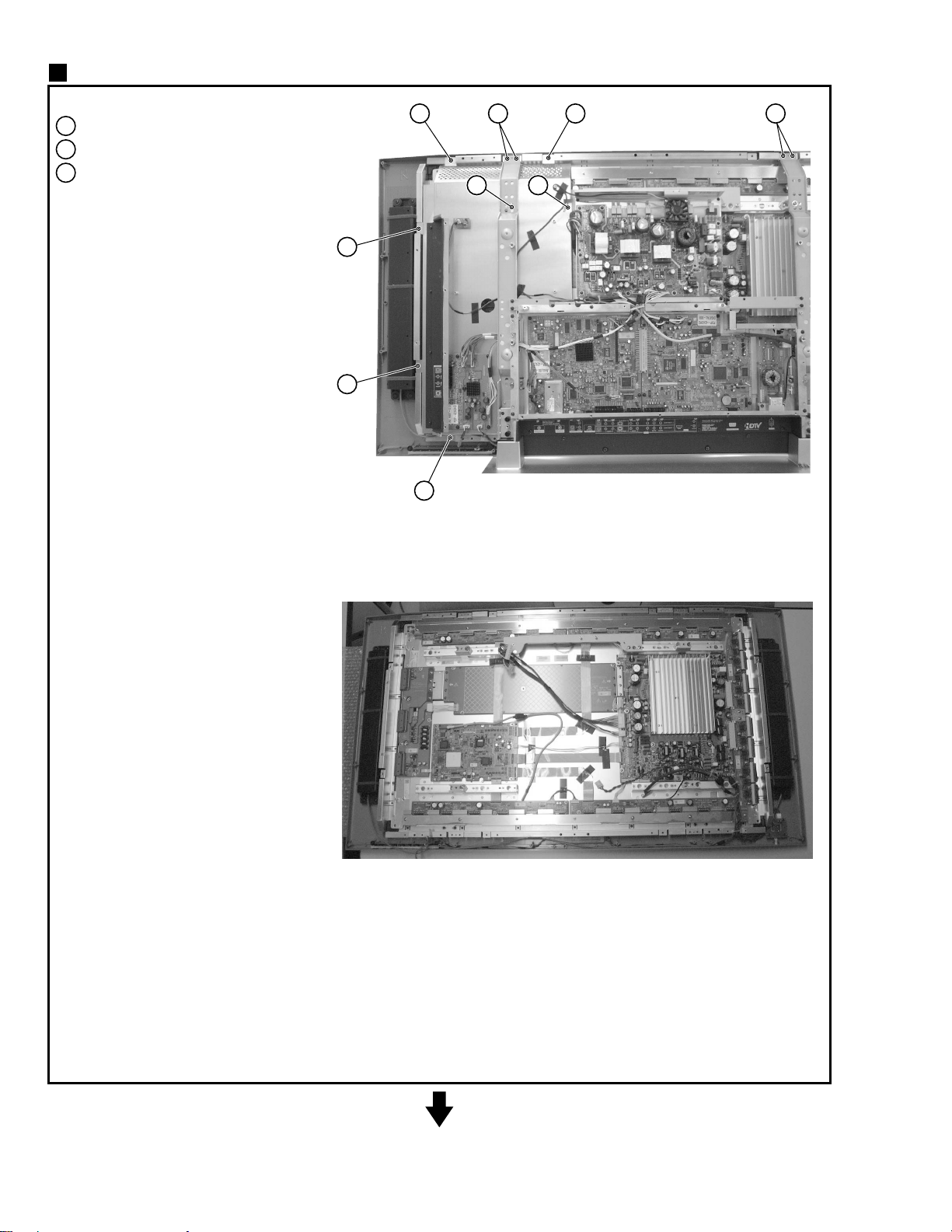
3
76
SHIELD SIDE
Remove the SHIELD SIDE
Remove the three screws (T4 x 16).
15
Remove the screw (M4 x 10).
16
Remove the three screws (M4 x 8).
17
17
17
15
15
17 16
1513
13
PDP PANEL
Page 77
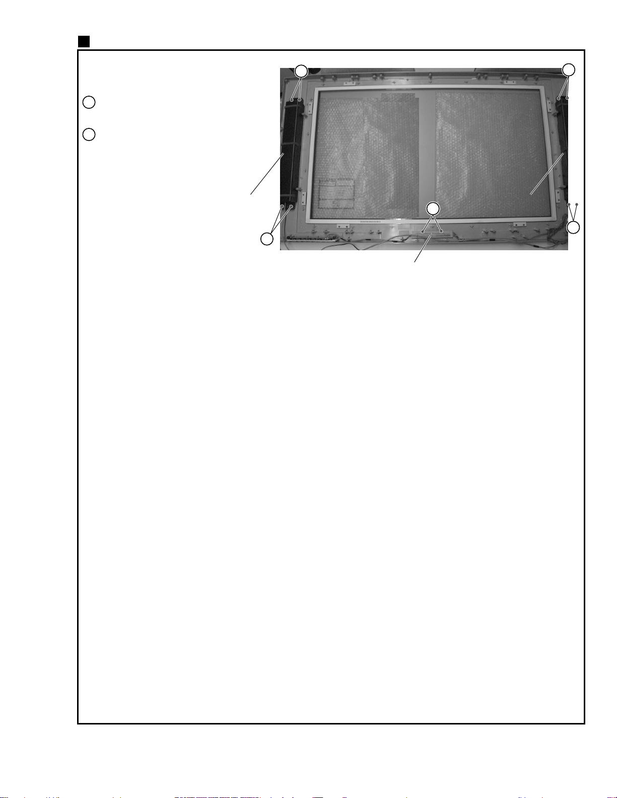
4
77
SPEAKERS
LED PCB
Remove the two screws to release the LED PCB.
18
Remove the eight screws (T4 x 14) to
20
release the SPEAKER L/R.
SPEAKER R SPEAKER L
20
20
20
18
20
Page 78

HOW TO DIAGNOSE THE PDP MODULE
78
HOW TO DIAGNOSE THE PDP MODULE
(PDP-NP42H5MF01PA/PB)
1. List of tools required for repair
2. Points of failure diagnosis for a Board Assy (PKG)
3. Replacement method of a Board Assy (PKG)
and notes on replacement
4. Adjustments after replacement of parts in the module
5. Operation check
1. List of tools required for repair
a) Phillips screwdriver:For detaching/reattaching PKGs
b) Antistatic wrist strap:
To be used when electronic components, such as PKGs, are to be handled
c) Signal generator (PC, etc.) :For voltage adjustment and display check
d)DVM:For voltage adjustment.
f)DVMTester:For cable check, voltage adjustment, etc.
g) Cushion:To be used when the PKGs are to be replaced
Note: Be sure to wear a wrist strap when you detach/reattach PKGs (Board Assy) to protect
electronic components from being damaged by electrostatic charges.
Page 79
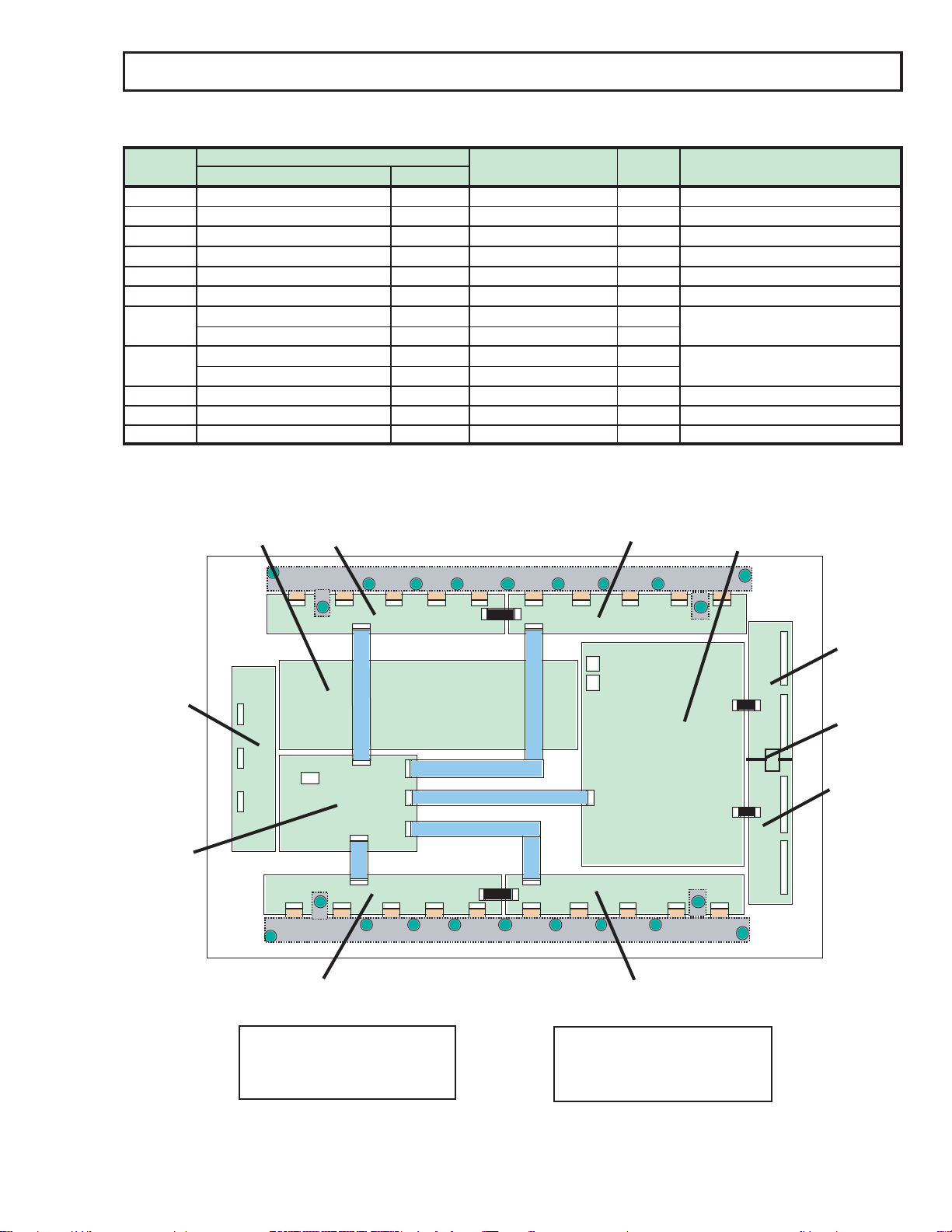
PARTS LIST
L
79
NP42H5MF01PA/PB
SYMBO
PKG42H5G1 03B 9S899891
1
PKG42H5C1 17C-08 9S890002
2
PKG42H5J7 02A 9S899895
3
PKG42H5J8 02A 9S899896
4
PKG42H5J5 02A 9S899893
5
PKG42H5J6 02A 9S899894
6
PKG42H5E1 02A 9S899897
7
PKG42H5E1 02C 9S899862
PKG42H5E2 02A 9S899898
8
PKG42H5E2 02C 9S899863
10
11
12
PKG42H5E3/50X6E3 02A 9S899899
PKG42H5J4 02A 9S899919
PKG42H5J3 02A 9S899918
Notes: • The version of a board assy (PKG) is indicated on the label on the board assy.
TYPE NAME VERSION
• When replacing the scanning relay board assys (PKG-C), make sure that the PKG-U
and PKG-D of the same version are used, to ensure correct scanning timing.
PART NAME
PART NO
QTY
1
1
1
1
1
1
1
1
1
1
1
1
1
NOTE
High Voltage Board
Digital Board
Data Relay Board(Left Down)
Data Relay Board(Right Down)
Data Relay Board(Left Up)
Data Relay Board(Right Up)
Scan Relay Board(Up)
Scan Relay Board(Down)
Scan Relay Board(Center)
Common Connection Board
Common Relay Board
11
12
5
Data Relay (Left up)
Data Relay (Right up)
6
1
Scan Relay Board
(Up)
7
Common Relay Board
10
High Voltage Board
Common Connection
Digital Board
8
2
Data Relay Board (left)
Data Relay Board (right)
Scan Relay Board
(Down)
3
Version label of the board assy (PKG)
• Part name
• Serial number
• HW version • SW version
Digital PKG
• Part name
• Serial number
• Version number
Other PKG
4
Page 80
Compatible table of the board version
80
NP42H5MF01PA/PB
Upper compatible if no terms.
Name of (board) Version Replaceable Version
High Voltage Board
PKG42H5G1
03B
NoteConditions
03B
Common Connection Board
PKG42H5J4
Data Relay Board(Left Down)
PKG42H5J7
Data Relay Board(Right Down)
PKG42H5J8
Data Relay Board(Left Up)
PKG42H5J5
Data Relay Board(Right Up)
PKG42H5J6
Common Relay Board
PKG42H5J3
Scan Relay Board(Center)
PKG42H5E3/50X6E3
Scan Relay Board(Up)
PKG42H5E1
Scan Relay Board(Down)
PKG42H5E2
Digital Board
PKG42H5C1
01A
02A
01A
02A
01A
02A
01A
02A
01A
02A
01A
02A
01A
02A
01A
02A
01A
02C
01A
02A
01C
02C
01C-07/02C-07
11C-07/12C-07
13C-07
14C-07
12C-08
14C-08
15C-08
16C-08
17C-08
01A/02A
01A/02A
01A/02A
01A/02A
01A/02A
01A/02A
01A/02A
01A/02A
01C/02C
01A/02A
01C/02C
17C-08
Scan Relay Board(up) should be combined with the same version
of Scan Relay Board(Down) .
Scan Relay Board(Down) should be combined with the same
version of Scan Relay Board(Up).
Page 81
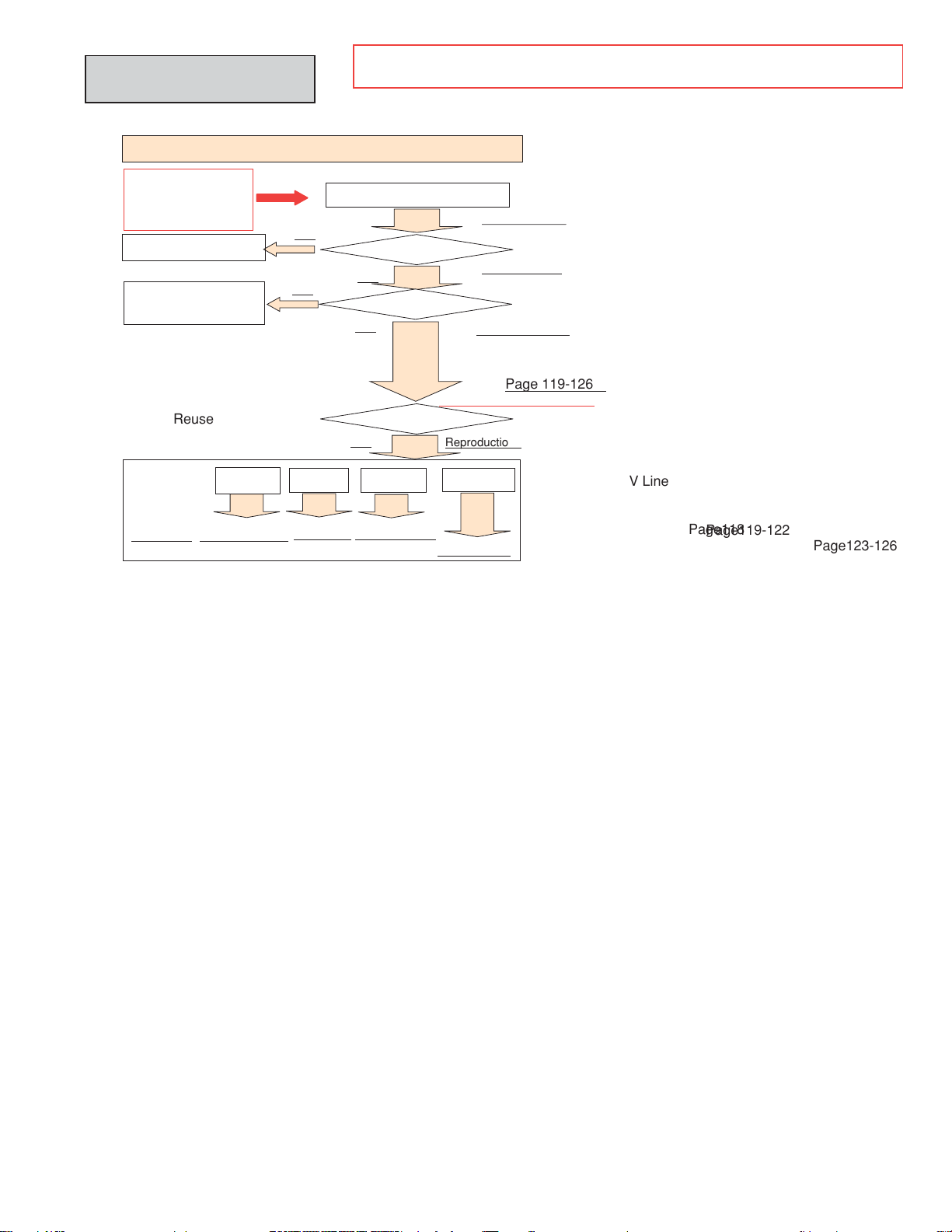
Follow the procedure below for failure diagnosis. Keep wearing Antistatic wrist Band
81
H Line
TROUBLE SHOOTING
until all work and testing has finished.
Procedure FOR BASIC Service TROUBLE SHOOTING
From Service
Manual of the
product
Exchange PDP
Reconnect or
exchange
Reuse
V Line
Page 87
NG
NG
H Line
Model, Serial No. and Panel ID.
Page 82 (1)
Panel Crack
OK
Connectors/Cables
OK
Page 82 (2)
Page 83 - 85
(Page 87-92)
Phenomenon
NG
Picture
Reproductio
Power-off
Page 91
Page 92-95
Page 119-126
V Line
Page118
Page119-122
Page123-126
Page 82
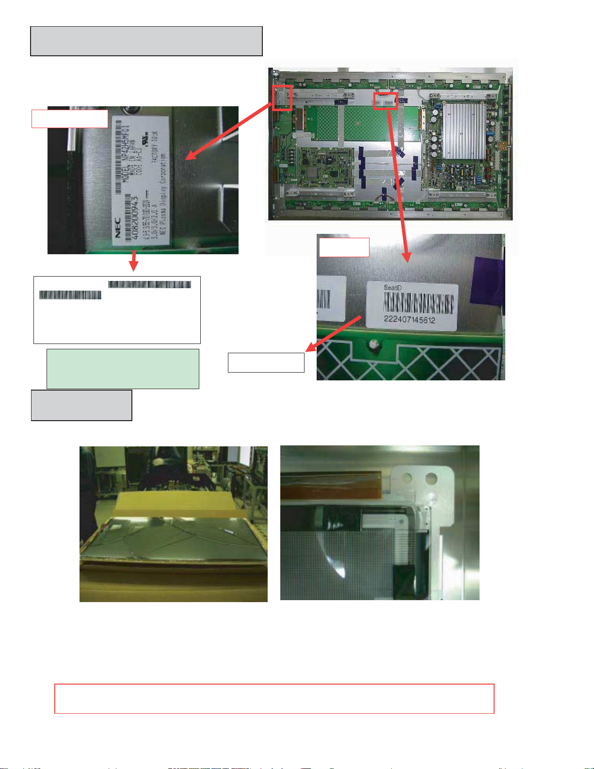
(1) Model, Serial No., and Panel ID
82
Exercise Caution when moving a product with damaged glass.
Refer to the photographs below to find Model,
Serial No. and Panel ID.
Model/Serial No.
Panel ID
NEC
MODEL NP42H5MF01
408200943 MADE IN JAPAN
CODE AA-C3
NEC Plasma Display Corporation
Above Example
Model:NP42H5MF01AA
Serial No.: 408200943
(2) Panel Crack
Refer to the photographs below to check panel for crack.
222407145612
Panel may be cracked due to handling during or after transportation.
Page 83
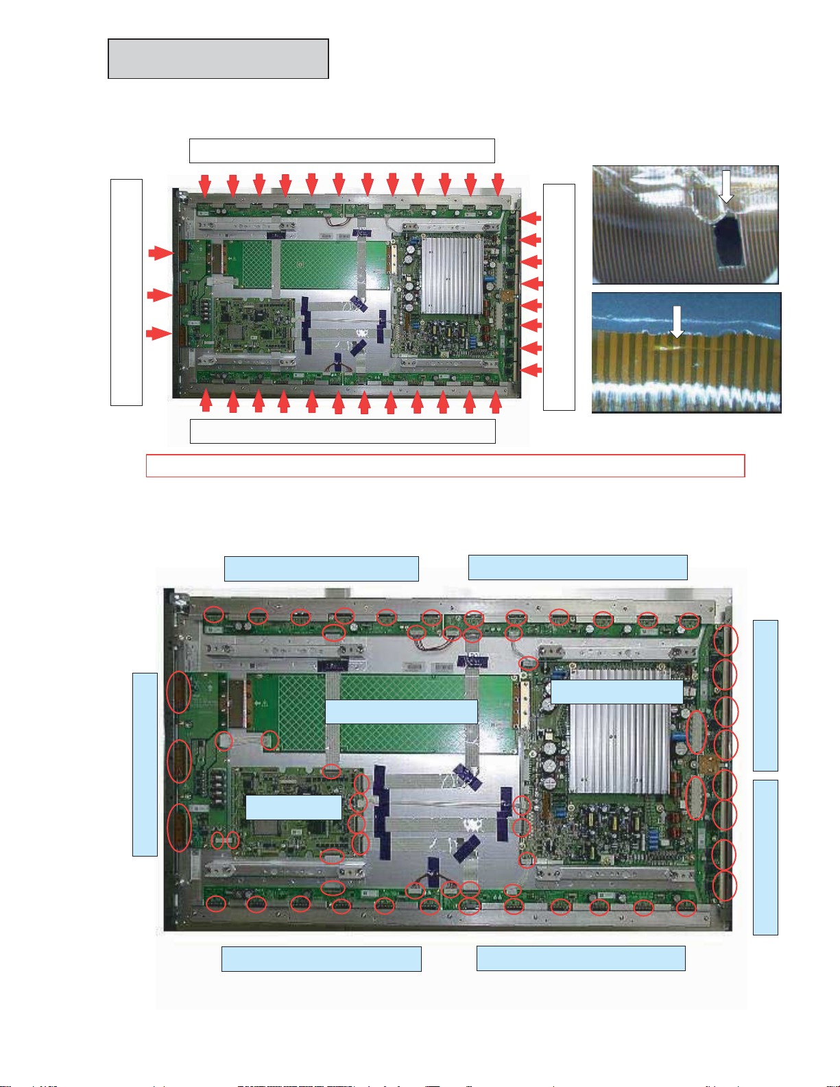
(3) Connectors/Cables
83
(3-1) Check connectors and cables for breakage or disconnection referring to the photos below.
Data Relay Flexible Cable (UP)
Common Voltage Flexible Cable
Data Relay Flexible Cable (Down)
Scan Voltage Flexible Cable
(Caution) Take care for the cable handling. Careless handling inproduction line may cause this Failure.
(3-2) Check connectors and cables whether they are connected and locked right.
See Page 114-115 for the right procedure of connection.
Data Relay Board (LU)
Common Relay Board
Digital Board
Common Connection Board
Data Relay Board (RU)
High Voltage Board
Data Relay Board (LD)
Scan Relay Board (D) Scan Relay Board(U)
Data Relay Board (RD)
Page 84
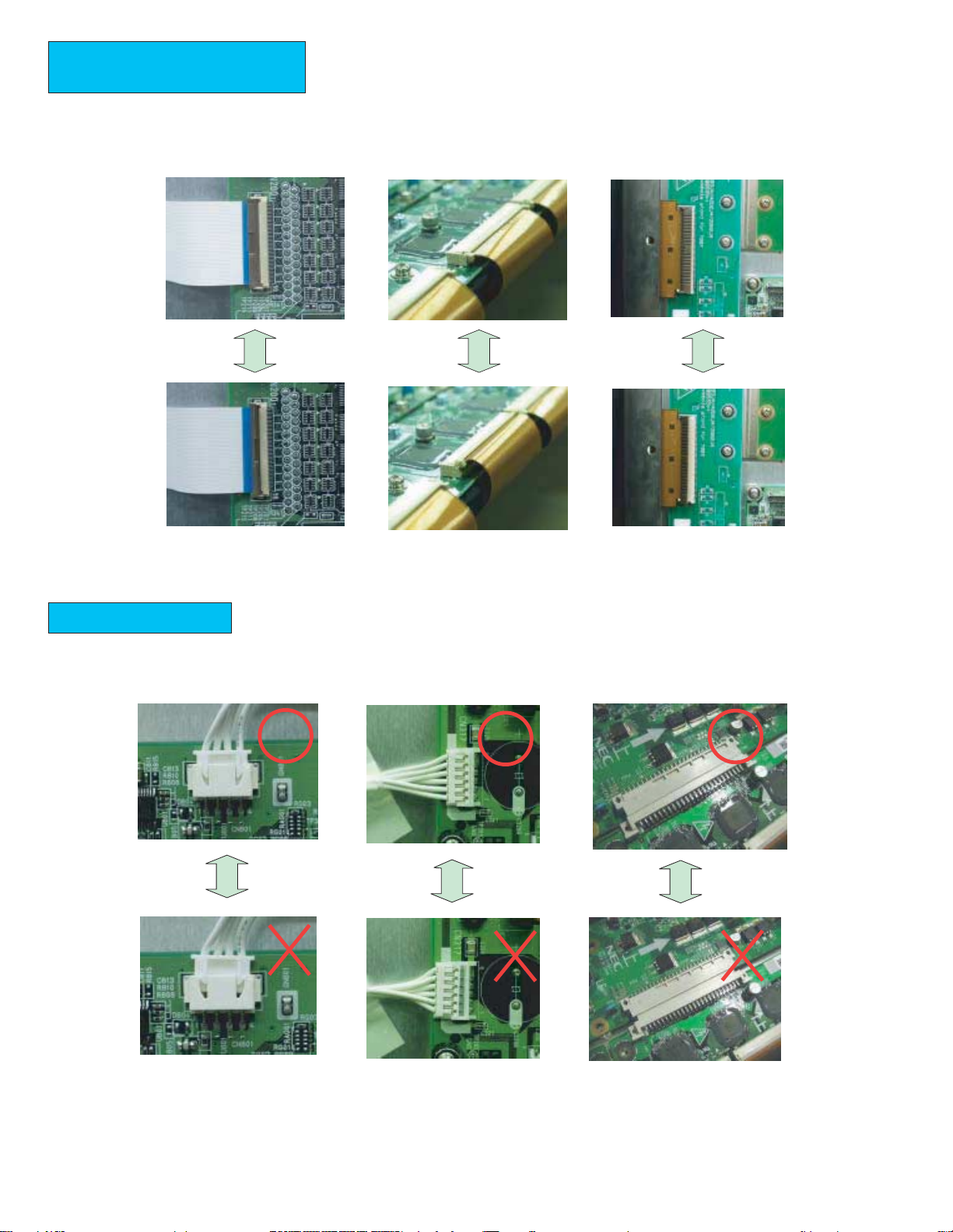
Right Connection (Part 1)
84
Locked
Unlocked
High voltage Board( Photo)
- Digital Board
Scan Relay Board (Photo)
- Panel
Common Relay Board (Photo)
- Panel
Right Connection (Part 2)
Digital Board (Photo)
-High Voltage Board
Locked
Unlocked
High Voltage Board (Photo)
-Data Relay Board
High Voltage Board (Photo)
-Scan Relay Board(Photo)
Page 85
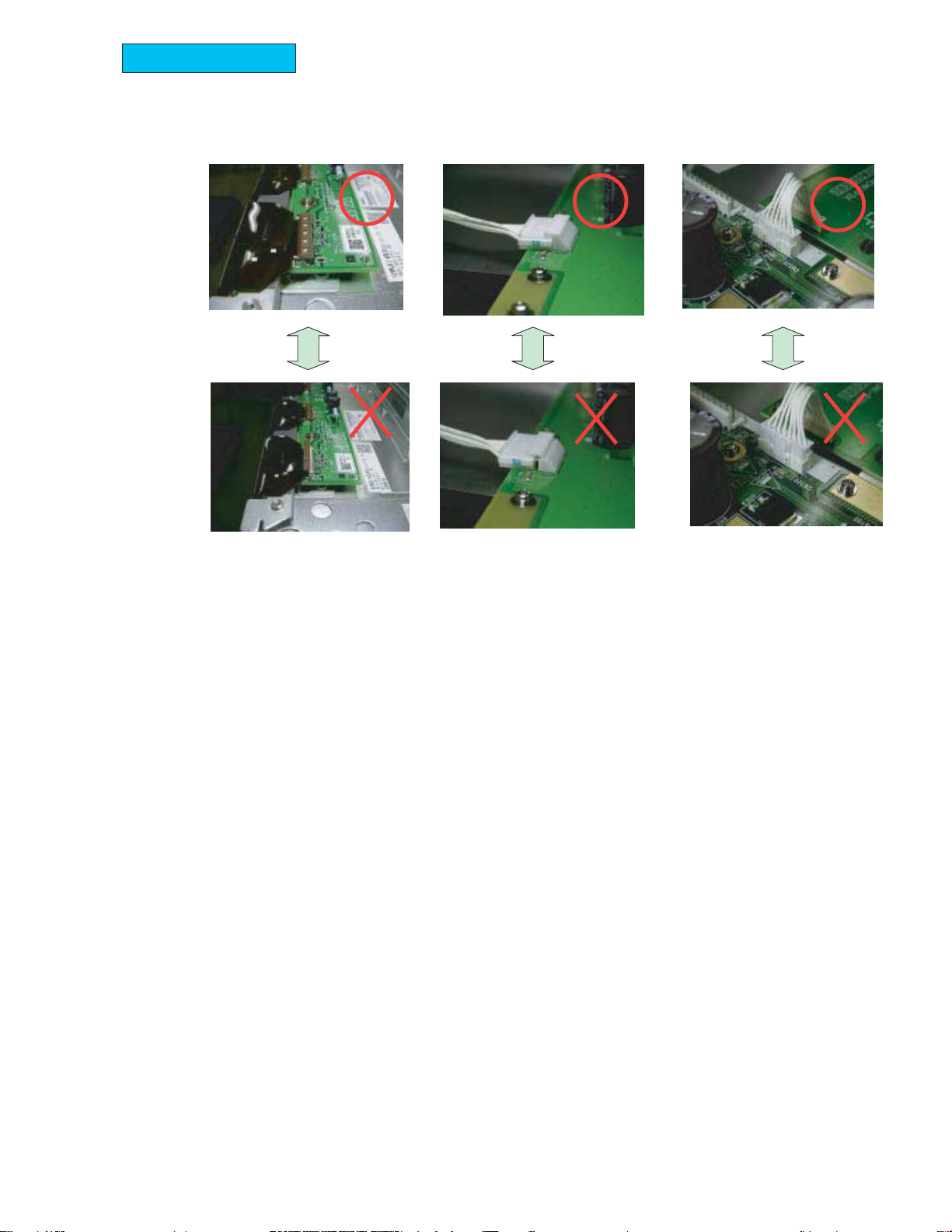
Right Connection (Part 3)
85
Locked
Unlocked
Data Relay Board (Photo)
-Panel
Common Connection Board (Photo)
-Common Relay Board
High Voltage Board (Photo)
-Common Relay Board (Photo)
Page 86
Right Connection (Part 3)
86
Locked
Unlocked
Data Relay Board (Photo)
-Panel
Common Connection Board (Photo)
-Common Relay Board
High Voltage Board (Photo)
-Common Relay Board (Photo)
Page 87
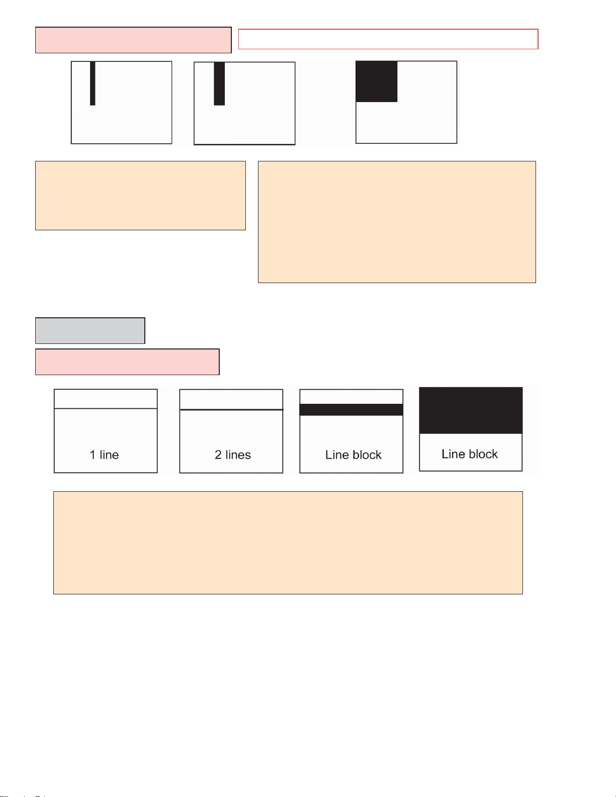
Symptom : Vertical line Block
87
(Note)Typical Symptom are only shown. Another Symptom might appear.
Cause/Countermeasure:
1 Open or contact failure of Data flexible Cable
] Clean, Reconnect or exchange connector.
2 Failure in Data IC
] Exchange PDP.
Horizontal Line
Symptom : Horizontal lines
Cause/Countermeasure:
1 Open or contact failure of connector between Data Relay Board
and Digital Board/High Voltage Board
] Clean, Reconnect or exchange connector.
2 Open or contact failure of multiple Data flexible Cables
] Clean, Reconnect or exchange connector.
3 Failure in Data Relay Board
] Exchange the Data Relay Board.
4 Failure in multiple Data IC
] Exchange PDP.
Cause/Countermeasure:
1 Failure in Scan IC on Scan Relay Board - Exchange Scan Relay Board.
2 Open or contact failure of Scan Flexible Cable (CN01-CN04) at output side of Scan Relay Board (U,D)
] Clean, Reconnect or exchange connector.
3 Contact failure of connector between Scan Board and Scan Relay Board
] Clean, Reconnect or exchange connector.
4 Short between terminals of Scan IC due to screw dust
] Clean around the terminals.
Page 88
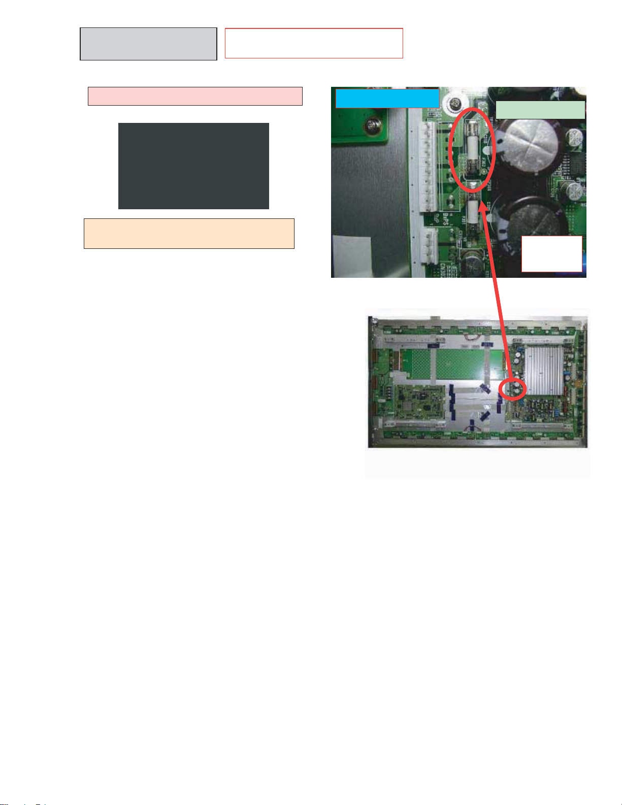
Picture Defect
88
(Note) Typical symptom are only shown.
Another Symptom might appear.
Symptom:No Picture(Priming flash).
Cause/Countermeasure: 1F302 open ]
Exchange High Voltage Board.
High Voltage Board
Glass Fuse (F302)
OK: Short
NG: Open
Page 89
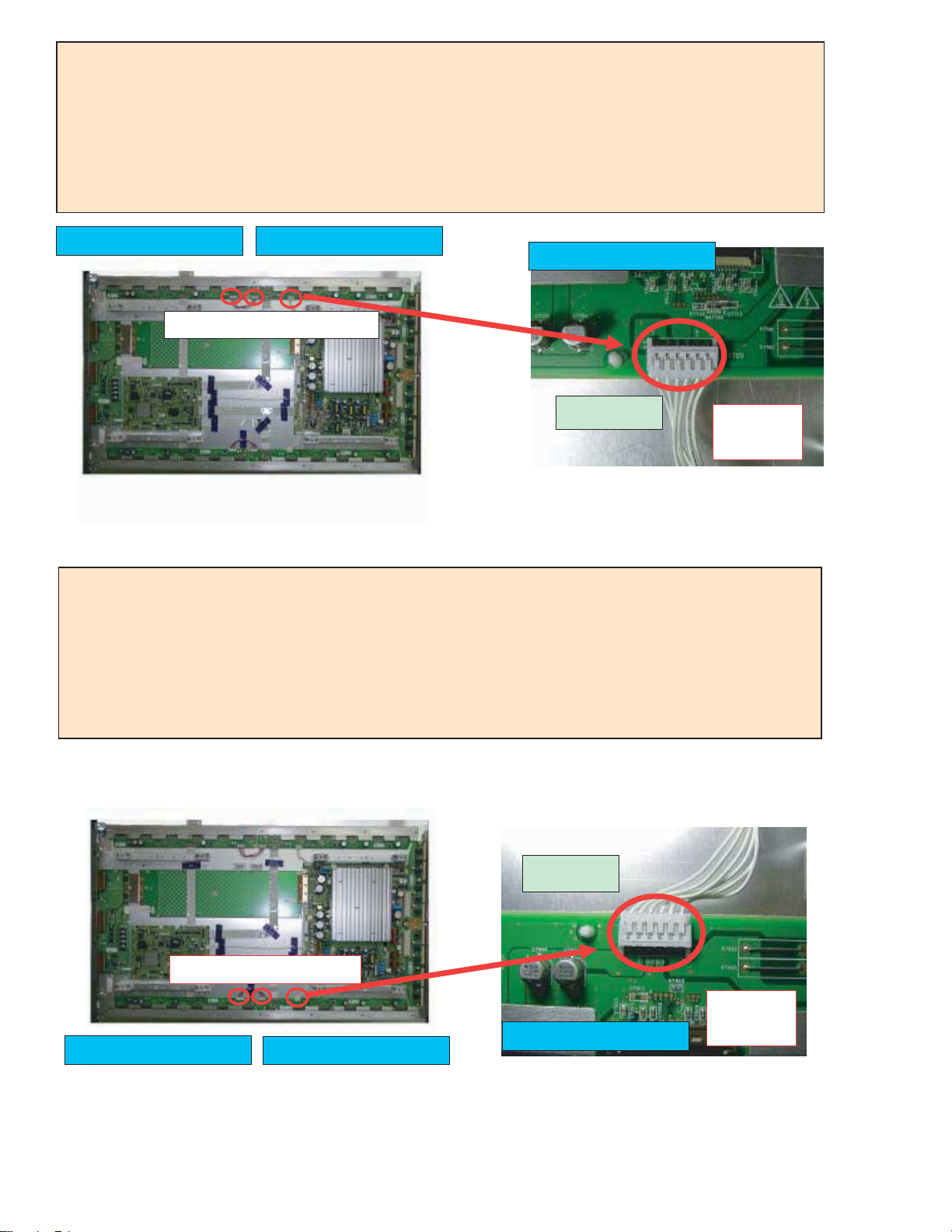
Cause/Countermeasure:
89
2 If the connector CN7709 disconnected from Data Relay Board (RU )is short-circuited between Pin 1 (or 2) and
GND (Pin 3 or 4) ] Data IC is broken ]Exchange PDP.
3 If the connector CN7709 disconnected from Data Relay Board (RU) is short-circuited between Pin 5 (or 6) and
GND (Pin 3 or 4) ] Data Relay Board (LU) or (RU) is failed ]
a) If the connector CN7608 disconnected from Data Relay Board (LU) is short-circuited between Pin 1
and GND (Pin 2 or 6) ]Data Relay Board (LU) is failed ]Exchange Data Relay Board (LU).
b) If the connector CN7708 disconnected from Data Relay Board (RU) is short-circuited between Pin 1
and GND (Pin 2 or 6) ]Data Relay Board (RU) is failed ]Exchange Data Relay Board (RU).
Data Relay Board (LU)
CN7608 CN7708 CN7709
Cause/ Countermeasure :
4 If the connector CN7909 disconnected from Data Relay Board (RD) is short-circuited between Pin 1 (or 2) and
GND (Pin 3 or 4) ] Data IC is broken ] Exchange PDP.
5 If the connector CN7909 disconnected from Data Relay Board (RD) is short-circuited between Pin 5 (or 6) and
GND (Pin 3 or 4) ] Data Relay Board (LD) or (RD) is failed ]
a) If the connector CN7808 disconnected from Data Relay Board (LD) is short-circuited between Pin 8
and GND (Pin 3 or 7) ] Data Relay Board (LD) is failed ] Exchange Data Relay Board (LD).
b) If the connector CN7908 disconnected from Data Relay Board (RD) is short-circuited between Pin 8
and GND (Pin 3 or 7) ] Data Relay Board(RD) is failed ] Exchange Data Relay Board (RD).
Data Relay Board (RU)
Data Relay Board (RU)
CN7709
OK: Open
NG: Short
CN7808 CN7908 CN7909
Data Relay Board (LD)
Data Relay Board (RD)
CN7909
Data Relay Board (RD)
OK: Open
NG: Short
Page 90
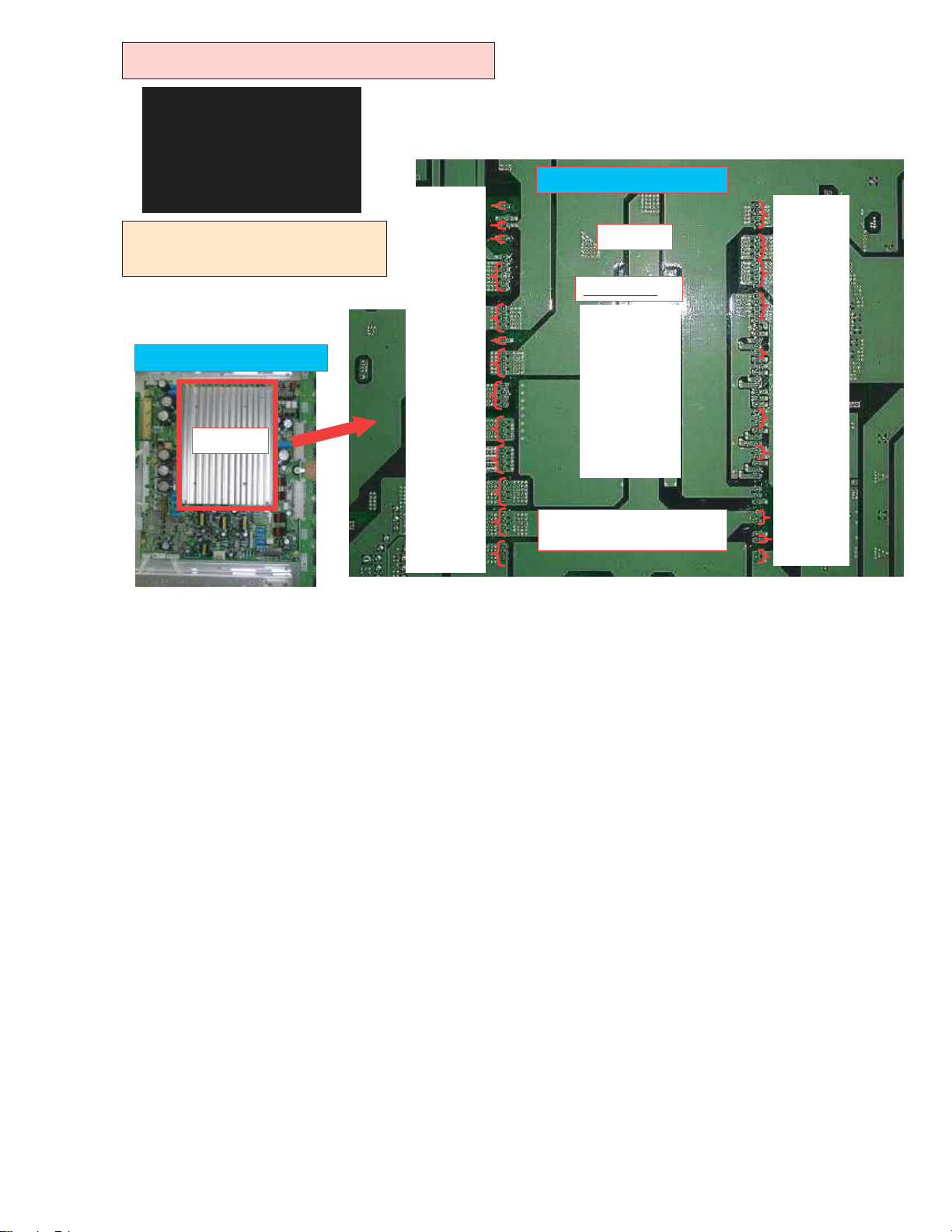
Symptom:No Picture. (Priming doesn’t flash if W-X
90
erminals are short-circuited.)
X (112)
Cause/Countermeasure: No Diode
characteristic ]Exchange High Voltage
Board.
W(109)
V (107)
T (99~103)
S (93~96)
R (91)
High Voltage Board; Surface
Q (86~89)
P (81~84)
PH2401F
O (76~78)
N (71~74)
M (66~69)
L (61~64)
K (57~59)
High Voltage Board; Reverse
PH2401F
Checkpoints
A-D M-L
A-E N-P
B-D O-P
C-D Q-R
E-R R-S
F-N R-T
G-M S-T
H-I T-V
I-J W-X
K-L
OK: Diode characteristic
NG: Other than above
A (1~4)
B (6~9)
C (10~13)
D (15~18)
E (24)
F (33~35)
G (39~40)
H (49~50)
I (53)
J (55~56)
Page 91
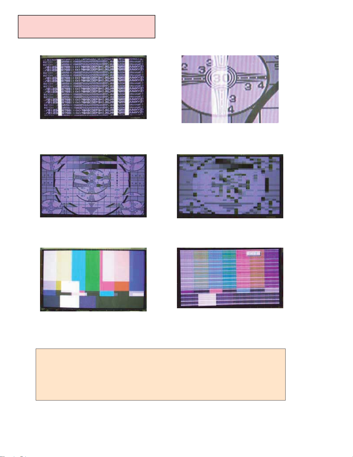
Symptom:Abnormalities in a picture
91
One or more vertical bands,
Multiple vertical lines
Out of synchronization or
duplication
Tr ansparent vertical band
Mosaic
Rectangular color shear,color discrepancy,
shear in display
Cause/Countermeasure : 1 Contact failure of connector adjacent to Digital Board or short circuit due to
conductive obstacle
] Clean or Reconnect
2 Failure in circuit on Digital Board
] Failure in Digital Board
A number of lateral lines,
Regular noise
Page 92
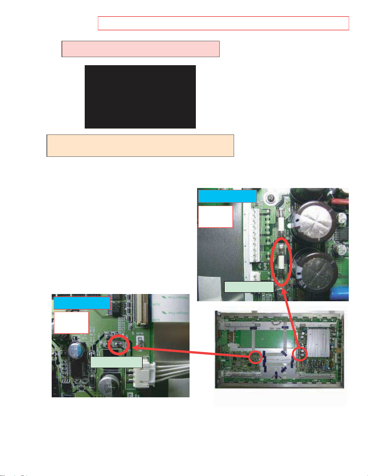
Power off
92
Symptom: No Picture(Priming doesn’t flash) ] Power off
(Note) Typical Symptom are only shown. Another Symptom might appear.
Cause/Countermeasure: 1 F301 open ] Exchange High Voltage Board.
2 FU801 open ] Exchange Digital Board.
High Voltage Board
OK: Short
NG: Open
Digital Board
Glass Fuse (F301)
OK: Short
NG: Open
Chip Fuse (FU801)
Page 93
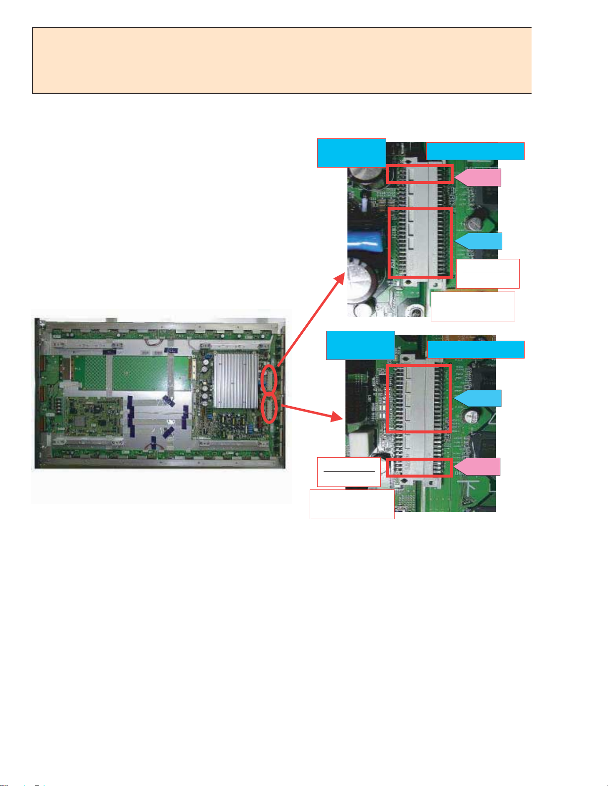
Cause/Countermeasure : If short-circuited, disconnect connector between High Voltage Board and Scan Relay Board and,
93
4 Short between NEGA-POSI on High Voltage Board ]Exchange High Voltage Board.
5 Short between NEGA-POSI on Scan Relay Board (U) ]Exchange Scan Relay Board (U).
6 Short between NEGA-POSI on Scan Relay Board (D) ]Exchange Scan Relay Board (D).
High Voltage
Board
High Voltage
Board
Scan Relay Board (U)
NEGA
POSI
Checkpoint
NEGA-POSI
OK: More than kΩ
NG: Short
Scan Relay Board (D)
POSI
Checkpoint
NEGA-POSI
OK: More than kΩ
NG: Short
NEGA
Page 94
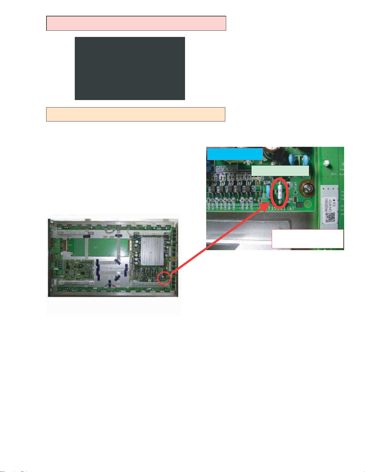
Symptom: No Picture ] Power off(Priming flash)
94
Cause/Countermeasure: R91 open ] Exchange High Voltage Board.
High Voltage Board
Fuse Resistor (R91)
R91 OK: About 2.2 Ω(1W)
NG: Open
Page 95
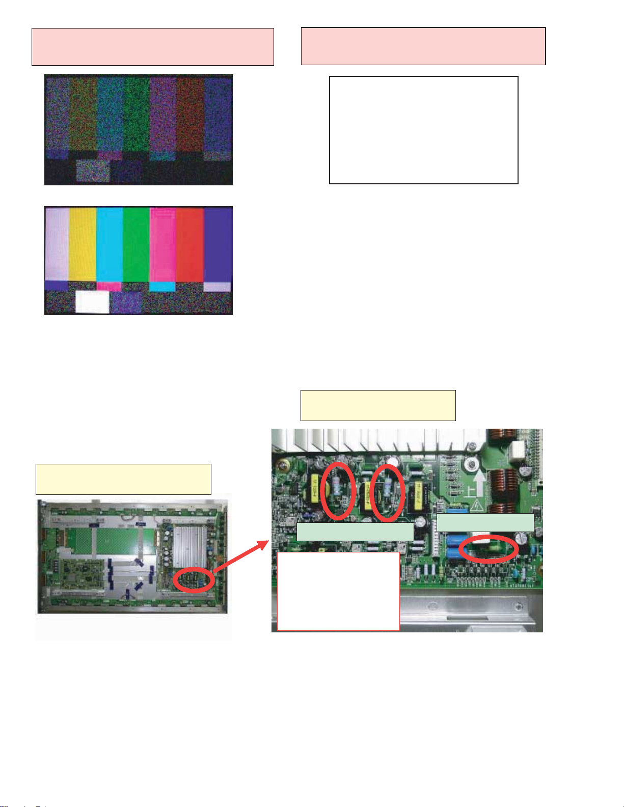
Symptom: Failure in Writing
95
] Power off
Dark and rough picture
Many light spots on dark portion
Symptom: White pattern even in no
signal ] Power off
Cause/Countermeasure: R43,R61 open
] Exchange High Voltage Board.
Cause/Countermeasure:R150 open
] ExchangeHigh Voltage Board.
Fuse Resistor (R150)
Fuse Resistor (R43),(R61)
R43 OK: About 3.3 Ω(2W)
NG: Open
R61 OK: About 4.7 Ω(2W)
NG: Open
R150 OK: About 4.7 Ω(2W)
NG: Open
Page 96
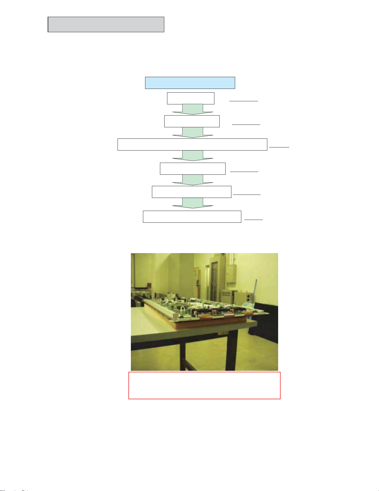
METHOD OF DISASSEMBLY
96
Follow the procedure below for diagnosis.
Disassembly
Prepare tools.
Prepare product.
Disconnect connectors and cables on failed Board.
Detach failed Board.
Put on good Board.
Connect connectors and cables.
Right photo
Right photo
Page 128
Page129-130
Page129
Page 128
(Caution) Put cushion under failed PDP to cover
general surface of glass before laying it’s screen
down.
Page 97
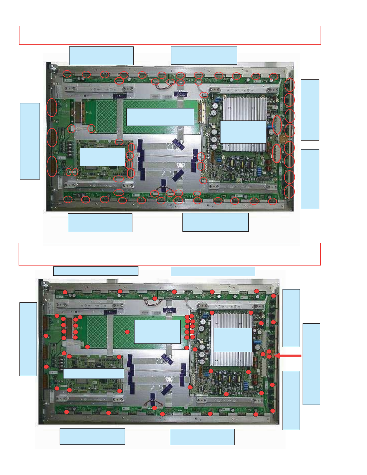
Detach connectors and cables on failed Board.
97
(Caution) Be careful of handling cables and connectors to avoid Failure. Be sure to take off Heat Sink before detach Data
Relay Board. See Page 30 for the procedure.
Data Relay Board (LU)
8 connectors
5 connectors
Common Connection Board
Digital Board
7 connectors
Data Relay Board (LD)
8 connectors
Data Relay Board (RU)
Common Relay Board
1 connector
9 connectors
High Voltage
Board
6 connectors
Data Relay Board (RD)
9 connectors
5 connectors
Scan Relay Board (U)
5 connectors
Scan Relay Board (D)
Loosen screws of failed Board and put on good Board.
(Caution) Be careful not to leave screwdriver, screw or screw dust. Be sure to take off Heat Sink before detach Data Relay
Board. See the next page for the procedure.
Data Relay Board (LU); 3 screws
9 screws
Common Connection Board
Digital Board 4 screws
Common Relay
Board15
screws
Data Relay Board (RU); 3 screws
High Voltage
Board15
screws
2 screws
Scan Relay Board (U)
2 screws
2 screws
Scan Relay Connection Board
Data Relay Board (LD)
3 screws
Scan Relay Board (D)
Data Relay Board (RD)
3 screws
Page 98
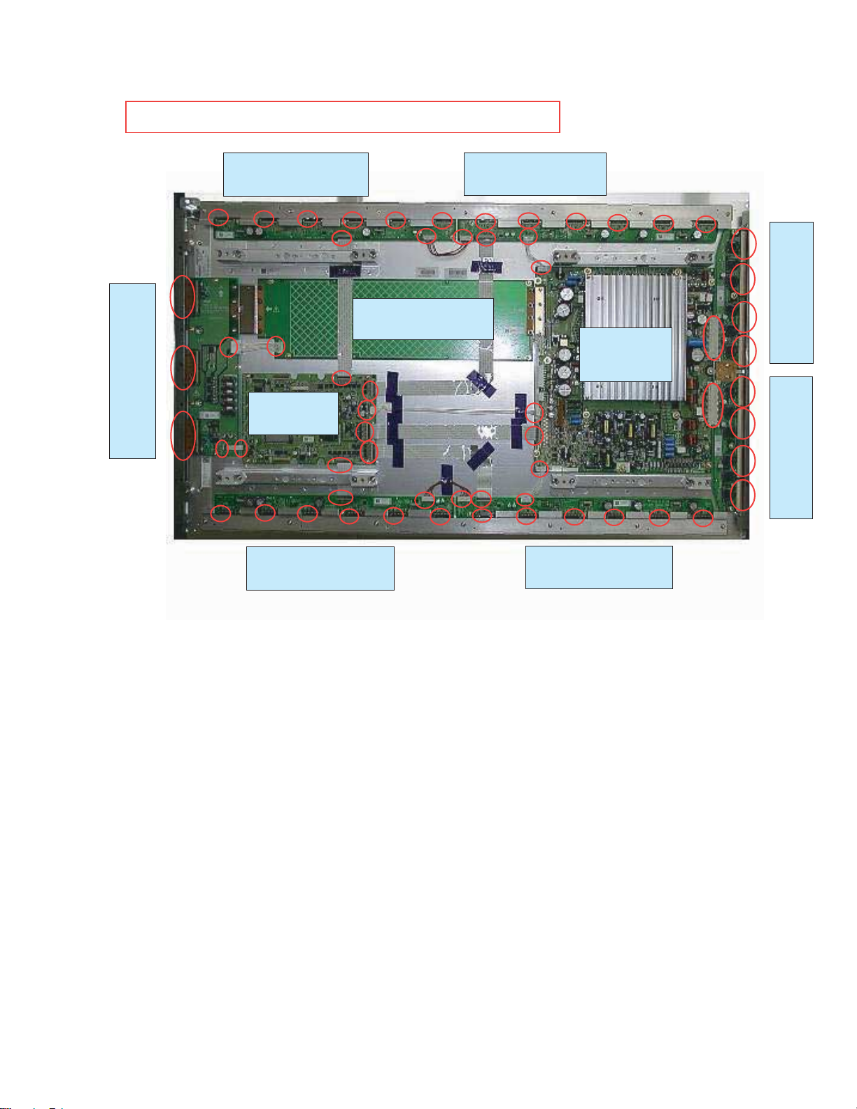
Put on connectors and cables of good Board.
98
(Caution) Be sure to put on Heat Sink after assembling Data Relay Board.
Data Relay Board (LU)
8 connectors
5 connectors
Common Connection Board
Digital Board
7 connectors
Data Relay Board (LD)
8 connectors
Data Relay Board (RU)
Common Relay Board
1 connector
9 connectors
Data Relay Board (RD)
9 connectors
High Voltage
Board
6 connectors
5 connectors
Scan Relay Board (U)
5 connectors
Scan Relay Board (D)
Page 99
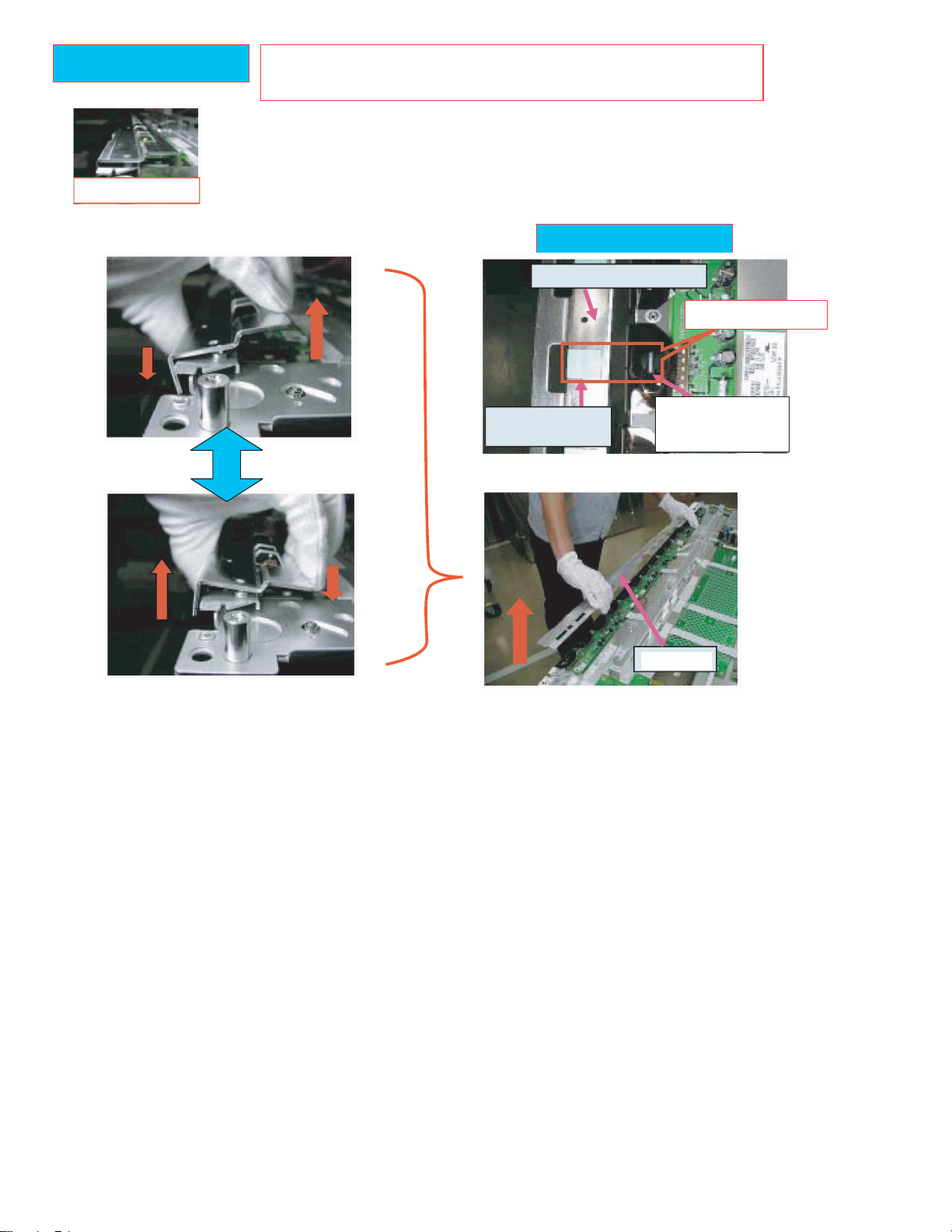
How to detach Heat Sink
99
Before detaching
(Caution) Stress on detaching easily breaks flex cable because Data TCP is
sticking with Heat Sink (heat-conductive silicone sheet).(See Photo4)
1. Slowly swing Heat Sink back and forth.(1,2)
2. Gently lift Heat Sink up from Data TCP.(1,2)
3. Repeat1 and 2 until Heat Sink is taken off.(3)
Heat Sink and Data TCP
1
2
4
Heat-conductive
silicone sheet
Reverse of Heat Sink
3
Be careful of sticking.
Data TCP mounted
on Flexible cable
Heat Sink
Page 100
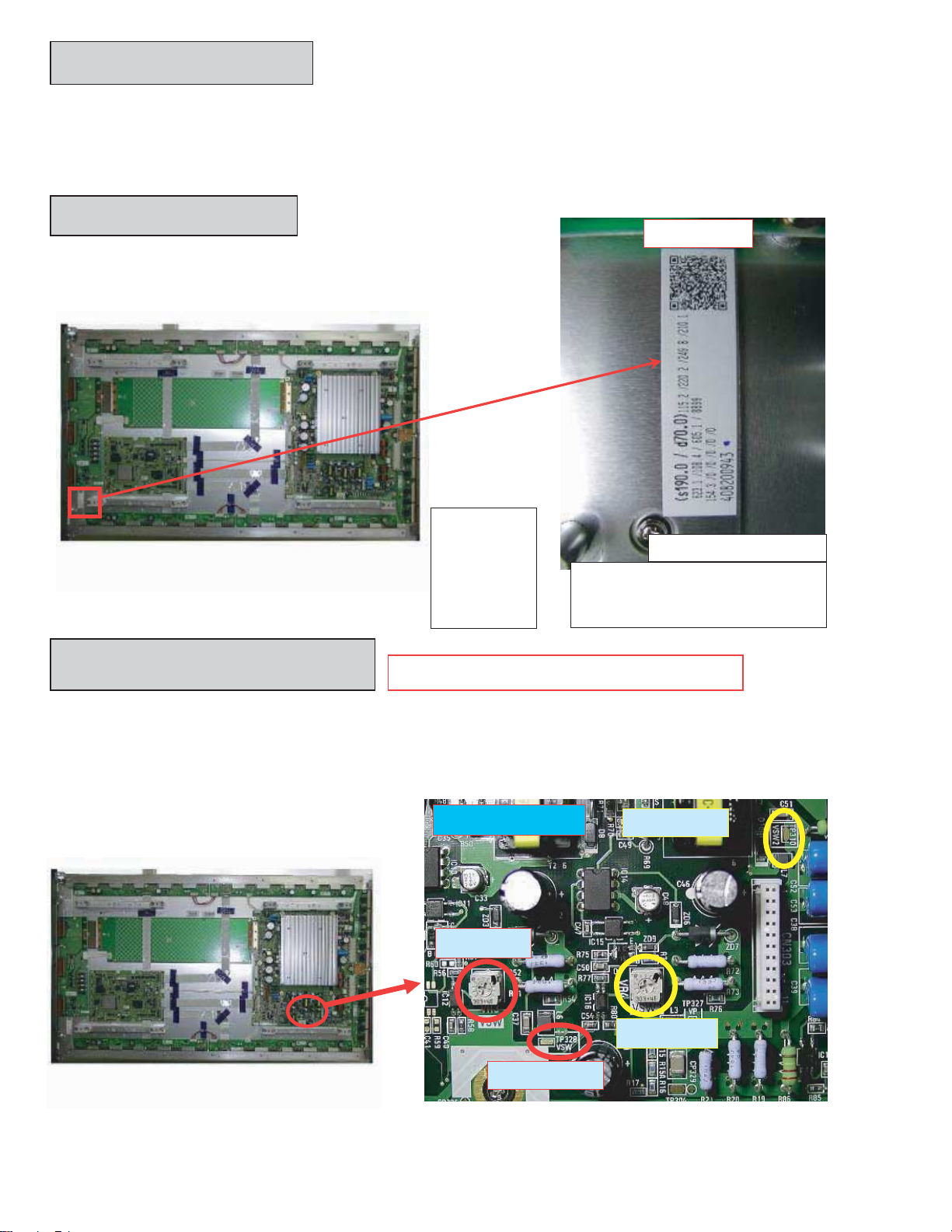
(1) Adjustments
100
Follow the procedure below.
1-1)Conduct “(3)Adjustment of Vsw1 & Vsw2”and“(4)Adjustment of Vbw& Vp”, when High Voltage Board is replaced.
1-2) There is no need of adjustment if Board other than High Voltage Board.
(2) Voltage Label Check
Voltage Label
Be sure to confirm voltages on Voltage label before conducting adjustment.
Example
Vbw : 115.2
Vsw1 : 220.2
VP : 249.8
Vsw2 : 210.1
(3) Adjustment of Vsw1 & Vsw2
Vsw1 : Adjust VR3 so that the voltage between Test Pad (TP328) and GND becomes
“Rated Voltage on Label ± 0.5V”.
Vsw2 : Adjust VR4 so that the voltage between Test Pad (TP310) and GND becomes
“Rated Voltage on Label ± 0.5V”.
(Caution) Use the nearest chassis for grounding.
High Voltage Board
VR3 Vsw1
(s190.0/d70.0)115.2/220.2/249.8/210.1
*************************************
408200943
Vbw Vsw1
TP310 Vsw2
Vp
Vsw2
VR4 Vsw2
TP328 Vsw1
 Loading...