

Page 1
PIONEER ELECTRONIC CORPORATION 4-1, Meguro 1-Chome, Meguro-ku, Tokyo 153-8654, Japan
PIONEER ELECTRONICS SERVICE INC. P.O.Box 1760, Long Beach, CA 90801-1760 U.S.A.
PIONEER ELECTRONIC [EUROPE] N.V. Haven 1087 Keetberglaan 1, 9120 Melsele, Belgium
PIONEER ELECTRONICS ASIACENTRE PTE.LTD. 501 Orchard Road, #10-00, Wheelock Place, Singapore 238880
C PIONEER ELECTRONIC CORPORATION 1998
K-ZEU MAY 1998 Printed in Japan
ORDER NO.
CRT2197
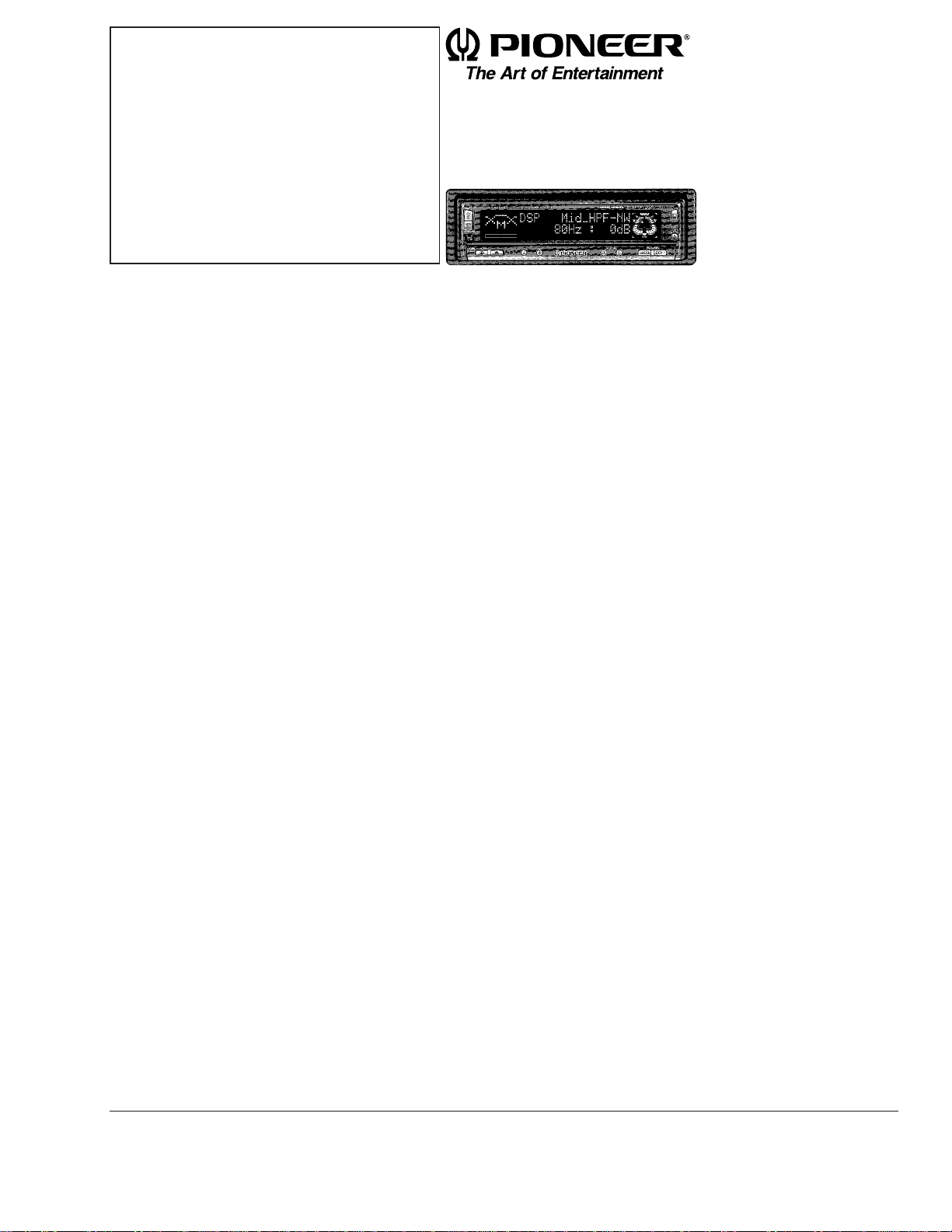
MULTI-CD/MD/DAB CONTROL DSP HIGH POWER CASSETTE PLAYER WITH RDS TUNER
Se
r
vic
e
M
a
nu
a
l
KEH-P9700R EW
NOTE:
- See the separate manual CX-631(CRT1640) for the cassette mechanism description.
- The cassette mechanism assy employed in this model is one of 2L series
- Dolby noise reduction manufactured under license from Dolby Laboratories Licensing Corporation.
"Dolby" and the double-D symbol are trademarks of Dolby Laboratories Licensing Corporation.
- This service manual does not describe the CD test mode.
For the operations in the CD test mode, refer to the CD player's Service Manual.
KEH-P9750 ES
CONTENTS
1. SAFETY INFORMATION............................................2
2. EXPLODED VIEWS AND PARTS LIST......................2
3. SCHEMATIC DIAGRAM...........................................10
4. PCB CONNECTION DIAGRAM................................31
5. ELECTRICAL PARTS LIST........................................45
6. ADJUSTMENT.........................................................58
7. GENERAL INFORMATION.......................................60
7.1PARTS .................................................................60
7.1.1 IC...............................................................60
7.1.2 DISPLAY...................................................70
7.2DIAGNOSIS........................................................71
7.2.1 DISASSEMBLY.........................................71
7.3EXPLANATION ...................................................72
7.3.1 BLOCK DIAGRAM....................................72
8. OPERATIONS AND SPECIFICATIONS....................74
KEH-P9750/ES
MULTI-CD CONTROL DSP HIGH POWER CASSETTE PLAYER WITH FM/AM TUNER
Page 2
2
KEH-P9700R,P9750
1. SAFETY INFORMATION
This service manual is intended for qualified service technicians; it is not meant for the casual do-it-yourselfer.
Qualified technicians have the necessary test equipment and tools, and have been trained to properly and safely repair
complex products such as those covered by this manual.
Improperly performed repairs can adversely affect the safety and reliability of the product and may void the warranty.
If you are not qualified to perform the repair of this product properly and safely, you should mot risk trying to do so
and refer the repair to a qualified service technician.
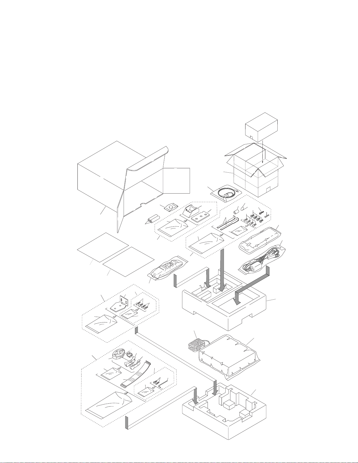
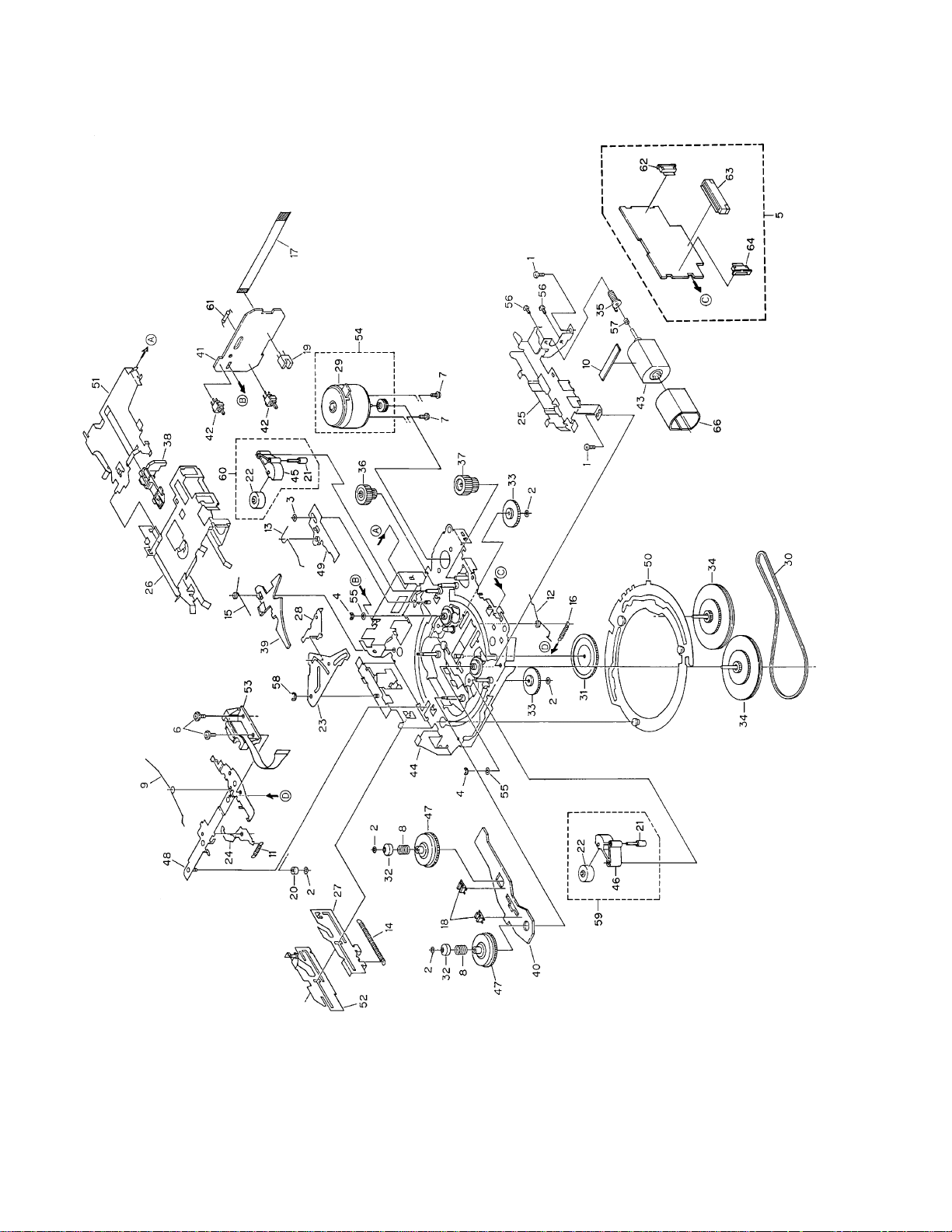
2. EXPLODED VIEWS AND PARTS LIST
2.1 PACKING
38
39
35
37
44
5
14
4
34
47
10
7
9
23
11
12
8
13
45
46
21
39
16
17
18
19
3
20
15
22
1
24
2
42
41
6
26
27
28
25
29
30
32
31
33
Page 3

3
KEH-P9700R,P9750
* 1 Cover CEG1088
2 Protector(EW) CHP2090
Protector(ES) CHP2033
3 Bracket Assy CEA2346
4 Protector(EW) CHP2089
Protector(ES) CHP2032
5 Case Assy CXA7194
6 Remote Control Assy
(EW) CXB2636
7 Battery CEX1006
8 Battery(EW) CEX1030
9 Microphone Assy CPM1022
10 Base Assy CEA2426
* 11 Base CNS5031
* 12 Seat CZA3371
13 Polyethylene Bag CZE3188
14 Cord Assy(EW) CDE5668
Cord Assy(ES) CDE5669
15 Screw Assy CZE3198
* 16 Polyethylene Bag CEG-127
17 Screw BNC40P120FZK
18 Screw BPZ30P100FZK
* 19 Polyethylene Bag CZE3201
20 Bracket CZN6467
* 21 Accessory Assy(EW) CEA2429
22 Air Cap CEG1080
23 Carton(EW) CHG3535
Carton(ES) CHG3505
24 Contain Box(EW) CHL3535
Contain Box(ES) CHL3505
25 Screw Assy(EW) CZE3169
* 26 Polyethylene Bag(EW) CEG-127
27 Hexagon Wrench(EW) CZE3176
28 Screw(EW) RMZ30H060FBK
29 Belt(EW) CZN6416
30 Remote Control Assy
(EW) CZX3218
31 Cover(EW) CZN6410
32 Holder Assy(EW) CZX3172
33 Holder Assy(EW) CZX3173
34 Remote Control Assy
(EW) CXB2659
Remote Control Assy
(ES) CXB2656
* 35 Polyethylene Bag E36-615
* Polyethylene Bag CEG-158
36 Bush CNV1917
37 Handle CNC5395
38 Spring CBH-865
39 Screw CBA1120
40 Screw CBA1002
41-1 Polyethylene Bag CEG1116
41-2 Owner's Manual(EW) CRD2636
Owner's Manual(ES) CRD2642
41-3 Owner's Manual(EW) CRD2637
Owner's Manual(ES) CRD2643
41-4 Owner's Manual(EW) CRD2638
41-5 Installation Manual(ES) CRD2644
41-6 Installation Manual(ES) CRD2645
42-1 Polyethylene Bag(EW) CEG1116
42-2 Installation Manual(EW) CRD2639
42-3 Installation Manual(EW) CRD2640
42-4 Installation Manual(EW) CRD2641
42-5 Passport(EW) CRY1013
* 42-6 Warranty Card(EW) CRY1087
* 42-7 Card(EW) CRD1183
* 42-7 Card(ES) CRD1186
* 42-8 Card(EW) CRD1184
* 42-9 Card(EW) CRD1185
* 43 Screw Assy(ES) CEA2434
* 44 Polyethylene Bag(ES) CEG-127
45 Screw(ES) BMZ50P060FMC
46 Screw(ES) CMZ50P060FMC
* 47 Accessory Assy(ES) CEA2431
NOTE:
- Parts marked by “*” are generally unavailable because they are not in our Master Spare Parts List.
- Screws adjacent to
∇ mark on the product are used for disassembly.
- Parts List
Mark No. Description Part No. Mark No. Description Part No.
- Owner's Manual, Installation Manual
Model Part No. Language
KEH-P9700R/EW CRD2636,CRD2639 English,Spanish
CRD2637,CRD2640 German,French
CRD2638,CRD2641 Italian,Dutch
KEH-P9750/ES CRD2642,CRD2644 English,Spanish
CRD2643,CRD2645 Portuguese(B),Arabic
Page 4
A
A
23
64(2/2)
72
157
65
23
21
30
33
2
63
62
14
15
20
56
57
133
160
37
37
23
58
53
41
32
34
31
22
21
24
24
78
126
29
50
49
46
61
51
44
43
45
36
110
81
101
92
24
90
107 90
16
158
82
159
82
25
94
83
24
114
93
115
1
13
2
155
35
35
162
12
26
129
28
127
127
130
128
132
131
1
1
1
95
125
156
106
79
121
124
123
99
88
80
80
80
80
96
113
84
116
88
81
101
90
101
108
102
101
90
102
118
87
10
90
117
98 91 119
98
91
90
120
105
85
104
85
105
86
109
111
8989111
100
86
103
9
11
8
122
19
54
39
39
52
48
40
77
76
75
73
64(1/2)
55
42
66
69
71
70
68
67
47
161
20
59
38
60
97
17
163
27
18
18
18
4
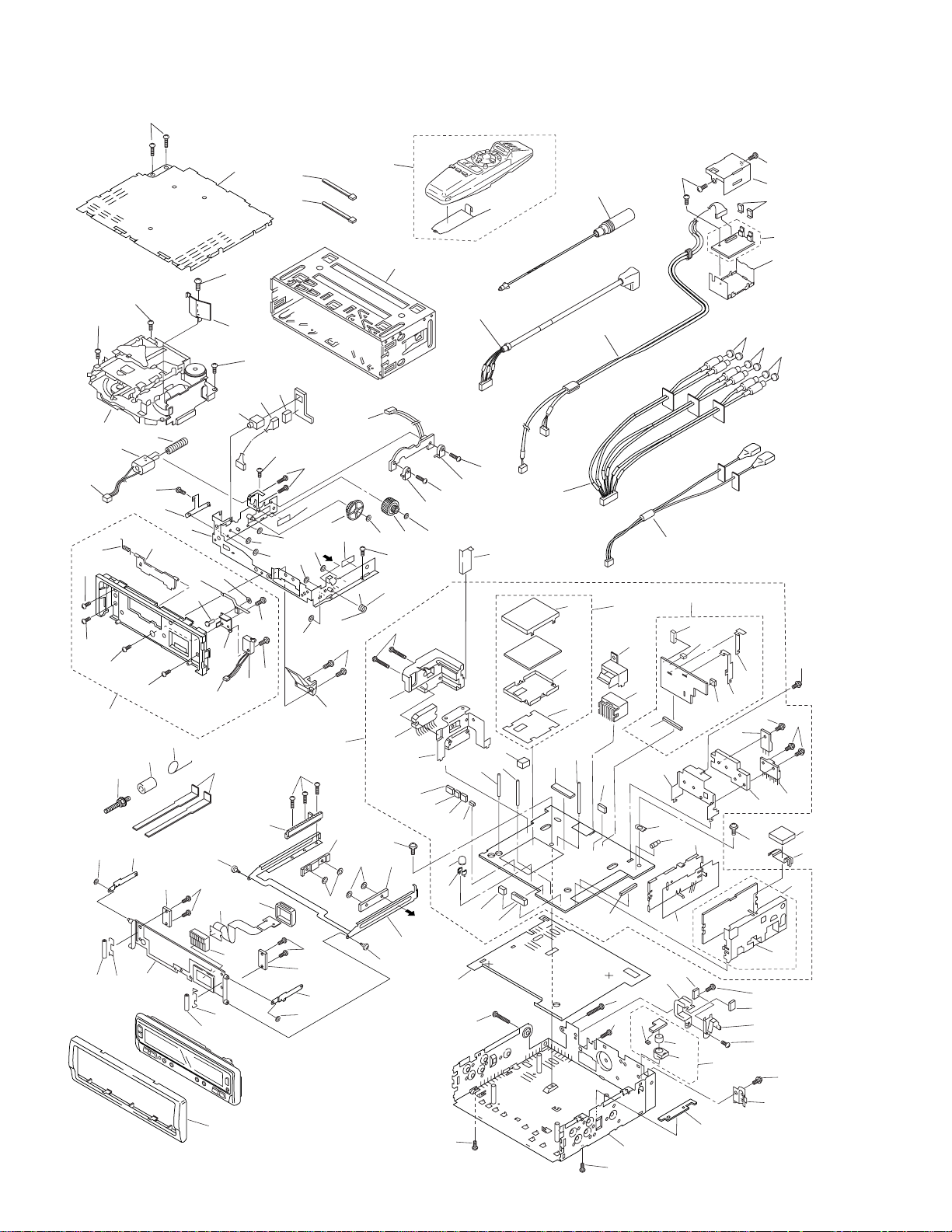
KEH-P9700R,P9750
2.2 EXTERIOR
Page 5
5
KEH-P9700R,P9750
164
167
165
165
167
166
3
6
5
7
6
4
154
142
137
139
141
144
140
138
136
148
146
150
112
151
149
145
134
143
152
147
153
135
135
135
Page 6

6
KEH-P9700R,P9750
1 Screw BSZ26P050FMC
2 Screw BSZ30P055FMC
3 Cord Assy(EW) CDE5668
4 Fuse 10A(EW) CEK1136
5 Cap(EW) CKX-003
6 Cap(EW) CNS1472
7 Resistor(EW) RS1/2PMF102J
8 Screw CBA1002
9 Spring CBH-865
10 Handle CNC5395
11 Bush CNV1917
12 Holder CNC6798
13 Shield CNC7609
14 Earth Terminal(EW) CNC8019
Earth Terminal(ES) CNC7358
15 Spacer CNM4913
16 Spacer CNM6052
17 Panel(EW) CNS4553
Panel(ES) CNS4320
18 Cap CNV2680
19 IC(IC251) TDA7386
20 Screw ASZ26P055FUC
21 Screw BMZ30P180FMC
22 Screw BSZ26P080FMC
23 Screw BSZ30P055FMC
24 Screw CBA1447
25 Cord Assy CDE5588
26 Cord Assy CDE5663
27 Cord Assy CDE5664
28 Antenna Cord CDH1251
29 Holder CNC4963
30 Holder CNC7566
31 Holder CNC7753
32 Insulator CNM5628
33 Cushion CNM5811
34 Cushion CNM5812
* 35 Lock Tie CNV-754
36 Tuner Amp Unit(EW) CWM5781
Tuner Amp Unit(ES) CWM5782
37 Screw ASZ26P100FMC
38 Screw BMZ26P200FMC
39 Clamper CEF1006
40 Clamper CEF1009
41 Terminal(CN402) CKF1059
42 Plug(CN251) CKM1278
43 Plug(CN951) CKS-783
44 Plug(CN952) CKS-784
45 Plug(CN171) CKS-786
46 Plug(CN803) CKS1222
47 Plug(CN804) CKS1225
48 Plug(CN201) CKS1246
49 Connector(CN801) CKS1564
50 Connector(CN751) CKS1730
51 Connector(CN953) CKS3124
52 Connector(CN101) CKS3781
53 Antenna Jack(CN401) CKX1010
54 Holder CNC7554
55 Holder CNC8008
56 Holder CNC8016
57 Heat Sink CNC8020
58 Holder CNC8021
59 Insulator CNM4684
60 Heat Sink CNR1468
61 Holder CNV1906
62 FM/AM Tuner Unit(EW) CWE1416
FM/AM Tuner Unit(ES) CWE1485
63 Holder CNC6555
64 ASL Unit CWM5783
65 Connector(CN302) CDE5667
* 66 Plug(CN701) CKS1058
67 Plug(CN703) CKS1624
68 Connector(CN301) CKS2191
69 Connector(CN601) CKS3582
70 Holder CNC6676
71 Holder CNC8017
72 Holder CNV5375
73 DSP Unit(EW) CWX2237
DSP Unit(ES) CWX2238
74 Connector(CN3001) CKS3782
75 Case CNC8014
76 Case CNC8015
77 Insulator CNM5626
78 Chassis Unit(EW) CXB2231
Chassis Unit(ES) CXB2296
79 Screw BMZ20P030FMC
80 Screw BMZ20P030FZK
81 Screw BPZ20P060FMC
82 Screw CBA1060
83 Screw CBA1061
84 Screw CBA1070
85 Screw CBA1082
86 Screw CBA1430
87 Screw CBA1454
88 Washer CBF-046
89 Washer CBF1038
90 Washer CBF1039
91 Spring CBH2063
92 Spring CBH2086
93 Cord CDE5587
94 Cord CDE5712
- Parts List
Mark No. Description Part No. Mark No. Description Part No.
Page 7

7
KEH-P9700R,P9750
95 Cord CDE5713
96 Connector CDE5738
97 Socket CKS2497
98 Roller CLA3458
99 Arm CNC1280
100 Frame CNC7548
101 Spacer CNM5808
102 Spacer CNM5988
103 PCB CNP5068
104 Cover CNS4841
105 Holder CNV2141
106 Gear CNV5271
107 Gear Unit CNV5272
108 Gear CNV5273
109 Rack CNV5274
110 Lighting Conductor CNV5287
111 Guide CNV5356
112 EL(EL1901) CEL1580
113 Switch CSN-088
114 Jack(CN4602) CKN1015
115 Plug(CN4601) CKS-786
116 Holder Unit CXA8599
117 Arm Unit CXB2215
118 Frame Unit CXB2216
119 Holder Unit CXB2217
120 Arm Unit CXB2218
121 Bracket Unit CXB2598
122 Panel Unit CXB2678
Panel Unit CXB2679
123 Door CAT1963
124 Spring CBH2184
125 Motor(M951) CXM1085
126 Guide Unit CXB3234
127 Screw BSZ26P050FMC
128 Clip MBK9001
129 Cord MDE9019
130 Holder MNC9008
131 Holder MNC9009
132 Inverter Unit MWM9026
133 IC(IC901) PA2024A
134 Detach Grille Assy(EW) CXB2610
Detach Grille Assy(ES) CXB2611
135 Screw BPZ20P080FZK
136 Button(+,-) CAC5486
137 Button(EJECT) CAC5488
138 Button(EW)(S/A,CLOCK) CAC5491
Button(ES)(S/A,CLOCK) CAC5490
139 Button(TRACK) CAC5494
140 Button(P,D) CAC5498
141 Button CAC5499
142 Button(S) CAC5504
143 Spacer CNM5910
144 Spacer CNM6021
145 Keyboard Unit(EW) CWM5688
Keyboard Unit(ES) CWM5689
* 146 LCD(LCD1901) CAW1471
147 Plug(CN1901) CKS2496
148 Holder CNC7547
149 Spacer CNM5622
150 Spacer CNM5623
151 Spacer CNM5894
* 152 PCB CNP5063
153 Cover Unit(EW) CXB2208
Cover Unit(ES) CXB2207
154 Grille Unit(EW) CXB2223
Grille Unit(ES) CXB2224
155 Case Unit CXB3114
156 Cassette Mechanism Module EXK3375
157 Microphone(MIC301) CPM1011
158 Switch(S951) CSN1012
159 Switch(S952) CSN1022
160 IC(IC902) NJM7805FA
161 Lamp(IL801) CEL1359
162
Remote Control Assy(EW) CXB2659
Remote Control Assy(ES) CXB2656
163 Battery Cover CNS5032
164 Cord Assy(ES) CDE5669
165 Cap(ES) CNS1472
166 Fuse 10A(ES) CEK1136
167 Resistor(ES) RS1/2PMF102J
Mark No. Description Part No.
Mark No. Description Part No.
Page 8
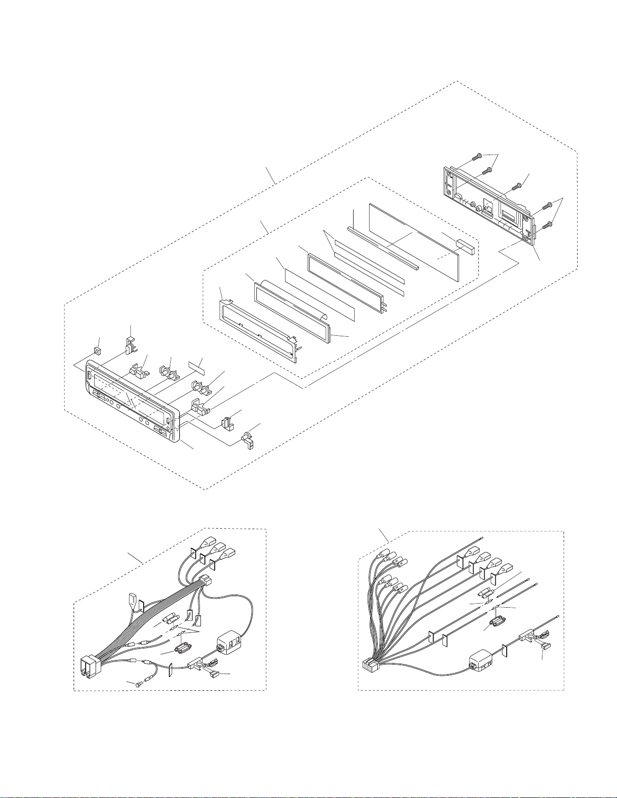
8
KEH-P9700R,P9750
2.3 CASSETTE MECHANISM MODULE
Page 9

9
KEH-P9700R,P9750
- CASSETTE MECHANISM MODULE
- PARTS LIST
Mark No. Description Part No.
Mark No. Description Part No.
1 Screw BSZ20P040FMC
2 Washer CBF1037
3 Washer CBF1038
4 Washer CBG1003
5 Deck Unit EWM1020
6 Screw EBA1028
7 Screw EBA1037
8 Spring EBH1531
9 Spring EBH1575
10 Cushion EWM1034
11 Spring EBH1515
12 Spring EBH1587
13 Spring EBH1517
14 Spring EBH1518
15 Spring EBH1519
16 Spring EBH1537
17 Cord EDD1015
18 Photo-interrupter
(EGN2,3) EGN1006
19 Photo-interrupter(EGN1) EGN1005
20 Roller ENR1031
21 Shaft ELA1373
22 Pinch Roller ENV1518
23 Arm ENC1489
24 Arm ENC1397
25 Guide ENC1398
26 Holder ENC1417
27 Lever ENC1448
28 Arm ENC1488
29 Motor EXM1027
30 Belt ENT1027
31 Gear ENV1347
32 Pulley ENV1503
33 Gear ENV1350
34 Flywheel ENV1410
35 Worm Gear ENV1439
36 Worm Wheel ENV1440
37 Gear ENR1028
38 Lever ENV1442
39 Arm ENV1525
40 Gathering P.C.Board ENX1037
41 P.C.Board ENP1152
42 Switch(S1,S2) ESG1004
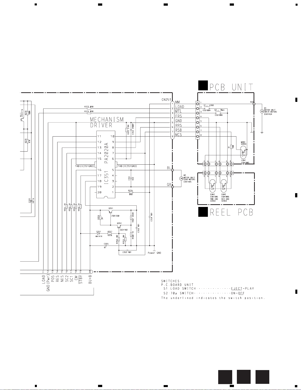
43 Motor Unit(M2) EXA1485
44 Chassis Unit EXA1511
45 Pinch Holder ENV1485
46 Pinch Holder ENV1486
47 Reel Unit EXA1543
48 Head Base Unit EXA1457
49 Lever Unit EXA1438
50 Gear Unit EXA1436
51 Frame Unit EXA1458
52 Lever Unit EXA1439
53 Head Assy(HD1) EXA1527
54 Motor Unit(M1) EXA1490
55 Washer HBF-179
56 Screw BMZ20P022FMC
57 Spring EBH1545
58 Washer YE20FUC
59 Pinch Holder Unit EXA1529
60 Pinch Holder Unit EXA1528
61 Resistor(R1) RD1/4PM181J
62 Connector(CN253) CKS2129
63 Connector(CN251) CKS1711
64 Connector(CN252) CKS2127
65 •••••
66 Shield ENC1410
Page 10
10
KEH-P9700R,P9750
A
1
234
B
C
D
12
34
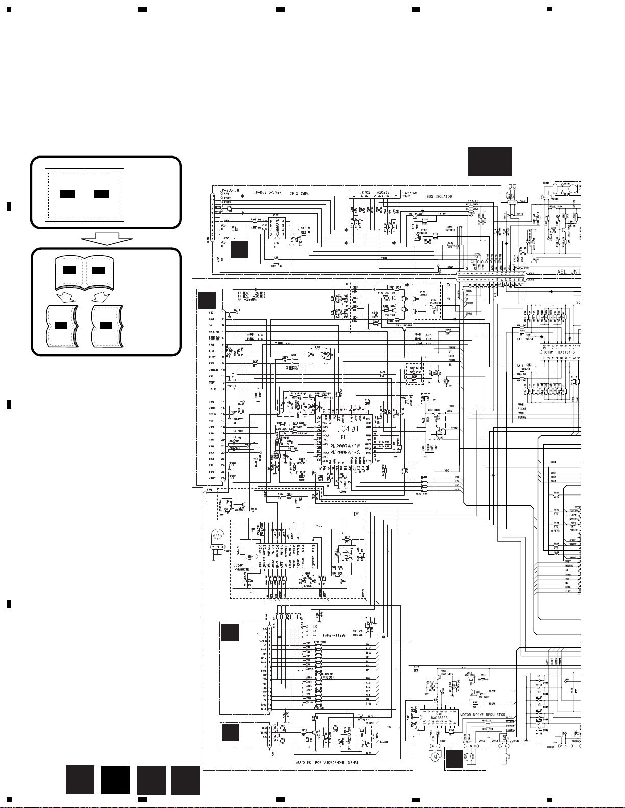
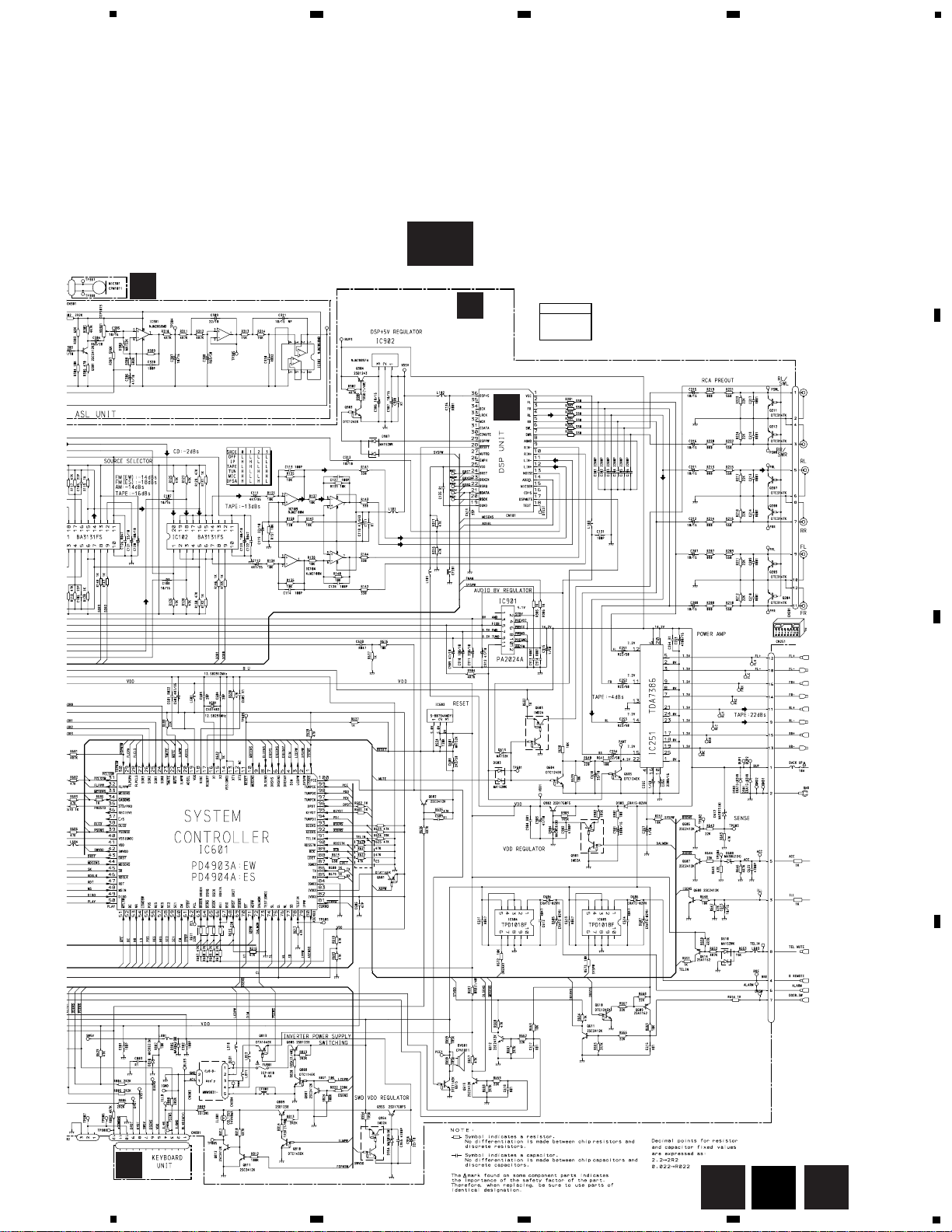
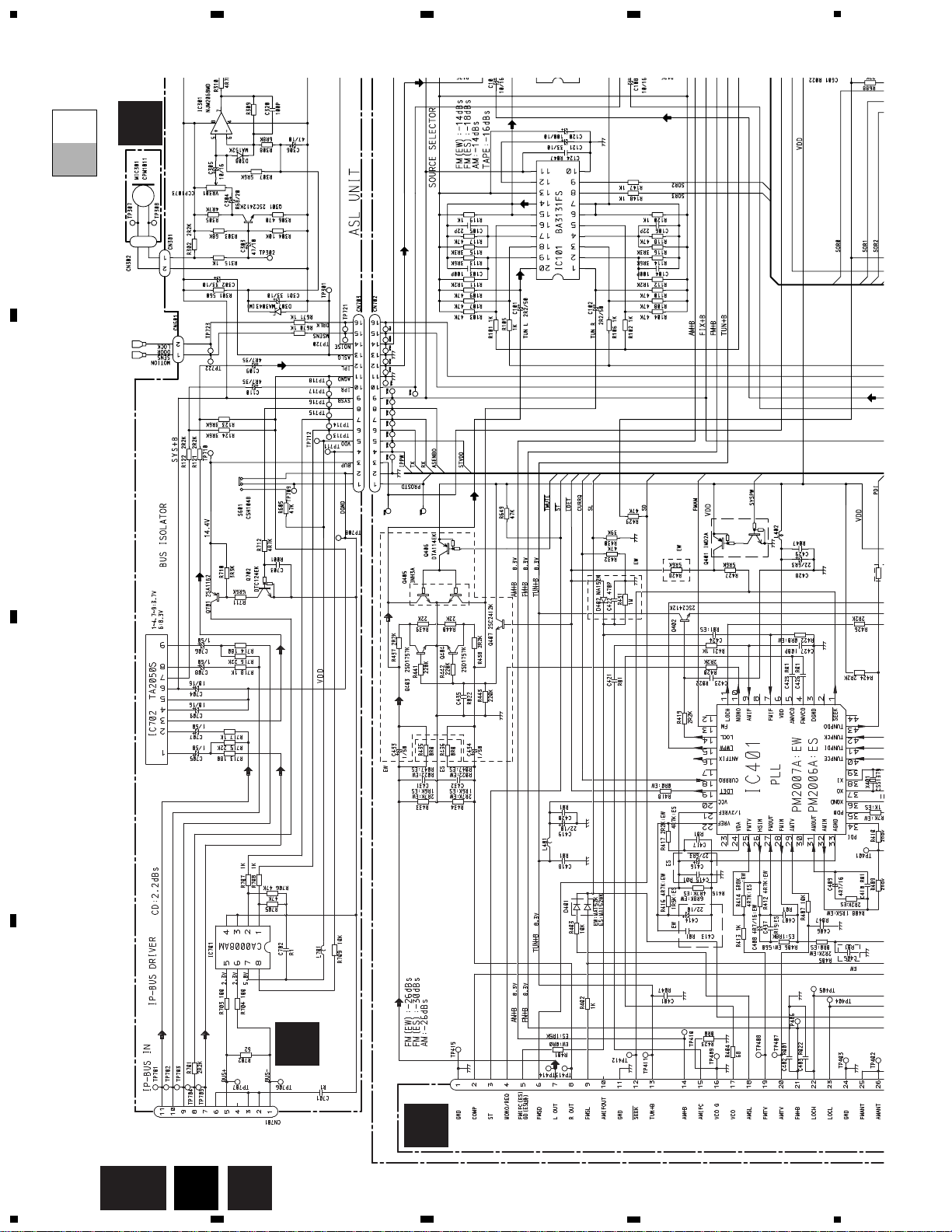
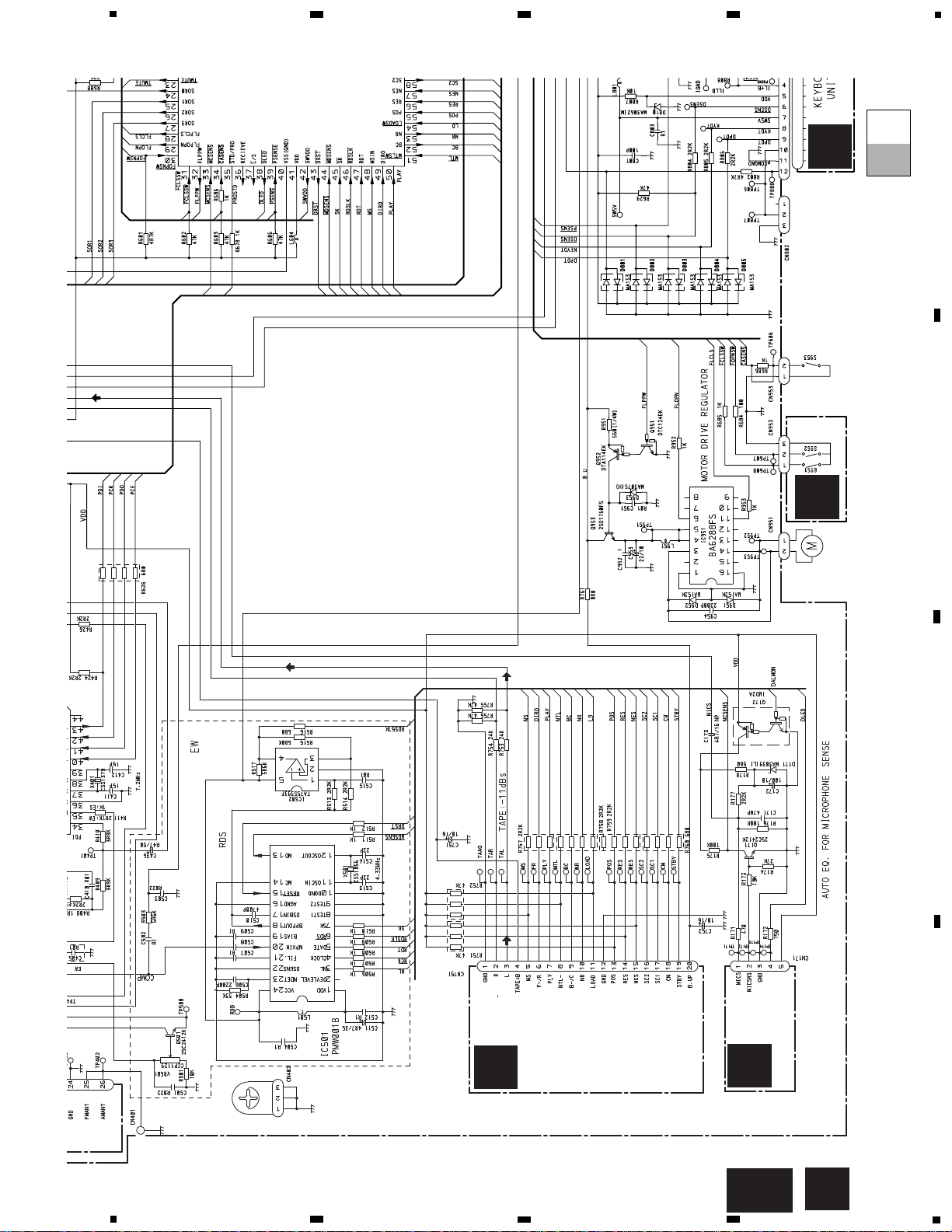
3. SCHEMATIC DIAGRAM
3.1 OVERALL CONNECTION DIAGRAM(GUIDE PAGE)
Note: When ordering service parts, be sure to refer to “EXPLODED VIEWS AND PARTS LIST” or “ELECTRICAL PARTS
LIST”.
A-a A-b
A-a
A-b
A-b
A-a
Large size
SCH diagram
Guide page
Detailed page
10k(B)
22k(B)
REMOTE
CONTROL
INPUT
MIC
JACK
UNIT
G
H
CASSETTE
MECHANISM
MODULE
B
FM/AM TUNER UNIT
C
ASL PCB
K
SWITCH PCB
M951
CXK1085
A-a
A
C
D
K
Page 11
DFS ALARM
UNBALANCE-BALANCE CONVERTER
10k(B)
REMOTE
CONTROL
INPUT
E
D
MIC PCB
A
TUNER AMP UNIT
F
ASL UNIT
Consists of
ASL PCB
MIC PCB
680K
CTH1127
CEK1136
11
KEH-P9700R,P9750
5
6
7
8
A
B
C
D
5
6
7
8
A
A-b
C
D
Page 12
12
KEH-P9700R,P9750
A
1
234
B
C
D
12
34
10k(B)
B
FM/AM TUNER UNIT
C
ASL PCB
D
MIC
680K
A-a
A-a
A-b
C
D
Page 13
13
KEH-P9700R,P9750
5
6
7
8
A
B
C
D
5
6
7
8
22k(B)
REMOTE
CONTROL
INPUT
MIC
JACK
UNIT
G
H
CASSETTE
MECHANISM
MODULE
E
K
SWITCH PCB
M951
CXK1085
A-a
A-a
A-b
K
Page 14
14
KEH-P9700R,P9750
A
1
234
B
C
D
12
34
UNBALANCE-BALANCE CONVERTER
A
TUNER AMP UNIT
F
ASL UNIT
Consists of
ASL PCB
MIC PCB
A-a
A-b
A-b
C
Page 15
15
KEH-P9700R,P9750
5
6
7
8
A
B
C
D
5
6
7
8
DFS ALARM
CTH1127
CEK1136
A-b
A-a
A-b
Page 16
16
KEH-P9700R,P9750
A
1
234
B
C
D
12
34
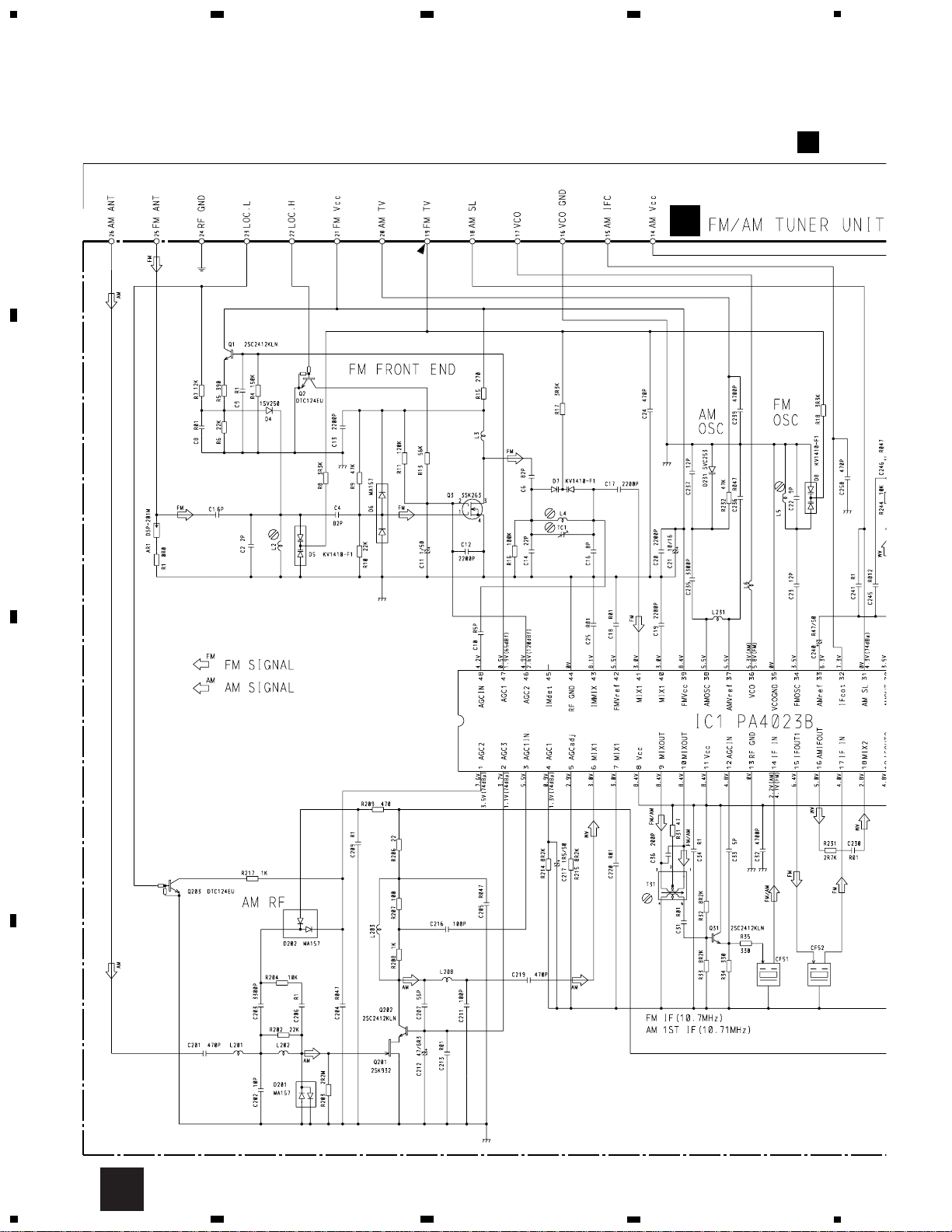
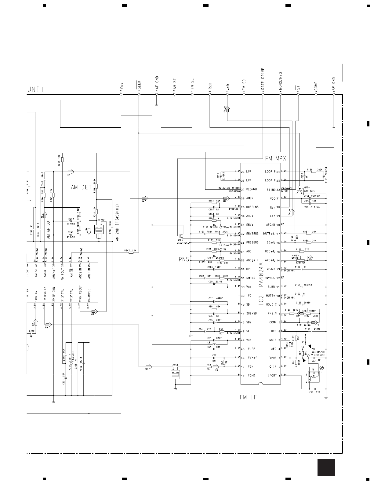
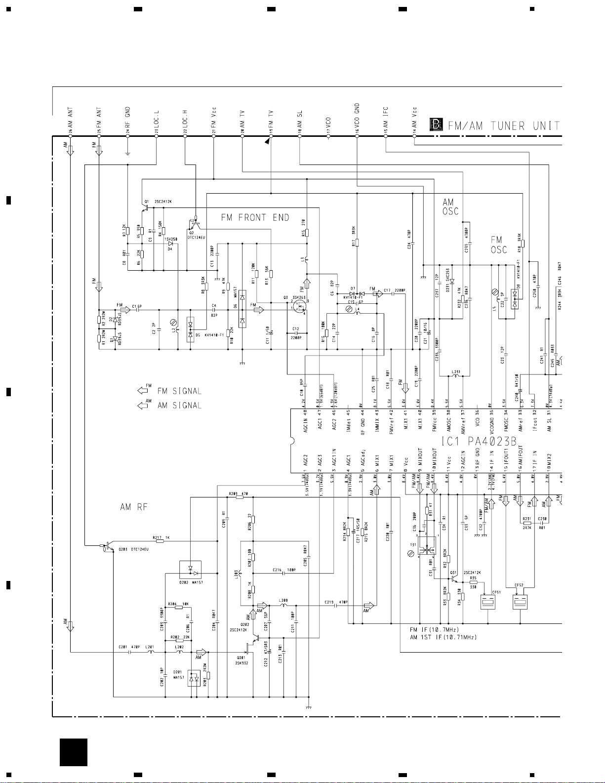
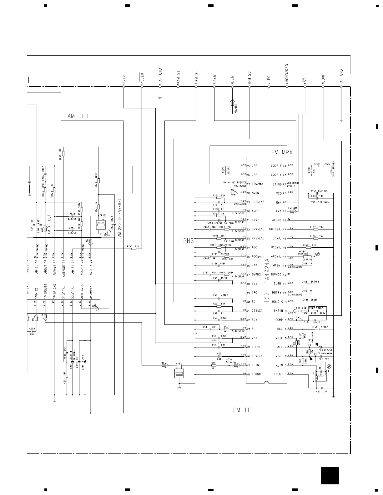
3.2 FM/AM TUNER UNIT
B
- KEH-P9700R/EW
A
B
Page 17
17
KEH-P9700R,P9750
5
6
7
8
A
B
C
D
5
6
7
8
B
Page 18
18
KEH-P9700R,P9750
A
1
234
B
C
D
12
34
B
- KEH-P9750/ES
Page 19
19
KEH-P9700R,P9750
5
6
7
8
A
B
C
D
5
6
7
8
B
Page 20
20
KEH-P9700R,P9750
A
1
234
B
C
D
1
2
34
3.3 CASSETTE MECHANISM MODULE
H
H
A
Page 21
21
KEH-P9700R,P9750
5
6
7
8
A
B
C
D
5
6
7
8
J
I
H
I
J
Page 22
22
KEH-P9700R,P9750
A
1
234
B
C
D
12
34
CAW
E
CL170SBX(ES)
CL170SBX(ES)
CL170PGCD(EW)
CL170DCD(EW)
CL170PGCD(EW)
CL170DCD(EW)
CL170DCD(EW)
CL170SBX(ES)
CL170SBX(ES)
D1906
(ES)
(ES)
(ES)
(ES)
(ES)
(ES)
(ES)
(ES)
(ES)
(ES)
(ES)
(ES)
(EW)
CL170DCD(EW)
(EW)
(EW) (EW)(EW)
LED
ILM
3.4 KEYBOARD UNIT
E
CN801
A
Page 23
CAW1471
23
KEH-P9700R,P9750
5
6
7
8
A
B
C
D
5
6
7
8
E
Page 24
24
KEH-P9700R,P9750
A
1
234
B
C
D
12
34
M.CD:+4.5dBs
FM100%:-1.45dBs
AM30%:-14.45dBs
R3133
0R0
R3132
0R0
R3134
0R0
1K
1K
1K
1K
R3131
0R0
F-a
F
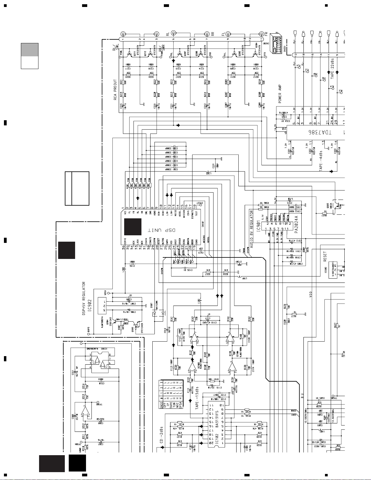
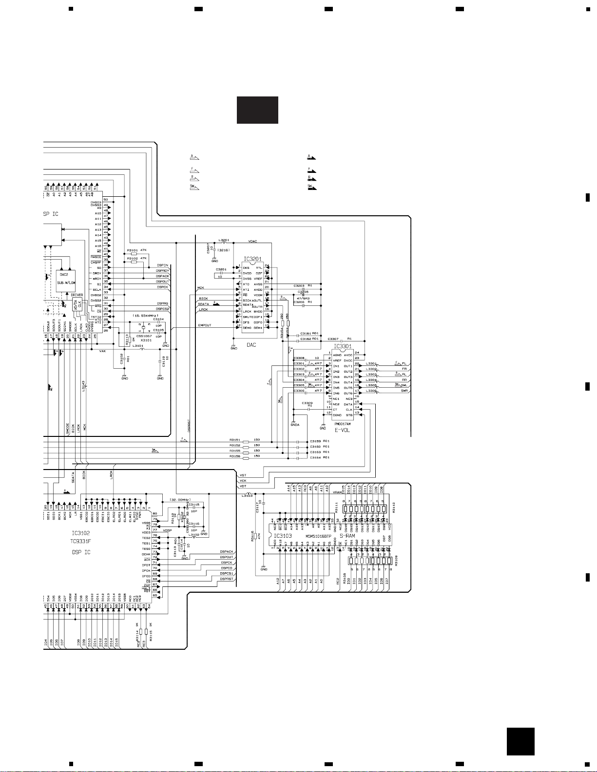
3.5 DSP UNIT(GUIDE PAGE)
A-a A-b
A-a
A-b
A-b
A-a
Large size
SCH diagram
Guide page
Detailed page
Page 25
25
KEH-P9700R,P9750
5
6
7
8
A
B
C
D
5
6
7
8
M.CD:+6.5dBs
FM100%:+0.55dBs
AM30%:-12.45dBs
M,CD:+2.1dBs
FM100%:-4.45dBs
AM30%:-17.45dBs
1k
1k
1k
1k
AK7712AVT(EW)
PE2001AF(ES)
:ANALOG AUDIO INPUT
:FRONT AUDIO OUTPUT(Front/Miid)
:REAR AUDIO OUTPUT(Rear/Hi)
:SUBWOOFER AUDIO OUTPUT
(Sub.w/Low)
:DIGITAL AUDIO
:FRONT AUDIO DIGITAL
:REAR AUDIO DIGITAL
:SUBWOOFER AUDIO DIGITAL
F-b
F
Page 26

26
KEH-P9700R,P9750
A
1
234
B
C
D
12
34
F-a
M.CD:+4.5dBs
FM100%:-1.45dBs
AM30%:-14.45dBs
R3131
0R0
F-a
F-b
Page 27

27
KEH-P9700R,P9750
5
6
7
8
A
B
C
D
5
6
7
8
F-a
1K
1K
1K
1K
R3133
0R0
R3132
0R0
R3134
0R0
F-a
F-b
Page 28

28
KEH-P9700R,P9750
A
1
234
B
C
D
12
34
M.CD:+6.5dBs
FM100%:+0.55dBs
AM30%:-12.45dBs
M.CD:+2.1dBs
FM100%:-4.45dBs
AM30%:-17.45dBs
:ANALOG AUDIO INPUT
:FRONT AUDIO OUTPUT(Front/Miid)
:REAR AUDIO OUTPUT(Rear/Hi)
:SUBWOOFER AUDIO OUTPUT
(Sub.w/Low)
:DIGITAL AUDIO
:FRONT AUDIO DIGITAL
:REAR AUDIO DIGITAL
:SUBWOOFER AUDIO DIGITAL
AK4321VF(EW)
PE2001AF(ES)
F-b
F-a
F-b
Page 29

29
KEH-P9700R,P9750
5
6
7
8
A
B
C
D
5
6
7
8
1K
1K
1K
1K
R01
F-b
F-a
F-b
Page 30

30
KEH-P9700R,P9750
A
1
234
B
C
D
12
34
G
3.6 MIC JACK UNIT
G
A
CN171
Page 31

31
KEH-P9700R,P9750
1
2
3
4
A
B
C
D
1
2
3
4. PCB CONNECTION DIAGRAM
4.1 MIC JACK UNIT
NOTE FOR PCB DIAGRAMS
1. The parts mounted on this PCB
include all necessary parts for
several destination.
For further information for
respective destinations, be sure
to check with the schematic
diagram.
2. Viewpoint of PCB diagrams
CLOSE
S951
OPEN
S952
3
2
1
CN952
A
4.2 SWITCH PCB
CN171
A
K
G
SIDE A
SIDE B
4
Connector
P.C.Board
Capacitor
Chip Part
SIDE A
SIDE B
Page 32

32
KEH-P9700R,P9750
A
1
234
B
C
D
12
34
4.3 TUNER AMP UNIT
A
A
F
CN4601
G
CN3001
CARD ASSY
K
TUNER AMP UNIT
Page 33

33
KEH-P9700R,P9750
5
6
7
8
A
B
C
D
5
6
7
8
A
SIDE A
CN251
H
CN703
C
CN1901
E
B
Page 34

34
KEH-P9700R,P9750
A
1
234
B
C
D
12
34
A
A
TUNER AMP UNIT
Page 35

35
KEH-P9700R,P9750
5
6
7
8
A
B
C
D
5
6
7
8
A
SIDE B
Page 36

KEH-P9700R,P9750
A
1
234
B
C
D
12
34
4.4 KEYBOARD UNIT
E
E
KEYBOARD UNIT
36
E
KEYBOARD UNIT
CN801
A
Page 37

37
KEH-P9700R,P9750
5
6
7
8
A
B
C
D
5
6
7
8
E
SIDE A
SIDE B
Page 38

38
KEH-P9700R,P9750
A
1
234
B
C
D
1
2
34
4.5 DSP UNIT
F
SIDE A
DSP UNIT
F
Page 39

39
KEH-P9700R,P9750
5
6
7
8
A
B
C
D
5
6
7
8
F
SIDE B
DSP UNIT
F
CN101
A
Page 40

40
KEH-P9700R,P9750
A
1
234
B
C
D
12
34
4.6 FM/AM TUNER UNIT
B
SIDE A
FM/AM TUNET UNIT
A
B
Page 41

41
KEH-P9700R,P9750
5
6
7
8
A
B
C
D
5
6
7
8
B
SIDE B
FM/AM TUNET UNIT
B
Page 42

42
KEH-P9700R,P9750
A
1
234
B
C
D
1
2
34
4.7 CASSETTE MECHANISM MODULE
H
H
A
DECK UNIT
I
Page 43

43
KEH-P9700R,P9750
5
6
7
8
A
B
C
D
5
6
7
8
J
I
I
PCB UNIT
J
REEL PCB
I
PCB UNIT
SIDE A
SIDE B
H
J
I
Page 44

44
KEH-P9700R,P9750
A
1
234
B
C
D
12
34
4.8 ASL UNIT
SIDE A
SIDE B
ASL PCB
C
ASL PCB
SIDE A
SIDE B
MIC PCB
C
CN601
D
CN302
A
CN702
C
D
C
D
Page 45

45
KEH-P9700R,P9750
5. ELECTRICAL PARTS LIST
NOTE:
- Parts whose parts numbers are omitted are subject to being not supplied.
- The part numbers shown below indicate chip components.
Chip Resistor
RS1/_S___J,RS1/__S___J
Chip Capacitor (except for CQS.....)
CKS....., CCS....., CSZS.....
R 8 RS1/16S332J
R 9 RS1/16S473J
R 10 RS1/16S223J
R 11 RS1/16S124J
R 13 RS1/16S563J
R 15 RS1/16S271J
R 16 RS1/16S104J
R 17 RS1/16S332J
R 18 RS1/16S332J
R 31 RS1/16S470J
R 32 RS1/16S822J
R 33 RS1/16S822J
R 34 RS1/16S331J
R 35 RS1/16S331J
R 51 RS1/16S271J
R 52 RS1/16S560J
R 55 RS1/16S102J
R 56 RS1/16S823J
R 61 RS1/16S392J
R 62 RS1/16S393J
R 101 RS1/16S272J
R 102 RS1/16S682J
R 103 RS1/16S333J
R 104 RS1/16S334J
R 105 RS1/16S683J
R 107 RS1/16S222J
R 151 RS1/16S222J
R 152 RS1/16S393J
R 154 RS1/16S104J
R 155 RS1/16S273J
R 156 RS1/16S243J
R 157 RS1/16S203J
R 160 RS1/16S222J
R 161 RS1/16S563J
R 162 RS1/16S105J
R 163 RS1/16S222J
R 202 RS1/16S223J
R 203 RS1/16S225J
R 204 RS1/16S103J
R 206 RS1/16S220J
R 207 RS1/16S101J
R 208 RS1/16S102J
R 209 RS1/16S471J
R 214 RS1/16S822J
R 215 RS1/16S822J
R 217 RS1/16S102J
R 231 RS1/16S272J
R 232 RS1/16S473J
R 237 RS1/16S103J
R 238 RS1/16S104J
R 239 RS1/16S104J
R 240 RS1/16S332J
R 241 RS1/16S202J
R 243 RS1/16S123J
R 244 RS1/16S103J
Unit Number : CWE1416(EW)
Unit Name : FM/AM Tuner Unit
MISCELLANEOUS
IC 1 IC PA4023B
IC 2 IC PA4024A
Q 1 Transistor 2SC2412K
Q 2 Transistor DTC124EU
Q 3 FET 3SK263
Q 31 Transistor 2SC2412K
Q 154 Transistor DTC124EU
Q 165 Transistor 2SC2412K
Q 201 FET 2SK932
Q 202 Transistor 2SC2412K
Q 203 Transistor DTC124EU
D 4 Diode 1SV250
D 5 Diode KV1410-F1
D 7 Diode KV1410-F1
D 8 Diode KV1410-F1
D 201 Diode MA157
D 202 Diode MA157
D 231 Diode SVC253
L 2 Coil CTC1108
L 3 Inductor LCTB2R2K2125
L 4 Coil CTC1108
L 5 Coil CTC1107
L 6 Inductor LCTBR15K1608
L 51 Ferri-Inductor LAU150K
L 201 Ferri-Inductor LAU4R7K
L 202 Ferri-Inductor LAU330K
L 203 Inductor CTF1287
L 208 Inductor LAU121K
L 231 Inductor LCTA3R3J3225
T 31 Coil CTE1116
T 51 Coil CTC1136
TC 1 CCL1046
CF 51 Ceramic Filter CTF1292
CF 52 Ceramic Filter CTF1292
CF 53 Ceramic Filter CTF1292
CF 232 Ceramic Filter CTF1348
X 151 918.5Hz CSS1365
X 231 Crystal Resonator 10.26MHz CSS1111
VR 154 Semi-fixed 150kΩ(B) CCP1213
AR 1 DSP-201M
RESISTORS
R 1 RS1/16S0R0J
R 4 RS1/16S154J
R 5 RS1/16S391J
R 6 RS1/16S223J
R 7 RS1/16S123J
=====Circuit Symbol & No.===Part Name Part No.
--- ------ ------------------------------------------ -------------------------
=====Circuit Symbol & No.===Part Name Part No.
--- ------ ------------------------------------------ -------------------------
B
Page 46

46
KEH-P9700R,P9750
R 247 RS1/16S123J
CAPACITORS
C 1 CCSQCH6R0D50
C 2 CCSRCK2R0C50
C 4 CCSRCH820J50
C 6 CCSRCH820J50
C 8 CKSRYB103K25
C 9 CKSQYB104K16
C 10 CCSRCKR50C50
C 11 CEJA1R0M50
C 12 CCSRCH100D50
C 13 CKSRYB222K50
C 14 CCSRCH220J50
C 16 CCSRCH8R0D50
C 17 CKSRYB222K50
C 18 CKSRYB103K25
C 19 CKSRYB222K50
C 20 CKSRYB222K50
C 21 CEJA100M16
C 22 CCSRTH9R0D50
C 23 CCSRTH120J50
C 24 CCSRCH471J50
C 25 CKSRYB103K25
C 31 CKSRYB103K25
C 32 CKSQYB472K50
C 33 CCSRCH5R0C50
C 34 CKSQYB104K16
C 36 CCSRRH201J50
C 51 CKSRYB223K25
C 52 CKSRYB103K25
C 54 CCSRCH470J50
C 55 CKSQYB223K25
C 56 CKSQYB104K16
C 57 CKSRYB472K50
C 58 CEJA330M10
C 59 CKSRYB103K25
C 61 CCSRCH270J50
C 62 CKSRYB103K25
C 63 CEJAR15M50
C 101 CEJANP100M10
C 102 CKSRYB182K50
C 103 CKSRYB682K25
C 104 CEJA2R2M50
C 105 CKSRYB103K25
C 106 CCSRCH151J50
C 107 CKSRYB103K25
C 151 CKSRYB472K50
C 152 CKSQYB104K16
C 153 CEJA3R3M50
C 154 CKSQYB104K16
C 157 CEJA3R3M50
C 158 CKSYB474K16
C 159 CEJA220M6R3
C 160 CKSQYB104K16
C 161 CKSQYB104K16
C 162 CEJA3R3M50
C 163 CKSRYB102K50
C 170 CCSRCH100D50
C 201 CCSRCH471J50
C 202 CCSRCH100D50
C 203 CKSRYB332K50
C 204 CKSQYB473K16
C 205 CKSQYB473K16
C 206 CKSQYB104K16
C 207 CCSRCH560J50
C 209 CKSQYB104K16
C 211 CCSRCH101J50
C 212 CEJA470M6R3
C 213 CKSRYB103K25
C 216 CCSRCH101J50
C 217 CEJA1R5M50
C 219 CCSRCH471J50
C 220 CKSRYB103K25
C 230 CKSRYB103K25
C 231 CCSRCH330J50
C 232 CCSRCH150J50
C 233 CKSQYB104K16
C 234 CEJA330M10
C 235 CKSRYB332K50
C 236 CKSQYB473K16
C 237 CCSRCH120J50
C 239 CKSRYB472K50
C 240 CEJAR47M50
C 241 CKSQYB104K16
C 242 CEJAR47M50
C 243 CEJAR33M50
C 244 CKSQYB473K16
C 245 CKSRYB123K25
C 246 CKSQYB473K16
C 250 CCSRCH471J50
Unit Number : CWE1485(ES)
Unit Name : FM/AM Tuner Unit
MISCELLANEOUS
IC 1 IC PA4023B
IC 2 IC PA4024A
Q 1 Transistor 2SC2412KLN
Q 2 Transistor DTC124EU
Q 3 FET 3SK263
Q 31 Transistor 2SC2412KLN
Q 201 FET 2SK932
Q 202 Transistor 2SC2412KLN
Q 203 Transistor DTC124EU
D 1 Diode RD39JS
D 2 Diode RD39JS
D 4 Diode 1SV250
D 5 Diode KV1410-F1
D 6 Diode MA157
D 7 Diode KV1410-F1
D 8 Diode KV1410-F1
D 201 Diode MA157
D 202 Diode MA157
D 231 Diode SVC253
L 2 Coil CTC1108
L 3 Inductor LCTB2R2K2125
L 4 Coil CTC1108
L 5 Coil CTC1107
L 6 Inductor LCTBR15K1608
L 51 Ferri-Inductor LAU150K
L 201 Ferri-Inductor LAU4R7K
L 202 Ferri-Inductor LAU330K
L 203 Inductor CTF1287
L 208 Inductor LAU121K
L 231 Inductor LCTA3R3J3225
T 31 Coil CTE1117-B-TX
T 51 Coil CTC1136-A-TX
CF 51 Ceramic Filter CTF1290
CF 52 Ceramic Filter CTF1290
CF 53 Ceramic Filter CTF1290
CF 232 Ceramic Filter CTF1348
X 151 918.5Hz CSS1365
X 231 Crystal Resonator 10.26MHz CSS1111
VR 154 Semi-fixed 150kΩ(B) CCP1213
=====Circuit Symbol & No.===Part Name Part No.
--- ------ ------------------------------------------ -------------------------
=====Circuit Symbol & No.===Part Name Part No.
--- ------ ------------------------------------------ -------------------------
B
Page 47

47
KEH-P9700R,P9750
RESISTORS
R 1 RS1/16S225J
R 2 RS1/16S225J
R 4 RS1/16S154J
R 5 RS1/16S391J
R 6 RS1/16S223J
R 7 RS1/16S123J
R 8 RS1/16S332J
R 9 RS1/16S473J
R 10 RS1/16S223J
R 11 RS1/16S124J
R 13 RS1/16S563J
R 15 RS1/16S271J
R 16 RS1/16S104J
R 17 RS1/16S332J
R 18 RS1/16S332J
R 31 RS1/16S470J
R 32 RS1/16S822J
R 33 RS1/16S822J
R 34 RS1/16S331J
R 35 RS1/16S331J
R 51 RS1/16S271J
R 52 RS1/16S560J
R 55 RS1/16S102J
R 56 RS1/16S823J
R 61 RS1/16S392J
R 62 RS1/16S273J
R 101 RS1/16S272J
R 102 RS1/16S682J
R 103 RS1/16S333J
R 104 RS1/16S334J
R 105 RS1/16S683J
R 107 RS1/16S222J
R 151 RS1/16S222J
R 152 RS1/16S393J
R 155 RS1/16S273J
R 156 RS1/16S243J
R 157 RS1/16S203J
R 160 RS1/16S222J
R 161 RS1/16S563J
R 162 RS1/16S105J
R 163 RS1/16S223J
R 202 RS1/16S223J
R 203 RS1/16S225J
R 204 RS1/16S103J
R 206 RS1/16S220J
R 207 RS1/16S101J
R 208 RS1/16S102J
R 209 RS1/16S471J
R 214 RS1/16S822J
R 215 RS1/16S822J
R 217 RS1/16S102J
R 231 RS1/16S272J
R 232 RS1/16S473J
R 237 RS1/16S103J
R 238 RS1/16S104J
R 239 RS1/16S104J
R 240 RS1/16S332J
R 241 RS1/16S202J
R 243 RS1/16S183J
R 244 RS1/16S392J
R 247 RS1/16S123J
CAPACITORS
C 1 CCSQCH6R0D50
C 2 CCSRCK2R0C50
C 4 CCSRCH820J50
C 6 CCSRCH820J50
C 8 CKSRYB103K25
C 9 CKSQYB104K16
C 10 CCSRCKR50C50
C 11 CEJA1R0M50
C 12 CKSRYB222K50
C 13 CKSRYB222K50
C 14 CCSRCH220J50
C 15 CCSRCH6R0D50
C 16 CCSRCH8R0D50
C 17 CKSRYB222K50
C 18 CKSRYB103K25
C 19 CKSRYB222K50
C 20 CKSRYB222K50
C 21 CEJA100M16
C 22 CCSRTH9R0D50
C 23 CCSRTH120J50
C 24 CCSRCH471J50
C 25 CKSRYB103K25
C 31 CKSRYB103K25
C 32 CKSQYB472K50
C 33 CCSRCH5R0C50
C 34 CKSQYB104K16
C 36 CCSRRH201J50
C 51 CKSRYB223K25
C 52 CKSRYB103K25
C 54 CCSRCH470J50
C 55 CKSQYB223K25
C 56 CKSQYB104K16
C 57 CKSRYB472K50
C 58 CEJA330M10
C 59 CKSRYB103K25
C 60 CKSRYB102K50
C 61 CCSRCH270J50
C 62 CKSRYB103K25
C 63 CEJAR22M50
C 101 CEJANP100M10
C 102 CKSRYB182K50
C 103 CKSRYB682K25
C 104 CEJA2R2M50
C 105 CKSRYB103K25
C 106 CCSRCH151J50
C 107 CKSRYB103K25
C 151 CKSRYB472K50
C 152 CKSQYB104K16
C 153 CEJA3R3M50
C 154 CKSQYB104K16
C 157 CEJA3R3M50
C 158 CKSYB474K16
C 159 CEJA220M6R3
C 160 CKSQYB104K16
C 161 CKSQYB104K16
C 162 CEJA3R3M50
C 163 CKSRYB102K50
C 170 CCSRCH100D50
C 201 CCSRCH471J50
C 202 CCSRCH100D50
C 203 CKSRYB332K50
C 204 CKSQYB473K16
C 205 CKSQYB473K16
C 206 CKSQYB104K16
C 207 CCSRCH560J50
=====Circuit Symbol & No.===Part Name Part No.
--- ------ ------------------------------------------ -------------------------
=====Circuit Symbol & No.===Part Name Part No.
--- ------ ------------------------------------------ -------------------------
Page 48

48
KEH-P9700R,P9750
C 209 CKSQYB104K16
C 211 CCSRCH101J50
C 212 CEJA470M6R3
C 213 CKSRYB103K25
C 216 CCSRCH101J50
C 217 CEJA1R5M50
C 219 CCSRCH471J50
C 220 CKSRYB103K25
C 230 CKSRYB103K25
C 231 CCSRCH330J50
C 232 CCSRCH150J50
C 233 CKSQYB104K16
C 234 CEJA330M10
C 235 CKSRYB332K50
C 236 CKSQYB473K16
C 237 CCSRCH120J50
C 239 CKSRYB472K50
C 240 CEJAR47M50
C 241 CKSQYB104K16
C 242 CEJAR47M50
C 243 CEJAR33M50
C 244 CKSQYB473K16
C 245 CKSRYB333K16
C 246 CKSQYB473K16
C 250 CCSRCH471J50
Unit Number : CWM5781(EW)
CWM5782(ES)
Unit Name : Tuner Amp Unit
MISCELLANEOUS
IC 101 IC BA3131FS
IC 102 IC BA3131FS
IC 103 IC NJM2100M
IC 104 IC NJM2100M
IC 251 IC TDA7386
IC 401 IC
See Contrast Table
IC 501 IC See Contrast Table
IC 502 IC See Contrast Table
IC 601 IC See Contrast Table
IC 602 IC S-80734ANDYI
IC 604 IC TPD1018F
IC 605 IC TPD1018F
IC 901 IC PA2024A
IC 902 IC NJM7805FA
IC 951 IC BA6288FS
Q 171 Transistor 2SC2412K
Q 172 Transistor IMD2A
Q 203 Transistor DTC314TK
Q 204 Transistor DTC314TK
Q 207 Transistor DTC314TK
Q 208 Transistor DTC314TK
Q 211 Transistor DTC314TK
Q 212 Transistor DTC314TK
Q 401 Transistor IMD2A
Q 402 Transistor 2SC2412K
Q 403 Transistor
See Contrast Table
Q 404 Transistor See Contrast Table
Q 405 Transistor See Contrast Table
Q 406 Transistor See Contrast Table
Q 407 Transistor See Contrast Table
Q 501 Transistor See Contrast Table
Q 601 Transistor DTA114EK
Q 602 Transistor 2SC2412K
Q 603 Transistor IMD2A
Q 604 Transistor DTC124EK
Q 605 Transistor DTC124EK
Q 606 Transistor 2SC2412K
Q 607 Transistor 2SC2412K
Q 608 Transistor 2SC2412K
Q 609 Transistor 2SA1162
Q 610 Transistor DTC124EK
Q 611 Transistor 2SC2412K
Q 612 Transistor 2SC2412K
Q 613 Transistor 2SC2412K
Q 614 Transistor 2SA1162
Q 615 Transistor DTC114EK
Q 805 Transistor 2SB1238
Q 807 Transistor 2SC2412K
Q 808 Transistor DTC114EK
Q 809 Transistor 2SB1238
Q 810 Transistor DTC143EK
Q 811 Transistor 2SC2412K
Q 812 Transistor 2SC2412K
Q 813 Transistor DTA144EK
Q 901 Transistor IMD2A
Q 902 Transistor 2SD1760F5
Q 903 Transistor DTC124EK
Q 904 Transistor 2SB1243
Q 951 Transistor DTC124EK
Q 952 Transistor DTA114EK
Q 953 Transistor 2SD1760F5
Q 954 Transistor IMD2A
Q 955 Transistor 2SD1760F5
D 171 Diode MA3039(L)
D 401 Diode
See Contrast Table
D 402 Diode See Contrast Table
D 601 Diode MA152K
D 603 Diode MA152WK
D 604 Diode ERA15-02VH
D 605 Diode ERA15-02VH
D 606 Diode ERA15-02VH
D 607 Diode ERA15-02VH
D 608 Diode MA3062(H)
D 610 Diode MA152WK
D 612 Diode MA3075(M)
D 613 Diode MA152K
D 801 Diode MA153
D 802 Diode MA153
D 803 Diode MA153
D 804 Diode MA153
D 805 Diode MA153
D 806 Diode MA3062(M)
D 810 Diode MA3062(M)
D 901 Diode ERA15-02VH
D 902 Diode ERA15-02VH
D 903 Diode ERA15-02VH
D 904 Diode MA3056(M)
D 907 Diode MA152WK
D 951 Diode MA152K
D 952 Diode MA152K
D 953 Diode MA3075(H)
D 954 Diode MA3056(M)
L 101 Inductor LCTA2R2J3225
L 102 Inductor LCTA2R2J3225
L 103 Inductor CTF1420
L 401 Ferri-Inductor LAU2R2K
L 402 Ferri-Inductor LAU2R2K
L 501 Ferri-Inductor
See Contrast Table
L 601 Ferri-Inductor LAU2R2K
L 603 Inductor LCTA2R2J3225
=====Circuit Symbol & No.===Part Name Part No.
--- ------ ------------------------------------------ -------------------------
=====Circuit Symbol & No.===Part Name Part No.
--- ------ ------------------------------------------ -------------------------
A
Page 49

49
KEH-P9700R,P9750
L 604 Inductor CTF1420
L 801 Ferri-Inductor LAU2R2K
L 810 Inductor CTF1420
L 811 Inductor CTF1420
L 812 Inductor CTF1420
L 901 Inductor LCTB2R2K3216
CF 201 Filter CTF1071
X 401 Crystal Resonator 7.200MHz CSS1379
X 501 Crystal Resonator
See Contrast Table
X 601 12.58291MHz CSS1402
IL 801 Lamp 14V40mA CEL1359
VR 501 Semi-fixed See Contrast Table
FU 801 Fuze 0.4A ICP-N10
BV 601 Buzzer CPV1011
DSP Unit CWX2237
ASL Unit CWM5783
FM/AM Tuner Unit
See Contrast Table
RESISTORS
R 101 RS1/10S102J
R 102 RS1/10S102J
R 103 RS1/10S473J
R 104 RS1/10S473J
R 105 RS1/10S102J
R 106 RS1/10S102J
R 107 RS1/10S473J
R 108 RS1/10S473J
R 109 RS1/10S473J
R 110 RS1/10S473J
R 111 RS1/10S122J
R 112 RS1/10S122J
R 113 RS1/10S362J
R 114 RS1/10S362J
R 115 RS1/10S332J
R 116 RS1/10S332J
R 117 RS1/10S473J
R 118 RS1/10S473J
R 119 RS1/10S102J
R 120 RS1/10S102J
R 125 RS1/10S473J
R 126 RS1/10S473J
R 127 RS1/10S473J
R 128 RS1/10S473J
R 129 RS1/10S473J
R 130 RS1/10S473J
R 131 RS1/10S102J
R 132 RS1/10S102J
R 133 RS1/10S103J
R 134 RS1/10S103J
R 135 RS1/10S103J
R 136 RS1/10S103J
R 137 RS1/10S103J
R 138 RS1/10S103J
R 139 RS1/10S103J
R 140 RS1/10S103J
R 141 RS1/10S331J
R 142 RS1/10S331J
R 143 RS1/10S331J
R 144 RS1/10S331J
R 145 RS1/16S102J
R 146 RS1/16S102J
R 147 RS1/16S102J
R 148 RS1/16S102J
R 149 RS1/10S103J
R 150 RS1/10S121J
R 151 RS1/10S103J
R 171 RS1/10S471J
R 172 RS1/8S751J
R 173 RS1/10S103J
R 174 RS1/10S273J
R 175 RS1/10S104J
R 176 RS1/10S104J
R 177 RS1/10S222J
R 178 RS1/10S561J
R 201 RS1/10S331J
R 202 RS1/10S331J
R 203 RS1/10S331J
R 204 RS1/10S331J
R 205 RS1/10S331J
R 206 RS1/10S331J
R 207 RS1/10S0R0J
R 208 RS1/10S0R0J
R 209 RS1/10S561J
R 210 RS1/10S561J
R 211 RS1/10S223J
R 212 RS1/10S223J
R 213 RS1/10S0R0J
R 214 RS1/10S0R0J
R 215 RS1/10S561J
R 216 RS1/10S561J
R 217 RS1/10S223J
R 218 RS1/10S223J
R 219 RS1/10S0R0J
R 220 RS1/10S0R0J
R 221 RS1/10S561J
R 222 RS1/10S561J
R 223 RS1/10S223J
R 224 RS1/10S223J
R 251 RS1/10S103J
R 316 RN1/10SE4702D
R 317 RN1/10SE4702D
R 401
See Contrast Table
R 402 RS1/10S102J
R 403 RS1/10S103J
R 404 RS1/10S680J
R 405
See Contrast Table
R 406 See Contrast Table
R 407 RS1/10S103J
R 408
See Contrast Table
R 409 RS1/10S392J
R 410 RS1/16S392J
R 411
See Contrast Table
R 412 See Contrast Table
R 413 RS1/10S102J
R 414
See Contrast Table
R 415 See Contrast Table
R 416 See Contrast Table
R 417 See Contrast Table
R 418 See Contrast Table
R 419 RS1/10S222J
R 420 RS1/16S222J
R 421 RS1/16S102J
R 422
See Contrast Table
R 423 RS1/10S0R0J
R 424 RS1/16S222J
R 426 RS1/16S222J
R 427 RS1/16S562J
R 428
See Contrast Table
R 429 RS1/16S473J
=====Circuit Symbol & No.===Part Name Part No.
--- ------ ------------------------------------------ -------------------------
=====Circuit Symbol & No.===Part Name Part No.
--- ------ ------------------------------------------ -------------------------
Page 50

50
KEH-P9700R,P9750
R 430 RS1/16S393J
R 431
See Contrast Table
R 432 RS1/10S473J
R 433
See Contrast Table
R 434 See Contrast Table
R 435 See Contrast Table
R 436 See Contrast Table
R 437 See Contrast Table
R 438 See Contrast Table
R 439 See Contrast Table
R 440 See Contrast Table
R 441 See Contrast Table
R 442 RS1/16S224J
R 443
See Contrast Table
R 501 See Contrast Table
R 503 See Contrast Table
R 504 See Contrast Table
R 506 See Contrast Table
R 507 See Contrast Table
R 508 See Contrast Table
R 509 See Contrast Table
R 510 See Contrast Table
R 511 See Contrast Table
R 512 See Contrast Table
R 513 See Contrast Table
R 514 See Contrast Table
R 515 See Contrast Table
R 516 See Contrast Table
R 517 See Contrast Table
R 601 RS1/16S472J
R 602 RS1/16S473J
R 603 RS1/10S473J
R 606 RS1/16S473J
R 607 RS1/16S473J
R 608 RS1/16S473J
R 609 RS1/16S473J
R 610 RS1/16S473J
R 611 RA4C221J
R 615 RS1/16S221J
R 616 RS1/16S473J
R 617 RS1/16S473J
R 618 RS1/16S473J
R 619 RS1/16S681J
R 620
See Contrast Table
R 621 See Contrast Table
R 622 See Contrast Table
R 623 RS1/16S473J
R 624 RS1/16S393J
R 625 RS1/16S473J
R 626 RA4C681J
R 627 RS1/16S102J
R 628 RS1/16S473J
R 629 RS1/16S473J
R 630 RS1/16S473J
R 632 RS1/16S102J
R 634 RS1/16S124J
R 635 RS1/16S473J
R 636 RS1/10S472J
R 637 RS1/10S102J
R 638 RS1/10S103J
R 639 RS1/10S103J
R 640 RS1/10S221J
R 641 RS1/10S101J
R 642 RS1/16S223J
R 643 RS1/16S473J
R 644 RS1/16S223J
R 645 RS1/16S473J
R 646 RS1/10S472J
R 647 RS1/10S473J
R 648 RS1/10S103J
R 649 RS1/16S473J
R 650 RS1/16S472J
R 651 RS1/16S102J
R 652 RS1/16S472J
R 653 RS1/8S153J
R 654 RS1/10S102J
R 655 RS1/16S152J
R 656 RS1/16S152J
R 657 RS1/16S473J
R 658 RS1/16S272J
R 659 RS1/16S223J
R 660 RS1/16S473J
R 661 RS1/16S272J
R 662 RS1/16S223J
R 663 RS1/16S103J
R 664 RS1/16S473J
R 665 RS1/16S272J
R 666 RS1/16S223J
R 667 RS1/16S223J
R 668 RS1/16S223J
R 669 RS1/16S103J
R 672 RS1/10S103J
R 673 RS1/10S103J
R 676 RS1/10S103J
R 677 RS1/10S102J
R 678 RS1/16S102J
R 679 RS1/16S102J
R 680 RS1/16S102J
R 681 RS1/16S102J
R 682 RS1/16S102J
R 683 RS1/16S473J
R 684 RS1/16S101J
R 685 RS1/16S102J
R 686 RS1/16S102J
R 687 RS1/4S0R0J
R 688 RS1/16S223J
R 751 RA3C473J
R 752 RA3C473J
R 753 RS1/10S243J
R 754 RS1/10S243J
R 755 RS1/10S473J
R 756 RS1/10S473J
R 757 RA3C222J
R 758 RA4C222J
R 759 RA4C222J
R 760 RA4C681J
R 761 RS1/10S0R0J
R 802 RS1/8S472J
R 804 RS1/8S222J
R 805 RS1/8S222J
R 806 RS1/8S222J
R 807 RS1/16S103J
R 808 RS1/8S222J
R 809 RS2PMF330J
R 810 RS1/10S472J
R 811 RS1/10S1R0J
R 812 RS1/10S104J
R 813 RS1/10S222J
R 814 RS1/4S152J
R 820 RS1/4S152J
=====Circuit Symbol & No.===Part Name Part No.
--- ------ ------------------------------------------ -------------------------
=====Circuit Symbol & No.===Part Name Part No.
--- ------ ------------------------------------------ -------------------------
Page 51

51
KEH-P9700R,P9750
R 821 RS1/10S103J
R 822 RS1/10S224J
R 823 RS1/10S222J
R 824 RS1/10S104J
R 901 RS1/10S101J
R 902 RS1/10S152J
R 903 RS1/10S752J
R 904 RS1/16S472J
R 905 RS1/16S102J
R 906 RS1/16S102J
R 907 RS1/10S472J
R 908 RS1/4S152J
R 951 RS1/4S561J
R 952 RS1/10S102J
R 953 RS1/10S102J
R 954 RS1/10S152J
CAPACITORS
C 101 CEV2R2M50
C 102 CEV2R2M50
C 103 CCSQCH101J50
C 104 CCSQCH101J50
C 105 CCSQCH220J50
C 106 CCSQCH220J50
C 107 CEJA100M16
C 108 CEJA100M16
C 111 CEJA4R7M35
C 112 CEJA4R7M35
C 113 CCSQCH101J50
C 114 CCSQCH101J50
C 117 CKSQYB104K25
C 118 CEJA470M6R3
C 119 CEJA220M10
C 120 CEJA101M10
C 121 CEJA330M10
C 122 CKSQYB473K50
C 123 CEJA101M10
C 124 CKSQYB473K50
C 127 CCSQCH101J50
C 128 CCSQCH101J50
C 131 CCSQCH101J50
C 135 CKSQYB104K25
C 136 CKSQYB102K50
C 171 CKSQYB471K50
C 172 CEJA101M10
C 173 CEJANP4R7M16
C 201 CKSQYB222K50
C 202 CKSQYB222K50
C 203 CKSQYB222K50
C 204 CKSQYB222K50
C 205 CKSQYB222K50
C 206 CKSQYB222K50
C 207 CEJA100M16
C 208 CEJA100M16
C 209 CKSQYB102K50
C 210 CKSQYB102K50
C 211 CEJA100M16
C 212 CEJA100M16
C 213 CKSQYB102K50
C 214 CKSQYB102K50
C 215 CEJA100M16
C 216 CEJA100M16
C 217 CKSQYB102K50
C 218 CKSQYB102K50
C 251 CEJAR22M50
C 252 CEJAR22M50
C 253 CEJAR22M50
C 254 CEJAR22M50
C 263 4700µF/16V CCH1178
C 264 CKSQYB104K25
C 265 CEJA1R0M50
C 266 CEJA220M16
C 267 CEJA1R0M50
C 312 CEJANP100M10
C 401 CKSYB473K50
C 402 CKSQYB102K50
C 403 CKSQYB223K50
C 405
See Contrast Table
C 406 CKLSR473K16
C 407 CKSQYB103K50
C 408
See Contrast Table
C 409 4.7µF/16V CCH1250
C 410 CKSQYB103K50
C 411 CCSQCH150J50
C 412 CCSQCH150J50
C 413
See Contrast Table
C 414 See Contrast Table
C 415 See Contrast Table
C 416 See Contrast Table
C 417 CKSRYB103K25
C 418 CKSQYB103K50
C 419 CEJA220M10
C 420 CKSQYB103K50
C 421 CKSQYB103K50
C 422 CKSQYB471K50
C 423 CKSQYB223K50
C 424
See Contrast Table
C 425 CKSRYB103K25
C 426 CKSRYB103K25
C 427 CCSRCH101J50
C 428 CEJA220M6R3
C 429 CKSQYB473K50
C 431
See Contrast Table
C 432 See Contrast Table
C 433 See Contrast Table
C 434 See Contrast Table
C 435 See Contrast Table
C 436 See Contrast Table
C
437 See Contrast Table
C 501 See Contrast Table
C 502 See Contrast Table
C 503 See Contrast Table
C 504 See Contrast Table
C 506 See Contrast Table
C 507 See Contrast Table
C 508 See Contrast Table
C 509 See Contrast Table
C 510 See Contrast Table
C 511 See Contrast Table
C 512 See Contrast Table
C 513 See Contrast Table
C 514 See Contrast Table
C 515 See Contrast Table
C 601 CKSQYB223K50
C 602 CEJA4R7M35
C 603 CCSQCH200J50
C 604 CCSQCH200J50
C 605 CKSRYB104K16
=====Circuit Symbol & No.===Part Name Part No.
--- ------ ------------------------------------------ -------------------------
=====Circuit Symbol & No.===Part Name Part No.
--- ------ ------------------------------------------ -------------------------
Page 52

52
KEH-P9700R,P9750
C 606 CCSRCH470J50
C 608 CEJA2R2M50
C 609 CKSRYB104K16
C 610 CEJA330M10
C 611 CKSQYB473K50
C 612 CKSQYB473K50
C 613 CKSQYB473K50
C 614 CKSQYB473K50
C 615 CEAL100M16
C 616 CKSRYB103K25
C 617 CKSRYB103K25
C 618 CKSRYB103K25
C 619 CCSRCH330J50
C 620 CKSQYB473K50
C 622 CKSQYB472K50
C 751 CEJA100M16
C 752 CEJA100M16
C 801 CCSRCH101J50
C 802 CCSQCH101J50
C 803
See Contrast Table
C 901 1800µF/16V CCH1313
C 902 CKSRYB472K50
C 903 CEJA470M10
C 904 CKSRYB103K25
C 906 CEJA100M16
C 907 CEJA100M16
C 908 CKSQYB104K25
C 909 CEAS470M10
C 910 CEJA101M10
C 911 330µF/10V CCH1181
C 912 CEAS470M10
C 913 CKSQYB102K50
C 914 CKSRYB102K50
C 915 CEJA1R0M50
C 951 CKSQYB103K50
C 952 CKSYB105K16
C 953 CEJA220M10
C 954 CKSQYB222K50
C 955 CKSRYB472K50
C 956 CEJA220M10
=====Circuit Symbol & No.===Part Name Part No.
--- ------ ------------------------------------------ -------------------------
=====Circuit Symbol & No.===Part Name Part No.
--- ------ ------------------------------------------ -------------------------
CONTRAST TABLE of TUNER AMP UNIT
KEH-P9700R/EW and KEH-P9750/ES have the same construction except for the following:
Part No.
Symbol & Description KEH-P9700R/EW KEH-P9750/ES
Tuner Amp Unit CWM5781 CWM5782
IC401 PM2007A PM2006A
IC501 PMW001B Not Used
IC502 TA75S393F Not Used
IC601 PD4903A PD4904A
L501 LAU101K Not Used
D401 MA152K MA152WK
D402 MA152K Not Used
Q403,Q404 2SD1757K Not Used
Q405 IMH3A Not Used
Q406 DTA114EK Not Used
Q407 2SC2412K Not Used
Q501 2SC2412K Not Used
VR501 CCP1129 22kΩ(B) Not Used
X501 CSS1056 4.332MHz Not Used
FM/AM Tuner Unit CWE1416 CWE1485
DSP Unit CWX2237 CWX2238
C405 CKSRYB103K50 Not Used
C408 CCH1250 4.7µF/16V Not Used
C413 CKSQYB103K50 Not Used
C414 CEJA220M6R3 Not Used
C415,C424 Not Used CKSQYB103K50
C416 Not Used CEJA220M6R3
C422 CKSQYB471K50 Not Used
C431,C432 CKSQYB223K50 CKSQYB473K50
C433,C434 CEJA1R0M50 Not Used
C435 CKSRYB223K50 Not Used
C436 CEJAR47M50 Not Used
C437 Not Used CKSQYB154K16
C501 CKSRYB223K25 Not Used
C502,C504,C507,C512 CKSQYB104K25 Not Used
C503 CKSQYB223K50 Not Used
C506 CKSRYB222K50 Not Used
C508 CKSYB105K16 Not Used
C509 CKSRYB104K16 Not Used
Page 53

53
KEH-P9700R,P9750
ASL UNIT
Consists of
ASL PCB
MIC PCB
Unit Number : CWM5783
Unit Name : ASL Unit
MISCELLANEOUS
IC 301 IC NJM2068MD
IC 302 IC NJM2068MD
IC 701 IC CA0008AM
IC 702 IC TA2050S
Q 301 Transistor 2SC2412K
Q 701 Transistor 2SA1162
Q 702 Transistor DTC124EK
D 307 Diode MA3043(M)
D 308 Diode MA152K
L 701 Inductor LCTB3R3K2125
S 601 Switch CSH1048
VR 301 Semi-fixed 10kΩ(B) CCP1073
MIC 301 Microphone CPM1011
RESISTORS
R 121 RS1/10S222J
R 122 RS1/10S222J
R 123 RS1/10S362J
R 124 RS1/10S362J
R 301 RS1/10S561J
R 302 RS1/10S222J
R 303 RS1/10S683J
R 304 RS1/10S103J
R 305 RS1/10S472J
R 306 RS1/10S471J
R 307 RS1/10S562J
R 308 RS1/10S682J
R 309 RS1/10S684J
R 310 RS1/10S472J
R 311 RS1/10S472J
R 312 RS1/10S472J
R 313 RS1/10S153J
R 314 RS1/10S153J
R 315 RS1/10S102J
R 605 RS1/10S473J
R 670 RS1/8S102J
R 671 RS1/8S102J
R 701 RS1/10S222J
R 702 RS1/10S620J
R 703 RS1/10S101J
R 704 RS1/10S101J
R 705 RS1/10S473J
R 706 RS1/10S473J
R 707 RS1/10S102J
R 708 RS1/10S102J
R 709 RS1/10S103J
R 710 RS1/10S332J
R 711 RS1/10S562J
R 712 RS1/10S472J
R 713 RS1/10S181J
=====Circuit Symbol & No.===Part Name Part No.
--- ------ ------------------------------------------ -------------------------
=====Circuit Symbol & No.===Part Name Part No.
--- ------ ------------------------------------------ -------------------------
D
C
Part No.
Symbol & Description KEH-P9700R/EW KEH-P9750/ES
C510 CKSQYB472K50 Not Used
C511 CEJA4R7M35 Not Used
C513,C514 CCSQCH220J50 Not Used
C515 CKSRYB103K25 Not Used
C803 CKSQYB104K25 CKSQYB104K16
R401 RS1/10S0R0J RS1/10S152J
R405 RS1/16S222J RS1/16S0R0J
R406 RS1/16S561J RS1/16S182J
R408 RS1/10S152J RS1/10S222J
R411 RS1/16S272J RS1/16S102J
R412 RS1/16S472J Not Used
R414 RS1/16S682J RS1/16S472J
R415 RS1/10S682J RS1/10S472J
R416 RS1/10S472J RS1/10S152J
R417 RS1/10S222J RS1/10S472J
R418,R422 RS1/10S0R0J Not Used
R428 RS1/16S562J Not Used
R431 RS1/10S105J Not Used
R433,R434 RS1/10S272J RS1/10S162J
R435,R436 Not Used RS1/10S0R0J
R437,R438,R513,R514 RS1/16S222J Not Used
R439,R440 RS1/16S223J Not Used
R441-R443 RS1/16S224J Not Used
R501 RS1/16S103J Not Used
R503 RS1/10S562J Not Used
R504 RS1/16S333J Not Used
R506-R512 RS1/16S102J Not Used
R515 RS1/10S684J Not Used
R516 RS1/16S681J Not Used
R517 RS1/16S562J Not Used
R620-R622 Not Used RS1/16S473J
Page 54

54
KEH-P9700R,P9750
R 714 RS1/10S181J
R 715 RS1/10S223J
R 716 RS1/10S223J
R 717 RS1/10S102J
R 718 RS1/10S102J
CAPACITORS
C 109 CEJA4R7M35
C 110 CEJA4R7M35
C 301 CEAL330M10
C 302 CEAL330M10
C 303 CEJA470M10
C 304 CSZSR68M20
C 305 CEJA100M16
C 306 CEJA470M10
C 307 CEAL100M16
C 308 CEJAR68M50
C 309 CEJANP220M10
C 310 CKSQYB823K25
C 311 CEJANP100M16
C 320 CCSQCH101J50
C 701 CKSQYB104K25
C 702 CKSQYB104K25
C 703 CKSQYB102K50
C 704 CEJA100M16
C 705 CEJA1R0M50
C 706 CEJA1R0M50
C 707 CEJA1R0M50
C 708 CEJA1R0M50
C 709 CEJA100M16
Unit Number : CWM5688(EW)
CWM5689(ES)
Unit Name : Keyboard Unit
MISCELLANEOUS
IC 1901 HIC RS-140
IC 1902 IC PD6237C
IC 1903 IC SED1540F0A
IC 1904 IC SED1526F0A
IC 1905 IC SED1526F0A
Q 1901 Transistor(EW) IMH10A
Q 1902 Transistor(EW) IMH10A
Q 1903 Transistor(EW) IMH10A
D 1901 Diode MA153
D 1902 Diode MA153
D 1903 Diode MA153
D 1904 Diode MA152WA
D 1905 LED(EW) CL170PGCD
D 1905 LED(ES) CL170SBX
D 1906 LED(EW) CL170DCD
D 1907 LED CL170PGCD
D 1909 LED CL170PGCD
D 1910 LED(EW) CL170PGCD
D 1910 LED(ES) CL170SBX
D 1911 LED(EW) CL170DCD
D 1912 LED CL170PGCD
D 1913 LED CL170PGCD
D 1914 LED CL170PGCD
D 1915 LED(EW) CL170DCD
D 1915 LED(ES) CL170SBX
D 1917 LED CL170PGCD
D 1918 LED CL170PGCD
D 1919 LED(EW) CL170DCD
D 1919 LED(ES) CL170SBX
D 1920 LED CL170PGCD
L 1901 Inductor LCTA2R2J3225
L 1902 Inductor LCTB2R2K2125
L 1903 Inductor LCTB2R2K2125
L 1904 Inductor LCTB2R2K2125
L 1905 Inductor LCTA4R7J3225
X 1901 Osillator 3.77MHz CSS1427
S 1901 Switch CSN1042
S 1902 Switch CSG1117
S 1903 Switch CSG1075
S 1904 Switch CSG1117
S 1906 Switch CSG1118
S 1907 Switch CSG1075
S 1908 Switch CSG1117
S 1909 Switch CSG1117
S 1910 Switch CSG1118
S 1911 Switch CSG1108
S 1913 Switch CSG1117
S 1914 Switch CSG1118
S 1915 Switch CSG1107
S 1916 Switch CSG1117
VR 1901 Semi-fixed 220kΩ(B) CCP1237
VR 1902 Semi-fixed 220kΩ(B) CCP1237
EL 1901 EL CEL1580
LCD1901 LCD CAW1471
RESISTORS
R 1901 RS1/8S222J
R 1902 RS1/8S222J
R 1903 RS1/8S222J
R 1904 RS1/10S121J
R 1905 RS1/10S473J
R 1906 (ES) RS1/8S102J
R 1907 RS1/8S751J
R 1908 RS1/10S103J
R 1909 (ES) RS1/10S0R0J
R 1910 RS1/8S751J
R 1911 RS1/8S751J
R 1912 RS1/8S102J
R 1913 RS1/10S103J
R 1914 (ES) RS1/10S0R0J
R 1915 (EW) RS1/10S0R0J
R 1916 RS1/8S751J
R 1917 RS1/4S471J
R 1918 RS1/10S103J
R 1919 (ES) RS1/10S0R0J
R 1920 (EW) RS1/10S0R0J
R 1922 RS1/10S103J
R 1923 (ES) RS1/10S0R0J
R 1924 (ES) RS1/10S0R0J
R 1927 RS1/10S473J
R 1928 RS1/10S473J
R 1929 RS1/10S473J
R 1930 RS1/10S473J
R 1931 RS1/16S470J
R 1932 RS1/16S470J
R 1935 RS1/10S473J
R 1936 RS1/10S473J
R 1937 RS1/10S103J
R 1938 RS1/10S473J
R 1939 RA4C101J
R 1940 RS1/10S103J
R 1941 RA4C101J
R 1942 RS1/10S103J
R 1943 RS1/10S473J
R 1944 RS1/10S473J
R 1945 RS1/10S473J
R 1946 RA3C102J
R 1947 RA3C102J
R 1948 RA3C102J
R 1950 RS1/10S624J
R 1951 RS1/10S754J
R 1952 RS1/10S624J
R 1953 RS1/10S754J
R 1954 RS1/10S471J
R 1955 RS1/10S471J
R 1956 RS1/10S471J
=====Circuit Symbol & No.===Part Name Part No.
--- ------ ------------------------------------------ -------------------------
=====Circuit Symbol & No.===Part Name Part No.
--- ------ ------------------------------------------ -------------------------
E
Page 55

R 1957 RS1/10S471J
R 1958 RS1/10S473J
R 1959 RS1/10S472J
R 1960 RS1/10S103J
R 1961 RS1/10S103J
R 1962 RS1/10S103J
R 1963 (ES) RS1/10S0R0J
R 1964 (ES) RS1/8S102J
R 1965 RS1/8S751J
R 1966 RS1/8S751J
R 1967 RS1/8S751J
R 1968 RS1/8S102J
R 1970 RS1/8S751J
CAPACITORS
C 1901 CSZSR100M6R3
C 1902 (ES) CKSQYB104K50
C 1903 (ES) CKSQYB104K50
C 1904 (ES) CKSQYB104K50
C 1905 (ES) CKSQYB104K50
C 1906 CKSQYB103K50
C 1907 CKSQYB103K50
C 1908 CKSQYB103K50
C 1909 CKSQYF105Z16
C 1910 CKSQYF105Z16
C 1911 CKSQYF105Z16
C 1912 CKSQYF105Z16
C 1913 CKSQYF105Z16
C 1914 CKSQYF105Z16
C 1915 CKSQYF105Z16
C 1916 CKSQYF105Z16
C 1917 CKSQYB103K50
C 1918 CSZS1R0M16
C 1919 CSZS1R0M16
C 1920 CSZS1R0M16
C 1921 CKSQYF105Z16
C 1922 CKSQYF105Z16
C 1923 CKSQYF105Z16
C 1924 CKSQYF105Z16
C 1925 CKSQYF105Z16
C 1926 CKSQYB103K50
C 1927 CSZS1R0M16
C 1928 CSZS1R0M16
C 1929 CSZS1R0M16
C 1934 CSZSR100M6R3
C 1935 CKSQYB104K16
C 1936 CSZSR100M6R3
Unit Number : CWX2237(EW)
CWX2238(ES)
Unit Name : DSP Unit
MISCELLANEOUS
IC 3001 IC PD5445A
IC 3101 IC AK7712AVT
IC 3102 IC TC9331F
IC 3103 IC(M5M51016BTP-70LL) GGC1325
IC 3201 IC(EW) AK4321VF
IC 3201 IC(ES) PE2001AF
IC 3301 IC PM0017AM
L 3001 Inductor CTF1410
L 3002 Inductor CTF1410
L 3003 Inductor CTF1410
L 3004 Inductor CTF1410
L 3101 Inductor CTF1410
L 3102 Inductor CTF1410
L 3103 Inductor CTF1410
L 3104 Inductor CTF1410
L 3143 Inductor CTF1420
L 3151 Inductor CTF1410
L 3152 Inductor CTF1410
L 3153 Inductor CTF1410
L 3154 Inductor CTF1410
L 3201 Inductor CTF1410
L 3301 Inductor CTF1410
L 3302 Inductor CTF1410
L 3303 Inductor CTF1410
L 3304 Inductor CTF1410
L 3305 Inductor CTF1410
L 3306 Inductor CTF1410
X 3001 Osillator 10.0MHz CSS1428
X 3101 Crystal Resonator 16.9344MHz CSS1067
X 3102 Crystal Resonator 32.0MHz CSS1360
RESISTORS
R 3001 RS1/16S102J
R 3002 RS1/16S102J
R 3003 RS1/16S102J
R 3004 RS1/16S681J
R 3005 RS1/16S681J
R 3006 RS1/16S681J
R 3007 RS1/16S681J
R 3008 RS1/16S681J
R 3011 RS1/16S102J
R 3012 RS1/16S102J
R 3015 RS1/16S473J
R 3016 RA3C102J
R 3018 RS1/16S102J
R 3019 RS1/16S102J
R 3020 RS1/16S102J
R 3021 RS1/16S102J
R 3022 RS1/16S102J
R 3023 RS1/16S102J
R 3024 RS1/16S102J
R 3025 RS1/16S102J
R 3026 RS1/16S102J
R 3027 RS1/16S102J
R 3028 RS1/16S102J
R 3030 RS1/16S102J
R 3031 RS1/16S102J
R 3032 RS1/16S102J
R 3033 RS1/16S473J
R 3034 RS1/16S473J
R 3035 RS1/16S473J
R 3036 RS1/16S105J
R 3037 RS1/16S102J
R 3101 RS1/16S473J
R 3102 RS1/16S473J
R 3103 RA4C102J
R 3104 RA4C102J
R 3105 RA4C102J
R 3106 RA4C102J
R 3108 RA4C102J
R 3109 RA4C102J
R 3110 RA4C102J
R 3111 RA4C102J
R 3112 RS1/16S105J
R 3113 RS1/16S105J
R 3114 RS1/16S102J
R 3115 RS1/16S102J
R 3116 RS1/16S473J
R 3131 RS1/16S0R0J
R 3132 RS1/16S0R0J
R 3133 RS1/16S0R0J
R 3134 RS1/16S0R0J
R 3141 RA3C103J
R 3151 RSK1/16S151J
R 3152 RSK1/16S151J
R 3153 RSK1/16S151J
R 3154 RSK1/16S151J
55
KEH-P9700R,P9750
=====Circuit Symbol & No.===Part Name Part No.
--- ------ ------------------------------------------ -------------------------
=====Circuit Symbol & No.===Part Name Part No.
--- ------ ------------------------------------------ -------------------------
F
Page 56

R 3155 RSK1/16S151J
R 3156 RSK1/16S151J
R 3160 RS1/10S0R0J
CAPACITORS
C 3002 CKSYB106K6R3
C 3102 CKSQYB103K50
C 3104 CCSRCH100D50
C 3105 CCSRCH100D50
C 3107 CKSYB106K6R3
C 3108 CKSQYB104K16
C 3109 CSZSR470M6R3
C 3110 CKSQYB104K16
C 3111 CKSYB106K6R3
C 3112 CKSQYB104K16
C 3113 CKSQYB103K50
C 3114 CKSYB106K6R3
C 3115 CCSQCH100J50
C 3116 CCSQCH100J50
C 3117 CKSYB106K6R3
C 3119 CKSYB106K6R3
C 3120 CKSQYB104K16
C 3151 CKLSRB152K50
C 3152 CKLSRB152K50
C 3159 CKLSRR103K16
C 3160 CKLSRR103K16
C 3161 CKLSRR103K16
C 3162 CKLSRR103K16
C 3163 CKLSRR103K16
C 3164 CKLSRR103K16
C 3201 CKSYB106K6R3
C 3203 CKSQYB104K16
C 3205 CSZSR470M6R3
C 3206 CKSQYB104K16
C 3207 CKSYB106K6R3
C 3301 CKSYB475K10
C 3302 CKSYB475K10
C 3303 CKSYB475K10
C 3304 CKSYB475K10
C 3305 CKSYB475K10
C 3306 CKSYB475K10
C 3307 CKSQYB104K16
C 3308 CKSYB106K6R3
C 3309 CKSQYB104K16
Unit Number : CWM5684
Unit Name : MIC Jack Unit
D 4601 LED BR4361F
Unit Number : EWM1020
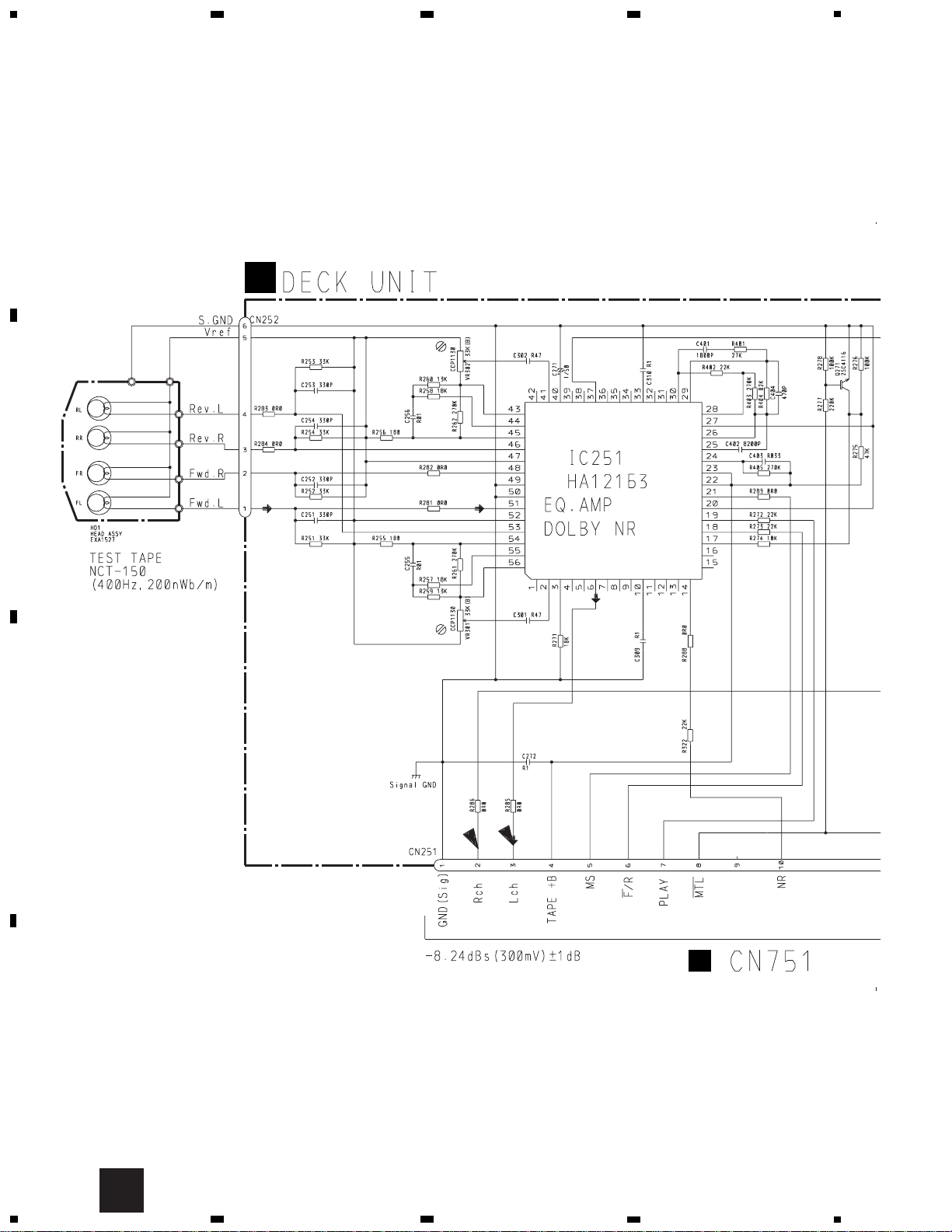
Unit Name : Deck Unit
MISCELLANEOUS
IC 251 IC HA12163
IC 351 IC PA2020A
Q 271 Transistor 2SC4116
Q 351 Transistor 2SB1260
Q 352 Transistor 2SC4102
D 351 Diode MA141K
VR 301 Semi-fixed 33kΩ(B) CCP1130
VR 302 Semi-fixed 33kΩ(B) CCP1130
RESISTORS
R 251 RS1/16S333J
R 252 RS1/16S333J
R 253 RS1/16S333J
R 254 RS1/16S333J
R 255 RS1/16S181J
R 256 RS1/16S181J
R 257 RS1/16S183J
R 258 RS1/16S183J
R 259 RS1/16S133J
R 260 RS1/16S133J
R 261 RS1/16S274J
R 262 RS1/16S274J
R 271 RS1/16S183J
R 272 RS1/8S223J
R 273 RS1/8S223J
R 274 RS1/8S103J
R 275 RS1/16S473J
R 276 RS1/16S104J
R 277 RS1/16S224J
R 278 RS1/16S104J
R 281 RS1/8S0R0J
R 282 RS1/8S0R0J
R 283 RS1/8S0R0J
R 284 RS1/8S0R0J
R 285 RS1/16S0R0J
R 286 RS1/16S0R0J
R 288 RS1/16S0R0J
R 289 RS1/16S0R0J
R 322 RS1/8S223J
R 351 RS1/16S102J
R 352 RS1/16S102J
R 353 RS1/16S102J
R 354 RS1/16S102J
R 355 RS1/10S274J
R 356 RS1/10S202J
R 357 RS1/10S472J
R 358 RS1/10S103J
R 359 RS1/10S103J
R 360 RS1/10S102J
R 361 RS1/10S622J
R 373 RS1/8S0R0J
R 374 RS1/8S0R0J
R 375 RS1/8S0R0J
R 401 RS1/16S273J
R 402 RS1/16S223J
R 403 RS1/16S274J
R 404 RS1/16S823J
R 405 RS1/16S274J
CAPACITORS
C 251 CKSRYB331K50
C 252 CKSRYB331K50
C 253 CKSRYB331K50
C 254 CKSRYB331K50
C 255 CKSRYB103K25
C 256 CKSRYB103K25
C 271 CEV1R0M50
C 272 CKSQYB104K16
C 301 CKSYB474K16
C 302 CKSYB474K16
56
KEH-P9700R,P9750
=====Circuit Symbol & No.===Part Name Part No.
--- ------ ------------------------------------------ -------------------------
=====Circuit Symbol & No.===Part Name Part No.
--- ------ ------------------------------------------ -------------------------
G
H
Page 57

57
KEH-P9700R,P9750
C 309 CKSQYB104K16
C 310 CKSQYB104K16
C 351 CKSYB224K25
C 352 CKSQYB392K50
C 353 CKSQYB103K50
C 354 CKSQYB103K50
C 355 CKSYB104K50
C 356 CKSQYB103K50
C 401 CKSRYB182K50
C 402 CKSRYB822K25
C 403 CKSRYB333K16
C 404 CKSRYB471K50
Unit Number :
Unit Name : PCB Unit
S 1 Switch (Load) ESG1004
S 2 Switch (70µS) ESG1004
EGN 1 Photo-Interrupter EGN1005
R 1 Resistor RD1/4PM181J
Unit Number :
Unit Name : Reel PCB
EGN 2 Photo-Interrupter EGN1006
EGN 3 Photo-Interrupter EGN1006
Unit Number :
Unit Name : Switch PCB
S 951 Switch CSN1012
S 952 Switch CSN1022
Miscellaneous Parts List
M 1 Motor Unit (Main) EXA1454
M 2 Motor Unit (Sub) EXA1485
HD 1 Head Assy EXA1527
M 951 Motor CXM1085
=====Circuit Symbol & No.===Part Name Part No.
--- ------ ------------------------------------------ -------------------------
I
J
K
Page 58

58
KEH-P9700R,P9750
VR501
DC V
Meter(2)
SIDE B
Q501 E
6. ADJUSTMENT
- Connection Diagram
TUNER AMP UNIT
BACK UP
ACC
GND
Lch +
Lch Rch +
Rch -
4Ω
4Ω
Mai n Antenna
Jack
+14.4V
GND
mV Meter (1)
Antenna Plug
Dummy Antenna
50Ω (37.5
Ω )
Ω(75Ω )
50
FM/AM TUNER UNIT (TOP VIEW)
L2
TC1
L4
T31
DC Regulated
Power Supply
Oscilloscope
FM SSG
Pin26
Pin 19
Pin14
Stereo
Modulator
DC V
Meter(1)
DECK UNIT
VR302
mV
Meter(2)
DECK UNIT
VR301
CN251
L-CH
Pin3
R-CH
FM/AM TUNER UNIT
Pin2
L5
Pin13
T51
VR154
Pin1
FM/AM TUNER UNIT (BOTTOM VIEW)
T51
C63
Center
Meter
Page 59

59
KEH-P9700R,P9750
Modulation M:MONO MOD., 400Hz 30%(22.5kHz Dev.)
S:STEREO MOD., 1kHz, L or R=30%(20.25kHz+7.5kHz Dev.)
NOTE:Before proceeding to further adjustments after switching power ON, let the tuner run for ten minutes to allow
the circuits to stabilize.
FM ADJUSTMENT(EW model)
FM SSG Displayed Adjustment Adjustment Method
No. Frequency(MHz) Level(dBf) Frequency(MHz) Point (Switch Position)
TUN Volt 1 ••••• ••••• 108.0 L5 DC V Meter(1) : 6V
IF 1 98.1 M 60 98.1 T51 Center Meter : 0
ANT Coil 1 98.1 M 5 98.1 L2 mV Meter(1) : Maximum
RF Coil 1 98.1 M 5 98.1 L4 mV Meter(1) : Maximum
Image 1 129.3 M 60—80 107.9 TC1 mV Meter(1) : Minimum
IFT 1 98.1 M 5 98.1 T31 mV Meter(1) : Maximum
(STEREO MODE)
ARC 1 98.1 S 39 98.1 VR154 mV Meter(1) : Separation 5dB
(STEREO MODE)
FM ADJUSTMENT(ES model)
FM SSG Displayed Adjustment Adjustment Method
No. Frequency(MHz) Level(dBf) Frequency(MHz) Point (Switch Position)
TUN Volt 1 ••••• ••••• 108.0 L5 DC V Meter(1) : 6V
IF 2 98.1 M 60 98.1 T51 Center Meter : 0
ANT Coil 3 98.1 M 5 98.1 L2 mV Meter(1) : Maximum
RF Coil 4 98.1 M 5 98.1 L4 mV Meter(1) : Maximum
IFT 5 98.1 M 5 98.1 T31 mV Meter(1) : Maximum
(STEREO MODE)
ARC 6 98.1 S 40 98.1 VR154 mV Meter(1) : Separation 5dB
(STEREO MODE)
RDS SL ADJUSTMENT
FM SSG Displayed Adjustment Adjustment Method
No. Frequency(MHz) Level(dBf) Frequency(MHz) Point (Switch Position)
1 106.1 M 52 106.1 VR501 DC V Meter(2) : 2.25V±0.05V
DOLBY B NR ADJUSTMENT
No. Test Tape Adjustment Point Adjustment Method
(Switch Position)
1 NCT-150 VR301(Lch),VR302(Rch) mV Meter(2) : –8.24dBs±1.0dB
(400Hz,200nwb/m) (DOLBY NR Switch : OFF)
Page 60

60
KEH-P9700R,P9750
7. GENERAL INFORMATION
7.1 PARTS
7.1.1 IC
VD
A
24
25
Bip
-
+
Z
ADD
SUB
(12)
I/O-3
910
I/O-2
FM
OUT
27
IN
H
S
+
N
C
AMT
V
30
-
+
Bip
12bit
A
M
IN
3233
+
34PD1
PD
REF
36
X-GND
XI
39
38
Z
(X-Y)
LDET
MODE
SW
(12)
P(12)
8bit
SHIFT
IF FM
7845
FM
VCO
AM
VCO
I/F
40
CE
41DI
42
CK
43
DO
2
NC
NC
1
(14)
37
XIO
SR
44
28
29
F
M
IN
11
DA(12)
DA
C
(12bit)
Vref
-
NC
23
+
VCO
SU
B
(14)
X
Y
CRESET
IN3 REG
(22bit)
A-GND
V
D
D
6
PD0
VREF
2
MO
S
Bi
p
I/O-1
V
REF2
V
REFP
17
18
IF
35
VREF
2
MO
S
OU
T
A
M
12
13
14
15
16
I/O-5
I/O-4
NC
O-7
O-6
CUR REQUEST
20
LDET
21
22
19
V
CC
OUT
1
SEL
OUT
2
SEL
IN1 REG
(31bit)
(16)
(4)
31
DIVIDER
4
BIT
SHIFT
42
11
12bit REG
PROGRAMABLE
DIVIDER
NC
COUNTER
3
D-
GND
NC
DATA REGISTER
26
IF AM
COUNTER
V
C
C
BAND
GA
P
FMTV
Bip
+
12bit SRx4
(12)
(12)
TVMEMORY
SEL
X
Y
PD & LDET
-
NC
14k
28k
35k
10k
UCOM
PM2007A
PM2007A
PD4903A
PD6237C
SED1540F0A
SED1526F0A
PD5445C
PM0017AM
AK4321VF
AK7712AVT
GGC1325(M5M51016BTP-70LL)
Page 61

61
KEH-P9700R,P9750
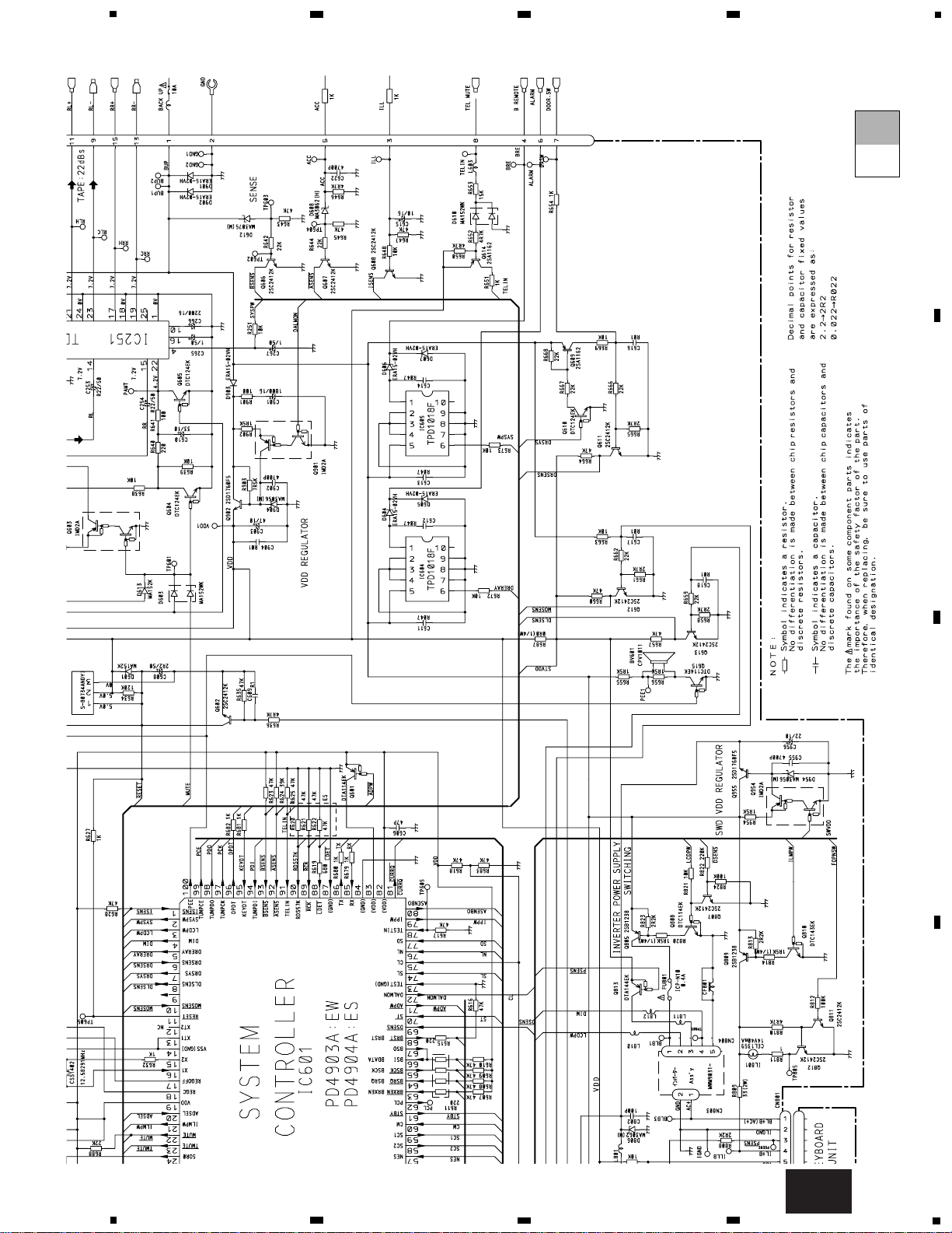
- Pin Functions (PD4903A)
Pin No. Pin Name I/O Function and Operation
1 isens I Illumination sense input
2 SYSPW O System power supply control output
3 LCDPW O CD power control
4 DIM O Dimmer select output
5 DRELAY O External relay output
6 DRSENS I Door open/close sense input
7 DRSYS O Door system select output
8 DLSENS I Door lock sense input
9 NC Not used
10 mosens I Motion/window damage sensor input
11 reset I Reset input
12 XT2 Not used
13 XT1 Connect to GND
14 VSS GND
15 X2 Crystal oscillator connection pin
16 X1 Crystal oscillator connection pin
17 REGOFF VDD
18 REGC VDD
19 VDD Power supply
20 ADSEL I Serial data audio source select input
21 ILMPW O Illumination power supply control output
22 mute O Mute output
23 tmute O Tuner mute output
24 SOR0 O Source select output
25 SOR1 O Source select output
26 SOR2 O Source select output
27 SOR3 O Source select output
28 FLPCLS O Flap motor close output
29 FLPOPN O Flap motor open output
30 fopnsw I Flap motor open switch input
31 fclssw I Flap motor close switch put
32 FLPPW O Flap motor driver power ON/OFF output
33 mcsens I Microphone sennse input
34 casens I Half load sense input
35 std/PRO I STD/PRO select input
36,37 NC Not used
38 dled O Alarm LED output
39 psense I Grille button sense input
40 VSS GND
41 VDD Power supply
42 SWVDD O Grille power supply control output
43 drst O Reset output
44 mdsens I Modulation detect input
45 sk I SK signal input
46 rdslk I RDS LK signal input
47 RDT I FROM data input
48 MSIN I MS sense
49 DIRO O Head F/R select output
50 PLAY O MS gain select output
51 mtlsw I Metal sense input
52 BC O Dolby B/C select output
53 NR O NR output
54 loadsw I Tape loading input
55 POS I Position sense input
56 RES I Reverse end sense input
57 NES I Forward end sense input
58 SC2 O Sub motor control output
Page 62

62
KEH-P9700R,P9750
Pin No. Pin Name I/O Function and Operation
59 SC1 O Sub motor control output
60 CM O Capstan motor control output
61 stby O Stand-by output
62 PCL O Clock adjustment output
63 brxen I/O P-BUS reception enable input/output
64 bsrq O P-BUS service request output pin
65 bsck I/O P-BUS serial clock input/output
66 BSI I P–BUS serial data input
67 BSO O P-BUS output
68 brst O P–BUS reset output
69 dsens I Grille detach sense
70 st I FM stereo input
71 adpw O Control output for analog input reference power
72 DALMON O DFS alarm output
73 TEST I Test terminal
74 SL I SD level input from tuner
75 CL I Synchronizing signal input of display data latch
76 NL I Noise level input
77 SD I SD input
78 TESTIN I Test program mode input
79 IPPW O Power supply control output for IP BUS interface IC
80 ASENBO O Slave power supply control output
81 currq O Tuner voltage FIX output
82,83 VDD Power supply
84 GND GND
85 RX I IP BUS data input
86 TX O Digital audio interface data output terminal
87 GND GND
88 ldet I PLL lock sense input
89 RCK I FROM clock input
90 RDS57K I 57kHzBP-OUT sense input
91 TELIN I Telephone mute input
92 asens I ACC power sense input
93 bsens I Back up power sense input
94 TUNPDI I PLL IC data input
95 KEYDT I Display data input
96 DPDT O Display data input
97 TUNPCK O PLL IC clock
98 TUNPDO O PLL IC data output
99 TUNPCE O PLL IC chip enable
100 PEE O Beep tone output
*PD4903A
IC's marked by* are MOS type.
Be careful in handling them because they are very
liable to be damaged by electrostatic induction.
51
75
50
76
26
100
25
1
Page 63

63
KEH-P9700R,P9750
- Pin Functions (PD6237C)
Pin No. Pin Name I/O Format Function and Operation
1-9 NC O C Not used
10 RDX O C Address read strobe output
11 VSS O C Digital GND
12 WRX O C Address write strobe output
13-18 NC O C Not used
19 KYDT O C Key data for system micro-computer
20 DPDT I Display data from system micro-computer
21 SCDCLK I Test program clock
22 DATAOT O C Test program data
23 Vcc Digital GND
24 DATAIN I Test program data
25,26 NC O C Not used
27 C C Reference voltage
28-33 NC O Not used
34 AVcc Analog power supply
35,36 NC Not used
37 AVSS Analog GND
38 ILM1 O C Illumination control output 1
39 ILM2 O C Illumination control output 2
40,41 NC O C Not used
42 GND Digital GND
43-48 NC O C Not used
49 MD0 I mode pin 0 (PULL-UP)
50 MD1 I mode pin 1 (PULL-UP)
51 MD2 I mode pin 2 (PULL-DOWN)
52 HSTX I Hardware standby input (PULL-UP)
53 REMIN I Remote control pulse input
54-58 NC O C Not used
59 KST0 O C Key scan output
60 KST1 O C Key scan output
61 KST2 O C Key scan output
62 KST3 O C Key scan output
63,64 NC O C Not used
65 RES1 O C SED 1450 Reset output
66 RES2 O C SED 1526 Reset output
67 KDT0 I C Key data input
68 KDT1 I C Key data input
69 KDT2 I C Key data input
70 KDT3 I C Key data input
71-73 NC O C Not used
74 OSC4K O C SED 1540 Clock output
75,76 NC O C Not used
77 NC I Not used
78 CS1 O C SED 1526 Chip select output
79 CS2 O C SED 1526 Chip select output
80 CS3 O C SED 1540 Chip select output
81 VSS Digital GND
82 X0 Oscillator circuit
83 X1 Oscillator circuit
84 Vcc Digital power supply
85 AD00 I/O C External data bus input/output
86 AD01 I/O C External data bus input/output
87 AD02 I/O C External data bus input/output
88 AD03 I/O C External data bus input/output
89 AD04 I/O C External data bus input/output
90 AD05 I/O C External data bus input/output
91 AD06 I/O C External data bus input/output
92 AD07 I/O C External data bus input/output
93 A0 O C External address output
94-100 NC O C Not used
Page 64

64
KEH-P9700R,P9750
*PD6237C
30
31
50
81
100
1
80
51
Format Meaning
C C MOS
SED1540F0A
- Pin Functions (SED1540F0A)
Pin No. Pin Name I/O Function and Operation
1-72 SEG71-0 O Output for driving segment of LC
73 A0 I Normally the lowest bit in the address bus of MPU is connected to distinguish
between data and command.
74,75 OSC1,2 Terminal to connect resistor for internal oscillation
76 E(rd) I Enable clock input terminal of 68-system MPU
Terminal to connect RD signal of 80-system MPU. While this signal is set to “L,”
data bus of SED1540 will be output.
77 R/w(wr) I Input terminal of read/write control signal
Terminal to connect write signal of 80-system MPU
78 VSS 0V connect to system GND
79-86 DB0-7 8-bit duplex data bus to be connected to a data bus of 8-bit or 16-bit standard MPU
87 VDD Connect to +5V power supply VDD
88 res Can be set to initial setting by setting RES to “L” when using 68-system MPU,
or by setting RES to “H” when using 80-system MPU.
89 FR I/O Input/output terminal of LC alternating signal
90 V3 Multilevel power supply for driving LC
91 cs I Chip select signal. Normally, signal obtained by decoding address bus signal is input.
92 NC Not used
93 M/S Terminal to select between master and slave operation to SED1540. Connect to
VDD or VSS.
94,95 V2,1 Multilevel power supply for driving LC
96-99 COM0-3 O Output for LC common (low) driving
100 SEG72 I/O Output for driving segment of LC
30
31
50
81
100
1
80
51
SED1526F0A
128
1
38
39
103
102
65
64
Page 65

65
KEH-P9700R,P9750
*PD5445C
20
21
40
41
60
80
1
61
Format Meaning
C C MOS
- Pin Functions (SED1526F0A)
Pin No. Pin Name I/O Function and Operation
1-5 V1-V5 Multilevel power supply for driving LCD
6 VR I Voltage adjustment
7 VDD +5V power supply
8 VOUT O Ascending voltage output
9 CAP2- O Ascending voltage capacitor connection
10 CAP2+ O Not used
11 CAP1- O Ascending voltage capacitor connection
12 CAP2+ O Ascending voltage capacitor connection
13 VSS GND
14 M/S I IC master/slave operation select
15 SR2 I MPU interface select, pararel/serial data inpur select and reset input
16 SR1 I MPU interface select, pararel/serial data inpur select and reset input
17 wr I MPU WR signal connection
18 rd I MPU RD signal connection
19 CS2 I Chip select signal
20 CS1 I Chip select signal
21 A0 I Data/command discrimination
22 FR O Not used
23 CL O Not used
24-31 D0-D7 I/O Serial data bus
32-39 COM0-7 O Output for LCD common driving
40-48 NC Not used
49-110 SEG0-61 O Output for driving segment of LCD
111-128 NC Not used
Page 66

66
KEH-P9700R,P9750
- Pin Functions (PD5445C)
Pin No. Pin Name I/O Format Function and Operation
1 SPCK I C Connect to GND
2 NC O C Not used
3 VST O C Electronic volume strobe output
4 VDT O C Electronic volume data output
5 VCK O C Electronic volume clock output
6 CNVss I Connect to Vss
7 MCKRQ I C CD unit MCK request input
8 NC O C Not used
9 reset I Micro-computer hard reset input
10 Xout O System clock output
11 Vss I GND
12 Xin I System clock input
13 Vcc I Micro-computer power supply 5V
14 nmi I C Connect to Vcc
15 BMUTEIN I C CD unit LR clock supply data
16 SPRQ I C Connect to GND
17 brst I C P-Bus reset input
18 ADTEST I C A.EQ test mode start
19 MICSNS I C A.EQ mic connection data
20 ADSEL O C Signal/select input of A.EQ mic
21 MUTERQ O C Hard mute output
22,23 NC O C Not used
24 DSPOUT O C DSP serial data output
25 DSPIN I C DSP serial data input
26 DSPCK O C DSP serial clock output
27 NC O C Not used
28 BSO O C P-BUS data output
29 BSI I C P-BUS data input
30 BSCK I/O C P-BUS serial clock input/output
31 NC O C Not used
32 bsrq I/O C Service request input
33 brxen I/O C Reception enable input
34,35 DSPERR1 I C Connect to GND
36 DZF1 I C Front digital 0 data input
37 DZF0 I C Rear digital 0 data input
38 DZF2 I C Sub woofer digital 0 data input
39 testin I C test program start/enable
40 DSPPW O C DSP power supply switching
41 NGO O C Noise gate ON/OFF
42-48 NC O C Not used
49 FMUTE O C Not used
50 SWMUTE O C Not used
51 VOICE I C Connect to GND
52-58 NC O C Not used
59 IFHIZ I C DSP micro-computer port Hi2 set (test mode port)
60 dsprst O C TC9331 hard reset
61 pd O C AK7712 power down
62 akrst O C AK7712 reset
63 dspcs@ O C AK7712 chip select
64 dspcs! O C TC9331 chip select
65 dsprq O C AK7712 data output request
66 DSPCd O C TC9331 command/data
67 DSPRDY I C AK7712 data ready
68 dspack I C DSP data write ready/ACK
69 SMODE O C Ak7712 master/slave
70 EMPIN I C CD unit emphasis data input
71 empout O C DAC emphasis output
72 LRCKK O C LRCK/BCLK select
Page 67

67
KEH-P9700R,P9750
Pin No. Pin Name I/O Format Function and Operation
73 SDATAK O C Audio data select:LRCKK inverted gate
74 NOISE I ASL noise input
75 AVss I Connect Vss
76 MCKOUT O C CD MCLK gate control
77 Vref I AD select reference voltage input
78 AVcc I Connect to Vcc
79 MO/ST I C Connect to GND
80 SPDT O C Not used
AK4321VF
- Pin Functions (PM0017AM)
Pin No. Pin Name Function and Operation
1 AGND Analog GND
2 Vref Reference voltage noise cut
3-8 IN1-6 CH1-6 input
9,10 NC Note used
11 Ct Terminal to set forced switching time
12 DGND Digital GND
13 STB Strobe input
14 CLK Clock input
15 DATA Data input
16 NC Not used
17-22 OUT6-1 CH6-1 output
23 DVCC Digital GND
24 AVCC Analog GND
PM0017AM
1
2
3
4
24
23
22
21
A GND
Vref
IN1
IN2
AVCC
5
6
7
8
20
19
18
17
IN3
IN4
IN5
IN6
9
10
11
12
16
15
14
13
NC
NC
Ct
D GND
NC
DVCC
OUT1
OUT2
OUT3
OUT4
OUT5
OUT6
DATA
CLK
STB
CKS
DVDD
DVSS
XTO XTI
PD
BICK
SDATA
DFS
DEM0
SMUTE
TTL
VREF BVDD
DIF0DZF
AVSS AVDD
VCOM
123456789101112
24
23 22 21 20 19 18 17 16 15 14 13
LRCK
DEM1
DIF1
AOUTL AOUTR
Clock OSC/Divider
Serial Input Interface De-emphasis Control
8x
Interpolator
CTF
SCF
8x
Interpolator
Modulator Modulator
CTF
SCF
Page 68

68
KEH-P9700R,P9750
- Pin Functions (AK7712AVT)
Pin No. Pin Name I/O Function and Operation
1 TSTI1 I Test input 1
2 OPCL I ADC,DAC connection select
3 pdad I AD reset control
4 pdda I DA reset control
5 pd I Power down
6 rst I Reset input
7 TSTIO1 I/O Test input/output 1
8 TSTIO2 I/O Test input/output 2
9 TSTIO3 I/O Test input/output 3
10,11 DVB Digital PCB power supply
12 SDIN2 I Serial data input 2
13 SDAD O Serial data output 2
14 SDOUT2 O Serial data output 3
15 SDDA I Serial data input 3
16 SDDA2 I Serial data input 4
17 SDOUT3 O Serial data output 4
18 SDOUT1 O Serial data output 1
19 SDIN1 I Serial data input 1
20 SMODE I Interface clock select
21 BCLK I/O Clock input/output for serial data input signal input/output
22 LRCK I/O L/R channel Identification Signal input/output
23 CLKO O Master clock output
24 DVDD Digital power supply
25 DVSS Digital GND
26 XTI I Clock input
27 XTO O Oscillator output
28 TSTI2 I CLKO output control
29 cs I Chip select input for micro-computer interface
30 wrq I Command register reset input for micro-computer interface
31 DVSS Digital GND
32 DVDD Digital power supply
33 SCLK I Serial data input clock input for micro-computer interface
34 SI I Serial data input for micro-computer interface
35 WRDY O Data write ready output for micro-computer interface
36 DRDY O Output data ready output for micro-computer interface
37 SO O Serial data output for micro-computer interface
38 casrf O External DRAM CAS/pseudo SRAM refresh
39 rasce O External DRAM RAS/pseudo SRAM-ce
40 we O External SRAM/pseudo SRAM/DRAM write signal output
41-48 A16-A9 O External RAM address output
49 DVSS Digital GND
50 DVDD Digital power supply
51-59 A8-A0 O External RAM address output
60 oe O External SRAM/pseudo SRAM/DRAM output enable signal output
61-68 IO0-IO7 I/O External RAM data input/output
69 DVSS Digital GND
70 DVDD Digital power supply
71 DZFSET I Zero position detect setup
72 DVSS Digital GND
73 DVDD Digital power supply
74,75 DVB Digital PCB power supply
76 DZF2 O Zero input detect (DAC2)
77 DZF1 O Zero input detect (DAC1)
78 NC Not used
79 AVB Analog PCB power supply
80 AOUTR2 O DAC2 Rch analog output 2
81 AOUTL2 O DAC2 Lch analog output 2
82 NC Not used
Page 69

69
KEH-P9700R,P9750
Pin No. Pin Name I/O Function and Operation
83 AOUTR1 O DAC1 Rch analog output 1
84 AOUTL1 O DAC1 Lch analog output 1
85 VRDAL I DAC reference voltage input
86 AVSS Analog GND
87 AVDD Analog power supply
88 VRDAH I DAC reference voltage input
89 NC Not used
90 AINR- I ADC Rch analog inverted input
91 AINR+ I ADC Rch analog input
92 AINL- I ADC Lch analog inverted input
93 AINL+ I ADC Lch analog input
94 VCOM O Common voltage
95 VRADL I ADC reference voltage input
96 AVSS Analog GND
97 AVDD Analog power supply
98 VRADH I ADC reference voltage input
99 AVB Analog PCB power supply
100 NC Not used
AK7712AVT
25
26
50
51
75
76
100
1
GGC1325(M5M51016BTP-70LL)
12345678910111213 14 15 16 17 18 19 20 21 22
44 43 42 41 40 39 38 37 36 35 34 33 32 31 30 29 28 27 26 25 24 23
A0-A15 : Address input
BC1,BC2 : Byte control input
CS : Chip select input
DQ1-DQ16 : Data input/output
GND : Ground
OE : Output enable input
VCC : Power supply
W : Write control input
NC
A12
A7
A6
A5
A4
A3
A2
A1
A0
CS
GND
OE
NC
DQ1
DQ2
DQ3
DQ4
DQ5
DQ6
DQ7
DQ8
NC
BC1
BC2
A14
A15
A13WA8
A9
A11
A10
GNDNCDQ16
DQ15
DQ14
DQ13
DQ12
DQ11
DQ10
DQ9
VCC
Page 70

70
KEH-P9700R,P9750
7.1.2 DISPLAY
- CAW1471
COMMON
SEGMENT
Page 71

71
KEH-P9700R,P9750
7.2 DIAGNOSIS
7.2.1 DISASSEMBLY
Cassette
Mechanism
Module
Connector
Mic PCB
B
B
C
A
A
A
Grille Assy
A
A
A
A
C
C
A
Note : Pull up and remove with Mic PCB.
(Be careful connecting for Connector.)
- Remove the Grille Assy
1. A × 4
2. Stopper × 2
3. Connector × 5
- Remove the Case (Not shown)
- Remove the Cassette Mechanism Module
1. A × 4
2. Connector × 1
A
- Remove the Tuner Amp Unit
1. A × 2
2. B × 2
3. C × 4
4. Stopper × 2
A
Connector
Connector
- Remove the DSP Unit
1. Stopper × 4
2. Connector × 1
3. Stopper × 2
Connector
C
Page 72

72
KEH-P9700R,P9750
MIC SENSE
18
M
M
M
MIC-L
TUN-L
TAPE-L
IP-BUS L
VDD
Q901
Q902
VDD REGULATOR
B.U
Q171
Q172
VDD
PROSTD
13
Q904
DSP+5V
REGULATOR
IC902
NJM78M05A
DSP+5V
B.U
Q903
SYSPW
12 3
82
83
531
X0
X1
RE
KEYBOARD PCB
E
SWITCH PCB
K
CN1901
S1902
RESET
S1901
P SENS
X1901
IC1901
RS-140
OPTICAL
INPUT
KEY
MATRIX
Q3
FM RF
ANT
T31
FM MIX
Q31 CF51
FM IF
FM
OSC
AM
OSC
FM / AM PROCESSOR
IC1 PA4023B
FM PROCESSOR
IC2 PA4024A
CF52
FM IF
CF53
FM IF
T51
41
6343532 36 16 18 23 25 31 30 28 33 40 7 43
19
20
14
20
18
L DET
7
9
18
19
25 29 9 4 5
37
1
2
3
12
6
7
15
16
3
1
8
14
12
6
7
15
16
3
1
8
14
6
7
11
1
5
8
11 6
B.U
B.U
5
14 3
12 3
1
34
29
28
30
31
80
8
10
85
86
23
74
77
87
43 44
39
12 3
2
2
1
2
1
2
1
5
2
1
51
53
56
Q271
PLAY
MTL
LOADMETAL
MODE
SENSE
MAIN
MOTOR
FWD SENSE
SUB
MOTOR
REV SENSE
2
1
4
5
17 19
22
CN251 CN751CN252
6
5
19 18 7 17
2
38 19
7
20 15 17 21 14 13 5 6 2
20
11 12
18
1
4
3
26 25
910 14 15 17 18 47 1 2
AM TV
Q201 Q202
FM +B AM +B TUN +B
FM +B
X401
7.2MHz
AM +B TUN
+B
AMRF / AGC
IC401
PM2007A
PLL
CF232
AM IF
GATE
DRIVER
FM SL
AM SL
FM IFC
AM IFC
VCO
FM SD
COMP
CN401
RX
TX
DRLK
MSENS
NOISE
A SENBO
SWDB
FMTV
XO
XI
LDET LDET
AMTV
AMIF
FMVCO
AMVCO
CN701
IP-BUS ISOLATOR
IP-BUS DRIVER
B.U
B.U
VREF
B.U
B.U
VCC
IP-BUS IN
MOTION
SENSE
DOOR
LOCK
Q701
Q702
Q301
CN601
CN301
CN302
MIC301
VR301 ASL AMP ASL FILTER
S601
VR501
Q501
Q407
Q403
Q406
SOURSE SELECTOR
SOURSE SELECTOR
Q405
CN101
X501
4.33MHz
RDS DECODER
RDS 57K DETECTOR
IC501
PMW001B
IC502
TA7S5393F
Q612
Q613
IC702
TA2050S
IC701
CA0008
BUS L+
BUS LBUS +
BUS -
32IC302
NJM2068M
51IC301
NJM2068M
ASL PCB
C
DECK UNIT
H
REEL UNIT
J
PCB UNIT
I
TUNER AMP UNIT
A
FM / AM TUNER UNIT
B
MOTOR
DRIVER
Q953
MOTOR DRIVE
REGULATOR
IC951
BA6288FS
Q952
Q951
S951 S952
AUTOMATIC
FLAP SENSE
CN952 CN951
AUTOMATIC
FLAP MOTOR
T MUTE
TUN L
LDET
SL
SD
RDS57K
15
DRST
13
MDSENS
IC102
BA3131FS
IC101
BA3131FS
Q351
Q352
IC351
PA2020A
IC251
HA12163
TAPE EQUALIZER
46 8
1098
1
1
32
46 8 1 3 2
SYSTEM CONT
IC601
PD4903
FLPPW
FCLSSW
TX
LDET
SD
SL
DRST
MDSENS
TMUTE
RX
MOSENS
DLSENS
ASENBO
FOPNSW
FLCLS
FLOPN
PSENS
UNBAL. /BAL.
27
IC103
NJM2100M
IP-BUSL
MIC JACK UNIT
G
2
4
4
1
TAPE L
MCSENS
CN4601
CN171
CN4602
MICS
DLED
38
DLED
72
DALMON
35
STD/PRO
CN703
CN702
FWD
LCH
REV
LCH
STBY
LOAD
CN253
20
4
3
20
4
3
CN801
FMIF
PEE
16
MIC PCB
D
7.3 EXPLANATION
7.3.1 BLOCK DIAGRAM
- KEH-P9700R/EW
Page 73

73
KEH-P9700R,P9750
5
1
ALARM
IC604
TPD1018F
B.U
6
Q607
9
10
5
6
1
2
FRONT Lch
OUT
REAR Lch
OUT
SUB WOOFER
OUT
B.U
CN201
Q203
Q603
Q207
Q211
2
4
6
17
FL IN
FL +
FL -
RL +
RL -
FL +
FL -
RL +
RL -
RL IN
STBYMUTE
3
21
23
5
14
12
12
10
11
9
CN251
POWER AMP
IC251
TDA7386
FRONT Lch
SPEALER
REAR Lch
SPEALER
FL
RL
SWL
DSPMUTE
22
4
SYSPW
11
3
54
7
9
2
Q604
AUDIO+8V
REGULATOR
IC901
PA2024A
AM +B
VDD
FM +B
TUN +B
B.U
BACK UP
Q605
SYSPW
Q606
Q608
BSENS
ASENS
ISENS
Q614
B.U
TELIN
5
1
B.REMOTE
IC605
TPD1018F
B.U
6
SYSPW
DRERAY
Q611
DRSENS
Q609
Q610
B.U
DRSYS
PEE
Q615
BUZZER DRIVE
BV601
DFS
ALARM
Q601
12
RESET
VDD
IC602
S-80730ANDYI
Q602
RESET
11
VDD
Q954
Q955
SWD VDD REGULATOR
B.U
B.U
B.U
Q809
Q810
Q813
Q807
Q805
Q808
BACK UP
ACC
B REMOTE
DOOR SW
ILL
TEL MUTE
1
5
3
8
4
6
7
ALARM
89
2
82
83
53
19
KYDT
X0
X1
REMIN
DPDT
20
S
LCD
CONTROL
IC1902
PD6237C
LCD DRIVE
LCD1901 EL1901
LCD DRIVE
LCD DRIVE
IC1903
SED1540FOA
IC1904
SED1526FOA
IC1905
SED1526FOA
INVERTER ASSY
8910
13
91
84
23
18
SDADSD
IN
12
11 11
13 13
74
19
9
40
10 12
76
21
18
5
8
18
1
2
4
2
4
6
17
5
3
22
20
18
21
S DATA
15
28
29
43 44 90
95 9620
89
2
1
CN101 CN3001
SWITCH
DSP UNIT
F
Q812
Q811
IC3141
BU4066BCFV
IC3101
AK7712AVT
IC3201
PE2001AF
SWITCH
DAC
IC3102
TC9331F
IC3103
GGC1325
(M5M51016BTP-70LL)
DSP SYSTEM
CONTROL
IC3001
PD5445A
AOUTL1
A OUT L
A OUT L1
MCK
MCK
SD OUT1
AINL-
AL-
NOISE
MCK OUT
SD OUT1
MIC SENS
RESET
DSPPW
MUTE
X3001
DSP
S-RAM
MCK
IC3142
TC7S08FU
IC3301
PM0017AM
CN3001
ELECTRONIC
VOLUME
IC601
PD4903A
DRST
MDSENS
RDS57K
KEYDT
DPDT
ILMPW
BSENS
93
ASENS
ISENS
TELIN
DRELAY
SYSPW
DRSENS
DRSYS
92
1
91
5
2
6
7
100
VDD
ADPW
71
83
15
28
29
33
MCSENS
15
16
X601
12.5879MHz
X2
X1
CN101
MUTE
22
SWVDD
42
12 32145
CN803 CN804
EL+B
IL GND
IL801
1
DSENS
69
DIM
4
LCDPW
3
Page 74

74
KEH-P9700R,P9750
8. OPERATIONS AND SPECIFICATIONS(ES model)
Connecting the Units
Green/red Gray/red
+
≠
Green
Green/black
Gray
Gray/black
+
≠
+
≠
Black/green Black/gray
+
≠
Multi-CD player
(sold separately)
Power amp
(sold separately)
Power amp
(sold separately)
Power amp
(sold separately)
Do not connect anything to the speaker
leads that are not connected to speakers.
Orange
Toterminal always supplied with power
regardless of ignition switch position.
Red
Toelectric terminal controlled by ignition
switch (12 V DC) ON/OFF.
Yellow
Tolight switch terminal.
Black (ground)
Tovehicle (metal) body.
Antenna jack
Brown
White
Yellow/black
If you use a cellular telephone, connect it via
the Audio Mute lead on the cellular telephone.
If not, keep the Audio Mute lead free of any
connections.
Fuse holder
Fuse resistor
Fuse resistor
Blue
Tosystem control terminal of the power
amp or Auto-antenna relay control
terminal.
(Max. 300 mA 12 V DC)
White/red
White/orange
See the section “DFS Alarm
Installation”.
White label (MID/FRONT OUTPUT)
Green label (HIGH/REAR OUTPUT)
Black label (LOW/SUBWOOFER OUTPUT)
IP-BUS cable
This Product
Small inverter unit
Connecting cords
with RCA pin plugs
(sold separately)
Left speaker
Use this for connections when
you have the separately
available amplifier.
Blue
PRO: Middle
STD: Front
Blue
Blue
Right speaker
PRO: High
STD: Rear
PRO: Low
STD: Subwoofer
Left speaker
PRO: Middle
STD: Front
Right speaker
PRO: High
STD: Rear
PRO:
When connecting to the speaker leads, do
not connect the RCA outputs.
When connecting to the RCA outputs, do
not connect the speaker leads.
Switch the PRO/STD Switch
PRO or STD.
(Refer to “The PRO/STD
Switch”.)
- Connection Diagram
Page 75

75
KEH-P9700R,P9750
Basic Operation
Switching Power ON/OFF
• Select the desired source (such as the tuner).
- Head Unit
Each press of the SOURCE/OFF button selects the desired source in the
following order:
CD player(one disc only) → Tuner →Tape →Multi-CD player→ AUX
To switch the sources OFF, hold down the SOURCE/OFF button for 1
second or more.
-
Remote Controller
Each press of the button selects the desired source in the following order:
TUNER button : Tuner →OFF
TAPE button : Tape → AUX → OFF
CD button : CD player (one disc only) → Multi-CD player→ OFF
Note:
• In the following cases, the sound source will not change:
* When a product is not connected to this unit.
* When no tape is set in this product.
* When no magazine is loaded in the Multi-CD player.
* When the AUX (external input) is set to OFF.
Key Finder
Head Unit
Remote Controller
Buttons 1—6
+/– button
DSP button
[/] button
BAND button
FUNCTION button
TUNER button
TAPEbutton
PGM button
ATT button
ANGLE button
CD button
DISPLAYbutton
▲/▼ button
BSM button
+/– button
S/A button PGM button 2/3 button
CLOCK button 5/∞ button
SOURCE/OFF button
OPEN/EJECT button
DISPLAYbutton
Page 76

76
KEH-P9700R,P9750
4. Raise or lower the volume.
5. Turn the source OFF.
Entering the Function Menu
In this menu you can select tuner functions.
• Select the desired mode in the Function Menu.
Each press of the FUNCTION button selects the mode in the
following order:
BSM → Local
To cancel the Function Menu, press the BANDbutton.
Note:
• After entering the Function Menu, if you do not perform an operation
within about 30 seconds, the Function Menu is automatically canceled.
Each press
changes the Mode ...
Hold for 1 second
Tuner Operation
Reset the AM tuning step from 9 kHz (the factory preset step) to 10
kHz when using the tuner in North, Central or South America.
Basic Operation of Tuner
1. Select Tuner.
2. Select the desired band.
3. Tune the receiver to a higher or lower frequency.
This product’s tuner lets you select the tuning by changing the
length of the time you press the button.
Manual Tuning (step by step) 0.3 seconds or less
Seek Tuning (automatically) 0.3–2 seconds
Manual Tuning (continuously) 2 seconds or more
Note:
• “STEREO ” indicator lights when a stereo station is selected.
• To select a weak broadcasting station that cannot be tuned in with the Seek
Tuning function, tune in with Manual Tuning.
“STEREO ”
FM1 → FM2 → FM3 → AM
Each press
changes the Source ...
Page 77

77
KEH-P9700R,P9750
Preset Tuning
Up to 18 FM stations (6 in FM1, FM2 and FM3) and 6 AM stations can
be stored in memory.
Store the stations in memory under buttons 1–6 beforehand with the
BSM (Best Stations Memory) or Preset Memory function.
BSM (Best Stations Memory)
The BSM function stores stations in memory automatically.
• Switch the BSM mode ON.
The stations with the strongest signals will be stored under buttons 1–6
and in order of their signal strength.
• To cancel the process, press the BSM button before
memorization is complete.
Note:
• You can also switch the BSM function ON/OFF in the Function Menu.
Hold for 2 seconds
Tuner Operation
Local Seek Tuning
This mode selects only stations with especially strong signals.
1. Select the Local mode (Local) in the Function
Menu.
2. Switch the Local mode ON or OFF.
3. Select the desired Local Seek sensitivity.
FM : Local 1 ↔ Local 2 ↔ Local 3 ↔ Local 4
AM : Local 1 ↔ Local 2
Note:
• The “Local 4” setting allows reception of only the strongest stations, while
lower settings let you receive progressively weaker stations.
To cancel the Function Menu, press the BANDbutton.
“LOC”
Page 78

78
KEH-P9700R,P9750
Using CD Player (one disc only)
This product can control a CD player (one disc only).
Basic Operation of CD Player
1. Select the CD player source.
Note:
• The CD player is selected only when a CD is loaded.
• If the CD player cannot operate properly, an error message such as “ERROR-
14” is displayed. Refer to the CD player owner’s manual.
2. Select the desired track (or fast-forward/reverse, per
the chart below).
This product lets you select the track search function or fast-
forward/reverse function by changing the length of the time you
press the button.
Track search 0.5 seconds or less
Fast-forward/Reverse Continue pressing
3. Raise or lower the volume.
4. Turn the source OFF.
Each press
changes the Source ...
Hold for 1 second
Each press
changes the Source ...
Each press
changes the Source ...
Using the Cassette Player
Basic Operation of Cassette Player
1. Open the front panel and insert the cassette tape.
“METAL” appears on the display for a few seconds when a metal or
chrome tape is inserted. Nothing is displayed for a normal tape.
2. Switch tape playback from side A to side B,or vice
versa.
3. Raise or lower the volume.
4. Remove the cassette tape.
Be sure to close the front panel by pressing the OPEN/EJECT
button after removing the cassette tape.
Note:
• The Tape function can only be turned ON/OFF with the cassette tape
remaining in this product.
Hold for 2 seconds
Page 79

79
KEH-P9700R,P9750
Music Group Playback
Only discs in the same group are played.
1. Select the Music Group Playback mode (Music Group)
in the Function Menu.
2. Select the desired Music Group.
Note:
• At first, the group of the disc playing is displayed. If the disc playing does not
belong to a group, “NO GROUP” is displayed.
3. Switch music group playback ON or OFF.
To cancel the Function Menu, press the BANDbutton.
Note:
• If there are no discs registered in the selected group, “MG EMPTY” is displayed.
Deleting a Disc from a Music Group
1. Play the disc you want to delete from a group.
2. Select the Music Group Input mode (MG Input) in the
Detailed Setting Menu.
3. Delete the disc from the group.
To cancel the Detailed Setting Menu, press the BANDbutton.
Note:
• During music group playback, if you have deleted the disc currently playing from
the group, the next disc in the group is played. If all discs in the same group have
been deleted, “NO GROUP” is displayed.
“Music G '”
Using Multi-CD Players
Music Group Play (for 50-Disc type only)
The Music Group Play function classifies discs loaded in a 50-Disc
type multi-CD player into 10 groups, and plays only discs from the
same group. Up to 100 discs can be classified into groups. (Music
Group, ITS program and Disc Title data for up to 100 discs can be
stored in memory.)
Note:
• Music Group types are as follows:
ROCK 1, ROCK 2, POP, JAZZ, INSTRMNT, CLASSIC, GROUP 1,
GROUP 2, GROUP 3, GROUP 4
Classifying a Disc into a Group
1. Play the disc you want to classify into a group.
2. Select the Music Group Input mode (MG Input) in
the Detailed Setting Menu.
3. Select the desired group.
4. Register the disc in the selected group.
To cancel the Detailed Setting Menu, press the BANDbutton.
Note:
• Even if you remove a disc from a magazine after you have registered it in
a group, its assigned group is stored in memory. This means that when you
reinsert the disc in the magazine, there’s no need to reassign it to the
group.
• After assigning 100 discs to groups, data input for a new disc overwrites
data for the disc that has been played least recently.
Page 80

80
KEH-P9700R,P9750
Entering the DSP Function Menu
In this menu you can select DSP Functions.
• Select the desired mode in the DSP Function Menu.
- PRO mode
Each press of the DSP button selects the mode in the following order:
Auto-equalizer mode (A.EQ Mode)* → Balance Adjustment mode
(Balance) → Graphic Equalizer mode (EQ-Nuance) → 13-Band
Graphic Equalizer Adjustment mode (EQ-Fine)** → Position Selector
mode (Position)
* If Auto-equalizing is not performed, you cannot switch to the Auto-equalizer
mode.
** You can switch to the 13-Band Graphic Equalizer Adjustment mode only when
selecting a user curve in the Graphic Equalizer mode.
To cancel the DSP Function Menu, press the BAND button.
Note:
• After entering the DSP Function Menu, if you do not perform an operation
within about 30 seconds, the DSP Function Menu is automatically canceled.
- STD mode
Each press of the DSP button selects the mode in the following order:
Auto-equalizer mode (A.EQ Mode)* → Balance Adjustment mode
(Fader) → Graphic Equalizer mode (EQ-Nuance) → 13-Band Graphic
Equalizer Adjustment mode (EQ-Fine)** → Sound Field Control (SFC
Mode) → Position Selector mode (Position)
* If Auto-equalizing is not performed, you cannot switch to the Auto-equalizer
mode.
** You can switch to the 13-Band Graphic Equalizer Adjustment mode only when
selecting a user curve in the Graphic Equalizer mode.
To cancel the DSP Function Menu, press the BAND button.
Note:
• After entering the DSP Function Menu, if you do not perform an operation
within about 30 seconds, the DSP Function Menu is automatically canceled.
Each press
changes the Mode ...
Using the Digital Signal Processor (DSP)
Switching the Operation Mode
• Set the PRO/STD switch to PRO or STD.
Set the PRO/STD switch on the side of the unit to the desired
Operation mode with a pen tip or other pointed instrument. After
switching, reset the unit.
Note:
• If you press the RESET button, information in the unit’s Preset memory
and other information is erased.
Page 81

81
KEH-P9700R,P9750
Position Selector Function
One way to assure a more natural sound is to clearly position the
stereo sound image (putting you in the center of the sound field).
The Position Selector function adjusts delay time and volume level
of sound from each speaker to match seat positions and the number
of people in the car, and lets you recall settings at the touch of a
button. The result is a natural sound regardless of the seat you are
sitting in.
Button Position
' Front seat
' Front and Rear seat
[ Driver’s seat (steering located on the LEFT side)
] Driver’s seat (steering located on the RIGHT side)
Note:
• In the PRO mode, front and rear seats cannot be selected.
About the Position Indicator
This lets you confirm current Position setting without switching to
the Position Selector mode.
Front-Left Front-Right Front All
Setting the Listening Position
1. Select the Position Selector mode (Position) in the
DSP Function Menu.
2. Press one of buttons
'/'/[/] to select the
desired Position. (e.g. Press button
[.)
To cancel the listening position, press the same button again.
Note:
• In the PRO mode, pressing the ' button cancels the listening position.
Using the Digital Signal Processor (DSP)
Entering the DSP Detailed Setting Menu
In this Menu, you can select functions enabling adjustment of
settings to match conditions in your car, such as the Network mode
and Automatic Sound Levelizer.
• Enter the DSP Detailed Setting Menu.
- PRO mode
Each press of the DSP button selects the mode in the following
order:
Network mode (Low-NW) → Time Alignment mode (T.Alignment)
→ Loudness mode (Loudness) → Automatic Sound Levelizer
mode (ASL) → Source Level Adjustment mode (SLA)*
* When the source is an FM broadcast, you cannot switch to the Source
Level Adjustment mode (SLA).
To cancel the DSP Detailed Setting Menu, press the BAND button.
Note:
• After entering the DSP Detailed Setting Menu, if you do not perform an
operation within about 30 seconds, the DSP Detailed Setting Menu is
automatically canceled.
- STD mode
Each press of the DSP button selects the mode in the following
order:
Network mode (Sub-W-NW) →Loudness mode (Loudness) →
Automatic Sound Levelizer mode (ASL) → Source Level
Adjustment mode (SLA)*
* When the source is an FM broadcast, you cannot switch to the Source
Level Adjustment mode (SLA).
To cancel the DSP Detailed Setting Menu, press the BAND button.
Note:
• After entering the DSP Detailed Setting Menu, if you do not perform an
operation within about 30 seconds, the DSP Detailed Setting Menu is
automatically canceled.
Hold for 2 seconds
Page 82

KEH-P9700R,P9750
DSP
Equalizer (13 Band Graphic Equalizer)
Frequency...............50, 80, 125, 200, 315, 500, 800,
1.25 k, 2 k, 3.15 k, 5 k, 8 k, 12.5 k (Hz)
Level ............................................... ± 12 dB (2 dB)
Auto Equalizer (STD Mode)
(Front & Rear & Subwoofer 13 band graphic +
Rear 2 band parametric)
Frequency (Front & Rear & Subwoofer)
............................ 50, 80, 125, 200, 315, 500, 800,
1.25 k, 2 k, 3.15 k, 5 k, 8 k, 12.5 k (Hz)
Frequency (Rear) ............ 100 Hz – 8 kHz (1/3 oct)
Level ...................................... +6 — –12 dB (2 dB)
Q Factor (Rear) .......................................... 1.2, 3.6
Auto Equalizer (PRO Mode)
(13 band graphic)
Frequency ............ 50, 80, 125, 200, 315, 500, 800,
1.25 k, 2 k, 3.15 k, 5 k, 8 k, 12.5 k (Hz)
Level ...................................... +6 — –12 dB (2 dB)
Network (STD Mode)
Front/Rear HPF frequency: 50, 80, 125, 200 (Hz)
Slope: 0, –6, –12 dB/oct
Level: 0 — –24 dB (1 dB)
Subwoofer (Mono)
............................ LPF frequency: 50, 63, 80, 100,
125, 160, 200 (Hz)
Slope: –6, –12, –18 dB/oct
Level: +6 — –24 dB (1 dB)
Phase: Normal/Reverse
Network (PRO Mode)
High .. HPF frequency: 2 k, 2.5 k, 3.15 k, 4 k, 5 k,
6.3 k, 8 k, 10 k, 12.5 k (Hz)
Slope: –6, –12, –18, –24 dB/oct
Level: +6 — –24 dB (1 dB)
Phase: Normal/Reverse
Mid .... LPF frequency: 2 k, 2.5 k, 3.15 k, 4 k, 5 k,
6.3 k, 8 k, 10 k, 12.5 k (Hz)
HPF frequency: 40, 50, 63, 80, 100, 125,
160, 200, 250 (Hz)
Slope: 0, –6, –12, –18, –24 dB/oct
Level: 0 — –24 dB (1 dB)
Phase: Normal/Reverse
Low (Stereo/Mono)
...................... LPF frequency: 40, 50, 63, 80, 100,
125, 160, 200, 250 (Hz)
Slope: –12, –18, –24, –30, –36 dB/oct
Level: +6 — –24 dB (1 dB)
Phase: Normal/Reverse
Time Alignment ....................... 0 — 400 cm (2 cm)
0 — 160 inch (0.5 inch)
Note:
• Specifications and the design are subject to
possible modification without notice due to
improvements.
Specifications
General
Power source ...... 14.4 V DC (10.8 – 15.1 V allowable)
Grounding system .................................... Negative type
Max. current consumption......................................... 10 A
Dimensions
(DIN) (chassis) ....178 (W) × 50 (H) × 155 (D) mm
(nose) ....... 188 (W) × 58 (H) × 20 (D) mm
(D) (chassis) ... 178 (W) × 50 (H) × 160 (D) mm
(nose) ......... 170 (W) × 46 (H) × 15 (D) mm
Weight ..................................................................... 1.8 kg
Amplifier (KEH-P9700R/EW)
Maximum power output .................................... 40 W × 4
Continuous power ourput ................................. 25 W × 4
(DΙΝ45324, +Β =14.4 V)
Load impedance ....................... 4 Ω (4 – 8 Ω allowable)
Preout output level/output impedance ..... 500 mV/1 kΩ
Amplifier (KEH-P9750/ES)
Continuous power output is 20 W per channel
min. into 4 ohms, both channels driven 50 to
15,000 Hz with no more than 5% THD.
Maximum power output ................................... 40 W × 4
Load impedance ........................ 4 Ω (4 – 8 Ω allowable)
Preout output level/output impedance ...... 500 mV/1 kΩ
Cassette player
Tape .......................Compact cassette tape (C-30 – C-90)
Tape speed .... 4.76 cm/sec.(+0.14cm/sec.,-0.05cm/sec.)
Fast forward/rewinding time Approx. 100 sec. for C-60
Wow & flutter ........................................ 0.09% (WRMS)
Frequency response........ Metal: 30 – 22,000 Hz (±3 dB)
Stereo separation .................................................... 45 dB
Signal-to-noise ratio
.... Metal: Dolby B NR IN: 67 dB (IEC-A network)
Dolby NR OUT: 61 dB (IEC-A network)
FM tuner
Frequency range .................................... 87.5 – 108 MHz
Usable sensitivity
............... 11 dBf (1.0 µV/75 Ω, mono, S/N: 30 dB)
50 dB quieting sensitivity .. 16 dBf (1.7 µV/75 Ω, mono)
Signal-to-noise ratio .................... 70 dB (IEC-A network)
Distortion ........................ 0.3% (at 65 dBf, 1 kHz, stereo)
Frequency response .................... 30 – 15,000 Hz (±3 dB)
Stereo separation ...................... 40 dB (at 65 dBf, 1 kHz)
AM tuner (KEH-P9750/ES)
Frequency range ....................... 531 – 1,602 kHz (9 kHz)
530 – 1,710 kHz (10 kHz)
Usable sensitivity ............................ 18 µV (S/N: 20 dB)
Selectivity ................................................ 50 dB (±9 kHz)
50 dB (±10 kHz)
MW tuner (KEH-P9700R/EW)
Frequency range .................................... 531 – 1,602 kHz
Usable sensitivity ............................ 18 µV (S/N: 20 dB)
Selectivity ............................................... 50 dB (±9 kHz)
LW tuner (KEH-P9700R/EW)
Frequency range ....................................... 153 – 281 kHz
Usable sensitivity ............................ 30 µV (S/N: 20 dB)
Selectivity ............................ .................. 50 dB (±9 kHz)
 Loading...