

Page 1

• HTV-SW1
ORDER NO.
SURROUND MODE
STANDBY/ON
• HTV-C1
DISPLAY INPUT
VOLUME
RRV2060
POWERED SUBWOOFER
HTV-SW1
CONTROL CENTER
HTV-C1
THIS MANUAL IS APPLICABLE TO THE FOLLOWING MODEL(S) AND TYPE(S).
Type Power Requirement
Model
HTV-SW1 HTV-C1
DDXJ ‡ AC110–127V/220–230V/240V With the voltage selector
The voltage can be converted by
the following method.
ADXJ ‡ AC power supplied from power trans-
This product is a system component. This product does not function properly when independent;
to avoid malfunctions, be sure to connect it to the prescribed system component, otherwise
damage may result. The Powered Subwoofer HTV-SW1 is a part of the Hometheater System HTV-
1.
Hometheater System Control Center
HTV-1 HTV-C1 (this service manual)
(service manual RRV2063)
CONTENTS
1. SAFETY INFORMATION....................................2
2. EXPLODED VIEWS AND PARTS LIST .............3
3. SCHEMATIC DIAGRAM................................... 10
4. PCB CONNECTION DIAGRAM .......................24
5. PCB PARTS LIST.............................................36
6. ADJUSTMENT.................................................. 39
7.GENERAL INFORMATION ............................... 40
7.1 PARTS........................................................40
former's secondary of other system component
Powered Subwoofer
HTV-SW1 (this service manual)
Power Amp
HTV-A1 (this service manual)
7.1.1 IC ...........................................................40
7.1.2 DISPLAY................................................42
7.2 DIAGNOSIS................................................43
7.3 TEST MODE(HTV-C1) ...............................45
7.4 INDEPENDENT OPERATION DIAGNOSIS46
7.5 BACKUP FUNCTION (HTV-C1)................. 47
7.6 BLOCK DIAGRAM...................................... 48
8.PANEL FACILITIES AND SPECIFICATIONS..... 50
PIONEER ELECTRONIC CORPORATION 4-1, Meguro 1-Chome, Meguro-ku, Tokyo 153-8654, Japan
PIONEER ELECTRONICS SERVICE, INC. P.O. Box 1760, Long Beach, CA 90801-1760, U.S.A.
PIONEER ELECTRONIC (EUROPE) N.V. Haven 1087, Keetberglaan 1, 9120 Melsele, Belgium
PIONEER ELECTRONICS ASIACENTRE PTE. LTD. 253 Alexandra Road, #04-01, Singapore 159936
PIONEER ELECTRONIC CORPORATION 1998
T–ZZR NOV. 1998 Printed in Japan
Page 2
HTV-SW1, HTV-C1
1. SAFETY INFORMATION
This service manual is intended for qualified service technicians; it is not meant for the casual
do-it-yourselfer. Qualified technicians have the necessary test equipment and tools, and have been
trained to properly and safely repair complex products such as those covered by this manual.
Improperly performed repairs can adversely affect the safety and reliability of the product and may
void the warranty. If you are not qualified to perform the repair of this product properly and safely, you
should not risk trying to do so and refer the repair to a qualified service technician.
WARNING
This product contains lead in solder and certain electrical parts contain chemicals which are known to the state of California to
cause cancer, birth defects or other reproductive harm.
Health & Safety Code Section 25249.6 – Proposition 65
NOTICE
(FOR CANADIAN MODEL ONLY)
Fuse symbols (fast operating fuse) and/or (slow operating fuse) on PCB indicate that replacement parts
must be of identical designation.
REMARQUE
(POUR MODÈLE CANADIEN SEULEMENT)
Les symboles de fusible (fusible de type rapide) et/ou (fusible de type lent) sur CCI indiquent que les
pièces de remplacement doivent avoir la même désignation.
(FOR USA MODEL ONLY)
1. SAFETY PRECAUTIONS
The following check should be performed for the
continued protection of the customer and service
technician.
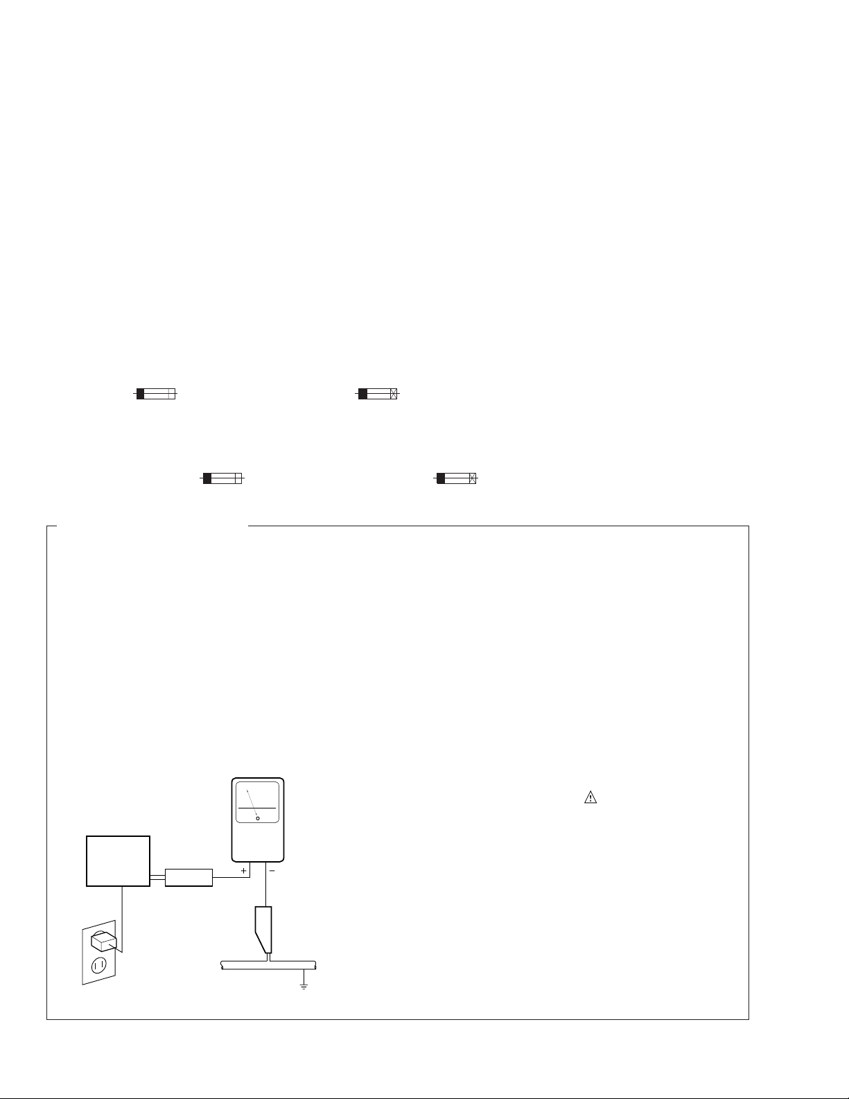
LEAKAGE CURRENT CHECK
Measure leakage current to a known earth ground
(water pipe, conduit, etc.) by connecting a leakage
current tester such as Simpson Model 229-2 or
equivalent between the earth ground and all exposed
metal parts of the appliance (input/output terminals,
screwheads, metal overlays, control shaft, etc.). Plug
the AC line cord of the appliance directly into a 120V
AC 60 Hz outlet and turn the AC power switch on. Any
current measured must not exceed 0.5 mA.
Reading should
not be above
0.5 mA
Earth ground
Device
under
test
Also test with plug
reversed
(Using AC adapter
plug as required)
Leakage
current
tester
Test all exposed
metal surfaces
AC Leakage Test
ANY MEASUREMENTS NOT WITHIN THE LIMITS
OUTLINED ABOVE ARE INDICATIVE OF A POTENTIAL SHOCK HAZARD AND MUST BE CORRECTED BEFORE RETURNING THE APPLIANCE
TO THE CUSTOMER.
2. PRODUCT SAFETY NOTICE
Many electrical and mechanical parts in the appliance have special safety related characteristics. These
are often not evident from visual inspection nor the
protection afforded by them necessarily can be obtained by using replacement components rated for
voltage, wattage , etc. Replacement parts which have
these special safety characteristics are identified in
this Service Manual.
Electrical components having such features are
identified by marking with a
on the parts list in this Service Manual.
The use of a substitute replacement component which
does not have the same safety characteristics as the
PIONEER recommended replacement one, shown in
the parts list in this Service Manual, may create shock,
fire, or other hazards.
Product Safety is continuously under review and
new instructions are issued from time to time. For
the latest information, always consult the current
PIONEER Service Manual. A subscription to, or additional copies of, PIONEER Service Manual may be
obtained at a nominal charge from PIONEER.
on the schematics and
2
Page 3
HTV-SW1, HTV-C1
2. EXPLODED VIEWS AND PARTS LIST
NOTES : ÷ Parts marked by “ NSP ” are generally unavailable because they are not in our Master Spare Parts List.
÷ The
÷ Screw adjacent to
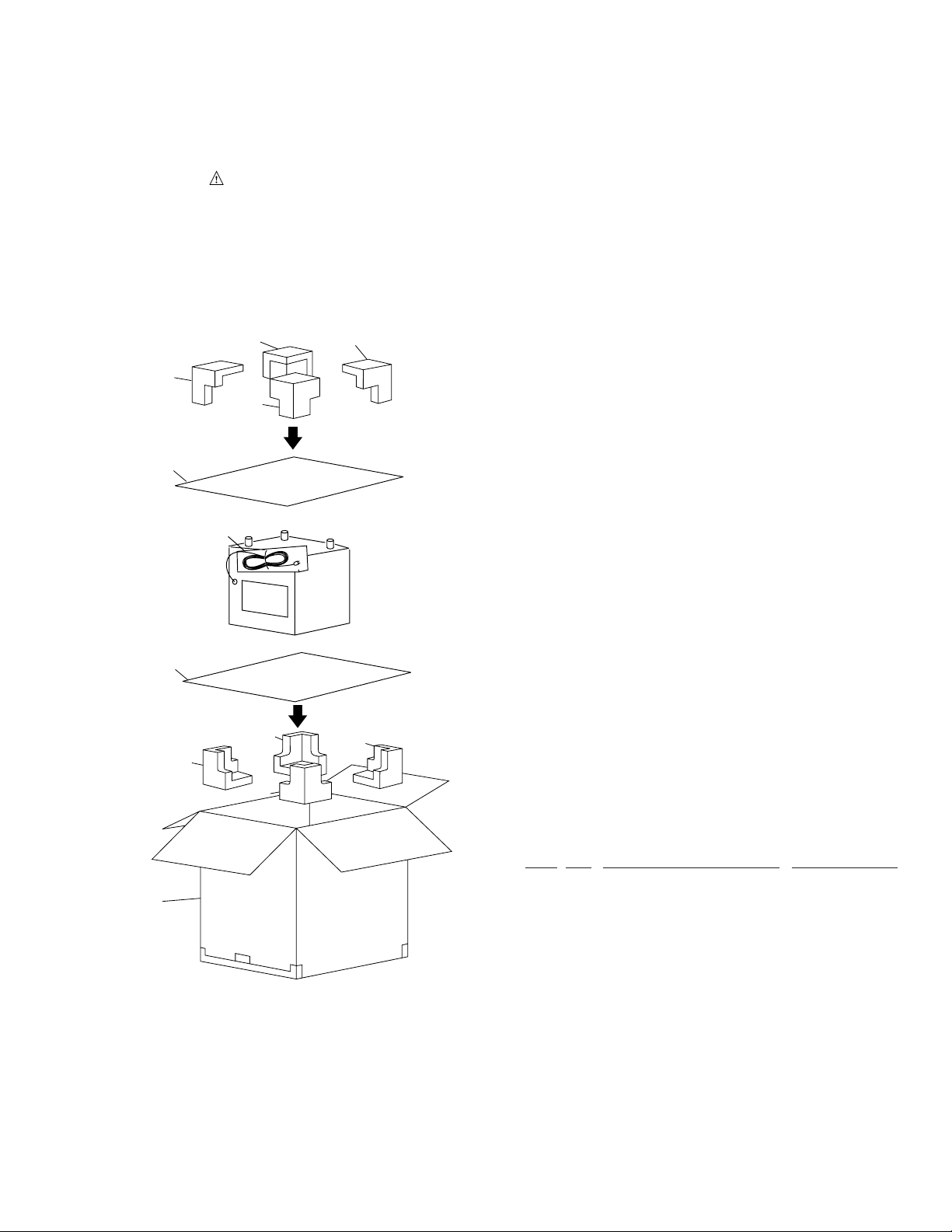
2.2 HTV-SW1
2.1.1 PACKING
mark found on some component parts indicates the importance of the safety factor of the part.
Therefore, when replacing, be sure to use parts of identical designation.
mark on the product are used for disassembly.
∞
1(1/4)
2(1/4)
1(3/4)
1(2/4)
4
1(4/4)
6
Rear
3
2(3/4)
2(2/4)
2(4/4)
÷ PACKING PARTS LIST(HTV-SW1)
Mark No. Description Part No.
1 Protector Top SHA2140
5
NSP 6 Polyethylene Bag SHL1227
2 Protector Bottom SHA2141
3 Protection Sheet S6 SHC1726
4 Protection Sheet S7 SHC1727
5 Packing Case SHG2124
(0.03 × 115 × 270)
3
Page 4

HTV-SW1, HTV-C1
2.1.2 EXTERIOR ( Cabinet HTV-SW1 )
2
6
8
10
1
4
5
A
9
3
7
A
5
9
8
A
8
Refer to "2.1.3 POWER AMP SECTION"
÷ EXTERIOR(Cabinet HTV-SW1) PARTS
8
LIST
8
Mark No. Description Part No.
NSP 1 Cabinet SMM1821
NSP 2 Power AMP HTV-A1/DDXJ
3 Connecting Cord SDF1072
NSP 4 Paper Port tube SMR1283
5 Foot SNK2274
NSP 6 CAUTION LABEL SRR1012
NSP 10 Logo 40 SAM1452
4
7 Speaker Q20EU82-52F
8 Screw BYC40P200FZB
9 Bind Tapping Screw BYC40P300FZK
Page 5
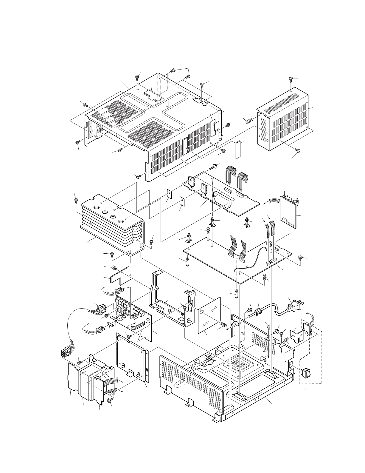
2.1.3 EXTERIOR ( POWER AMP HTV-A1)
HTV-SW1, HTV-C1
23
23
23
11
27
28
23
29
23
18
15
16
23
23
29
23
33
23
21
2
18
15
23
29
30
22
18
17
F
D
C
29
23
31
23
B
A
5
24
1
9
23
19
32
23
16
23
G
20
23
G
12
29
22
23
E
8
7
23
F
29
25
E
13
23
22
A
B
D
C
3
6
22
4
14
10
26
5
Page 6

HTV-SW1, HTV-C1
EXTERIOR(POWER AMP HTV-A1) PARTS LIST
•
Mark No. Description Part No.
1 AFPS ASSY AWU7262
2 PAMP ASSY AWU7263
3 PT PRI ASSY AWU7264
4 PT SEC ASSY AWU7265
5 JACK ASSY AWU7257
6 Power Transformer (T1) ATS7228
7 Fuse (FU1 : T3.15AL250V) REK1027
8 Fuse (FU2, 3 : T1.6AL250V) REK1024
9 AC Power Cord VDG1058
NSP 10 Chassis ANA7093
NSP 11 Heat Sink ANH7079
NSP 18 PCB Holder PNW2174
27 Connector Assy 6P ADX7245
NSP 28 Cord Support Assy • • • • •
NSP 32 Volt Selector Label AAX7667
NSP 33 POWER SW Label AAX7669
12 PW Barrier AEC7157
13 ST Barrier AEC7155
14 TRANS Frame ANG7216
15 Mini Card Spacer AEC7143
16 Mica Sheet AEE7010
17 Strain Relief CM-22B
19 Bonnet Case AZN7214
20 PCB Stay ANG7217
21 Screw ABA-258
22 Screw ASZ40P060FMC
23 Screw BBZ30P080FMC
24 Screw IBZ30P080FMC
25 STANDBY PT Assy AWU7267
26 PW SWITCH Assy AWU7259
29 Push Rivet AEC7149
30 Cushion AEB7123
31 Heat Protector AEC7136
6
Page 7

2.2 HTV-C1
2.2.1 PACKING
HTV-SW1, HTV-C1
5
15
12
13
15
2
3
14
2
4
9
11
18
6
7
23
20
16
19
PACKING PARTS LIST
•
17
Mark No. Description Part No. Mark No. Description Part No.
NSP 1 MOUNT ASSY AEA7021
2 Bolt Cap AEB7111
3 Velcro Hook(BLACK) AED7028
4 Velcro Loop(BLACK) AED7029
5 Operating Instructions ARE7183
(English/Spanish/Portuguese
/Chinese)
6 8P DIN Cable ADE7023
NSP 7 Speaker Cable 6P ADX7239
8 • • • • •
9 Remote Control Unit AXD7186
(CU-HT007)
10 • • • • •
11 Battery Cover RZN1156
12 Output Cable (L = 1.5m) VDE1052
NSP 13 Batteris(R06P,AA) VEM-013
NSP 14 Polyethylene Bag Z21-033
15 Polyethylene Bag Z21-038
(0.03 × 230 × 340)
16 L Protector AHA7209
17 R Protector AHA7210
18 Paper Protector AHA7217
19 Packing Case AHD7646
20 Packing Sheet AHG7053
21 Bolt(M6X140) ABA7042
22 Bolt(M6X90) ABA7041
23 Nut NA60FZK
24 Wing Nut NR60FZK
25 Washer WB60FZK
21
22
24
1
25
7
Page 8
HTV-SW1, HTV-C1
2.2.2 MAIN SECTION
15
22
19
16
A
5
22
25
22
2
1
23
4
13
16
22
9
22
8
3
22
22
7
18
23
23
22
23
22
21
14
24
Slit
(BOTTOM VIEW)
24
A
12
20
11
6
24
17
10
20
12
10
A
11
Slit
24
CAUTION :
Insert a screwdriver into the slit under the Grille Assy to pry open
the grille assy gradually and uniformly.
6
8
Page 9

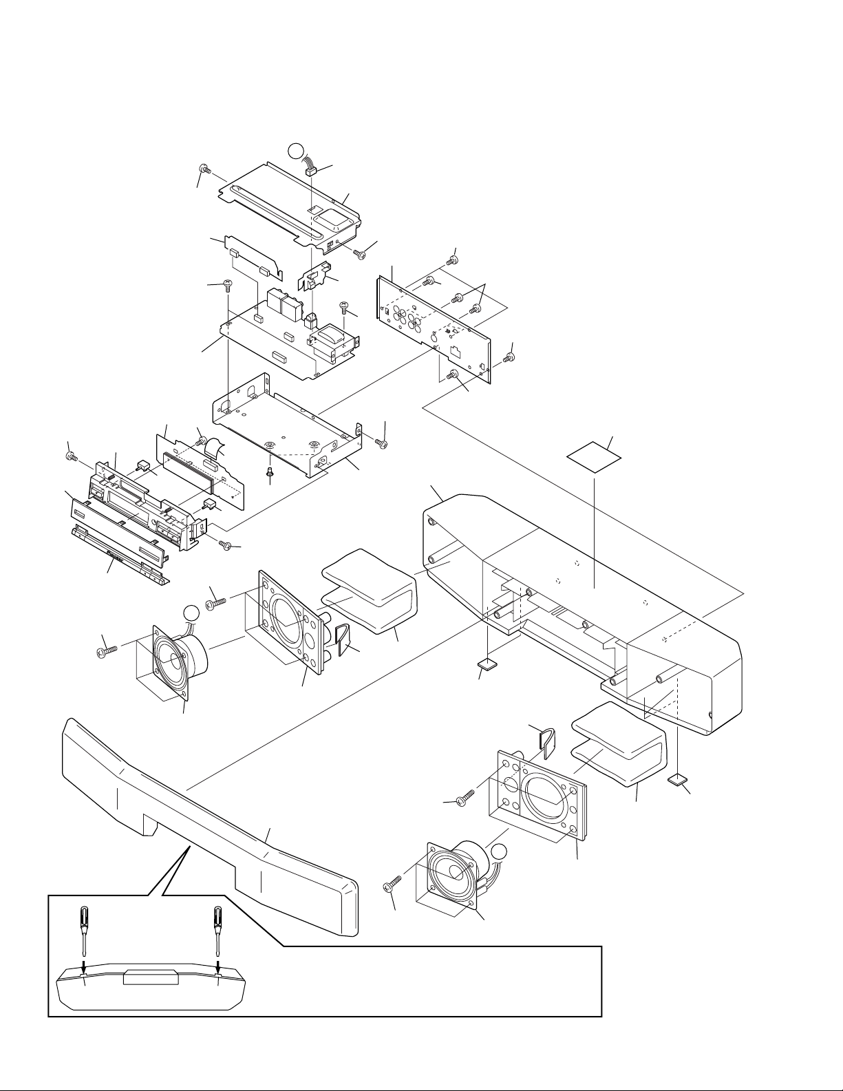
MAIN SECTION PARTS LIST
•
Mark No. Description Part No.
1 DISPLAY Assy AWU7260
2 MAIN Assy AWU7261
3 TERMINAL Assy AWU7251
4 21P FFC/30V ADD7124
5 Cable Assy 4P ADX7240
HTV-SW1, HTV-C1
Mark No. Description Part No.
16 Lens AAK7551
17 Grille Assy AAS7001
NSP 18 Rear Case AMC7028
19 Sub Panel AMD7003
20 Acoustic Shield AEB7130
NSP 7 PCB Bracket ANA7068
6 Speaker D87DU61-51F
8 Rear Panel ANC7716
NSP 9 Shield Cover ANK7040
10 Cushion 3 AEB7110
NSP 11 Baffle AMD7006
NSP 12 Acoustic Absorbent AMT7001
13 Card Spacer DNK2769
14 Button AAD7498
15 Display Panel AAK7595
NSP 21 Founding Caution AAX7660
22 Screw BBZ30P080FMC
23 Screw VPZ30P080FMC
24 Screw BPZ40P140FZK
25 INPUT LEV. Assy AWU7252
9
Page 10

1
HTV-SW1, HTV-C1
3. SCHEMATIC DIAGRAM
3.1 HTV-A1
3.1.1 OVERALL CONNECTIONS
A
B
23
PAMP ASSY
F
(AWU7263)
4
C
D
FROM
CONTROL
CENTER
(HTV–C1)
H
JA4001
TO
CONTROL
CENTER
(HTV–C1)
G
JACK ASSY
(AWU7257)
AFPS ASSY
A
(AWU7262)
10
H
CN501
1234
Page 11
5
678
HTV-SW1, HTV-C1
Note : When ordering service parts, be sure to refer to "EXPLODED VIEWS and P AR TS LIST" or "PCB PARTS LIST".
PW
E
SWITCH
ASSY
(AWU7259)
AC110 -127V
220-230V/240V
50/60Hz
!
AC POWER CORD
VDG1058
A
B
PT SEC
ASSY
(AWU7265)
STANDBY
D
PT ASSY
(AWU7267)
B
AKP7038
AKP7038
C
C
PT PRI
ASSY
!
T1 : ATS7228
5
6
7
(AWU7264)
11
8
D
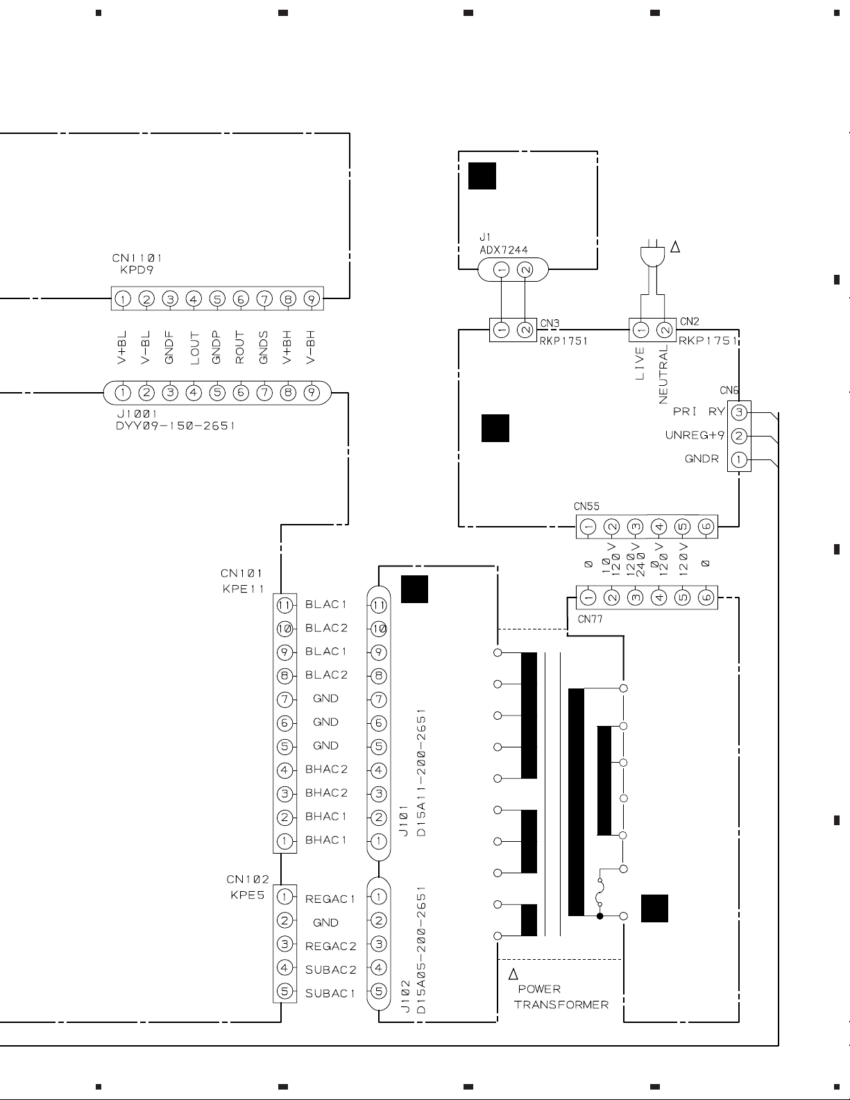
Page 12
1
23
HTV-SW1, HTV-C1
3.1.2 AFPS, PT SEC, PT PRI, STANDBY PT, and PW SWITCH ASSY
E-VOLUME & TONE CONTROL, SUBWOOFERLEVEL
BALANCE IN
A
1/2
1
CN1105
G
2/2
1/2
4
4.5
B
2
C
OE(OUTPUT) CONTROL
L/R MIX
LPF 180Hz
1/2
1/2
2/2
I/O EXPANDER
7.6
2/2
2/2
AFPS ASSY (AWU7262)
A
40.3
18.2
5.1
26.9
18.4
–40.3
–26.9
D
–18.6
12
A
1234
–18.8
Page 13

5
678
HTV-SW1, HTV-C1
BUFFER AMP
2/2
1/2
40Hz +9.5dB
HPF
1/2
2/2
HPF 180Hz
2/2
1/2
: AUDIO SIGNAL ROUTE(Lch)
: AUDIO SIGNAL ROUTE(SWch)
A
F
CN1101
B
F
CN1102
Q1001, Q1002 :
PROTECTION (SPEAKER)
RELAY DRIVER
PT SEC ASSY
B
(AWU7265)
0.1
POWER
TRANS-
FORMER
0.8
0.8
C
PT PRI ASSY
(AWU7264)
VEF1040
CN77
AKP7038
5.1
CN55
AKP7038
11.6
9.9
FU2,FU3:
REK1024
(T1.6AL250V)
FU1:
REK1027(T3.15AL250V)
H1- H6 : AKR7001
ATT7027
PW SWITCH
E
ASSY(AWU7259)
G
CN1104
AC POWER CORD
VDG1058
AC110 -127V/
220-230V/240V
50/60Hz
S1: Power SW
S2: Voltage
-Selector
S3: Voltage
-Sslector
C
D
T1
ATS7228
• NOTE FOR FUSE REPLACEMENT
CAUTION -
FOR CONTINUED PROTECTION AGAINST RISK OF FIRE,
REPLACE WITH SAME TYPE AND RATINGS ONLY.
5
G
J6
STANDBY PT ASSY (AWU7267)
D
A
6
7
B C
D
E
8
13
Page 14
1
HTV-SW1, HTV-C1
3.1.3 PAMP ASSY
A
J1001
A
B
23
PAMP ASSY(AWU7263)
F
4
26.9
–26.9
–25.7
25.8
J1002
C
A
5
40.2
12
–12
6
4
3
6
–40.2
D
14
F
1234
SW
Page 15
5
R
678
HTV-SW1, HTV-C1
A
: AUDIO SIGNAL ROUTE(Lch)
: AUDIO SIGNAL ROUTE(SWch)
CAUTION : FOR CONTINUED PROTECTION AGAINST RISK OF FIRE,
REPLACE ONLY WITH SAME TYPE NO. 491.500 MFD, BY
LITTELFUSE INK. FOR IC1201 (AEK7005).
Q1201, Q1202 : MUTE
.8
13.7
7
PROTECTION CIRCUIT
B
C
SW
40.3
2SC5198(P)
5
SPEAKE
5
2SA1941(P)
–40.3
SW ch DISCRETE POWER AMP
5
OVER LOAD
DETECTOR
D
15
F
6
7
8
Page 16
1
HTV-SW1, HTV-C1
3.1.4 JACK ASSY
23
4
A
TO CONTROL CENTER HTV-CI
JA4001
H
: AUDIO SIGNAL ROUTE(Lch)
D
CN6
B
A
CN1005
C
A
CN1004
G
TO CONTROL CENTER HTV-CI
D
16
CN501
H
JACK ASSY(AWU7257)
G
1234
Page 17

A
Waveforms
(HTV-A1)
HTW-SW1, HTV-C1
Note: The encircled numbers denote measuring
point in the schematic diagram.
CN1005-5 pin (LCHN), 6 pin (LCHP)
1
V : 20mV/div. H : 0.2mS/div.
Measurement condition :
Input a 1 kHz, 200mV signal to INPUT 1(2)
LCHP
LCHN
F
Waveforms
Q1109 Base
3
V : 20mV/div. H : 5mS/div.
Measurement condition :
SW ch output signal f=100Hz, 1W
Q1105 Collector, Q1106 Collector
6
V : 0.5V/div. H : 5mS/div.
Measurement condition :
SW ch output signal f=100Hz, 1W
(HTV-A1)
GND
GND
GND
IC8001- 2 pin (DATA), 3 pin (CLOCK),
2
4 pin (LCK) V: 0.5V/div. H: 1mS/div.
Measurement condition : Volume Min → 1
DATA
CLOCK
LCK
Q1110 Emitter
4
V : 50mV/div. H : 5mS/div.
Measurement condition :
SW ch output signal f=100Hz, 1W
D1309 Cathode
7
V : 1V/div. H : 10mS/div.
GND
GND
GND
GND
Q1101 Base, Q1102 Base
5
V : 0.5V/div. H : 5mS/div.
Measurement condition :
SW ch output signal f=100Hz, 1W
Q1101
Base
Q1102
Base
GND
GND
Q1105
Collector
Q1106
Collector
K
Waveforms
IC5001-45 pin (P1)
1
V : 1V/div. H : 1mS/div.
Waveforms
H
CN3001-9 pin (SCK), 10 pin (RVDT),
4
11 pin (REDY)
V : 0.5V/div. H : 0.5mS/div.
Measurement condition :
SUR. MODE OFF → VD
SCK
RVDT
REDY
( HTV-C1)
( HTV-C1)
GND
GND
GND
GND
GND
GND
IC5001-62 pin (1G)
2
V : 1V/div. H : 1mS/div.
CN501-4 pin (AC1):CH1, 8 pin (AC2):CH2
5
V : CH1:2V/div. , CH2:0.5V/div.
H : 1mS/div.
Measurement condition :
POWER ON (Connect with HTV-A1)
AC1
AC2
GND
GND
GND
GND
CN3001-6 pin (CLK), 7 pin (DATA),
3
8 pin (LCK) V: 0.5V/div. H: 1mS/div.
Measurement condition : Volume Min → 1
CLK
DATA
LCK
CN501-4 pin (AC1):CH1, 8 pin (AC2):CH2
5
V : CH1:2V/div. , CH2:0.5V/div.
H : 1mS/div.
Measurement condition :
STANDBY (Connect with HTV-A1)
AC1
AC2
GND
GND
GND
GND
GND
17
Page 18

1
HTV-SW1, HTV-C1
3.2 HTV-C1
A
3.2.1 OVERALL CONNECTIONS
B
23
INPUT LEV. ASSY
I
(AWU7252)
4
K
DISPLAY ASSY
C
D
(AWU7260)
H
MAIN ASSY
(AWU7261)
18
1234
Page 19

5
678
HTV-SW1, HTV-C1
A
B
Voltages of MAIN Assy
IC3001 (CXD2724Q) (V)
CONDITION SURROUND MODE
No. Pin Name OFF VD ST WIDE
10 D5V 4.9 4.9 4.9
16 XRST 5.0 5.0 5.0
18 CSL1 4.9 4.9 4.9
22 RDAV 5.0 5.0 5.0
23 ROUT 2.5 2.9 2.9
24 RADV 5.0 5.0 5.0
26 RINOP 2.4 2.4 2.4
27 RIN 2.4 2.4 2.4
28 CDAV 5.0 5.0 5.0
31 CLKV 5.0 5.0 5.0
32 XTLO 2.5 2.5 2.5
33 XTLI 2.5 2.5 2.5
37 SDAV 5.0 5.0 5.0
38 LIN 2.4 2.4 2.4
39 LINOP 2.4 2.4 2.4
41 LADV 5.0 5.0 5.0
42 LOUT 2.5 2.9 2.9
43 LDAV 5.0 5.0 5.0
46 SCK 5.0 5.0 5.0
47 READY 4.9 4.9 4.9
49 XLAT 5.0 5.0 5.0
50 RVDT 5.0 5.0 0.0
51 XS24 4.9 4.9 4.9
52 D5V 4.9 4.9 4.9
73 D5V 4.9 4.9 4.9
J
TERMINAL ASSY
(AWU7251)
FROM
SW AMP UNIT
(HTV–A1)
JACK ASSY
G
CN1003
TO
SW AMP UNIT
(HTV–A1)
JACK ASSY
G
JA4501
C
D
19
5
6
7
8
Page 20

1
MAIN ASSY
(AWU7261)
H
CN5001
K
43
VTL1096
VTL1096
VTL1096
VTL1096
VTL1096
VTL1096
DOLBY VIRTUAL DECODER
INPUT 1 INPUT 2
0V 4.5V
23
HTV-SW1, HTV-C1
3.2.2 MAIN, INPUT LEV. and TERMINAL ASSY
4
A
B
C
D
20
H
1234
Page 21

5
678
HTV-SW1, HTV-C1
INPUT LEV. ASSY
I
(AWU7252)
: AUDIO SIGNAL ROUTE (Lch)
A
B
-18.7
-28
LEVEL IN
-40.9
A
B
-13.5
STANDBY POWER ON
12.2V 11.6V
A
0V
B
11.5
9.5V
G
JA4501
(HTV-A1)
C
FRONT
SPEAKER
5
TERMINAL
J
ASSY
(AWU7251)
D
CN1003
G
(HTV-A1)
J
21
H
5
6
7
I
8
Page 22

1
HTV-SW1, HTV-C1
3.2.3 DISPLAY ASSY
A
DISPLAY ASSY
K
(AWU7260)
REMOCON
23
5.6
4
4.8
INPUT1 INPUT2
4.7V 0V
MUTE1
MUTE2
B
H
CN3001
C
0V 4.7V
Power Detect
RESTE
Each push on the button Voltage (v)
POWER SUR. DISP VOL– VOL+ INPUT No push on
0 0.8 1.6 2.5 3.3 4 4.6
D
22
K
1234
S5001 : INPUT
S5002 : VOL+
S5003 : VOL–
S5004 : DISPLAY
S5005 : SURROUND MODE
S5006 : POWER(STAND BY/ON)
Page 23

5
678
HTV-SW1, HTV-C1
A
-28
2
B
1
¶ In regard to the voltage at pin 22 of IC5001 (LEVEL IN)
• This terminal monitors the input signal level for operation of the
automatic standby mode.
• When INPUT key (INPUT 2) is selected and -46dB V (about 5mV rms)
is applied as input (input to both channels, freq. =1kHz), this terminal
rises to about 0.8V DC (in case of both channels, -40 dB V, about 0.8V
DC) and POWER ON is effected.
C
D
K
5
6
7
8
23
Page 24

1
23
HTV-SW1, HTV-C1
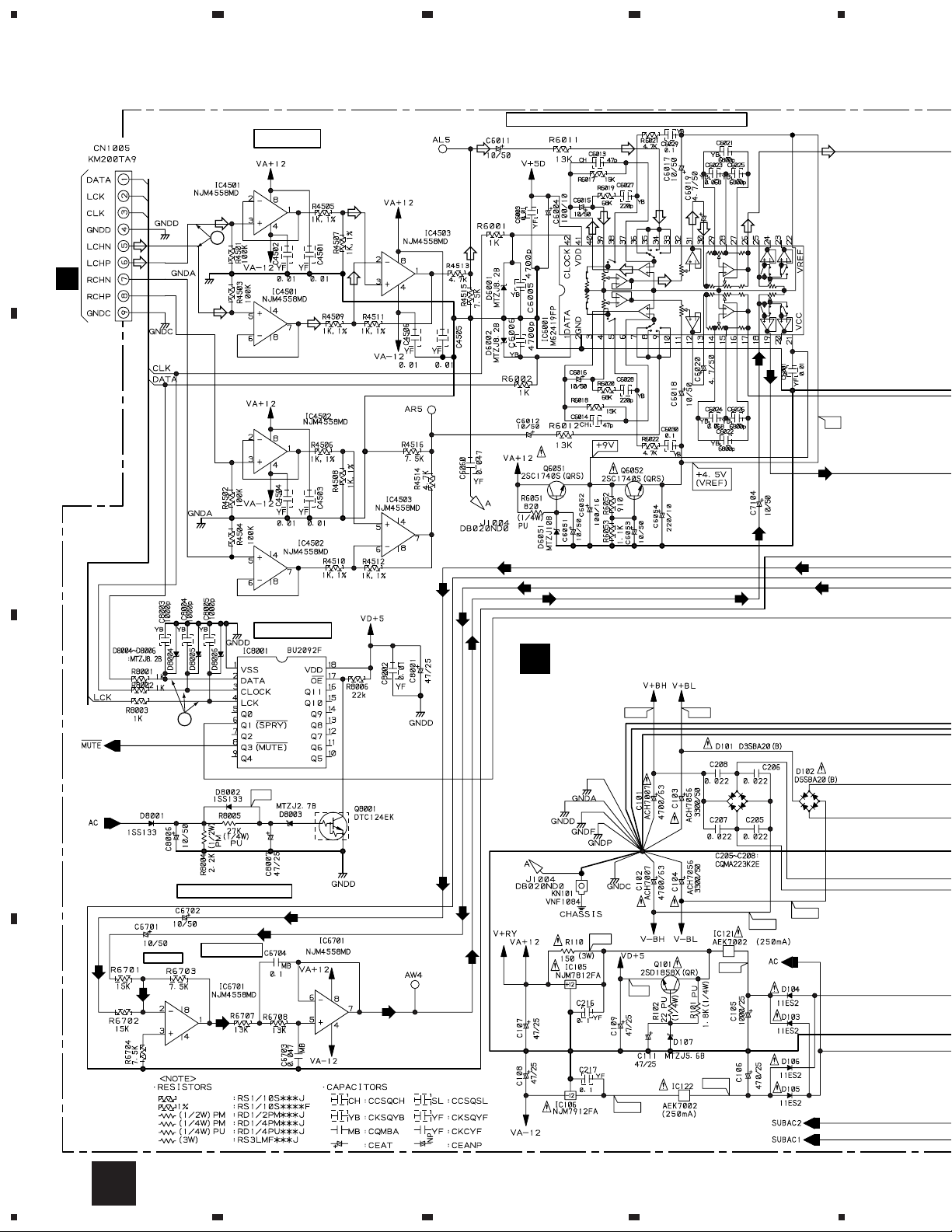
4. PCB CONNECTION DIAGRAM
4.1 HTV-A1
4.1.1 AFPS, PT SEC and PT PRI ASSY
A
NOTE FOR PCB DIAGRAMS :
1. Part numbers in PCB diagrams match those in the schematic
diagrams.
2. A comparison between the main parts of PCB and schematic
diagrams is shown below.
Symbol In PCB
Diagrams
BCE
B
BCE
D
Symbol In Schematic
Diagrams
BCEBCE
BCE
DGGSS
BCE
DGS
Part Name
Transistor
Transistor
with resistor
Field effect
transistor
CN1105
G
CN1104
G
AFPS ASSY
A
4
Resistor array
3-terminal
regulator
3. The parts mounted on this PCB include all necessary parts for
several destinations.
For further information for respective destinations, be sure to
check with the schematic diagram.
4. View point of PCB diagrams.
Connector
C
P.C.Board
Capacitor
Chip Part
SIDE A
SIDE B
PT SEC ASSY
B
T1 POWER TRANSFORMER
(ANP7288-B)
IC110 IC111 IC103 IC101 IC102
T1 POWER TRANSFORMER
C
D
24
A
B C
1234
PT PRI ASSY
SIDE A
D
(ANP7288-B)
CN55
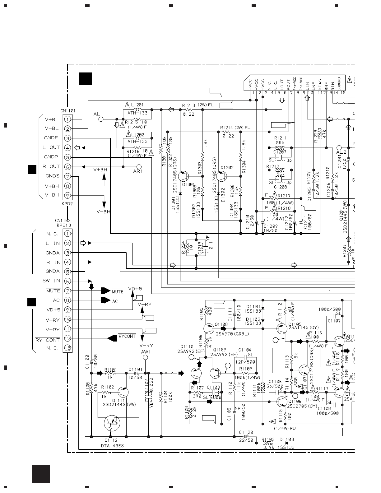
Page 25

5
C
678
HTV-SW1, HTV-C1
CN1101
F
Q102
IC105
IC121
IC122
Q105
IC106
Q6051
A
Q103
Q104
Q101
B
Q6052
CN1102
F
C
NP7288-B)
102
Q1005
Q1001
Q1002
Q1004
Q303
Q301
D
8-B)
Q302
SIDE A
(ANP7288-B)
A
5
6
7
8
25
Page 26

1
HTV-SW1, HTV-C1
A
IC4502
IC4501
IC4503
23
AFPS ASSY
A
4
B
C
IC6001
Q106
IC6031
IC6501
IC6701
IC7101
Q1003
IC8001
Q8001
D
SIDE B
(ANP7288-B)
26
A
1234
Page 27

5
678
HTV-SW1, HTV-C1
A
B
PT SEC ASSY
B
PT PRI ASSY
C
C
(ANP7288-B)
D
SIDE B
5
6
7
(ANP7288-B)
A
B C
8
27
Page 28

1
HTV-SW1
4.1.2 STANDBY PT, PW SWITCH ASSY
STANDBY PT ASSY
D
A
CN77
C
23
SIDE A
4
J6
G
AC
POWER
CORD
B
LIVE
NEUTRAL
(ANP7289-B)
E
PW SWITCH
ASSY
STANDBY PT ASSY
D
C
SIDE B
D
(ANP7289-B)
28
D
E
1234
Page 29

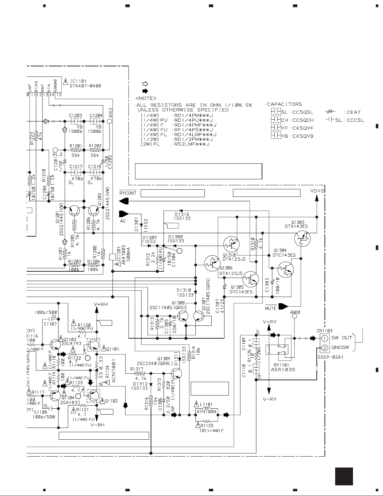
1
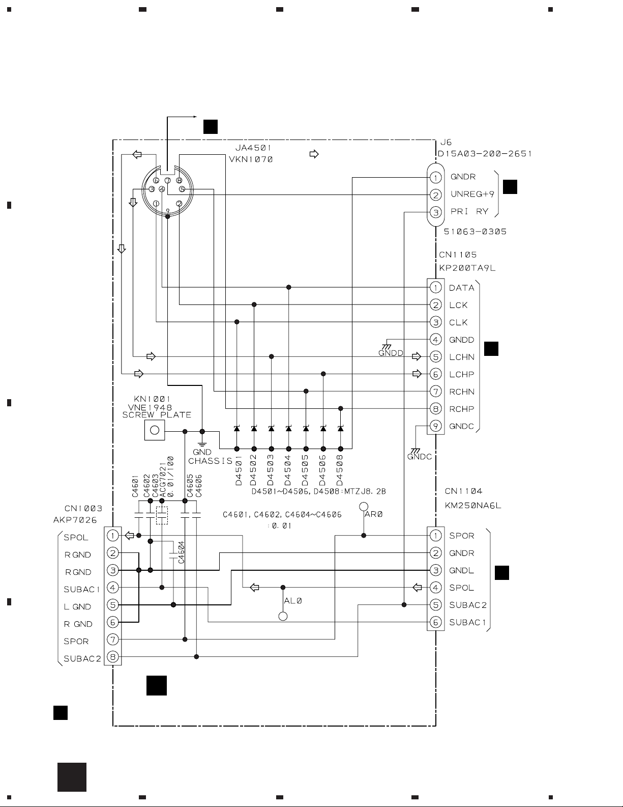
4.1.3 JACK ASSY
JACK ASSY
G
234
HTV-SW1
A
CN6
D
SIDE A
TO
CONTROL
CENTER
HTV-C1
CN501
H
FROM
CONTROL
CENTER
HTV-C1
JA4001
H
JACK ASSY
G
(ANP7288-B)
SIDE B
CN1004
A
CN1005
A
B
C
(ANP7288-B)
D
G
1
2
3
4
29
Page 30

1
HTV-SW1, HTV-C1
4.1.4 PAMP ASSY
23
4
A
PAMP ASSY
F
SW
SPEAKER
B
Q1104 Q1309 Q1106
Q1102
PAMP ASSY
F
C
D
Q1107
Q1110 Q1111
Q1109 Q1108
Q1103 Q1105
Q1101
Q1112
30
F
1234
Page 31

5
678
HTV-SW1, HTV-C1
A
J1002
A
J1001
SIDE A
A
B
1112 Q1303
Q1306
Q1310
Q1305 Q1202
Q1304
IC1201
Q1201 Q1204 Q1203 Q1307
IC1101
Q1308
SIDE B
(ANP7288-B)
Q1302
Q1301
C
D
(ANP7288-B)
F
5
6
7
8
31
Page 32

1
HTV-SW1, HTV-C1
4.2 HTV-C1
4.2.1 MAIN ASSY
A
23
4
MAIN ASSY
H
FROM
B
SW AMP UNIT
HTV-A1
CN1003
G
SIDE A
IC501
IC502
IC504
IC505
IC507
IC506
IC503
K
CN5001
Q551
CN203
J
TO
SW AMP UNIT
HTV-A1
JA4501
G
I
CN4002
Q501
Q553
IC551
C
IC3001
D
(ANP7287-A)
CN4001
I
32
H
1234
Page 33

5
678
HTV-SW1, HTV-C1
A
MAIN ASSY
H
SIDE B
B
Q552
Q554
C
IC3501
IC2002
Q2003
Q2001
Q2002
IC2001
IC3001
Q2031
Q2032
(ANP7287-A)
5
6
7
Q2012
Q2011
H
8
D
33
Page 34

1
23
HTV-SW1, HTV-C1
4.2.2 INPUT LEV., TERMINAL and DISPLAY ASSY
A
INPUT LEV. ASSY
I
4
SIDE A
(ANP7287-A)
CN552
H
B
FRONT
SPEAKER
C
DISPLAY ASSY
K
TERMINAL ASSY
J
(ANP7287-A)
CN3001
H
H
H
CN551
CN503
D
(ANP7287-A)
34
I
J K
1234
Page 35

5
678
HTV-SW1, HTV-C1
INPUT LEV. ASSY
I
IC4002 IC4001 IC2511
J
TERMINAL ASSY
SIDE B
(ANP7287-A)
A
B
(ANP7287-A)
DISPLAY ASSY
K
(ANP7287-A)
Q5004 Q5009 IC5001 Q5001 Q5008 Q5007
I
5
6
7
J K
8
C
D
35
Page 36

HTV-SW1, HTV-C1
5. PCB PARTS LIST
NOTES :
Parts marked by “ NSP ” are generally unavailable because they are not in our Master Spare Parts List.
The mark found on some component parts indicates the importance of the safety factor of the part.
Therefore, when replacing, be sure to use parts of identical designation.
When ordering resistors, first convert resistance values into code form as shown in the following examples.
Ex. 1 When there are 2 effective digits (any digit apart from 0), such as 560 ohm and 47k ohm (tolerance is shown by
J = 5%, and K = 10%).
1
560 Ω = 56 × 10
47k Ω = 47 × 10
= 561................................................... RD1/4PU 5 6 1 J
3
= 473 .................................................. RD1/4PU 4 7 3 J
0.5 Ω = R50 ...................................................................... RN2H Â 5 0 K
1 Ω = 1R0 ......................................................................... RS1P 1 Â 0 K
Ex. 2 When there are 3 effective digits (such as in high precision metal film resistors).
5.62k Ω = 562 × 10 1 = 5621 ........................................... RN1/4PC 5 6 2 1 F
Mark No. Description Part No.
5.1 HTV-A1
LIST OF PCB ASSEMBLIES
MOTHER ASSY AWM7419
SUB ASSY AWX7293
AFPS ASSY
SEMICONDUCTORS
IC121,IC122 (250mA) AEK7002
IC105 NJM7812FA
IC106 NJM7912FA
Q6051,Q6052 2SC1740S
Q101 2SD1858X
D103-D106 11ES2
D101 D3SBA20(B)
D102 D5SBA20(B)
RELAY
CAPACITORS
C101,C102 (4700µF/63V) ACH7007
C103,C104 (3300µF/50V) ACH7056
AFPS ASSY AWU7262
PAMP ASSY AWU7263
PT PRI ASSY AWU7264
PT SEC ASSY AWU7265
JACK ASSY AWU7257
STANDBY PT ASSY AWU7267
PW SWITCH ASSY AWU7259
A
IC8001 BU2092F
IC6001 M62419FP
IC4501-IC4503,IC6031 NJM4558MD
IC6501,IC6701 NJM4558MD
IC7101 NJM4558MD
Q1002,Q1005 2SC1740S
Q1001 DTA143ES
Q8001 DTC124EK
D1001,D1002,D8001,D8002 1SS133
D6051 MTZJ10B
D8003 MTZJ2.7B
D107 MTZJ5.6B
D6001,D6002,D8004-D8006 MTZJ8.2B
RY1002 ASR1035
C6013,C6014 CCSQCH470J50
C7102,C7103 CEANPR47M50
C6011,C6012,C6015-C6018 CEAT100M50
Mark No. Description Part No.
C6031,C6032,C6051,C6053 CEAT100M50
C6701,C6702,C7104,C7105,C8006 CEAT100M50
C6004 CEAT101M10
C6052 CEAT101M16
C105 CEAT102M25
C6054 CEAT221M10
C6503,C6504 CEAT2R2M50
C106 CEAT471M25
C107-C109,C111,C8001,C8007 CEAT470M25
C6019,C6020 CEAT4R7M50
C8003-C8005 CKSQYB102K50
C6029,C6030 CKSQYB104K25
C6027,C6028 CKSQYB221K50
C6005,C6006 CKSQYB472K50
C6021,C6022,C6025,C6026 CKSQYB682K50
C6023,C6024 CKSQYB683K25
C4501-C4506,C6001,C6003,C8002 CKSQYF103Z50
C1001-C1004,C216,C217 CKSQYF104Z50
C6060 CKSQYF473Z50
C205-C208 CQMA223K2E
C6704 CQMBA104J50
C6501,C6502,C6703 CQMBA473J50
RESISTORS
R8004 RD1/2PM222J
R1001,R1002 RD1/4PM100J
R101 RD1/4PU182J
R102 RD1/4PU220J
R8005 RD1/4PU273J
R6051 RD1/4PU821J
R4505-R4512 RS1/10S1001F
R110 RS3LMF151J
Other Resistors RS1/10S J
OTHERS
CABLE HOLDER (9P) 51052-0900
CABLE HOLDER (13P) 51063-1305
J1002 JUMPER WIRE D15A13-150-2651
J1004 BOARD IN WIRE DB020ND0
CN1005 9P PLUG KM200TA9
CN1004 SOCKET 6-P KP250NA6
CN101 CONNECTOR (11P) KPE11
CN102 CONNECTOR (5P) KPE5
KN101 EARTH METAL FITTING VNF1084
36
Page 37

HTV-SW1, HTV-C1
Mark No. Description Part No. Mark No. Description Part No.
PT SEC ASSY
B
SEMICONDUCTORS
IC103 (1A) AEK7009
IC101,IC102 (1.25A) AEK7010
IC110,IC111 (7A) AEK7021
CAPACITORS
C123 (0.01µF) ACG7021
C121,C122 CKSQYF103Z50
OTHERS
CABLE HOLDER (5P) 51063-0505
J102 JUMPER WIRE D15A05-200-2651
J101 JUMPER WIRE D15A11-200-2651
PT PRI ASSY
C
CABLE HOLDER (11P) 51063-1105
OTHERS
CN77 6P CONNECTOR AKP7038
STANDBY PT ASSY
D
PCB BINDER VEF1040
SEMICONDUCTORS
IC1 (315mA) AEK7003
D3 S1VB20/F03
D1,D2 1SS133X
TRANSFORMER
T3 ATT7027
RELAY
RY1 ASR7019
CAPACITORS
C1,C3,C4 (1000pF/AC250V) ACG7020
C5 (0.01µF/AC250V) ACG1005
C6 CEAT102M25
OTHERS
CN55 6P CONNECTOR AKP7038
CN2,CN3 AC CORD SOCKET RKP1751
S3 VOLTAGE SELECTOR AKX7004
S2 VOLTAGE SELECTOR AKX7006
PW SWITCH ASSY
H1– H6 FUSE CLIP AKR7001
CN6 CONNECTOR (3P) KPE3
PCB BINDER VEF1040
E
SWITCH
S1 ASM7002
OTHERS
J1 CONNECTOR ASSY 2P ADX7244
Q1108 2SA970
Q1109,Q1110 2SA992
Q1107 2SC1740S
Q1301,Q1302,Q1307,Q1308 2SC1740S
Q1309 2SC2240
Q1106 2SC2705
Q1103 2SC4793
Q1101 2SC5198(P)
Q1111,Q1201,Q1202 2SD2144S
Q1306,Q1310 DTA123JS
Q1112,Q1303 DTA143ES
Q1304,Q1305 DTC143ES
D1307,D1309 11ES2
D1101-D1103,D1301-D1304, 1SS133
D1308,D1310-D1312,D1316 1SS133
COILS
L1201,L1202 AF CHOKE COIL ATH-133
L1101 AF CHOKE COIL ATH1004
RELAY
RY1101 ASR1035
CAPACITORS
C1107,C1108 CCCSL101K2H
C1104 CCCSL120K2H
C1106 CCCSL5R0C2H
C1207,C1208 CCSQSL3R0C50
C1217,C1218 CCSQSL471J50
C1103 CCSQSL681J50
C1101 CEAT100M50
C1211,C1212 CEAT101M50
C1105 CEANP101M50
C1306 CEANP2R2M50
C1100,C1205,C1206,C1209 CEAT100M50
C1210,C1304 CEAT100M50
C1111,C1303 CEAT101M10
C1201,C1202 CEAT1R0M50
C1120 CEAT220M50
C1305 CEAT221M10
C1307 CEAT470M25
C1203,C1204 CKSQYB152K50
C1102 CKSQYB223K50
C1109,C1110,C1219 CKSQYF104Z50
RESISTORS
R1124 (0.33Ω,5W) ACN7001
R1126 RD1/2PM100J
R1217,R1218 RD1/4LMF101J
R1109 RD1/4PM104J
R1110 RD1/4PM112J
R1125,R1215,R1216 RD1/4PMF100J
R1116-R1119 RD1/4PMF101J
R1112 RD1/4PMF680J
R1312 RD1/4PU222J
R1315 RD1/4PU821J
PAMP ASSY
F
SEMICONDUCTORS
IC1201 (500mA) AEK7005
IC1101 STK407-040B
Q1104 2SA1837
Q1102 2SA1941(P)
Q1105 2SA1145
R1115 RF1/4PS101J
R1120-R1123 RF1/4PS4R7J
R1213,R1214 RS2LMFR22J
Other Resistors RS1/10S J
OTHERS
CN1103 2P CONNECTOR 5569-02A1
CN1101 9P JUMPER CONNECTOR KPD9
CN1102 CONNECTOR (13P) KPE13
37
Page 38

HTV-SW1, HTV-C1
Mark No. Description Part No. Mark No. Description Part No.
JACK ASSY
G
SEMICONDUCTORS
D4501-D4506,D4508 MTZJ8.2B
CAPACITORS
C4603 (0.01µF/100V) ACG7021
C4601,C4602,C4604-C4606 CKCYF103Z50
OTHERS
CN1003 8P CONNECTOR AKP7026
J6 JUMPER WIRE D15A03-200-2651
CN1104 PLUG 6-P KM250NA6L
CN1105 9P SOCKET KP200TA9L
CABLE HOLDER (3P) 51063-0305
PCB BINDER VEF1040
I/O JACK VKN1070
SCREW PLATE VNE1948
5.2 HTV-C1
LIST OF PCB ASSEMBLIES
COMPLEX ASSY AWM7418
DISPLAY ASSY AWU7260
MAIN ASSY AWU7261
TERMINAL ASSY AWU7251
INPUT LEV. ASSY AWU7252
MAIN ASSY
H
SEMICONDUCTORS
IC501,IC502 (630mA) AEK7006
IC503,IC551 (200mA) AEK7023
IC504 BA05T
IC2001 BU4066BCF
IC3001 CXD2724Q
TRANSFORMER
T2 ATT7025
CAPACITORS
C500 (0.01µF/AC250V) ACG1005
C591 (0.01µF/100V) ACG7021
C3204,C3209,C3285-C3288,C3295CCSQCH101J50
C3206,C3207 CCSQCH120J50
C3517-C3520 CCSQSL331J50
C2021,C2023,C504-C506,C509 CEAT100M50
C511 CEAT100M50
C552 CEAT101M10
C503 CEAT101M63
C501 CEAT222M25
C502 CEAT331M25
C3201-C3203,C3523,C3524 CEAT470M25
C507,C508 CEAT470M50
C3282,C3292 CEAT471M6R3
C3511,C3512 CEAT4R7M50
C2031,C3296,C3515,C3516 CKSQYB102K50
C3205,C3208 CKSQYB331K50
C2005,C2015,C2022,C2024 CKSQYF103Z50
C3283,C3284,C3289-C3291 CKSQYF103Z50
C3293,C3294,C3513,C3514 CKSQYF103Z50
C534-C536,C540,C592 CKSQYF103Z50
RESISTORS
R556 RD1/4PU220J
R503 RD1/4PU223J
R502 RS1LMF122J
R560 RS3LMF101J
Other Resistors RS1/10S J
OTHERS
CN2001,CN2002 PIN JACK (4P) AKB7015
CN501 8P CONNECTOR AKP7026
X3201 CRYSTAL RESONATOR ASS7000
(33.8688MHz)
CN3001 FFC CONNECTOR 21P HLEM21S-1
IC507 NJM7805FA
IC2002,IC3501 NJM4558MD
IC505 NJM7806FA
IC506 NJM7906FA
Q501 2SB1238X
Q553 2SB1238X
Q2001,Q2002,Q2011,Q2012,Q554 2SC2412K
Q2031 DTA124EK
Q2003,Q2013 DTA143EK
Q2032 DTC124EK
D501-D505 11ES2
D553,D554 11ES2
D2001,D2002,D506,D555-D557 1SS133
D2003,D2013 DAP202K
D507 MTZJ27D
D4001-D4003,D4007,D4008 MTZJ8.2B
D4017,D4018 MTZJ8.2B
D508 MTZJ9.1C
COILS
L4001-L4007 CHIP BEAD FILTER DTL1019
L2501 LAU1R0J
L3203 LFA220J
L3202 LFA6R8J
L501 FERRITE BEAD VTH1024
L2001- L2006 CHIP BEADS VTL1096
38
CN551 10P PLUG KM200TA10
CN552 6P PLUG KM200TA6
CN503 SOCKET 4-P KP250NA4
KN4001,KN501 VNF1084
INPUT LEV. ASSY
I
I/O JACK VKN1070
EARTH METAL FITTING
SEMICONDUCTORS
IC2511,IC4001,IC4002 NJM4558MD
D2510,D2512 1SS133
D2513 MTZJ4.3B
CAPACITORS
C2513,C2518 CCSQCH220J50
C4001,C4002,C4011,C4012 CEAT100M50
C2511 CEAT1R0M50
C2514,C2515,C2519,C2522,C4051CEAT470M25
C4053 CEAT470M25
C2520,C2521,C4071,C4072 CEAT4R7M50
C4052,C4054,C4056,C4058 CKSQYF103Z50
RESISTORS
R2528 RD1/4PU101J
R4003-R4006 RS1/10S1002F
Other Resistors RS1/10S J
Page 39

Mark No. Description Part No.
OTHERS
CN4002 10P SOCKET KP200TA10L
CN4001 6P SOCKET KP200TA6L
TERMINAL ASSY
J
OTHERS
CN203 4-P PLUG KM250NA4L
KN201 SCREW PLATE VNE1948
DISPLAY ASSY
K
SEMICONDUCTORS
IC5001 PDG239A
Q5009 2SC2412K
Q5007,Q5008 DTA143EK
Q5001,Q5004 DTC143EK
D5002,D5008-D5011,D5013 1SS133
D5007 GL3ED8
D5012 MTZJ3.0B
D5003 MTZJ6.8B
D5005,D5006 SLP3118C51H
COIL
L5001 LAU220J
SWITCHES
S5001-S5006 ASG1034
CAPACITORS
C5025 (0.047F/5.5V) ACH1246
C5024 CCSQSL471J50
C5004 CEJA100M25
C5002,C5008 CEJA101M10
C5026 CEJA220M10
HTV-SW1, HTV-C1
6. ADJUSTMENT
There is no information to be shown in this chapter.
C5023 CKSQYB472K50
C5001,C5003,C5007,C5013 CKSQYF103Z50
C5006 CKSQYF473Z50
RESISTORS
R5017 RA15T473J
R5016 RA9T473J
R5007 RD1/4PU821J
Other Resistors RS1/10S J
OTHERS
V5001 FL TUBE AAV7052
X5001 CERAMIC RESONATOR DSS1053
CN5001 FFC CONNECTOR 21P XKP3021
(8MHz)
REMOTE RECEIVER UNIT GP1U28X
FL HOLDER VNF1085
39
Page 40

HTV-SW1, HTV-C1
7. GENERAL INFORMATION
7.1 PARTS
7.1.1 IC
BU2092F (IC8001: AFPS ASSY)
¶ The information shown in the list is basic information and may not
Serial In/Parallel Out Driver
Pin Function Block Diagram
DD
V
OE
Q11
Q10
Q9
Q8
Q7
Q6
Q3
Q5
Q4
18 17 16 15 14 13 12 11 10
Output Buffer (Open Drain)
Control Circuit
12 bits Shift Register
12 bits Strage Register
123456789
Q0
Q1
Vss
DATA
LCK
CLOCK
Q2
No. Name I/O Description
1 Vss – GND
2 DATA I Serial data input
3 CLOCK I Shift lock for data ( )
4 LCK I Lutch clock for data ( )
5Q0
16 Q11
17 OE I Output enable (H: output, FET: OFF)
18 VDD – Power supply
M62419FP (IC6001: AFPS ASSY)
Electronic Volume Control with Tone Function
correspond exactly to that shown in the schematic diagrams.
Parallel data output (Nch Open Drain FET)
||O
Lutch Data L H
Output FET ON OFF
Block Diagram
CLOCK
CLOCK
I/F
DATA
DATA
VDD
SELECT OUT 2
DD
V
GND
SELECT OUT 1
VOL IN 2
LOUD IN 2
VOL IN 1
LOUD IN 1
SELECT 2 NF 2
SELECT 2 IN A
SELECT 2 IN B
–
+
+
–
–
+
+
–
SELECT 1 IN A
SELECT 2 NF 1
SELECT 1 IN B
SELECT 2 IN C
SELECT 2 IN D
ATTF OUT 2
SELECT 1 IN C
ATTF OUT 1
SELECT 1 IN D
ATTR OUT 2
TONE IN 2
+
–
–
+
TONE IN 1
ATTR OUT 1
TC 2 A
TC 1 A
TC 2 B
–
+
+
–
TC 1 B
TC 2 C
TC 1 C
TONE OUT 2
FADER IN 2
+
+
FADER IN 1
TONE OUT 1
REAR OUT 2
FRONT OUT 2
2242 41 40 39 38 37 36 35 34 33 32 31 30 29 28 27 26 25 24 23
+
–
–
Vref
–
–
+
211234567891011121314151617181920
REAR OUT 1
FRONT OUT 1
VREF
Vcc
Vcc
40
Page 41

Pin Function
HTV-SW1, HTV-C1
No. Name Description
1 DATA Control data input terminal.
Data are entered synchronized to CLOCK.
2 GND Ground terminal
3 SELECT OUT1 Output terminals of the input selector switch
4 VOL IN1 Input terminals of the volume control section
5 LOUD IN1 Frequency characteristic setting terminal of
the loudness section
6 SELECT2 NF1 Each input gain is adjusted by the resistor
connected between this terminal and the
SELECT OUT terminal and the resistor added
between IN A and IN D.
7 SELECT1 IN A Input terminal for channel 1 of the input selector
switch section
8 SELECT1 IN B
9 SELECT1 IN C
10 SELECT1 IN D
11 ATTF OUT1 Output terminals of the volume control section
(initial stage). Connect by C connection to the
VREF terminal 22 for reduction of the switching
noise.
12 ATTR OUT1 Output terminals of the volume control section
(last stage)
13 TONE IN1 Input terminals of the tone control section
14 TC1 A Frequency characteristic setting terminals of
the tone control section for channel 1
15 TC1 B
No. Name Description
24 REAR OUT2 Output terminals of the fader volume control
section (rear)
25 FADER IN2 Input terminals of the fader volume control section
26 TONE OUT2 Output terminals of the tone control section
27 TC2 C Frequency characteristic setting terminals of
the tone control section for channel 2
28 TC2 B
29 TC2 A
30 TONE IN2 Input terminals of the tone control section
31 ATTR OUT2 Output terminals of the volume control section
(last stage)
32 ATTF OUT2 Output terminals of the volume control section
(initial stage). Connect by C connection to the
VREF terminal 22 for reduction of the switching
noise.
33 SELECT2 IN D Input terminal for channel 2 of the input selector
switch section
34 SELECT2 IN C
35 SELECT2 IN B
36 SELECT2 IN A
37 SELECT2 NF2 Each input gain is adjusted by the resistor
connected between this terminal and the
SELECT OUT terminal and the resistor added
between IN A and IN D.
38 LOUD IN2 Frequency characteristic setting terminal of
the loudness section
16 TC1 C
17 TONE OUT1 Output terminals of the tone control section
18 FADER IN1 Input terminals of the fader volume control section
19 REAR OUT1 Output terminals of the fader volume control
section (rear)
20 FRONT OUT1 Output terminals of the fader volume control
section (front)
21 Vcc Analog power supply terminal
22 DATA IC signal ground. Impress 1/2 VCC.
23 FRONT OUT2 Output terminals of the fader volume control
section (front)
39 VOL IN2 Input terminals of the volume control section
40 SELECT OUT1 Output terminals of the input selector switch
41 VDD Digital power supply terminal
42 CLOCK Clock input terminal for serial data transfer
41
Page 42

HTV-SW1, HTV-C1
7.1.2 DISPLAY
AAV7052 (V5001: DISPLAY ASSY)
7 FL INDICATOR TUBE
• Pin Assignment
PATTERN AREA
1‡
• Pin Connection
NOTE 1) F1,F2 -------------- Filament
2) NP ------------------No pin
3) NX ------------------ No extend pin
4) DL ------------------ Datum Line
5) 1G - 9G ----------- Grid
• Grid Assignment
• Anode Connection
P1
P2
P3
1G - 8G
a1
a2
h
9G
P10
P11
P12
1G - 8G
c
e
r
9G
42
P4
P5
P6
P7
P8
P9
j
k
b
f
m
g
P13
P14
P15
P16
P17
p
n
d1
d2
Dp
Page 43

7.2 DIAGNOSIS
7.2.1 DISASSEMBYL (HTV-A1)
BONNET CASE
2
× 3
Bonnet
Case
3
HTV-SW1, HTV-C1
At this time, diagnosis of the
1
× 5
1
× 3
PAMP assembly is possible.
3
1
× 4
AFPS ASSY
× 2
PAMP Assy
5
4
× 2
1
× 3
1
× 4
9
8
10
AFPS Assy
Note: At the time of installation,
install so that the circuit boards
comes under the PCB stay claw.
PCB Stay
Claw
7
ST Barrier
6
AFPS assembly
DIAGNOSIS
1
× 2
1
AFPS Assy
2
× 3
PCB Holder
PAMP Assy
43
Page 44

HTV-SW1, HTV-C1
7.2.2 INDEPENDENT OPERATION DIAGNOSIS METHOD(HTV-A1)
In principle, the HTV-1 system operates only as a combination
of HTV-C1 and HTV-A1, but analysis from the electronic
volume control (M62419FP) on is possible according to the
following method.
Note: The white numbers in black circles in the drawing
correspond to the following step numbers.
1
Short-circuit W141 (PRIRY) and W142 (UNREG+9) in
the TANDBY PT assembly.
2
Short-circuit W215 (SPRY) and W216 (GNDD) in the
AFPS assembly.
[At the time of L/Rch analysis]
3
Disconnect C6031 in the AFPS assembly and apply the
signal to W251 (L ch IN). [In case of the right channel,
disconnect C6023 and apply the signal to W240 (R ch IN).]
÷ As the gain from L ch IN to L ch SP OUT is about 37 dB
(freq. = 1 kHz), input of 40 mVrms to L ch IN results in
output of 1 W (2.83 Vrms/8 Ω) at L ch SP OUT.
[At the time of SWch analysis]
4
Disconnect W131 (SW IN) in the PAMP assembly.
Apply the signal to the plus pole of CI100.
5
÷ As the gain from CI100 to SWch is about 38 dB
(freq. = 100 Hz), input of 36 mVrms to CI100 results in
output of 1 W (2.83 Vrms/8 Ω) at SWch SP OUT.
4
Take off theW131
PAMP ASSY
SIDE A
5
Enter an
signal input
AFPS ASSY
1
Shortcircuited
STANDBY PT ASSY
SIDE A
SIDE A
KN1001
JACK ASSY
KN101
AFPS ASSY
Caution items for diagnosis of the AF
PS assembly after removal from the
chassis
The assembly operates only when the earth
fittings KN101 (AFPS assembly) and KN10
01 (JACK assembly) are connected.
For diagnosis with the AFPS assembly remo
ved from the chassis, perform diagnosis with
these earth fittings short-circuited.
44
2
Short-circuited
Enter an signal input
Take off the C6031
3
3
Page 45

7.3 TEST MODE (HTV-C1)
HTV-SW1, HTV-C1
7.3.1 Entry into Test Mode
There are the following two methods for entry into test mode.
(1) Reception of the command "A55F" by remote control.
(2) Short-circuit the TEST MODE point (pin 19 of IC5001 and
GND) on the copper foil side of the DISPLAY assembly.
Connect the power cable to an outlet.
DISPLAY ASSY
K
IC5001
Pin 19
Short point
SIDE B
• In regard to the automatic standby mode
• Automatic standby mode always is reached during POWER ON.
• Standby condition is reached when the input signal disappears
for 5 minutes (input level of INPUT 1 (2): 49 dB V, LEVEL IN
voltage: 0.6 V DC). At this time, the standby indicator lights
orange.
• POWER ON occurs when an input signal is entered in this
condition ( a signal of -46dB V to INPUT 1 (2)).
• When the power is switched off with the STANDBY/ON key on
the unit or with the power key of the remote control unit, this
function does not operate and the standby indicator lights red.
2. DSP Check
Press the SURR. MODE key. = DSP check mode is entered.
DSP check mode
A test tone is put out at the time of DOLBY VIRTUAL condition.
Test tone output is repeated in the order of LEFT = CENTER =
RIGHT = SURROUND.
Confirm that DSP operates normally at the time of SURROUND
output.
Press the SURROUND MODE key twice. = DSP check mode is
canceled. FL and LED display normally.
• Keys other than the specified ones operate normally.
• At the time of entry into test mode, FL displays "TEST 1"
for 1 second.
• The LED flashes during test mode.
• At this time, the VOLUME setting becomes 10.
• The SURROUND mode becomes DOLBY VIRTUAL ON.
7.3.2 Test Mode Operation
FL segment check
Press the DISPLAY key. = The operations (1) to (5) are
switched sequentially.
(1) FL, LED all lit
(2) FL, LED all not lit
(3) (Segment check 1) Display of "ABCDEFGH"
(4) (Segment check 2) Display of "IJKLMNOP"
(5) Normal display
1. Confirmation of the Automatic Standby Function
(1) Press the INPUT key. =
The power is switched off and automatic standby mode
is entered. The standby indicator lights orange. (This
condition is reached when 5 minutes without a signal
have passed during power ON.)
(2) Apply an input signal to the INPUT terminal. =
AUTO POWER ON (This operates only with input to the
selected INPUT terminal.)
7.3.3. Test Mode Cancellation
During power ON, set the STANDBY/OFF key to OFF or disconnect
the power cable from the outlet.
45
Page 46

HTV-SW1, HTV-C1
7.4 INDEPENDENT OPERATION DIAGNOSIS METHOD (HTV-C1)
• In principle, the HTV-1 system operates only as a combination of
HTV-C1 and HTV-SW1, but operation is possible by applying
AC 26 V at the input side (bettween AC1 and AC2) of the
subtransformer (T2) in the MAIN assembly.
• In this case, it is not possible to check all functions (functions on
the HTV-A1 side).
• The gain from the pin jack [(INPUT 1 (2)] to AL6+ (-) or AR6+
(-) is as shown below.
SURR. MODE Gain (dB)
OFF -3.0dB
VD (EFFECT +3) -3.6dB
ST - WIDE -3.5dB
• With input of -14 dBV (200mV rms) to INPUT 1 (2), -17 dBV
appears at AL6+ (-), AR6+ (-) in case of SURR. OFF.
# In case of independent operation, a DC component appears at
AL6+ (-), AR6+ (-) depending on the signal level.
AC26V
MAIN ASSY
H
SIDE A
CAUTION :
• Caution and diagnosis method at the time of removal of the MAIN assembly from the chassis.
No operation occurs when the earth plates KN501 and KN4001 are not connected. When diagnosis is to be performed with the
MAIN assembly removed from the chassis, short-circuit the earth plates KN501 and KN4001 before diagnosis.
EARTH METAL FITTING KN501and KN4001at the short-circuit
MAIN ASSY
H
KN4001
CN501
CN503
SIDE A
CN3001
FRONT
T2
KN501
46
Page 47

7.5 IN REGARD to the BACKUP FUNCTION (HTV-C1)
Even when disconnected from the main power supply, HTV-C1 keeps the
following memory settings stored for about two weeks to one month
because of the backup power supply.
When these settings are changed at the time of servicing, they will remain changed,
so that caution is required. In this case, return to the factory settings is possible by
switching the power supply off after entry into test mode.
7 Function for memorizing of settings
* Input switching
* Bass
* Treble
* Balance
* SW level
* Sound mode
* Effect level
* Loudness ON/OFF
* Demonstration mode ON/OFF
* Volume (only in case of demonstration mode OFF)
HTV-SW1, HTV-C1
7 Settings at the time of shipping from the factory
* Input switching: INPUT1
* Bass: ±2
* Treble: ±0
* Balance: CENTER
* SW level: +1
* Surround mode: VIRTUAL DOLBY
* Effect level: +3
* Loudness: OFF
* Demonstration mode: ON
* Volume: MIN
47
Page 48

HTV-SW1, HTV-C1
7.3 BLOCK DIAGRAM
CONTROL CENTER
HTV–C1
Q2001,Q2011
2SC2412K
IC2001
BU4066BCF
NJM4558MD
IC2002
NJM4558MD
IC2511
IC3001
CXD2724Q
IC3501
NJM4558MD
IC4001(1/2)
NJM4558MD
IC4001(2/2)
NJM4558MD
Q5004
DTC143EK
Q5007
DTA143EK
D5007
GL3ED8
STANDBY
-INDICATOR
Q5008
DTA143EK
BA05T
NJM7805FA
NJM7806FA
NJM7906FA
11ES2
11ES2
2SB1238X
IC5001
PDG239A
(Interruption Detect)
Q553
2SB1238X
48
Page 49

AMPLIFIER
HTV–A1
HTV-SW1, HTV-C1
IC6001(1/2)
IC4503
NJM4558MD
BU2092F
M62419FP
IC8001
2SC1740S 2SC1740S
IC6701(1/2)
NJM4558MD
IC6501
NJM4558MD
HPF (180Hz)
IC6701(2/2)
NJM4558MD
LPF (180Hz)
IC6001(2/2)
M62419FP
S1VB20/F03
Q1201,Q1202
2SD2144S
IC7101
NJM4558MD
D3
IC1101
STK407-040B
Q1111
2SD2144S
Q1301,Q1302,Q1307,Q1308
: 2SC1740S
Q1309 : 2SC2240
D101
D3SBA20(B)
2SD1858X
NJM7812FA
NJM7912FA
D102
D5SBA20(B)
D103 ~ D106
11ES2
AC110-127V
/220-230V
/240V
50/60Hz
AC POWER CORD
49
Page 50

HTV-SW1, HTV-C1
8. PANEL FACILITIES AND SPECIFICATIONS
CONTROL CENTER (HTV-C1)
3
2
STANDBY/ON
SURROUND MODE
1 STANDBY/ON switch
Turns the power ON/OFF (Standby).
SURROUND MODE
INPUT 12INPUT 12 ST.WIDEST.WIDE VIRTUAL DOLBY AUTO POWER ONAUTO POWER ON
STANDBY/ON
7
8
INPUT 12 ST.WIDE VIRTUAL
91
DOLBY
VOLUME
DISPLAY INPUT
0
-
4
ON
6 INPUT button
Selects the input device.
5
VOLUME
DISPLAY INPUT
6
2 STANDBY indicator
Auto Standby function
This unit features a function that automatically switches power
ON or OFF (Standby) depending on whether a signal is input or
not.
÷ When power is switched ON, if there is no input signal for 5
minutes, the unit automatically switches to Standby and the
standby indicator lights orange.
÷ If a signal is input through the selected input jack when the
indicator is lit orange (showing that the Auto Standby function
is operating), power automatically switches ON.
÷ If you switch power OFF with the Standby switch in the main
unit or the remote control (the Standby indicator lights red),
the unit remains in the Standby mode even if a signal is input
through the selected input jack.
÷ When power to the unit is ON, the indicator lights green.
3 SURROUND MODE button
Selects Surround Mode.
4 DISPLAY button
When pressed once, displays each setting in sequence for 2
seconds. When pressed again, switches to Dimmer Mode, changing the brightness of the display.
5 VOLUME+, – buttons
7 INPUT 1, 2 indicator
When the INPUT 1 terminal is selected, “1” is illuminated; when
the INPUT 2 terminal is selected, “2” is illuminated.
8 ST.WIDE indicator
Lights up when Surround Mode is switched to “STEREO WIDE.”
9 DOLBY VIRTUAL indicator
Lights up when Surround Mode is switched to “DOLBY VIRTUAL.”
0 Power ON indicator
This lights when the Control Center standby switch is set to On.
The indicator remains lit even if you switch the display OFF.
- Character display
50
Page 51

Remote Control Unit
0
1
2
3
0
1
2
3
HTV-SW1, HTV-C1
Except Australian model
SOURCE
TV
STANDBY/ON
CA
TV FUNC.
TV
TV/VCR
1
2
3
4
5
6
7
SAT
VCR
1
LD
4 5 6
DVD
7
SOURCE
CONTROL
0+10
SUR.MODE
SYSTEM
CONTROL
DISPLAY
PRESET
INPUT
STANDBY/ON
PRE-PROGRAMMED REMOTE CONTROL UNITPRE-PROGRAMMED REMOTE CONTROL UNIT
CHANNEL
VOLUME
ENTER
2
8
SOUND
LEVEL
PRESET
RECALL
GUIDE
MENU
CH.ENTER
MUTING
VOLUME
OFF
A/B
Australian model
LEARN RESET
TRANSMIT / PRESET PREOALL / LEARN
SOURCE
PRESET
4
1
3
9
1
2
1
1
3
5
TV
CATV
SAT
VCR
LD
DVD
CD
SOUND
STANDBY/ON
STANDBY/ON
TV FUNC.
TV/VCR
SUR.MODE
LEVEL
6
1
7
PRE-PROGRAMMED AND LEARNINGPRE-PROGRAMMED AND LEARNING
VOLUME
OFF
CHANNEL
GUIDE
1
2
4 5
8
7
+10
0
SOURCE CONTROL
SYSTEM
CONTROL
VOLUME
MUTING
INPUT
REMOTE CONTROL UNITREMOTE CONTROL UNIT
ENTER
3
6
9
A/B
CH.ENTER
DISC
MENU
DISPLAY
8
9
1
1
1
1
1 SOURCE CONTROL buttons
Select the device to be operated.
2 SOUND button
Selects the sound control function (BASS/TREBLE/BALANCE/
S.W. LEVEL/EFFECT/LOUDNESS).
3 SUR.(surround) MODE button
Selects Surround Mode.
4 PRESET button
To preset other manufacturer's devices, press any one of
the SOURCE CONTROL buttons together with this button.
5 DISPLAY button
When pressed once, displays each setting in sequence for 2
seconds. When pressed again, switches to Dimmer Mode, changing the brightness of the display.
6 STANDBY/ON button
Turns the Home Theater System power ON/OFF (Standby).
7 INPUT button
Selects the input device.
8 LEARN button (Australian model only)
Selects Learn Mode.
9 RESET button (Australian model only)
0 Other device operation buttons
Select the device to be operated with the SOURCE CONTROL
buttons and then operate the device.
- MUTING button
Press to mute the volume.
= VOLUME +, – button(s)
Use to adjust the volume.
~ LEVEL +, – button(s)
Use to adjust the sound control mode selected with the SOUND
button.
51
Page 52

HTV-SW1, HTV-C1
Red
White
SPECIFICATIONS
HTV -1
Amplifier Section
Continuous power output (DIN)
Front L/R ............................... 30 W + 30 W (1 kHz, THD 1%, 8Ω)
Subwoofer ...................................... 60 W (100 Hz, THD 1%, 8Ω)
Continuous power output (RMS)
Front L/R ............................. 40 W + 40 W (1 kHz, THD 10%, 8Ω)
Subwoofer .................................... 80 W (100 Hz, THD 10%, 8Ω)
Input (Sensitivity/Impedance)
INPUT 1, 2 ................................................................. 220 mV/70 kΩ
Speaker Section
Front L/R ............................................................... 8.7 cm cone type
Subwoofer ............................................................ 20 cm cone type
Miscellaneous
[Except Australian model]
Power Requirements .............................
Power Consumption ............................................................. 400 W
In Standby Condition ................................................ less than 3 W
[Australian model]
Power Requirements .........................................
Power Consumption ............................................................. 350 W
In Standby Condition ................................................ less than 3 W
Dimensions
Control center .......................... 610 (W) × 110 (H) × 166 (D) mm
Powered subwoofer ................ 364 (W) × 360 (H) × 371 (D) mm
Weight (without package)
Control center .................................................................... 3.8 kg
Powered subwoofer ........................................................ 13.5 kg
AC 110-127/220-230/240 V
(switchable), 50/60 Hz
AC 240 V, 50/60 Hz
Furnished Parts
System cable A .............................................................................. 1
System cable B .............................................................................. 1
Audio cord ..................................................................................... 1
Mount kit ........................................................................................ 1
Dry Cell Batteries
Except Australian model .......................... size "AA" IEC R6P x 2
Australian model ................................. size "AAA" IEC LR03 x 2
Remote Control Unit ..................................................................... 1
Operating Instructions .................................................................. 1
Warranty card (Australian model only) ....................................... 1
NOTE:
Specifications and the design are subject to possible modifications without
notice, due to improvements.
Manufactured under license from Dolby Laboratories.
DOLBY and the double-D symbol are trademarks of Dolby
Laboratories.
Accessories
¶ Remote control unit
[Except Australian
model] (CU-HT007)
(AXD7186)
¶ Mount kit (AEA7021)
Washers x 2
(WB60FZK)
52
[Australian model]
(CU-HT008)
(AXD7191)
Wing nuts x 2
(NR60FZK)
Nuts x 2 (NA60FZK)
¶ Batteries
(R6P, AA)
(VEM-013)
Bolts (S) x 2
(ABA7041)
Bolts (L) x 2
(ABA7042)
¶ System cable A (3m)
(ADX7239)
¶ System cable B (3m)
(ADE7023)
¶ Audio cord
(VDE1052) (L= 1.5 m)
¶ Operating instructions
¶ Warranty card
(Australian model only)
Bolt caps x 4
(AEB7111)
Velcro tapes
(hooks) x 2
(AED7028)
Velcro tapes
(loops) x 2
(AED7029)
 Loading...