

Page 1
AMPLIFIER
HTV-A1
THIS MANUAL IS APPLICABLE TO THE FOLLOWING MODEL(S) AND TYPE(S).
ORDER NO.
RRV1957
Type
KUCXJ AC120V
The HTV-A1 is a part of the Powered Subwoofer HTV-SW1. The Powered Subwoofer HTV-SW1 is a
part of the Hometheater System HTV-1.
Hometheater System Control Center
HTV-1 HTV-C1 (service manual RRV1960)
(service manual RRV1968)
This product does not operate normally by itself. Please connect it to the Control Center HTV-C1
for operating inspection. If operation confirmation for the unit by itself can not be avoided, refer to
“7.2 DIAGNOSIS”.
Model
HTV-A1
Power Requirement
Powered Subwoofer
HTV-SW1 (service manual RRV1969)
Amplifier
HTV-A1 (this service manual)
Remarks
CONTENTS
1. SAFETY INFORMATION....................................2
2. EXPLODED VIEWS AND PARTS LIST .............4
3. SCHEMATIC DIAGRAM..................................... 6
4. PCB CONNECTION DIAGRAM .......................14
5. PCB PARTS LIST.............................................20
6. ADJUSTMENT.................................................. 22
PIONEER ELECTRONIC CORPORATION 4-1, Meguro 1-Chome, Meguro-ku, Tokyo 153-8654, Japan
PIONEER ELECTRONICS SERVICE, INC. P.O. Box 1760, Long Beach, CA 90801-1760, U.S.A.
PIONEER ELECTRONIC (EUROPE) N.V . Haven 1087, Keetberglaan 1, 9120 Melsele, Belgium
PIONEER ELECTRONICS ASIACENTRE PTE. LTD. 501 Orchard Road, #10-00 Wheelock Place, Singapore 238880
PIONEER ELECTRONIC CORPORATION 1998
7. GENERAL INFORMATION .............................. 22
7.1 IC ................................................................ 22
7.2 DIAGNOSIS................................................24
7.3 BLOCK DIAGRAM...................................... 26
8. PANEL FACILITIES AND SPECIFICATIONS
....................................................................28
T–DZE MAY 1998 Printed in Japan
Page 2
HTV-A1
1. SAFETY INFORMATION
This service manual is intended for qualified service technicians; it is not meant for the casual
do-it-yourselfer. Qualified technicians have the necessary test equipment and tools, and have been
trained to properly and safely repair complex products such as those covered by this manual.
Improperly performed repairs can adversely affect the safety and reliability of the product and may
void the warranty. If you are not qualified to perform the repair of this product properly and safely, you
should not risk trying to do so and refer the repair to a qualified service technician.
WARNING
Lead in solder used in this product is listed by the California Health and Welfare agency as a known reproductive toxicant which
may cause birth defects or other reproductive harm (California Health & Safety Code, Section 25249.5).
When servicing or handling circuit boards and other components which contain lead in solder, avoid unprotected skin contact with
the solder. Also, when soldering do not inhale any smoke or fumes produced.
NOTICE
(FOR CANADIAN MODEL ONLY)
Fuse symbols (fast operating fuse) and/or (slow operating fuse) on PCB indicate that replacement parts
must be of identical designation.
REMARQUE
(POUR MODÈLE CANADIEN SEULEMENT)
Les symboles de fusible (fusible de type rapide) et/ou (fusible de type lent) sur CCI indiquent que les
pièces de remplacement doivent avoir la même désignation.
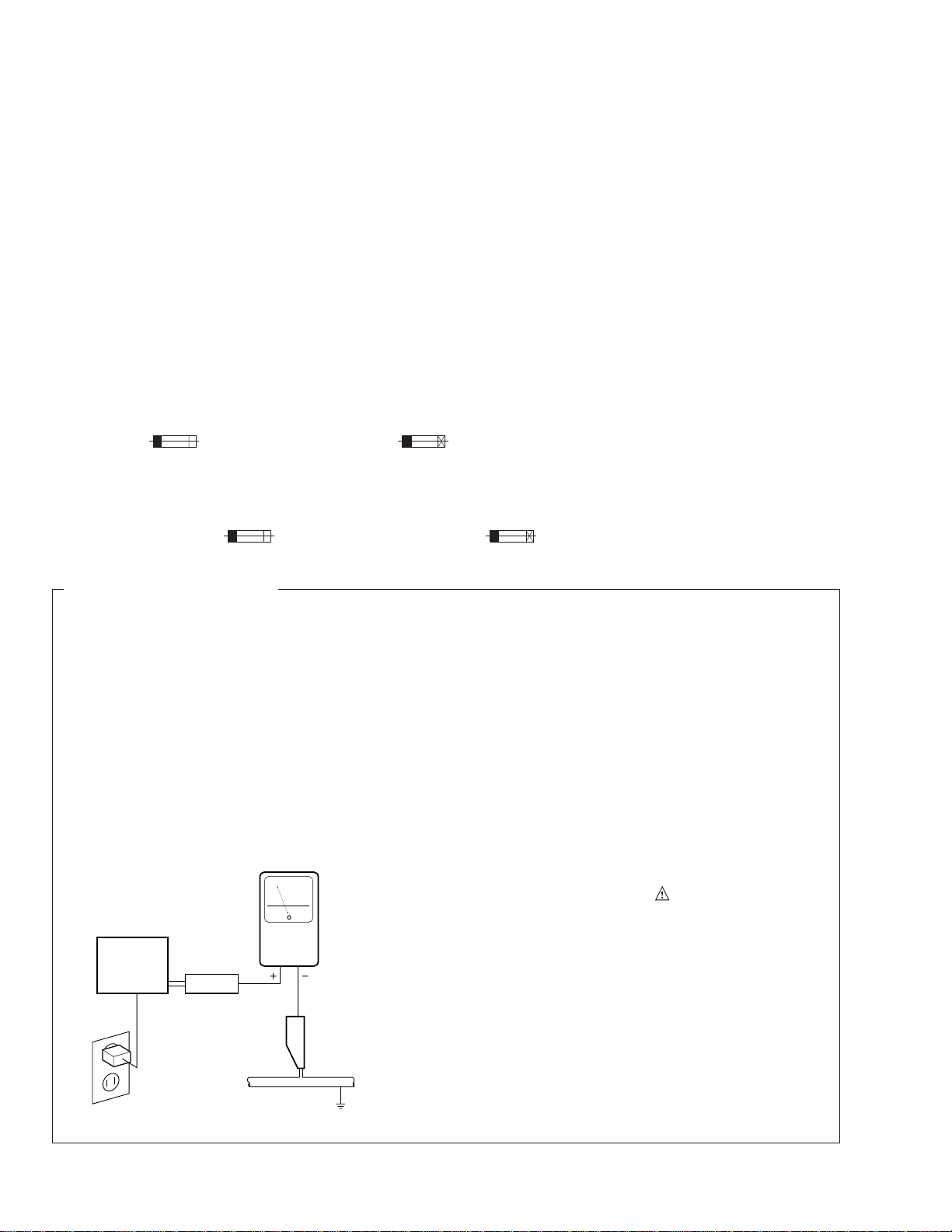
(FOR USA MODEL ONLY)
1. SAFETY PRECAUTIONS
The following check should be performed for the
continued protection of the customer and service
technician.
LEAKAGE CURRENT CHECK
Measure leakage current to a known earth ground
(water pipe, conduit, etc.) by connecting a leakage
current tester such as Simpson Model 229-2 or
equivalent between the earth ground and all exposed
metal parts of the appliance (input/output terminals,
screwheads, metal overlays, control shaft, etc.). Plug
the AC line cord of the appliance directly into a 120V
AC 60 Hz outlet and turn the AC power switch on. Any
current measured must not exceed 0.5 mA.
Reading should
not be above
0.5 mA
Earth ground
Device
under
test
Also test with plug
reversed
(Using AC adapter
plug as required)
Leakage
current
tester
Test all exposed
metal surfaces
AC Leakage Test
ANY MEASUREMENTS NOT WITHIN THE LIMITS
OUTLINED ABOVE ARE INDICATIVE OF A POTENTIAL SHOCK HAZARD AND MUST BE CORRECTED BEFORE RETURNING THE APPLIANCE
TO THE CUSTOMER.
2. PRODUCT SAFETY NOTICE
Many electrical and mechanical parts in the appliance have special safety related characteristics. These
are often not evident from visual inspection nor the
protection afforded by them necessarily can be obtained by using replacement components rated for
voltage, wattage , etc. Replacement parts which have
these special safety characteristics are identified in
this Service Manual.
Electrical components having such features are
identified by marking with a
on the parts list in this Service Manual.
The use of a substitute replacement component which
does not have the same safety characteristics as the
PIONEER recommended replacement one, shown in
the parts list in this Service Manual, may create shock,
fire, or other hazards.
Product Safety is continuously under review and
new instructions are issued from time to time. For
the latest information, always consult the current
PIONEER Service Manual. A subscription to, or additional copies of, PIONEER Service Manual may be
obtained at a nominal charge from PIONEER.
on the schematics and
2
Page 3

HTV-A1
3
Page 4
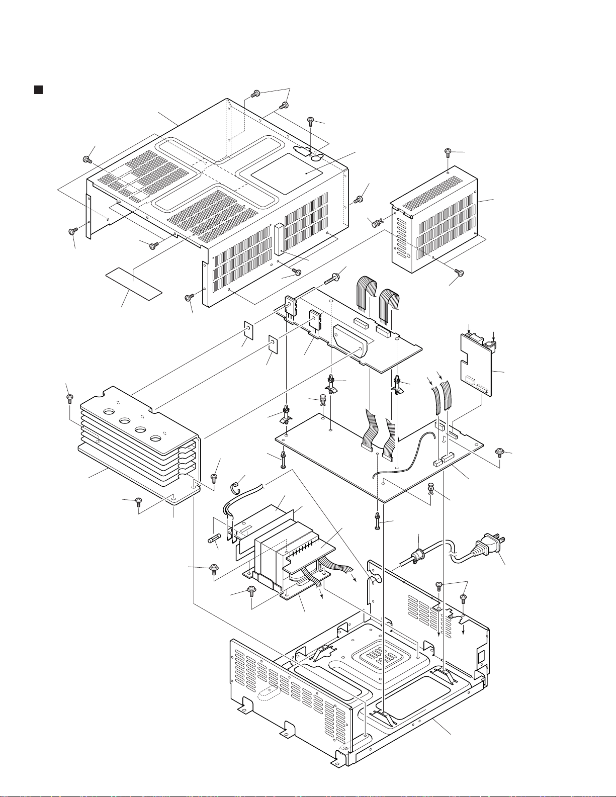
HTV-A1
2. EXPLODED VIEWS AND PARTS LIST
EXTERIOR
23
23
23
20
23
19
23
16
16
23
23
23
26
23
9
24
2
9
21
18
18
D
C
23
23
14
B
A
5
11
23
22
23
7
22
12
18
15
25
3
13
4
15
17
1
9
8
23
D
C
6
A
B
10
4
Page 5

NOTES : Parts marked by “ NSP ” are generally unavailable because they are not in our Master Spare Parts List.
The mark found on some component parts indicates the importance of the safety factor of the part.
Therefore, when replacing, be sure to use parts of identical designation.
Screw adjacent to mark on the product are used for disassembly.
EXTERIOR PARTS LIST
Mark No. Description Part No.
1 AFPS ASSY AWU7073
2 PAMP ASSY AWU7074
3 PT PRI ASSY AWU7075
4 PT SEC ASSY AWU7076
5 JACK ASSY AWU7077
6 Power Transformer (T1) ATS7212
7 Fuse (5A, FU1) REK1083
8 AC Power Cord PDG1057
9 Push Rivet AEC7149
NSP 10 Chassis ANA7076
NSP 11 Heat Sink ANH7076
12 Binder ZCA-SKB90BK
13 Barrier AEC7135
14 Heat Protector AEC7136
15 Mini Card Spacer AEC7143
HTV-A1
16 Mica Sheet AEE7010
17 Strain Relief CM-22C
NSP 18 PCB Holder PNW2174
19 Bonnet Case AZN7709
20 65 Label ORW1069
21 Screw ABA-258
22 Screw ASZ40P060FMC
23 Screw BBZ30P080FMC
24 Cushion AEB7123
25 Screw IBZ30P080FMC
NSP 26 Name Label AAX7637
5
Page 6
1
HTV-A1
3. SCHEMATIC DIAGRAM
3.1 OVERALL CONNECTIONS
A
B
23
PAMP ASSY
D
(AWU7074)
4
E
JACK ASSY
(AWU7077)
C
D
AFPS ASSY
A
(AWU7073)
6
1234
Page 7
5
678
HTV-A1
Note : When ordering service parts, be sure to refer to "EXPLODED VIEWS and P AR TS LIST" or "PCB PAR TS LIST".
A
B
B
PT SEC ASSY
(AWU7076)
AC 120V
60 Hz
AC POWER CORD
PDG1057
T1
POWER TRANSFORMER
ATS7212
C
C
PT PRI ASSY
(AWU7075)
D
7
5
6
7
8
Page 8
1
•
23
HTV-A1
3.2 AFPS, PT SEC AND PT PRI ASSEMBLIES
4
SIGNAL ROUTE
: AUDIO SIGNAL (L ch)
: AUDIO SIGNAL (SW ch)
A
BALANCED IN
E-VOLUME & TONE CONTROL, SUBWOOFER LEVEL
E
CN1105
1
2
+9.0
B
+4.5
(VREF)
I / O EXPANDER
Q1003, Q1004 :
AC RELAY DRIVER
0.0
3
+0.7
0.0
C
0.0
0.0
LPF 180Hz
L / R MIX
D
IC8001 (BU2092F)
No.
Pin Name
1 GNDD 0.0 V 0.0 V 0.0 V
2 DATA 5.0 V 5.0 V 5.0 V
3 CLK 0.0 V 0.0 V 0.0 V
4 LCK 0.0 V 0.0 V 0.0 V
5 PWON 5.1 V 0.0 V 0.0 V
6 SPRY 4.7 V 0.0 V 0.0 V
7 ACRY 5.1 V 0.0 V 0.0 V
8 MUTE 0.0 V 5.1 V 0.0 V
17 OE 0.0 V 0.0 V 0.0 V
18 VDD 5.1 V 5.1 V 5.1 V
STAND BY
ON MUTE
8
A
1234
Page 9
5
CAUTION : FOR CONTINUED PROTECTION AGAINST RISK OF FIRE,
REPLACE ONLY WITH SAME TYPE NO. 4911.25 MFD, BY
LITTELFUSE INK. FOR IC101 AND IC102(AEK7010).
CAUTION : FOR CONTINUED PROTECTION AGAINST RISK OF FIRE,
REPLACE ONLY WITH SAME TYPE NO. 491001 MFD, BY
LITTELFUSE INK. FOR IC103(AEK7009).
678
CAUTION : FOR CONTINUED PROTECTION AGAINST RISK OF FIRE,
REPLACE ONLY WITH SAME TYPE NO. 491010 MFD, BY
LITTELFUSE INK. FOR IC110 AND IC111(AEK7022).
CAUTION : FOR CONTINUED PROTECTION AGAINST RISK OF FIRE,
REPLACE ONLY WITH SAME TYPE NO. 491.250 MFD, BY
LITTELFUSE INK. FOR IC121 AND IC122(AEK7002).
HTV-A1
L
BUFFER AMP
HPF 180Hz
AFPS ASSY
A
(AWU7073)
A
D
CN1101
40Hz +9.5dB
HPF
D
CN1102
B
0.0
4700/63 ACH7007
ACH7007
4700/63
–17.9
+35.1
Q1001, Q1002 :
PROTECTION (SPEAKER)
RELAY DRIVER
+44.1
+35.1
–44.1
+17.7
B
T 1 : POWER TRANSFORMER
ATS7212
AC POWER CORD
PDG1057
5A/125V
FU 1 : REK1083
C
AC 120V
60 Hz
E
CN1104
C
D
POWER SUPPLY
• NOTE FOR FUSE REPLACEMENT
CAUTION -
FOR CONTINUED PROTECTION AGAINST RISK OF FIRE,
REPLACE WITH SAME TYPE AND RATINGS ONLY.
5
PT SEC ASSY
(AWU7076)
6
7
PT PRI ASSY
(AWU7075)
A
B C
9
8
Page 10

1
T
S
HTV-A1
3.3 PAMP ASSY
23
4
A
+35.0
–35.0
FRONT ch
POWER AMPLIFIER
+34.0
S
A
J1001
1.2k
1.2k
Q1301,
Q1302 :
OVER LOAD
B
DETECTOR
–34.0
A
J1002
+12.0
C
–11.7
Q1111 :
MUTE
4
D
5
1.1k
R1110
68
6
7
–43.9
+43.9
SW ch DI
10
1234
Page 11

5
678
HTV-A1
1.2k
STK407-040B
CAUTION : FOR CONTINUED PROTECTION AGAINST RISK OF FIRE,
REPLACE ONLY WITH SAME TYPE NO. 491.500 MFD, BY
LITTELFUSE INK. FOR IC1201 (AEK7005).
Q1201, Q1202 : MUTE
PROTECTION CIRCUIT
SIGNAL ROUTE
PAMP ASSY
D
(AWU7074)
A
: AUDIO SIGNAL (L ch)
: AUDIO SIGNAL (SW ch)
B
2SC5198
2SA1941
–44.0
SW ch DISCRETE POWER AMP
Q1307,
Q1308 :
DC DETECTOR
OVER LOAD
DETECTOR
C
D
11
5
6
7
8
Page 12

HTV -A1
Waveforms
Note: The encircled numbers denote measuring
point in the schematic diagram.
IC6001-Pin1 (DATA) 0.5 V/div 1 mS/sec
1
IC6001-Pin42 (CLK) 0.5 V/div 1 mS/sec
2
2
1
Measurement condition : volume Min =1
IC8001-Pin4 (LCK) 0.5 V/div 1 mS/sec
3
IC6001-Pin42 (CLK) 0.5 V/div 1 mS/sec
1
3
1
GND
GND
GND
GND
Q1109-Base 20 mV/div 5 mS/sec
5
Measurement condition :
SW ch output signal f =100Hz, 1W
Q1105-Collector 0.5 V/div 5 mS/sec
6
GND
GND
Measurement condition : volume Min =1
Q1110-Emitter 50 mV/div 5 mS/sec
4
Measurement condition :
SW ch output signal f =100Hz, 1W
GND
Measurement condition :
SW ch output signal f =100Hz, 1W
Q1106-Collector 0.5 V/div 5 mS/sec
7
Measurement condition :
SW ch output signal f =100Hz, 1W
GND
12
Page 13

1
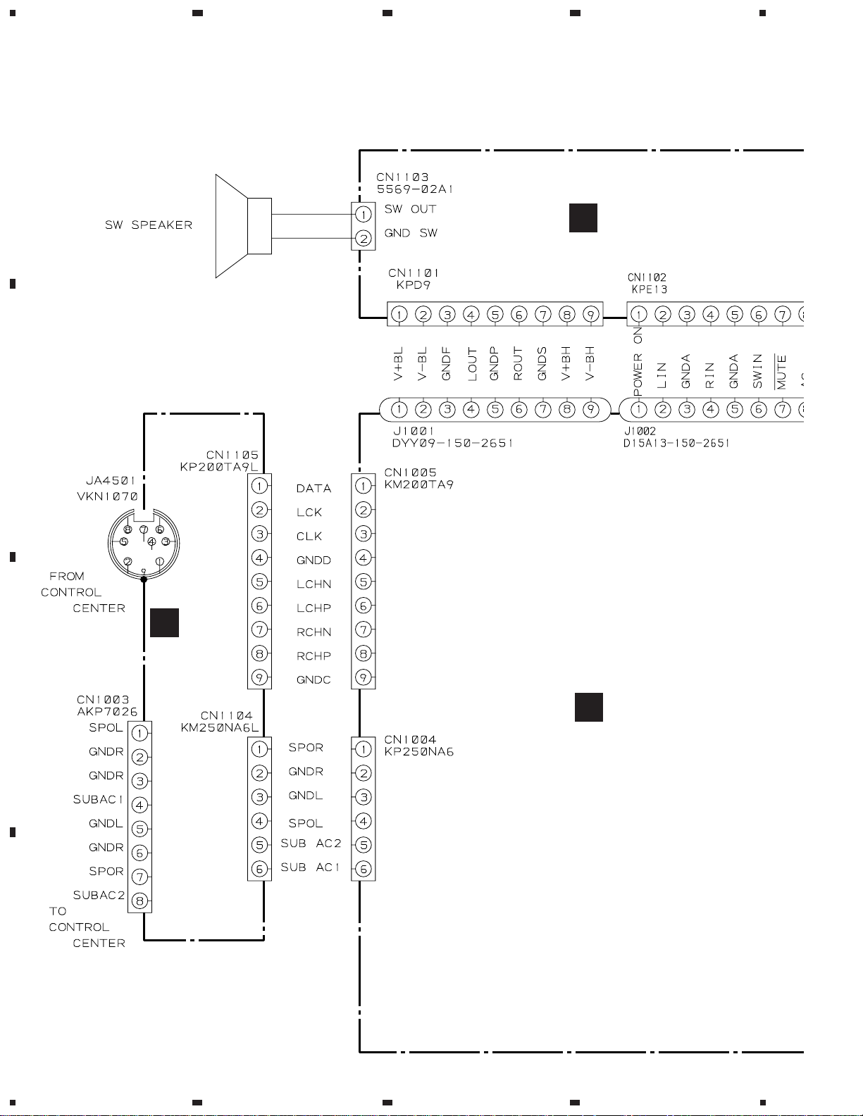
3.4 JACK ASSY
234
HTV -A1
A
JACK ASSY
E
(AWU7077)
A
CN1005
B
TO CONTROL CENTER HTV-C1
1
A
CN1004
SIGNAL ROUTE
: AUDIO SIGNAL (L ch)
13
2
3
4
C
D
Page 14

1
23
HTV -A1
4. PCB CONNECTION DIAGRAM
A
NOTE FOR PCB DIAGRAMS :
1. Part numbers in PCB diagrams match those in the schematic
diagrams.
2. A comparison between the main parts of PCB and schematic
diagrams is shown below.
Symbol In PCB
Diagrams
BCE
BCE
D
Symbol In Schematic
Diagrams
BCEBCE
BCE
DGGSS
BCE
DGS
Part Name
Transistor
Transistor
with resistor
Field effect
transistor
4
3. The parts mounted on this PCB include all necessary parts for
several destinations.
For further information for respective destinations, be sure to
check with the schematic diagram.
4. View point of PCB diagrams.
Connector
Capacitor
SIDE A
P.C.Board
Chip Part
SIDE B
B
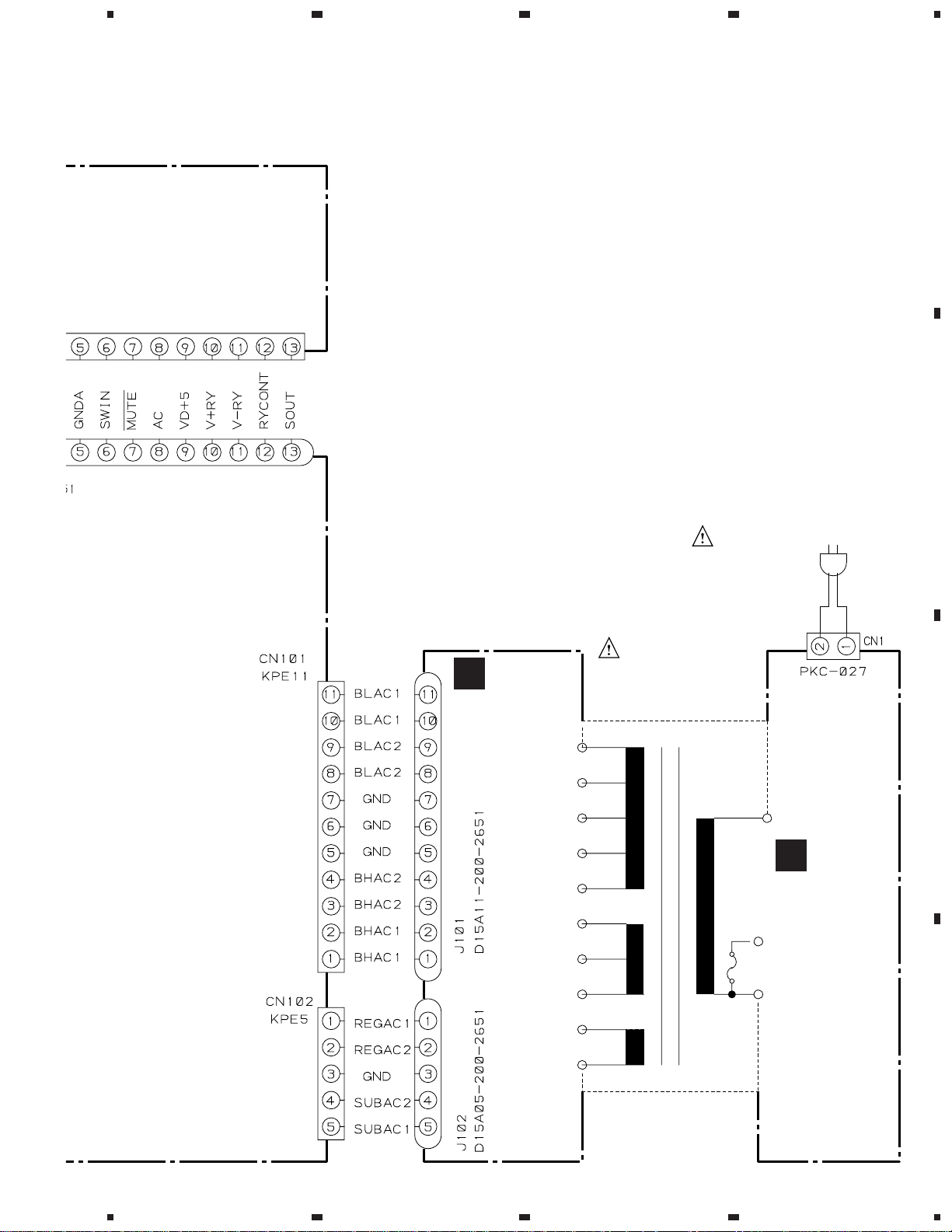
4.1 PT SEC ASSEMBLY
C
Resistor array
3-terminal
regulator
B
PT SEC ASSY
POWER TRANSFORMER
A
CN101
A
SIDE A
IC110,IC101
IC111,IC103,IC102
(ANP7253-C)
CN102
SIDE B
D
(ANP7253-C)
14
1234
Page 15

1
234
4.2 PT PRI AND JACK ASSEMBLIES
C
PT PRI ASSY
POWER TRANSFORMER
NEUTRAL
HTV -A1
A
SIDE A
AC POWER CORD
TO
CONTROL CENTER
HTV-C1
FROM
CONTROL CENTER
HTV-C1
LIVE
E
JACK ASSY
B
(ANP7253-C)
C
A
CN1004
A
CN1005
(ANP7253-C)
D
15
1
2
3
4
Page 16

1
B
23
HTV -A1
4.3 AFPS AND PAMP ASSEMBLIES
4
SIDE A
A
Q1102,Q1309
Q1107,Q1106
B
Q1103,Q1109,Q1110
Q1101,Q1105,Q1108,Q1111
TO SW SPEAKER
Q1104
Q1112
D
PAMP ASSY
E
CN1104
E
CN1105
Q1310,Q1306,Q1303
Q1304,Q1305
Q1202
C
IC1201
Q1201
Q1204
IC1101
Q1203
Q1208,Q1307
D
Q1302
Q1301
(ANP7253-C)
16
1234
Page 17

5
678
HTV -A1
B
J101
B
J102
SIDE A
A
AFPS ASSY
IC105,Q102
IC121,Q104,Q103
IC122
Q105
IC106
Q101
A
B
4
5
Q6051,Q6052
C
Q1005
Q1002
Q1004
Q301
Q303
Q302
(ANP7253-C)
D
17
5
6
7
8
Page 18

A
HTV -A1
IC4502,IC4501
IC4503
1
A
AFPS ASSY
23
4
B
C
IC6001
Q106
SIDE B
IC6031,6501
IC6701,IC7101
Q1001
D
Q1003
IC8001,Q8001
(ANP7253-C)
18
1234
Page 19

5
678
HTV -A1
D
PAMP ASSY
SIDE B
A
B
C
D
(ANP7253-C)
19
5
6
7
8
Page 20

HTV-A1
5. PCB PARTS LIST
NOTES :
Parts marked by “ NSP ” are generally unavailable because they are not in our Master Spare Parts List.
The mark found on some component parts indicates the importance of the safety factor of the part.
Therefore, when replacing, be sure to use parts of identical designation.
When ordering resistors, first convert resistance values into code form as shown in the following examples.
Ex. 1 When there are 2 effective digits (any digit apart from 0), such as 560 ohm and 47k ohm (tolerance is shown by
J = 5%, and K = 10%).
1
560 Ω = 56 × 10
47k Ω = 47 × 10
= 561................................................... RD1/4PU 5 6 1 J
3
= 473 .................................................. RD1/4PU 4 7 3 J
0.5 Ω = R50 ...................................................................... RN2H Â 5 0 K
1 Ω = 1R0 ......................................................................... RS1P 1 Â 0 K
Ex. 2 When there are 3 effective digits (such as in high precision metal film resistors).
5.62k Ω = 562 × 10 1 = 5621 ........................................... RN1/4PC 5 6 2 1 F
Mark No. Description Part No.
LIST OF PCB ASSEMBLIES
MOTHER ASSY AWM7368
AFPS ASSY AWU7073
PAMP ASSY AWU7074
PT PRI ASSY AWU7075
PT SEC ASSY AWU7076
JACK ASSY AWU7077
A
AFPS ASSY
SEMICONDUCTORS
IC121, IC122 (250mA/125V) AEK7002
IC8001 BU2092F
IC6001 M62419FP
IC4501–IC4503, IC6031, IC6501, IC6701 NJM4558MD
IC7101 NJM4558MD
IC105 NJM7812FA
IC106 NJM7912FA
Q104 2SA933S
Q102 2SB1237X
Q1002, Q1005, Q103 2SC1740S
Q6051, Q6052 2SC1740S
Q101 2SD1858X
Q105 2SD1858X
Q1001, Q1003, Q106 DTA143EK
Q8001 DTC124EK
Q1004 DTC143ES
D103–D106 11ES2
D1001–D1004, D8001, D8002 1SS254
D101 D3SBA20 (B)
D102 D5SBA20 (B)
D6051 MTZJ10B
D8003 MTZJ2.7B
D107 MTZJ5.6B
D6001, D6002, D8004–D8006 MTZJ8.2B
RELAYS
RY1002 ASR7001
RY1001 ASR7009
CAPACITORS
C101, C102 (4700 µF/DC63V) ACH7007
C103, C104 (3300 µF/DC50V) ACH7056
Mark No. Description Part No.
C6013, C6014 CCSQCH470J50
C7102, C7103 CEANPR47M50
C6011, C6012, C6015–C6018 CEAT100M50
C6031, C6032, C6051, C6053 CEAT100M50
C6701, C6702, C7104, C7105, C8006 CEAT100M50
C6004 CEAT101M10
C6052 CEAT101M16
C105 CEAT102M25
C6054 CEAT221M10
C6503, C6504 CEAT2R2M50
C106 CEAT331M25
C107–C109, C111, C8001, C8007 CEAT470M25
C110, C6019, C6020 CEAT4R7M50
C8003–C8005 CKSQYB102K50
C6005, C6006 CKSQYB472K50
C6021, C6022, C6025, C6026 CKSQYB682K50
C6023, C6024 CKSQYB683K25
C4501–C4506, C6001, C6003, C8002 CKSQYF103Z50
C1001–C1004, C216, C217 CKSQYF104Z50
C6060 CKSQYF473Z50
C205–C208 CQMA223K2E
C6704 CQMBA104J50
C6501, C6502, C6703 CQMBA473J50
RESISTORS
R8004 RD1/2PM222J
R1001, R1002 RD1/4PM100J
R101 RD1/4PU182J
R102 RD1/4PU220J
R8005 RD1/4PU273J
R6051 RD1/4PU821J
R4505–R4512 RS1/10S1001F
R110 RS3LMF151J
Other Resistors RS1/10S J
OTHERS
CABLE HOLDER (9P) 51052-0900
CABLE HOLDER (13P) 51063-1305
J1002 JUMPER WIRE D15A13-150-2651
CN1005 9P PLUG KM200TA9
CN1004 SOCKET 6-P KP250NA6
CN101 CONNECTOR (11P) KPE11
CN102 CONNECTOR (5P) KPE5
KN101, KN102 EARTH METAL FITTING VNF1084
20
Page 21

HTV-A1
Mark No. Description Part No. Mark No. Description Part No.
PAMP ASSY
D
SEMICONDUCTORS
IC1201 (500mA/125V) AEK7005
IC1101 STK407-040B
Q1105 2SA1145
Q1104 2SA1837
Q1102 2SA1941 (P)
Q1203 2SA933S
Q1108 2SA970
Q1109, Q1110 2SA992
Q1107 2SC1740S
Q1301, Q1302, Q1307, Q1308 2SC1740S
Q1309 2SC2240
Q1106 2SC2705
Q1103 2SC4793
Q1101 2SC5198 (P)
Q1111, Q1201, Q1202 2SD2144S
Q1306, Q1310 DTA123JS
Q1112, Q1303 DTA143ES
Q1204 DTC124ES
Q1304, Q1305 DTC143ES
D1307, D1309 11ES2
D1101–D1103, D1301–D1304, D1308 1SS254
D1310–D1312, D1316 1SS254
R1109 RD1/4PM104J
R1110 RD1/4PM112J
R1125, R1215, R1216 RD1/4PMF100J
R1116–R1119 RD1/4PMF101J
R1112 RD1/4PMF680J
R1312 RD1/4PU222J
R1315 RD1/4PU821J
R1115 RF1/4PS101J
R1120–R1123 RF1/4PS4R7J
R1213, R1214 RS2LMFR22J
Other Resistors RS1/10S J
OTHERS
CN1103 2P CONNECTOR 5569-02A1
CN1101 9P JUMPER CONNECTOR KPD9
CN1102 CONNECTOR (13P) KPE13
PT PRI ASSY
C
CAPACITOR
C1 (10000pF/AC250V) ACG7020
OTHERS
H1, H2 FUSE CLIP AKR7001
COILS
L1201, L1202 (1 µH) ATH-133
L1101 (0.7 µH) ATH1004
RELAY
RY1101 ASR7001
CAPACITORS
C1107, C1108 CCCSL101K2H
C1104 CCCSL120K2H
C1106 CCCSL5R0C2H
C1207, C1208 CCSQSL3R0C50
C1103 CCSQSL681J50
C1105 CEANP101M50
C1306 CEANP2R2M50
C1100, C1101, C1205, C1206 CEAT100M50
C1209, C1210, C1304 CEAT100M50
C1111, C1303 CEAT101M10
C1211, C1212 CEAT101M50
C1120 CEAT220M50
C1305 CEAT221M10
C1213 CEAT330M50
C1307 CEAT470M25
C1201, C1202 CEYA1R0M50
C1203, C1204 CKSQYB152K50
C1102 CKSQYB223K50
C1109, C1110, C1219 CKSQYF104Z50
RESISTORS
R1124 (0.33 Ω) ACN7001
R1126 RD1/2PM100J
R1217, R1218 RD1/4LMF101J
PT SEC ASSY
B
SEMICONDUCTORS
IC103 (1A/125V) AEK7009
IC101, IC102 (1.25A/125V) AEK7010
IC110, IC111 (10A/125V) AEK7022
CAPACITORS
C123 (0.01 µF/DC100V) ACG7021
C121, C122 CKSQYF103Z50
OTHERS
CABLE HOLDER (5P) 51063-0505
J102 JUMPER WIRE D15A05-200-2651
J101 JUMPER WIRE D15A11-200-2651
JACK ASSY
E
CABLE HOLDER (11P) 51063-1105
SEMICONDUCTORS
D4501–D4506, D4508 MTZJ8.2B
CAPACITORS
C4601–C4606 CKCYF103Z50
OTHERS
CN1003 8P CONNECTOR AKP7026
CN1104 PLUG 6-P KM250NA6L
CN1105 9P SOCKET KP200TA9L
I/O JACK VKN1070
SCREW PLATE VNE1948
21
Page 22

HTV-A1
6. ADJUSTMENT
There is no information to be shown in this chapter.
7. GENERAL INFORMATION
7.1 IC
BU2092F (IC8001: AFPS ASSY)
Serial In/Parallel Out Driver
DD
V
OE
Q11
Q10
Q9
Q8
Q7
Q6
Q3
Q5
Q4
18 17 16 15 14 13 12 11 10
Output Buffer (Open Drain)
Control Circuit
12 bits Shift Register
12 bits Strage Register
123456789
Q0
Q1
Vss
DATA
LCK
CLOCK
Q2
M62419FP (IC6001: AFPS ASSY)
Electronic Volume Control with Tone Function
¶ The information shown in the list is basic information and may not
correspond exactly to that shown in the schematic diagrams.
Pin Function Block Diagram
No. Name I/O Description
1 Vss – GND
2 DATA I Serial data input
3 CLOCK I Shift lock for data ( )
4 LCK I Lutch clock for data ( )
Parallel data output (Nch Open Drain FET)
5Q0
||O
16 Q11
17 OE I Output enable (H: output, FET: OFF)
18 VDD – Power supply
Lutch Data L H
Output FET ON OFF
Block Diagram
CLOCK
CLOCK
I/F
DATA
DATA
VDD
SELECT OUT 2
DD
V
GND
SELECT OUT 1
VOL IN 2
LOUD IN 2
VOL IN 1
LOUD IN 1
SELECT 2 NF 2
SELECT 2 IN A
SELECT 2 IN B
–
+
+
–
–
+
+
–
SELECT 1 IN A
SELECT 2 NF 1
SELECT 1 IN B
SELECT 2 IN C
SELECT 2 IN D
ATTF OUT 2
SELECT 1 IN C
ATTF OUT 1
SELECT 1 IN D
ATTR OUT 2
TONE IN 2
+
–
–
+
TONE IN 1
ATTR OUT 1
TC 2 A
TC 1 A
TC 2 B
–
+
+
–
TC 1 B
TC 2 C
TC 1 C
TONE OUT 2
FADER IN 2
+
+
FADER IN 1
TONE OUT 1
REAR OUT 2
FRONT OUT 2
2242 41 40 39 38 37 36 35 34 33 32 31 30 29 28 27 26 25 24 23
+
–
–
Vref
–
–
+
211234567891011121314151617181920
REAR OUT 1
FRONT OUT 1
VREF
Vcc
Vcc
22
Page 23

Pin Function
HTV-A1
No. Name Description
1 DATA Control data input terminal.
Data are entered synchronized to CLOCK.
2 GND Ground terminal
3 SELECT OUT1 Output terminals of the input selector switch
4 VOL IN1 Input terminals of the volume control section
5 LOUD IN1 Frequency characteristic setting terminal of
the loudness section
6 SELECT2 NF1 Each input gain is adjusted by the resistor
connected between this terminal and the
SELECT OUT terminal and the resistor added
between IN A and IN D.
7 SELECT1 IN A Input terminal for channel 1 of the input selector
switch section
8 SELECT1 IN B
9 SELECT1 IN C
10 SELECT1 IN D
11 ATTF OUT1 Output terminals of the volume control section
(initial stage). Connect by C connection to the
VREF terminal 22 for reduction of the switching
noise.
12 ATTR OUT1 Output terminals of the volume control section
(last stage)
13 TONE IN1 Input terminals of the tone control section
14 TC1 A Frequency characteristic setting terminals of
the tone control section for channel 1
15 TC1 B
No. Name Description
24 REAR OUT2 Output terminals of the fader volume control
section (rear)
25 FADER IN2 Input terminals of the fader volume control section
26 TONE OUT2 Output terminals of the tone control section
27 TC2 C Frequency characteristic setting terminals of
the tone control section for channel 2
28 TC2 B
29 TC2 A
30 TONE IN2 Input terminals of the tone control section
31 ATTR OUT2 Output terminals of the volume control section
(last stage)
32 ATTF OUT2 Output terminals of the volume control section
(initial stage). Connect by C connection to the
VREF terminal 22 for reduction of the switching
noise.
33 SELECT2 IN D Input terminal for channel 2 of the input selector
switch section
34 SELECT2 IN C
35 SELECT2 IN B
36 SELECT2 IN A
37 SELECT2 NF2 Each input gain is adjusted by the resistor
connected between this terminal and the
SELECT OUT terminal and the resistor added
between IN A and IN D.
38 LOUD IN2 Frequency characteristic setting terminal of
the loudness section
16 TC1 C
17 TONE OUT1 Output terminals of the tone control section
18 FADER IN1 Input terminals of the fader volume control section
19 REAR OUT1 Output terminals of the fader volume control
section (rear)
20 FRONT OUT1 Output terminals of the fader volume control
section (front)
21 Vcc Analog power supply terminal
22 DATA IC signal ground. Impress 1/2 VCC.
23 FRONT OUT2 Output terminals of the fader volume control
section (front)
39 VOL IN2 Input terminals of the volume control section
40 SELECT OUT1 Output terminals of the input selector switch
41 VDD Digital power supply terminal
42 CLOCK Clock input terminal for serial data transfer
23
Page 24

HTV-A1
Screw A
Screw A
PAMP Assy
Screw A
PCB Holder
PCB Holder
PCB Holder
Heat Sink
7.2 DIAGNOSIS
Diagnosis Method for the Power Amplifier section (PAMP Assy)
(1) Remove the three screws A fixing the Heat sink.
(2) Remove the three PCB Holders and rotate as shown in the Fig 1.
D
Fig. 1
PAMP ASSY
SIDE B
Heat Sink
PAMP Assy
Fig. 2
24
Page 25

Diagnosis Method for the AFPS Assy
(1) Remove the three screws A fixing the Heat sink.
(2) Remove the three PCB Holders and then remove the Heat
sink. (Refer to Fig.1)
(3) Remove the screw B, remove the two screws C, remove
the two push rivets D, and then remove the AFPS assy.
(Refer to Fig. 3)
(4) Short-circuit KN101 of the AFPS assy and KN1001 of the
JACK assy.
(5) Short-circuit all test terminals of the AFPS assy (SPRY,
ACRY, PWON) to GNDD.
(6) Remove C6031, enter an audio signal to the AL4 (Lch in)
terminal, and analyze the AFPS assy. (Refer to Fig. 4)
HTV-A1
Push Rivet D
Screw C
JACK Assy
Short-circuit SPRY, ACRY and
PWON terminals to GNDD.
Enter an audio signal
Remove C6031
Screw B
Push Rivet D
AFPS Assy
Fig. 3
KN1001
JACK Assy
A
AFPS ASSY
Fig. 4
SIDE A
KN101
AFPS Assy
25
Page 26

HTV -A1
7.3 BLOCK DIAGRAM
CONTROL CENTER
HTV-C1
(Refer to the service manual RRV1960 HTV-C1/AUXJ, ACXJ)
26
Page 27

AMPLIFIER
HTV-A1
HTV -A1
AC120V
60Hz
AC POWER CORD
27
Page 28

HTV-A1
8. PANEL FACILITIES AND SPECIFICATIONS
SPECIFICATIONS
HTV-1
Amplifier Section
[Front left and right channels]
Continuous average power output of 30
watts* per channel, min., at 8 ohms, from 180
Hz to 15,000 Hz with no more than 1 %** total
harmonic distortion.
[Subwoofer channel]
Continuous average power output of 60
watts* , min., at 8 ohms, from 40 Hz to 180
Hz with no more than 1 %** total harmonic
distortion.
* Measured pursuant to the Federal Trade Commission’s Trade
Regulation rule on Power Output Claims for Amplifiers.
** Measured by Audio Spectrum Analyzer.
Input (Sensitivity/Impedance)
INPUT 1, 2 ........................................................... 200 mV/22 kΩ
Speaker Section
Front L/R ............................................................ 8.7 cm cone type
Subwoofer ......................................................... 20 cm cone type
Miscellaneous
Power Requirements .......................................... AC 120 V, 60 Hz
Power Consumption .......................................................... 150 W
Dimensions
Control center ....................... 610 (W) × 110 (H) × 166 (D) mm
Powered subwoofer ............. 364 (W) × 360 (H) × 371 (D) mm
Weight (without package)
Control center ................................................. 3.8 kg (8 lb 6 oz)
Powered subwoofer ................................. 13.5 kg (29 lb 12 oz)
Furnished Parts (HTV-C1)
System cable A ............................................................................ 1
System cable B ............................................................................ 1
Audio cord ................................................................................... 1
Mount kit ...................................................................................... 1
Dry Cell Batteries (AA/R6P) ........................................................ 2
Remote Control Unit ................................................................... 1
Operating Instructions ................................................................ 1
Warranty card .............................................................................. 1
24-3/16 (W) × 4-5/16 (H) × 6-9/16 (D) in
14-5/16 (W) × 14-3/16 (H) × 14-5/8 (D) in
NOTE:
Specifications and the design are subject to possible modifications
without notice, due to improvements.
Manufactured under license from the Dolby Laboratories.
DOLBY and the double-D symbol
Laboratories.
28
are trademarks of Dolby
 Loading...