

Page 1
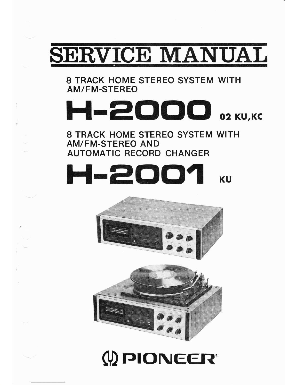
SERVICE
MANUAL
8
TRACK
HOME
STEREO SYSTEM
WITH
AM IFM.STEREO
Hr?(]OO
o2KU,Kc
8
TRACK
HOME
STEREO
SYSTEM
WITH
AM/FM.STEREO
AND
AUTOMATIC RECORD
CHANGER
HI?oO1
KU
()rrloNeeltR'
Page 2
CONTENTS
1. SPECIF|CAT|ONS
2
2. PARTS
LOCATION
2.'l H-2000
3
2.2 H-2001
4
3. CIRCUITDESCR|PT|ON....
5-6
4. DISASSEMBLY..
7
5. ADJUSTMENT
5.1 FM
lF Adjustment . .
5.2 FM
Tracking
Adjustment
5.3 MPX
Separation Adjustment . . . .
5.4 AM Tracking
Adjustment
5.5 Tape
Mechanism
Adjustment . . .
12-
DIAL
STRINGING
CI RCUIT
DIAGRAM
SECTION
7.1
H-2000
Schematic
Circuit Diagram ....
.
14- 15
7.2 H-2001
SchematicCircuitDiagram
..... 18- 19
7.3 TunerUnit(CWE-083-A)
....17,20-22
7.4
Equalizer
Unit
(CWK-079-0)
. .
.
.
23- 24
7.5
Volume
Control Unit
(CWK-080-0)
.
..
. .
25- 26
7.6 Tone
Control
Unit
(CWK-081-0)
.
27
-
28
7.7
Amplifier
Unit
(CWK-082-A).
. . .
29
-
31
7"8 PowerSupplyUnit
(CWR-044-O1
..
.....32-33
7.9 Miscellaneous
8.
EXPLODED
VIEW
8.1
Cabinet
8.2 Chassis
..37-39
8.3 Mechanism
.....40-42
9. PACKING
METHOD
9.1
H-2000
9.2 H-2001
8
I
10
11
13
13
6.
7.
34
35-36
43
44
Page 3
H-2000
H 2001
1
.
SPECIFICATIONS
SEM
I
CONDUCTORS
1 FET,
18 Transistors,
16 Diodes
POWER
SUPPLY
SECTION
POWER
SOURCE
AC
12OV,5OI6OHZ
POWER
CONSUMPTION
Less than
60W
(70W
H
2001)
AUXILIARY
OUTLET
150 Watts
Unswitched
(H
2000
Onty)
AMPLIFIER
SECTION
OUTPUT POWER
8W
(TJl.D.5%,8s))
PHONO
INPUT
150mV, 1MS)
FREOUENCY
RESPONSE
20
-
15,000H2
(lVlain
Amplif
ier
lnput)
SIGNAL
TO NOISE
RATIO
.
. .
.
.
More than 45dB
OUTPUT
IMPEDANCE
8A
TAPE
SECTION
CARTR IDGE
Any
8-Track Cartridge
TAPE
SPEED
9.Scm/sec
(3-3/4inlsec)
WOW
AND FLUTTER
Less than 0.25%
(WRMS)
CROSSTALK
More than 40dB
SIGNAL
TO NOISE
RATIO . . . . .
More than 40dB
FM
AND MPX
SECTION
FREOUENCY
RANGE
88.0
-
108MHz
SENSITIVITY....
10pV(lHF)
IMAGE
REJECTION
More than
38dB
SIGNAL TO NOISE
RATIO
More than 45dB
CHANNE
L
SEPARATION . .
More
than
24dB
(at
i kHz)
ANTENNA IIV]PEDANCE
3OOQ
AM
SECTION
FREOUENCY
RANGE
525
-
1,6O5KHZ
SENSITIVITY ....
10pV
(tHF)
IMAGE
REJECTION
More
than 45dB
SIGNAL TO NOISE
RATIO
More than
40dB
ANTENNA
Built-ln Ferrite
Bar
Antenna
DIMENSIONS
(WX
H X D)
H
2000
475x120x298mm
(1811116x423132x1123132in1
H2-OO1
476x236x381mm
(18314
x9-3/8x
15in)
WEIGHT
H-2000
5.7ks
(12.6tbs),
H 200i
9.0
kg
(21.1tbs)
RECORD
PLAYER
SECTION
(H-2001
Only)
MODEL
BSR
C141R-1 Automatic
Record Changer
RECORD
SIZE
.
7, 10, 12iN
SPEED
33,45, 78rpm
RECORD
HOLDING
CAPACITY
..
Up to 8 Same
Size Records
WOW AND FLUTTER
Less than 0.2%
CARTR IDGE
Ceramic
Stereo
Cartridge, Sapphire/Diamond
Stylus
SPEAKER
SECTION
SPEAKER
H 2000
j6cml6-1l2lx2
H-2001
Woofer
20cm
(8in),
Tweeter
7.7cm
(3in)Two
Way x
2
IIV]PEDANCE
8f,2
DIMENSIoNS
(wx
H
x
D) .......
H-2000
3o4x444x
190mm
(12x17-112x7-1l2in\x2
H 2001 343x
546x
263mm
(13112x21
1l2x
10-11
l32in\x2
H 2000 4.8ks
(10.61bs)
x
2, H-2001
8.2kq
(18.1
tbs) x
2
WEIGHT
Page 4
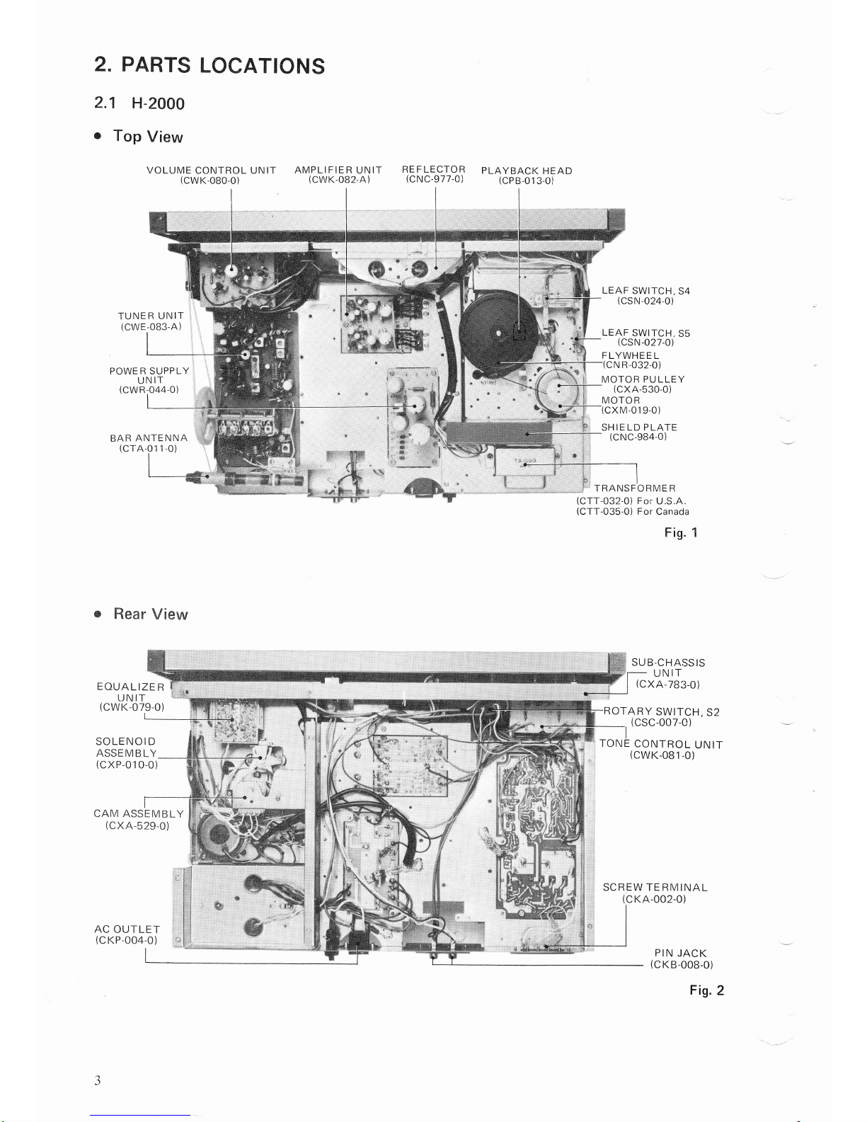
2.
PARTS
LOCATIONS
2.1
H-2000
o
Top
View
VOLUME
CONTROL UNIT
AMPLIFIER UNIT
(cwK-080-0)
(cwK-082-A)
RE F LECTOR
PLAYBACK
HEAD
(CNC-977-0)
(CpB-g13-0)
TUNER
UNIT
(CW
E.OB3-A
)
POWE R SUPP
LY
UN
IT
(cw
R
-044-0)
BAR
ANTENNA
(crA-O1
1-0)
&
Rear
View
EOUALIZER
UN IT
(cwK-079-0)
SCLENOID
ASSE
M
B LY
(cxP-01
0-0)
CAM ASSEMBLY
(c
x
A-5
29-0
)
AC
OUTLET
(c
KP-004-0
)
fl$.$-$ffi
T
RA
NS'IO *
M E
R
LEAF
SWITCH,
54
(csN
-024-ol
LEAF
SWITCH,
55
(csN
-o21-ol
FLYWHEEL
(cN
R-032-0)
MOTOR
PULLEY
(cxA-530-0)
MOTO R
(cxM-019-0)
SHIELD
PLATE
(c
NC-984-0
)
(CTT-032-0)
For-
U.S.A.
(CTT-035-0)
For
Canada
i;i':,:,,,...'.,',,,.,.,.,.,.,i;.,.i..i.,.:;:,::::.i:i.:::::::,::,:,.:.:..:.,.:.::t::::::',:,:,:,:i:'::,:,:i:::::::...t:t:it.t.t
,.
.,.,,,
', i ,1
.,
,:,,,,',,,,,,,,iii',;iil:l
l ll.,,,
i:,:,,,:,':,:
ii
:,:,:,:,:,i
,,,,:::,:':
i:
:i :,:,:,:,:,1 :,:,:,:l:::l
:,1 :iiii
Fig.
1
SUB-CHASSIS
UN
IT
(c
x A-
783-0
)
ROTARY
SWITCH,
52
(csc-00
7-0
)
TONE
CONTROL
UNIT
(cwK-081
-0)
SCREW TE RM
INAL
(c
KA-002-0)
PIN
JACK
(c
K B-008-0
)
Fig.2
Page 5
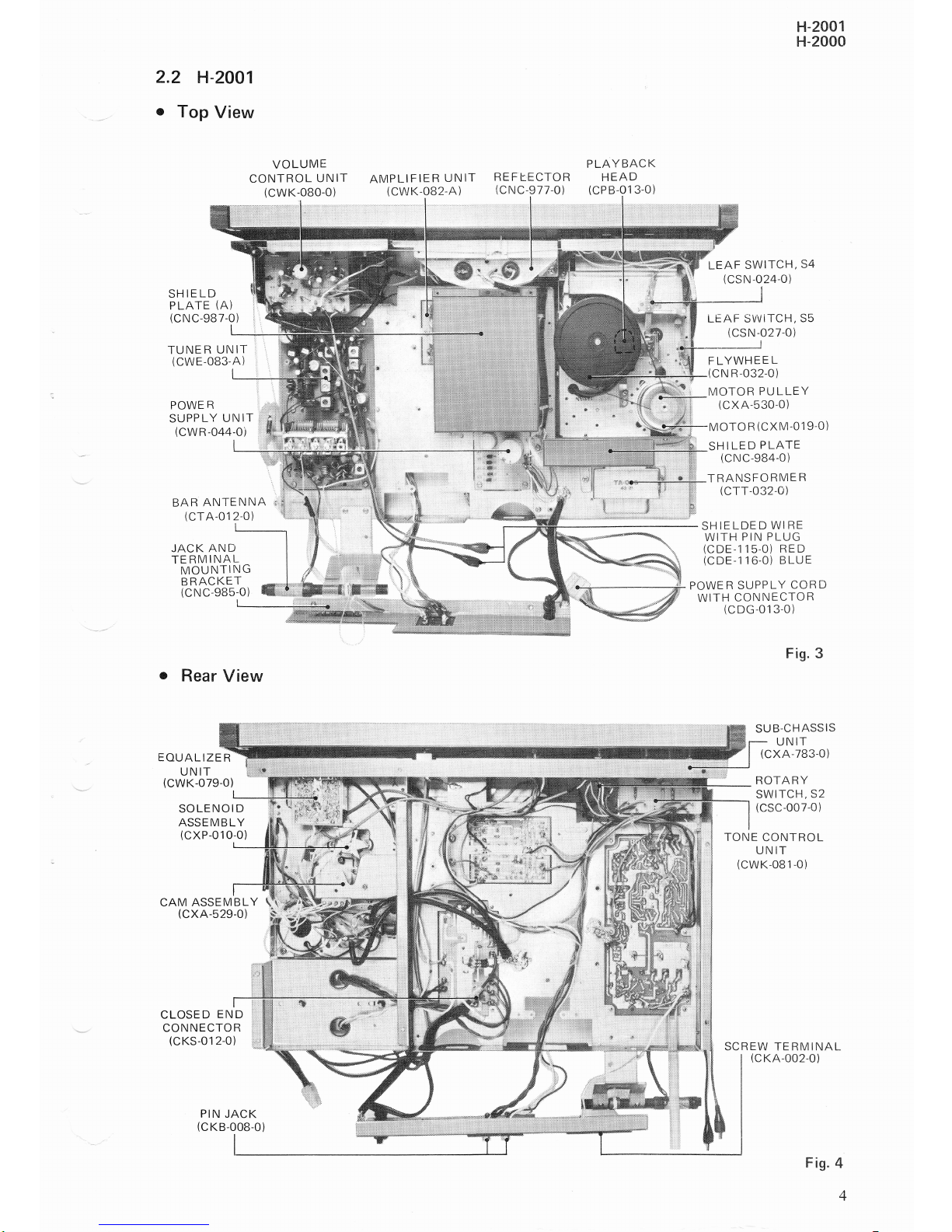
2.2
H-2001
o
Top
View
SHIELD
P
LATE
(A)
(c
N
c-98
7-0)
TUNER
UNIT
(CW
E-OB3-A )
POWE
R
SUPP
LY UN
tT
(cw
R-044-0)
VOLUM
E
CONTROL
UN
IT
(cwK-080-0)
ATVIPLIFIER
UNIT
(cwK-082-A)
PLAYBACK
REFhECTOR
HEAD
(cNC-917-O)
(CpB-013-0)
**-""t"r"w@+tU*
.\
\
da
H-2001
H-2000
Fis"
4
4
BAR
ANTENNA
(crA-012-ol
JACK AND
TE
RM
I NAL
MOUNTING
BRACKET
(c
N c-985-0)
Rear
View
EQUALIZER
UN IT
(cwK-079-0)
SOLENOID
ASSE M B LY
(cxP-01
0-0)
CAM
ASSEMBLY
(cxA-529-0
)
CLOSED
END
CONNECTOR
(c
KS
-0
12-Ol
PIN
JACK
(c
K B-008-0
)
LEAF
SWITCH,
54
(csN
-o24-o\
LEAF
SVVITCH,
55
(csN
-o2t
ol
FLYWHEEL
(cN
R-032-0)
TVIOTOR
PULLEY
(c
x A-5 30-0
)
MOTO
R
(CXM-019-0)
SHILED
PLATE
(c
N
c-984-0
)
TRANSFORMER
(crr-0
32-0
)
SH
IE LDE
D
WI RE
WITH
PIN PLUG
(CDE-1i5.0)
RED
(cor-1
16-0) BLUE
POWER
SUPPLY
CORD
WITH
CON
N
ECTO
R
(cDG-013-0)
Fig. 3
SU
B-C
H ASS
IS
UN
IT
(c
x
A-783-0
)
ROTA
RY
SWITCH,
52
(csc-00
7-0
)
TONE
CONTROL
UN
IT
(cwK-081
-0)
SCREW
TERMINAL
(c
KA-002-0)
Page 6
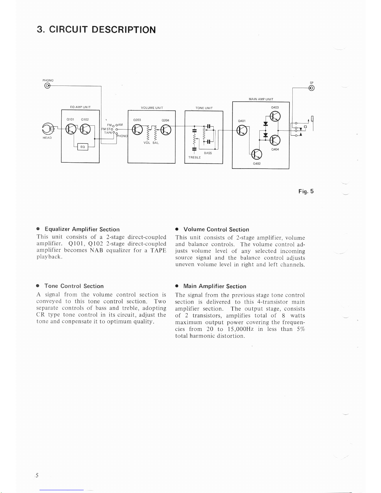
3. CIRCUIT
DESCRIPTION
Fis.
5
o
Equalizer
Amplifier
Section
This unit
consists
of a
2-stage direct-coupled
amplifier.
Q101,
Q102
2-stage
direct-coupled
amplifier
becomes
NAB
equalizer
for
a
TAPE
playback.
o
Tone
Control
Section
A
signal
from
the volume control
section is
conveyed
to this
tone control section.
Two
separate controls
of
bass and treble, adopting
CR type
tone control in its circuit,
adjust
the
tone and conpensate
it
to
optimum
quality.
o
Volume Control
Section
This
unit
consists
of 2-stage amplifier, volume
and balance controls.
The
volume
control ad-
justs
voiume
level
of
any
selected
incoming
source signal
and
the balance
control
adjusts
uneven volume
level
in right
and left
channels.
o
Main Amplifier
Section
The signal from
the
previous
stage tone control
section is delivered
to this
4-transistor
main
amplifier section.
The output
stage, consists
of
2
transistors,
amplifies
total of
8
watts
maximum
output
power
covering the frequen-
cies
from 20 to
15,000H2
in less than
5%
total
harmonic
distortion.
Page 7
H-2000
H-2001
1ST IF AMP
o3
FI!1 ANT
300s2
(Balanced
)
BAR
ANTENNA
o
FM
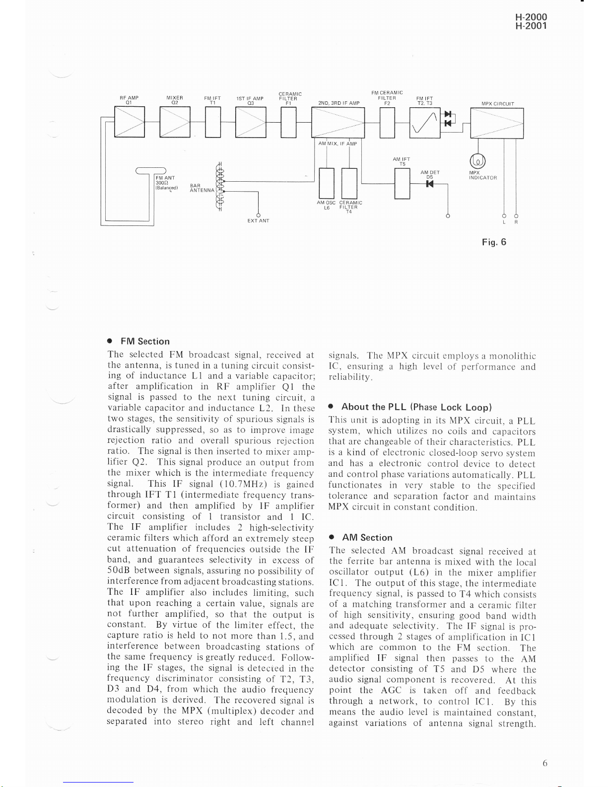
Section
The selected
FM
broadcast signal,
received
at
the
antenna,
is tuned
in
a
tuning
circuit
consist-
ing
of inductance
L I and
a
variable
capacitor;
after
amplification in
RF amplifier
Q
I the
signal
is
passed
to the next
tuning
circuit, a
variable
capacitor
and inductance
L2.
In
these
two stages,
the sensitivity
of
spurious
signals is
drastically
suppressed,
so as to improve
image
rejection
ratio and
overall spurious
rejection
ratio.
The signal is then
inserted to
mixer amp-
lifier
Q2.
This signal
produce
an output
from
the
mixer
which is the
intermediate
frequency
signal.
This IF
signal
(10.7MH2)
is
gained
through
IFT
T1
(intermediate
frequency
trans-
former)
and then
amplified
by IF amplifier
circuit
consisting
of
I transistor
and 1 IC.
The
IF
amplifier includes
2
high-selectivity
ceramic
filters
which
afford
an extremely
steep
cut attenuation
of frequencies
outside
the IF
band,
and
guarantees
selectivity
in excess
of
50dB
between
signals,
assuring
no
possibility
of
interference
from
adjacent
broadcasting
stations.
The IF
amplifier
also includes
limiting,
such
that
upon
reaching
a
certain
value,
signals are
not further
amplified,
so that
the
output
is
constant.
By virtue
of
the limiter
effect,
the
capture
ratio
is held
to
not
more
than
1.5,
and
interference
between
broadcasting
stations
of
the
same frequency
is
greatly
reduced.
Follow-
ing
the
IF stages,
the
signal
is
detected
in the
frequency
discriminator
consisting
of
T2,
T3,
D3
and
D4,
from
which
the
audio frequency
modulation
is
derived.
The
recovered
signal is
decoded
by
the MPX
(multiplex)
decoder
and
separated
into
stereo
right
and left
channel
AN/I IFT
T5
I\4PX
INDICATOR
cE R At\4 tC
FILTER
r4
Fis.
6
signals.
The
MPX circuit
employs
a monolithic
IC, ensuring
a
high
level
of
performance
and
reliability.
o
About
the PLL
(Phase
Lock
Loop)
This unit
is
adopting in
its
MPX
circuit,
a PLL
system,
which utilizes
no
coils
and
capacitors
that
are changeable
of
their characteristics.
PLL
is
a kind
of electronic
closed-loop
servo
system
and
has
a
electronic
control
device
to
detect
and
control
phase
variations
automatically.
PLL
functionates
in very
stable
to the
specified
tolerance
and separation
factor
and
maintains
MPX
circuit
in constant
condition.
o
AM Section
The selected
AM broadcast
signal
received
at
the ferrite
bar
antenna
is
mixed
with the
local
oscillator
output
(L6)
in
the
mixer
amplifier
IC
1.
The output
of
this
stage, the
intermediate
frequency
signal, is
passed
to
T4 which
consists
of a
matching transformer
and
a ceramic
filter
of
high
sensitivity, ensuring
good
band
width
and
adequate selectivity.
The IF
signal
is
pro-
cessed
through
2 stages
of
amplification
in IC
I
which
are
common to
the
FM
section.
The
amplified
IF signal
then
passes
to
the
AM
detector
consisting of
T5 and
D5
where the
audio
signal
component
is
recovered.
At this
point
the
AGC
is taken
off
and
feedback
through
a
network,
to
control
IC
1.
By this
means
the
audio
level
is
maintained
constant,
against
variations of
antenna
signal
strength.
RF
AMP
o1
IV]IX E R
a2
FM IFT
T1
MPX
CIRCUIT
AI\,1 DET
D5
FIVI CERAIVIIC
FILTER
2ND,3RD IF AMP
F2
o'r'''
u
AMOSC
Page 8
CABINET ASSEMBTY
(cMX-085-0)
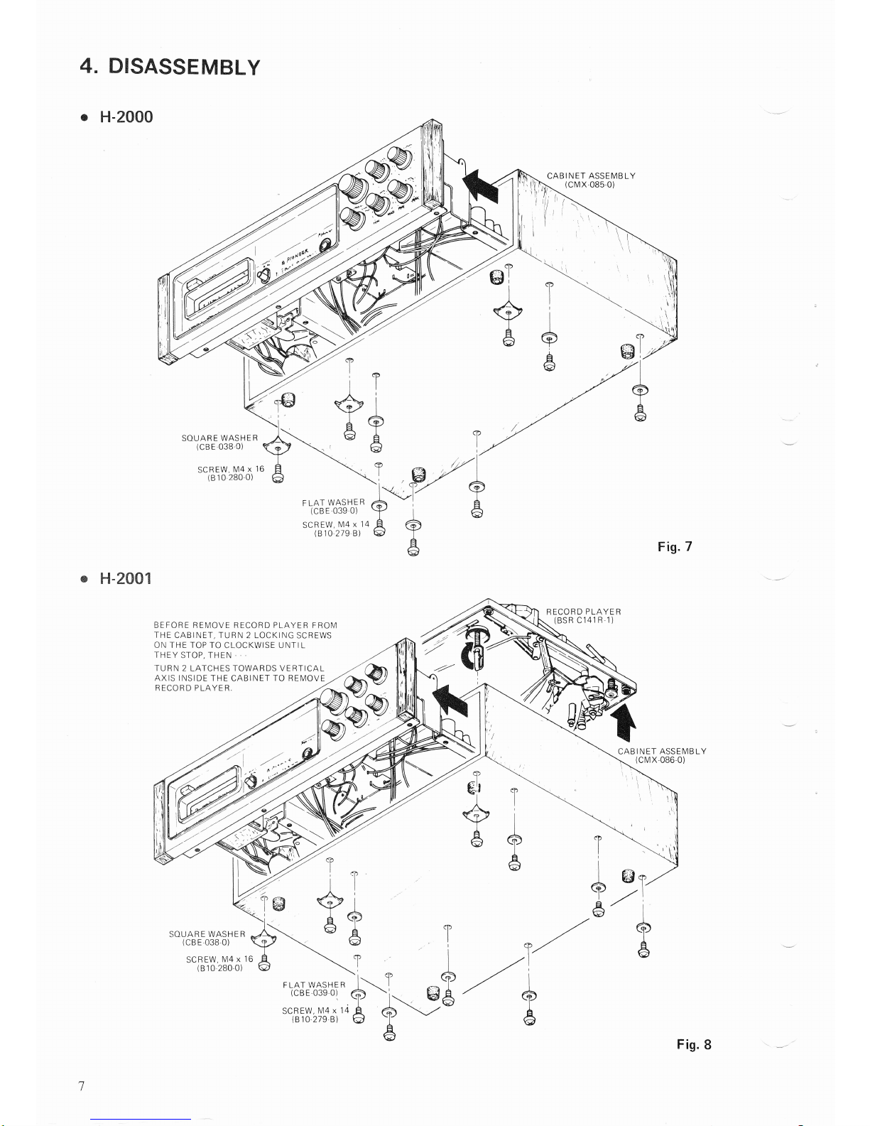
4. DISASSEMBLY
o
H-2000
@
ht-2001
7
Fis.
7
CABINET
ASSEMBLY
(cMX-086-0)
2L
A
T
I
e
6
'r
A
A
-?
glt
I
+
A
'f
'/
A .'\/
E'/
+
6
SOUARE
WASHER
(cBE
038
0)
SCREW,
M4
x
16
(810
280
0)
BEFORE
REMOVE RECORD
PLAYER
FROM
THE
CABINET, TURN 2 LOCKING
SCREWS
ON THE TOP TO
CLOCKWISE UNTIL
THEY
STOP, THEN
TURN 2
LATCHES
TOWARDS VERTICAL
AXIS INSIDE
THE CABINET
TO
REMOVE
RECORD PLAYER.
SOUARE
WASHER
(cBE
038 0)
SCREW,
M4
x
16
(810
280
0)
FLAT WASHER
(cBE
039
0)
SCREW,
M4
x 1'
(810
279-B)
RECORD
PLAYER
(BSR
C141R
1)
Fis.
8
Page 9
H-2000
H-2001
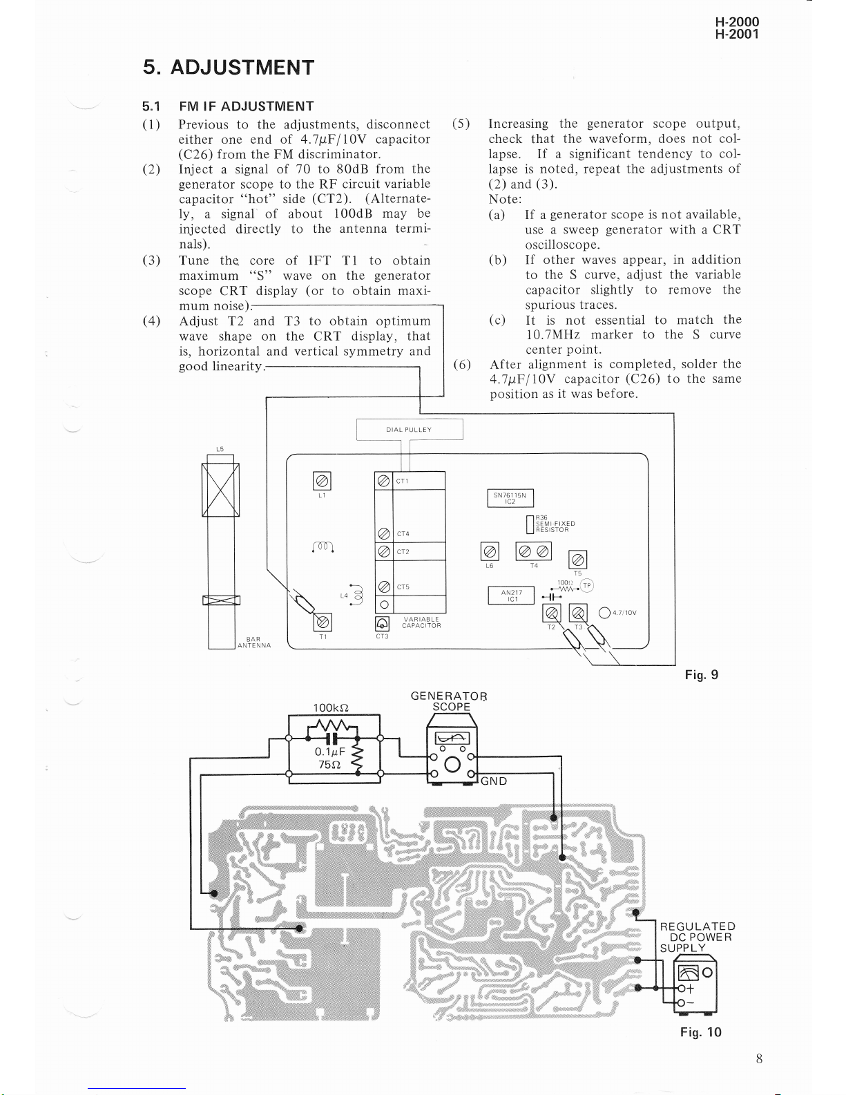
5.
ADJUSTMENT
5.1
FM
IF ADJUSTMENT
(
1)
Previous
to the adjustments,
disconnect
either one end
of 4.7
ltF
I
I 0V capacitor
(C26)
from
the FM
discriminator.
(2)
Inject a signal of 70
to
B0dB
from
the
generator
scopg to
the RF
circuit
variable
capacitor
"hot"
side
(CfZ). (Alternate-
ly,
a
signal
of
about
100d8 may
be
inj
ected
directly
to
the antenna
termi-
nals)
(3)
Tune the core of IFT T 1
to
obtain
maximum
6(5"
wave
on the
generator
scope
CRT
display
(or
to obtain
rnaxi-
mum noise)
(4)
Adjust T2
wave shape
is, horizonta
good
linearit
Increasing
the
generator
scope
output"
check that
the
waveforil, does
not col-
lapse. If a
significant tendency to
col-
lapse is
noted, repeat
the
adjustments of
(2)
and
(3).
Note:
(a)
If a
generator
scope
is not
available,
use
a sweep
generator
with
a
CRT
oscilloscop
e.
(s)
(b)
If
other waves appear,
to
the S
curve, adjust
capacitor
slightly to
spurious
traces.
in
addition
the
variable
remove the
match
the
he
S
curve
1, solder
the
to the same
Fig.9
REGU
LATE
D
DC
POWE R
SUPPLY
BA
ANTE
GENERATOB
SCOPE
1 00ka
.;iiiiiiiiiirrii'lil:;-;rliili
#.iiiiiriitiiliiiii.ii;il
ffi#u'#
GND
L5
X
.--
and
T3
to obtain optimum
on the
CRT
display, that
rl and vertical
symmetry and
v.
DIAL PULLEY
-l
(
c)
It is
not
essential to
l}.7MHz
marker to
tl
center
p
oint.
(6)
After
alignment
is
completed
a.1
ptr
l10V
capacitor
(C26)
t
position
as
it
was before.
l-Jrr:i1ls- I
Irczl
r-1R36
I lsrvt-FlxED
!
nesrsron
WW@
r 00,,T5,4:r
l_^*n
{ff.y
@@
oazrrov
@l
@t,
ll
r.q
\.
N"3
\R
I
r1
ENNA \
@
C
a
CT2
@
CT5
o
@
--ffi
ffi
Fis"
10
Page 10
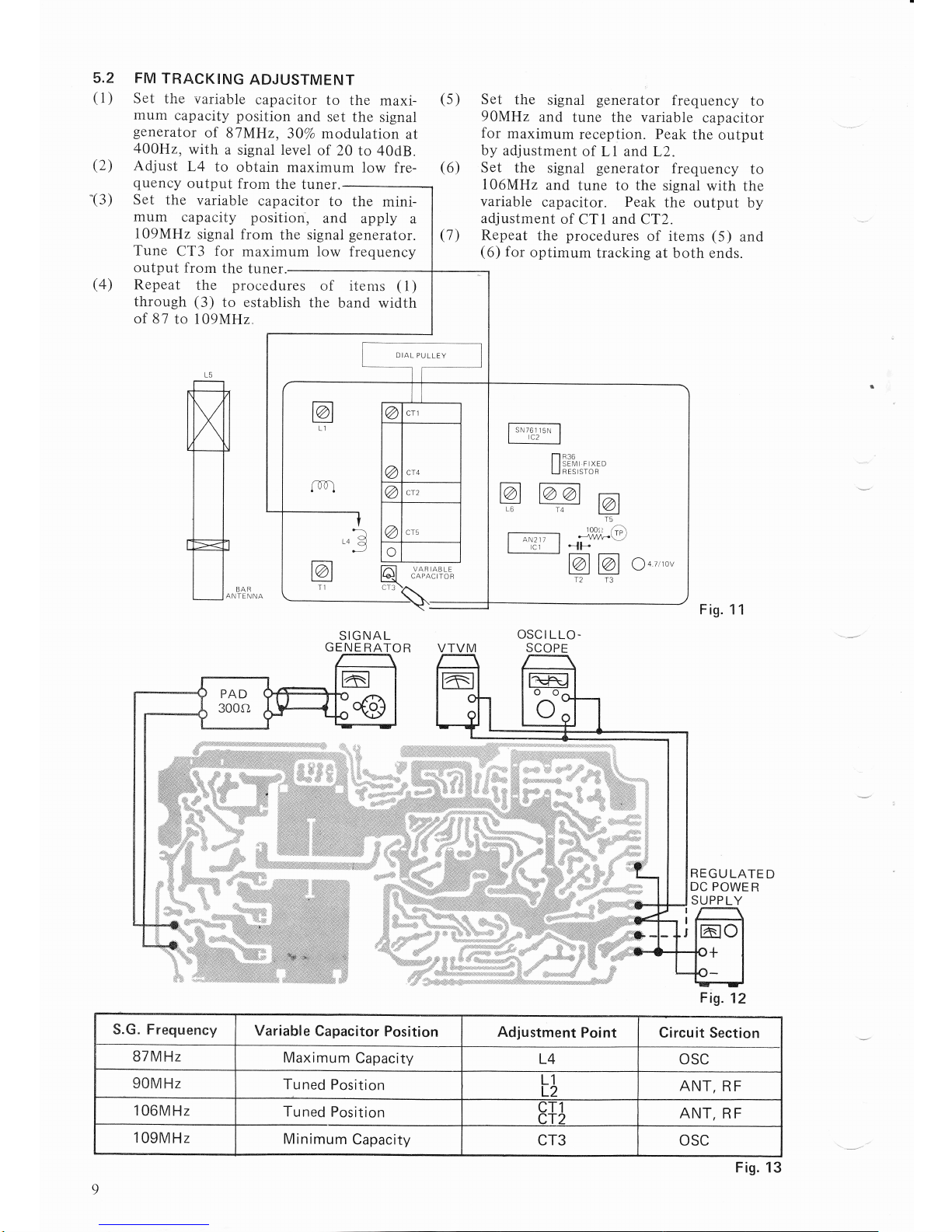
5.2 FM
TRACKING
ADJUSTMENT
(
I
)
S
et
the
variable
capacitor
to
the
maxi-
mum
capacity position
and
set the
signal
generator
of
87MHz,
30% modulation
at
400H2,
with
a
signal level
of
20 to
40dB.
{2)
Adjust
L4
to
obtain
maximum
low
fre-
quency
output
from
the
tuner.
Set
the
variable
capacitor
to
Set
the
signal
generator
frequency
to
90MHz
and
tune the variable
capacitor
for
maximum
reception.
Peak
the output
by
adjustrnent
of
L1
andL2.
S
et
the
signal
generator
frequency
to
tr 05MHz
and
tune to the
signal
with
the
variable
capacitor. Peak
the output
by
adjustment
of
CT1
and
CT2.
Repeat
the
procedures
of items
(
5
)
and
(6)
for
optimum
tracking at both ends.
'(3)
(s)
(6)
(t)
(4)
mum
capacity position,
and
109MHz
signal
from
the signal
Tune
CT3 for
maximum low
output
from
the
tuner.
Repeat
the
pro0edures
through
(3)
to
establish
of 8l
to 109MHz.
the
mini-
apply
a
generator.
frequency
of
items
(
1)
the
band
width
@
@]
.ufoX8,'rb'*
"'\,_
SIGNAL
GENE
RATOR
VTVM
OSCI
LLO-
SCOPE
F
ig. 11
REGULATED
DC
POWE
R
SUPP
LY
L5
X
:
DIAL
PULLEY
I
sN?61rsr_l
I
rcz
I
lii!,rm"
@@@
L6
T4
T5
1nn() /.\
m---{ilo*v
@@
oo,,,ou
Fig.
12
S.G. Frequency
Variabl
e Capacitor
Position
Adjustment
Point
Circuit
Section
87lVl H
z
Maximum
Capacity
L4
OSC
90M l-lz
Tu
ned
Position
L1
L2
ANT,
R F
1 06M Hz
Tu
ned Position
CT1
CT2
ANT,
R
F
1
09MHz
M
in imu
m
Capacity
CT3
OSC
Fig. 13
Page 11
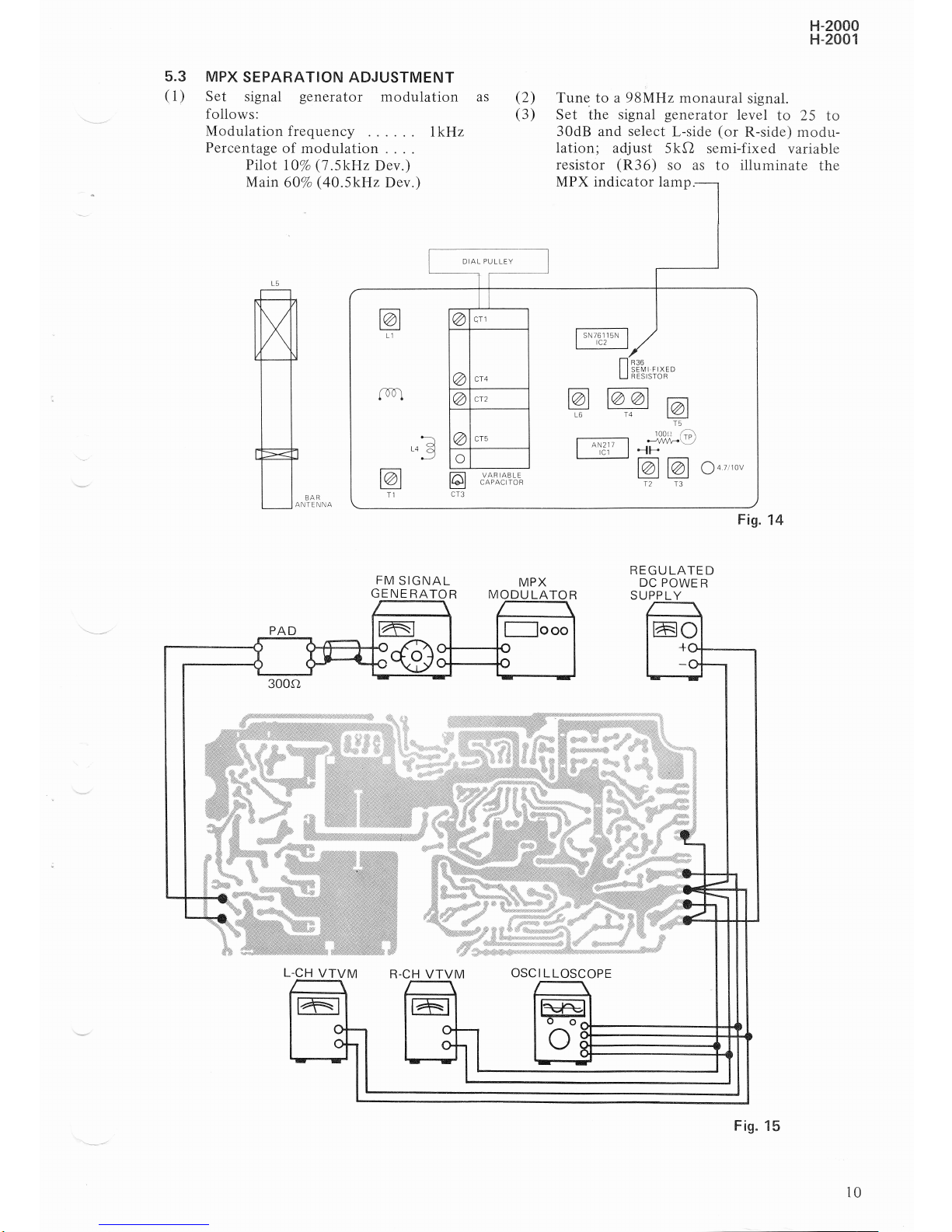
5.3
MPX
SEPARATION ADJUSTMENT
(
1)
Set signal
generator
modulation
follows:
IVlodulation
frequency
IkHz
Percentage
of
modulation
Pilot
l0%
(1
.skHz
Dev.)
Main
60%
(40.5kH2
Dev.)
H-2000
!-t-200
t
(2)
Tune to a
gBMHz
monaural
signal.
(3)
Set the
signal
generator
level
to
25
to
30dB and
select
L-side
(or
R-side) modu-
lation;
adjust
5kQ
semi-fixed
variable
resistor
(R3
6)
so as
to illuminate
the
MPX indicator lamp,
AS
L5
X
DIAL
PULLEY
R36
SEM
I,F
IX ED
RESISTOR
1#
BAR
ANTE NNA
FM
SIGNAL
GENERATOR
PAD
300Cl
L-CH
VTVM
R-CH VTVM
MPX
MODU
LATO
R
OSC I
L
LOSCOPE
REGULATED
DC
POWE
R
SUPPLY
Fis"
14
Fig.'15
10
Page 12
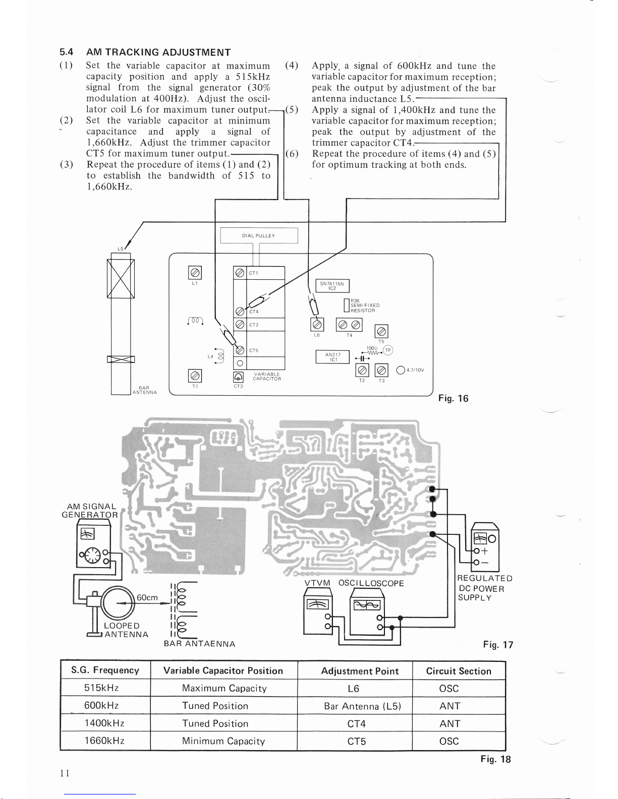
5.4
(1)
!r)
(3)
AM
TRACKING
ADJUSTMENT
Set the
variable
capacitor
at
maximum
capacity
position
and apply a
5
l5kHz
signal
from
the signal
generator
(30%
modulation
at 400H2).
Adjust
the oscil-
lator
coil
L6
for
maximum tuner output,
Set the variable
capacitor at minimum
capacitance
and
apply a
signal
of
1,660kH2.
Adjust
the
trimmer
capacitor
CT5
for
maximum
tuner output.
Apply.
a signal
of
600kHz
and
tune
the
variable
capacitor
for maximum
reception;
peak
the
output
by
adjustment
of
the bar
antenna
inductance
L5.
Apply
a signal
of 1,400kH2 and
tune
the
variable
capacitor
for maximum
reception;
peak
the output
by
adjustment
of
the
trimmer
capacitor
CT4,
(4)
(s)
(6)
Repeat the
procedure
of items
(
1)
to
establish
the
bandwidth
of
I,660kHz"
Repeat
the
procedure
of
for
optimum
tracking
at
items
(a)
and
(5)
both ends.and
(2)
515 to
BAR
NTEN
NA
iF-
BAR ANTAENNA
;
e_
X
-
DIAL PULLEY
lvl I
@@
o+zrrov
@
."f i8,?b?
12
13
Fis.
16
LOOPE
D
ANTE
NNA
**$
ry
;*ln+n-#
I I
*i***ffi
Eo
o+
o-
ffi
L
liiiiiliiiiiiiiiiil'i.i
VTVM
iiiiiilill,iiiiiii:ljriii'ii;iil
CSC
I
L
LOS(
REGULAI
DC
POWE
Supp
r_y
tFl
o
o
ffil
1
.ED
R
F
ig.
',7
S.G. Frequency
Variabl e Capacitor
Position
Adiu
strnent Point Circuit Section
51skHz
Maximum
Capacity
L6 OSC
600k H
z
Tu
ned Position
Bar Antenna
(L5)
ANT
1 400kHz
Tu ned
Position
CT4
ANT
1660kHz
Minimum
Capacity
CT5
OSC
F ig.
18
11
Page 13
H-2000
H-2001
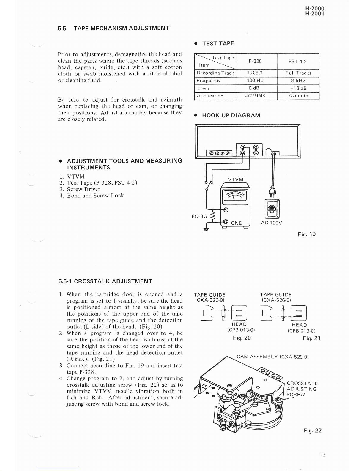
5.5
TAPE MECHANISM
ADJUSTMENT
Prior
to adjustments,
demagnetize
the
head and
clean
the
parts
where
the
tape threads
(such
as
head,
capstan,
guide,
etc.)
with
a soft
cotton
cloth
or swab moistened
with
a
little
alcohol
or cleaning fluid
Be sure to adjust
for
crosstalk and azimuth
when replacing the
head
or
cam, or
changing-
their
positions.
Adjust
alternately because
they
are
closely related.
O
ADJUSTMENT
TOOLS
AND
MEASURING
INSTRUMENTS
1. VTVM
2.
Test
Tape
(P-328,
PST
-4.2)
3. Screw
Driver
4.
Bond
and
Screw
Lock
5.5.1
CROSSTALK
ADJUSTMENT
1.
When the
cartridge door is opened
and
a
program
is
set
to I
visually,
be
sure the head
is
positioned
almost at the same height as
the
positions
of the
upper
end
of
the
tape
running of the tape
guide
and
the
detection
outlet
(L
side)
of
the
head.
(Fig.20)
2.
When
a
program
is
changed
over
to 4, be
sure
the
position
of the
head is almost at the
same height as
those of the
lower
end
of
the
tape running and
the
head detection
outlet
(R
side).
(Fie
.
2I)
3.
Connect
according to
Fig.
19 and insert test
tape
Pr328.
4.
Change
program
to 2,
and adjust by
turning
crosstalk adjusting
screw
(Fig
.
22) so as
to
minimize
VTVM
needle
vibration
both
in
Lch and Rch. After adjustment, sec-ure ad-
justing
screw
with
bond and
screw lock.
O
TEST
TAPE
O
HOOK
UP
DIAGRAM
TAPE
GU
IDE
(cx
A-526-0)
F
is.
19
TAPE
GUIDE
(cxA-5
26-0l
---
-Tast
Tape
Item
\\
P
-328
PST-4.2
Recording
Track
1
,3,5,7
F
u ll Tracks
Frequency
4OO Hz
B kHz
Lever
o dB
13
dB
Application
Crosstalk
Azimuth
E$tr
E+E
HEAD
(cPB-013-0)
F is.
20
CAM ASSE
M B LY
(CXA-529-O)
HEAD
(cPB-013-0)
Fig.
21
CROSSTALK
ADJUSTING
SC
REW
Fig.22
l2
Page 14

1.
5
"5.2
AZIMUTH
ADJUSTME
NT
Connect
according
to Fig. 19
and
insert
test
tape PST-4.2.
Change
program
to
3
and adjust
by turning
azimuth
adjusting
screw
(Fie.
23) to secure
maximum
output reading
on the VTVM in
both
Lch
and
Rch.
5.5.3
ADJUSTMENT
OF
MOTOR
PULLEY
POSITION
1. When
replacing
motor
pulley
or
motor,
in-
stall
as
shown in
Fig. 24,
adjust
position
adjusting
screws
and
leave
a space
of
approx.
6.Omm
(Il4
in.)
between
pulley
and motor
CASE.
5.5-4
AD.JUSTMENT
OF
CARTR
IDG
E LOCK
PR
ESSU
R E
1.
Measure
the
end
of
the
pressure
roller
with
a
tension
gauge.
(F
ie. 25)
2.
Adjust
the installment position
of
the
pres-
sure sp
ring
so the
p
ointer
of
the
tension
gauge
will
indicate
approx
.
1.4 kg
(3.1
lbs).
6.
DIAL
STRINGING
CAM' ASSE
M
B LY
(CXA-529-O)
MOTOR PU
LLEY
(cxA-530-0)
114
in.l
2.
AZIMUTH
ADJUSTING
SCREW
POS
ITION
ADJUSTI
NG
SC R EWS
F ig.
23
Fig,24
F ig.
25
PRESSURE
ROLLER
ASSEMBLY
INSTALLMENT POSITIONS
cou
nterclockwise
MOTOR
(cxM-019-0)
(cxA-532-0)
PRESSURE
SPRING
cB
H
-124-Ol
1.4
kg
(3.1
lbs)
13
Fig.26-'-.--
Page 15

Page 16

Page 17

Page 18

Page 19

H-2000
H-2001
Ref.
Key Parts
No.
Description
N otes
c51
c53
c54
c55
u5t
L5/
c58
c59
c60
c61
c62
c63
U fr4
c65
c03-21
9-M
c03-219-M
c03-219-M
c03-219-M
c03-230,M
c03-230-M
c00-550-P
c03-241-M
col-153
Z
C10-050-J or
c05,041-J
c03,259-M
co3-263 M
co3-241-M
CCF-002-O
or
cc
L-020-o
c00-547 P
Capacitor,
COlvlA502l\1
50
Capacitor, COMA502N/
50
Capacitor,
COMA502IVI 50
Capacitor,
COMA502M50
Capacitor.
COIVIA'1 03M50
Capacitor,
COMA103
M50
Capacitor.
CEA331P1
6
Capacitor.
COMA403M50
Capacitor, C K DY F 203250
Capacitor, CMA471J50
Capacitor, COSA471J50
Capacitor,
CON/
A2241\,{
50
Capacitor, CON/ A334M
50
Capacitor,
COlvlA403M50
Capacitor, CMA 1 72J50
Capacitor.
COSA172J50
Capacitor,
CEA221P16
50v
50v
50v
50v
50v
50v
16V
50v
50v
50v
47OpF t5%
O.22pF t2O%
0.33p F x2oo/o
0 04pF
r2O%
1
700pF x5%
0.005pF
0.005pF
0.005pF
0.005pF
0.01pF
0.01pF
330pF
O.O4pF
O.O2pF
47OpF
t20%
x20%
t2O%
t200/.
t20%
t2Oo/o
t20%
l8O
o/
20
/o
t5%
50v
50v
50v
50v
50v
1
70OpF
22OttF
t5o/o
50v
i6v
MISCELLANEOUS
Ref.
Key
Parts
No.
Description
N
otes
o1
02
o3
D1
D2
D3
D4
D5
tc.1
1C2
L1
L2
ta
L4
L6
L7
LO
T1
T2
T3
I4
Ttr
VC
CT-3
F1
F2
G08-006-c
G05 004-B
G05-062-B,C
G00-010-A
G 00-0 1
0-A
G00-004-A
G00,004-A
G00-010-A
G09-024,E,F
G09-023-A
cTC-020,0
cTC-021-O
cTC,023-O
cTC.O22-O
cTE-027-O
cTE-030,o
cTE-030-O
cTC-024-O
cTC-025-O
cTc-026-o
cTE-028-O
cTE-029-O
cc K-006-0
cc L-01
9-o
cTF-032-O
cTF-032-O
FET,
25K41 E
Transistor,
25C461
B
Transistor,
2SC380
O,
Diode, 1S
188
A{Vl
Diode,
1S188 AM
Diode, 1S
188 FM
Diode,
1S188
FM
Diode,
1S
188
AM
IC,
AN217
BB,CB
IC,
SN 161 15N
FM
ANT
Coil
FM
RF
Coil
Trapping
Coil
FM
OSC
Coil
AM OSC
Coil
Co il
Coil
Flvi
1st
lF Transf
ormer
FM
2nd lF
Transformer,
Primary
FM
2nd lF
Transformer,
Secondary
AM
1st lF
Transf
ormer
AM
2nd
ll: Transtormer
Variable
Capacitor
Trimmer
Capacitor
Ceramic
F ilter
Ceramic Filter
22
Page 20

v
"4
ESUAT_!ZER
UN
!T
(CWK-079-0)
&
Parts
Con
nectlon
TO
L-CH
HEAD
:r
"}'o
HEAD
SH
IE
LD
WIRES
TO R-CH
HEAD
TO
POWE
R
SU
PP
LY
THRU VOLUME
CONTROL
UN
lT
+B
TO
R-CH ROTARY
SW
(S2)
F
is.
30
23
Page 21

t-t-2000
H-2001
o
Parts
List
RESISTORS
Parts
No.
Description
Notes
R
101
R103
R104
R105
R106
R107
R108
R 109
R1'1 0
R111
R112
R113
R114
R115
R1 16
R117
R118
R',] 19
R120
R121
R122
R123
Rl24
Y05-28 7,J
Y05-349-J
Y05-293-J
Y05-310-J
Y05-346-J
Y05-258-J
Y05-284-J
Y05-321-J
Y05-368-J
Y05-333-J
Y05,310-J
Y05-281-J
Y05-349-J
Y05-293-J
Y05-310-J
Y05-346-J
Y05-258-J
Y05-284-J
Y05-321-J
Y05-368-J
Y05-333-J
Y05-310-J
YO5-287-J
Resistor. RD1/4VS102J
Resistor. RD1i4VS154J
Resistor,
RD1
l4VS222J
Resistor, RD1/4VS682J
Resistor, RD1/4VS104J
Resistor, RDl/4VS101J
Resistor, RD1/4VS821J
Resistor, RD1/4VS183J
Resistor, RD1/4VS684J
Resistor, RD1/4VS473J
Resistor,
RD1/4VS682J
Resistor,
RD1/4VS102.j
Resistor, RD1/4VS154J
Resistor.
RD1
l4VS222J
Resistor. RDl/4VS682J
Resistor.
RD1/4VS104J
Resistor.
RD1/4VS101J
Resistor, RD1/4VS821J
Resistor,
RD1/4VS183J
Resisror, RD1/4VS6B4J
Resistor, RDl/4VS473J
Resistor. RD1/4VS682J
Resistor,
RD1/4VS102J
1kst
1
50ka
2.2kA
6.8
ks)
1
00ko
1 00a
820f,)
18kf,2
680kf)
41kA
6.8ksl
1kA
1
50ka
2.2ka
6.BkA
1
00k{',
1
00a
820a
1
8kO
680ko
41ka
6.8
ka
1ka
t5o/o
t5o/o
t5o/o
t5%
t5%
t5%
r5%
t5%
t5%
t57.
t5%
t5%
t5o/o
r5o/o
t5%
!5%
t5%
t5%
!5%
t5%
t5%
t5%
t5o/o
1
t4W
1
l4W
1
l4W
1
l4VU
1
l4W
1
l4W
1
l4W
1
l4W
1
l4W
1
l4W
1l4V,l
1
l4W
1
l4W
ll4VU
1
l4\N
1l4W
1
l4W
1
l4W
1
l4Vl
1
l4\^t
1
l4W
1
l4W
114\N
CAPACITORS
Parts No-
Description
N otes
c1 01
c102
c103
c104
c1
05
c1 06
c1 07
c108
c109
c110
c1 15
c1 16
c1
11
c118
c1 19
c0B-060-K
c00,213-P
c00-533-P
c08-040-K
c00-213-P
c00-230-P
c03-219-N/
c08-060-K
c00-21
3
P
c00-533-P
c08-040-K
c00-213-P
c00-230-P
c03-219-M
c00-547-P
Capacitor,
CCDSL681 K50
Capacitor,
CEA4R7P10
Capacitor,
CEA470P16
Capacitor,
CCDSLl 01 K50
Capacitor,
CE,A4R
7P 10
Capacitor,
CEA330P10
Capacitor,
COMA50ZM50
Capacitor,
CCDSL63i K50
Capacitor,
CE44R7P10
Capacitor,
CE4470P
16
Capacitor.
CCDSLl
01 K50
Capacitor,
CE44R 7P 1O
Capacitor,
CEA330P10
Capacitor,
COMA50ZM50
Capacitor,
CEA221P16
680pF t1O%
4.7
pF l'?3%
47pF
I'l3z
100pF
xloo/o
4.71tF
l'u,o,%
aa,,E
+100n,
0.005pF r2oo/"
680pF
!1oo/o
4.71tF I'i8%
47pF I'13%
100pF
xlO%
4.71tF
:'i3%
33pF
I'13%
0.005pF t2Oo/"
22opF I'13%
50v
10v
16V
50v
10v
10v
50v
50v
10v
16V
50v
10v
10v
50v
16V
MISCELLANEOUS
Ref. Key Parts No.
Description
N otes
01 01
01 02
o103
o104
G05-0
G05-4
G0s-0
G05-4
2-FG
1-C,D
2-F,G
1-C.D
Transistor,
2SC732 BL.G R
Transistor,
2SC733 Bl-,GR
Transistor,
2SC732 BL,G R
Transistor,
2SC733 BL,GR
24
Page 22

7,5
VOLUME
CONTROL
UNIT
(CWK.O8O.O)
Parts
Connection
TO R-CH
PHONO
ROTARY
SW
(S2)
PHONO
INPUT
JACI<(J2-1),
H-2OOO;
PHONO
INPUT
PLUG
(P2).
H
2OO1
TO
ROTARY
SW
(S2)
GROUND
TO
R-CH
TO
R-CH
TO
R-CH
ROTARY
SW
(S2)
MAIN
TERMINAL
TO
L-CH
ROTARY
SW
(S2)
MAIN
TE
RM
INAL
tO
TUNER
UNITcROUND
rTO
TONE
CONTROL
UNIT
GROUND
TO
L-CH
TONE
CONTROL
INPUT
TO L-CH
LINE
CUT JACK
(J2-1)
,
H-2001
ONLY
TO LINE
OUT
GROUND
TO
R-CH
LiNE
OUT
JACK
(J2-11
,
H.2OO1
ONLY
VOLUME
CONTROL
UN IT
+B
TO
L-CH
PHONO
INPUT
JACKQ2-1
),
H-2000;
TO
L-CH
PHONO
tNpUT
pLUG
(p1).
H
-2001
TO
L
CH
PHONO
ROTARY
SW
(S2)
TO PHONO
INPUT
JACK
(H-2OOO)
OR
PLUG
(H-2001)
GROUND
F
ig.
3'l
TO
R-CH
TONE
CONTROL
INPUT
25
Page 23

H-2000
H'zO/.r1
o
Parts
List
RESISTORS
Ref.
Key Parts
No.
Description
Notes
R 201
R202
R203
R204
R205
R
206
R20l
R208
R209
R21 0
R21
1
R212
R21
4
R21 5
R21
6
R211
R21
B
R21 9
R220
R221
R222
Y05-37s-J
Y05-357-J
Y05-385-J
Y05-314-J
Y05,214-J
Y05-298-J
Y05-385 J
Y05-298-J
Y05-284,J
Y05-258-J
Y05-375-J
Y05-35
7,J
Y0s-385-J
Y05-314,J
Y05-214-J
Y05-298-J
Y05
385
J
Y05-298
J
Y05-284-J
Y05-287 J
Y05,328-J
YO5-328-J
Resistor, RD1/4VS'105J
Resistor,
RDl/4VS334J
Resistor,
RD1/4VS335J
Resistor. R D1l4VS822J
Resistor, RD1/4VS471J
Resistor, RD'1/4VS332J
Resistor, RD1/4VS335J
Resistor, RD1/4VS332J
Resistor, RD1/4VS821J
Resistor,
RD1/4VS101J
Resistor. RD1/4VS105J
Resistor, R D 1/4VS334J
Resistor,
R D 1/4VS335J
RESiStOr, R D1/4VSB22J
Resistor,
RD1/4VS471J
Resistor, RD1/4VS332J
Resistor, RD1/4VS335J
Resistor, RD1/4VS332J
Resistor. R
D 1/4VS821J
Resistor, RD1/4VS102J
Resistor,
RD1/4VS333J
Resistor. R
D
1/4VS333J
1MA
330ko
3.3Mf,,
8.2ko
410{t
3.3kO
3.3Ms)
2 2t,o
820s,
1
00s}
1Mf)
330ka
3.3MA
8.2ka
4loa
3.3ka
3
3Ml]
3.3ks)
8
20S)
1 ks?
33kJ-)
33kJ
)
t5%
t5%
t5%
t5%
r5./o
i:54/o
t5o/o
t5%
\5%
t5%
x5%
t5%
t5%
t5%
t5%
x5%
r5%
!5%
t5%
r5%
!5%
L5%
1
l4\tN
1
l4W
1
l4W
1
l4Vl
1
l4W
1
l4\N
1
l4\N
1
l4W
1
l4W
1
l4W
1
l4VU
1
I
4v\l
1
l4\^t
1
l4Vr
1
l4W
1
l4W
1
l4V'l
1
l4\,N
1
l4W
1
l4\N
1
l4VU
1
l4\N
CAPACITORS
Re{. Key Parts
N o.
Description
N otes
c201
c202
c203
c204
c205
c206
c201
c208
c209
c210
c02,401 Nt
coo-222-P
c02 401-M
coo-222
P
c00-550-P
c00-550-P
c02,401 M
coo-222
P
c02-401
-M
coo 222-P
Capacitor, CSYA0R 1M25
Capacitor,
CEA'i00P
10
Capacitor,
CSYA0R
1M25
Capacitor, CEA100P10
Capacitor.
CEA331P16
Capacitor, CEA331P16
Capacitor,
CSYA0R
1M25
Capacitor, CEA1OOP10
Capacitor, CSYA0R 1M25
Capacitor.
CEA100P'1 0
0.1
pF
1
0pF
0.1pF
'1
0pF
330pF
330pF
0.1
pF
1
0pF
0.1pF
1
0pF
20v" 25V
'i3%
1ov
20%
25V
'ii%
'1
ov
'ilz
16v
'i'32
16v
20%
25V
'13%
1ov
20%
25V
'i3%
rov
MISCE
LLANEOUS
Ref. Key
Parts
No.
Descr
ipt io n
Notes
o201
o202
o203
o204
VR1
VR2
G05,012-F,G
G05-012-G
or
G06-003-G
G05-012-F,G
GO5-012-G
or
G06 003 G
ccv-006 0
ccv,007,0
Transistor,
25C733
BL,GR
Transisror.2SC733 BL
Transistor,
25C9O0 U
Transistor,
2SC733 BL,G R
Transistor,2SCT33 BL
Transistor. 2SC9C,0 U
Variable Resistor, 10kfz(A)
Variable
Resistor. 50kJ){BH
)
Volume
Control
Balance
Coutrol
26
Page 24

7.6 TONE
CONTROL
UNIT
o
Parts
Connection
(cwK-081-0)
TO
R-CH
VOLUME
CONTROL
UN
IT
OUTPUT
TO VOLUME
CONTR
O
L
UNIT
GROUND
TO
L-CH
VO LUME
CONTR
O L
UN IT
OUTPUT
TO R-CH
AMPLIFIER
U N
IT INPUT
TO AMPLIFIER
UNIT
GROUND
TO
L-CH
AMPLIFIER
UN IT
INPUT
F
ig. 32
27
Page 25

H-2000
H-2001
o
Parts
List
RESISTORS
Ref.
Key Parts No.
Description
Notes
R 301
R302
R303
R
304
R305
R306
R 307
R
308
R309
R31
0
Y05-317,J
Y
05-27 4-J
YO5-293-J
Y05-307-J
Y05-298-J
Y05-3'1
7-J
Y05-274-J
Y05-293-J
Y05
307-J
Y05-298-J
Resistor,
RD1/4VS103J
Resistor,
RD1/4VS471J
Resistor,
RDIl4VS222J
Resistor.
R D1/4VS562J
Resistor,
RD1/4VS332J
Resistor,
RD1/4VS103J
Resistor,
RD1/4VS471J
Resistor,
RD1l4VS222J
Resisror. RD1/4VS562J
Resistor.
RD1/4VS332J
10kA
x5%
1l4W
41OA x5%
1l4W
2.2kA t5%
1l4W
5.6k'a x5%
1l4W
3.3k4 r5o/o
1l4W
10ka
t5%
1l4W
4loa
t5%
1l4W
2.2k{L !5%
1l4W
5.6k4 r5o/o
1l4W
3.3k'a !5%
1l4W
CAPACITORS
Ref.
Key
Parts No.
Description
Notes
c301
c302
c303
c304
c305
c306
c307
c308
c03-208-M
c03-234-M
c03,234-rvl
c03-254-M
c03,208,M
c03-234,N/
c03-234-M
c03-254-M
Capacitor,
COlVlA202M50
Capacitor,
COMA203M50
Capacitor,
COMA203M50
Capacitor,
COMA 1 04N/50
Capacitor.
COMA2O2M50
Capacitor.
COMA203M50
Capacitor,
COMA203M50
Capacitor.
COMA 1 04N/50
O.OO21tF t2O%
50V
O.O21IF !2O%
50V
O.O21tF
t2O%
50V
0.1pF x2O%
50V
0.002pF t2O%
50V
O.O21:F
t2O%
50V
O.O21tl x2O%
sOV
0.1rrF x2O%
50V
MISCELLANEOUS
Re{ Key
Parts N o.
Description
Notes
VR3
VR4
ccv-008-0
ccv-008-0
Variable
Resistor.
50kf,2(A)
Variable
Resistor,
50ks}(A)
Treble
Control
Bass Control
28
Page 26

7.7 AMPLIFIER
UNIT
(CWK-082.N)
o
Parts
Connection
TO
L-CH
TONE
OUTPUT
o4CI3,
0407
2SC
1
173 C,R
,Y
x 2
TO HEADPHONE
JACK
NO.2TERMINAL
JUIVIPER
WIRE
GROUNDED
TO R-CH TONE
OUTPUT
0404, o40B
25A473
0,
R
,Y
x
2
TO
HEADPHONE
JACK
GROI.JND
TO
HEADPHONE
N0.6
TERMINAL
JAC
K
TO TONE
CONTROL
UN
IT
GROUND
29
AT
THE
CHASSIS
F is.
33
Page 27

H-2000
H-2001
.
Parts
List
RESISTORS
Ref. Key
Parts No. Description
Notes
R401
R402
R403
R404
R405
R406
R401
R408
R409
R41 0
R41 1
R412
R41 3
R41 4
R41
5
R41
6
R41 7
R41
8
R41
9
R420
R421
R422
R423
R424
R425
R426
R427
R42a
Y05-287-J
Y05-346-J
Y05,304-J
Y05-246,J
Y05-298-J
Y05-462,J
Y05-462-J
Y05-336-J
Y05-318-J
Y05-234-J
Y05-407-J
Y05-407-J
Y05-318-J
Y05 231,J
YO5-28 7-J
Y05-346-J
Y05-304-J
Y05
246,J
Y05-298-J
Y05-462-J
YO5 462,J
Y0s-336-J
Y05,318-J
Y05
234.J
Y05-407-J
Y05-407-J
Y05-23i-J
Y05-318-J
Resistor, RD1/4VS102J
Resistor,
RD1/4VS104J
Resistor,
RD1l4VS412J
Resistor,
RD1/4V547OJ
Resistor, RD1/4VS332J
Resistor,
RD1/2VS1B1J
Resistor, RD1/2VS181J
Resistor,
RD1/4VS563J
Resistor.
RD1/4VS123J
Resistor, RD1/4VS150J
Resistor. RD1/2VS0R5J
Resistor, RD1/2VS0R5J
Resistor, RD1/4VS123J
Resisror, R D1l4VS100J
Resistor, RD1/4VS102J
Resistor, RD1/4VS104J
Resistor, RD1
l4VS412J
Resistor, RD1/4VS470J
Resistor, RD1/4VS332J
Resistor.
RD1/2VS181J
Resistor,
RD1/2VS181J
Resistor. RD1/4VS563J
Resistor,
RD1/4VS123J
Resistor, RD1/4VS150J
Resistor,
RDl/2VS0R5J
Resistor,
RD1/2VSORbJ
Resistor,
RD1/4VS100J
Resistor. RD1/4VS123J
ika
1
00ko
4.7ks],
47A
3.3ks)
1
80S)
1 80f,
56kA
12k'].
1
5f,)
0 5s)
0.5A
1
2kf,2'
10a
1 ks/
1
00kA
4.7ko"
41{-L
3.3ka
1 80()
180a
56kA
1 2ksl
15A
05a
0.5a
i0f2
1 2k(2
t5%
t5%
t5%
t5%
r5%
r5%
r5%
x5o/o
t5%
!5%
t5%
!5%
t5%
x5%
t5%
t5o/o
t5%
t5%
!5%
\5%
\5%
x5%
r5%
t
5a/o
t5%
t5Y.
t5%
t5%
1
l4W
1
l4V\
1
l4W
1
l4W
1
l4W
1l2W
1l2W
1
l4W
114\N
1l4W
1l2W
1l2W
1
l4W
1
l4W
ll4Vr
1
l4W
1l4W
1l4V\
1l4W
1l2W
1l2W
1l4V\
1
l4W
1
l4W
1l2W
1l2W
1
l4W
1l4W
CAPACITORS
Flef, Key Parts No.
Description
N otes
c40'1
c402
c403
c404
c405
c406
c407
c408
c409
c41
0
c41 1
c412
c413
c41 4
c41 5
c4'1
6
c41l
C41 B
c419
c420
c03-204-M
c00-730-P
coo-222-P
c00-547-P
c08-048-K
c00-530-P
c00-553-P
c06-161-K
c02-401-M
c03-204-M
c00-730-P
coo-222-P
c00 547
P
c08,048 K
co0-530-P
c00-553-P
c06-16'1
-K
c02 40'1
-M
c02,401
-M
c02-401
-M
Capacitor,
CON/A
1 02M50
Capacitor, CEA330P25
Capacitor,
CEA100P10
Capacitor, CEA221P16
Capacitor,
CCDSL301
K50
Capacitor,
CE A330P 1 6
Capacitor,
CEA4l1P16
Capacitor,
C KDY 8403K50
Capacitor.
CSYAOR 1M25
Capacitor,
COMA
i
02lvl50
Capacitor,
CEA33OP25
Capacitor,
CEA100P10
Capacitor,
CEA221P16
Capacitor,
CCDSL301 K50
Capacitor, CEA330P16
Capacitor, CEA471P 16
Capacitor,
CKDY
8403K50
Capaciror, CSYA0R 1 N/25
Capacitor,
CSYA0R
1N/
25
Capacitor.
CSYA0R
1M25
0.00 i
pF
33p
F
10s F
22OpF
300pF
33pF
47O1rF
0.04pF
0.1
pF
0.001pF
33p F
1
0pF
22O1tF
300pF
33pF
47O1tF
0.04p
F
0.1pF
O.1pF
0.1
uF
t2O%
+looo/
r1O%
+lO0o/
+l
O0
07
t1O%
t20%
\20%
+lo0
o/
r10o
o/
+l
oo
o/
rlO%
+1
00o/
!
100/o
t20%
t20%
!
204/o
50v
25V
10v
16V
50v
16V
16V
50v
)q\t
50v
25V
10v
16V
50v
16V
tbv
50v
25V
25V
30
Page 28

MISCE
LLANEOUS
Ref.
Key
Parts
No.
Description
N otes
o401
4402
0403
o404
0405
0406
4401
0408
D401
D402
D403
D404
G05-012-G
or
G05-044-A
G05-412-A,B
G06-713-B,C,D
G03-702-A,B,C
G05-012-G
or
G05-044-A
G05-412-A,B
G06-713-B,C,D
G03-702-A,B,C
G01-211-A
G01-21
1-A
G01-211-A
G01-211-A
Transistor,
2SC733
BL
Transistor,2SC945
P
Transistor,
2SC509
y,O
Transistor,
25C1 1 73
0,R,Y
Transistor,
2SA473
O,R,Y
Transistor,2SCT33
BL
Transistor,2SC945
P
Transistor,
2SC509
Y.O
Transistor,
2SC1 173
O,R,Y
Transistor,
2SA473
O,R,Y
Varistor,
lvlV-1
Varistor,
MV-1
Varistor,
MV-1
Varistor,
MV-1
3l
Page 29

7.8
POWER
SUPPLY
UNIT
(CWR.O44.O}
o
Parts
Connection
TO POWER TRANSFORTVIER
TO
POWER TRANSFORMER
L_J
G ROUNDED
AT TH
E CHASSIS
TO PLUNGER
SW
(S4)
TO MPX
INDICATOR
LAM P
TO POWE
R TRANSFORME
R
(LUG
TERMINALS)
-l
I
r
TO
AIIPtIFIER
UNIT
+B
H-2000
H-2001
TO TUNER
UNIT
GROUND
TO VOLUM
E CONTROL UN IT
+B
TO
TUNER
UNIT
+B
Fig.34
32
Page 30

o
Parts
List
RESISTORS
Re{. Key
Parts
No.
Description
N otes
R50'1
R
502
R503
R504
Y60-459-K
Y60,252-K
Y50-415-K
Y05
464-J
Resistor, RN2P121K
Resistor, RN1P680K
Resistor, RT5B020K
Resistor. RD1l2VS221J
12OS'L
tloo/o
2W
68'f,
!1O%
lW
2st
x10%
5W
22OQ
!5"/"
1l2W
CAPACITORS
Ref. Key
Parts No.
Description
Notes
c501
c502
c503
c504
c505
c06-'t
61-K
c00,867-P
c00-862-P
c00-562-P
c00-562-P
Capacitor, C KDY
8403K50
Capacitor, CEA222P35
Capacitor,
CEA102P35
Capacitor, CEA102P16
Capacitor, CEA102P16
0.04pF
t10%
50V
22oopF
l'?32
35v
1ooopF
l'i8%
3bv
looopF
I'i8%
16v
looopF
I'ii%
16v
MISCE
LLANEOUS
Ref. Key
Parts
No. Description
Notes
D501
D502
D503
D504
D505
D506
c00-546-A
G00-546-A
G00-546-A
G00-546-A
G00-546,A
G01-047-A
Diode, 1N4003
Diode, 1N4003
Diode,
1N4003
Diode, 1N4003
Diode, 1N4003
Zener Diode.82100
-rJ
Page 31

H-2000
H-2001
7.9
MISCELLANEOUS
Ref. Key Parts No.
Description
Notes
R604
R605
R606
D60 1
HD'1
J1
J2
J4
IF
L601
M
P1
P2
P3
P4
PL1
PL2
PL3
PL4
PL5
PL6
PL]
ct
a?
c/
S5
JO
SO
T60 1
Y03-458-J
Y03-458-J
Y00-585-K
G00-543-A
cPB-0r3-0
c KA-002,0
cKB-008-0
K72-621-O
cKP-004,0
cTA-011,0
cTA-012,0
cTF-037-0
cxM-019-0
cDE-i 15 0
cDE,1 16-0
cDG-013-0
cDG-012-O
cE L-027,0
cE
L-027-0
cE
L-027-0
cE L 027-0
cE L-028 0
cE L-028-0
cE
L-029,0
csK-003-0
csK-004-0
csc-007-0
csG-043-0
csN-024-0
csN-027-0
cxA-529-0
cxP-010 0
cTT-032-0
cTT-035-0
Resistor, RP1/2PS101J
Resistor, RP1/2PS101J
Resistor, RC1/2P335K
Diode,
SlB01-02
Playback
Head
Screw Terminal,
Pin Jack, 4P
Headphone
Jack
AC Outlet
Bar
Antenna
Bar
Antenna
Coil,300pH
lvloto r
Shieldecl Wire with
Pin Plug
Shielded Wire with
Pin Plug
Power
Supply Cord
with
Connector
Power
Supply Cord
with Plug
Pilot
Lamp,
6.3V
50mA
Pilot
Lamp.
6.3V 50mA
Pilot Lamp,
6.3V 50mA
Pilot
Lamp,
6.3V
50mA
Pilot
Lamp,6.3V
150mA
Pilot
Lamu,6.3V 150mA
Pilot
Lamp. 9V 30mA
Toggle Switch
Toggle
Switch
Rotary
Switch with Nut and
Washer
Push
Switch
Leaf
Switch
Leaf
Switch
Cam Assembly
Solenoid Assembly
Power
Transformer
Pcwer
Transformer
1
00s)
1
00c,
3.3Ms,
t5a/o
t5%
t1O%
1l2W
1l2W
1l2W
External
Antenna Terminals
H-2000 Phono
and
Speakers
H-2001
Line
Out
and
Speakers
With Nut
H-2000
Only
H-2000
H-2001
H-2001
Only,
Red
H'200i
Only, Blue
H-2001
Only, For Record Player
Channel
I ndicator
Channel I ndicator
Channel lndicator
Channel lndicator
Dial
Scale Reflector
Dial
Scale Reflector
MPX Indicalor
H-2000
Power
On/Off
H 2001 Power
On/Off
Source
Selector
Channel
Selector
Motor
Pilot
Lamp
Channel
Selector
Channel Selector
For
U.S.A.
For Canada, H-2000
Onlv
34
Page 32

8.
HXPLODED
VI
EW
8",I
CABINET
?
\
\
b
T
I
t9
.fD!r",
.A
.v-o\t,
r
fr1y4
\
-',fu
.\*
35
F ig.
35
Page 33

H-2000
H-2001
o
Parts List
Ref. Key Parts No^ Description Notes
2
3
4
5
cl
7
o
I
10
11
12
14
15
Ib
1l
18
10
cNS-173-0
cNS-175-0
802-013-B
cMX-085-0
cMX-086-0
cN v-288-0
cBE-039-0
B 1 0-279-B
cNV-247-0
802-014-B
cBE-038-0
B
10-280-0
cxA-787-0
BO8-224-B
K72-621-O
cAA-054-0
cAA-053-0
cE
L-027-0
cNV-246-0
cAc-075-0
Backboard
Backboa
rd
Screw, M3.1 x
'1
0
Cabinet Assembly
Cabinet
Assembly
Guide
F lat
Washer
Screw, lV4 x 14
Foot
Screw,
IVl3.1 x 13
Square Washer
Screw, M4 x 16
Escutcheon
Assembly
Screw, M3 x
8
Headphone Jack
Controls and
Selector
Knobs
Tunlng Knob
Prlot
Lamp, 6.3V 50mA
Grommet
Push
Button
H-2000
H-2001
5 Used
H-2000
H-2001
H-2001
Only,
Record Player
Hood
H-2000
6
Used, H-2001
8 Used
H-2000
6 Used. H'2001 8 Used
4 Used
4
Used
3 Used
3 Used
6 Used
With Nut, J3
5 Used
Channel lndicator, PL1 - PL4
4
Used
Channel
Selector
36
Page 34

8.2
CHASSIS
'
/7o
,/ ,.-T
I
,P'
-N
27
J28
-N)/
85
I
I
I
d
V
lr,
34
35
3l
F
is.
36
Page 35

H-2000
H-2001
o
Parts
List
NOTICE:
Any
parts
asterisked {")
are subject to being not
supplied
Re{.
Key Parts No.
Description
Notes
1
2
3
4
5
6
1
o
10
11
12
13
14
15
It)
1l
18
19
20
21
22
24
25
26
)a
zo
29
30
31
32
JJ
34
35
36
JO
QO
40
41
42
44
45
4{r
4l
48
49
cDG-012-0
cNV-245-0
cDG-013-0
cTT-032-O
cTT-035-0
B1
0-276-B
cNC 981-0
820-01 3-B
870-006-A
CNC-9BO-O
810-262-8
BOA-221-B
cKP-004-0
cwR-044-0
BOB-227-B
cKB-008-0
BO8-227-B
cKA-002-0
BO8-227 B
cNC
982,0
808-228-B
810 264-8
870-003,8
cNc-986
0
BO8-221-B
cNC-985-0
cN v-285-0
808-231-B
cTA-01 1-0
cTA-012-0
c LA-356-0
c LM
-004-0
808-232-B
CWE.O83-A
BOB-221-B
cNV-287-O
B 1 0-264-B
cB
H-216-0
cAF-016-0
cwK
080-0
cDE,1 15-0
cDE-1 16-0
CWK-OB1-O
cxA-785-0
820-109-2
cBN-005-0
csc,007-0
cBN 003-0
cBE-01
2-0
cxA-786-O
Power
Supply
Cord with Plug
Cord Strain Relief
Power
Supply Cord with
Connector
Power
Transformer
Power Transformer
Screw, M4 x 8
Support
Plate
Spring Washer, M4
Hex. Nut,
M4
B rac
ket
Screw,
M3
x 5
Screw, M3 x
6
AC Outlet
Power
Supply Unit
Screw,
M3
x 6
Pin Jack,
4P
Screw, M3 x
6
Screw Terminal,4P
Screw, M3 x
6
Bar Antenna
Mounting Bracket
Screw, M3 x
8
Screw. M3 x
8
Hex.
Nut, M3
Bar Antenna Mounting
Bracket
Screw,
M3
x
6
Jack
and
Te
rminal
Mounting
Brackel
Bar Antenna Holder
Screw, M3 x 14
Bar Antenna
Bar Antenna
Pulley
Shaft
Pullev
(C)
Screw, M3 x
16
Tuner Unit
Screw, M3
x 6
Dial
Drum
Screw,
M3 x
B
Spri
ng
Dial
String
Dial Pointer
Volume
Control Unit
Shielded Wire
with
Pin Plug
Shieldei
Wire with
Pin
Plug
Tone
Control Unit
Dial Shaft Unit
E
Ring, 5@
Hex.
Nut, M9
Rotary
Switch
with
Nut
and Washer
Hex. Nut. M7
x 0.75
Flat
Washer, M7
Connecting
Bracket
Unit
P4
1"1'2001
Only,
Record Player, P3
For
U.S.A.
For
Canada, H-2000
Only
2 Used
Transformer N,4ounting
2 Used
2 Used
Transformer Mounting
2 Used
2 Used
H-2000
Only,
J4
4 Used
J2
2 Used
External Antenna Terminals,
J1
2 Used
H-2000
H-2000,
1
Used
H-2000, 1
Used
H 2000,
1
Used
H-2001
H-2001,
2
Used
H-200
i
Only
2 Used
H-2000, L5
H 2001,
L5
5 Used
2 Used
Dial
String
H-2001
Only,
Red, P1
H-2001
Only,
Blue, P2
Source
Selector, S2
5 Used
5 Used
3B
Page 36

NOTICE:
Any
parts
asterisked
(")
are subject
to being not
supplied,
Ref.
Key
Parts
No.
Description
Notes
50
51
ta
E2)
54
55
56
E1
58-
59
60
61
62'
63
64
65.
bCl
ot
68
69
10
t1
12.
74
75
t6
1l
t8
70
80
81
oz
OJ
84*
85
86*
ot
88*
89
90
91*
BOa-221-B
c LA-351
-0
c LA-352-0
cxA-783-0
c LA-351
-0
c LA-352-0
cAG-040-0
BO8-221-B
cNC-977-0
BOA-221-B
c
E
L-028-0
cNV-252-0
cNc-976-0
c E L-029-0
cNV-284-0
cNC-978-0
808.227-B
csK-003-0
csK-004-0
810.262-B
810-262-8
csG-043-0
808-232-B
cNc
888-
0
BO8-221-B
cAT-013-O
C LA-298-O
cB H-177-0
CWK.O82,A
BOB-221-B
810-264.8
cNS-174-0
cNV-286-0
870-003-B
cNC-984-0
cNC-987-0
BO8-227-B
cN tvt-199-0
cN
v-252-0
cNc-983-0
BOa-227-B
cKS-O12-O
cNA-082-0
Screw,
M3 x
6
Pulley
(A)
Pulley
(B)
Sub-Chassis
Unit
Pullev
(A)
Pulley
(B)
Dial
Scale
Screw, M3
Reflector
Screw, M3
x6
Pilot Lamp,
6.3V 150mA
Grommet
B
rac ket
Pilot
Lamp,9V
30mA
Grommet
Connecting
Bracket
Screw, M3
x 6
Toggle
Switch
Toggle
Switch
Screw, M3
x
5
Screw,
M3 x
5
Push
Switch
Screw,
M3 x
16
Support
Bracket
Screw,
M3 x
6
Cartridge
Door
Shaft
S
pri
ng
Main Amplif
ier Unit
Screw,
M3 x
6
Screw, M3 x
8
I
nsulator Plate
lnsulator
Washer
Hex.
Nut, M3
Shield Plate
Shield Plate
(A)
Screw,
M3
x 6
Cu
sh
ion
Grommet
Clamp
Screw, M3
x
6
Closed End
Connector
Main
Chassis
4 Used
2
Used
2
Used
2
Used
4
Used
2 Used, PL5,
PL6
2 Used
Reflector
Mounting
MPX lndicator, PL7
4 Used
H-2000, Power
On/Off,
S1
H-200'1
,
Power
On/Off,
S1
2 Used
3 Used
Channel
Selector,
S3
2 Used
4 Used
Cartridge Door
Cartridge Door
Shaft
2 Used
4
Used
4 Used
4
Used
4
Used
H-2001
Only
H-2OOO2
Used, H-2001
5 Used
H-2001
Only
H-2OOO2
Used, H-2001
3 Used
2
Used
2 Used
H-2001
Only, 2 Used
39
Page 37

8.3
MECHANISM
H-2000
t-t-2001
F
ig.
37
66-
\ k\ Z.--
-.@
Y/-
-.t
..J:
\*.---r=
:R{.-,,
(..4-ff:3
..,\,
\
(
q,,A---
nl
"
\o
I \ /""-
-sg--€
V /
f-------------'--f--1_-
---
-*----'---1----1--
---------
I so I
I
ooi
i
lel-
i
5\o
t I
--44
i
i
|
-,"1
4e
\ fr*-
I
i
i//'
4a
-\
t\/
-45i
i
iYrZ='=,
*\-\
-i
i W,z-z-
v->-xJ\f<2<
i
I td/.'="t::
cr-a
iYY i I J:{l ffiss
| 7-i;o
l& ,1
lfl/
i
.-tlFj"-46
i
@
.7
i
4z
\\
ii
l\6\'37
L------'--;
r------l
'-r
t:\
40
Page 38

o
Parts
List
NOTICE: Any
parts
asterisked
(*)
are
subject
to
being
not supplied.
Ref.
Key
Parts
No.
Description
Notes
1
2
3
4
5
6
1
8
o
10
11
12
14
15
16
11
18
i9
20
21
22
24
25
26
2V
z6
29
30
31
JJ
34
AE
Jb
31
JO
39
40
41
42
43
44
45
46
41
48
49
50.
cN
R-032-0
cNT-027-0
cN R-029-0
806-1 1
3-B
808-229-B
cxM-019-0
BO8-221-B
cxA-530-0
B 1 0-203-B
cKC-019-0
BO8-221-B
c KC-01
8-0
BO8-227-B
cxA-532-0
820-1 07-B
cLA-212-O
cBH,124-0
cNc-661-0
820-O12-B
870-003-B
c B
F-037-0
cNV-183-0
890-014-E
cxA-531-0
810-261-B
cBH-122-O
B 1 0-265-B
cxA-529-0
820-1 04-B
cBH-125,0
cNT-028-0
cNV-184-0
cNP-227-0
B
1
0-209-B
820-0i 1-B
B 20-002,8
cB L-047-0
cLA-214-0
cBH-123-0
BO8-221-B
806-1
1
1-B
B 1 0-270-B
cxP-010-0
cxP-01 1
-0
cxA-535-0
cBH.127.O
cBH-126-0
B
1 0-209-B
B?0,01 1.8
cNC-665-0
F lywheel
Drive Belt
F lywheel Holder
Screw,
M2.6 x 10
Screw, M3
x
10
Motor
Screw, M3
x
6
Motor Pulley
Screw, M2
x
5
Lug Terminal
Screw,
M3 x
6
Lug Terminal
Screw, M3
x
6
Pressure
Roller Assembly
E Ring
Shaft
Spri
ng
Cord Binder
Spring
Washer,
M3
Hex.
Nut, M3
Nylon
Washer
Channel
Selector Cam
Set Screw, lvl4 x
5
Head Base
Assembly
Screw,
lV3 x 14
Spri ng
Screw,
M3 x 10
Cam Assembly
E
Ring
Spri
ng
Cam
Capstan
Holder
P.C.
Board
Screw, M2.6 x 4
Spring Washer, M2.6
Flat
Washer, M2.6
Flat
Spring
Mounting
Stud
Spri
ng
Screw,
M3 x
6
Screw, M2.6 x
6
Screw,
M3 x
20
Solenoid Assembly
Solenoid Unit
Cam Lever
Spri ng
Spri
ng
Screw, M2.6 x 4
Slrring Washer. M2.6
H
o
lder
2 Used
3 Used
2
Used
7P
co
Pressure Roller
Shaft
Pressure
Roller
Pressure Roller
Pressure Roller
Shaft
Pressure Roller Shaft
2 Used
Head
Base
Head
Height
Adjusting
Channel Selector, 56
Cam
Assembly
Cam Assembly
Cam
Assembly
Cam
Height Adjusting
2 Used
Mounting Stud
Crosstalk
Adjustinq
Channel Selector
Cam
Lever Return
R
etu rn
2 Used
2 Used
Cam
Lever
41
Page 39

H-2000
H-2001
NOTICE:
Any
parts
asterisked
(*)
are
subject to
being
not
supplied
Ref.
Key
Parts No.
Description
Notes
51
q)
tr2
AA
55
56
E1
58
tro
tlU
61
b2
63
64
65
bb
67
68
69
70
71
l2
14
806-1 62-B
cNC-660-0
BOA-227-B
CSN-024-L)
B
1 0-201
-B
cNV-181-0
cwK-079 0
cN c-663-0
cNC-664 0
804-330-R
cxA-526,0
806-1
09-B
csN,027-0
B08-228-B
cPB-013,0
B
10-21 1-B
cNC-659-0
cNC-658-0
cxA-528-0
cB L-046-0
BO8-221-B
B
1 0-265-B
cBH-122,O
cxA-770-0
Screw,
M3 x 5
Cartridge Guide
Screw,
M3 x
6
Leaf
Switch
Screw, M2
x
3
Cartridge Guide
Roller
Equalizer
Unit
Bracket
(A)
Bracket
(B)
Aluminum Rivet, M3 x
5
Tape Guide Assembly
Screw,
M2.6x 4
Leaf Switch
Screw,
M3 x
8
Playback Head
Screw,
M2.6x 6
Head Locking Bar
Spacer
Head Holder Assembly
F lat
Spring
Screw, M3
x
6
Screw, M3
x
1O
Spri
ng
Chassis Assembly
2 Used
4
Used
Motor,
54
2 Used
Equalizer
Unit Support
Equalizer
Unit
Support
4
Used
2 Used
Pilot Lamp.
S5
Head Height
Tension
2 Used
Head Height
Adjusting
Head
Holder
Assembly
42
Page 40

9.
PACKING
METHOD
g.
1
H-2000
F ig.
38
NOTICE: Any
parts
asterisked
(*)
are
subject to
being
not
supplied.
Ref.
Key
Parts
No.
Description
Notes
1
2
3*
4
5
6
7
B
9
10
11
C R B-OB9-O
c R
Y-002-0
c DE
-114-O
c DX-007-0
cE
G-01 4-0
cH/\-461-0
Spacer
lnstruction
Manual
Registration
Card
Speaker
Cord
Feeder
Antenna
Poll'ethylerre
Bag
Styrofoam
Spacer
Carton
Sty
rof
oa
m
Carton
Pa ir
Pair
43
Page 41

9,2
H-2001
F ig. 39
NOTICE:
Any
parts
asterisked
(*)are
subject
to being not
supplied.
H-2001
H-2000
Ref.
Key Parts
No.
Description
Notes
1
2
3*
4
5
b
7
B
I
10,
11
12
c
R B-090-0
c R
Y-002-0
cDE-114-O
c
D
x-00
7-0
cE G-01
5-0
c
H
A-466-0
C
H A-48
7.0
Spacer
lnstruction
Manual
Registration
Card
Speaker
Cord
Feeder
Antenna
Polyethy
lene
Bag
Styrofoam
(A)
Styrof
oam
(B
)
Spacer
Carton
Sty
rof
oa
m
Carton
'
l Pair
44
Page 42

FI(fNEEFI
ELECTFIG)NIC
COFIF'(]FIATICf,I\T
4-1,
Meguro
1
Chome,
Meguro-ku,
Tokyo, 153, Japan
PIONEER
ELECTRONICS
OF AMERICA
1555
East
Del Arrro
Blvd.
Carson,
Calif.
90740
PIONEER
ELECTRONIC
(EU
ROPE)
N.V.
Meir-center,
Meir
21,2000
Antwerp,
Belgium
PIONEER
ELECTRONICS
AUSTRALIA
PTY
LTD
256-8
C
ity R
oad,
Sou
th
M
elbou
rne, V
ictor
ia,
3205. Au
stral ia
<74E02G31A>
Printed
in Japan
<cRT-045-0>
@
May
t974
 Loading...