

Page 1
DVD PLAYER
ÛN¿∫>Û
STANDBY
STANDBY / ON
5.1CH
DNR
FL OFF
MODE
ACOUSTIC DAMPER MECHANISM
0
4¢1¡
3˜8
7
Î
DVD PLAYER
DV-S6D
THIS MANUAL IS APPLICABLE TO THE FOLLOWING MODEL(S) AND TYPE(S).
Type
LB AC110V 3
Model
DV-S6D
Power Requirement Region No. Remarks
ORDER NO.
RRV2228
CONTENTS
1. SAFETY INFORMATION
2. EXPLODED VIEWS AND PARTS LIST
3. BLOCK DIAGRAM AND SCHEMATIC DIAGRAM..10
4. PCB CONNECTION DIAGRAM
5. PCB PARTS LIST
6. ADJUSTMENT
................................................
.....................................................
PIONEER CORPORATION 4-1, Meguro 1-chome, Meguro-ku, Tokyo 153-8654, Japan
PIONEER ELECTRONICS SERVICE, INC. P.O. Box 1760, Long Beach, CA 90801-1760, U.S.A.
PIONEER ELECTRONIC (EUROPE) N.V. Haven 1087, Keetberglaan 1, 9120 Melsele, Belgium
PIONEER ELECTRONICS ASIACENTRE PTE. LTD. 253 Alexandra Road, #04-01, Singapore 159936
c
PIONEER CORPORATION 1999
.......................................
.................
...........................
33
46
51
2
3
7. GENERAL INFORMATION
7.1 DIAGNOSIS
...................................................
7.1.1 TEST MODE SCREEN DISPLAY
7.1.2 TROUBLE SHOOTING
7.1.3 ERROR CODE
7.1.4 DISASSEMBLY
7.2 PARTS
7.2.1 IC
7.2.2 DISPLAY
...........................................................
.............................................................
..................................................
8. PANEL FACILITIES AND SPECIFICATIONS
..................................
53
53
.............
............................
.........................................
........................................
53
55
56
60
61
61
78
.......
79
T – ZZE OCT. 1999 Printed in Japan
Page 2
DV-S6D
1. SAFETY INFORMATION
This service manual is intended for qualified service technicians ; it is not meant for the casual do-ityourselfer. Qualified technicians have the necessary test equipment and tools, and have been trained
to properly and safely repair complex products such as those covered by this manual.
Improperly performed repairs can adversely affect the safety and reliability of the product and may
void the warranty. If you are not qualified to perform the repair of this product properly and safely, you
should not risk trying to do so and refer the repair to a qualified service technician.
WARNING
This product contains lead in solder and certain electrical parts contain chemicals which are known to the state of California to cause
cancer, birth defects or other reproductive harm.
Health & Safety Code Section 25249.6 – Proposition 65
NOTICE
(FOR CANADIAN MODEL ONLY)
Fuse symbols (fast operating fuse) and/or (slow operating fuse) on PCB indicate that replacement parts must
be of identical designation.
REMARQUE
(POUR MODÈLE CANADIEN SEULEMENT)
Les symboles de fusible (fusible de type rapide) et/ou (fusible de type lent) sur CCI indiquent que les pièces
de remplacement doivent avoir la même désignation.
(FOR USA MODEL ONLY)
1. SAFETY PRECAUTIONS
The following check should be performed for the
continued protection of the customer and service
technician.
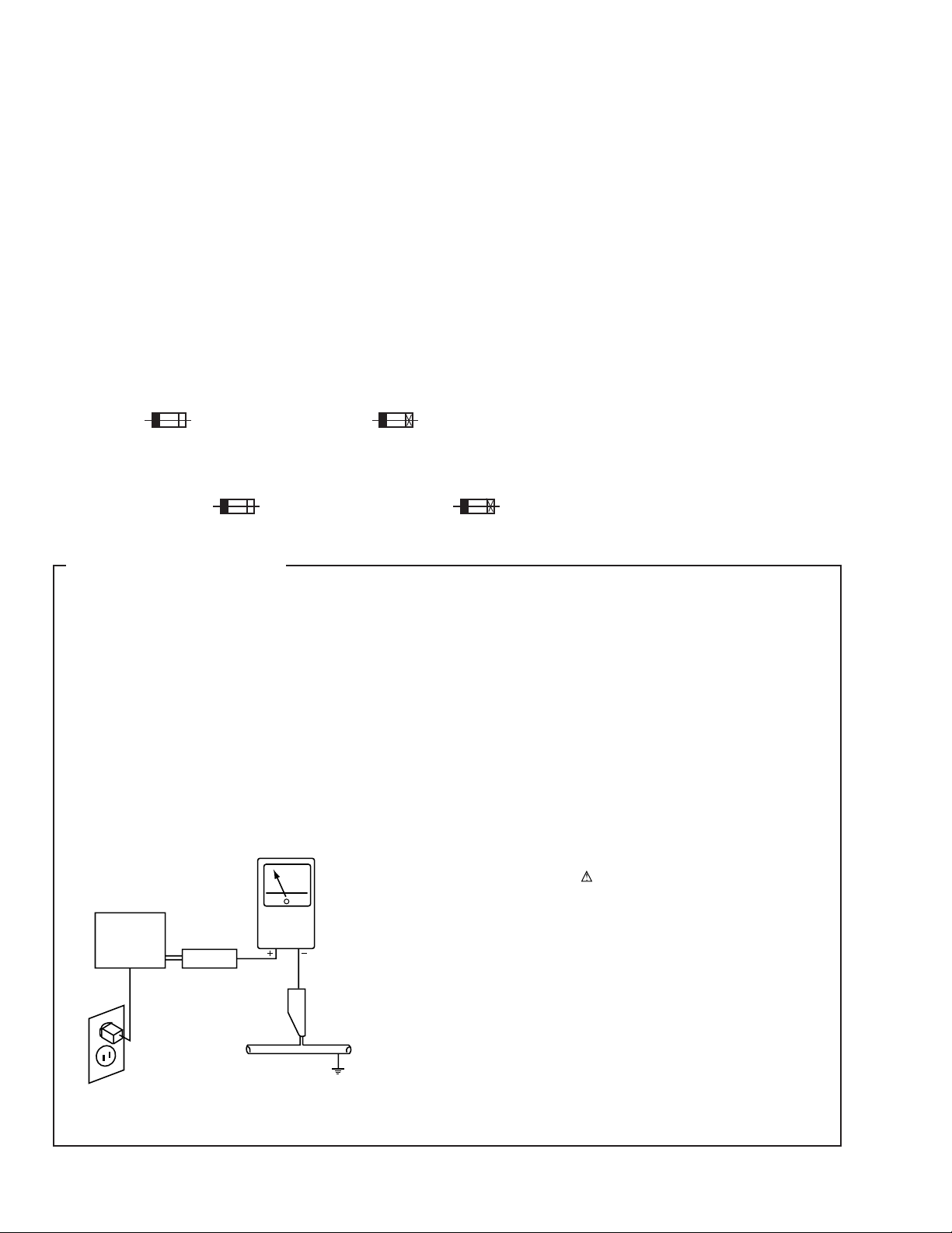
LEAKAGE CURRENT CHECK
Measure leakage current to a known earth ground (water
pipe, conduit, etc.) by connecting a leakage current tester
such as Simpson Model 229-2 or equivalent between the
earth ground and all exposed metal parts of the appliance
(input/output terminals, screwheads, metal overlays, control
shaft, etc.). Plug the AC line cord of the appliance directly
into a 120V AC 60Hz outlet and turn the AC power switch
on. Any current measured must not exceed 0.5mA.
Reading should
not be above
0.5mA
Earth
ground
Device
under
test
Also test with
plug reversed
(Using AC adapter
plug as required)
Leakage
current
tester
Test all
exposed metal
surfaces
ANY MEASUREMENTS NOT WITHIN THE LIMITS
OUTLINED ABOVE ARE INDICATIVE OF A POTENTIAL
SHOCK HAZARD AND MUST BE CORRECTED BEFORE
RETURNING THE APPLIANCE TO THE CUSTOMER.
2. PRODUCT SAFETY NOTICE
Many electrical and mechanical parts in the appliance
have special safety related characteristics. These are
often not evident from visual inspection nor the protection
afforded by them necessarily can be obtained by using
replacement components rated for voltage, wattage, etc.
Replacement parts which have these special safety
characteristics are identified in this Service Manual.
Electrical components having such features are identified
by marking with a
in this Service Manual.
The use of a substitute replacement component which does
not have the same safety characteristics as the PIONEER
recommended replacement one, shown in the parts list in
this Service Manual, may create shock, fire, or other hazards.
Product Safety is continuously under review and new
instructions are issued from time to time. For the latest
information, always consult the current PIONEER Service
Manual. A subscription to, or additional copies of, PIONEER
Service Manual may be obtained at a nominal charge from
PIONEER.
on the schematics and on the parts list
AC Leakage Test
2
Page 3
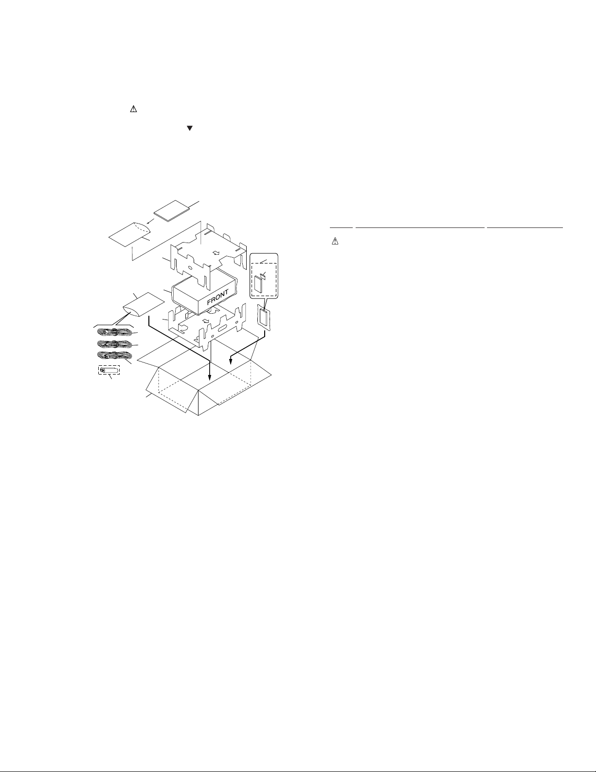
2. EXPLODED VIEWS AND PARTS LIST
NOTES:• Parts marked by "NSP" are generally unavailable because they are not in our Master Spare Parts List.
2.1 PACKING
The mark found on some component parts indicates the importance of the safety factor of the part.
•
Therefore, when replacing, be sure to use parts of identical designation.
Screws adjacent to mark on the product are used for disassembly.
•
DV-S6D
8
10
11
10
14
12
1
6
5
7
13
15
16
¶ PACKING PARTS LIST
Mark No. Description Part No.
1 Power Cord ADG7006
2 • • • • •
3 • • • • •
4 • • • • •
5 Audio Cord (L=1.5m) VDE1033
6 Video Cord (L=1.5m) VDE1034
NSP 7 Dry Cell Battery(R6P,AA) VEM-013
8 Operating Instructions VRD1091
(English/Trad-Chinese)
9 • • • • •
10 Polyethylene Bag VHL1051
(0.03×200×300)
11 Protector A VHB1065
12 Protector B VHB1076
13 Packing Case VHG1878
14 Mirror Mat Sheet VHL1012
15 Remote Control Unit VXX2628
(CU-DV037)
16 Battery Cover VNK4422
3
Page 4
DV-S6D
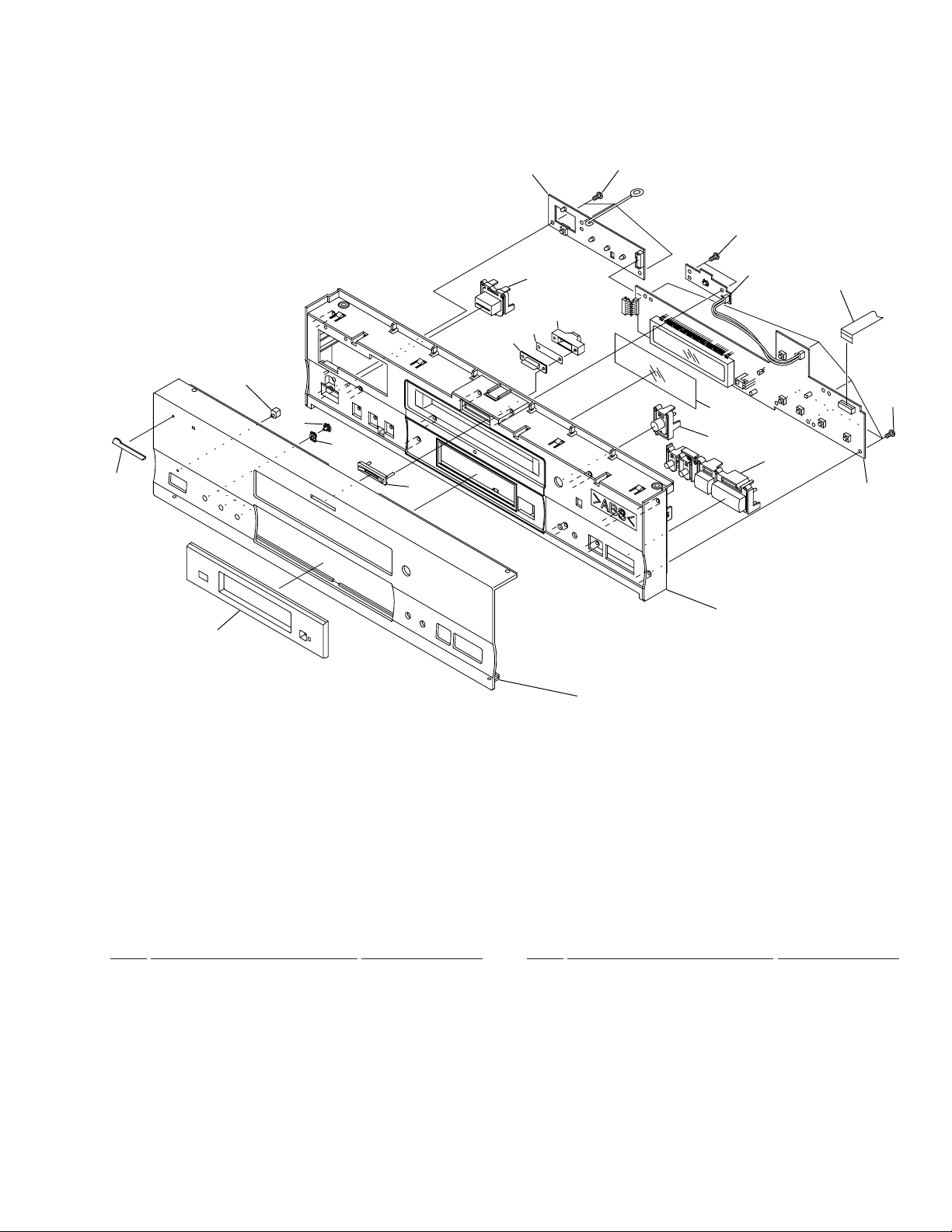
2.2 EXTERIOR SECTION
1
16
11
17
10
16
16
15
12
11
13
14
6
19
20
3
2
5
19
20
9
4
7
8
16
Refer to "2.3 FRONT PANEL SECTION".
¶ EXTERIOR SECTION PARTS LIST
Mark No. Description Part No. Mark No. Description Part No.
1 Bonnet S VXX2617
2 Door Panel VNK4524
3 DVD Plate VAM1077
4 Door Cushion VEC2103
5 Door Plate VEC2104
6 Tray VNK4333
7 Tray Stopper VNL1739
8 Tray Stopper Spring VBH1277
9 Door Holder VNK4325
10 Screw IBZ30P060FCC
NSP 17 Cord with Plug DE010VF0
11 Screw BCZ40P060FNI
12 Clamper Plate VNE2068
13 Bridge VNE2069
14 Clamper VNL1738
15 Screw BPZ26P080FZK
16 Screw BBZ30P080FMC
18 • • • • •
19 Screw VBA1057
20 Door Spring VBH1305
4
Page 5
2.3 FRONT PANEL SECTION
DV-S6D
2
8
12
13
14
11
15
5(2/3)
7
6
5(3/3)
10
17
9(1/2)
5(1/3)
10
3
16
10
9(2/2)
1
¶ FRONT PANEL SECTION PARTS LIST
Mark No. Description Part No.
1 FLKY Assy VWG2093
NSP 2 PWSB Assy VWG2098
NSP 3 DILB Assy VWG2100
4 Front Almi VAH1328
5 Panel Base VNK4323
6 FL Lens VEC2089
7 Name Plate PAN1377
8 PW Button (POWER) VNK4059
9 Main Key VNK4095
10 Screw BBZ30P080FMC
4
Mark No. Description Part No.
11 LED Lens PNW2019
12 Illumi Holder VNK4098
13 Illumination Filter VEC1950
14 Illumination Lens VNK4168
15 LED Lens VNK4326
16 Flexible Cable (15P) VDA1728
(FLKY CN101 ↔ DVDM CN602)
17 FL Filter VEC2016
5
Page 6
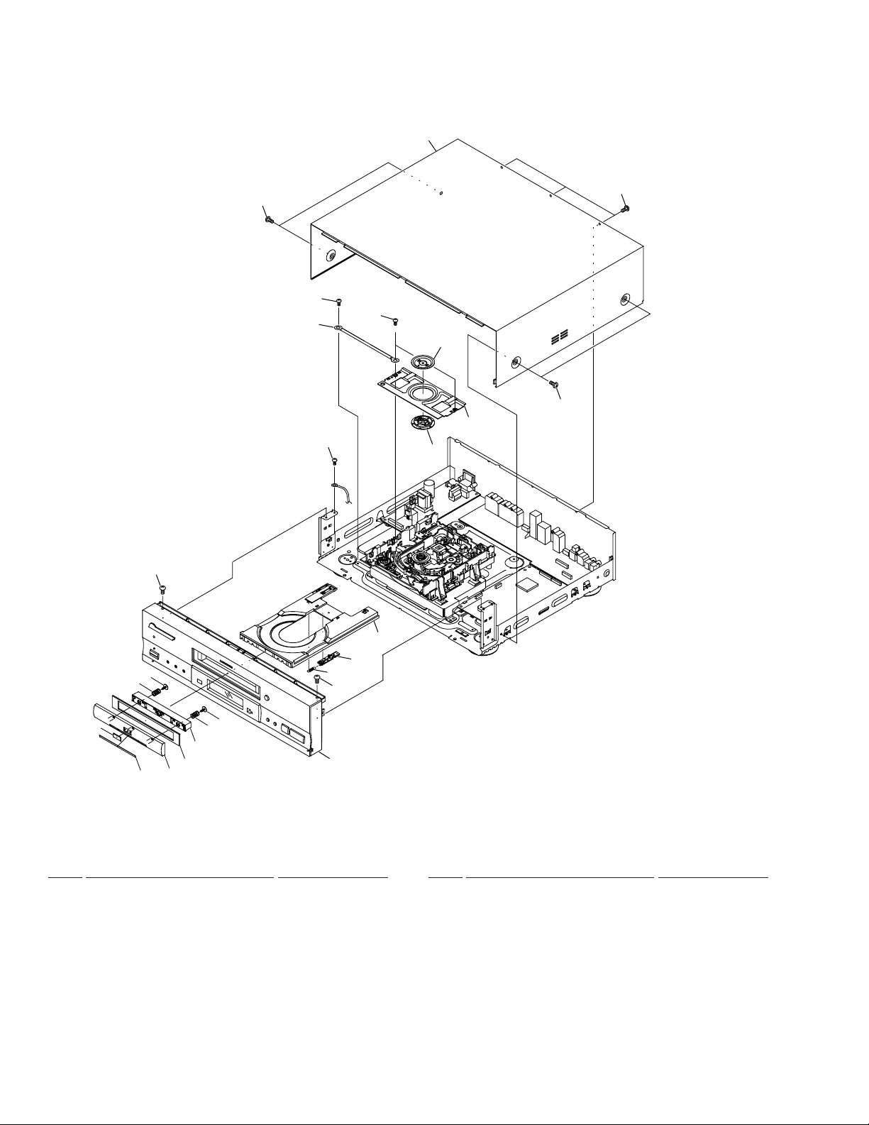
DV-S6D
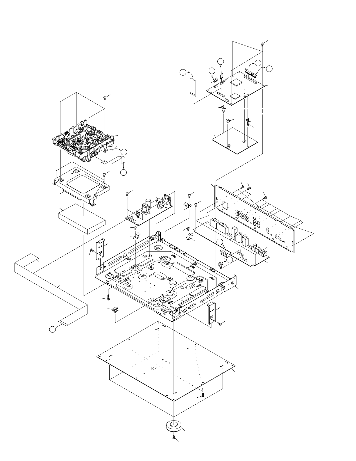
2.4 BOTTOM VIEW SECTION
38
33
36
39
7
Refer to
"2.5 LOADING MECHANISM ASSY".
E
38
A
38
38
32
34
4
38
35
E
38
32
38
17
A
9
29
30
6
23
C
B
11
C
D
12
1
29
23
23
38
10
22
21
34
38
D
16
2
B
31
38
18
37
6
Page 7

¶ BOTTOM VIEW SECTION PARTS LIST
Mark No. Description Part No.
1 DVDM Assy VWS1384
2 JCKB Assy VWV1682
3 • • • • •
4 POWER SUPPLY Assy VWR1316
5 • • • • •
DV-S6D
NSP 7 Loading Mechanism Assy VWT1164
NSP 16 Base Chassis VNA1979
NSP 22 PCB Holder PNW2029
6 VQEB Assy VWV1669
8 • • • • •
9 Flexible Cable (12P) VDA1692
(DVDM CN3 ↔ LOSB CN301)
10 Flexible Cable (26P) VDA1668
(DVDM CN2 ↔ POWER SUPPLY CN201)
11 Flexible Cable (29P) VDA1771
(DVDM CN905 ↔ JCKB CN666)
12 Flexible Cable (15P) VDA1772
(DVDM CN901 ↔ JCKB CN999)
13 • • • • •
14 • • • • •
15 • • • • •
17 Rear Panel VNA2113
18 Insulator PNW2766
19 • • • • •
20 • • • • •
21 PCB Hinge VEC1174
23 Screw BBZ30P080FMC
24 • • • • •
25 • • • • •
26 • • • • •
27 • • • • •
28 • • • • •
29 PCB Spacer VEC2077
30 PCB Support Cushion VEC2079
NSP 31 Bottom Plate PNA2376
NSP 32 PCB Base RNE1221
33 Mecha Cushion VEC2011
NSP 34 Panel Stay VNE2156
NSP 35 Stay VNE2214
NSP 36 Mecha Holder VNE2220
37 Screw ABZ30P080FMC
38 Screw IBZ30P060FCC
39 Screw BBZ30P100FMC
7
Page 8
DV-S6D
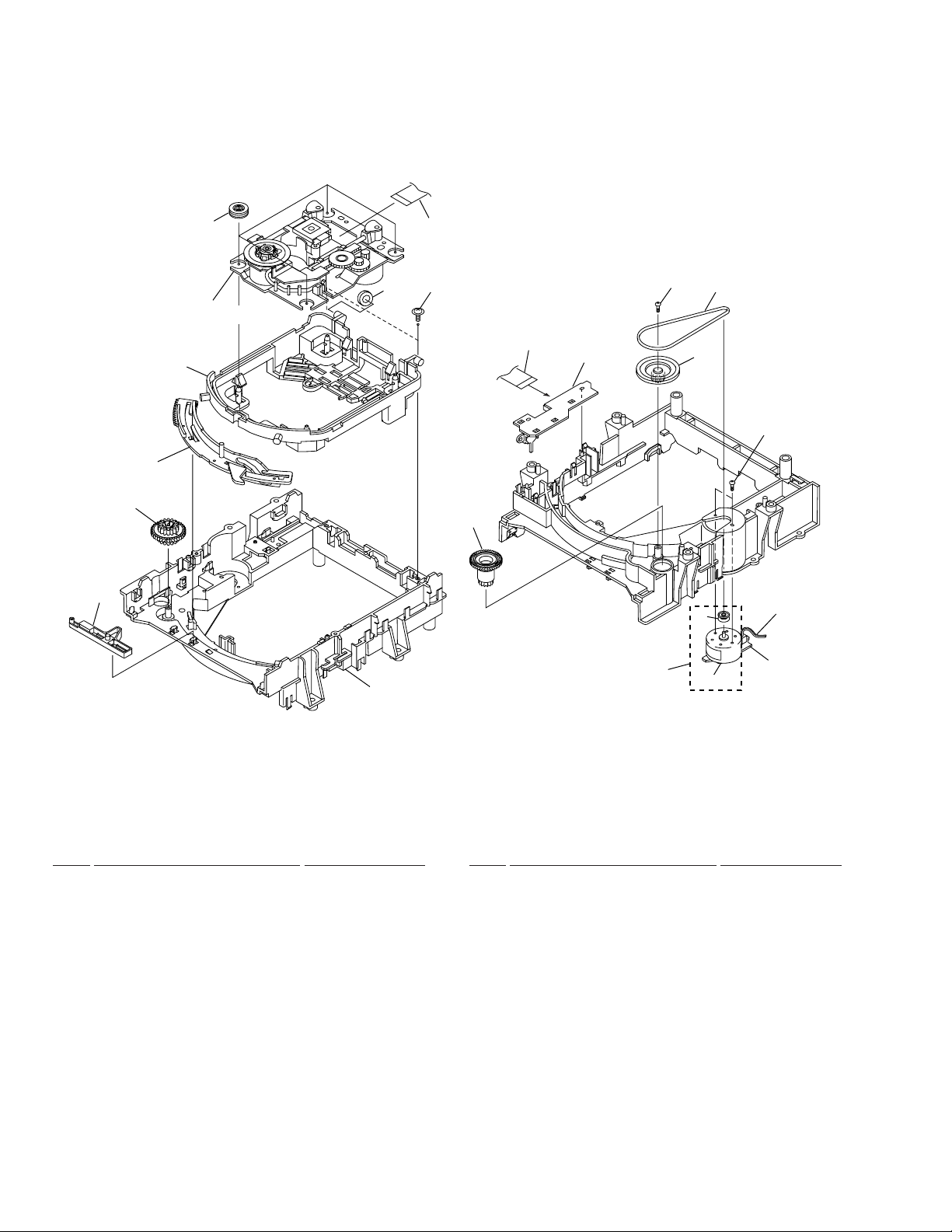
2.5 LOADING MECHANISM ASSY
• Top View • Bottom View
20
Refer to
"2.6 TRAVERSE MECHANISM ASSY-S".
3
4
5
1
19
21
11
17
13
7
8
16
15
14
12
2
22
18
10
6
9
¶
LOADING MECHANISM ASSY PARTS LIST
Mark No. Description Part No. Mark No. Description Part No.
1 Traverse Mechanism Assy-S VXX2653
2 Screw DBA1006
3 Drive Cam VNL1736
4 Drive Gear VNL1735
5 Lock Plate VNL1820
6 Loading Base VNL1730
7 Belt VEB1260
8 Gear Pulley VNL1733
NSP 9 LOSB Assy VWG1885
10 Loading Gear VNL1734
NSP 14 LOMB Assy VWG1886
11 Loading Motor Assy VXX2505
12 DC Motor / 0.3W PXM1027
13 Motor Pulley PNW1634
15 Connector Assy VKP2198
(LOMB CN401 ↔ LOSB CN303)
16 Screw VBA1055
17 Screw Z39-019
18 Flexible Cable (08P) VDA1698
(LOSB CN302 ↔ SMEB CN202)
19 Float Base VNL1815
20 Floating Rubber VEB1286
21 Flexible Cable (24P) VDA1701
(Pickup Assy ↔ DVDM CN4)
22 Cushion VEB1312
8
Page 9
2.6 TRAVERSE MECHANISM ASSY-S
• Top View
DV-S6D
37
37
17
31
24
30
16
35
33
28
5
22
33
21
15
10
10
14
10
23
7
2
7
34
19
8
6
20
12
9
37
4
10
13
37
18
32
1
18
26
11
25
27
7
29
36
3
¶
TRAVERSE MECHANISM ASSY-S PARTS LIST
Mark No. Description Part No. Mark No. Description Part No.
NSP 1 SMEB Assy VWG2048
NSP 2 FGSB Assy VWG2009
NSP 3 Motor VXM1079
NSP 4 Motor VXM1078
NSP 5 Pickup Assy VWY1055
6 Table Sheet DEC2040
7 Screw VBA1058
8 Centering Spring VBH1278
9 Hook Spring VBH1317
10 Skew Spring VBH1303
11 Gear Spring VBH1308
NSP 12 Reflected Sheet VEC1959
13 Guide Bar VLL1504
14 Sub-guide Bar VLL1505
15 Hold Spring VNC1017
NSP 16 Magnet Holder VNE2070
NSP 17 Motor Base VNE2154
NSP 18 Cover VNE2155
19 Centering Ring VNL1746
NSP 20 Disc Table VNL1747
NSP 30 Magnet VYM1024
21 Hook VNL1770
22 FFC Holder VNL1802
23 Mechanism Base VNL1806
24 FG Holder VNL1807
25 Gear A VNL1808
26 Gear B VNL1809
27 Gear C VNL1810
28 Slider VNL1811
29 Gear D VNL1814
31 Screw JFZ17P025FZK
32 Screw JGZ17P028FMC
33 Screw VBA1051
34 Magnet Holder Assy VXX2507
35 Spindle Motor Assy VXX2649
36 Carriage Motor Assy VXX2650
37 Screw PBA1069
9
Page 10
1
23
DV-S6D
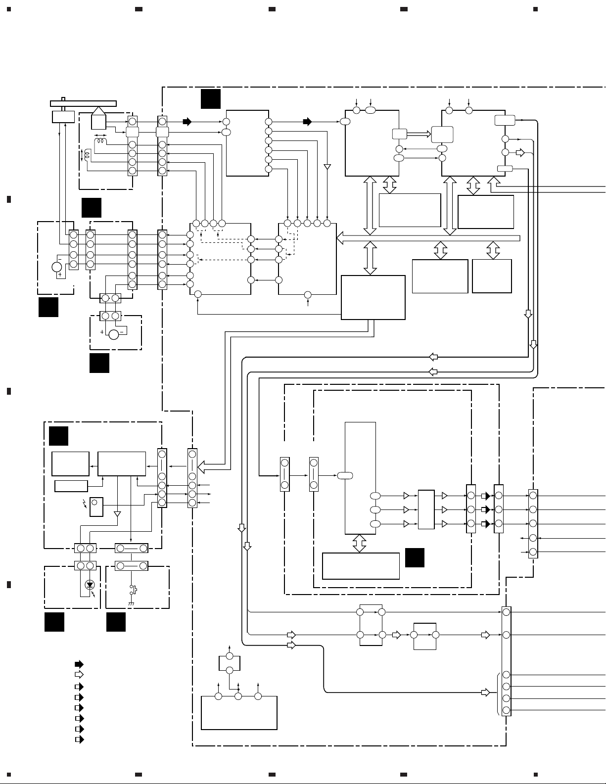
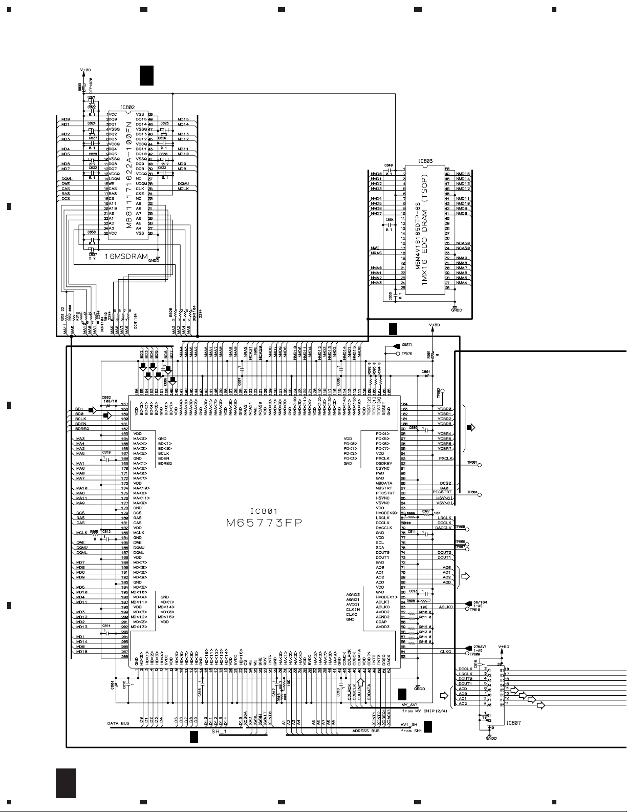
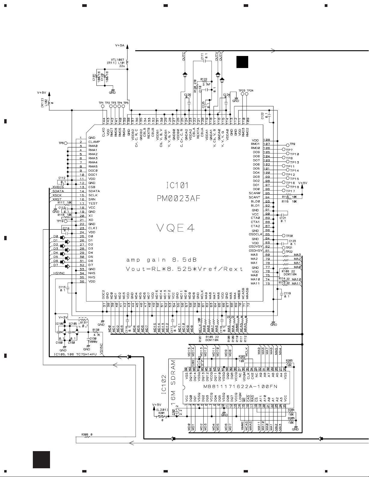
3. BLOCK DIAGRAM AND SCHEMATIC DIAGRAM
3.1 BLOCK DIAGRAM
4
33M
A
SPDL
MOTOR
FCS
OEIC
TRKG
PICKUP
(24P)
10
7,6,
3,2
21
24
22
23
F_RTN
F_DRV
T_DRV
T_RTN
CN120
10
7,6,
3,2
21
24
22
23
(24P)
E
DVDM ASSY
RFRF
3 54
6-9
LA9701M
RF IC
IC101
B1-B4
46
56
57
42
35
RFO
DSPRF
BH
PH
FE
TE
Q105
4
170
DECODER
PD4995A
16M
107
DVD
MY CHIP
IC701
57-60
63-66
56
111
SD0-SD7
SREQ
CDDATA
149,150,
152-155,
158,159
162
48
27M
36/16M
55 64
DECODER
MITUBISHI
M65773FP
MPEG2
AV-1
IC801
95-98,
100-103
74
73
68-71
YCBR0-7
(Y0-Y7)
DOUT0
DOUT1
AD0-2,
ADD
ASSY
LOSB
B
ASSY
CN302
(8P)
2
7
1
8
4
5
6
3
M
CN202
(8P)
CARRIAGE
B
MOTOR
C
SMEB
ASSY
LOADING MOTOR
A
(12P)
CN301
8
10
6
4
7
9
12
CN303
CN401
21
M
LOMB
ASSY
SPDL+
SPDL-
SLDR_R
SLDR_F
LOAD+
LOAD-
(12P)
CN1030
5
3
7
9
6
4
13 12 10 9
31
32
14
15
SPDL & FTS
34
35
M56788FP
37
LODDRV
DRIVER
IC352
32 33 30 31 39
FDO
3
47
TDO
48
20
SLDO
17
45
SERVO DSP
46
IC201
LC78652W
14
16M
SYSTEM
CONTROL CPU
SH1 BASE ASIC
IC601
PD3410A
SPDO
28
4M DRAM
IC702
MN414800CSJ-07
WORK SRAM
TC55V1001AF8
(1M)
IC604
16M SDRAM
IC802
MB811171622A
-100FN
FLASH
MEMORY
IC603
VYW1669
VIDEO ENCODER
(6ch, DNR)
IC101
PM0023AF
SEL IR
IR
(15P)
CN602
1
12
SEL IR
13
IR
14
SW+5V
15
16M
5
1
27M
33M
6
5
CLOCK GENERATOR
IC21
CY2081SL-655
CN801
-1/2
7
(Y0-Y7) D0-D7
DOUT0
DOUT1
IC22
TC7WH74FU
36/16M
1
D0-D7
14
DNR
CN101
-1/2
27
25-32
34
16M SDRAM
MB811171622A-100FN
TC74VHCT541ADT
IC102
4 16
IC807
117
115
125
OUTV
OUTY
OUTC
Q541
Q551
Q531
F
LC89051V
VIDEO
FILTER
F102
VQEB
ASSY
1155 23
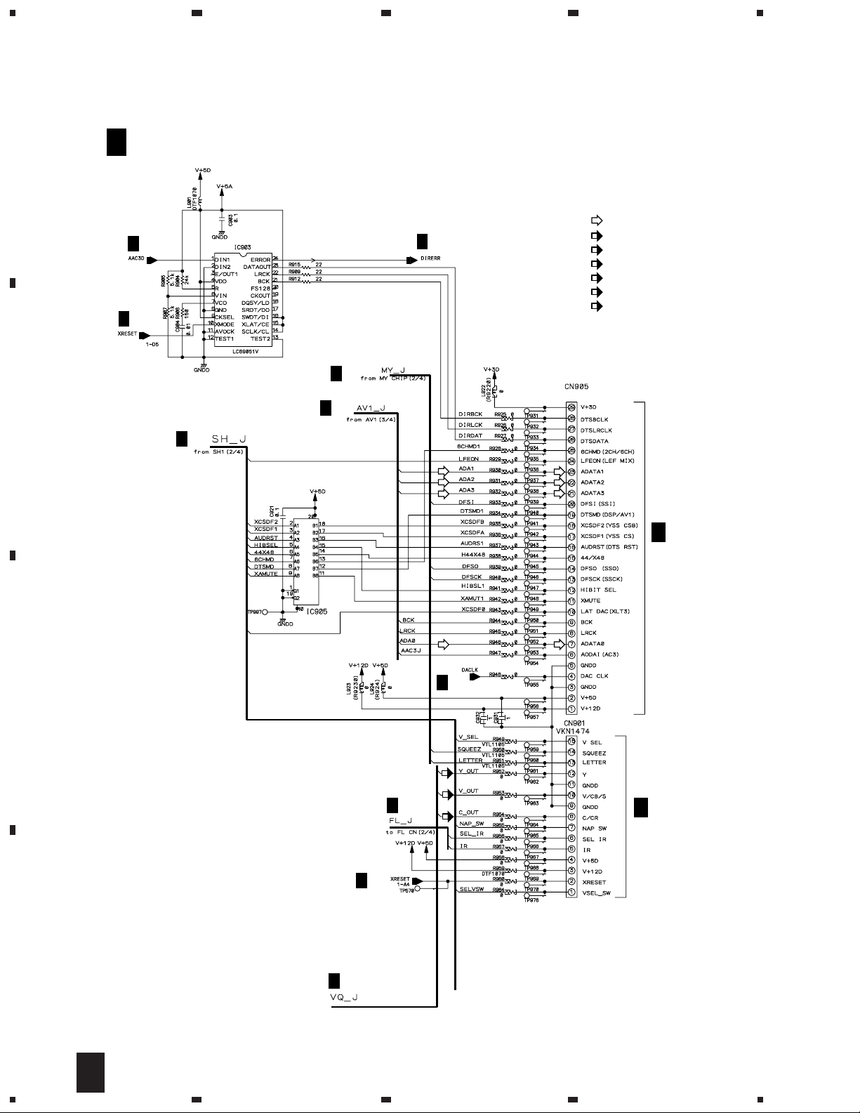
DIR
IC903
Q542
Q552
Q532
(15P)
22
24
26
CN901
SEL IR
V
Y
C
IR
(22P)
10
12
8
6
5
(V)
2
(Y)
4
(C)
6
CN905
ADATA1
6
DTSDATA
26
ADATA1
23
ADATA2
22
ADATA3
21
ADATA0
7
CN102
1 7
(15P)
CN101
(7P)
15
4
3
2
1
H
FLKY ASSY
FL TUBE
V101
VAW1050
C
KEY SW
REMOTE
SENSOR
FL CONTROL
IC101
PE5141A
J101
12
J301
J
12
DILB
ASSY
1 7
I
(7P)
CN201
PWSB
ASSY
: RF Signal Route
D
: Audio Signal Route (L ch)
(V)
: V Signal Route
(Y)
: Y Signal Route
(C)
: C Signal Route
(R)
: R Signal Route
(G)
: G Signal Route
(B)
: B Signal Route
10
1234
Page 11
5
678
DV-S6D
CN110
M + 6V
+12V
+12V
+5V
+3.3V
EV+5V
– 27V
EDO DRAM
IC803
M5M4V18165
DTP-6S
(26P)
(26P)
1,2
10
12
13
16
CN201
1,2
5
5
7
7
10
|
|
12
13
|
|
16
22
22
26
26
POWER
L
SUPPLY
ASSY
CN101
LIVE
1
2
NEUTRAL
AC IN
A
B
G
(15P)
CN999
6
4
8
JA904
10
11
24
4 84
7
8
9
23
(29P)
CN666
IC666
11
SR OUT
JA903
SR IN
9
10
JCKB ASSY
IC902
DTS
DECODER
IC501
YSS912C-F
5
7
6
SELECTOR
IC404,IC405,IC666
TC74VHC157FT
IC901
(V) (V)
3
(Y)
(C)
10
6
VIDEO
AMP
IC801
LA7135M
23
15
19
13
21
17
OPTICAL AC-3/PCM
COAXIAL
29
28
96k,24bit
6ch DAC
IC401
UDA1328T/S1
1
2
4
(Y)
DIGITAL
AUDIO
OUT
2
NJM5532MD
3
2
3
5
6
2
BA4560F
3
(C)
IC301
1
1
IC101
BA4560F
7
IC201
1
R ch
R ch
Q805,
Q806
Q705,
Q706
Q715,
Q716
(V)
(Y)
(C)
(Y)
(CB)
(C
R)
JA301
JA101
JA801
COMPOSITE
VIDEO OUT
(Y)
(C)
Y
ANALOG
COMPONENT
PB
VIDEO
OUT
PR
JA601
Lt1
Lt2
Rt1
Rt2
FRONT L
FRONT R
CENTER
SUB WOOFER
R SURROUND
L SURROUND
JA701
S VIDEO
OUTPUT
C
D
11
5
6
7
8
Page 12
1
23
4
DV-S6D
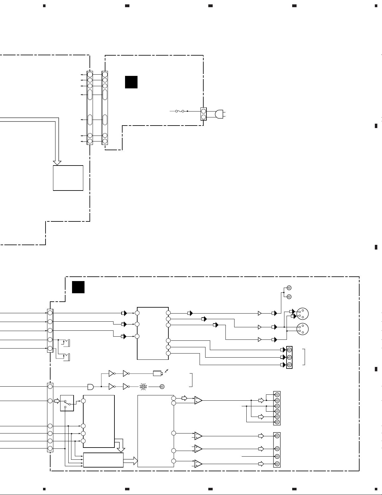
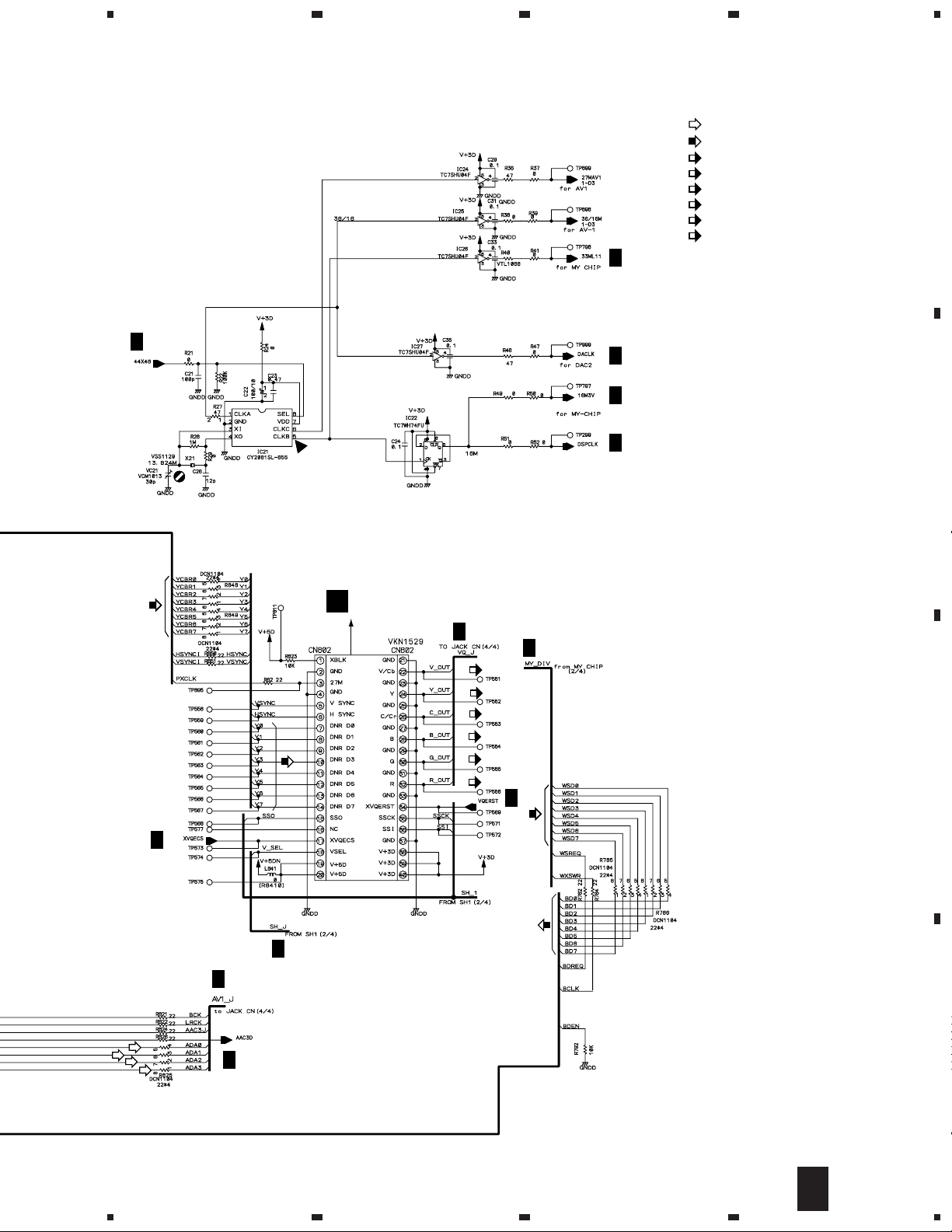
3.2 LOMB, LOSB, SMEB, FGSB ASSYS and OVERALL WIRING DIAGRAM
A
Note : When ordering service parts, be sure to refer to "EXPLODED VIEWS and PARTS LIST" or "PCB PARTS LIST".
B
G
G 1/2, G 2/2
JCKB ASSY
(VWV1682)
C
J101J301
J
DILB ASSY
(VWG2100)
D
I
PWSB ASSY
5.1ch MODE
FL_OFF
DNR_ON
(VWG2098)
H
FLKY ASSY
(VWG2093)
77
12
1234
Page 13
5
678
DV-S6D
A
E
E 1/4- E 4/4
DVDM ASSY
(VWS1384)
F
VQEB ASSY
(VWV1669)
POWER SUPPLY ASSY
(VWR1316)
(T)
(F)
(F)
(F)
(F)
(T) (T)
CN301
VKN1272
(F)
(F)
L
(T)
PICKUP
ASSY
(VWY1055)
S301
VSK1011
CN302
VKN1268
AC110V 60Hz
AC POWER CORD
ADG7006
: RF SIGNAL ROUTE
(F)
: FOCUS SERVO LOOP LINE
(T)
: TRACKING SERVO LOOP LINE
(S)
: SLIDER SERVO LOOP LINE
FGSB ASSY
D
(VWG2009)
PC101
TLP910(O)
CN202
VKN1212
S201
DSG1016
R101
680
CN201
52044-0345
B
C
CN101
5
CN101
(S)
(S)
LOSB ASSY
B
(VWG1885)
LOMB ASSY
A
(VWG1886)
6
CN303
B2B-PH-K-S
CN401
B2B-PH-K-S
LOADING MOTOR
ASSY
(VXX2505)
7
(S)
(S)
(S)
(S)
CARRIAGE MOTOR
ASSY
(VXX2650)
(SLIDER)
C
SMEB
ASSY
(VWG2048)
D
SPINDLE MOTOR
ASSY
(VXX2649)
DCBA
8
13
Page 14
1
DV-S6D
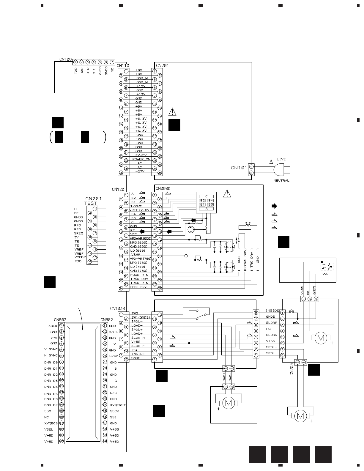
3.3 DVDM ASSY (1/4)
23
4
E 1/4
A
CN110
VKN1479
B
DVDM ASSY (VWS1384)
1
E
2/4
E
2/4
E
2/4
E
2/4
(DVD) (DVD)
E
2/4
(CD)
(DVD)
(CD)
(CD)
(F)
CN201
VKN1324
2
4
CN201
E
L
2/4
(F)
E
2/4
(F)
(F)
(T)
(T)
CN120
VKN1484
C
(T)
(F)
(F)
E
(F)
(T)
2/4
PICKUP ASSY
(F)
(T)
(T)
(F)
CN1030
VKN1471
E
2/4
(T)
(T)
IC352 :
SPDL & FTS
DRIVER
(T) (T)
E
E
2/4
2/4
E
2/4
E
2/4
D
CN301
B
14
1/4
E
1234
(S)
(F)
(F)
(T)
(T)
(S)
(S)
E
2/4
(F)
(S)
(T)
(S)
Page 15
5
678
DV-S6D
(DVD)
(DVD)
: The power supply is shown with the marked box.
: RF SIGNAL ROUTE
: ROM DATA SIGNAL ROUTE
(F)
: FOCUS SERVO LOOP LINE
(T)
: TRACKING SERVO LOOP LINE
(S)
: SLIDER SERVO LOOP LINE
E
2/4
FOR CHECKER
E
3/4
6
R1 R2 R3 R4
LB − 10k − 10k
E
2/4
E
2/4
A
B
(CD) (CD)
(S)
(F)
(T)
E
2/4
E
7
2/4
5
C
IC751
E
2/4
8
E
E
2/4
4/4
9
10
11
E
2/4
E
2/4
E
2/4
D
1/4
E
5
6
7
8
15
Page 16
1
DV-S6D
3.4 DVDM ASSY (2/4)
23
4
A
E 2/4
VYW1669
B
E
4/4
DVDM ASSY (VWS1384)
TC55V1001AF8
E
1/4
E
4/4
3 TO 5
CONVERTER
MC74VHCT541ADT
E
3/4
5 TO 3
CONVERTER
MC74VHCT541DT
E
1/4
E
3/4
E
3/4
E
4/4
(V_SEL)
X601
20MHz
DSS1110
C
E
3/4
E
E
E
1/4
E
1/4
E
1/4
D
E
1/4
E
1/4
E
E
1/4
E
1/4
3/4
E
1/4
E
4/4
1/4
1/4
E
1/4
RB521S-30
E
1/4
E
3/4
RB521S-30
16
2/4
E
1234
Page 17
5
678
DV-S6D
: The power supply is shown with the marked box.
: AUDIO SIGNAL ROUTE
: ROM DATA SIGNAL ROUTE
A
MN414800CSJ-07
E
2/4
E
3/4
DVD ENCODER
E
4/4
E
3/4
E
4/4
B
E
1/4
E
1/4
E
1/4
E
1/4
3
E
3/4
E
3/4
E
1/4
E
1/4
E
1/4
CN101
H
E
3/4
E
E
1/4
1/4
C
D
2/4
E
5
6
7
8
17
Page 18
1
DV-S6D
3.5 DVDM ASSY (3/4)
23
4
E 3/4
A
B
DVDM ASSY (VWS1384)
E
2/4
100/10
C
MPEG2 DECODER
MITSUBISHI AV1
3 - 5 CONVERTER
100/10
D
E
2/4
18
3/4
E
1234
E
2/4
E
2/4
TC74VHCT541ADT
Page 19
5
678
DV-S6D
: AUDIO SIGNAL ROUTE
: ROM DATA SIGNAL ROUTE
(V)
: VIDEO SIGNAL ROUTE
(Y)
: Y SIGNAL ROUTE
(C)
: C SIGNAL ROUTE
(R)
: R SIGNAL ROUTE
(G)
: G SIGNAL ROUTE
(B)
: B SIGNAL ROUTE
E
2/4
E
2/4
CLOCK GENERATOR
E
4/4
E
2/4
E
1/4
A
B
CN101
F
E
4/4
E
(V)
(Y)
(C)
(B)
(G)
(R)
E
2/4
E
2/4
E
4/4
2/4
C
E
2/4
E
4/4
3/4
E
5
6
7
8
19
D
Page 20
1
DV-S6D
3.6 DVDM ASSY (4/4)
23
4
A
E 4/4
E
B
DVDM ASSY (VWS1384)
E
2/4
3/4
E
2/4
DIR
3 TO 5 CONVERTER
: AUDIO SIGNAL ROUTE
(V)
: VIDEO SIGNAL ROUTE
E
2/4
E
2/4
E
3/4
(Y)
(C)
(R)
(G)
(B)
VKN1585
: Y SIGNAL ROUTE
: C SIGNAL ROUTE
: R SIGNAL ROUTE
: G SIGNAL ROUTE
: B SIGNAL ROUTE
G1/2
CN666
MC74VHCT541ADT
E
C
E
2/4
3/4
(Y)
(V)
(C)
G2/2
CN999
E
1/4
D
E
3/4
20
4/4
E
1234
Page 21

DV-S6D
21
Page 22
1
VQEB ASSY
(VWV1669)
F
(6 ch, DNR) VIDEO ENCODER
(C) (V)
(Y)
DV-S6D
3.7 VQEB ASSY
A
B
23
4
C
D
22
F
1234
Page 23
5
678
DV-S6D
: The power supply is shown with the marked box.
A
B
14 17
,
12 15
,
13 16
,
E 3/4
CN802
(V)
(C)
(V)
(Y)
(C)
(V)
(Y)
(Y)
(C)
(B)
(G)
(R)
C
: ROM DATA SIGNAL ROUTE
(V)
: VIDEO SIGNAL ROUTE
(Y)
: Y SIGNAL ROUTE
(C)
: C SIGNAL ROUTE
5
6
7
(R)
: R SIGNAL ROUTE
(G)
: G SIGNAL ROUTE
(B)
: B SIGNAL ROUTE
F
8
D
23
Page 24
1
DV-S6D
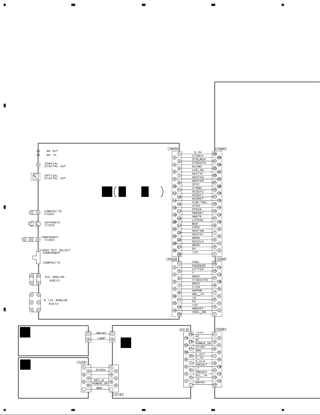
3.8 JCKB ASSY (1/2)
23
4
G 1/2
A
CN905
JCKB ASSY (VWV1682)
G
2/2
E 4/4
B
IC401 :
96k, 24 bit
6 ch DAC
C
DTS DECODER
D
24
1/2
G
1234
Page 25
5
678
DV-S6D
UDZS6.2B
: AUDIO SIGNAL ROUTE
A
B
UDZS6.2B
TC4W53F
C
D
: The power supply is shown with the marked box.
1/2
G
5
6
7
8
25
Page 26
1
DV-S6D
3.9 JCKB ASSY (2/2)
23
4
G 2/2
A
B
JCKB ASSY (VWV1682)
G
1/2
CN901
(V)
(Y)
(V)
(C)
(Y) (Y)
(V)
(C)(C)
E 4/4
C
D
26
2/2
G
1234
Page 27

5
678
DV-S6D
: The power supply is shown with the marked box.
: AUDIO SIGNAL ROUTE
(V)
: VIDEO SIGNAL ROUTE
(Y)
: Y SIGNAL ROUTE
(C)
: C SIGNAL ROUTE
A
(V)
(V)
(V)
VIDEO AMP
(V)
(C)
(C)
(Y)
(V)
(Y)
(Y)
(Y)
(C)
(C)
(C)
(C)
(Y)
(C)
B
(C)
(Y) (Y)
(CB) (CB)
(CR) (CR)
5
6
7
(PB)
(PR)
G
2/2
8
27
C
D
Page 28

1
23
DV-S6D
3.10 FLKB, PWSB and DILB ASSYS
4
A
B
FLKY ASSY
H
(VWG2093)
R141 R143
LB 47k 62k
C
D
28
H
1234
Page 29

5
678
DV-S6D
PWSB ASSY
I
(VWG2098)
A
B
CN602
E 2/4
FLKY ASSY
S101 : ¡¢ (FORWARD)
S102 : 41 (REVERSE)
S103 : 7 (STOP)
S105 : 0 (OPEN/CLOSE)
S106 : 3 (PLAY)
: The power supply is shown with
the marked box.
J
DILB ASSY
(VWG2100)
PWSB ASSY
S201 : STANDBY/ON(POWER)
C
D
IH
5
6
7
J
8
29
Page 30

1
DV-S6D
3.11 POWER SUPPLY ASSY
A
NOTE OF SPARE PARTS IN POWER SUPPLY (SYPS) ASSY
• In case of repairing, use the described parts only to prevent an accident.
• Please write the red mark on the board when the primary section of POWER SUPPLY (SYPS) Assy is repaired.
• Please take care to keep the space, not touching other parts when replacing the parts.
POWER SUPPLY ASSY (VWR1316)
K
C112
D108
VZF1045
23
4
T101
7
9
1
2
3
5
6
10
11
14
12
GND2
13
16
15
T102
10
8
D106
(1/2)
VZF1071
D110
1SS270A
C121
6
5
4
2
1
Q103
VZF1062
R105
CN101
YKE31-0120
1
AC IN
2
R130
R131
LIVE
NEUTRAL
C111
C120
Q101
VZF1062
C117
R110
F101
2A/125V (REK1078)
F101
C101
R101
C104
D103
VZF1077
L101
413
C103
C105
FG101
C122
D107
1SS270A
2SC1740S
2
B
C
Q104
C102
R120
R108
R109
D109
(1/2)
VZF1071
D101
VZF1044
C110
Q102
2SC3377
D152
C153
S
BP FB
C154
L104
L103
C116
D104
MTZJ2.4B
C115
SD
IC151
SS
D153
R111
R151
D151(1/2)
VZF1071
R112R113
R116
D120
D105
1SS270A
C151
D102
EG01C
R114
D
30
C107 C108
K
1234
Page 31

5
678
DV-S6D
A
VZF1065
VZF1065
VZF1076
VZF1075
D811
VZF1054
D211
D711
D311
D411
D412
D511
10ELS2
D611
D213
MTZJ15B
C311
330/35
R511
33
VZC1057
P611
VEK1041
1.0A/60V
C411
330/35
C211
330/35
C711
330/35
D106
(2/2)
VZF1071
IC201
AN1431T
L811
L711
39µH/1.3A
R201
L211
39µH/1.3A
47
R202
1k
C201
0.47/50
R711
0.51 1/2W
VZC1061
R203
1.5k
R204
330
R205
1.5k
IC311
VZF1078
IIO
GCT
IC411
VZF1074
GCT
D513
MTZJ8.2B
O
R412
680
C412
100/35
R514
10k
R411
1.2k
C212
100/35
C511
47/50
P211
VEK1041
1.0A/60V
C313
47/35
CN201
52806-2610
1 M+6V
M+6V
2
GND (M+6V, M+12V)
3
GND (M+6V, M+12V)
4
M+12V
5
GND (D+12V)
6
D+12V
7
GND (+5V)
8
GND (+5V)
9
+5V
10
+5V
11
+5V
12
+3.3V
13
+3.3V
14
+3.3V
15
+3.3V
16
GND
17
GND
18
GND
19
GND
20
GND
21
22
EV. +5V
P ON/OFF
23
FLAC
24
FLAC
25
-27V
26
B
CN110
1/4
E
C
C811
330/35
D151
(2/2)
VZF1071
IC801
AN1431T
R801
47
R802
1k
C801
0.47/50
R803
1.5k
R804
100
R805
1.5k
D109
(2/2)
VZF1071
Q801
R806
680
C611
0.01/50
C812
330/35
C612
0.01/50
D
K
5
6
7
8
31
Page 32

DV-S6D
WAVEFORMS
Note : The encircled numbers denote measuring point in the schematic diagram.
Measurement condition : No. 1 to 4 and 6 to 11 : Disc MA1, Title 1-chp 1
No. 5 : CD, ABEX-784 Track 1
No. 12 to 14 : MJK1, Title 1-chp 4 or T2-1
No. 15 to 17 : MJK1, Title 1-chp 5 or T2-19
DVDM ASSY
Foot of R169 (RF)
1
V: 100mV/div. H: 0.2µsec/div.
CN201 - pin 5, 6 (RFO)
2
V: 500mV/div. H: 0.1µsec/div.
IC701 - pin 170 (MY CHIP input)
3
V: 1V/div. H: 0.2µsec/div.
GND
GND
GND
Q281 - Collector (FG)
7
V: 1V/div. H: 5msec/div.
Foot of R261 (FPWM)
8
V: 1V/div. H: 5msec/div.
Foot of R262 (VPWM)
9
V: 1V/div. H: 5msec/div.
GND
GND
GND
VQEB ASSY
Q541 Base (Composite Video output)
12
V: 0.1V/div. H: 10µsec/div.
Q551 Base (Y output)
13
V: 0.1V/div. H: 10µsec/div.
Q531 Base (C output )
14
V: 0.1V/div. H: 10µsec/div.
GND
GND
GND
Q501 Base
18
(R output when select RGB)
V: 0.1V/div. H: 10µsec/div.
Q521 Base
19
(G output when select RGB)
V: 0.1V/div. H: 10µsec/div.
Q511 Base
20
(B output when select RGB)
V: 0.1V/div. H: 10µsec/div.
GND
GND
GND
CN201 - pin 9, 10 (Tracking Error)
4
(AI-Inner Tracking Off)
V: 500mV/div. H: 2msec/div.
IC201 - pin 39 (EFM before slice)
5
V: 1V/div. H: 1µsec/div.
IC201 - pin 1 (EFM)
6
V: 1V/div. H: 0.2µsec/div.
GND
GND
Foot of R263 (PPWM)
10
V: 1V/div. H: 5msec/div.
Foot of R264 (RPWM)
11
V: 1V/div. H: 5msec/div.
GND
GND
Q541 Base (C
15
color difference output)
V: 0.1V/div. H: 10µsec/div.
Q551 Base (Y output when selecting
16
color difference output)
V: 0.1V/div. H: 10µsec/div.
Q531 Base (CR output when selecting
17
color difference output)
V: 0.1V/div. H: 10µsec/div.
B output when selecting
GND
GND
32
Page 33

1
234
4. PCB CONNECTION DIAGRAM
DV-S6D
NOTE FOR PCB DIAGRAMS :
1. Part numbers in PCB diagrams match those in the schematic
diagrams.
2. A comparison between the main parts of PCB and schematic
diagrams is shown below.
Symbol In PCB
Diagrams
BCE
BCE
D
Symbol In Schematic
Diagrams
BCEBCE
BCE
DGGSS
BCE
DGS
Part Name
Transistor
Transistor
with resistor
Field effect
transistor
Resistor array
3-terminal
regulator
3. The parts mounted on this PCB include all necessary parts for
several destinations.
For further information for respective destinations, be sure to
check with the schematic diagram.
4. View point of PCB diagrams.
4.1 LOMB, LOSB, SMEB and FGSB ASSYS
Connector
P.C.Board
Capacitor
Chip Part
A
SIDE A
SIDE B
B
LOSB ASSY
B
(VNP1628-A)
CARRIAGE
MOTOR
M
(VNP1695-A)
SMEB ASSY
C
CN1030
E
M
SPINDLE
MOTOR
PC101
R101
LOMB ASSY
A
(VNP1628-A)
D
LOADING
MOTOR
FGSB ASSY
C
(VNP1661-B)
D
SIDE A
DCBA
1
2
3
4
33
Page 34

1
DV-S6D
4.2 DVDM ASSY
23
• This PCB is a four-layered board.
4
A
B
PICKUP
ASSY
DVDM ASSY
E
G
CN666
G
CN999
IC23
IC26
IC31
IC25
IC54
Q809 Q807 Q811
IC21
IC801
VR851
VC21
IC22
IC903
IC261
IC302
IC807
Q810 Q808
Q812
IC806
IC303
IC702
C
D
B
CN301
CN201
L
H
CN101
(VNP1706-B)
IC610
Q111
Q107
Q112
IC101 IC601
Q102
IC761
Q281
IC352 IC603
IC606
Q601
Q602
34
SIDE A
E
1234
Page 35

1
234
DV-S6D
• This PCB is a four-layered board.
F
CN101
DVDM ASSY
E
IC905
IC803
IC27
IC805
IC802
IC201
IC701
A
IC73
B
SIDE B
(VNP1706-B)
Q542
IC608
Q106
IC299
Q543
IC904
IC609
IC611
IC612
IC751
IC792
IC604
IC607
IC231
Q179
Q105 Q237
Q113
Q114
Q101
Q103
IC791
C
Q106
Q251
D
E
1
2
3
4
35
Page 36

1
DV-S6D
4.3 VQEB ASSY
23
4
A
VQEB ASSY
F
SIDE A
B
VR102
VR101
Q551 Q541
Q531
Q521 Q511
Q501
IC103
(VNP1696-B)
IC106IC1
IC105
VQEB ASSY
F
SIDE B
C
D
E
CN802
Q1
Q502 Q512
Q522 IC104
Q532 Q542
Q552
IC102
(VNP1696-B)
36
F
1234
Page 37

1
4.4 POWER SUPPLY ASSY
234
DV-S6D
LIVE
AC IN
POWER SUPPLY
K
ASSY
NEUTRAL
Q104
Q101
Q103
A
B
IC151
Q102
SIDE A
1
Q801
IC801
IC201
IC411
IC311
CN110
E
K
2
3
4
37
C
D
Page 38

1
0
DV-S6D
4.5 JCKB ASSY
A
G
B
JCKB ASSY
23
4
C
Q194 Q193
Q294
IC101 IC201 IC222
Q384 Q385 Q395 Q396 Q345
Q293
IC262
IC301 IC351 IC400
Q371
IC401
IC540 IC5
IC405
IC404
SIDE A
D
38
G
1234
Page 39

5
678
DV-S6D
A
B
IC501
Q805
Q806
IC555 IC505
5
Q705
Q666
CN905
E
Q706
IC666 IC601
6
Q715
Q716
E
7
CN901
IC999
Q996
(VNP1707-A)
IC901
IC902
G
8
C
D
39
Page 40

A
B
1
DV-S6D
JCKB ASSY
G
23
4
C
SIDE B
D
40
G
1234
Page 41

5
678
DV-S6D
A
B
C
(VNP1707-A)
Q393 Q391 Q382
Q394 Q392
5
6
Q381 Q292 Q291 Q192 Q191
Q365
Q261
7
G
8
D
41
Page 42

1
DV-S6D
4.6 FLKY, PWSB and DILB ASSYS
A
FLKY ASSY
H
B
23
4
PWSB ASSY
C
I
(VNP1710-A)
SIDE A
D
42
H
I
1234
Page 43

5
678
DV-S6D
DILB ASSY
J
E
A
(VNP1710-A)
CN602
B
IC102 Q101
(VNP1710-A)
C
D
H J
5
6
7
8
43
Page 44

A
B
1
DV-S6D
J
H
DILB ASSY
FLKY ASSY
23
(VNP1710-A)
4
C
D
44
H
J
1234
SIDE B
Page 45

5
678
DV-S6D
A
B
IC101 Q102
PWSB ASSY
I
(VNP1710-A)
C
(VNP1710-A)
D
H I
5
6
7
8
45
Page 46

DV-S6D
5. PCB PARTS LIST
NOTES : Parts marked by “ NSP ” are generally unavailable because they are not in our Master Spare Parts List.
The mark found on some component parts indicates the importance of the safety factor of the part.
Therefore, when replacing, be sure to use parts of identical designation.
When ordering resistors, first convert resistance values into code form as shown in the following examples.
Ex. 1 When there are 2 effective digits (any digit apart from 0), such as 560 ohm and 47k ohm (tolerance is shown by
J = 5%, and K = 10%).
560 Ω = 56 × 10
47k Ω = 47 × 10
0.5 Ω = R50 ...................................................................... RN2H Â 5 0 K
1 Ω = 1R0 ......................................................................... RS1P 1 Â 0 K
Ex. 2 When there are 3 effective digits (such as in high precision metal film resistors).
5.62k Ω = 562 × 10
Mark No. Description Part No. Mark No. Description Part No.
1
= 561................................................... RD1/4PU 5 6 1 J
3
= 473 .................................................. RD1/4PU 4 7 3 J
1
= 5621 ........................................... RN1/4PC 5 6 2 1 F
LIST OF WHOLE PCB ASSEMBLIES
NSP LOAB ASSY VWM1798
NSP LOMB ASSY VWG1886
NSP LOSB ASSY VWG1885
NSP TRAVERSE MECHANISM ASSY VWT1161
NSP SMEB ASSY VWG2048
NSP FGSB ASSY VWG2009
DVDM ASSY VWS1384
VQEB ASSY VWV1669
JCKB ASSY VWV1682
NSP FLKB ASSY VWM1935
FLKY ASSY VWG2093
NSP PWSB ASSY VWG2098
NSP DILB ASSY VWG2100
POWER SUPPLY ASSY VWR1316
LOMB ASSY
OTHERS
CN401 CONNECTOR POST B2B-PH-K-S
LOSB ASSY
OTHERS
CN303 CONNECTOR POST B2B-PH-K-S
CN302 8P CONNECTOR VKN1268
CN301 12P CONNECTOR VKN1272
301 REAF SWITCH VSK1011
OTHERS
CN201 CONNECTOR 52044-0345
CN202 8P CONNECTOR VKN1212
PRINTED CIRCUIT BOARD VNP1695
FGSB ASSY
SEMICONDUCTORS
PC101 TLP910(O)
RESISTORS
All Resistors RS1/10S&&&J
DVDM ASSY
SEMICONDUCTORS
IC21 CY2081SL-655
IC101 LA9701M
IC201 LC78652W
IC903 LC89051V
IC352 M56788FP
IC803
IC801 M65773FP
IC802
IC612
IC611, IC807, IC905
IC702
IC261, IC302 NJM2100M
IC601 PD3410A
IC701 PD4995A
IC604 TC55V1001AF8
M5M4V18165DTP-6S
MB811171622A-100FN
MC74VHC541DT
MC74VHCT541ADT
MN414800CSJ-07
SMEB ASSY
SWITCHES AND RELAYS
S201 DSG1016
46
IC751 TC7SH32FU
IC24–IC27, IC303 TC7SHU04F
IC610 TC7W53FU
IC22 TC7WH74FU
IC603 VYW1669
Page 47

DV-S6D
Mark No. Description Part No. Mark No. Description Part No.
Q106, Q109 2SA1576A
Q105, Q114, Q251 2SC4081
Q602 DTA114EUA
Q107, Q111, Q601 DTC114EUA
Q102 HN1A01F
Q103, Q281, Q542, Q543 HN1B04FU
Q101 HN1C01F
Q112, Q113 HN1C01FU
Q108 HN1K03FU
Q503 RN1911
D302 KV1470
D601 RB501V-40
D501, D502 RB521S-30
COILS AND FILTERS
F5050, F5090 CHIP BEADS DTF1067
F4010, F4020, F4030 CHIP BEADS DTF1070
F4040, F4050, F4060 CHIP BEADS DTF1070
F8330, F9010, F9590 CHIP BEADS DTF1070
L304 (1.5µH) VTL1059
L151 (10µH) VTL1061
L1400 CHIP BEADS VTL1088
L9490, L9500, L9510 CHIP BEADS VTL1105
L101, L330 (8.2µH) VTL1125
CAPACITORS
C612
C123, C145, C21, C282, C390 CCSRCH101J50
C617 CCSRCH101J50
C26 CCSRCH120J50
C126, C333 CCSRCH150J50
C206, C210, C211 CCSRCH151J50
C322 CCSRCH180J50
C116, C151, C314 CCSRCH220J50
C152 CCSRCH221J50
C632 CCSRCH330J50
C209 CCSRCH331J50
C104–C108, C128, C134, C297 CCSRCH470J50
C335 CCSRCH470J50
C122, C208 CCSRCH471J50
C127, C334
C124, C146 CCSRCH680J50
C117, C240, C352, C360 CCSRCH681J25
C129, C142, C22, C405, C601 CEV101M10
C701, C763, C801, C802, C804 CEV101M10
C113, C139, C358, C368, C411 CEV220M16
C111, C147, C149, C205, C207 CEV470M6R3
C401, C403, C407 CEV470M6R3
C502 CKSQYB103K50
C140, C223, C224, C252, C264 CKSQYB105K10
C312 CKSQYB105K10
C229 CKSQYB224K16
C217, C451–C456, C931, C932 CKSQYF105Z16
C216, C313 CKSRYB102K50
C133, C136, C203, C220, C225 CKSRYB103K50
C239, C320, C321, C619, C703 CKSRYB103K50
CCSRCH100D50
CCSRCH5R0C50
C722, C904 CKSRYB103K50
C101, C102, C114, C118, C119 CKSRYB104K16
C121, C130, C138, C204 CKSRYB104K16
C212, C213, C227, C228, C231 CKSRYB104K16
C24, C263, C315–C317, C332 CKSRYB104K16
C281, C354 CKSRYB222K50
C153, C266 CKSRYB223K25
C214, C251, C261 CKSRYB472K50
C357 CKSRYB473K16
C330 CKSRYB682K50
C109, C110, C120, C131, C148 CKSRYF104Z16
C150, C202, C215, C221, C222 CKSRYF104Z16
C226, C230, C235, C265, C29 CKSRYF104Z16
C31, C33, C35, C359, C367 CKSRYF104Z16
C369–C372, C402, C404, C406 CKSRYF104Z16
C408, C410, C412, C501 CKSRYF104Z16
C602–C611, C613–C616 CKSRYF104Z16
C621–C623, C625–C627 CKSRYF104Z16
C630, C631, C702, C704–C714 CKSRYF104Z16
C716–C721, C723–C725 CKSRYF104Z16
C761, C762, C822, C827, C829 CKSRYF104Z16
C832–C834, C836, C838, C840 CKSRYF104Z16
C903, C921 CKSRYF104Z16
C143, C319, C806–C819 CKSRYF105Z10
C847, C848 CKSRYF105Z10
C328, C821, C824, C825 (2.2µF) VCG1030
C828, C830, C837 (2.2µF) VCG1030
C23, C299 (0.47µF) VCG1032
VC21 (30pF) VCM1013
RESISTORS
R123 (39Ω×4) ACN7047
R715, R716 (47Ω×4) ACN7077
R531, R543, R545, R613 (10kΩ×4) DCN1094
R648, R649, R706, R707 (10kΩ×4) DCN1094
R748, R751 (10kΩ×4) DCN1094
R121, R532, R732, R736 (22Ω×4) DCN1104
R785, R786, R818–R820 (22Ω×4) DCN1104
R825, R848, R849 (22Ω×4) DCN1104
R1020, R162, R2010, R2020, R2030 RS1/10S0R0J
R2040, R3050, R3520, R506, R510 RS1/10S0R0J
R520, R601, R701, R801, R8410 RS1/10S0R0J
R9220, R9230, R9240, R925–R948 RS1/10S0R0J
R952–R958, R960, R964 RS1/10S0R0J
R361, R364 RS1/16S1203F
R363, R365 RS1/16S1503F
R164 RS1/16S5600F
R3510 (100Ω) VCN1120
Other Resistors RS1/16S&&&J
OTHERS
X601 (20MHz) DSS1110
FLEXIBLE CABLE VDA1681
CN106 7P CONNECTOR VKN1299
CN201 CONNECTOR VKN1324
CN120 24P CONNECTOR VKN1464
47
Page 48

DV-S6D
Mark No. Description Part No. Mark No. Description Part No.
CN1030 12P CONNECTOR VKN1471
CN602, CN901 15P CONNECTOR VKN1474
CN110 26P CONNECTOR VKN1479
CN802 CONNECTOR VKN1529
CN905 29P CONNECTOR VKN1585
LABEL VRW1773
X21 (13.824MHz) VSS1129
VQEB ASSY
SEMICONDUCTORS
IC102
IC101 PM0023AF
IC105, IC106 TC7SH14FU
Q531, Q532, Q541, Q542 2PB709A
Q551, Q552 2PB709A
COILS AND FILTERS
F102 VIDEO FILTER VTF1155
L101 (22.0µH) VTL1067
CAPACITORS
C130 CCSRCH102J50
C101, C120 CEV101M16
C110–C119, C121–C126, C150 CKSRYB104K16
C160, C532, C542, C552 CKSRYB104K16
C201, C202 (2.2µF) VCG1031
RESISTORS
R105, R106, R404, R405 (20Ω) DCN1104
R12, R201, R409, R418, R419 RS1/10S0R0J
R501 RS1/10S0R0J
R122 RS1/10S2701F
R532, R542, R552 RS1/16S3300F
R534, R544, R554 RS1/16S4700F
Other Resistors RS1/16S&&&J
OTHERS
CN101 CONNECTOR VKN1530
MB811171622A-100FN
Q193, Q293, Q383, Q395 2PB709A
Q715, Q716, Q996 2PD601A
Q999 2SB1260
Q345, Q705, Q706, Q805, Q806 2SC1740S
Q191, Q192, Q291, Q292 2SD2114K
Q381, Q382, Q391–Q394 2SD2114K
Q194, Q294, Q384, Q396, Q666 PDTC124EK
D298, D398, D944 1SS355
D222, D351 UDZS6.2B
COILS AND FILTERS
L901 COIL PTL1003
L906 COIL RTF1167
F404–F406, F421
F501, F505 CHIP SOLID INDUCTOR VTF1096
F511, F521, F531
F540, F541 CHIP SOLID INDUCTOR VTF1096
F551, F555, F571
F581, F591 CHIP SOLID INDUCTOR VTF1096
F601, F901 CHIP SOLID INDUCTOR VTF1096
F902, F910 CHIP SOLID INDUCTOR VTF1096
CHIP SOLID INDUCTOR
CHIP SOLID INDUCTOR
CHIP SOLID INDUCTOR
SWITCHES AND RELAYS
S601 VSH1009
CAPACITORS
C669, C883 CCSQCH101J50
C508, C509 CCSQCH200J50
C107, C207, C217 CCSQCH221J50
C106, C206, C216, C327, C328 CCSQCH330J50
C337, C338 CCSQCH330J50
C101, C201, C211, C301, C311 CCSQCH331J50
C321, C322, C331, C332 CCSQCH331J50
C518 CCSQCH471J50
C340, C349 CCSQCH680J50
C103, C203, C213 CEAT100M50
C108, C113, C118, C208, C218 CEAT101M10
C502, C512, C522, C532, C542 CEAT101M10
C552, C572, C582, C821, C880 CEAT101M10
C890, C903, C906, C911 CEAT101M10
C224, C344, C354 CEAT101M16
VTF1096
VTF1096
VTF1096
JCKB ASSY
SEMICONDUCTORS
IC101, IC201, IC222, IC351 BA4560F
IC801 LA7135AM
IC301 NJM5532MD
IC999 NJM78M08FA
IC901 TC74HCU04AF
IC404, IC405, IC666 TC74VHC157FT
IC505, IC555, IC902 TC7SET08F
IC540 TC7W53FU
IC401 UDA1328T/S1
IC501 YSS912C
48
C691, C703, C803 CEAT102M6R3
C345 CEAT221M16
C221, C352 CEAT470M16
C693, C696 CEAT471M6R3
C627, C630 CEHAZA101M25
C719 CKSQYB103K50
C713, C714, C811, C833, C866 CKSQYB104K25
C111 CKSQYB105K10
C116 CKSQYB473K50
C115, C215, C222, C223, C335 CKSQYF104Z25
C341–C343, C351, C353, C355 CKSQYF104Z25
C412, C430, C444, C455, C466 CKSQYF104Z25
C500, C501, C503, C505, C511 CKSQYF104Z25
C513, C521, C523, C531, C533 CKSQYF104Z25
C540, C541, C543, C551, C553 CKSQYF104Z25
Page 49

DV-S6D
Mark No. Description Part No. Mark No. Description Part No.
C555, C571, C573, C581, C583 CKSQYF104Z25
C591, C593, C610, C706, C806 CKSQYF104Z25
C808, C809, C820, C901, C902 CKSQYF104Z25
C904, C905, C908, C910, C912 CKSQYF104Z25
C940, C966, C996, C999 CKSQYF104Z25
C404–C406, C421, C600 CKSQYF105Z16
C628, C629, C666, C992, C993 CKSQYF105Z16
C422, C433, C460 (100µF/10V) VCH1192
C324, C334 (100µF/25V) VCH1193
RESISTORS
R692, R694, R697
R701, R702, R711, R712
R801, R802
R108, R208, R218 RN1/10SE1602D
R341–R348 RN1/10SE2202D
R106, R206, R216 RN1/10SE3302D
R327, R328, R337, R338 RN1/10SE4702D
R116 RN1/10SE6801D
Other Resistors RS1/10S&&&J
OTHERS
JA701 SOCKET AKP7116
JA901 OPTICAL LINK OUT GP1F32T
JA903, JA904 JACK/12V PKN1004
JA902 JACK VKB1074
JA601 JACK VKB1112
JA801 JACK VKB1123
JA101 JACK VKB1125
JA301 JACK VKB1129
CN999 15P CONNECTOR VKN1246
CN666 29P CONNECTOR VKN1260
KN101, KN102 EARTH METAL FITTING VNF1084
KN901, KN999 EARTH METAL FITTING VNF1084
PRINTED CIRCUIT BOARD VNP1707
X500 (12.288MHz) VSS1140
RN1/10SC62R0D
RN1/10SC68R0D
RN1/10SC68R0D
RESISTORS
All Resistors RS1/10S&&&J
OTHERS
CN102 CONNECTOR 7P 07P-FJ
REMOTE RECEIVER UNIT GP1U28X
J101 CONNECTOR ASSY PF02NN2D12
V101 FL TUBE VAW1050
SPACER VEC1599
CN101 15P CONNECTOR VKN1275
HOLDER VNF1087
X101 (5MHz) VSS1142
PWSB ASSY
SEMICONDUCTORS
Q202 PDTA124EK
D201–D204 SLR-343VC(NP)
SWITCHES AND RELAYS
S201 ASG7013
CAPACITORS
C201 CKSQYF104Z25
RESISTORS
All Resistors RS1/10S&&&J
OTHERS
CN201 CONNECTOR 7P 07R-FJ
DILB ASSY
FLKY ASSY
SEMICONDUCTORS
IC101 PE5141A
IC102 S-806D
Q101 DTD113ES
Q102 PDTA124EK
SWITCHES AND RELAYS
S101–S103, S105, S106 ASG7013
CAPACITORS
C150 CCSQCH101J50
C103 CEJA101M6R3
C123 CEJA220M6R3
C101, C105 CEJA470M6R3
C108, C110–C113, C122 CKSQYB102K50
C102, C106, C114–C116 CKSQYF104Z25
C119, C120 CKSQYF104Z25
C170 CKSQYF104Z50
SEMICONDUCTORS
D301 MA111
OTHERS
PL301 LAMP VEL1022
POWER SUPPLY ASSY
SEMICONDUCTORS
IC201, IC801 AN1431T
IC311 VZF1078
IC411 VZF1074
Q101, Q103 VZF1062
Q102 2SC3377
Q104 2SC1740S
D101 VZF1044
D102 EG01C
D103 VZF1077
D104 MTZJ2.4B
49
Page 50

DV-S6D
Mark No. Description Part No.
D105, D107, D110, D514 1SS270A
D108 VZF1045
D211, D711 VZF1065
D213 MTZJ15B
D311 VZF1076
D411 VZF1075
D511 10ELS2
D513 MTZJ8.2B
D811 VZF1054
D812 MTZJ6.8B
RESISTORS
R511 (33Ω) VZC1057
R611 VZC1060
R711 (0.51Ω, 1/2W) VZC1061
OTHERS
FU101 (2A/125V) REK1078
P211 (1A/60V) VEK1041
PC106 PHOTOCUPLER(TLP721F) VZF1071
PC109 PHOTOCUPLER(TLP721F) VZF1071
PC151 PHOTOCUPLER(TLP721F) VZF1071
50
Page 51

DV-S6D
6. ADJUSTMENT
6.1 ADJUSTMENT ITEMS AND LOCATION
Note : When the Traverse mechanism adjustment is not properly adjusted, jitter, error rate and playability are defective.
The noise may come out by the case.
Adjustment Points (PCB Part)
DVDM ASSY
IC21
1
VC21
CN120
CN1030
Pin 5
IC801
IC101
IC601
CN703
Adjustment Items
[Electrical Part]
Master Clock Adjustment
1
6.2 JIGS AND MEASURING
INSTRUMENTS
Frequency counter
Display digit ≥ 8-digit
Screwdriver (small)
CN252
CN110
SIDE A
6.3 NECESSARY ADJUSTMENT POINTS
When
EXCHANGE PCB ASSY
Exchange board
JCKB ASSY
Exchange board
DVDM ASSY
Mechanical
point
Electric
point
Mechanical
point
Electric
point
Note : is adjusted already.
Adjustment Points
51
Page 52

DV-S6D
6.4 ELECTRICAL ADJUSTMENT
1
Master Clock Adjustment
• When not properly adjusted : Uneven color
• Normal mode
• Power ON
START
DVDM ASSY
IC21
Pin 5
DVDM ASSY
33.868800MHz ± 160Hz
VC21
Player
Frequency counter
52
Page 53

DV-S6D
7. GENERAL INFORMATION
7.1 DIAGNOSIS
7.1.1 TEST MODE SCREEN DISPLAY
Consecutive double-OSD display is supported during test mode. The screen is composed 10 lines with a maximum of 32 characters per line.
It can't be used with the debugging display mode together.
• Screen Composition
Character in bold : Item name
: Information display
Address
Background color
Tracking status
Spindle status and AFB status
AGC setting
FTS servo IC information
C1 error value of CD and DVD
Internal operation mode of
the mechanism control
Disc judgment and
CD 1/3 beam switch
Equalizer value and
jitter value
First Screen Display
Caution :
The first screen and second screen switch by pressing [DISPLAY]
key of the remote control unit.
It is only a version display part on the lower right of the screen
those contents of display change.
ATB : ON/OFF information display and AGC manual setting display
deleted with the second generation.
The displays of Tilt error value, Tilt servo status and pickup
DVD/CLD display deleted with the third generation becomes LD
part is deleted.
Remote control code
Key code
Mechanism position value and
slider position
Output video system and
Skirt terminal output
AV1 chip version
FL controller version and
region setting for the player
FL controller destination setting
Port No. of Flash ROM and
system controller
Flash ROM version and Flash ROM size
System controller revision
DVD mechanism controller revision
(Control and part No. of GUI-ROM)
• Description of Each Item on the Display
(1) Address indication
The address being traced is displayed in number.
DVD : ID indication (hexadecimal number, 8 digits)
[ ∗ ∗ ∗ ∗ ∗ ∗ ∗ ∗ ]
CD : A-TIME (min. sec.) [ 0 0 0 0 ∗ ∗ ∗ ∗ ]
(Note : For DVDs, decimal-number indication is possible.)
(2) Code indication of the remote control unit
[R – ∗ ∗ ∗ ∗]
The code for the key pressed on the remote control unit, which is
received by the FL controller, is displayed while the key is pressed.
In the case of the double code, the second code will be displayed.
(3) Key code indication for the main unit [K – ∗ ∗ ]
The code for the key pressed on the main unit, which is received by
the system controller, is displayed while the key is pressed.
(4) Background color indication [C – R∗ ∗ G∗ ∗ B∗ ∗]
(5) Tracking status [TRKG – ∗∗∗]
Tracking on [ON ]
Tracking off [OFF]
(6) 1 Spindle status [SPDL – ∗ ∗ ∗]
Spindle accelerator and brake, free-runnimg [A/B]
FG servo [FG]
Rough, velocity phase servo [SRV]
Offset addition, rough, velocity phase servo [O_S]
2 AFB status [AFB – ∗ ∗]
ON [ON ]
OFF [OFF]
(7) Mechanism position value [M – ∗]
Position code [1] to [3]
(8) Slider position [S – ∗ ∗ ∗ ∗]
CD TOC area [IN ]
CD active area [CD ]
(9) AGC setting [AGC – ∗ ∗]
AGC on [AGC-ON]
AGC off [AGC-OFF]
53
Page 54

DV-S6D
(10) Output video system [V – ∗ ∗ ∗ ∗]
NTSC system [NTSC]
PAL system [PAL ]
Auto-setting [AUTO]
Skirt terminal output [SK – ∗ ∗]
VIDEO [00]
S-VIDEO [01]
RGB [02]
∗ : Display only the model which can do the output setting of skirt
terminal.
(11) FTS servo IC information
DSP coefficient indication [KS – [∗ ∗ ∗ ∗] ∗ ∗ ∗ ∗ ]
Displays the address (four digits) of the specified coefficient
and the setting value (four digits) with [TEST] and [9] keys.
(12) Error rate indication
1 C1 error value of CD [ER – C1 ∗ ∗ ∗ ∗ ]
2 C1 error value of DVD [ER – ∗ ∗ ∗ ∗ ∗ ∗ ∗ ∗ ]
(13) Internal operation mode of mechanism controller
[MM – ∗ ∗ : ∗ ∗]
Internal mechanism mode (2 digits) and internal mechanism step (2
digits) of the mechanism controller
(14) 1 Disk sensing [DSC – ∗ ∗ ∗]
The type of discs loaded is displayed.
[DVD], [CD ], [VCD], [ ]
2 CD 1/3 beam switch [BM – ∗ ∗]
(19)The part number of the flash ROM and system
controller [∗ ∗ ∗ ∗ ∗ ∗ / ∗ ∗ ∗ ∗ ∗ ∗ ∗ ]
1 Part number of the flash ROM <Front>
(Example) VYW1536-A = W1536A
(Example) PD6256A9 = 6256A9
2 Part number of the system controller <Rear>
(Example) PD3381T1 = 3381T1
(20) 1 Version of the flash ROM [V : ∗ . ∗ ∗ ∗]
2 Flash ROM size [FLSH = ∗]
(21) Revision of the system controller
[S : ∗ . ∗ ∗ ∗ / ∗ . ∗ ∗ ]
1 Revision number of the external ROM part (flash ROM) of the
system controller <Front>
2 Revision of the internal ROM part of the system controller
<Rear>
(22) Revision of the DVD mechanism controller
[M : ∗ . ∗ ∗ ∗ ]
Revision number of the external ROM part (flash ROM) of the DVD
mechanism controller
(23) Control and part numbers of the GUI-ROM
[GUI : ∗ ∗ ∗ ∗ ]
No GUI model displays as "––– / ––––".
OEM model displays the part number of GUI-ROM [GUI : ∗ ∗ ∗ ∗]
(15) 1 Equalizer value [E – ∗ ∗]
2 Jitter value [J – ∗ ∗]
nake the jitter four times, and renew it in every one second.
[4 – ∗ ∗]
CD is effective only in the jitter value.
(16) Version of the AV-1 chip [ AV : ∗ . ∗ ∗' ∗' ]
(17) 1 Version of the FL controller
[FL : ∗ ∗ ∗ ∗]
2 Region setting of the player [REG : ∗ ]
Setting value [1] to [6]
(18) Destination setting of the FL controller
[MDL : ∗ ∗ ∗ ∗ / ∗ ∗ ∗ ]
For charactors in front represent the type of model :
There charactors that follow represent the destination code.
J : /J, K : /KU, /KC, /KU/KC, R : /RAM, /RL, /RD, /LB,
WY : /WY
54
Page 55

7.1.2 TROUBLE SHOOTING
• No Power ON
• FL is not turned ON
• FL indication is unusual
DV-S6D
START
Turn on the power again
after 2 - 3 minutes.
Is FL turn on ?
Yes
Is the indication
of FL normal ?
Yes
Power ON
No
No
• Blow out fuse of the primary side
• Blow out micro-fuse on the POWER SUPPLY Assy. (Check the each voltage.)
(P611, P211, R711)
• FL controller IC (IC101) on the FLKY Assy is damaged.
• Check the following connections :
POWER SUPPLY Assy - DVDM Assy
DVDM Assy - FLKY Assy
FLKY Assy - PWSB Assy
• Check each voltage (EV+5V, SW+5V, SW+3.3V, +6V and +12V)
(If above voltage are not supplied, check the micro-fuse.)
• Short or open the zenner diode
FL indication is dark or flickers.
Indicates the error message
• Blow out micro-fuse on the POWER SUPPLY Assy.
(R711)
on the POWER SUPPLY Assy.
(D513)
• Check the values of R118 - R120
on the FLKY Assy.
Refer to the section "7.1.3 ERROR CODE".
Is tray open ?
Yes
Do the video and
sound come on ?
Yes
OK
No
No
• Check the connection between LOSB Assy and DVDM Assy.
(12P flexible cable)
• Check the +6V power supply voltage (above micro fuse).
Check the connection between JCKB Assy and DVDM Assy.
A video isn't displayed.
Indicate the error message.
Check the connection between VQEB Assy
and DVDM Assy.
Refer to the section "7.1.3 ERROR CODE".
55
Page 56

DV-S6D
7.1.3 ERROR CODE
yalpsiDLFsesuacelbissoPtinuehtfonoitarepO
REV1VA rellortnocmetsysfomargorpehthtiwhctamatonsipihc1-VA
RREAUPC).lausunusierawdraH(rorresserddaUPC noitarepooN
RREAAMD).lausunusierawdraH(rorresserddaAMD noitarepooN
DIHSALF
PRWHSALFMORhsalfehtfororretcetorpetirW noitarepooN
GISHSALF
MUSHSALF
EZISHSALF).tib-M8ro4esU(MORhsalfehtfororreeziS noitarepooN
LAGLLI
EVRESER).lausunusierawdraH(tpurretnidenifednU noitarepooN
TOLS ).lausunusierawdraH(deussidnammoctolsetairporppanI noitarepooN
).desu
).lausunusierawdraH(
).lausunusierawdraH(
noitallatsniesreverroeruliafenilsubro,MOR
edocnoitareponanahtrehtoedocadehctefrellortnocmetsysehT
tinulortnocetomerehtgnisutuohtiwyalpsidLFehtnodeyalpsideratahtsedocrorrE
.oiduacificepseht
hsalfehtfodnarellortnocmetsysehtfoMORlanretniehtfosnoisrevniecnereffiD
sawdesuebt'dluochcihwMORehtnehW(MORhsalfehtforebmuntrapniecnereffiD
noitallatsniesreverro).ezisralugerehtsdeecxetI(MORhsalfehtfororremuskcehC
noitarepooN
noitarepooN
noitarepooN
noitarepooN
htiwtuotonyamdnuosehT
LF
11tuoemithcraeS
21
91
B1
22
32
33
83
tinulortnocetomerehtgnisuybyalpsidLFehtnodeyalpsideratahtsedocrorrE
)rorrerellortnocmsinahceM(
yalpsidLFehtforetnecfostigidowtehttA:yalpsidehtfonoitacoL;YALPSID+YALPSID+CSE:yalpsidoT
neercsVT:yalpsidehtfonoitacoL;tohsenO+YALPSID+CSE:yrotsihrorreehtyalpsidoT
noitpircseD
rorrEfo
.sdnoces
yrterhcraeS
rorre
tuoemitgnicarT
elihw
gnigrevnoc
hcraes0xednI
rorre
fotuoemiT
renniredils
ecnerefmucric
fotuoemiT
retuoredils
ecnerefmucric
eslupKOFoN
kcabyalpgnirud
AVLC
-isnes-epyt-csiD
rorregn
.epytcsideht
DVDahtiwfisesuaCDCahtiwfisesuaCtinUehtfonoitarepO
7nihtiwetelpmocebtondluochcraeS
.nacs
3retfadetelpmocebtondluochcraesA
4detucexesawpukcabhcraes,seirter
6(tuoemitfoesacaniro,semit
11gnicartsawtinuehtelihw)sdnoces
elihwtegratehtdnoyeberomroskcart
.gnigrevnocsawnoitarepohcraeseht
tagnicartelihw)sdnoces5.01(tuoemiT
.hcraesafoecnegrevnocfoegatseht
.tniopni
.detelpmocsaw
.sdnoces3nihtiwNOtondluochctiwsedisnI potS
.sdnoces2nihtiwFFOtondluochctiwsedisnI potS
.semit02ylsuounitnocdetaivedsawsucofehtnehW
7nihtiwetelpmocebtondluochcraeS
ehtretnetondluoctidna,sdnoces
DCVybsdnoces7nihtiwaerategrat
detucexesawpiksredilstsniagapukcaB
piksredilsro,hcraesagnirudsemit4
-daerehtmorfgnitratsnidetlusereciwt
hcraeseht,hcraeS)xednI(kcarTgniruD
tondluocmargorpafogninnigebehtrof
02(sdnoces3nihtiwdetelpmoceb
)hcraeSxednIfoesacehtnisdnoces
atadCOTehtnodesabgninoitisopretfa
lliwgnisnesepyt-csid,sesaceerhtgniwollofehtnielbissopmisawgnitratslamronfI
rorresucofehtnehw,revewoH.rorre5Cgnitpecxeeruccosrorrerehtofideirtereb
:tnemomehtta"rorre83"sadehsinifsiti,semit3ylsuounitnocderuccosaw"33"
csidrehtonahtiwputratsdecrof)2(,tlusergnisnes-epyt-csidtsrifehthtiwputrats)1(
gnitangisedybcsidlanigiroehthtiwputratsdecrof)3(,epytcsidehtgnitangisedyb
,spotS:DC
noitareposeunitnoC:DVD
,spotS:DC
noitareposeunitnoC:DVD
potS
potS
tsomrenniehttasucofstsujdA
otseirtdnaecnerefmucric
ehterehwnoitisopstiotnruter
3rof(detarenegsawrorre
.sneponeht,)semit
retfastsisreprorreemasehtfI
oN(.snepoyarteht,yrtereno
)eslupKOF
nepO
56
Page 57

DV-S6D
LF
93
14tuoemiteldnipS .dnammocpotSafoecnaussifosdnoces01nihtiwedompotSretnetondidtinuehT potS
84
94
A4tuoemitkcoleldnipS .BFAehttratserofebsdnoces5.1nahteromkcoltondluoceldnipS
15
25
35
45
55
65
75
85
95
A5
B5
C5
D5
F5
26rorreyrteresuaP
tuoemit
noitceted
pupmuj
gnisnes
NOovres
fotuoemit
saibsucof
fonoitpircseD
rorrE
egrevnocCGS
.kcikeldnips
GFeldnipS
tuoemitnoitisnart
LLPeldnipS
tuoemitnoitisnart
ecneuqesotuA
kaepfotuoemit
ecneuqesotuA
sucoffotuoemit
nwodpmuj
ecneuqesotuA
sucoffotuoemit
ecneuqesotuA
CGAyalpfotuoemit
ecneuqesotuA
-epyt-csidfotuoemit
ecneuqesotuA
2BTAfotuoemit
ecneuqesotuA
gnikcartfotuoemit
ecneuqesotuA
1BTAfotuoemit
ecneuqesotuA
sucoffotuoemit
tnemtsujdaniag
ecneuqesotuA
gnikcartfotuoemit
tnemtsujdaniag
ecneuqesotuA
tesffofotuoemit
tnemtsujda
ecneuqesotuA
rotcafnoitaludom
tnemerusaem
ecneuqesotuA
otuafotuoemit
ecneuqesotuA
ysubydaerla
.sdnocesevifnihtiwnoitator
.sdnocesevifnihtiwnoitator
.tnessawdnammoc)BTA
.tnessawdnammoc
.desaelerneebdahtiretfa
DVDahtiwfisesuaCDCahtiwfisesuaC
kaepehtstcetedgnirudegrevnoctondluocCGS nepO
nihtiwotniegrevnoctondluoceldnipsehT ± fo%21
retfasdnoces01nihtiwdeepsnoitatorGFtegrateht
csidretfaemittsrifeht(putratsretfaemittsrifehT
tegratehtforebmunehtemocebt'nseodti,)noitcnitsid
lamronbaehtstceted,putratsretfaemittsrifehT
.spool3ylsuounitnocdeeps-hgihforebmunnoitator
Sm06ot04:DC,Sm9ot5:DVD
tegratehtforebmunehtemocebt'nseodti,putratsretfasemitdnocesehtretfA
.snoitatordeeps-wolrodeeps-hgihlamronbaehtstceteD
Sm06ot04:DC,Sm9ot5:DVD
ehtretfadnoces1nihtiwnrutertondidYSUBA
.tnessawdnammoc)noitcetedkaep(TCTDD
DPMJFehtretfaSm03nihtiwnrutertondidYSUBA
.tnessawdnammoc)0ot1pmujsucoF(
UPMJFehtretfaSm03nihtiwnrutertondidYSUBA
.tnessawdnammoc)1ot0pmujsucoF(
ehtretfaSm05nihtiwnrutertondidYSUBA
.tnessawdnammoc)gnirusaem-CGA-yalp(NOMUSG
ehtretfasdnoces2nihtiwnrutertondidYSUBA
.tnessawdnammoc)gnisnes-csid(TRSJD
ehtretfadnoces1nihtiwnrutertondidYSUBA
lanretxefonoitelpmocehtretfaBTAlanretnI(SFOLBT
NOSTehtretfaSm005nihtiwnrutertondidYSUBA
.tnessawdnammoc)NOovresgnikcart(
LBTehtretfaSm002nihtiwnrutertondidYSUBA
.tnessawdnammoc)BTAlanretxe(
NGFehtretfasdnoces2nihtiwnrutertondidYSUBA
.tnessawdnammoc)tnemtsujdaniagsucof(
NGTretfasdnoces2nihtiwnrutertondidYSUBA
.tnessawdnammoc)tnemtsujdaniaggnikcart(
ehtretfadnoces1nihtiwnrutertondidYSUBA
.tnessawdnammoc)tnemtsujdatesffo(EVADMC
RIMJDAehtretfaSm002nihtiwnrutertondidYSUBA
.tnessawdnammoc)tnemerusaemrotcafnoitaludom(
BFAehtretfasdnoces2nihtiwnrutertondidYSUBA
.tnessawdnammoc)saibsucofotua(
sawYSUBAesuacebtnesebtondluocdnammocA
VLTretfaSm002nihtiwnrutertondidYSUBA.wol
seirtereerhtnihtiwderotserebtondluocedomesuaP
ehtfonoitarepO
tinU
)tuoemitGF(.spotS
.spotS
gniruddeyalpsidsi"37"(
).ssecorpgnitrats
.spotS
gniruddeyalpsidsi"37"(
).ssecorpgnitrats
potS
potS
potS
potS
potS
potS
potS
potS
potS
potS
potS
potS
potS
potS
noitareposeunitnoC
57
Page 58

DV-S6D
LF
17
27
37
47
18
28
1A
2A
3A
4A
1B
2B
3BecartrofrorreyrteR
3C
)5C(
3E
5FdehsupgniebyarT
8FtuoemitgnidaoL
CFsucoF
fonoitpircseD
rorrE
daertonnacDI
gnicartgnirud
kcehcedocbuS
gniruderuliaf
kcabyalp
tadaertonnacDI
putratseht
kcehcedocbuS
putratsgniruderuliaf
foCOT
rellortnoc
rellortnoc
dnammoc
pukcab
pukcab
gnidaerroftuoemiT
msinahcemeht
gnidaerroftuoemiT
metsysehtfoCOT
noitacinummoC
PSDfotuoemit
002 µ .)S
noitacinummoC
gnidaerroftuoemit
tneiciffeocPSD
noitacinummoC
gnitirwroftuoemit
tneiciffeocPSD
noitacinummoC
roftuoemit
tneiciffeocPSD
rofrorretuoemiT
rofrorreyrteR
tnerrucrevo
tsettiucric-trohS
tsniaganoitaloiV
draugypoclatigid
.PSD
µ ro,gnitirwtneiciffeocsuounitnocgnirudS
gnitirwylsuounitnoc
.eromrodnoces
gnikcartfonoitceteD
rorregnidnopserroc
.ylsuounitnoc
.ylsuounitnoc
.)sdnoces5
002tuoba(emitdeificeps µ aretfadnaerofeb)S
.PSDotdeussisaw
.yawanurgnitceted
.ecroflanretxenaybnepO
DVDahtiwfisesuaCDCahtiwfisesuaCtinUehtfonoitarepO
.eromrodnoces1rofdaerebtondluocDInA potS
3rofdaerebdluocemarfoN
.eromrosdnoces
retfadnoces1nihtiwdaerebtondluocDInA
.dehsinifneebdahtnemtsujdaBFAeht
.dehsinifneeb
.erom
metsysehtfoCOTgnidaeR
PSDotdeussiebtondluocdnammocA
nisaw)YSUBCX(ysuBdnammoCesuaceb
tuoba(emitdeificepsarof)L=YSUBCX(ecrof
arofecrofnisaw)YSUBCX(ysuBdnammoC
ro,PSDotdeussisawdnammocdaertneiciffeoc
ecnaussidnammocretfakcab-ohcesserddaeht
.sserddaputesehthctamtondid
arofecrofnisaw)YSUBCX(ysuBdnammoC
retfadnaerofeb)Sm4201tuoba(emitdeificeps
otdeussisawdnammocetirwtneiciffeoceht
002rofecrofnisaw)YSUBCX(ysuBdnammoC
dnammocetirwsuounitnocaretfadnaerofeb
1rofdaerebtondluocsedoc,ecneuqespukcabehtgnirudetatsgnicartehtnI
ebtondluocPSDovresehtfoecneuqesNOgnikcart,ecneuqespukcabehtnI
.deussisawdnammocNOgnikcartehtretfaSm005nahteromfinevedetelpmoc
eromrosm003rofLtasawtropnoitcetedtnerrucrevoeht,kcabyalpgniruD
.semitthgiederuccororregniwollofehT
.tnessaw)PSDovresehtot(dnammocNOsucofeht
.detelpmoctonsawNIsucofyllautca,dehsinifsawecneuqesNIsucoF)2(
eromrosm04rofLtasawtropnoitcetedtnerrucrevoeht,nosawrewopehtelihW
3nihtiwdaerebdluocedocbusoN
dahtnemtsujdaBFAretfasdnoces
rosdnoces03koottuodaerCOT
.ecneuqespukcabehtnisemit3rofNOgnikcartehtgnirterretfaelbissopmignicarT spotS
rofsnoitarepopukcabfosnoitaretieerhtretfadetcetedsawyawanur,gnicartgniruD
retfasdnocesowtnahteromfinevedetelpmocebtondluocecneuqesNOsucoF)1(
potS
snepO
.)eruliaf
potS
potS
.eromrosdnoces03kootrellortnoc
spotS
spotS
spotS
nahtrehtoedomaotdegnahcylbicrofsawedomnepOneebdahtahthctiwsyartehT
sesolC
tuoba(emitdeificepsanihtiwdetelpmocebtondluocgnipmalcrognidaolnu,gnidaoL
.spotstinu
)eruliaftuodaerDI(
tuodaeredocbuS(snepO
noitarepooN
noitarepooN
noitarepooN
noitarepooN
lacinahcemeht(spotS
setareporellortnoc
.)yltnednepedni
rewopehtffosnruT
nonoitacidnioN(yltnatsni
ondnayalpsidLFeht
)yromemhsalfotgnitirw
gnidaolehtsesreveR
situoemittI.noitcerid
eht,yrternopudetaeper
elbissopreverehwspotS
ehtnispots(sneponeht
.)Bedisfoesac
58
Page 59

)rorreeciveD(
LFrorrEfonoitpircseDDVDahtiwfisesuaCDCahtiwfisesuaCtinUehtfonoitarepO
.cte801=3tib
.cte101=1tibrorresseccaMARS
rorressecca1VA
)GNetirw,daer(
DV-S6D
tinulortnocetomerehtgnisuybyalpsidLFehtnodeyalpsideratahtsedocrorrE
yalpsidLFehtfotfelfostigidowtehttA:yalpsidehtfonoitacoL;YALPSID+YALPSID+CSE:yalpsidoT
gniggubedsemocebtironoitarepooN
.NOotelbasirewopehtfinoitacidni.cte401=2tibrorresseccaPIHCYM
59
Page 60

DV-S6D
7.1.4 DISASSEMBLY
DVDM ASSY
Remove a Bonnet (Seven screws).
1
Loading
Mechanism Assy
POWER SUPPLY ASSY
TRAVERSE MECHANISM ASSY-S
Remove a Bonnet (Seven screws).
1
POWER
×3
2
2 3
OPEN/CLOSE
5
3
DVDM ASSY
Disc Tray
6
5
4
7
JCKB ASSY
4
When diagnosing the DVDM
DVDM ASSY
VQEB ASSY
ASSY and VQEB ASSY, use
the following Flexible Cable
for service.
• DVDM CN905 ↔ JCKB CN666
Flexible Cable (29P): VDA1752
• DVDM CN901 ↔ JCKB CN999
Flexible Cable (15P): VDA1751
5
5
DVDM ASSY
• Remove the VQEB Assy when diagnosing the circuit under
the VQEB ASSY of DVDM ASSY.
There is no hindrance in other actuation though the picture
stops appearing when VQEB ASSY is removed.
VQEB ASSY
8
DVDM ASSY
side
Pickup
Flexible
Cable
Traverse Mechanism
Assy
Short
11
9
10
POWER SUPPLY
Open
ASSY side
×4
Unhook
Short SW
60
Page 61

DV-S6D
.oNemaNniPnoitcnuFniP
1AKLCtuptuokcolcelbarugifnoC
2DNGdnuorG
3NILATX
lanretxefotupnilatsyrcecnerefeR
tupnikcolcecnerefer
4TUOLATXkcabdeeflatsyrcecnerefeR
5BKLCtuptuokcolcelbarugifnoC
6CKLCtuptuokcolcelbarugifnoC
7DDVylppusegatloV
8
/SF/DP/EO
DNEPSUS
HGIH-evitcarehtie;niplortnoctuptuO
,nwodrewopWOL-evitca,elbanetuptuo
WOL-evitcaro,tcelesycneuqerfAKLC
tupnidnepsus
7.2 PARTS
7.2.1 IC
• The information shown in the list is basic information and may not correspond exactly to that shown in the schematic diagrams.
List of IC
•
CY2081SL-655, PD3410A, VYW1669, M65773FP, LC89051V, YSS912C, PM0023AF
CY2081SL-655 (DVDM ASSY : IC21)
• Clock Generate IC
Block Diagram
•
3
XTALIN
XTALOUT
4
Reference
Oscillator
PLL1
PLL2
PLL3
CE/PD/FS/SUSPEND
EPROM
Configurable
Multiplexer
and
Divide Logic
8
1
5
6
CLKA
CLKB
CLKC
Pin Function
•
61
Page 62

DV-S6D
PD3410A (DVDM ASSY : IC601)
• System Control IC
Pin Function
•
.oNkraMemaNniPO/InoitcnuF
1LSACX/3SCX3SCXO tuptuolangistcelespihc)PIHCYM(A5994DP
2DNGDNG
3KCKCUPCHO
4CCVD3+V
5KLCIP
6ATADIP
7DNGDNG
80HTROP0PSSCXO )hctaltuptuohtiwretsigertfihS(TF595TCHV47CH
91HTROPHVM33O )rotarenegkcolC(173-LSA1702YC
012HTROPHVM63O )rotarenegkcolC(F5812UB
113HTROP2LES_VO lanimrettriksehtfotuptuolangisgnihctiwsS/etisopmoC
21CCVD3+V
314HTROPNOATCSO
415HTROPHVM72O tiucriclortnocnoitallicsozHM72
516HTROPDPSSCXO )hctaltuptuohtiwretsigertfihS(TF595TCHV47CH
617HTROP
71DNGDNG
81LATXELATXEI
91LATXLATXO
02CCVD3+V
120GTROP0FDSCXO tuptuolangistcelespihcCAD
221GTROP
322GTROP
423GTROPLESBIHOMA63200DP
524GTROP
62DNGDNG
725GTROP
826GTROP
927GTROP
030FTROP84X44O tuptuolangisgnihctiwsSF84/44CAD
131FTROP
232FTROP
33CCVD3+V
433FTROP
534FTROP
635FTROP
−
−
/TSRDUAX
/FFOPV
OHCE
/1FDSCX
PSADSCX
/2FDSCX
/1TSRFD
NO_CIMX
/NOEFL
0TSRFD
/DMHC6
FFOAMX
/DMSTD
/TSRMX
PSADX
/ETUMAX
MTUMX
/RRE_ID
OIGIDX
/NOD3
/ETUMMX
44X84
/0PSDASCX
1CNYS
/1PSDASCX
/TR_SVAX
CSID
/2PSDASCX
DDO/SOPD
62
DNG
−
D3+V
−
O/I.C.N
O/I.C.N
DNG
−
D3+V
−
O
DNG
−
D3+V
−
O
O
O
−
OreffuB → rotcelesCADtnorF
O)tiucrichctiwS(WS
OoiduaehtfotuptuolangisetumegatstsaL
I)reviecerecafretnioidualatigiD(0071RID
Otuptuolangisgnihctiwsssapyb/NOoiduaD3
−
O)PSDoiduA(26365PSD
O)PSDoiduA(26365PSD
O)PSDoiduA(26365PSD
reffuB → pmaoiduA
DNG
D3+V
metsysoediV
rotanosercimarecatcennoC
)PSAD(229SSY
)hcMrofCAD(FA7485MS
)hcMrofCAD(FA7485MS
)redocedSTDni-tliubPSDoidua,cigolorP/3-CAybloD(229SSY
)redocedSTDni-tliubPSDoidua,cigolorP/3-CAybloD(219SSY
)lellarap/laireS(TF595CHV47CT)rossecorpoiduaD3(3581DA → )hcMrofCAD(FA7485MS
)redocedSTDni-tliubPSDoidua,cigolorP/3-CAybloD(219SSY
Page 63

.oNkraMemaNniPO/InoitcnuF
736FTROP
837FTROP
93DNGDNG
04SSVADNG
14CCVAD3+V
24P_ATUOVRDOLO tuptuoevirdgnidaoL
34FERVD3+V
44P_BTUOIETO tuptuolangistesffognikcarT
54SSVADNG
64SSVADNG
740ETROPLES_VO tuptuolangisgnihctiwsetisopmoc/tnenopmoC
841ETROPMGDCI )CIcihparG(A610CDP
942ETROP???MEOI
053ETROP1TSFOFO/I1tuptuotnemtsujdatesffosucoF
154ETROP2TSFOFO/I2tuptuotnemtsujdatesffosucoF
255ETROPHNIFDXO/ItuptuolangistnuhstcefeD
356ETROPDCX/DVDO tuptuolangisgnihctiwsDC/DVD
457ETROPNO_1DLO tuptuolangisNOedoidresalmn056
550DTROPNO_2DLO tuptuolangisNOedoidresalmn087
65CCVD3+V
751DTROPET/DPDO tuptuolangisgnihctiwssmaeb3/maeb1
852DTROPFFOGAO CIFRfotuptuolangisgnihctiwsFFO/NOCGA
953DTROPX2DCXO kcabyalpdeepselbuodehtgnihctiwsroftuptuolangiS
064DTROPGCIEOO tuptuolangisgnihctiwsniagCIEO
16DNGDNG
265DTROPNOMXO rotomeldnipsehtfotuptuognihctiwsFFO/NOtuptuolortnoC
366DTROPACBXO
467DTROP
560JTROPTUMVRDXO tuptuoetumrevirD
661JTROPDLX/RDO )WSgolanA(F35W7CT
762JTROPTSRPSDXO )PSDovreS(W25687CL
863JTROP
96CCVD3+V
074JTROPTNE_MTI tupniedomtseT
175JTROPEPXEXO )reffubetats-3(SF/F475TCHV47CT
276JTROPWS_LESVI tupniWSetisopmoc/tnenopmoC
377JTROPYSQDI
472ACOIT/0BPYSUBCXI tupniysubdnammoC
572BCOIT/1BPYSUBAXI tupniysubecneuqes-otuA
673ACOIT/2BP
77CCVD3+V
873BCOIT/3BP1TLO rellortnocLFehtottuptuolangisesnopsernoitacinummoC
974ACOIT/4BPYSBSI tupni.cnyskcolbedocbuS
08TSETMX
18DMUPCX
28SERXTESERXItupniteseR
−
−
/TSREQVX
RNAX
/EVSCX
EQVSCX
TSR???X
OM_CM
/2TNIX
2QRIVAX
OtuptuolangisgnihctiwsFFO/NORNgolanA
OredocneoedivehtfotuptuolangiselbanenoitacinummoclaireS
DNG
−
DNG
−
D3+V
−
D3+V
−
DNG
−
DNG
−
D3+V
−
DNG
−
/WS_NEPO
IrotcennocmsinahceM
/KCAJNM
InipkcehcnoitcennockcajiniM
−
I)1-VA(2tupnitpurretnI
−
ID3+V
ID3+V
D3+V
D3+V
DV-S6D
63
Page 64

DV-S6D
.oNkraMemaNniPO/InoitcnuF
38DNGDNG
480NASOPDOLI tupninoitisopgnidaoL
581NASOPDLSI tupninoitisopredilS
682NAWSROODI rotcennoc.ahceM
783NAWS_PANI tupniWSLAP/OTUA/CSTN
884NAI
985NAI
096NAI
197NAWS_PI525I
29fervAD3+V
39CCVAD3+V
49SSVADNG
594BCOIT/5BP
69CKLCT/4AXCOIT/6BPF2CItupnirorre2C
79DKLCT/4BXCOIT/7BPYDRXI rellortnocLFehtmorftupnitseuqeroitacinummoC
890DxR/8BPISSI )rellortnocLF(tupniatadlaireS
990DxT/9BPOSSO )CAD,rellortnocLF(tuptuoatadlaireS
001CCVD3+V
1011DxR/01BPDXRI C232-SRehtfotupniataD
2011DxT/11BPDXTO C232-SRehtfotuptuoataD
3010KCS/4QRIX/21BPKCSSO/I)CAD,rellortnocLF(tuptuokcolclaireS
4011KCS/5QRIX/31BP01LQRIXI )PIHCYM(1tupnitpurretnI
501DNGDNG
6016QRIX/41BP11LQRIXI )PIHCYM(2tupnitpurretnI
7017QRIX/51BP
8010ACOIT/4SCX/0AP4SCXO tuptuolangistcelespihcPSDovreS
901SARX/5SCX/1AP.C.NO noitcennocnoN
0110BCOIT/6SCX/2AP6SCXO tuptuolangistcelespihc1-VA
111TIAWXTIAWXI tupnilangistiaW
211LRWXLRWXO LtuptuoeslupetirW
311DNGDNG
411HRWXHRWXO HtuptuoeslupetirW
511DRXDRXO tuptuoeslupdaeR
611KCABX/7APTEDRUCXI tupnilangisnoitcetedtnerruc-revO
711QERBX/8APSTCI tupnitimreprefsnartC232-SR
811
9111ACOIT/LPD/01AP
0211BCOIT/HPD/11APDLHTI tupnilangisdlohgnikcarT
121CCVD3+V
221
321
4211KCADX/2QRIX/41AP1KCADXO )1-VA(tuptuoesnopserAMD
5211QERDX/3QRIX/51AP1QERDXI )1-VA(tupnitseuqerAMD
6210DA0DO/I0subataD
GRTDAX
AKLCT
/TUOQRIX/HAX/9AP
RTDO tuptuotimreprefsnartC232-SR
/0KCAD/0QRIX/21AP
/1QRIX/31AP
BKLCT/0QERDX
/LFH/KLBID
2TNCD
/0TNIX
0QRIVAX
/1QRIVAX
1TNIX
0KCADO )PIHCYM(tuptuoesnopserAMD
0QERDXI )PIHCYM(tupnitseuqerAMD
−
−
−
−
I
−
−
I)1-VA(0tupnitpurretnI
−
I)1-VA(1tupnitpurretnI
−
DNG
D3+V
D3+V
DNG
)PSDovreS(W25687CL
D3+V
DNG
DNG
D3+V
)reviecerecafretnioidualatigiD(0071RID
64
Page 65

.oNkraMemaNniPO/InoitcnuF
721DNGDNG
8211DA1DO/I1subataD
9212DA2DO/I2subataD
0313DA3DO/I3subataD
1314DA4DO/I4subataD
2315DA5DO/I5subataD
3316DA6DO/I6subataD
431CCVD3+V
5317DA7DO/I7subataD
6318DA8DO/I8subataD
7319DA9DO/I9subataD
83101DA01DO/I01subataD
931DNGDNG
04111DA11DO/I11subataD
14121DA21DO/I21subataD
24131DA31DO/I31subataD
34141DA41DO/I41subataD
441CCVD3+V
54151DA51DO/I51subataD
641)SBHX(0A0AO0subsserddA
7411A1AO1subsserddA
8412A2AO2subsserddA
941DNGDNG
0513A3AO3subsserddA
1514A4AO4subsserddA
2515A5AO5subsserddA
3516A6AO6subsserddA
4517A7AO7subsserddA
5518A8AO8subsserddA
6519A9AO9subsserddA
75101A01AO 01subsserddA
85111A11AO 11subsserddA
95121A21AO 21subsserddA
06131A31AO 31subsserddA
16141A41AO 41subsserddA
26151A51AO 51subsserddA
36161A61AO 61subsserddA
46171A71AO 71subsserddA
561CCVD3+V
66181A81AO 81subsserddA
76191A91AO 91subsserddA
86102A02AO 02subsserddA
96112A12AO.C.N
071IMNXIMNXID3+V
171DNGDNG
27101SCX01SCXO )reffubetats-3(SF/F475TCHV
37102SCX02SCXO MORhsalfehtfotuptuolangistcelespihC
47122SCX22SCXO)MORIUG(
57132SCX32SCXO MARSehtfotuptuolangistcelespihC
6712SCXO.C.N
DNG
−
D3+V
−
DNG
−
D3+V
−
DNG
−
D3+V
−
DNG
−
DV-S6D
65
Page 66

DV-S6D
VYW1669 (DVDM ASSY : IC603)
• 16M bit Flash Memory IC
Block Diagram
•
15
RY/BY
37
VCC
V
SS
WE
BYTE
RESET
CE
OE
27
11
47
12
26
28
RY/BY
Buffer
State
Control
Command
Register
Erase Voltage
Generator
Program Voltage
Generator
Chip Enable
Output Enable
Logic
Input/Output
STB
DQ0 - DQ15
29-36,38-45
Buffers
Data Latch
Latch
Y-Decoder
X-Decoder
Pin Function
•
A0 - A19
9,16-25
A-1
STB
Low VCC Detector
45
Time for
Program/Erase
Address
.oNemaNniPO/InoitcnuFniP.oNemaNniPO/InoitcnuFniP
151A
241A62
331A72SSV
421A82
511A920QD
601A038QD
79A131QD
88A239QD
991A332QD
01.C.N
11
EW
21
31.C.N
41.C.N
51
6181A
7171A1431QD
817A246QD
916A3441QD
025A447QD
124A541-A/51QDO/ItupnisserddA/stuptuo/stupniataD
223A64SSV
322A74
421A8461AI tupnisserddA
TESER
YB/YR
IstupnisserddA
−
IelbaneetirW533QD
I
−
−
OtuptuoysuB/ydaeR9321QD
IstupnisserddA
noitcennocnoN4301QD
rotcesyraropmeT/niptesererawdraH
noitcetorpnu
noitcennocnoN73CCV
noitcennocnoN834QD
520AI tupnisserddA
EC
EO
6311QD
045QD
ETYB
IelbanepihC
−
IelbanetuptuO
O/Istuptuo/stupniataD
−
O/Istuptuo/stupniataD
−
Iedomtib-61rotib-8stceleS
Y-Gating
Cell Matrix
dnuorG
ylppusrewoP
dnuorG
66
Page 67

M65773FP (DVDM ASSY : IC801)
• MPEG2 Decoder IC
Block Diagram
•
DV-S6D
16M bit SDRAM
SDRAM
Controller
H BUS
Write BUS
Video Decoder
Read BUS
Sub-picture
Decoder
Display
Processor
Special Playback
Processor
Video Output
Interface
Audio Output
Interface
Pin Function
•
Bit Streem
Host CPU
Descrambler
Bit Streem
Input Interface
ROM RAM
Internal
CPU
Host
Interface
.oNemaNniPO/InoitcnuFniP.oNemaNniPO/InoitcnuFniP
1DNGIdnuorG12DDV5I ylppusrewopV5
20DH
31DH32SCI tupnilangistcelespihC
42DH42ERI tupnilangiselbanEdaeR
O/ItroptuptuodnatupniataD
53DH52EWI tupnilangiselbanEetirW
64DH62EHBI tupnilangiselbanEhgiHetyB
7DDV5I ylppusrewopV572YDRO
8DDVI ylppusrewoP82RTNIO
95DH
016DH030AH
117DH131AH
O/ItroptuptuodnatupniataD
218DH232AH
319DH333AH
41DNGIdnuorG434AH
5101DH
6111DH63DDV5I ylppusrewopV5
7121DH735AH
O/ItroptuptuodnatupniataD
8131DH836AH
9141DH937AH
02DDVI ylppusrewoP048AH
2251DHO/ItroptuptuodnatupniataD
sub
92DNGIdnuorG
ItroptupnisserddA
53DDVI ylppusrewoP
ItroptupnisserddA
16M DRAM
Video Output
PCM Audio Output
IEC958 Output
ehtdetacidnisihcihwlangisegdelwonkcA
tsohehtaivgnitirwrognidaeratadfohsinif
ehtottsniagalangistseuqertpurretnI
PF37756MmorfUPClanretxe
67
Page 68

DV-S6D
.oNemaNniPO/InoitcnuFniP.oNemaNniPO/InoitcnuFniP
149AHI troptupnisserddA38DDVI ylppusrewoP
24DNGIdnuorG48CNYSVO tuptuolangis.cnyslcaitreV
34KCMDCI dnuorgottcennoC58CNYSHO tuptuolangis.cnyslatnoziroH
44KCRLDCI PSDDCmorftupnikcolckcolcR/L68TRTSCIP
54KCBDCI PSDDCmorftupnikcolctibMCP78TRTSBM
64ATADDCI tupniecafretnioidualatigiD88ATADBM
74DDVI ylppusrewoP98DNGIdnuorG
84NIDDCI PSDDCmorftupniatadoiduaMCP09DWPO
942TNI
053TNI29YEKDSOO tuptuogalfyekDSO
15QERDO refsnartpamtibDSOroflangistseuqerAMD39KLCXPO )kcolcgninnur-eerfzHM72(kcolclexiP
25KCADI
35DNGIdnuorG597DP
45OKLCO tuptuokcolczHM72696DP
55NIKLCI tupnikcolcmetsyS795DP
651DDVAI ylppusrewopgolanA894DP
751DNGA
853DNGA0013DP
953DDVAI ylppusrewopgolanA1012DP
06PACCI dnuorgottcennoC2011DP
162DNGAI dnuorggolanA3010DP
262DDVAI ylppusrewopgolanA401DDVI ylppusrewoP
36OKLCA
46IKLCAI tupnikcolcoiduA601TESERI tupnitesererawdraH
561EDOMHI edomgnitarepoecafretnitsohfonipgnitteS7010TSET
76DDVI ylppusrewoP9012TSET
86DOA
962OA1110DMN
071OA21151DMN
170OA3111DMN
27DNGIdnuorG41141DMN
371TUOD
470TUOD6112DMN
57ADS
67LCS
77DDVI ylppusrewoP91121DMN
87DNGIdnuorG021DDVI ylppusrewoP
97KLCCADO tuptuokcolcgnitarepognilpmas-revO1214DMN
08KLCODO tuptuokcolctibMCP22111DMN
18KLCRLO
280EDOMHI edomgnitarepoecafretnitsohfonipgnitteS42101DMN
O
refsnart
IdnuorggolanA
nepO501DNGIdnuorG
−
OatadoiduafotuptuoMCP
OtuptuoecafretnioidualatigiD
nepO71131DMN
−
nepO8113DMN
−
atadoiduaMCPfo)R/L(
ehtottsniagalangistseuqertpurretnI
PF37756MmorfUPClanretxe
pamtibDSOroflangisegdelwonkcaAMD
19CNYSCI tupnilangisCNYSetisopmoC
49DDVI ylppusrewoP
99DNGIdnuorG
011DDVI ylppusrewoP
511DNGIdnuorG
lennahcehtgnitanimircsidroftuptuokcolC
3215DMN
OatadlexiplatigiD
OatadlexiplatigiD
IyllamrondnuorgottcennoC66DNGIdnuorG8011TSET
O/IMARDhtiwenilrefsnartataD
O/IMARDhtiwenilrefsnartataD
O/IMARDhtiwenilrefsnartataD
noitarepo
.cnyslanretxeroftuptuorotarapmocesahP
68
Page 69

.oNemaNniPO/InoitcnuFniP.oNemaNniPO/InoitcnuFniP
521DNGIdnuorG7615AMO MARDShtiwenilsserddA
6216DMN
7219DMN9611AM
8217DMN0716AM
9218DMN1710AM
031DDVI ylppusrewoP2717AM
1310SACNO
231EWNO MARDfoenillortnocEW47101AM
3311SACNO
431SARNO
531DNGIdnuorG7719AM
6319AMN
7318AMN971SCDO MARDSfotcelespihC
831DDVI ylppusrewoP081SARO
9310AMN
0417AMN281DDVI ylppusrewoP
1411AMN381KLCMO MARDSfokcolcnoitarepO
2416AMN481DNGIdnuorG
341DNGIdnuorG581EWDO MARDSfoenillortnocEW
4412AMN
5415AMN781LMQDO
6413AMN881DDVI ylppusrewoP
7414AMN9817DM
841DDVI ylppusrewoP0918DM
9417DB
0516DB2919DM
151DNGIdnuorG391DNGIdnuorG
2515DB
3514DB59101DM
4513DB6914DM
5512DB79111DM
651DDVI ylppusrewoP891DDVI ylppusrewoP
751DNGIdnuorG9913DM
8511DB
9510DB1022DM
061KLCBI tropDBfo)kcolc(langisebortS20231DM
161NEDBI
261QERDBO
361DDVI ylppusrewoP50241DM
4613AM
5614AM70251DM
6612AM802DDVI ylppusrewoP
O/IMARDhtiwenilrefsnartataD
MARD
MARD
foenillortnoc)ebortSsserddAwoR(SAR
MARD
OMARDhtiwenilsserddA
OMARDhtiwenilsserddA
OMARDhtiwenilsserddA
ItroptupnimaertstiB
ItroptupnimaertstiB
ItroptupnimaertstiB
tropDBmorfdelpmas
ehtottsniagalangisnoissimreptuptuO
tropDBot
OMARDShtiwenilsserddA
861DNGIdnuorG
foenillortnoc)ebortSsserddAnmuloC(SAC
371DDVI ylppusrewoP
foenillortnoc)ebortSsserddAnmuloC(SAC
5718AM
67111AM
871DNGIdnuorG
181SACO
681UMQDO
1916DM
4915DM
00221DM
sihcihwataddilavniroevitceffeehtsetacidnI
302DNGIdnuorG
gnitcennochcihw)redocedlennahc(ecived
4021DM
6020DM
OMARDShtiwenilsserddA
OMARDShtiwenilsserddA
MARDS
MARDSfo
O/IMARDShtiwenilrefsnartataD
O/IMARDShtiwenilrefsnartataD
O/IMARDShtiwenilrefsnartataD
O/IMARDShtiwenilrefsnartataD
DV-S6D
foenillortnoc)ebortSsserddAwoR(SAR
enillortnoc)ebortSsserddAnmuloC(SAC
MARDSfoenillortnocMQD
.tuptuoetybreppufoksamrofesU
MARDSfoenillortnocMQD
.tuptuoetybrewolfoksamrofesU
69
Page 70

DV-S6D
LC89051V (DVDM ASSY : IC903)
• Digital Audio IC
Block Diagram
•
5
R
6
VIN
7
VCO
12
TEST1
13
TEST2
XMODE
Pin Function
•
10
AVOCK
11
PLL Timing
TEST
19
CKOUT
CKSEL
9
21 22 20
BCK
LRCK
Mute Output Mute Output
23
24
FS128
ERROR
DATAOUT
.oNemaNniPO/InoitcnuFniP
11NIDI )tupnieludomlacitporolaixaocrof(reifilpmani-tliubhtiwtupniataD
22NIDI )tupnieludomlacitporof(tupniataD
3TUOD/EO tuptuogalfytidilavdna,esahp-ibtupni,sisahpmE
4DDV
5R I tupnilortnocniagOCV
6NIVI tupnignittesgninnur-eerfOCV
7OCVO gnittesretlifssap-wolLLP
8DNG
9LESKCI )sf215rosf483(tupninoitceleskcolcmetsyS
01EDOMXItupniteseR
11KCOVAI tupnikcolcecnadiovakcolrorreLLP
211TSETI )noitarepolamronnidnuorgotdetcennocebtsuM(tupnitseT
312TSETI )noitarepolamronnidnuorgotdetcennocebtsuM(tupnitseT
41LC/KLCSI tupnikcolcecafretniretupmocorciM
51EC/TALXI tupnielbanepihc/hctalecafretniretupmocorciM
61ID/TDWSI tupniatadetirwecafretniretupmocorciM
71OD/TDRSO tuptuoataddaerecafretniretupmocorciM
81DL/YSODO tuptuonoitazinorhcnysDIdnaQedocbusecafretniretupmocorciM
91TUOKCO )sf215ro,sf483,gninnureerf(tuptuokcolcOCV
02821SFO tuptuokcolcsf821
12KCBO tuptuokcolctiB
22KCRLO )wol=lennahcthgir,hgih=lennahctfel(tuptuokcolcR/L
32TUOATADO tuptuoatadoiduA
42RORREO tuptuoetumrorrekcolLLP
−
−
ylppusrewoP
dnuorG
E/DOUT
DIN21DIN1
3 2
Input Block
Data Demodulation
Block
C bit Detection
C bit Detection
SWDT/DI
XLAT/CE14SCLK/CL
16
15
Microcontroller
Interface
17 18
DOSY/LD
SRDT/DO
70
Page 71

YSS912C (JCKB ASSY : IC501)
• DTS Decoder
Block Diagram
•
65
/CSB
SCK
SI
•
Coefficient
RAM
Program
SDWCK1
SDBCK1
49
48
SDOB0
46
47
SDIB CKSEL SDOB CKSEL
SDOB2
SDOB1
45
SDOB
Interface
24*16
Sub DSP
SDIB
Interface
SDOB3
18
Data
RAM
Interface
Outernal RAM
15
OVFB
3,4,25-29,
42-44,58-59
,61,64,70,
86,87
89
RAMOEN
88
RAMWEN
2
RAMCEN
72 - 79
DV-S6D
RAMA0 - 16
SDIB3
OPORT0 - 7
IPORT0 - 7
32 - 39
SCK
SI
SO
/CS
99 - 92
SEL
SDIB
C,LFE
LS,RS
L,R
Signal
Control
SDOA CKSEL
69
68
67
66
Interface
Microcomputer
Control Register
Signal
Control
SDOA
Interface
24*24
Decoder
Main DSP
AC-3 Pro Logic/DTS
Input
Buffer
SDIA
Interface
STREAM0 - 7
ERA MUSE
Clock
(30MHz)
Calculation
CRC
RAM for DelayPLL
12
7
6
5
22
23
24
19
9
8
SDIB3
SDIB2
SDIB1
SDIB0
SDOA2
SDOA1
SDOA0
CPO
XO
XI
57
83
/SDBCK0
82
SDBCK0
SDWCK0
SEL
SDIA
85
SDIA084SDIA1
56
55
SURENC
KARAOKE
54
MUTE
53
17
CRC
16
52
NONPCM
AC3DATA
DTSDATA
71
Page 72

DV-S6D
Pin Function
•
.oNemaNniPO/InoitcnuFniP
11DDV
2NECMARO MARSlanretxerofelbanepihC
361AMARO MARSlanretxerof61nipsserddA
451AMARO MARSlanretxerof51nipsserddA
50BIDS+IPSD-buSot0niptupniMCP
61BIDS+IPSD-buSot1niptupniMCP
72BIDS+IPSD-buSot2niptupniMCP
8IXI
9OXO
01SSV
11DDVA
213BIDS+IPSD-buSot3niptupniMCP
31TSET
41TSET
51BFVOO PSD-buSfonipnoitcetedwolf-revO
61ATADSTDO nipnoitcetedatadSTD
71ATAD3CAO nipnoitcetedatad3-CA
813BODSO PSD-buSmorfniptuptuoMCP
91OPCA .tiucricretlifgolanalanretxeehttcennoCLLProftuptuO
02SSVA
122DDV
222AODSO )tuptuoEFL,C(PSD-niaMmorfniptuptuoMCP
321AODSO )tuptuoSR,SL(PSD-niaMmorfniptuptuoMCP
420AODSO )tuptuoR,L(PSD-niaMmorfniptuptuoMCP
5241AMARO MARSlanretxerof41nipsserddA
6231AMARO MARSlanretxerof31nipsserddA
7221AMARO MARSlanretxerof21nipsserddA
8211AMARO MARSlanretxerof11nipsserddA
9201AMARO MARSlanretxerof01nipsserddA
03SSV
131DDV
230TROPO
331TROPO
432TROPO
533TROPO
634TROPO
735TROPO
836TROPO
937TROPO
04SSV
142DDV
249AMARO MARSlanretxerof9nipsserddA
348AMARO MARSlanretxerof8nipsserddA
447AMARO MARSlanretxerof7nipsserddA
542BODS
740BODS
841KCBDS+IslangisBODSdnaBIDS,AODSroftupnikcolctiB
941KCWDS+IslangisBODSdnaBIDS,AODSroftupnikcolcdroW
05SSV
−
−
−
−
−
−
−
−
−
Oniptuptuoesoprup-lareneG
−
−
OPSD-bUSmorfniptuptuoMCP641BODS
−
dnuorG
dnuorG
dnuorG
dnuorG
noitcennocnoNniptseT
noitcennocnoNniptseT
tiucricLLProfdnuorG
kcolblanimretehtrofylppusrewopV5+
(zHM882.21(rotallicsolatsyrcatcennoC
tiucricLLProfylppusrewopV3.3+
kcolblanimretrofylppusrewopV5+
tiucriclanretnirofylppusrewopV3.3+
tiucriclanretniehtrofylppusrewopV3.3+
72
Page 73

.oNemaNniPO/InoitcnuFniP
152DDV
25MCPNONO nipnoitcetedatadMCP-noN
35CRCO nipnoitcetedrorreCRC3-CA
45ETUMO nipnoitcetedetumotuA
55EKOARAKO nipnoitcetedatadekoarak3-CA
65CNERUSO edom0/23-CAfonipnoitcetedtupniedocnednuorrusybloD
750KCBDS/O 0KCBDSfotuptuokcolcgnitrevnI
856AMARO MARSlanretxerof6nipsserddA
955AMARO MARSlanretxerof5nipsserddA
06SSV
164AMARO MARSlanretxerof4nipsserddA
26CI/sInipraelclaitinI
36TSET
463AMARO MARSlanretxerof3nipsserddA
56BSC/+SIPSD-buSrofniptupnitcelespihC
66SC/sIecafretniretupmocorcimehtfoniptupnitcelespihC
76OStOecafretniretupmocorcimehtfoniptuptuoataD
86ISsIPSD-buSrofniptupniataddnaecafretniretupmocorciM
96KCSsIPSD-buSrofniptupnikcolcdnaecafretniretupmocorciM
072AMARO MARSlanretxerof2nipsserddA
171DDV
270DMAR
371DMAR
472DMAR
573DMAR
674DMAR
775DMAR
876DMAR
977DMAR
08SSV
182DDV
280KCWDSI slangisBODSdnaBIDS,AODS,AIDSrofniptupnikcolcdroW
380KCBDSI slangisBODSdnaBIDS,AODS,AIDSrofniptupnikcolctiB
480AIDSI
581AIDSI
681AMARO MARSlanretxerof1nipsserddA
780AMARO MARSlanretxerof0nipsserddA
88NEWMARO MARSlanretxerofnipelbaneetirW
98NEOMARO MARSlanretxerofnipelbanetuptuO
09SSV
192DDV
297TROPI
396TROPI
495TROPI
594TROPI
693TROPI
792TROPI
891TROPI
990TROPI
001SSV
−
−
−
−
O/+I ).desutonsiMARSlanretxenehwtuptuo0MAERTS(MARSlanretxerofnipataD
−
−
−
−
+Iniptupniesoprup-lareneG
−
dnuorG
dnuorG
dnuorG
dnuorG
noitcennocnoNniptseT
tiucriclanretnirofylppusrewopV3.3+
kcolblanimretehtrofylppusrewopV5+
tiucriclanretniehtrofylppusrewopV3.3+
tiucriclanretniehtrofylppusrewopV3.3+
DV-S6D
PSD-niaMotniptupniatad)MCPro(maertstibSTD/3-CA
golanA:A,tuptuolatigidetats-3:tO,tuptuolatigiD:O,rotsiserpu-lluphtiwtupnI:+I,tupnireggirtttimhcS:sI)etoN
73
Page 74

DV-S6D
PM0023AF (VQEB ASSY : IC101)
• VQE4 IC
Block Diagram
•
MPU Interface with
Configuration Register
Sync and Timing
Generator
Input
Interface
SDRAM Interface
Video Processing Engine
NTSC/PAL Video Encoder
Pin Function
•
MPU
MPEG2
Video
Decoder
MPEG2
Video
Decoder
16M bit
SDRAM
.oNemaNniPO/InoitcnuFniP
100_DNG
2PMALCO tuptuoesluppmalC
30AMR
41AMR
52AMR
63AMR
74AMR
85AMR
90COD
011COD
1100_DDV
2110_DNG
31BSCI tupnittimhcStceles:LecafretniretupmocorcimroftupnitcelespihC
41ATADSI tupnittimhcSecafretniretupmocorcimroftupniatadlaireS
51KLCSI tupnittimhcS.egdegnisirtaATADSnidaeLecafretniretupmocorcimroftupnikcolclaireS
61NRSI tupnittimhcSteser:LtupnitesermetsyS
71TSETI .DNGottcennoCtupnilortncedomtseT
810S_CCV
910S_DNG
02IXI .)32nip(KLCgnisunehw)V3.3+(CCVottcennoC)zHM72(rotanoserlatsyrcatcennoC
12OXO .)32nip(KLCgnisunehwnepootteS)zHM72(rotanoserlatsyrcatcennoC
2220_DNG
32IKLCI tupni)zHM72(kcolclanretxE
4210_DDV
−
ItupnisserddarotinomretsigeR
ItupnilortnocatadtuptuO
−
−
−
−
−
−
.V3.3ottcennoCylppusrewoP
.V3.3ottcennoCylppusrewoP
.V3.3ottcennoCylppusrewoP
with
.)V0(egatlovecnereferottcennoCdnuorG
.)V0(egatlovecnereferottcennoCdnuorG
.)V0(egatlovecnereferottcennoCdnuorG
.)V0(egatlovecnereferottcennoCdnuorG
Macrovision
Closed Caption
VBID
WSS
Signal Generator
OSD
Interface
6 ch
D/A
6 ch
75 Ω
Driver
OSD
74
Page 75

.oNemaNniPO/InoitcnuFniP
520IV
621IV
722IV
823IV
924IV
035IV
136IV
237IV
3330_DNG
43SHNO/I
53SVNO/I
6320_DDV
732CODI tupnilortnocatadtuptuO
8340_DNG
9300DM
0410DM
1420DM
2430DM
3430_DDV
4450_DNG
5440DM
6450DM
7460DM
8470DM
9440_DDV
0551DMO/I)BSM(pu-lluphtiwyromemlanretxeroftuptuodnatupniataD
1541DM
3521DM
451S_CCV
551S_DNG
6511DM
7501DM
8590DM
9580DM
0660_DNG
16KLCMO yromemlanretxeroftuptuokcolC
2690AM
3680AM
4670AM
5660AM
6650_DDV
7670_DNG
8650AM
9640AM
07BEWMO yromemlanretxeroftuptuolortnocgnitirW
17BSACMO yromemlanretxeroftuptuoSAC
27BSARMO yromemlanretxeroftuptuoSAR
3711AMO )BSM(yromemlanretxeroftuptuosserddA
4701AMO yromemlanretxeroftuptuosserddA
5700AMO )BSL(yromemlanretxeroftuptuosserddA
I
−
−
−
O/I
−
−
O/Ipu-lluphtiwyromemlanretxeroftuptuodnatupniataD
−
O/Ipu-lluphtiwyromemlanretxeroftuptuodnatupniataD2531DM
−
−
O/Ipu-lluphtiwyromemlanretxeroftuptuodnatupniataD
−
OyromemlanretxeroftuptuosserddA
−
−
OyromemlanretxeroftuptuosserddA
)BSL(
tupniatadoediV
)BSM(
.)V0(egatlovecnereferottcennoCdnuorG
ytiralopevitageN
ytiralopevitageN
.V3.3ottcennoCylppusrewoP
.)V0(egatlovecnereferottcennoCdnuorG
)BSL(
.V3.3ottcennoCylppusrewoP
.)V0(egatlovecnereferottcennoCdnuorG
.V3.3ottcennoCylppusrewoP
.V3.3ottcennoCylppusrewoP
.)V0(egatlovecnereferottcennoCdnuorG
.)V0(egatlovecnereferottcennoCdnuorG
.V3.3ottcennoCylppusrewoP
.)V0(egatlovecnereferottcennoCdnuorG
DV-S6D
.smetsys656-RICCro106-RICCfolangislellaraptib-8tupnI
.)retsigerehthtiwtes(edomevalStastupnidnaedomretsaMtastuptuOtupnilangis.cnyslatnoziroH
.)retsigerehthtiwtes(edomevalStastupnidnaedomretsaMtastuptuOtupnilangis.cnyslacitreV
pu-lluphtiwyromemlanretxeroftuptuodnatupniataD
75
Page 76

DV-S6D
.oNemaNniPO/InoitcnuFniP
6760_DDV
7780_DNG
8710AM
0830AM
18YSHDSOO ytiralopevitageNDSOlanretxeroftuptuolangis.cnyslatnoziroH
28YSVDSOO ytiralopevitageNDSOlanretxeroftuptuolangis.cnyslacitreV
3870_DDV
4890_DNG
58KLCDSOO DSOlanretxeroftuptuokcolC
6801_DNG
782ATC
980ATC
092S_CCV
192S_DNG
291DLB
390DLB
49T_NACS
59W_NACS
690OD
791OD
892OD
993OD
0014OD
1015OD
2016OD
3017OD
4018OD
5019OD
6010OMR
7011OMR
80180_DDV
9012OMR
0113OMR
11190_DDV
21111_DNG
3110BGA_DNGA .)V0(egatlovecnereferottcennoCdnabdrauGrofdnuorG
4110A_ADDDVA .V3.3ottcennoCCADlennahc0ArofylppusrewoP
5110A_OADA 033atcennoCtuptuotnerruClennahc0AfotuptuoCAD Ω .DNGotrotsiser
6110A_ADDNGA .)V0(egatlovecnereferottcennoClennahc0AfodnuorgCAD
7111A_OADA 033atcennoCtuptuotnerruClennahc1AfotuptuoCAD Ω .DNGotrotsiser
8111A_ADDNGA .)V0(egatlovecnereferottcennoClennahc1AfodnuorgCAD
9111A_ADDDVA .V3.3ottcennoCCADlennahc1ArofylppusrewoP
021A_UBCA 1.0atcennoCCAD_A_puorGrofroticapacnoitasnepmocesahpatcennoC µ .DNGotroticapacF
−
−
OyromemlanretxeroftuptuosserddA9720AM
−
−
−
ItupniatadDSO881ATC
−
−
ItupnilortnocdnelbDSO
I.V3.3ottcennoCtsetnacsroftupnilortnoC
OtuptuoataD
OtuptuorotinomretsigeR
−
OtuptuorotinomretsigeR
−
−
.V3.3ottcennoCylppusrewoP
.)V0(egatlovecnereferottcennoCdnuorG
.V3.3ottcennoCylppusrewoP
.)V0(egatlovecnereferottcennoCdnuorG
.)V0(egatlovecnereferottcennoCdnuorG
.V3.3ottcennoCylppusrewoP
.)V0(egatlovecnereferottcennoCdnuorG
.V3.3ottcennoCylppusrewoP
.V3.3ottcennoCylppusrewoP
.)V0(egatlovecnereferottcennoCdnuorG
76
Page 77

.oNemaNniPO/InoitcnuFniP
121A_TXERA k)0.3(1.3atcennoCCAD_A_puorGrofrotsiserecnereferatcennoC Ω >DNGotrotsiser
221A_LBCA 1.0atcennoCCAD_A_puorGrofroticapacssap-ybatcennoC µ .DNGotroticapacF
3212A_ADDDVA .V3.3ottcennoCCADlennahc2ArofylppusrewoP
4212A_ADDNGA .)V0(egatlovecnereferottcennoClennahc2AfodnuorgCAD
5212A_OADA 033atcennoCtuptuotnerruClennahc2AfotuptuoCAD Ω .DNGotrotsiser
6210B_ADDDVA .V3.3ottcennoCCADlennahc0BrofylppusrewoP
7210B_ADDNGA .)V0(egatlovecnereferottcennoClennahc0BfodnuorgCAD
8210B_OADA 033atcennoCtuptuotnerruClennahc0BfotuptuoCAD Ω .DNGotrotsiser
9211B_ADDNGA .)V0(egatlovecnereferottcennoClennahc1BfodnuorgCAD
0311B_OADA 033atcennoCtuptuotnerruClennahc1BfotuptuoCAD Ω .DNGotrotsiser
1311B_ADDDVA .V3.3ottcennoCCADlennahc1BrofylppusrewoP
231B_UMCA 1.0atcennoCCAD_B_puorGrofroticapacnoitasnepmocesahpatcennoC µ .DNGotroticapacF
331B_TXERA k)0.3(1.3atcennoCCAD_B_puorGrofrotsiserecnereferatcennoC Ω >DNGotrotsiser
431B_LBCA 1.0atcennoCCAD_B_puorGrofroticapacssap-ybatcennoC µ .DNGotroticapacF
5312B_ADDNGA .)V0(egatlovecnereferottcennoClennahc2BfodnuorgCAD
6312B_OADA 033atcennoCtuptuotnerruClennahc2BfotuptuoCAD Ω .DNGotrotsiser
7312B_ADDDVA .V3.3ottcennoCCADlennahc2BrofylppusrewoP
8311BGA_DNGA .)V0(egatlovecnereferottcennoCdnabdrauGrofdnuorG
9314OMR
0415OMR
1416OMR
2417OMR
34101_DDV
441OKLCO tuptuo)zHM72(kcolC
OtuptuorotinomretsigeR
−
.V3.3ottcennoCylppusrewoP
DV-S6D
77
Page 78

DV-S6D
7.2.2 DISPLAY
VAW1050 (FLKY ASSY : V101)
• FL DISPLAY
1 40
GUIDE
VOCAL
S17
GRP
TITLE
S18
G2 G3 G4 G5 G6 G7 G8
S1
S2
S3
S4
S5
S6
S7
S8
S9
S10
S11
S12
S13
S14
GRP
PARTNER
LFE
G1
V-PART
ANGLE
192kHz
96kHz
DOWN MIX
L
LsCSRRs
SACD
HDCD
• ANODE AND GRID ASSIGNMENT
G1 G2 G3 G4 G5 G6 G7 G8 G9 G10 G11
S1
S2
S3
S4
S5
S6
S7
S8
S9
S10
S11
S12
S13
S14
S15
S16
S17
S18
DOWN MIX
192kHz
96kHz S2
L
C
R
LFE
Ls
S
Rs
SACD
HDCD
S1
S3
S4
S5
S6
S7
S8
S9
S10
S11
S12
S13
S14
V-PART
ANGLE
S17
S18
GUIDE
VOCAL
TITLE
S1
S2
S3
S4
S5
S6
S7
S8
S9
S10
S11
S12
S13
S14
REPEAT
S18
REPEAT
PARTNER
S18
S1
S2
S3
S4
S5
S6
S7
S8
S9
S10
S11
S12
S13
S14
GUI
TRK
CHP
COND.MEMORY
LAST MEMORY
S17
TOTAL
S1
S2
S3
S4
S5
S6
S7
S8
S9
S10
S11
S12
S13
S14
GUI
TRK
CHP
DOLBY
DIGITAL
REMAIN
G9 G10 G11
S1
S2
S3
S4
S5
S6
S7
S8
S9
S10
S11
S12
S13
S14
S1
S2
S3
S4
S5
S6
S7
S8
S9
S10
S11
S12
S13
S14
COND
MEMORY
LAST
MEMORY
S17
TOTAL
S1
S2
S3
S4
S5
S6
S7
S8
S9
S10
S11
S12
S13
S14
S8
S13
S1
S2
S3
S4
S5
S6
S7
S8
S9
S10
S11
S12
S13
S14
dts
DOLBY
DIGITAL
REMAIN
G2 to G11
S4
S9
S7
S3 S10
S2
S1
S12
S14
S10
S11
S12
S13
S14
S1
S2
S3
S4
S5
S6
S7
S8
S9
S6
S5
S11
• PIN ASSIGNMENT
Pin No.
Assignment1NL2F13NL4NL5S186S177S168S159S1410S1311S1212S1113S1014S915S816S717S6
Pin No.
Assignment21S222S123NL24G1125G1026G927G828NL29NL30G731G632G533G434G335G236G137NL38NL39F240NL
F1, F2 : Filament G1~G11 : Grid S1~S18 : Anode NL : No Lead
78
18S519S420
S3
Page 79

8. PANEL FACILITIES AND SPECIFICATIONS
8.1 PANEL FACILITIES
Front Panel
213
DVD PLAYER
ÛN¿∫>Û
DV-S6D
STANDBY
STANDBY / ON
5.1CH
DNR
MODE
FL OFF
1 Disc tray
When loading a disc, place in the disc tray with the
label side facing up.
2 Disc illumination
Lights when a DVD is loaded and when no disc is
loaded. Turns off when a disc format other than DVD
is loaded in the player.
3 0 (open/close) button
Press to open and close the disc tray.
4 3˜8 (play/pause) button
Press to start or resume playback. Press during
playback to pause.
ACOUSTIC DAMPER MECHANISM
90-=~!
8
0
4¢1¡
Î
67
3˜8
7
45
8 Remote sensor
Point the remote control toward the remote sensor
to operate the player.
9 Display window
Displays system information.
0 FL OFF indicator
When the FL display is turned off using DIMMER
(FL) on the remote control, the FL OFF indicator
lights.
- DNR indicator
Lights when the digital noise reduction function is
on.
5 7 (stop) button
Press to stop playback. Pressing once enables
playback to resume from a point shortly before the
location where it stopped. Pressing twice causes the
disc to return to the beginning of the disc if playback
starts again.
6 ¡ ¢ (forward) button
Press to advance to chapters/tracks. Press and hold
to perform fast-forward scanning.
7 4 1 (reverse) button
Press to go back to previous chapters/tracks. Press and
hold to perform reverse playback scanning.
= 5.1 CH MODE indicator
Lights when 5.1 channel audio is selected.
~ STANDBY/ON button
Press to switch the player on or to put in standby.
! STANDBY indicator
Indicates that the player is in standby, using a
minimum amount of power to maintain system
settings.
79
Page 80

DV-S6D
Display Window
1
S
ANGLE
LFE
TITLE
96 kHz
DOWN MIX
LCR
L
S
SR
1 96 kHz indicator
Indicates that the currently loaded disc contains an
audio signal with a sampling frequency of 96 kHz.
2 ANGLE indicator
Indicates Multi-Angle playback is in progress.
3 TITLE indicator
Indicates a title number is being displayed.
4 REPEAT indicator
Indicates that the Repeat function is on and that the
current title, chapter, or track is being repeated.
5 TRK and CHP indicator
Indicates a chapter or track number is being
displayed.
6 GUI indicator
Indicates an on-screen menu operation is being
performed.
7 LAST MEMORY indicator
Indicates the Last Memory location is registered in
memory for the currently loaded DVD or Video CD.
8 COND. MEMORY indicator
Indicates that Condition Memory settings are
memorized for the currently loaded DVD.
9 TOTAL indicator
Indicates that the disc in the player is stopped and
DISPLAY has been pressed.
0 DTS indicator
Indicates DTS audio playback.
75#6432809 -=
REPEAT DOLBY
GUI
TRK
CHP
COND. MEMORY
LAST MEMORY
TOTAL REMAIN
DIGITAL
~!@
- DOLBY DIGITAL indicator
Indicates Dolby Digital audio playback.
= REMAIN indicator
Indicates that the remaining playback time of a title
or chapter/track is being displayed.
~ Counter display
Displays the playback mode, type of disc, title and
chapter/track numbers, playback time, etc.
! LFE channel indicator
The LFE (low frequency effects) channel indicator
indicates 5.1 channel audio that contains a channel
for low frequency sounds that are used by the sub
woofer.
@ Program Format indicators
Depending on the audio format recorded on the disc
loaded in the player, the following indicators light to
show the channels being played back.
L : Left front *1*2, C : Center *1, R : Right front *1*2,
LS : Left surround*1, S : Surround (mono) *2,
RS : Right surround*
*1 :Lights to indicate playback of a 5.1 ch Dolby
Digital source.
*2 :Lights to indicate playback of a Dolby Surround
source.
1
# DOWNMIX indicator
During multichannel audio playback, indicates that
the output signal has been “downmixed” from the
original audio source. This is an automatic function
performed by the player in order to present the most
appropriate audio mix to the speakers present in
your system.
80
Page 81

Rear Panel
1 2 3 4 75 8 96
CONTROL
OUT
IN
DIGITAL OUT
DV-S6D
COMPONENT
S-VIDEO OUT
1
2
VIDEO OUT
Y
P
B
P
R
VIDEO OUT
SELECT
AUDIO OUT (2 ch)
L
R
AUDIO OUT (5.1 ch)
21
FRONT
SURROUND
CENTER
L
R
SUB WOOFER
AC IN
VIDEO OUT
1
2
OPT.
1 CONTROL jacks
Use to connect this player to another component
bearing the Pioneer Î mark. This lets you control
this unit as though it were a component in a system.
Player operations are then performed by pointing the
remote control at the component that the player is
connected to.
2 DIGITAL OUT jacks (coaxial, optical (OPT.))
Use to output the digital audio signal recorded on
discs. You can output the digital signal via either
coaxial or optical output jack to an AV amplifier or
receiver.
3 VIDEO OUT jacks
Connect to the video input on a TV or monitor or AV
amplifier or receiver with video input capability.
When using this output, be sure to set VIDEO OUT
SELECT to the left position.
4 S-VIDEO OUT jacks
If your TV or monitor has an S-video input, clear
picture reproduction is possible by connecting the
player to your TV or monitor via the S-video jack
When using this output, be sure to set VIDEO OUT
SELECT to the left position.
5 COMPONENT VIDEO OUT jacks
If your projection monitor, projector or similar
component has component video inputs, you can
produce a higher quality picture on your projection
monitor or projector by connecting to the component
video outputs on this unit. When using these jacks,
be sure to set VIDEO OUT SELECT to the right
position.
6 VIDEO OUT SELECT switch
Use to set which output is used to output the video
signals. Select either video/S-video or component
video signal output depending on the connections
you make.
7 AUDIO OUT (2 ch) jacks
Use to output two-channel audio (analog) to the
audio stereo inputs on a TV or stereo amplifier. If you
are connecting to a receiver that has both digital and
analog input jacks for DVD player connection, it may
be beneficial to make both connections.
8 AUDIO OUT (5.1 ch) jacks
Use to output 6 discrete audio channels of decoded
digital audio to a receiver or amplifier with discrete
audio inputs.
9 AC IN power cord connection terminal
Use to connect the power cord to the wall outlet.
81
Page 82

DV-S6D
DVD PLAYER
STANDBY / ON
STANDBY
DNR
FL OFF
ACOUSTIC DAMPER MECHANISM
5.1CH
MODE
ÛN¿∫>Û
Î
0
4¢1¡
7
3
˜
8
CONTROL
OPT.
DIGITAL OUT
AUDIO OUT (5.1 ch)
AC IN
VIDEO OUT
OUT
IN
R
21
R
L
L
2
1
2
1
FRONT
SURROUND
SUB WOOFER
CENTER
S-VIDEO OUT
COMPONENT
VIDEO OUT
Y
P
B
P
R
VIDEO OUT
SELECT
AUDIO OUT (2 ch)
7 Front View
82
7 Rear View
Page 83

DV-S6D
Remote Control
1
2
OPEN/
3
4
5
6
7
8
9
0
=
~
!
@
#
$
DISPLAY
SETUP
FUNCTION
MEMORY
F.MEM
STOP
PREVIOUS
4¢ 1
RETURN
RANDOM
LAST
MEMORY
DVD PLAYER
CLOSE
AUDIO
SUBTITLE
MENU
I
D
T
L
I
A
U
L
M
ENTER
VIDEO
ADJUST
DIMMER
V.ADJ
FL
PLAY
3
NEXT REV
STEP/SLOW
eE
654
A-B
ANGLE
TOP MENU
JOG MODE
JOG
PAUSE
87
FWD
¡
SEARCH MODE
CLEAR
C321
+10
0987
PROGRAMREPEAT
CONDITION
MEMORY
Î
%
^
&
*
(
)
_
+
¡
™
£
¢
∞
§
¶
(Buttons indicated with * are used for menu operation.)
1 MENU button*
Use to display or close the DVD menu screen.
2 (standby/on) button
Press to switch the player on or to put in standby.
3 AUDIO button
Press repeatedly to select one of the audio
languages and/or audio formats programmed on a
DVD.
For Video CD and CD, each press changes the audio
output as follows.
=
Stereo = 1/L (Left) = 2/R (Right)
4 DISPLAY button
Press during playback to display statistical disc
information. Press repeatedly to display different
information.
5 SETUP button*
Press when the player is in either play or stop mode to
open and close the Setup screen.
6 MULTI DIAL
Use to control the rate of playback according to the
speed at which MULTI DIAL is turned. When the
Jog Mode is on, frame by frame scanning in both
forward and reverse directions is possible.
7 Light button (side panel)
Use to illuminate the main operation buttons on the
remote control. When pressed, the buttons light for
approximately 3 seconds. This function is convenient for
locating the command buttons when the room is dark.
8 VIDEO ADJUST (V.ADJ) button
Various attributes of the video presentation can be
adjusted to suit the program type or personal
preferences. Press VIDEO ADJUST (V.ADJ) to
display the on-screen options.
9 FUNCTION MEMORY (F.MEM) button
Press to incorporate a menu item into a shortcut list
that is stored in memory and can be called up at any
time.
0 PLAY 3 button
Press to start disc playback.
- STOP 7 button
Press to stop playback. Pressing once enables
playback to resume from a point shortly before the
location where it was stopped. Pressing twice
causes the disc to return to the beginning of the disc
when playback starts again.
= PREVIOUS 4 /NEXT ¢ buttons
During playback, press PREVIOUS 4 to go back to
a previous chapter/track and NEXT ¢ to advance
to the next chapter/track.
83
Page 84

DV-S6D
~ RETURN button*
Use to go one menu back (current settings are
maintained). Use RETURN when you do not
want to change the option setting in a menu.
! STEP/SLOW e/E buttons
Press STEP/SLOW E during playback to view slow
playback. In pause mode, press STEP/SLOW E to
advance DVDs and Video CDs frame by frame and
STEP/SLOW e to back up a DVD a few frames at a
time.
@ Number buttons (1-9, 0, +10)*
Use to perform direct title and chapter/track
searches, and to input numerical values.
# RANDOM button
Press to play chapters/tracks in random order.
$ LAST MEMORY button
You can resume DVD or Video CD playback from the
point you last watched even if the disc is removed
from the player. Press LAST MEMORY during
playback to set a Last Memory point. When you
want to resume playback of that disc, press LAST
MEMORY in the stop mode and playback starts
from the memorized point. Last Memory locations
can be stored for up to 5 DVDs (or 4 DVDs and 1
Video CD).
% OPEN/CLOSE 0 button
Press to open or close the disc tray.
^ SUBTITLE button
Press repeatedly to select one of the subtitle
languages programmed on a DVD or to turn the
subtitles off.
_ JOG MODE indicator
Lights red when the player is in the Jog Mode.
+ JOG MODE (JOG) button
Press to put the player in the Jog Mode. When this
mode is on, rotate MULTI DIAL clockwise to scan
frame by frame in the forward direction and
counterclockwise to scan frame by frame in the
reverse direction.
¡ PAUSE 8 button
Press to pause playback of a disc. Press again to
resume playback.
™ REV 1/FWD ¡ (fast reverse/ fast forward)
buttons
During playback of DVD and Video CD, press
FWD ¡ to perform fast forward scanning. Press
REV 1 to perform fast reverse scanning of DVD
and Video CD. When a CD is loaded, audio scanning
is performed.
£ SEARCH MODE button
Press to perform a title, chapter/track or elapsed
time search.
¢ CLEAR button
Works in conjunction with a number of player
functions. Use to cancel repeat and random playback,
and to edit programs.
∞ PROGRAM button
You can program titles, chapters, or tracks to play
back in a desired order. Programs can be a
maximum of 24 steps. Additionally, DVD programs
for up to 24 discs can be stored in the player’s
memory for future use.
& ANGLE button
Some DVDs are recorded with various camera angle
playback options. Press ANGLE repeatedly to
display different camera angles.
* TOP MENU button*
Press to call up the top menu programmed on the
DVD. Depending on the DVD, the top menu may be
identical to the DVD menu.
( Cursor control joystick*
Use to move the cursor through the options on
menu screens and to change settings.
ENTER button*
Press to implement settings selected with the
cursor control joystick or to set items highlighted in a
menu.
) DIMMER (FL) button
Press to change the brightness of the FL display and
disc illumination in four steps: maximum brightness,
medium brightness, minimum brightness, and off.
When the FL display is turned off, the FL OFF
indicator on the front panel lights.
§ REPEAT button
Press once to repeat playback of current chapter/
track. Press twice to repeat playback of current title.
A-B button
Press at the beginning and end of the section you
want to repeat or to mark a location you want to
return to.
¶ CONDITION MEMORY button
You can store in memory the settings for up to 15
DVDs. Press CONDITION MEMORY during DVD
playback to memorize the settings.
84
Page 85

8.2 SPECIFICATIONS
DV-S6D
General
System ..
Power requirements ............................. AC 110 V, 60 Hz
Power consumption ................................................ 18 W
Power consumption in standby mode .... less than 0.5 W
Weight ................................................................... 6.4 kg
Dimensions ................... 420 (W) x 371 (D) x 128 (H) mm
Operating temperature ............................ +5°C to +35°C
Operating humidity .......... 5% to 85% (no condensation)
S-Video output (2 individual outputs)
Y (luminance) - Output level ........................1 Vp-p (75 Ω)
C (color) - Output level ........................ 286 mVp-p (75 Ω)
Jacks .......................................................... S-VIDEO jack
Video output (2 individual outputs)
Output level ................................................ 1 Vp-p (75 Ω)
Jacks ................................................................. RCA jack
Component video output
(Y, PB, PR)
Output level ......................................... Y: 1.0 Vp-p (75 Ω)
Jacks ................................................................. RCA jack
DVD system and Compact Disc digital audio system
(Not including protruding cables, etc.)
R
PB, P
: 0.7 Vp-p (75 Ω)
Other terminals
CONTROL IN .......................................... Minijack (3.5 ø)
CONTROL OUT ....................................... Minijack (3.5 ø)
Accessories
Remote control unit ....................................................... 1
AA (R6P) dry cell batteries ............................................. 2
Audio cord ......................................................................1
Video cord ...................................................................... 1
Power cord ..................................................................... 1
Operating Instructions ................................................... 1
Note
The specifications and design of this product are subject to
change without notice, due to improvement.
* Manufactured under license from Dolby Laboratories.
"Dolby" and the double-D symbol are trademarks of Dolby
Laboratories. Confidential Unpublished Works, © 1992-1997
Dolby Laboratories. All rights reserved.
** "DTS" and "DTS Digital" are trademarks of Digital Theater
System, Inc.
Audio output (2 pairs)
Output level
During audio output ............. 200 mVrms (1 kHz, –20 dB)
Number of channels ....................................................... 2
Jacks ................................................................. RCA jack
Audio output (5.1 CH)
Output level
During audio output ............. 200 mVrms (1 kHz, –20 dB)
Number of channels ....................................................... 6
Jacks ................................................................. RCA jack
Digital audio characteristics
Frequency response ..... 4 Hz to 44 kHz (DVD fs: 96 kHz)
S/N ratio .............................................. more than 115 dB
Dynamic range .................................... more than 106 dB
Total harmonic distortion .................................. 0.0018%
Wow and flutter ............................ Limit of measurement
(±0.001% W. PEAK) or lower
Digital output
Optical digital output ........................... Optical digital jack
Coaxial digital output ......................................... RCA jack
Accessories
Audio Cord (L=1.5m): VDE1033
White
Red
Video Cord (L=1.5m): VDE1034
Yellow
Power Cord: ADG7006
Remote Control Unit (CU-DV037): VXX2628
Dry Cell Battery (R6P,AA): VEM-013
85
 Loading...