

Page 1
DVD PLAYER
POWER
FL
DIMMER
DVD
DVD PLAYER
D V-AX10
THIS MANUAL IS APPLICABLE TO THE FOLLOWING MODEL(S) AND TYPE(S).
Type
KU/CA 120V 1
Model
DV-AX10
Power Requirement Region No.
ORDER NO.
RRV2429
CONTENTS
1. SAFETY INFORMATION
2. EXPLODED VIEWS AND PARTS LIST
3. BLOCK DIAGRAM AND SCHEMATIC DIAGRAM
4. PCB CONNECTION DIAGRAM
5. PCB PARTS LIST
6. ADJUSTMENT
7. GENERAL INFORMATION
7.1 DIAGNOSIS
PIONEER CORPORATION 4-1, Meguro 1-chome, Meguro-ku, Tokyo 153-8654, Japan
PIONEER ELECTRONICS SERVICE, INC. P.O. Box 1760, Long Beach, CA 90801-1760, U.S.A.
PIONEER EUROPE NV Haven 1087, Keetberglaan 1, 9120 Melsele, Belgium
PIONEER ELECTRONICS ASIACENTRE PTE. LTD. 253 Alexandra Road, #04-01, Singapore 159936
c
PIONEER CORPORATION 2001
...............................................
....................................................
..................................................
......................................
...............
...
.........................
................................
12
47
73
83
92
92
2
3
7.1.1 TEST MODE SCREEN DISPLAY
7.1.2 TROUBLE SHOOTING
7.1.3 ERROR CODE
7.1.4 DISASSEMBLY
7.2 PARTS
7.2.1 IC
7.2.2 DISPLAY
8. PANEL FACILITIES AND SPECIFICATIONS
........................................................
..........................................................
...............................................
..........
..........................
.......................................
....................................
T – ZZR FEB. 2001 Printed in Japan
.....
92
94
96
100
104
104
116
118
Page 2
DV-AX10
1. SAFETY INFORMATION
This service manual is intended for qualified service technicians ; it is not meant for the casual do-ityourselfer. Qualified technicians have the necessary test equipment and tools, and have been trained
to properly and safely repair complex products such as those covered by this manual.
Improperly performed repairs can adversely affect the safety and reliability of the product and may
void the warranty. If you are not qualified to perform the repair of this product properly and safely, you
should not risk trying to do so and refer the repair to a qualified service technician.
WARNING
This product contains lead in solder and certain electrical parts contain chemicals which are known to the state of California to cause
cancer, birth defects or other reproductive harm.
Health & Safety Code Section 25249.6 – Proposition 65
NOTICE
(FOR CANADIAN MODEL ONLY)
Fuse symbols (fast operating fuse) and/or
(slow operating fuse) on PCB indicate that replacement parts
must be of identical designation.
REMARQUE
(POUR MODÈLE CANADIEN SEULEMENT)
Les symboles de fusible (fusible de type rapide) et/ou
(fusible de type lent) sur CCI indiquent que les pièces
de remplacement doivent avoir la même désignation.
(FOR USA MODEL ONLY)
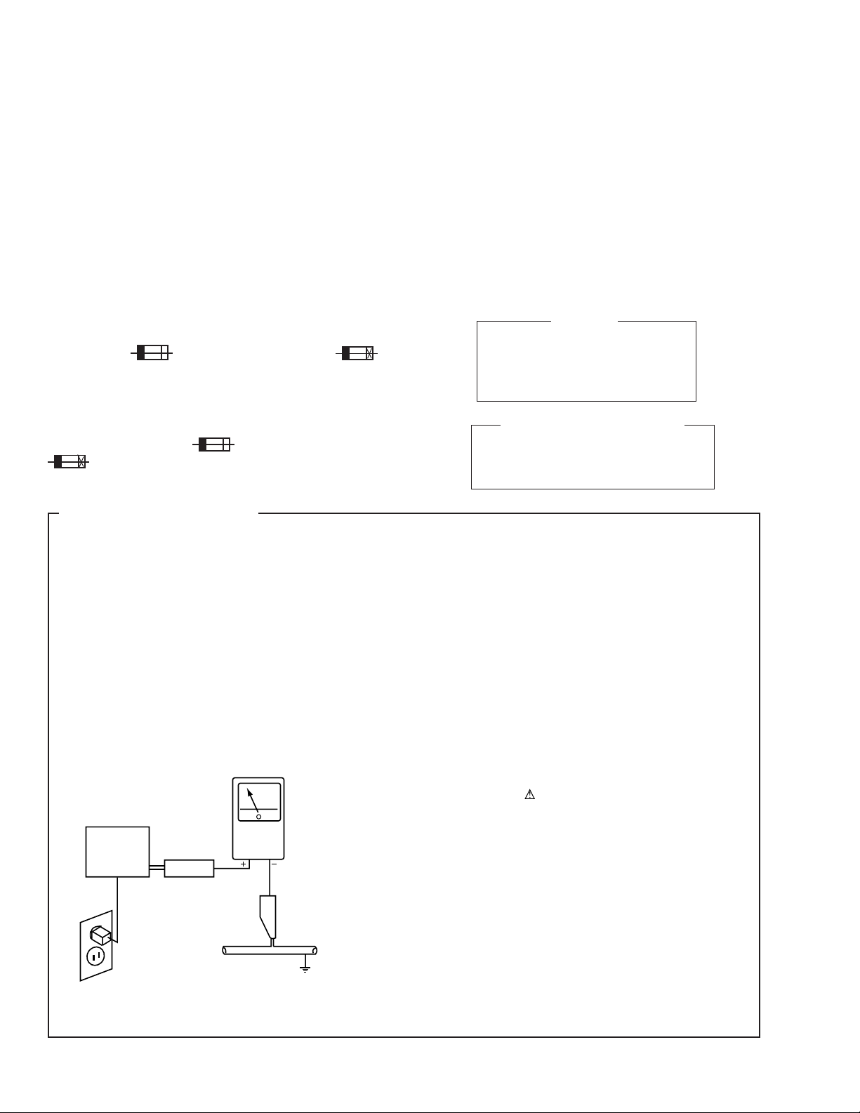
1. SAFETY PRECAUTIONS
The following check should be performed for the
continued protection of the customer and service
technician.
LEAKAGE CURRENT CHECK
Measure leakage current to a known earth ground (water
pipe, conduit, etc.) by connecting a leakage current tester
such as Simpson Model 229-2 or equivalent between the
earth ground and all exposed metal parts of the appliance
(input/output terminals, screwheads, metal overlays, control
shaft, etc.). Plug the AC line cord of the appliance directly
into a 120V AC 60Hz outlet and turn the AC power switch
on. Any current measured must not exceed 0.5mA.
Reading should
not be above
0.5mA
Earth
ground
Device
under
test
Also test with
plug reversed
(Using AC adapter
plug as required)
Leakage
current
tester
Test all
exposed metal
surfaces
IMPORTANT
THIS PIONEER APPARATUS CONTAINS
LASER OF CLASS 1.
SERVICING OPERATION OF THE APPARATUS
SHOULD BE DONE BY A SPECIALLY
INSTRUCTED PERSON.
LASER DIODE CHARACTERISTICS
FOR DVD : MAXIMUM OUTPUT POWER : 5 mW
FOR CD : MAXIMUM OUTPUT POWER : 5mW
WAVELENGTH : 655 nm
WAVELENGTH : 785 nm
ANY MEASUREMENTS NOT WITHIN THE LIMITS
OUTLINED ABOVE ARE INDICATIVE OF A POTENTIAL
SHOCK HAZARD AND MUST BE CORRECTED BEFORE
RETURNING THE APPLIANCE TO THE CUSTOMER.
2. PRODUCT SAFETY NOTICE
Many electrical and mechanical parts in the appliance
have special safety related characteristics. These are
often not evident from visual inspection nor the protection
afforded by them necessarily can be obtained by using
replacement components rated for voltage, wattage, etc.
Replacement parts which have these special safety
characteristics are identified in this Service Manual.
Electrical components having such features are identified
by marking with a
in this Service Manual.
The use of a substitute replacement component which does
not have the same safety characteristics as the PIONEER
recommended replacement one, shown in the parts list in
this Service Manual, may create shock, fire, or other hazards.
Product Safety is continuously under review and new
instructions are issued from time to time. For the latest
information, always consult the current PIONEER Service
Manual. A subscription to, or additional copies of, PIONEER
Service Manual may be obtained at a nominal charge from
PIONEER.
on the schematics and on the parts list
AC Leakage Test
2
Page 3
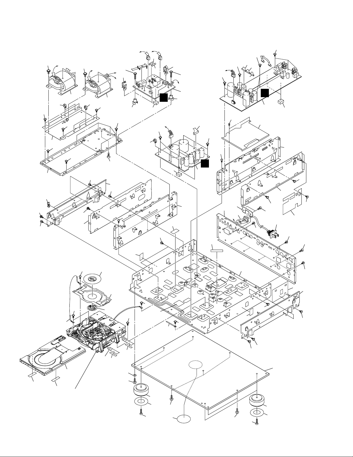
2. EXPLODED VIEWS AND PARTS LIST
NOTES:• Parts marked by "NSP" are generally unavailable because they are not in our Master Spare Parts List.
The mark found on some component parts indicates the importance of the safety factor of the part.
•
Therefore, when replacing, be sure to use parts of identical designation.
Screws adjacent to mark on the product are used for disassembly.
•
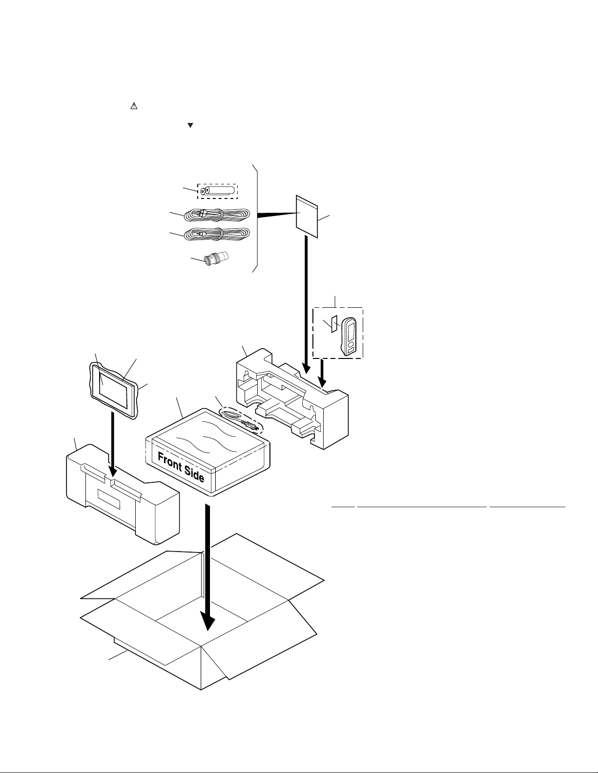
2.1 PACKING
7
DV-AX10
13
4
12
5
2
×3
9
10
14
3
8
12
16
L
1
÷ PACKING PARTS LIST
15
R
Mark No. Description Part No.
1 Mirror Mat Bag VHL1004
2 BNC to RCA/phono adapter VKX1004
NSP 3 Warranty Card ARY7045
4 Audio Cord (L= 1.5m) VDE1023
5 Video Cord (L= 1.5m) VDE1024
6 • • • • •
NSP 7 Dry Cell Battery (R6P, AA) VEM-013B
8 Operating Instructions VRB1223
(English/French)
9 Remote Control Unit VXX2631
(CU-DV041)
10 Battery Cover VNK4422
11 • • • • •
NSP 12 Polyethylene Bag Z21-038
(0.03 x 230 x 340)
13 Front Pad AHA9016
14 Rear Pad AHA9017
15 Packing Case VHG1811
16 Packing Sheet AHG7008
3
Page 4
DV-AX10
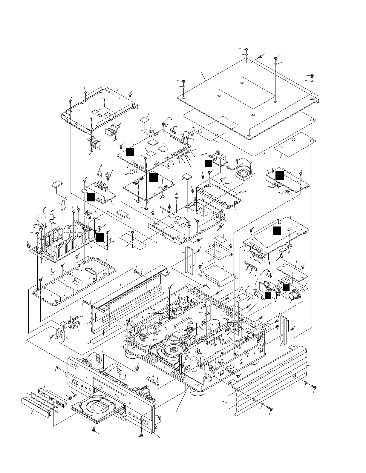
2.2 EXTERIOR SECTION(1/2)
39
32
53
39
40
39
65
42
N
54
D
M
63
62
39
S
40
39
L
C
S
7
39
39
35
A
40
72
22
38
S
67
36
24
37
70
14
39
A
12
13
40
39
E
O
33
B
M
50
4
32
52
39
51
76
23
20
39
1
65
22
39
15
10
73
9
10
72
30
39
50
41
17
D
39
L
N
P
Q
39
46
S
J
I
48
H
K
2
80
34
34
19
66
40
47
39
39
40
39
L
K
31
58
68
79
T
39
71
31
18
57
66
40
57
78
39
43
16
41
39
T
E
R
75
49
O
30
F
40
73
S
C
64
10
73
10
73
11
43
39
77
56
69
8
M
P
Q
39
55
3
G
H
I
J
U
F
G
74
J
39
57
R
61
32
V
44
6
59
39
60
K
5
83
82
64
45
19
28
4
29
27
39
26
25
40
39
64
E
F
G
Refer to
"2.3 EXTERIOR SECTION(2/2)".
Refer to
"2.4 FRONT PANEL SECTION".
B
67
T
U
V
39
73
22
21
73
22
Page 5

DV-AX10
÷ EXTERIOR SECTION(1/2) PARTS LIST
Mark No. Description Part No. Mark No. Description Part No.
1 DVDM Assy VWS1475
2 DSPB Assy VWG2159
3 MAUD Assy VWV1735
4 DOUT Assy VWG2162
NSP 5 BLOUT Assy VWV1743
NSP 6 BLSW Assy VWG2170
7 SYPS Assy VWR1324
8 VOUT Assy VWV1760
9 Top Plate AAH7039
10 SH Screw PBA1049
NSP 11 Inside Plate VNA2107
12 Main Shield T VNE2226
13 AV1 Heat Sink VNH1052
14 FTS Heat Sink VNH1053
15 Locking Card Spacer ONK1035
16 Trans. Shield VNE2138
17 Main Shield B VNE2227
18 Shield Sheet M2 VEC2140
19 Rear Mole AAH7044
20 Side Alum. L AAH7040
21 Side Alum. R AAH7041
22 Screw (4 x 20) ABA7006
23 Subchassis T VNE2180
24 PW-SW-Holder VNE2204
25 P Screw VBA1057
26 Door Spring VBH1305
27 Door Holder VNK4605
28 Door Packing VEC2045
29 Tray Panel VNK4398
30 Gap Pad VEC1997
41 Cord Clamper RNH-184
42 Housing Assy (3P) VKP2241
NSP 43 Spacer PNM1135
44 Housing Assy (4 + 4/10P) VKP2240
45 Screw PMA30P060FCU
46 Housing Assy Assy (14P) VKP2231
47 Housing Assy Assy (13P) VKP2233
48 Housing Assy Assy (15P) VKP2236
49 Housing Assy Assy (15P) VKP2229
50 Rubber Spacer REB1218
51 Gaurd Sheet VEC2146
52 Rivet(Plastic) VEC-213
53 Housing Assy Assy (8P) VKP2238
NSP 54 Shield Tube VDM1003
55 Flexible Cable (16P) VDA1810
56 Flexible Cable (28P) VDA1811
57 Screw BBZ30P080FCC
58 Shield Plate H AMR7309
59 SHLD Assy VWR1321
60 PCB Shield A VEC2126
NSP 61 Spacer VEC1532
62 Housing Assy Assy (10P) VKP2237
NSP 63 Shield Tube VDM1004
64 Screw IBZ30P080FCC
65 Radiation Seat VEB1314
NSP 66 Space AED7043
67 Shield Sheet A VEC2127
68 Shield Sheet B VEC2128
69 Shield Sheet C VEC2144
70 Shield Sheet D VEC2145
NSP 32 Holder (B) VEC1381
31 Board Holder DEC1231
33 Spacing Clip VEC2133
NSP 34 Card Spacer QEC1012
NSP 35 Spacer DEC1316
36 Switch PSG1011
37 Screw PMA30P060FCU
38 FLEX SW Wire VDX1008
39 Screw ABA1011
40 Screw IBP30P090FCC
71 Fuse Caution Label VRW1770
72 Washer WH40FUC
73 Washer WA40F080M050
NSP 74 Label VRW1629
NSP 75 ID Label VRW1825
76 Shield Sheet E VEC2156
77 DC Fan Motor VXM1072
78 Screw BBZ30P150FMC
NSP 79 FANB Assy VRW1325
80 Sheet VEX1022
81 Screw BBZ30P060FCC
82 Screw BMZ26P050FCU
83 Cap VEC2076
5
Page 6
DV-AX10
2.3 EXTERIOR SECTION(2/2)
51
48
42
42
63
28
27
A
30
42
48
51
B
6
48
48
14
42
30
42
50
E
33
D
7
42
35
16
42
47
34
11
42
I
1
42
48
61
13
42
15
42
55
10
42
62
B
A
30
49
8
47
42
18
48
E
31
58
68
C
42
U
33
50
C
3
34
D
36
29
52
42
H
2
12
53
9
42
66
64
42
65
42
29
54
46
45
26
29
5
Refer to
"2.5 LOADING MECHANISM ASSY".
23
43
24
25
46
44
44
37
38
32
42
39
20
22
40
41
38
67
42
38
19
32
39
42
48
42
20
22
21
56
42
17
42
6
Page 7

÷ EXTERIOR SECTION(2/2) PARTS LIST
DV-AX10
Mark No. Description Part No.
1 AUDIO Assy VWV1735
2 MAPS Assy VWR1322
3 LSFB Assy VWR1320
4 • • • • •
NSP 5 Loading Mechanism Assy VWT1158
6 Main Power Transformer VTT1161
7 Audio Power Transformer VTT1162
8 Fuse (FU1 : 1A) VEK1014
9 Fuse (FU2 : 2A) VEK1019
10 AC Power Cord VDG1046
11 Shield Sheet P VEC2060
12 Side Wall L2 VNE2177
13 Side Wall R2 VNE2178
14 Side Suport A VNE2183
15 Side Suport B2 VNE2229
16 Side Frame A VNE2181
17 Side Frame B VNE2182
18 Rear Panel VNA2038
NSP 19 Under Base VNA2040
20 Insulator ANL7013
21 Buttom Plate C VNA2171
22 Cushion AEC7224
23 Clamper Plate VNE2114
24 Bridge VNE2113
25 Clamper VNL1738
26 Tray VNK4243
27 Trans. Plate VNE2203
28 Sub Chassis B VNE2179
29 Sheet VEX1022
NSP 30 Holder (B) VEC1381
Mark No. Description Part No.
36 Rubber Spacer REB1218
37 Washer WH30FUC
38 Schew IBZ30P120FCC
39 Schew BBZ30P200FMC
NSP 40 Base Cushion VEC1107
41 Cord Clamper RNH-184
42 Schew ABA1011
43 Flexible Cable (12P) VDA1813
44 Spacer VEB1319
NSP 45 Earth Lead Wire DE007VF0
46 Schew IBZ30P080FCC
47 Schew BBZ30P060FCC
48 Schew IBP30P090FCC
NSP 49 Rubber Spacer PEB1194
50 Schew IBZ30P180FCC
51 Schew VBA1056
52 Housing Assy (8P) VKP2239
NSP 53 Tape (K) REH1011
54 Schew BPZ26P080FZK
55 Side Shield L VEC2124
56 Side Shield R VEC2125
57 • • • • •
58 Power Cord Spacer ANG1153
59 • • • • •
60 • • • • •
NSP 61 Rubber Spacer REB1187
62 Schew BBZ30P080FCC
63 Side Clamp DEC2007
64 Housing Assy (15P) VKP2230
65 Housing Assy (14P) VKP2232
31 Rivet (Plastic) VEC-213
32 Tape (G) REH1010
NSP 33 Wire Clip DEC1450
NSP 34 PCB Mold AMR1525
NSP 35 PCB Holder PNW2029
66 Housing Assy (13P) VKP2234
67 UL Caution Card AAX-313
68 UL Tubing VEC1651
7
Page 8
DV-AX10
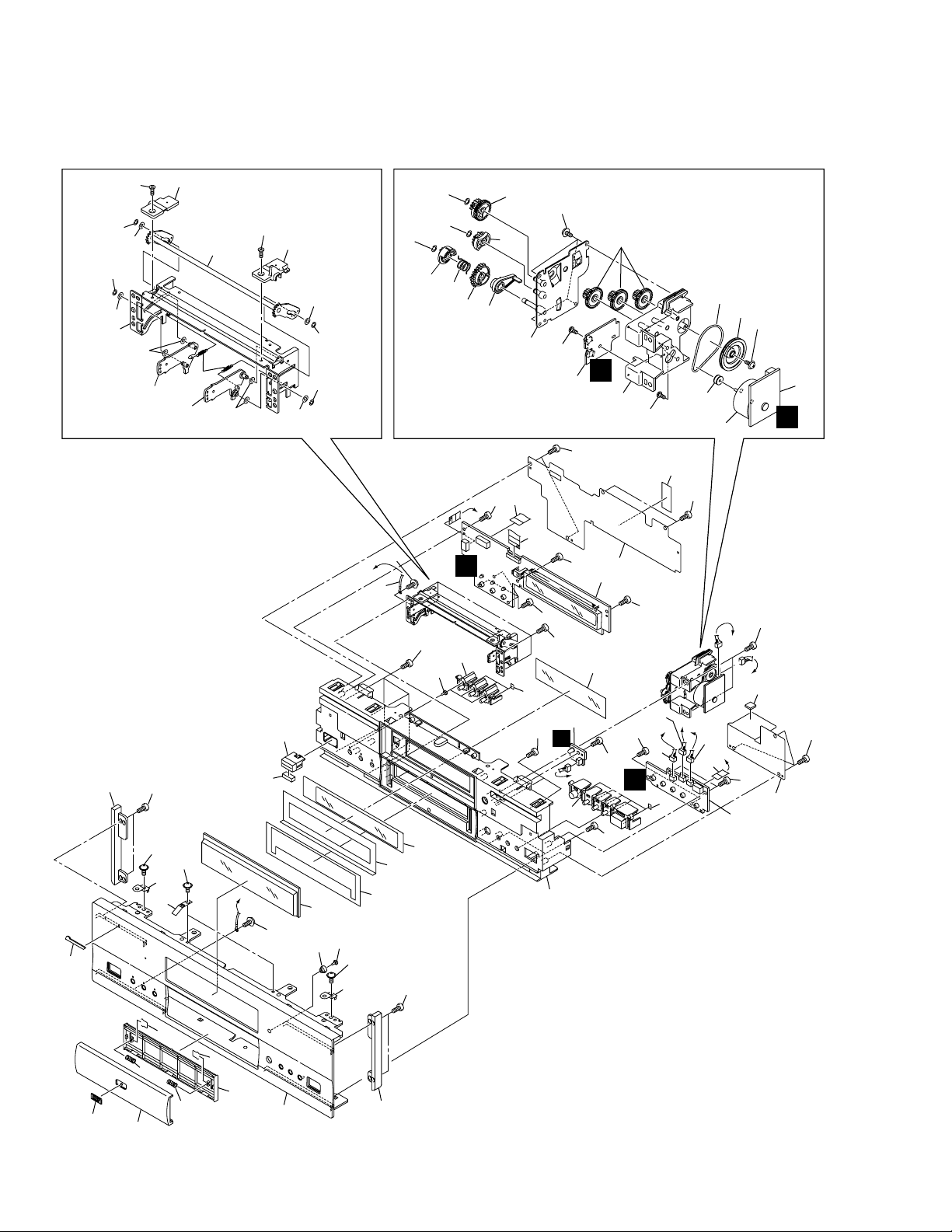
2.4 FRONT PANEL SECTION
12
13
56
55
34
56
54
55
55
35
57
71
16
15
32
36
65
37
33
55
53
21
53
57
22
40
58
53
41
42
N
26
25
54
32
55
56
56
55
65
E
64
23
70
E
19
65
17
20
18
65
15
43
D
62
39
38
67
44
27
66
58
62
24
51
51
62
R
29
45
47
48
51
Q
4
46
52
62
62
31
1
62
28
3
A
62
61
62
O
58
60
C
27
69
49
50
62
B
C
B
A
59
D
63
62
2
5
P
62
68
62
30
10
8
6
7
10
8
9
11
14
8
Page 9

÷ FRONT PANEL SECTION PARTS LIST
DV-AX10
Mark No. Description Part No.
1 FLKB Assy VWG2164
2 PLSB Assy VWG2166
NSP 3 LEDB Assy VWG2167
NSP 4 DRSB Assy VWG2168
NSP 5 DRMB Assy VWG2169
6 DVD Plate VAM1096
7 Door Aluminum VAH1307
8 Earth Spring VBH1310
9 Door Base VNK4396
10 Clip (SUS) VBM1003
11 Front Aluminum VAH1306
12 Name plate G PAN1377
13 Side Panel L AAH7042
14 Side Panel R AAH7043
15 Top Stay VNE2139
16 Earth Plate VBK1075
17 DVD Ring VAK1008
18 DISP Lens PNW2113
19 FL Lens C VEC2034
20 Shield Cushion VEC2036
21 Inner Aluminum VAH1311
22 FL Lens S VEC2085
23 Power Button VNK4888
24 Panel Base VNK4390
25 LED Lens VNK4400
26 Function Key VNK4394
27 Tape PNM1017
28 FL Filter VEC1965
29 Main Key VNK4392
30 Shield Sheet S VEC2039
Mark No. Description Part No.
36 Drive Arm R Assy VXA2363
37 Door Spring B VBH1300
38 Drive Gear A VNL1792
39 Drive Gear B VNL1793
40 Drive Gear D VNL1795
41 Door Spring A VBH1299
42 Drive Gear C VNL1794
43 Switch Arm VNL1797
44 Gear Base Assy VXA2365
45 Gear (C) VNL1047
46 Moter Holder VNL1796
47 Belt (Rubber) PEB1288
48 Gear Pulley VNL1733
49 Moter Pulley PNW1634
50 DC Moter 0.75W (DISC DOOR) PXM1010
51 Screw Z39-019
52 Screw BMZ26P040FMC
53 Washer WT31D054D050
54 Screw CBZ26P060FMC
55 Washer WA32D080D025
56 Washer WT26D047D050
57 Screw ABA7017
58 Screw BBZ30P080FZK
59 Connector Assy PG03KK-E07
60 Connector Assy PG03KK2E07
61 Connector Assy PG03KK4E07
62 Screw BPZ30P080FCC
63 Flexible Cable (8P) VDA1814
NSP 64 Earth Lead Wire DE005VF0
65 Screw ABA1011
31 Shield Sheet L VEC2038
32 Drive Shaft Holder VNL1791
33 Drive Arm Assy VXA2364
34 Door Support VNE2140
35 Drive Arm L Assy VXA2362
66 Flexible Cable (19P) VDA1809
67 Flexible Cable (13P) VDA1812
68 Spacer VEC-244
NSP 69 Tape (K) REH1011
70 Block ANL7015
71 Screw IBP30P090FCC
9
Page 10

DV-AX10
2.5 LOADING MECHANISM ASSY
• Top View • Bottom View
9
20
Refer to
"2.4 TRAVERSE MECHANISM ASSY-S".
23
14
1
19
23
25
22
23
21
24
18
17
2
7
8
16
B
9
10
11
13
15
3
A
12
4
5
6
LOADING MECHANISM ASSY PARTS LIST
Mark No. Description Part No. Mark No. Description Part No.
NSP 2 LOSB Assy VWG1885
1 Traverse Mechanism Assy-S VXX2653
NSP 3 LOMB Assy VWG1886
4 Drive Gear VNL1735
5 Lock Plate VNL1820
6 Loading Base VNL1844
7 Belt VEB1260
8 Gear Pulley VNL1733
9 Screw DBA1006
10 Loading Gear VNL1734
11 Loading Motor Assy VXX2505
12 DC Motor / 0.3W (LOADING) PXM1027
13 Motor Pulley PNW1634
14 Drive Cam VNL1736
15 Connector Assy VKP2198
(LOMB CN401 ↔ LOSB CN303)
NSP 23 Stop Cushion VEC1605
NSP 25 Earth Lead Wire DE010VF0
16 Screw VBA1055
17 Screw Z39-019
18 Flexible Cable (08P) VDA1698
(LOSB CN302 ↔ SMEB CN202)
19 Float Base VNL1867
20 Floating Rubber VEB1286
21 Flexible Cable (24P) VDA1804
(Pickup Assy ↔ DVDM CN120)
22 Screw PBZ26P050FCC
24 Tray Stabilizer VNE2210
10
Page 11

2.6 TRAVERSE MECHANISM ASSY-S
• Top View
DV-AX10
37
37
17
31
24
30
16
35
33
28
5
22
33
21
23
10
15
2
D
10
10
14
7
7
34
19
8
6
20
12
9
37
4
10
13
37
18
32
1
18
26
11
25
27
7
29
36
3
C
TRAVERSE MECHANISM ASSY-S PARTS LIST
Mark No. Description Part No. Mark No. Description Part No.
NSP 1 SMEB Assy VWG2048
NSP 2 FGSB Assy VWG2009
NSP 3 Motor (CARRIAGE) VXM1079
NSP 4 Motor (SPINDLE) VXM1078
NSP 5 Pickup Assy VWY1055
6 Table Sheet DEC2040
7 Screw VBA1058
8 Centering Spring VBH1278
9 Hook Spring VBH1317
10 Skew Spring VBH1303
11 Gear Spring VBH1308
NSP 12 Reflected Sheet VEC1959
13 Guide Bar VLL1504
14 Sub-guide Bar VLL1505
15 Hold Spring VNC1017
NSP 16 Magnet Holder VNE2070
NSP 17 Motor Base VNE2154
NSP 18 Cover VNE2155
19 Centering Ring VNL1746
NSP 20 Disc Table VNL1747
NSP 30 Magnet VYM1024
21 Hook VNL1770
22 FFC Holder VNL1802
23 Mechanism Base VNL1806
24 FG Holder VNL1807
25 Gear A VNL1808
26 Gear B VNL1809
27 Gear C VNL1810
28 Slider VNL1811
29 Gear D VNL1814
31 Screw JFZ17P025FZK
32 Screw JGZ17P028FMC
33 Screw VBA1051
34 Magnet Holder Assy VXX2507
35 Spindle Motor Assy VXX2649
36 Carriage Motor Assy VXX2650
37 Screw PBA1069
11
Page 12
DV-AX10
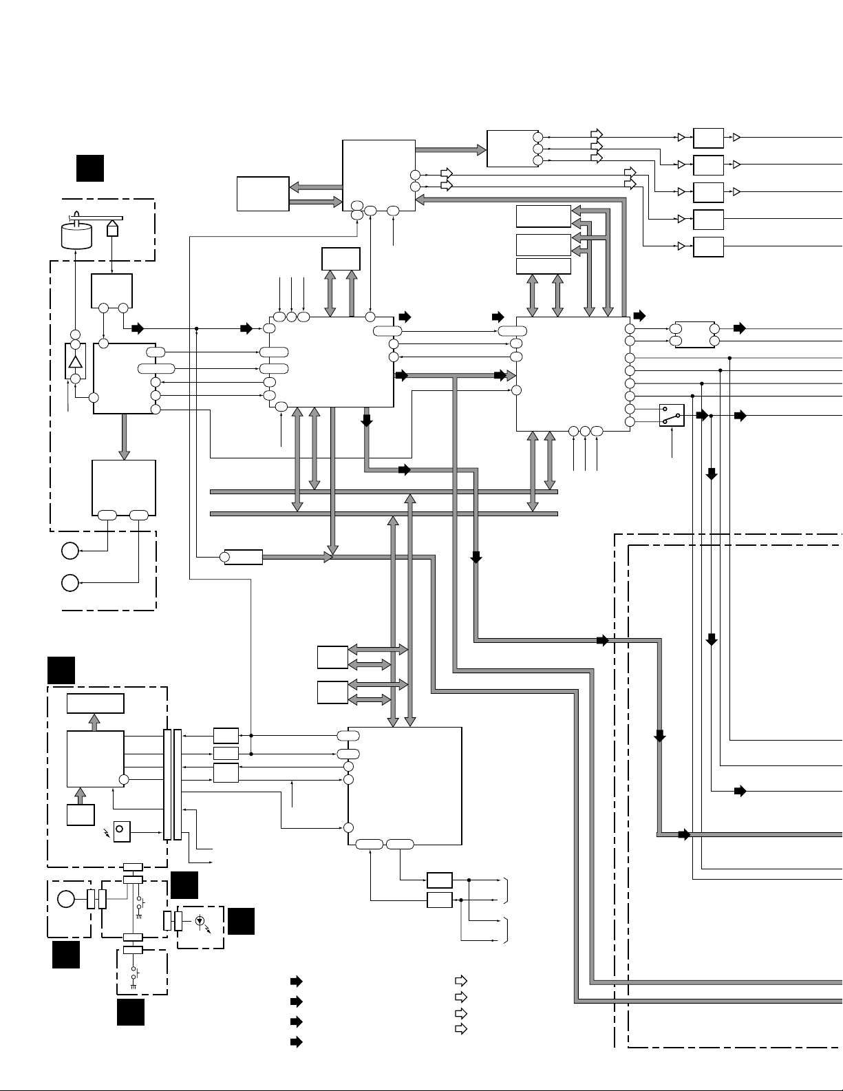
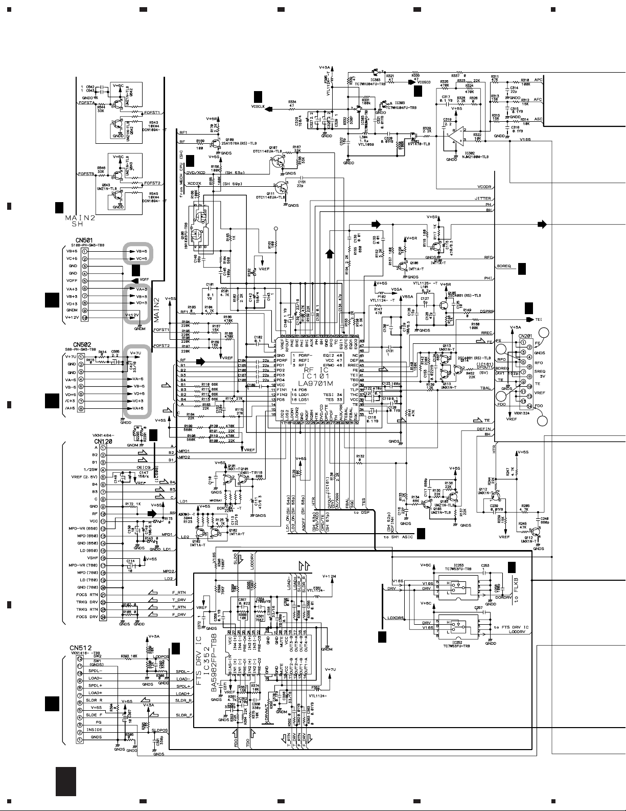
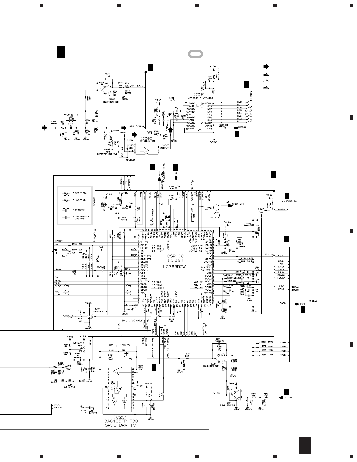
3. BLOCK DIAGRAM AND SCHEMATIC DIAGRAM
3.1 BLOCK DIAGRAM
E
Spindle
Motor
LA9701M
12
13
25
45
SPDO
IC251
BA6195FP
SPDL DRIVE
M
CARRIAGE
M
LOADING
DVDM ASSY
Pickup
IC101
RF IC
46
54
RFO
EFMO
39
LC78652W
Servo DSP
BA5982FP
FTS Drive IC
15,16 17,18
IC201
IC
Servo Control
IC352
3,5,4
10
55
19
SBCK
FGPL
DOUT
HY58163210TQ-10F
ROMXA,LRSY,
ROMCK
C2F,SFSY,
SBSY,PW
ADDRESS
DATA
IC301
ADC08351CIMTC
8 bit A/D
VIN
17
IC1002
16M SGRAM
IC702
KM48V8104CS-6
64M DRAM
VCOCLK
181
170
AIN
112-114
116-1192,11,18,12
EXCK
120
162
165
RD1-RD8
MQA0-MQA9
MQD0-MQD31
16M
27/33M
107
5
PE5220A
DVD DECODER
BY Chip ES2
XRESET
D0-D7
A0-A16
SSO,SSCK
DD0-DD7
IC701
ADD0-ADD7
RD1-RD8
IC1001
PM0024AF
VIDEO
ENCODER
207
204
206
DA0-DA12
(D)
Video Data
(C)
C
53
(Y)
Y
VQE3
SGL
10
ASDAT0-ASDAT7
50
CPN0-CPN7,DACK,XHS,XVS
205
111-109
54
56
M5M4V18165DTP-6S
XCSVE
(C) (C)
CDDATA,CDBCLK,CDLRCK
(D)
IC1003
CXD2307R
IC803
IC804
M5M4V18165DTP-6S
IC802
M2V64S40BTP-8L
BCLK
SREQ
BD0-BD7
48,45,44
(D)
Cr
58
Cb
54
Y
D/A
50
16M EDO
DRAM
16M EDO
DRAM
64M SDRAM
MA0-MA11
160
IC801
162
M65774FP
MPEG2 DECODER
AV-1
46
CDDATA
(SPDIF)
A1-A9
D0-D15
(Cr)
(Cb)
MD0-MD15
DOUT1(STREAM)
64
36/16M
(Y)
NMA0-NMA9
NMD0-NMD15
DOUT0(PCM)
LRCLK
DOCLK
106
55
27M
HXRST
(C)
(Y)
(AC)
HLRCK
HBCK
AO1
AO2
AO0
AOD
DOUT1
DOUT0
IC901
IC915,IC916
TC7SET08FU
Converter
1,2
1,2
1
2
6
AOSEL0
CPN0-CPN7,DACK,XHS,XVS
73
74
81
80
70
AO1
69
AO2
71
AO0
68
AOD
TC7WH157FU
Video Filter
F1311
F1361
F1411
F1461
F1511
F1561
F1201
F1251
3 → 5
4
4
(C)
5
(C)(C)
(AC)
AC3
PCM
(C)
N
FLKB ASSY
V101
FL Tube
IC101
PE5047A
FL Control
KEY
SW
REMOTE
SENSOR
CN351
M
DOOR
P
DRMB
ASSY
12
CN301
CN302
XRESET
27
CN101
Q
CN101
9
11
CN303
CN304
CN341
DRSB
ASSY
IC501
TC7WH126FU
IC611
TC74VHCT541AFT
3 → 5
Converter
CN503
O
IC611
IC501
IC612
5 → 3
9
Converter
IC612
TC74VHCT541AFT
11
SEL IR
IR
PLSB ASSY
CN331
TC55V1001AF8
WORK 1M
FLASH MEMORY
LEDB
R
ASSY
IC604
SRAM
IC603
VYW1648
PGM 16M
SSO,LT1
99,78
SSCK,SSI
HXRST
DORPOS
103,98
97
82
86
XRDY,DORPOS
HXRST
: RF SIGNAL ROUTE
(D)
: AUDIO DATA ROUTE (DVD)
(C)
: AUDIO DATA ROUTE (CD)
(AC)
: AC-3, DTS SIGNAL ROUTE
A0-A16
D0-D7
A1-A20
D0-D15
IC601
PD3410A
SH1
BASE ASIC
101,117 102,118
TXD,DTR
RXD,CTS
TC74VHC541FT
3,2
16,15
IC612
3 → 5
Converter
5 → 3
Converter
(Cr)
(Cb)
17
TXD5
4
RXD5
TXD5
RXD5
(Y)
: Y SIGNAL ROUTE
(C)
: C SIGNAL ROUTE
: Cr SIGNAL ROUTE
: Cb SIGNAL ROUTE
ASDAT0-ASDAT7
For PEC DIF
attestation
For Down load
(D)
CN510
CN513
(D)
(C)
(D)
CN103
CN105
Page 13
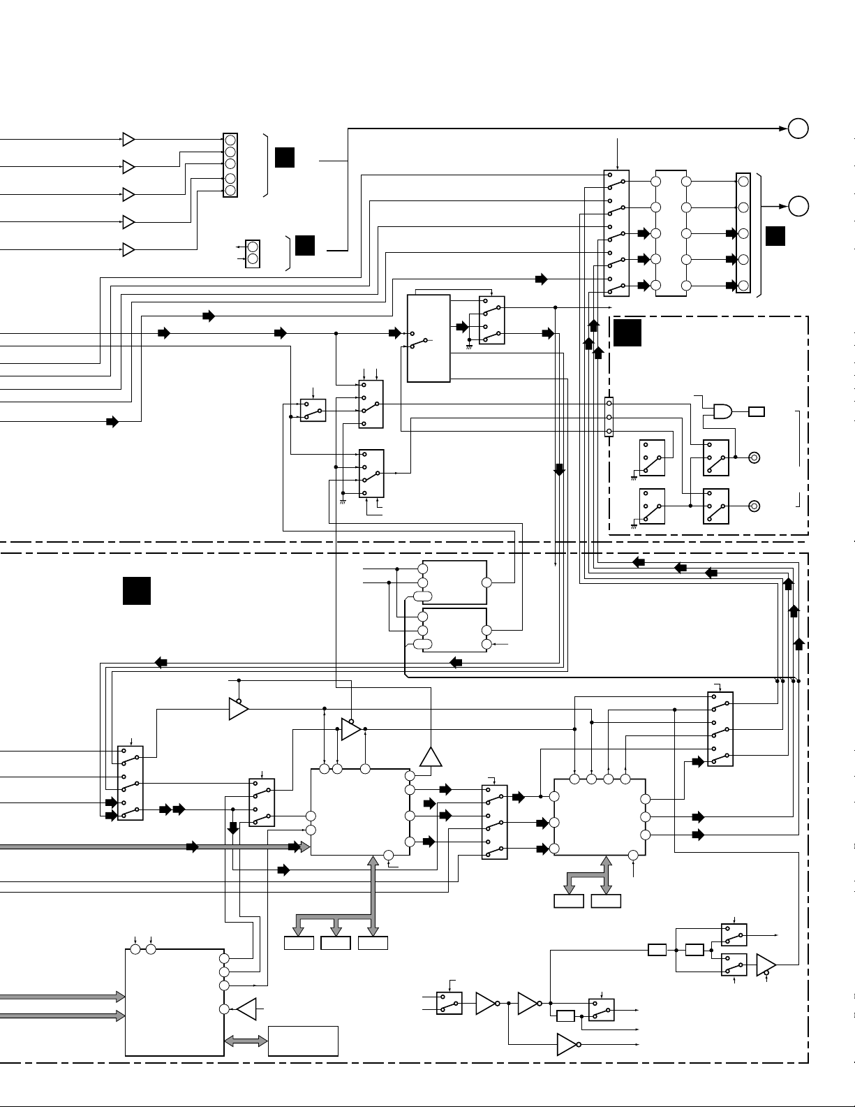
DV-AX10
57
IC1631-2/2
31
IC1631-1/2
57
IC1691-2/2
31
IC1201-1/2
57
IC12011-2/2
(C)
(AC)
(C)
20
22
24
10
8
CN506
SEL IR
TC7WH157FU
CR/R
CB/B
Y/G
C
Y
CN507
3
2
IC911
M
CN601
SEL IR
IRIR
(AC)
M
CN602
AC3
DO1SEL0
6
1
2
PCM
3
5
4
5
1
TC74VHC153FT
12
11
13
1
14
(AC)
DO1SEL1
DO1SEL2
2
14
7
IC907
9
TC74VHC153FT
2
DO2SEL1
DO2SEL2
34
3
4
IC909
DI_ERRS
CKOUT
DATAO
BCK
LRCK
DIN
IC905
TC74VHC157FT
2
13
3
(AC)
14
16
13
14
15
PDIFL
PDIFR
4
12
DIRCLK
DIRDAT
DIRBCK
DIRLCK
IC902
TC74VHC157FT
IC904
TC7WH157FU
IC904-2
IC902-13
HBCK
IC902-6
AO1
IC902-10
AO2
(C)
IC902-3
AO0D
(AC)
(AC)
HLRCK
(D)
(C)
(D)
(D)
4
7
9
AOSEL1
DIRCLK
L
CN801
CN508
IC906
TC74VHCT541AFT
3 → 5
Converter
5
12
(D)
7
(D)
9
4
(C)
(D)
LRCK
15
5
BCK
6
14
ADATA1
3
17
ADATA2
2
18
ADATA0
4
16
DOUT ASSY
XTOFF
7
IC831
TC74VHC153FT
(C)
IC841
5
6
(D)
(D)
CN505
(D)
3
9
7
13
15
11
JA921
JA911
JA931
A
B
G
CN602
OPT
2 COAX
DIGITAL
OUT/PDIF
1 COAX
PCM
F
AV1/XDIR
9
7
(C)
(AC)
TC74VHC157FT
4
IC161
MCLK(768fs)
14
80
MCKI
SD0-SD7
WAD1-WAD-7
SACD DECODER
DSPB ASSY
(AC)
XEXCKON
(LRCK)
(C)
(AC)
(D) (D)
VCOCLK
WCK
IC801
CXD2751Q
5
IC158-2/2
TC7WH125FU
IC152
TC74VHC157FT
(C)
BCKD
46
BCKA
DSDR
48
DSAR
DSDL
47
DSAL
13
7
3
SACDSL
5
6
2
3
IC158-1/2
TC7WH125FU
(BCK)
7
4 DATA
10
SDI1
11
SDI0
(C)
IC921
PDK038A
DTS ROM
XRESET
KM48V8104CS-6
TC55V8128BJ-12
IC802
64M DRAM
1
2
15
12
SCKR
FST/FSR
IC101
XCD56362PV100
DSP1
DVD-A DOLBY,
IC911
1M SRAM
128FS
48/X44
6
14
AD0(DAX)
SCKT
DTS
44
IC901
KM616V1002CT-12
1M SRAM
HAD0
27
4
5
6
RESET2
36/33M
DIRCLK
5
IC502
CS8404A-CS
4
DIT
8,6,7
5
IC501
CS8404A-CS
4
DIT
8,6,7
IC104
TC7SET08FU
3 → 5
Converter
AV1/XDSP1
SDO0
SDO0 2
(C)
(D)
DATA 3
SDO0 5
SDO1
(D)
SDO2
SDO2 11
(D)
IC164
TC7WH157FU
PDIFR
20
PDIFL
20
16
(AC)
AO2 6
AO1 10
IC162
TC74VHC157FT
AV1/XDIR2
DITRST
4 SDI02
(D)
7 SDI12
4 SDI22
10
(C)
11
(D)
12
(D)
TC55V8128BJ-12
1M SRAM
MCLK
DIRCLK
FSR
SCKR
13
15
SDI0
IC201
XCD56362PV100
DSP2
SDI1
Water Mark
Delay Adjust
SDI2
IC931
IC951
KM616V1002CT-12
1M SRAM
1/2
FST
SCKT
12
14
4
5
6
44
RESET2
IC151
ACICKSL
TC7WH157FU
ACI
DSP1
HCKT
DSP1&DSP2
SACD
(D)
SDO0
SDO1
SDO2
1/3
(D)
(D)(C)
DCMD2CSL
BCK 6
LRCK 10
2
3
(C)
(D)
IC162
TC74VHC157FT
(D)
(D)
1/2
IC554
TC7WH157FU
7 DSPBCK
9 DSPLRCK
4 DSPDO0
IC553
DITCKSLSEL96K
TC7WH157FU
128FS
XSCKT_IN
(D)(C)
(D)
(D)
DIT
13
Page 14

DV-AX10
A
B
CN601
CR/R
CB/B
Y/G
C
Y
20
22
24
10
8
(Cr)
(C)
(Y)
IC608-IC610
TC7W53FU
(Cb)
(Y)
IC606-2/2
5
6
6
7
6
7
IC610
IC609
7
6
7
1
1
IC608
IC607-1/2
2
3
IC607-2/2
6
5
IC606-1/2
1
(Cr)
1
(Cb)
7
2
3
1
JA653
(Y)
Y
CB
CR
COMPONENT
VIDEO OUT
VOUT ASSY
M
CN602
SEL IR
CONTROL
IC604-2/2
6
5
IC604-1/2
2
3
7
1
(C)
(C)
IC602-1/2
3
1
2
(Y)
IC602-IC607
TK15420M
IC603-1/2
2
3
IC603-2/2
6
5
IC605-1/2
2
3
IC605-2/2
6
5
3
2
IR
JA660
JA661
(C)
1
(C)
7
(Y) (Y)
1
(Y) (Y)
7
IN
OUT
(C)
JA651
JA652
1
2
VIDEO OUT
1
S2-VIDEO OUT
2
14
(D)
: AUDIO DATA ROUTE (DVD)
(C)
: AUDIO DATA ROUTE (CD)
: AUDIO SIGNAL ROUTE
: VIDEO SIGNAL ROUTE
(Y)
: Y SIGNAL ROUTE
(C)
: C SIGNAL ROUTE
(Cr)
: Cr SIGNAL ROUTE
(Cb)
: Cb SIGNAL ROUTE
Page 15

DV-AX10
CN602
ADATA2
ADATA1
ADATA0
LRCK
BCK
1
3
5
7
9
CN605
TC74VHCT541AFT
(D)
2
(D)
4
6
8
(C) (D)
5
ADATA0
CN101
ADATA0
IC603
DATA2I
18
DATA1T
16
MAUD ASSY
G
IC131
PD0236AM
11
Hi-Bit
I
AUDIO ASSY
IC661
PD0236AM
814 3
Hi-Bit
IC671
PD0236AM
814 3
Hi-Bit
IC681
SM5847AF
Digital Filter
814 3
20
IC681
SM5847AF
Digital Filter
20
2
IC691
SM5847AF
Digital Filter
20
2
DOL
DOR
2
IC301,IC321,IC351,IC371
PCM1704U
DAC
IC701
DOL
DOR
IC711
IC721
DOL
DOR
IC731
IC701,IC711,IC721,IC731
PCM1704U
DAC
IC301
141
IC321
141
IC351
141
IC371
141
AUDIO OUT
1
JA302
JA352
1
CENTER
SUB WOOFER
L
SURROUND
R
CN301 CN901
L
FRONT
R
4
3
2
1
10
JA901
1
2
9
JA951
L
AUDIO
OUT
R
J
141
141
141
141
IC342-1/2
2
3
IC392-1/2
2
3
BLOUT
ASSY
15
Page 16
1
23
4
DV-AX10
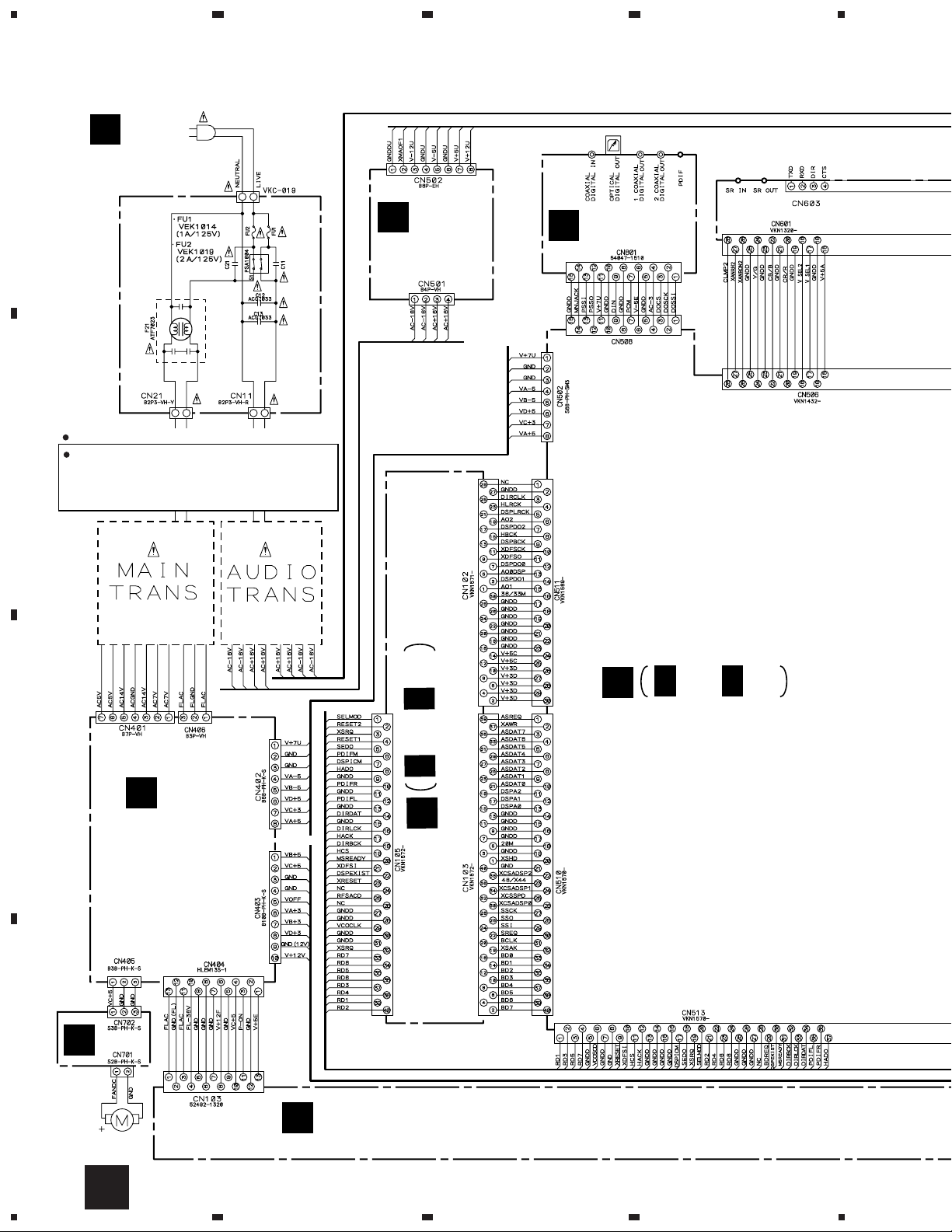
3.2 OVERALL CONNECTION DIAGRAM, LOMB, LOSB, SMEB, FGSB and LSFB ASSYS
AC POWER CORD
AC120V
U
A
LSFB ASSY
60Hz
(VWR1320)
NOTE FOR FUSE REPLACEMENT
B
CAUTION :
AGAINST RISK OF FIRE,REPLACE
WITH SAME TYPE AND RATINGS
ONLY.
FOR CONTINUED PROTECTION
VDG1046
ACE7014
ACE7014
H
MAPS ASSY
(VWR1322)
DOUT ASSY
L
(VWG2162)
VKP2229
FOR RS-232C
VTT1161
VTT1162
F 2/2
E
E 1/5- E 5/5
DVDM ASSY
(VWS1475)
C
F 1/2-
S
SYPS ASSY
(VWR1324)
FANB ASSY
(VWR1325)
F
DSPB ASSY (VWG2159)
T
D
16
FLKB ASSY
FAN MOTOR
VXM1072
N
(VWG2164)
U
1234
Page 17
5
678
DV-AX10
Note : When ordering service parts, be sure to refer to "EXPLODED VIEWS and PARTS LIST" or "PCB PARTS LIST".
M
VOUT ASSY
(VWV1760)
G
MAUD ASSY
(VWV1737)
: RF SIGNAL ROUTE
(F)
: FOCUS SERVO LOOP LINE
(T)
: TRACKING SERVO LOOP LINE
(S)
: SLIDER SERVO LOOP LINE
AUDIO
ASSY
(VWV1735)
A
I
B
DRSB ASSY
Q
(VWG2168)
DRMB ASSY
P
(VWG2169)
LEDB ASSY
R
(VWG2167)
O
PLSB ASSY
(VWG2166)
(T)
(F)
(F)
(F)
(F)
(T)
CN301
VKN1272
P RQ
(S)
(S)
(F)
(T)
(T)
(F)
VKP2236
PICKUP
ASSY
(VWY1055)
(F)
(T)
(T)
(F)
VSK1011
S301
LOSB ASSY (VWG1885)
B
CN302
VKN1268
(S)
(S)
CN303
B2B-PH-K-S
CN401
B2B-PH-K-S
LOADING MOTOR
ASSY
(VXX2505)
BLSW
ASSY
(VWG2170)
CN9902
K
D
CN202
VKN1212
S201
(S)
(S)
SPINDLE MOTOR
ASSY
(VXX2649)
LOMB ASSY
A
(VWG1886)
CN6601
BLOUT ASSY
(VWV1743)
PC101
TLP910(O)
CN201
52044-0345
S201
DSG1016
CARRIAGE MOTOR
ASSY
(VXX2650)
(SLIDER)
C
SMEB ASSY
(VWG2048)
FGSB ASSY
(VWG2009)
J
C
D
DCBA
5
6
7
8
17
Page 18
1
DV-AX10
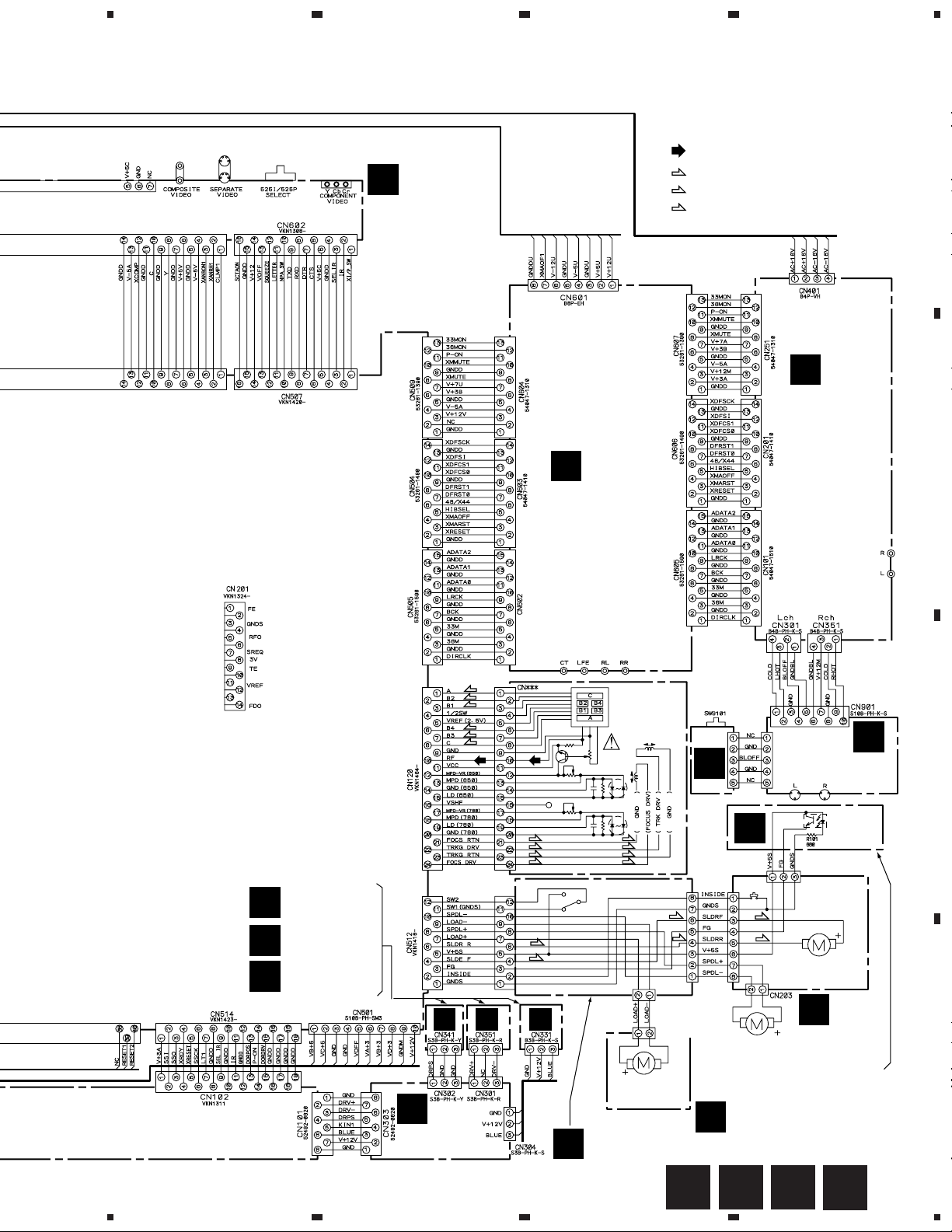
3.3 DVDM ASSY(1/5)
A
E
2/5
CN403
B
S
23
E
E
3/5
VCH1195
E
2/5
E
2/5
VCH1195
4/5
VCH1219
CEHAZA
VCH1220
4
E
3/5
E
2/5
VCH1194
(F)
4
1
VCH1197
(F)
CN402
S
C
PICKUP ASSY
(F)
(F)
VCH1220
VCH1195
VCH1220
E
(F)
(T)
(T)
2/5
(F)
VCH1194
(F)
(T)
(T)
(F)
(S)
(S)
(S)
VCH1197
(F)
2
(T)(T)
E
2/5
3
E
2/5
E
2/5
E
2/5
CN301
D
18
B
1/5
E
1234
VCH1220
(S)
(S)
(T)(F)
VCH1197
(T)
(F)
Page 19
5
678
DV-AX10
E 1/5
RESISTOR
CAPACITOR
DVDM ASSY (VWS1475)
E
3/5
to BY CHIP
BY CHIP
E
4/5
VCH1195
VCH1212
VCH1220
: The power supply is shown with the marked box.
: RF SIGNAL ROUTE
(F)
: FOCUS SERVO LOOP LINE
(T)
: TRACKING SERVO LOOP LINE
(S)
E
4/5
E
3/5
E
4/5
: SLIDER SERVO LOOP LINE
E
2/5
E
2/5
9
5
VCH1194
A
B
(T)
(F)
(S)
(F)
(T)
3 ← 5 CONVERTER
Level Shift
VCH1212
(T)
E
VCH1212
(F)
(S)
(F)
(T)
E
2/5
VCH1219
3/5
to BY CHIP
to BY CHIP
E
3/5
C
E
3/5
D
VCH1197
1/5
E
5
6
7
8
19
Page 20
1
DV-AX10
3.4 DVDM ASSY(2/5)
A
23
E
4/5
E
4/5
VYW1816
E
E
3/5
E
4/5
4
1/5
E
4/5
E
3/5
B
E
3/5
E
3/5
VCH1219
VCH1219
6
4/5
1/5, 5/5
E
E
4/5
E
E
5/5
to BY CHIP
E
4/5
E
4/5
4/5
4/5
E
1/5
A
VCH1219
VCH1219
VCH1219
VCH1219
E
E
5/5
C
E
E
2/5
E
4/5
VCH1219
VCH1219
to BY CHIP
VCH1219
VCH1219
VCH1219
VCH1219
E
3/5
E
1/5
E
3/5
to BY_CHIP
E
1/5
E
E
4/5
D
20
2/5
E
1234
4/5
VCH1219
E
1/5
1/5
VCH1219
E
1/5
E
1/5
E
5/5
E
1/5
E
1/5
E
VCH1195
E
3/5
Page 21
5
E
3/5
to BY_CHIP
VCH1220
678
3 → 5 CONVERTER
VCH1220
VCH1194
E 2/5
CN602
M
E
1/5
DV-AX10
DVDM ASSY (VWS1475)
A
RESISTOR
CAPACITOR
: The power supply is shown with
the marked box.
B
A
to IC601(3P)
E
1/5
E
4/5
E
4/5
5 → 3 CONVERTER
E
E
E
4/5
E
1/5
E
3/5, 4/5
3 → 5 CONVERTER
VCH1220
5/5
4/5
E
4/5
E
3/5
C
to BY CHIP
VCH1220
E
1/5, 3/5, 4/5
CN102
N
E
4/5
E
4/5
E
E
3/5
from BY CHIP
5
6
4/5
E
4/5
E
1/5
2/5
E
7
8
21
D
Page 22
1
DV-AX10
3.5 DVDM ASSY(3/5)
23
4
A
E 3/5
E
B
4/5
DVDM ASSY (VWS1475)
(AC)(AC)
E
4/5
VCH1195
VCH1219
VCH1195
VCH1219
VCH1219
(AC)
(AC)
VCH1219
E
4/5
E
2/5
E
4/5
E
E
E
VCH1219
4/5
4/5
5/5
VCH1219
VCH1195
: RF SIGNAL ROUTE
: CD AUDIO SIGNAL ROUTE
(D)
: DVD AUDIO DATA ROUTE
(AC)
: AC-3/DTS AUDIO DATA ROUTE
E
4/5
VCH1195
VCH1219
E
2/5
E
1/5
(AC)
E
4/5
VCH1219
E
E
VCH1219
1/5
1/5
VCH1195
E
1/5
E
1/5
E
2/5
E
1/5
E
1/5
BY CHIP ES2
2/5
VCH1219
VCH1219
VCH1220
VCH1219
VCH1219
(D)
9
VCH1220
E
4/5
E
1/5
VCH1219
E
4/5
VCH1219
E
4/5
VCH1219
VCH1219
E
2/5
E
2/5
C
E
E
2/5
RESISTOR
CAPACITOR
D
22
3/5
E
1234
Page 23
5
678
DV-AX10
(AC)
(AC)
VCH1195
VCH1195
E
4/5
E
1/5
VCH1195
(AC)
VCH1195
VCH1195
E
VCH1195
2/5
A
B
E
5/5
VCH1220
(CSYNC:FOR EDUCATION)
(PD: FOR EDUCATION)
VCH1220
9
E
4/5
E
VCH1220
9
VCH1195
E
1/5
VCH1220
VCH1220
VCH1195
E
(AC)
E
2/5
4/5
4/5
E
4/5
E
4/5
C
D
3/5
E
5
6
7
8
23
Page 24
1
DV-AX10
3.6 DVDM ASSY(4/5)
23
4
CN103
F 2/2
(D)
E
3/5
from BY CHIP
from BY CHIP
A
VCH1195
VCH1220
VCH1188
VCH1195
VCH1195
VCH1188
B
VCH1197
E
2/5
VCH1194
VCH1195
VCH1188
VCH1197
VCH1220
E
2/5
(D)
VCH1194
VCH1195
E
(D)
2/5
(D)
E
2/5
E
E
from BY CHIP
from BY CHIP
E
3/5
E
F 2/2
CN105
2/5
from BY CHIP
3/5
E
3/5
E
1/5
1/5
E
2/5
E
3/5
from BY CHIP
F 2/2
CN102
(D)
(D)
(D)
(AC)
E
1/5
E
3/5
from BY CHIP
E
3/5
E
2/5
9
VCH1194
(D)
9
E
3/5
E
3/5
E
C
D
(AC)
E
3/5
2/5
E
2/5
3 → 5
CONVERTER
E
to BY CHIP
3/5
E
2/5
(AC)
(AC)
E
LC89055W
-RA8
E
3/5
E
2/5
3/5
(D)
9
to BY CHIP
(AC)
10
10
(D)
(D)
(D)
(AC)
3 → 5
CONVERTER
(D)
3 → 5
CONVERTER
(AC)
TO CN513
E
2/5
VCH1220
(AC)
(D)
(D)
VCH1220
TO CN511
(D)
(D)
(D)
9
E
2/5
24
4/5
E
1234
Page 25
5
678
DV-AX10
VCH1195
VCH1195
VCH1195
E
2/5
E 4/5
VCH1195
VCH1195
DVDM ASSY (VWS1475)
E
2/5
E
2/5
E
2/5
VCH1195
VCH1220
: The power supply is shown with
the marked box.
: CD AUDIO SIGNAL ROUTE
(D)
: DVD AUDIO DATA ROUTE
(AC)
: AC-3/DTS AUDIO DATA ROUTE
RESISTOR
CAPACITOR
VCH1188
VCH1220
8
7
E
3/5
E
3/5
E
1/5, 3/5
& BY CHIP
A
B
G
CN602
E
2/5
TO CN513
VCH1195
E
2/5
E
2/5
E
3/5
E
2/5
from BY CHIP
E
E
2/5
E
2/5
CN801
2/5
E
2/5
E
2/5
E
2/5
L
CN603
G
CN604
G
E
2/5
C
D
E
2/5
4/5
E
5
6
7
8
25
Page 26
1
DV-AX10
3.7 DVDM ASSY(5/5)
23
4
E 5/5
A
B
VCH1195
VCH1195
VCH1195
VCH1195
VCH1195
DVDM ASSY (VWS1475)
(Y)
: Y SIGNAL ROUTE
(C)
: C SIGNAL ROUTE
(CR)
: CR SIGNAL ROUTE
(CB)
: CB SIGNAL ROUTE
RESISTOR
CAPACITOR
VCH1195
VCH1195
C
E
3/5
to BY CHIP
E
2/5
E
D
26
E
2/5
(Y)
E
3/5
5/5
1234
(C)
(C)
(Y)
Page 27
5
678
DV-AX10
: The power supply is shown with the marked box.
A
VCH1194
VCH1194
VCH1188
VCH1194
(CR)
(CB)
(C)
(C)
(C)
(Y)
VCH1194
(C)
E
(Y)
(Y)
2/5
B
(C)(C)
(Y)
(CR)
(CR)
(Y)
(CB)
(Y)
(CR)
(CR)
(CB)
(CB)
(CR)
(CB)
(CR)
(CB)
(Y)
(C)
CN601
E
2/5
(CR)
(CB)
(Y)
M
C
(C)
(CB)
(Y)
(Y)
(Y)
(Y)
(Y)
(Y)
D
(Y)
E
2/5
5/5
E
5
6
7
8
27
Page 28

1
DV-AX10
3.8 DSPB ASSY(1/2)
23
4
A
MASK ROM
F 1/2
DSPB ASSY
(VWG2159)
B
F
2/2
2
(D)
C
F
2/2
F
2/2
to BY CHIP
F
2/2
F
F
2/2
D
2/2
F
2/2
to BY CHIP
F
2/2
(D)
F
2/2
(D)
to BY CHIP
F
2/2
F
2/2
28
to BY CHIP
F
2/2
2/2
F
2/2
to BY CHIP
A
F
2/2
1/2
F
1234
F
2/2
BY CHIP
F
Page 29
5
678
DV-AX10
A
: CD AUDIO SIGNAL ROUTE
(D)
: DVD (AC-3/DTS) AUDIO DATA ROUTE
B
2
(D)
(D)
C
2
F
2/2
F
2/2
(D)
to BY CHIP
F
2/2
(D)
(D)
F
2/2
F
F
(D)
A
F
2/2
F
2/2
2/2
2/2
F
2/2
D
1/2
F
5
6
7
8
29
Page 30

1
DV-AX10
3.9 DSPB ASSY(2/2)
23
F
1/2
F
1/2
4
A
(D)
from BY CHIP
from
BY CHIP
F
F
1/2
F
1/2
F
1/2
E 4/5
CN510
from BY CHIP
B
1/2
from BY CHIP
from BY CHIP
(D)
F
1/2
E 4/5
CN511
F
1/2
1/2
F
F
1/2
from BY CHIP
E 4/5
CN513
from BY CHIP
F
1/2
F
1/2
F
1/2
C
F
1/2
D
F
1/2
1
F
1/2
F
1/2
F
1/2
F
1/2
F
1/2
(D)
F
1/2
2
(D)
(D)
(D)
F
1/2
F
1/2
F
1/2
30
2/2
F
1234
Page 31

5
F 2/2
DSPB ASSY
(VWG2159)
678
DV-AX10
A
: The power supply is shown with the marked box.
: CD AUDIO SIGNAL ROUTE
(D)
: DVD (AC-3/DTS) AUDIO DATA ROUTE
B
3
4
4
F
1/2
C
from BY CHIP
F
1/2
D
2/2
F
5
6
7
8
31
Page 32

1
23
DV-AX10
3.10 MAUD and MAPS ASSYS
4
VNF1084
A
MAUD ASSY
G
(VWV1737)
CN505
(D)
(D)
(D)
(D)
(D)
465
(D)
(D)
(D)
(D)
(D)
(D)
(D)
E 4/5
1
(D)
B
(D)
CN504
(D)
(D)
E 4/5
C
CN509
E 4/5
2
3
D
32
CN101
I
CN201
I
CN251
I
G
1234
Page 33

5
678
DV-AX10
(D)
(D)
(D)
(D)
(D)
: The power supply is shown with
the marked box.
(D)
(D)
(D)
: CD AUDIO SIGNAL ROUTE
(D)
: DVD AUDIO DATA ROUTE
(D)
: DVD (AC-3/DTS) AUDIO SIGNAL ROUTE
7
(D)
7
(D)
7
(D)
A
B
(D)
TO AUDIO TRANS.
MAPS ASSY (VWR1322)
H
VCH1217
VCH1217
7
C
VCH1217
VCH1217
D
CAUTION : FOR CONTINUED PROTECTION AGAINST RISK
OF FIRE, REPLACE ONLY WITH SAME TYPE NO. ICP-N38
ROHM CO.,LTD. FOR IC501, IC511, IC521 AND IC531 .
HG
5
6
7
8
33
Page 34

1
23
DV-AX10
3.11 AUDIO, BLOUT and BLSW ASSYS
AUDIO ASSY (VWV1735)
I
A
5
4
6
CN605
G
4
B
C
CN606
1
2 3
CN607
G
G
TO AUDIO
TRANS.
D
CAUTION : FOR CONTINUED PROTECTION AGAINST RISK
OF FIRE, REPLACE ONLY WITH SAME TYPE NO. ICP-N38
ROHM CO.,LTD. FOR IC421, IC431, IC441 AND IC451 .
34
I
1234
Page 35

5
678
DV-AX10
: The power supply is shown with the marked box.
: CD AUDIO SIGNAL ROUTE
7
7
A
K
BLSW ASSY
(VWG2170)
B
7
J
BLOUT
7
ASSY
(VWV1743)
C
D
JI
5
6
7
K
8
35
Page 36

1
DV-AX10
3.12 DOUT ASSY
A
B
23
4
E 4/5
CN508
C
D
36
L
1234
Page 37

5
DOUT ASSY (VWG2162)
L
678
DV-AX10
A
: The power supply is shown with the marked box.
B
C
D
L
5
6
7
8
37
Page 38

1
DV-AX10
3.13 VOUT ASSY
23
4
VOUT ASSY (VWV1760)
M
A
(C)
(Y)
CN507
E 2/5
B
(Y)
(C)
(Y)
(C)
(Y)
(Y)
(Y)
(C)
(Y)
CN506
E 5/5
C
(CR)
(CB)
D
(CR)
(CB)
(Y)(Y)
(C)
(CR)
(CB)
(CB)
(C)
(CR)
(Y)
(Y)(Y)
(Y)
(CB)
(CR)
38
M
1234
Page 39

5
678
DV-AX10
(C)
(Y)
(C)
(C)
(C)
(C)
: The power supply is shown with the marked box.
A
1
1
(Y)
(Y)
(Y)
(C)
2
(Y)
(C)
2
(Y)
B
3
(Y)
(C)
3
(C)
(Y)
(CB)
(CR)
(Y)
(Y)
(Y)
(CB)
(Y)
(CB)
6
(CR)
4
(Y)
5
C
(CR)
(CB)
(CR)
: VIDEO SIGNAL ROUTE
(Y)
: Y SIGNAL ROUTE
(C)
: C SIGNAL ROUTE
5
(CR)
: CR SIGNAL ROUTE
(CB)
: CB SIGNAL ROUTE
6
D
M
7
8
39
Page 40

1
23
DV-AX10
3.14 FLKB, PLSB, DRMB, DRSB and LEDB ASSYS
A
B
FLKB ASSY (VWG2164)
N
4
FLDIMMER
2
PE5047A
1
C
Red
Red
Red
D
40
N
1234
Page 41

5
678
DV-AX10
P
DRMB ASSY
(VWG2169)
O
PLSB ASSY
(VWG2166)
DRSB ASSY (VWG2168)
Q
Complete
Complete
LEDB ASSY
R
(VWG2167)
A
B
FLKB ASSY
S101 : DIGITAL DATA OFF
S102 : VIDEO OFF
S103 : FLDIMMER
LEVEL SHIFT
: The power supply is shown with the marked box.
PLSB ASSY
S301 : 7/0
S302 : 4
S303 : ¢
S304 : 8
S305 : 3
DRSB ASSY
S341 : DOOR OPEN
S342 : DOOR CLOSE
S301 Linkage
CN514
E 2/5
C
CN404
S
D
N
5
6
7
O
QP
R
8
41
Page 42

1
23
DV-AX10
3.15 SYPS and FANB ASSYS
4
CAUTION : FOR CONTINUED PROTECTION
AGAINST RISK OF FIRE, REPLACE ONLY
A
WITH SAME TYPE NO. 491 1.25, MFD BY
LITTELFUSE INC. FOR IC104.
CAUTION : FOR CONTINUED PROTECTION AGAINST
RISK OF FIRE, REPLACE ONLY WITH SAME TYPE NO.
491 .600, MFD BY LITTELFUSE INC. FOR IC101.
CAUTION : FOR CONTINUED PROTECTION AGAINST
RISK OF FIRE, REPLACE ONLY WITH SAME TYPE NO.
4911.30, MFD BY LITTELFUSE INC. FOR IC216.
CAUTION : FOR CONTINUED PROTECTION AGAINST
RISK OF FIRE, REPLACE ONLY WITH SAME TYPE NO.
4911.25, MFD BY LITTELFUSE INC. FOR IC202.
CAUTION : FOR CONTINUED PROTECTION
AGAINST RISK OF FIRE, REPLACE ONLY
WITH SAME TYPE NO. 491 .500, MFD BY
LITTELFUSE INC. FOR IC102.
B
CAUTION : FOR CONTINUED PROTECTION AGAINST RISK OF FIRE,
REPLACE ONLY WITH SAME TYPE NO. 491007, MFD BY LITTELFUSE
INC. FOR IC106, IC206, IC306 AND IC307.
CAUTION : FOR CONTINUED PROTECTION
AGAINST RISK OF FIRE, REPLACE ONLY
VR206:
V+5U ADJ
CAUTION : FOR CONTINUED PROTECTION
AGAINST RISK OF FIRE, REPLACE ONLY
WITH SAME TYPE NO. 491.900, MFD BY
LITTELFUSE INC. FOR IC302.
WITH SAME TYPE NO. 491.900, MFD BY
LITTELFUSE INC. FOR IC201.
C
TO MAIN TRANS.
CAUTION : FOR CONTINUED PROTECTION
AGAINST RISK OF FIRE, REPLACE ONLY
WITH SAME TYPE NO. 491.600, MFD BY
LITTELFUSE INC. FOR IC301 .
D
CAUTION : FOR CONTINUED PROTECTION AGAINST RISK OF FIRE,
REPLACE ONLY WITH SAME TYPE NO. 491.200, MFD BY LITTELFUSE
INC. FOR IC304, IC314 AND IC324.
42
S
1234
Page 43

5
678
S
CAUTION : FOR CONTINUED PROTECTION AGAINST
RISK OF FIRE, REPLACE ONLY WITH SAME TYPE NO.
491 .600, MFD BY LITTELFUSE INC. FOR IC103.
DV-AX10
SYPS ASSY (VWR1324)
A
CN501
E 1/5
CAUTION : FOR CONTINUED PROTECTION AGAINST
RISK OF FIRE, REPLACE ONLY WITH SAME TYPE NO.
4911.25, MFD BY LITTELFUSE INC. FOR IC203.
CAUTION : FOR CONTINUED PROTECTION AGAINST
RISK OF FIRE, REPLACE ONLY WITH SAME TYPE NO.
V+7U1
491.400, MFD BY LITTELFUSE INC. FOR IC303.
W150 W151
CAUTION : FOR CONTINUED PROTECTION
AGAINST RISK OF FIRE, REPLACE ONLY
WITH SAME TYPE NO. 491 .500, MFD BY
LITTELFUSE INC. FOR IC332.
CAUTION : FOR CONTINUED PROTECTION
AGAINST RISK OF FIRE, REPLACE ONLY
WITH SAME TYPE NO. 491 .800, MFD BY
LITTELFUSE INC. FOR IC204 AND IC322.
B
CN502
E 1/5
C
N
CN103
FAN MOTOR
D
FANB ASSY
T
(VWR1325)
S
5
6
7
T
8
43
Page 44

DV-AX10
WAVEFORMS
Note : The encircled numbers denote measuring point in the schematic diagram.
DVDM ASSY
CN201 - pin 5, 6 (RFO)
1
V: 1V/div. H: 50nsec/div.
(at DVD PLAY)
CN201 - pin 9, 10 (TE)
2
V: 1V/div. H: 5msec/div.
(at DVD PLAY)
CN201 - pin 13, 14 (FDO)
3
V: 1V/div. H: 5msec/div.
(at DVD PLAY)
Foot of R612 (20M)
6
V: 1V/div. H: 20nsec/div.
(at DVD PLAY)
GND
Foot of R981 (16M)
7
V: 1V/div. H: 20nsec/div.
(at DVD PLAY)
GND
Foot of R973 (27M)
8
V: 1V/div. H: 10nsec/div.
(at DVD PLAY)
Compression DATA
10
CH1 : Foot of R6010
CH2 : Foot of R6011
V: 1V/div. H: 2µsec/div.
[at DVD (AC-3, DTS) PLAY]
GND
GND
CH2
GND
CH1
(trigger)
GND
DSPB ASSY
Foot of R140 (HCKT)
1
V: 1V/div. H: 20nsec/div.
[at DVD-A (48k, 96k, 192k) PLAY]
DVD-A DATA
2
CH1 : Foot of R135→Foot of R257
→Foot of R148
CH2 : IC101 - pin 4,5,6→
IC201 - pin 4,5,6
V: 2V/div. H: 2µsec/div.
[at DVD-A (48k, 5.1ch) PLAY]
IC801 - pin 81 (SED0)
3
V: 1V/div. H: 50nsec/div.
(at SACD PLAY)
GND
CH2
GND
CH1
(trigger)
GND
CN201 - pin 1, 2 (FE)
4
V: 100mV/div. H: 5msec/div.
(at DVD PLAY)
IC201 - pin 1 (EFMOUT)
5
V: 1V/div. H: 5msec/div.
(at DVD PLAY)
44
GND
CD DATA
9
CH1 : IC201 - pin 5→IC701 - pin 110
→IC801 - pin 81→IC904 - pin 5
→Foot of R913
CH2 : IC201 - pin 3→IC701 - pin 111
→IC801 - pin 71→IC901 - pin 5
→IC902 - pin 4→Foot of R912
V: 1V/div. H: 2µsec/div.
(at CD PLAY)
GND
GND
GND
CH2
GND
CH1
(trigger)
GND
Foot of R803 (DSDL)
4
Foot of R804 (DSDR)
V: 1V/div. H: 200nsec/div.
(at SACD PLAY)
GND
GND
Page 45

DV-AX10
MAUD ASSY
Foot of R620 (DIRCLK)
1
V: 1V/div. H: 20nsec/div.
Foot of R622 (36M)
2
V: 1V/div. H: 20nsec/div.
Foot of R621 (33M)
3
V: 1V/div. H: 20nsec/div.
IC603 - pin 4 (ADATA1)
6
IC603 - pin 2 (ADATA2)
(44.1kHz/24 bit)
V: 1V/div. H: 2µsec/div.
GND GND
IC741 - pin 7, IC751 - pin 7,
7
IC761 - pin 7, IC771 - pin 7
(Analog Output)(44.1kHz/24 bit)
V: 1V/div. H: 500µsec/div.
GND
BCK, LRCK, ADATA (44.1kHz/24 bit)
8
V: 5V/div. H: 2µsec/div.
GND
AUDIO ASSY
Foot of R108 (DIRCLK)
1
V: 1V/div. H: 20nsec/div.
Foot of R124 (36M)
2
V: 1V/div. H: 20nsec/div.
Foot of R114 (33M)
3
V: 1V/div. H: 20nsec/div.
IC131 - pin 14 (DATA1)(44.1kHz/24 bit)
6
V: 1V/div. H: 2µsec/div.
GND GND
IC311 - pin 7, IC331 - pin 7 ,
7
IC361 - pin 7, IC381 - pin 7
(Analog Output)(44.1kHz/24 bit)
V: 1V/div. H: 500µsec/div.
GND
BCK, LRCK, ADATA (44.1kHz/24 bit)
8
V: 5V/div. H: 2µsec/div.
GND
IC603 - pin 8 (BCK1)(44.1kHz/24 bit)
4
V: 1V/div. H: 200msec/div.
IC603 - pin 6 (LRCK1)(44.1kHz/24 bit)
5
V: 1V/div. H: 5µsec/div.
GND
GND
GND
BCK
GND
LRCK
GND
ADATA
GND
IC131 - pin 15 (BCK1)(44.1kHz/24 bit)
4
V: 1V/div. H: 200msec/div.
IC131 - pin 14 (LRCK1)(44.1kHz/24 bit)
5
V: 1V/div. H: 5µsec/div.
GND
GND
GND
BCK
GND
LRCK
GND
ADATA
GND
45
Page 46

DV-AX10
VOUT ASSY
JA651 - pin 1, 2
1
(Composite Video Out)
at play Composite Video Disc
(DVD-REF-A1 : T2-Chap. 1)
V: 200mV/div. H: 10µsec/div.
JA652 - pin 3, 9 (Y Output)
2
at play Composite Video Disc
(DVD-REF-A1 : T2-Chap. 1)
V: 200mV/div. H: 10µsec/div.
JA652 - pin 4, 10 (C Output)
3
at play Composite Video Disc
(DVD-REF-A1 : T2-Chap. 1)
V: 200mV/div. H: 10µsec/div.
JA653 - pin 6 (Cr Output)
6
at play Color Bar Signal
(DVD-REF-A1 : T2-Chap. 19)
V: 200mV/div. H: 5µsec/div.
GND
GND
FLKB ASSY
IC101 - pin 11 (X2)
1
V: 1V/div. H: 100nsec/div.
GND
IC101 - pin 21 (XRDY)
2
V: 1V/div. H: 20msec/div.
GND
GND
JA653 - pin 2 (Y Output)
4
at play Color Bar Signal
(DVD-REF-A1 : T2-Chap. 19)
V: 200mV/div. H: 5µsec/div.
JA653 - pin 3 (Cb Output)
5
at play Color Bar Signal
(DVD-REF-A1 : T2-Chap. 19)
V: 200mV/div. H: 5µsec/div.
GND
GND
GND
46
Page 47

1
234
4. PCB CONNECTION DIAGRAM
DV-AX10
NOTE FOR PCB DIAGRAMS :
1. Part numbers in PCB diagrams match those in the schematic
diagrams.
2. A comparison between the main parts of PCB and schematic
diagrams is shown below.
Symbol In PCB
Diagrams
BCE
BCE
D
Symbol In Schematic
Diagrams
BCEBCE
BCE
DGGSS
BCE
DGS
Part Name
Transistor
Transistor
with resistor
Field effect
transistor
Resistor array
3-terminal
regulator
4.1 LOMB, LOSB, SMEB and FGSB ASSYS
3. The parts mounted on this PCB include all necessary parts for
several destinations.
For further information for respective destinations, be sure to
check with the schematic diagram.
4. View point of PCB diagrams.
Connector
Capacitor
SIDE A
P.C.Board
Chip Part
SIDE B
A
B
LOSB ASSY
B
(VNP1628-A)
CARRIAGE
MOTOR
M
(VNP1695-A)
SMEB ASSY
C
CN512
E
M
SPINDLE
MOTOR
SIDE A
PC101
R101
LOMB ASSY
A
(VNP1628-A)
FGSB ASSY
D
LOADING
MOTOR
C
(VNP1661-B)
D
DCBA
1
2
3
4
47
Page 48

1
DV-AX10
4.2 DVDM ASSY
A
E
CN602
M
B
DVDM ASSY
23
G
CN604
G
CN603
G
CN602
4
PICKUP
ASSY
CN402
S
CN601
M
C
CN801
L
VR1261 VR1251 VR1201 VR1331
D
IC1008
48
IC1009
E
1234
Q1631 IC1201
IC1631
Q1661
IC6001
IC1691
Q1261
Q1362
Q1313 Q1312
Q1463 Q1462
Q1413 Q1412
Q1563 Q1562
Q1513 Q1512
Q1301 IC911
VR1431
VR1532
VR1531
Q1401
Q1501
IC609
IC905
IC987
IC988
IC983
IC1007
IC1006
IC901
IC607
IC902
IC915
IC916
IC904
IC906
IC1001
IC801
IC913
IC914
IC704
Page 49

5
678
DV-AX10
A
P
B
Y
CN301
• This PCB is a six-layered board.
CN403
S
B
N
CN102
C
Q113
IC704 Q281
Q108
IC261
IC302
Q105
IC303
5
IC201
IC702
IC703
Q114
IC614
Q101
Q103
IC251
IC965
IC5001
IC610
IC959
IC951
6
IC252
Q952
IC601
IC603
IC253
Q951
(VNP1749-C)
SIDE A
Q602 Q601IC352
E
7
8
49
D
Page 50

A
B
1
DV-AX10
DVDM ASSY
E
23
4
C
IC501
IC608
D
50
E
1234
IC606
IC611
IC613
Q542
Q541
Q543
IC612
IC604
IC615
Q102
CN103
F
IC299
Q109
IC101
Q112
Q107
Q111
Q106
Q301
IC701
IC305
IC301
IC161
CN105
IC1012
IC1011II
F
Page 51

5
678
DV-AX10
CN102
F
• This PCB is a six-layered board.
A
B
IC1012
IC1011
IC903
IC912
Q1001
IC1002
IC802
5
IC1003
IC803
IC917
IC1004
IC804
IC1005
Q1251
Q1201
Q1311
Q1531
IC909
6
Q1700
Q1701
Q1363
IC1602
Q1411
Q1511
Q1702
Q1703
IC1601
IC1603
IC907
IC1010
C
(VNP1749-C)
D
SIDE B
E
7
8
51
Page 52

1
DV-AX10
4.3 DSPB ASSY
A
DSPB ASSY
F
B
23
• This PCB is a four-layered board.
IC106 IC802 IC801
IC803
IC165 IC161 IC152 IC158
IC164 IC156 IC105
4
IC951 IC102 IC503
IC151 IC504 IC551
IC552
IC553 IC554 IC555
IC931 IC201
IC501
IC162
C
IC502
IC921
IC104
IC911 IC153
IC101
IC1101
IC160
IC901 IC157
IC601
IC154
D
(VNP1750-B)
SIDE A
52
F
1234
Page 53

1
DSPB ASSY
F
234
DV-AX10
A
• This PCB is a four-layered board.
E
CN511
B
E
CN513
E
CN510
C
(VNP1750-B)
D
SIDE B
F
1
2
3
4
53
Page 54

1
BlackBlackBlackBlack
MAUD ASSY
G
Q701
Q702
IC741
IC751
IC761
IC771
IC701
IC711
IC721
IC731
CN502
H
DV-AX10
4.4 MAUD ASSY
A
B
23
4
C
D
54
G
1234
Page 55

5
678
DV-AX10
A
B
CN101
I
701
711
721
731
Q113
IC201
IC702
IC703
Q114
IC614
Q101
Q103
IC251
IC965
IC5001
IC610
Q281
IC959
IC951
IC252
Q952
IC601
IC603
IC253
Q951
CN505
E
CN201
I
CN504
E
CN251
I
CN509
E
(VNP1751-D)
Q602IC352
C
D
SIDE A
G
5
6
7
8
55
Page 56

DV-AX10
MAUD ASSY
G
Q607
Q606
Q601
Q602
A
B
1
23
4
C
D
56
G
1234
Page 57

5
678
DV-AX10
A
B
C
(VNP1751-D)
D
SIDE B
G
5
6
7
8
57
Page 58

1
DV-AX10
4.5 MAPS ASSY
A
Q503
IC501
IC521
IC502
B
Q522
MAPS ASSY
H
23
4
Open
Q532
IC503
IC531
IC511
C
Q513
AUDIO
TRANS
(VNP1766-D)
CN601
G
D
SIDE A
58
H
1234
Page 59

1
MAPS ASSY
H
234
DV-AX10
A
Q502
B
(VNP1766-D)
Q501
Q521
Q504
Q511
Q505
Q531
Q512
C
D
SIDE B
H
1
2
3
4
59
Page 60

1
23
DV-AX10
4.6 AUDIO, BLOUT and BLSW ASSYS
A
AUDIO ASSY
I
Red
B
4
White
C
Q323
IC392
IC342
D
BLOUT ASSY
J
IC391
IC341
(VNP1766-D)
IC381
IC361
IC351
IC311
BLSW ASSY
K
(VNP1766-D)
IC371
IC351
IC321
IC301
60
I J K
1234
Page 61

5
678
DV-AX10
G
CN607
G
CN606
G
CN605
AUDIO
TRANS
A
B
VC111
VC121
VC111
VC121
IC101
IC171
IC131
IC111
IC121
IC271
IC272
Q223
Q224
Q221
IC151
Q262
Q264
Q263
Q222
C
(VNP1751-D)
IC261IC141
IC421
Q422
Q432
Q452
Q442
IC441
IC431
IC451
IC422
IC442
D
SIDE A
61
I
5
6
7
8
Page 62

A
B
1
DV-AX10
AUDIO ASSY
I
23
4
C
Q413
Q414
D
Q421
Q431
Q451
Q441
SIDE B
62
I
1234
Page 63

5
678
DV-AX10
A
B
BLSW ASSY
K
(VNP1766-D)
5
Q386
Q366
Q335
Q336
Q316
Q315
6
Q322
BLOUT ASSY
J
Q371
Q321
Q312
C
(VNP1751-D)
Q362Q365 Q385
D
(VNP1766-D)
KJI
7
8
63
Page 64

1
DV-AX10
4.7 DOUT ASSY
23
4
A
B
DOUT ASSY
L
IC931 IC851
IC901
Q941
IC911
Q943
Q942
IC921
IC841
IC831
IC871
Q861
Q831
IC881
IC861
IC821
(VNP1751-D)
Q865
Q864
Q863
Q862
IC811
E
CN508
SIDE A
C
D
DOUT ASSY
L
64
(VNP1751-D)
SIDE B
L
1234
Page 65

1
4.8 VOUT ASSY
VOUT ASSY
M
234
DV-AX10
A
B
VOUT ASSY
M
Q603
Q604
E
IC601
Q602
Q601
CN507
IC831
IC871
IC604
IC602
Q608
SIDE A
IC605
Q613
E
IC603 Q611
CN506
Q609
IC607
IC610
Q615
Q506
IC609
Q614
Q502
Q501
(VNP1752-A)
Q503
IC606
Q504
IC608
Q513
IC501
C
(VNP1752-A)
Q505Q616Q610Q612Q552Q551Q605
D
SIDE B
M
1
2
3
4
65
Page 66

1
3
23
DV-AX10
4.9 FLKB, PLSB, DRMB, DRSB and LEDB ASSYS
4
A
FLKB ASSY
N
B
S
CN404
CN514
E
Q104 IC10
IC106
IC107
Q106
Q105
PLSB ASSY
O
C
DRMB ASSY
LEDB ASSY
R
D
P
Q109Q110 IC102
(VNP1752-A)
DRSB ASSY
Q
66
(VNP1752-A)
(VNP1752-A)
(VNP1752-A)
PON Q R
1234
Page 67

5
A
678
DV-AX10
A
IC106
4 IC103 IC105 IC101
IC107
(VNP1752-A)
B
C
Y
D
)
5
6
SIDE A
N
7
8
67
Page 68

A
O
B
1
DV-AX10
FLKB ASSY
N
23
4
Q114
C
D
SIDE B
68
N
1234
Page 69

5
678
DV-AX10
A
SIDE B
PLSB ASSY
O
Q108
Q103 Q101
Q102
Q112
(VNP1752-A)
(VNP1752-A)
B
C
DRSB ASSY
Q
(VNP1752-A)
5
DRMB ASSY
P
6
(VNP1752-A)
LEDB ASSY
R
(VNP1752-A)
PON Q R
7
8
69
D
Page 70

1
DV-AX10
4.10 SYPS ASSY
23
4
S
SYPS ASSY
A
B
IC106
IC307
IC206
IC306
IC303
IC313
IC304
Q304
IC302
IC301
IC312
W150
W151
MAIN
TRANS
IC204
IC201
IC216
Q331 IC104 Q206
IC202
IC212
VR206
IC311 IC103 IC102
IC203
IC311
T
C
IC213
IC113 IC101
IC211
IC112
IC214
IC111
CN702
D
E
IC322
IC332
N
CN103
CN502
E
CN501
70
MAIN
TRANS
IC324 IC314
S
1234
SIDE A
(VNP1766-D)
Page 71

S
SYPS
ASSY
1
234
DV-AX10
A
B
SIDE B
C
Q218
Q401 Q402
D
(VNP1766-D)
S
1
2
3
4
71
Page 72

1
DV-AX10
4.11 FANB and LSFB ASSYS
LSFB ASSY
U
A
FANB ASSY
T
CN405
S
B
23
4
AC
POWER
CORD
MAIN
TRANS
AUDIO
TRANS
(VNP1751-D)
FAN MOTOR
(VNP1751-D)
C
FANB ASSY
T
SIDE A
(VNP1751-D)
D
U
72
LSFB ASSY
SIDE B
T U
1234
(VNP1751-D)
Page 73

DV-AX10
Mark No. Description Part No.
5. PCB PARTS LIST
NOTES : ÷ Parts marked by “ NSP ” are generally unavailable because they are not in our Master Spare Parts List.
÷ The
÷ When ordering resistors, first convert resistance values into code form as shown in the following examples.
Mark No. Description Part No. Mark No. Description Part No.
mark found on some component parts indicates the importance of the safety factor of the part.
Therefore, when replacing, be sure to use parts of identical designation.
Ex. 1 When there are 2 effective digits (any digit apart from 0), such as 560 ohm and 47k ohm (tolerance is shown by
J = 5%, and K = 10%).
560 Ω = 56 × 10
47k Ω = 47 × 10
0.5 Ω = R50 ...................................................................... RN2H Â 5 0 K
1 Ω = 1R0 ......................................................................... RS1P 1 Â 0 K
Ex. 2 When there are 3 effective digits (such as in high precision metal film resistors).
5.62k Ω = 562 × 10
1
= 561................................................... RD1/4PU 5 6 1 J
3
= 473 .................................................. RD1/4PU 4 7 3 J
1
= 5621 ........................................... RN1/4PC 5 6 2 1 F
LIST OF PCB ASSEMBLIES
NSP LOAB ASSY VWM1798
NSP LOMB ASSY VWG1886
NSP LOSB ASSY VWG1885
NSP SMEB ASSY VWG2048
NSP FGSB ASSY VWG2009
NSP MADOUT ASSY VWM1982
Traverse Mechanism Assy-S VXX2653
DVDM ASSY VWS1475
DSPB ASSY VWG2159
AUDIO ASSY VWV1735
MAUD ASSY VWV1737
DOUT ASSY VWG2162
Mark No. Description Part No.
OTHERS
CN303 KR CONNECTOR B2B-PH-K-S
CN302 8P FFC CONNECTOR VKN1268
CN301 12P FFC CONNECTOR VKN1272
SMEB ASSY
C
SWITCH
S201 Push SW DSG1016
OTHERS
CN201 3P FFC CONNECTOR 52044-0345
CN202 8P FFC CONNECTOR VKN1212
PC BOARD(SMEB) VNP1695
NSP SYLF ASSY VWM1989
NSP BLOUT ASSY VWV1743
NSP BLSW ASSY VWG2170
NSP FANB ASSY VWR1325
NSP FLOUT ASSY VWM1984
NSP LEDB ASSY VWG2167
NSP DRSB ASSY VWG2168
NSP DRMB ASSY VWG2169
MAPS ASSY VWR1322
SYPS ASSY VWR1324
LSFB ASSY VWR1320
FLKB ASSY VWG2164
PLSB ASSY VWG2166
VOUT ASSY VWV1760
LOAB ASSY
OTHERS
PC BOARD (LOAB) VNP1628
LOMB ASSY
A
OTHERS
CN401 KR CONNECTOR B2B-PH-K-S
LOSB ASSY
B
SWITCH
S301 VSK1011
FGSB ASSY
D
SEMICONDUCTOR
PC101 GP2S60
RESISTOR
R101 RS1/10S331J
DVDM ASSY
E
SEMICONDUCTOR
IC301 ADC08351CIMTC
IC261, IC302 BA4510F
IC352 BA5982FP
IC251 BA6195FP
IC959 BU2185F
IC1003 CXD2307R
IC965 CY2071ASL-371
IC702 HY51V65804ASLTC-50
IC1002 HY58163210TQ-10F
IC101 LA9701M
IC201 LC78652W
IC6001 LC89055W-RA8
IC802 M2V64S40BTP-8L
IC803, IC804 M5M4V18165DTP-6S
IC801 M65774FP
IC601 PD3410A
IC701 PE5220A
IC5001 PE9008A
IC1001 PM0024AF
IC604 TC55V1001AF8
73
Page 74

DV-AX10
Mark No. Description Part No. Mark No. Description Part No.
IC907, IC909 TC74VHC153FT
IC902, IC905 TC74VHC157FT
IC612 TC74VHC541FT
IC607, IC610 TC74VHC574FT
IC617 TC74VHC74FT
IC608, IC609, IC611, IC906 TC74VHCT541AFT
IC161, IC913–IC916, IC983 TC7SET08FU
IC987, IC988 TC7SET32FU
IC1005 TC7SH02FU
IC1008,IC613, IC614, IC912 TC7SH04FU
IC1006,IC1009,IC1010,IC917 TC7SH08FU
IC1011,IC1012 TC7SH14FU
IC1007,IC606, IC703 TC7SH32FU
IC299, IC615, IC616 TC7SZ32FU
IC1601-IC1603,IC252, IC253 TC7W53FU
IC501 TC7WH126FU
IC901, IC904, IC911 TC7WH157FU
IC303, IC903, IC951 TC7WHU04FU
IC305 TK15404M
IC1201,IC1631,IC1691 TK15420M
IC603 VYW1816
Q 109, Q 1312,Q 1362,Q 1412,Q 1462 2SA1576A
Q 1512,Q 1562,Q 301 2SA1576A
Q 105, Q 114, Q 1311,Q 1313,Q 1363 2SC4081
Q1411, Q1413, Q1463, Q1511,Q1513 2SC4081
Q 1563,Q 603 2SC4081
Q 602, Q 951 DTA114EUA
Q 1701,Q 1703 DTA143EUA
Q 1001,Q 107, Q 111, Q 601, Q952 DTC114EUA
Q 1700,Q 1702 DTC143EUA
Q 108 HN1K03FU
Q 102, Q 106 IMT1A
Q 101 IMX1
Q 1201,Q 1251,Q 1301,Q 1401,Q 1501 IMZ1A
Q 112, Q 113 UMX1N
Q 103, Q 281, Q 542, Q 543 UMZ1N
D 302 KV1470
D 601 RB501V-40
COILS AND FILTERS
L1001- L1010 LCYA100J2520
L304 LCYA1R5J2520
L 101, L 330 LCYA8R2J2520
F1201,F1251, F1361, F1461, F1561 VTF1150
F 1311,F 1411,F 1511 VTF1151
F401– F413 VTH1040
L1011, L102, L1020, L 201– L204 VTL1124
L 251, L 301, L 302, L 305 VTL1124
L 351, L 352, L 5001,L 6001, L6002 VTL1124
L 601, L 701– L703, L 801– L805 VTL1124
L 9001,L 9003,L 9004,L 9010,L959 VTL1124
L 965, L 991, L 992 VTL1124
CAPACITORS
C 612 CCSRCH100D50
C 1070– C1072, C1085, C1086 CCSRCH101J50
C 1090, C1091, C123, C145, C258 CCSRCH101J50
C 282, C 617, C643, C655 CCSRCH101J50
C 661– C664, C666– C668 CCSRCH101J50
C 727, C728, C935– C939, C984 CCSRCH101J50
C1113, C216, C313 CCSRCH102J50
C126, C 333, C 634– C642, C665 CCSRCH150J50
C981, C 982 CCSRCH150J50
C 206, C 210, C211 CCSRCH151J50
C 322 CCSRCH180J50
C104– C108, C116, C151, C314 CCSRCH220J50
C152 CCSRCH221J50
C 632 CCSRCH330J50
C 209, C 283, C 360, C 391, C 392 CCSRCH331J50
C 584, C 656 CCSRCH331J50
C 128, C 134, C 297, C 335 CCSRCH470J50
C 122, C 208, C 352 CCSRCH471J50
C127, C 334, C6009, C6010, C953 CCSRCH5R0C50
C124, C146 CCSRCH680J50
C117, C240 CCSRCH681J25
C1370, C1470, C1570, C952 CCSRCJ3R0C50
C454 CEHAZA101M16
C115, C 450– C 453 CEHAZA471M6R3
C1087, C1088 CEV100M35
C1029,C 1084,C 1092,C 1201,C 1203 CEV101M10
C1301,C 1303,C 1401,C 1403,C 1501 CEV101M10
C1503,C 5004,C 645, C 733 CEV101M10
C113, C 139 CEV220M16
C1634, C1636, C6013 CEV220M6R3
C1003 CEV221M4
C111, C301, C409, C6007 CEV470M6R3
C140, C223, C224, C252, C264 CKSQYB105K10
C312 CKSQYB105K10
C1009- C1012, C1015, C1016 CKSQYF105Z16
C1019- C1021, C1026, C1027 CKSQYF105Z16
C1082, C1083, C114, C125, C148 CKSQYF105Z16
C150, C 217, C 236, C 299, C 367 CKSQYF105Z16
C431– C442, C5002, C5003, C561 CKSQYF105Z16
C581, C582, C621, C625, C628 CKSQYF105Z16
C647, C648, C903, C913 CKSQYF105Z16
C1005- C1008, C1030, C1033- C1036 CKSQYF225Z16
C1039- C1046, C1051- C1056 CKSQYF225Z16
C1093- C1096, C302, C305 CKSQYF225Z16
C327, C328, C585 CKSQYF225Z16
C203, C220, C225, C239, C256 CKSRYB103K50
C320, C321, C362, C363, C502 CKSRYB103K50
C6002, C6005, C619, C722 CKSRYB103K50
C101, C1017, C1018, C118– C120 CKSRYB104K16
C212, C213, C227, C 228, C231 CKSRYB104K16
C263, C315– C317, C332, C359 CKSRYB104K16
C369, C370, C418, C420 CKSRYB104K16
C6003, C6004, C609, C716 CKSRYB104K16
C281 CKSRYB222K50
C153, C266 CKSRYB223K50
C229 CKSRYB224K10
C261, C351 CKSRYB332K50
C214, C251, C354 CKSRYB472K50
C330 CKSRYB682K50
C133, C136, C355, C356, C703 CKSRYF103Z50
C102, C1063- C1068, C1073, C121 CKSRYF104Z16
C138, C308, C310, C713, C717 CKSRYF104Z16
C933 CKSRYF104Z16
C1059, C1062, C1077- C1081, C1089 CKSRYF105Z10
C109, C110, C1111, C1112, C1202 CKSRYF105Z10
C1204, C1252, C1254, C1257, C1259 CKSRYF105Z10
C130, C1302, C1304, C131, C1331 CKSRYF105Z10
C1402, C1404, C143, C1431, C1502 CKSRYF105Z10
74
Page 75

DV-AX10
Mark No. Description Part No.
C1504, C1531, C1602, C1605- C1609 CKSRYF105Z10
C161, C1633, C1635, C1693, C1695 CKSRYF105Z10
C 202, C 204, C 215, C 221, C 222 CKSRYF105Z10
C 226, C 230, C 235, C 253, C 255 CKSRYF105Z10
C 257, C 265, C 298, C 303 CKSRYF105Z10
C 306, C 307, C 309, C 319, C 329 CKSRYF105Z10
C 371, C 372, C 402, C 404, C 406 CKSRYF105Z10
C 408, C 410, C 412, C 414, C 416 CKSRYF105Z10
C 422, C 424, C 426, C 501 CKSRYF105Z10
C542, C543, C6001, C6006, C6008 CKSRYF105Z10
C6011, C6012, C6014, C602– C608 CKSRYF105Z10
C 610, C 611, C 613– C616, C 618 CKSRYF105Z10
C622– C624, C 626, C 627, C 631 CKSRYF105Z10
C646– C648, C 651– C654, C 702 CKSRYF105Z10
C704– C712, C 714, C 718– C721 CKSRYF105Z10
C723– C726, C734, C771, C772 CKSRYF105Z10
C806– C818, C 822, C 827, C 829 CKSRYF105Z10
C831– C836, C 838– C841 CKSRYF105Z10
C 901, C 902, C 904, C 906, C 907 CKSRYF105Z10
C 909, C 911, C 914– C916, C 918 CKSRYF105Z10
C 921– C923, C 927, C 931, C 932 CKSRYF105Z10
C 934, C 951, C 960, C 961, C 966 CKSRYF105Z10
C 983, C 987, C 988 CKSRYF105Z10
C 357 CKSRYF223Z50
C1058, C1061, C1074, C1075, C129 VCH1188
(68µF/6.3V)
C149, C401 (68µF/6.3V) VCH1188
C413, C415, C5001 (68µF/6.3V) VCH1188
C1058, C1061, C1075, C1092, C129 VCH1194
(100µF/6.3V)
C149, C201, C403, C405, C645 VCH1194
(100µF/6.3V)
C 912 (100µF/6.3V) VCH1194
C1002, C1014, C1023, C1024, C1038 VCH1195
(150µF/4V)
C1048, C1049, C1084, C142, C147 VCH1195
(150µF/4V)
C205, C326, C407, C411, C421 VCH1195
(150µF/4V)
C423, C499, C5004, C601, C633 VCH1195
(150µF/4V)
C715, C731– C733, C773 VCH1195
(150µF/4V)
C801– C803, C823, C826 VCH1195
(150µF/4V)
C851– C853, C955, C959, C965 VCH1195
(150µF/4V)
C991– C993 (150µF/4V) VCH1195
C 254, C 358, C 368, C 417, C 419 VCH1197
(33µF/16V)
C427 (33µF/16V) VCH1197
C1258, C1260, C1694, C1696, C207 VCH1212
(47µF/6.3V)
C37, C304 (47µF/6.3V) VCH1212
C265, C319, C602– C608 (2.2µF) VCH1219
C610, C611, C613– C616, C654 VCH1219
C702, C704– C712, C718 (2.2µF) VCH1219
C720, C721, C724, C725, C734 VCH1219
C114, C125, C150, C218, C367 VCH1220
(10µF)
C434, C435, C5002, C5003, C561 VCH1220
(10µF)
C625, C628, C701, C714, C723 VCH1220
(10µF)
Mark No. Description Part No.
C804, C811, C813, C816, C818 VCH1220
(10µF)
C903, C913 (10µF) VCH1220
VC951 (20pF) VCM1008
RESISTORS
R 738 RAB4C100J
R 381, R 543, R 545, R 594, R 613 RAB4C103J
R 637, R 648, R 649, R 691, R 692 RAB4C103J
R 707, R 715, R 716 RAB4C103J
R 1053- R1055, R121, R595 RAB4C220J
R 609, R 610, R 616, R 617 RAB4C220J
R 733, R 734, R 736– R741, R851 RAB4C220J
R 853, R 855, R 860, R 863 RAB4C220J
R 867– R873, R 876, R 877 RAB4C220J
R 123 RAB4C390J
R 6017,R 602, R 605– R608 RAB4C470J
R1069- R1073, R1076, R143, R173 RS1/10S0R0J
R 401, R 402, R406– R409, R416 RS1/10S0R0J
R 596 RS1/10S0R0J
R 1691 RS1/16S1002F
R1206, R1256, R1314, R1364, R1414 RS1/16S1501F
R 1464, R1514, R1564, R232 RS1/16S1501F
R 365, R 398 RS1/16S1503F
R 1259 RS1/16S1801F
R 1077- R1079 RS1/16S1802F
R 1301, R1401, R1501 RS1/16S2000F
R 1210, R1694 RS1/16S2201F
R 1207 RS1/16S2202F
R1220, R1270, R1320, R1370, R1420 RS1/16S2701F
R 1470,R 1520,R 1570 RS1/16S2701F
R1058, R1205, R1255, R1313, R1363 RS1/16S3300F
R1413, R1463, R1513, R1563, R228 RS1/16S3300F
R332 RS1/16S3300F
R1065- R1067, R1260 RS1/16S3901F
R1693 RS1/16S5601F
R1257 RS1/16S6802F
R361, R399 RS1/16S7502F
R1209 RS1/16S9100F
VR1201, VR1251, VR1331 (470Ω) VCP1182
VR1431, VR1531 (470Ω) VCP1182
Other Resistor RS1/16S&&&J
OTHERS
X601 CERAMIC RESONATOR DSS1110
(20MHz)
X951 CERAMIC RESONATOR VSS1086
(27.0MHz)
X6001 CERAMIC RESONATOR VSS1144
(12.2888MHz)
CN509 CONNECTER 53261-1390
CN504 CONNECTER 53261-1490
CN505,CN508 CONNECTER 53261-1590
CN501 KR CONNECTER S10B-PH-SM3
CN502 PH CONNECTER S8B-PH-SM3
CN201 B TO CONNECTER14P VKN1324
CN512 12P FFC CONNECTER VKN1416
CN507 16P FFC CONNECTER VKN1420
CN514 19P FFC CONNECTER VKN1423
CN506 28P FFC CONNECTER VKN1432
CN120 24P FFC CONNECTER VKN1464
CN511 B TO CONNECTER 30P VKN1569
CN510,CN513 CONNECTER40P VKN1570
75
Page 76

DV-AX10
Mark No. Description Part No. Mark No. Description Part No.
KN1-KN4 EARTH METAL FITTING VNF1109
DSPB ASSY
F
SEMICONDUCTORS
IC501,IC502 CS8404A-CS
IC801 CXD2751Q
IC802 KM48V8104CS-6
IC901,IC931 KM616V1002CT-12
IC921 PDK038A
IC911,IC951 TC55V8128BJ-12
IC503,IC551 TC74LCX74FT
IC152,IC156,IC157,IC161,IC162 TC74VHC157FT
IC153,IC160 TC74VHC595FT
IC104 TC7SET08FU
IC106,IC154,IC165 TC7SH04FU
IC552,IC556 TC7SH86FU
IC504 TC7WH00FU
IC105 TC7WH04FU
IC158,IC555 TC7WH125FU
IC151,IC164,IC553,IC554 TC7WH157FU
IC102 TC7WH74FU
IC601 TC7WU04F
IC101,IC201 XCD56362PV100
RESISTORS
R101,R108,R139,R143,R145(10kΩ) DCN1094
R148,R207,R217 (10kΩ) DCN1094
R110,R119,R123,R163,R164 (22Ω) DCN1104
R172,R173,R178,R180,R197 (22Ω) DCN1104
R216,R219,R230,R238,R239 (22Ω) DCN1104
R244,R256,R260,R901-R904 (22Ω) DCN1104
R911,R912,R921,R923 (22Ω) DCN1104
R931-R934,R951,R952 (22Ω) DCN1104
Other Resistors RS1/16S&&&J
OTHERS
X601 CERAMIC RESONATOR ASS7023
CN102 B TO CONNECTOR 30P VKN1571
CN103,CN105 CONNECTOR40P VKN1572
MAUD ASSY
G
SEMICONDUCTORS
IC609 LM2940CT-5.0
IC741, IC751, IC761, IC771 OPA2134PA
IC701, IC711, IC721, IC731 PCM1704U-J
IC661, IC671 PD0236AM-TFB
IC608 PST994I
COILS AND FILTERS
L103,L203 LCTA1R0J2520
F1001,F1011 VTH1040
L101,L102,L151,L201,L202 VTL1124
L501-L503,L601,L801,L802 VTL1124
L901,L911,L921,L931,L951 VTL1124
CAPACITORS
C603,C809 CCSRCH150J50
C602 CCSRCH180J50
C113,C210 CKSRYB562K50
C808 CKSRYF103Z50
C103,C104,C108-C112 CKSRYF105Z10
C115-C129,C151-C154 CKSRYF105Z10
C156-C158,C160-C162 CKSRYF105Z10
C164,C165,C203,C204 CKSRYF105Z10
C208,C209,C211-C224,C501 CKSRYF105Z10
C503,C505,C506,C551-C553 CKSRYF105Z10
C555-C557,C601,C802-C806 CKSRYF105Z10
C812,C814,C902,C903 CKSRYF105Z10
C912,C913,C922,C932,C933 CKSRYF105Z10
C952,C953 CKSRYF105Z10
C1002,C502,C504, C1001 VCH1188
(68µF/6.3V)
C101,C1011,C102,C105- C107 VCH1195
(150µF/4V)
C155,C201,C205,C207,C521 VCH1195
(150µF/4V)
C554,C604,C801,C807,C811 VCH1195
(150µF/4V)
C901,C911,C921,C931,C951 VCH1195
(150µF/4V)
C202 (47µF/6.3V) VCH1212
IC681, IC691 SM5847AF
IC601 TC74VHC153FT
IC604 TC74VHC595FT
IC602, IC603 TC74VHCT541AFT
IC605–IC607, IC610 TC7SHU04FU
Q 605 2SA1037K
Q 603, Q 604 2SD1859X
Q 601, Q 607 2SK2033
Q 602, Q 606 DTA124EK
D 601–D 604 1SS355
D 701, D 702 E-153RE
COILS AND FILTERS
F 602–F 604, F 661, F 671 DTF1070
F 681–F 685, F 691–F 695 DTF1070
L 601, L 602, L 605–L 607 LCYA220J2520
L 604 VTL1079
L 620–L 622 VTL1080
RELAY
RY701,RY702 RSR1026
RY601-RY603 VSR1008
CAPACITORS
C642,C784,C785 CCSQCH471J50
C1003-C1006 CCSRCH331J50
C703,C707,C713,C717,C723 CEBA470M50
C727,C733,C737 CEBA470M50
C704,C706,C714,C716,C724 CEGA470M25
C726,C734,C736 CEGA470M25
C615,C621 CEHAZA101M16
C616,C617,C661,C671 CEHAZA221M6R3
C680,C681,C683,C685,C687 CEHAZA221M6R3
C690,C691,C693,C695,C697 CEHAZA221M6R3
76
C 663–C 666, C 673–C 676 CCSRCH390J50
Page 77

DV-AX10
Mark No. Description Part No.
C 601, C 603, C 605, C 607, C 618 CEHAZA471M6R3
C 620, C 701, C 702, C 711, C 712 CEHAZA471M6R3
C721, C722, C731, C732 CEHAZA471M6R3
C1001, C1002 CKCYB102K50
C1009, C1010 CKSQYF104Z25
C1013, C1015 CKSQYF105Z16
C619, C782, C783 CKSQYF105Z50
C1018, C1019, C639– C641, C786 CKSQYF225Z16
C788, C789, C1019 CKSQYF225Z16
C613, C614 CKSRYF104Z25
C1011, C1020, C1021, C602, C604 CKSRYF105Z10
C606, C 608– C612, C623, C624 CKSRYF105Z10
C626– C632, C634, C637, C638 CKSRYF105Z10
C660, C 662, C 670, C 672, C 682 CKSRYF105Z10
C684, C 686, C 688, C 689, C 692 CKSRYF105Z10
C694, C696, C698, C699, C787 CKSRYF105Z10
C622, C 625, C 633, C 636 CKSRYF474Z16
C744, C 754, C 764, C 774 VCE1034
(220pF)
C746, C 756, C 766, C 776 VCE1035
(470pF)
C745, C 755, C 765, C 775 VCE1041
(1000pF)
C1007, C1008, C705, C715, C725 VCH1203
(47µF/63V)
C735, C741, C742, C747 VCH1203
(47µF/63V)
C751, C752, C757, C761, C762 VCH1203
(47µF/63V)
C767, C771, C772, C777 VCH1203
(47µF/63V)
C780, C781 (47µF/63V) VCH1203
C604, C606, C623, C624, C634 VCH1219
(2.2µF)
C660, C670 (2.2µF) VCH1219
C626, C635, C637, C638, C9652 VCH1220
(10µF)
Mark No. Description Part No.
MADOUT ASSY
OTHERS
PC BOARD (MADOUT) VNP1751
MAPS ASSY
H
SEMICONDUCTORS
IC501, IC511, IC521, IC531 ICP-N38
D 501, D 502, D 511, D 512 31DF2-FC5
CAPACITORS
RESISTORS
IC502, IC503 NJM4580DD
Q 504, Q 512, Q 531 2SA1037K
Q 513, Q 532 2SA1262
Q 502, Q 521 2SC2412K
Q 503, Q 522 2SC3179
Q 505 2SK2033
Q 501 DTA124EK
Q 511 DTC124EK
D 503, D 504, D 513, D 514 31DF2-FC6
D 521, D 531 UDZ3.6B
D 505, D 506, D 515, D 516 UDZS5.6B
C505,C508,C515,C518,C521 CEBA101M25
C524,C531,C534 CEBA101M25
C503,C513 CKSQYF103Z50
C537– C539 CKSQYF225Z16
C506,C516,C522,C532 CMA101J2H
C504,C514 (3300µF/35V) VCH1201
C507,C517,C523,C533 (4.7µF/50V) VCH1202
C501,C502,C511,C512 (1µF/50V) VCH1207
C509,C519,C525,C535 (220µF/50V) VCH1217
R501,R511 RDR1/2PM8R2J
Other Resistors RS1/10S&&&J
RESISTORS
R744, R754, R 764, R 774 RDR1/2PM104J
R742, R 743, R 752, R 753 RDR1/2PM182J
R762, R 763, R 772, R 773 RDR1/2PM182J
R1040, R780– R 789 RS1/10S0R0J
R626, R636, R702, R712, R722 RS1/10S103J
R732 RS1/10S103J
R1001, R1002, R1018 RS1/10S330J
R681– R684, R691– R694 RS1/10S470J
R627, R632 RS1/10S472J
R638– R647 RS1/10S473J
R745, R755, R765, R775 VCN1130
(470Ω)
R746, R756, R766, R776 VCN1131
(2.7kΩ)
Other Resistors RS1/16S&&&J
OTHERS
CN604, CN607 CONNECTOR 53047-1310
CN603, CN606 CONNECTOR 53047-1410
CN602, CN605 CONNECTOR 53047-1510
IC Cover Sheet VEC1815
Screw BBZ30P050FCC
OTHERS
CN501 4P Top Post B4P-VH
KN501 EARTH METAL FITTING VNF1084
Screw BBZ30P050FCC
AUDIO ASSY
I
SEMICONDUCTORS
IC272 BA033F
IC421, IC431, IC441, IC451 ICP-N38
IC271 LM2940CT-5.0
IC422, IC442 NJM4580M-TFB
IC311, IC331, IC341, IC342, IC361 OPA2134PA
IC381,IC391,IC392 OPA2134PA
IC301,IC321,IC351,IC371 PCM1704U-J
IC131 PD0236AM
IC261 PST994I
IC171 SM5847AF
IC101 TC74VHC153FT
IC141, IC151 TC74VHC595FT
IC111, IC121 TC7WHU04FU
Q 315, Q 323, Q 335, Q 365, Q 385 2SA1037K
Q 412, Q 441, Q 451 2SA1037K
77
Page 78

DV-AX10
Mark No. Description Part No. Mark No. Description Part No.
Q 442, Q 452 2SA1262
Q 221, Q 222 2SB1237X
Q 421, Q 431 2SC2412K
Q 422, Q 432 2SC3179
Q 262 2SD1859X
Q 316, Q 336, Q 366, Q 386 2SD2114K
Q 223, Q 224, Q 263, Q 411 2SK2033
Q 264, Q 413 DTA124EK
Q 312, Q 321, Q 322, Q 362, Q 371 DTA143EK
Q 414 DTC124EK
D 271, D 272 1SS355
D 401, D 402, D 407, D 408 31DF2-FC5
D 403–D 406 31DF2-FC6
D 311, D 341, D 361, D 391 E-153RE
D 432, D 452 UDZ3.6B
D 421, D 422, D 441, D 442 UDZS5.6B
C 185, C 187, C 261, C 262, C 9251 CKSRYF105Z10
C 9253-C 9255,C 9301,C 9302,C 9305 CKSRYF105Z10
C 9307,C 9321,C 9322,C 9325,C 9327 CKSRYF105Z10
C 9351,C 9352,C 9355,C 9357 CKSRYF105Z10
C 9371,C 9372,C 9375,C 9377 CKSRYF105Z10
C 422, C 432, C 442, C 452 CMA101J2H
C 313, C 333, C 363, C 383 (220pF) VCE1034
C 315, C 335, C 365, C 385 (470pF) VCE1035
C 316, C 336, C 366, C 386 (220pF) VCE1040
C 132, C 186 (100µF/6.3V) VCH1194
C 102, C 112, C 122 (150µF/4V) VCH1195
C 423, C 433, C 443, C 453 VCH1202
(4.7µF/50V)
C 303, C 311, C 312, C 319, C 323 VCH1203
(47µF/63V)
C 331, C 332, C 339, C 341, C 342 VCH1203
(47µF/63V)
COILS AND FILTERS
F 141, F 151 DTF1070
L 101, L 111, L 121, L 131 LCTA100J3225
L 171, L 172, L 181–L 184 LCTA100J3225
L 114, L 124 VTL1079
L 100 VTL1080
L 113, L 123 VTL1109
RELAY
RY301,RY302,RY351,RY352 RSR1026
RY9302,RY9502 VSR1008
CAPACITORS
C 177, C 179 CCSQCH100D50
C 329, C 330, C 379, C 380 CCSQCH391J50
C 426, C 427, C 436, C 437 CCSQCH391J50
C 446, C 447, C 456, C 457 CCSQCH391J50
C 9271,C 9272 CCSQCH391J50
C 176, C 178, C 201–C 203 CCSRCH100D50
C 173 CCSRCH102J50
C 9701-C 9705 CCSRCH331J50
C 317, C 337, C 367, C 387 CCSRCH471J50
C 114 CCSRCH4R0C50
C 124 CCSRCH6R0D50
C 421, C 424, C 431, C 434, C 441 CEBA101M25
C 444, C 451, C 454 CEBA101M25
C 305, C 307, C 325, C 327, C 355 CEBA470M50
C 357, C 375, C 377 CEBA470M50
C 304, C 306, C 324, C 326, C 354 CEGA470M25
C 356, C 374, C 376 CEGA470M25
C 253, C 271, C 310 CEHAZA101M16
C 172, C 175, C 182, C 184, C 188 CEHAZA221M6R3
C 221, C 226, C 252, C 272 CEHAZA221M6R3
C 274, C 275 CEHAZA221M6R3
C 301, C 302, C 321, C 322 CEHAZA471M6R3
C 351, C 352, C 371, C 372 CEHAZA471M6R3
C 328, C 378 CKCYB102K50
C 405, C 406 CKSQYB103K50
C 9308,C 9328,C 9358,C 9378 CKSQYF105Z16
C 318, C 320, C 338, C 340, C 344 CKSQYF105Z50
C 368, C 370, C 388, C 393, C 394 CKSQYF105Z50
C 9001-C 9004,C 9901-C 9903 CKSQYF225Z16
C 9252 CKSRYF104Z16
C 101, C 111, C 121, C 131, C 141 CKSRYF105Z10
C 151, C 171, C 174, C 181, C 183 CKSRYF105Z10
C347– C349, C353, C361, C362 VCH1203
(47µF/63V)
C369, C373, C381, C382, C389 VCH1203
(47µF/63V)
C391, C392, C397– C399(47µF/63V) VCH1203
C461– C463 (47µF/63V) VCH1203
C401– C404 (1µF/50V) VCH1207
C425, C435, C445 (220µF/50V) VCH1217
C455 (220µF/50V) VCH1217
C411, C412 (3900µF/50V) VCH1218
C141, C151, C9251, C9253, C9254 VCH1219
( 2.2µF )
C101, C187, C222, C227, C273 VCH1220
( 10µF )
C276 ( 10µF ) VCH1220
VC111,VC121 (10pF) VCM1012
RESISTORS
R 346, R 347, R 396, R 397 RDR1/2PM202J
R 315, R 335, R 365, R 385 RDR1/2PM203J
R 318, R 338, R 348, R 368, R 388 RDR1/2PM223J
R 398 RDR1/2PM223J
R 312, R 313, R 332, R 333 RDR1/2PM392J
R 344, R 345, R 362, R 363 RDR1/2PM392J
R 382, R 383, R 394, R 395 RDR1/2PM392J
R 401, R 402 RDR1/2PM8R2J
R 261, R 316, R 336, R 366, R 386 RS1/16S0R0J
R 112, R 122, R 131– R133 RS1/16S101J
R172– R175 RS1/16S101J
R269, R 327– R329, R425, R435 RS1/16S103J
R 445, R 455 RS1/16S103J
R 111, R 121 RS1/16S105J
R 424, R 444 RS1/16S123J
R 426, R 446 RS1/16S183J
R 265 RS1/16S223J
R 436, R 456 RS1/16S242J
R 108, R 206– R208, R 251 RS1/16S330J
R 326 RS1/16S332J
R 221, R 222, R 226, R 227, R 253 RS1/16S472J
R 267, R 268 RS1/16S472J
R 434, R 454 RS1/16S682J
R 319, R 339, R 349, R 369, R 389 VCN1130
R 399 (470Ω) VCN1130
R 311, R 331, R 361, R 381 VCN1131
(2.7kΩ)
Other Resistors RS1/10S&&&J
78
Page 79

DV-AX10
Mark No. Description Part No.
OTHERS
CN251 CONNECTOR 53047-1310
CN201 CONNECTOR 53047-1410
CN101 CONNECTOR 53047-1510
CN351 KR CONNECTOR B4B-PH-K-R
CN301 KR CONNECTOR B4B-PH-K-S
CN401 4P Top Post B4P-VH
IC Cover Sheet VEC1815
JA352 1P PIN JACK (Red) VKB1143
JA302 1P PIN JACK (White) VKB1144
KN101 EARTH METAL FITTING VNF1084
BUS LINE PLATE (B) VNF1113
X111 CRYSTAL RESONATOR VSS1132
(33.8688MHz)
X121 CRYSTAL RESONATOR VSS1133
(36.864MHz)
BLOUT ASSY
J
Screw BBZ30P050FCC
RESISTORS
R 901,R951,R991,R992,R994 RS1/10S0R0J
CAPACITORS
C 902,C903,C952,C953 CCSQCH101J50
OTHERS
CN901 KR CONNECTOR S10B-PH-K-S
JA901,JA951 CANNON CONNECTOR VKN1531
CN6601 B TO B CONNECTOR 3P VKN1593
SYLF ASSY
OTHERS
PC BOARD (SYLF) VNP1766
Mark No. Description Part No.
Q863,Q865,Q941,Q943 2SB1237X
Q831,Q861,Q862,Q864,Q942 DTC124EK
D871,D931,D932,D941,D942 1SS355
COILS AND FILTERS
L811,L831,L931 LCTA100J3225
L901,L911,L921,L923 LCTA220J3225
L905,L915 PTL1003
RELAY
RY941,RY942 VSR1008
CAPACITORS
C 952, C 953 CCSQCH100D50
C 804, C 805, C 908, C 918 CCSQCH101J50
C 822, C 832 CCSQCH330J50
C 823, C 833 CCSRCH330J50
C 875 CEHAZA101M16
C 863, C 865, C 871, C 876, C 902 CEHAZA221M6R3
C 912, C 922, C 924, C 932, C 941 CEHAZA221M6R3
C 921 CKSQYF105Z16
C 944, C 945 CKSQYF225Z16
C 903, C 906, C 913, C 916 CKSRYB103K50
C 801, C 811, C 821, C 831, C 841 CKSRYF105Z10
C 861, C 901, C 911, C 923, C 931 CKSRYF105Z10
C 942, C 943 CKSRYF105Z10
C 802 CKSRYF474Z16
C 904, C 914 (47µF/16V) VCH1208
RESISTORS
R 906, R 916 RS1/10S0R0J
R 887 RS1/10S103J
R 907, R 917 RS1/10S220J
R 813, R 815, R 817, R 818, R 821 RS1/10S330J
R 926 RS1/10S822J
R 9821,R 9841,R 9861 RS1/8S0R0J
Other Resistors RS1/16S&&&J
BLSW ASSY
K
SWITCHES
S9101 Slide SW DSH1008
CAPACITORS
C 9105 CKSQYF225Z16
RESISTORS
R9102,R9103 RS1/10S0R0J
OTHERS
CN9902 B TO B CONNECTOR 5P VKN1357
DOUT ASSY
L
SEMICONDUCTORS
IC871 LM2940CT-5.0
IC821,IC831 TC74VHC153FT
IC811 TC74VHC595FT
IC901,IC911 TC74VHCU04FT
IC841,IC861 TC7W08FU
IC931 TC7WH125FU
IC921 TC7WHU04FU
OTHERS
CN801 CONNECTOR 53047-1510
JA901 1P PIN JACK PKB1004
J931 STEREO MIN JACK QKN1004
JA921 OPTICAL LINK OUT TOTX176(HS)
JA911 SRD PIN JACK VKB1076
SCREW PLATE VNE1948
KN801,KN802 EARTHMETAL FITTINGVNF1084
VOUT ASSY
M
SEMICONDUCTORS
IC501, IC601 TA7302P
IC602–IC607 TK15420M
Q 505, Q 605 2SC2412K
Q 513, Q 608, Q 613–Q 615 2SC4081
Q 501, Q 502, Q 551, Q 601, Q 602 2SK2033
Q 609, Q 611 2SK2033
Q 503, Q 504, Q 552, Q 603, Q 604 DTA143EK
Q 610, Q 612 DTA143EK
Q 506, Q 606 IMZ1A
D 501, D 502, D 551, D 552 1SS355
D 601, D 602, D 660 1SS355
79
Page 80

DV-AX10
Mark No. Description Part No. Mark No. Description Part No.
COILS AND FILTERS
L501,L601,L602 LCTA470J3225
L636,L638,L648,L652,L656 VTL1100
L681-L684 VTL1100
JA653 3 BNC CONNECTOR VKN1558
503 SCREW PLATE VNE1948
KN501,KN502 EARTHMETAL FITTINGVNF1084
SWITCH ADN RELAY
S501 VSH1020
RY551,RY552 VSR1015
CAPACITORS
C671,C681 CCSQCH102J50
C505 CCSQCH390J50
C663 CCSQCH470J50
C518,C618 CCSRCH102J50
C605,C622 CCSRCH390J50
C664 CCSRCH470J50
C621 CCSRCJ3R0C50
C535,C616,C635,C643,C647 CEV100M16
C512,C514,C550,C551,C627 CEV220M6R3
C629,C651-C656 CEV220M6R3
C501,C503,C612,C614,C660 CEV470M6R3
C506-C509,C511,C606-C609 CKSQYB103K50
C611 CKSQYB103K50
C662 CKSQYF104Z25
C510,C610 CKSQYF105Z16
C631,C632 CKSRYB103K50
C502,C504,C513,C515,C519 CKSRYF105Z10
C520,C602,C604,C613,C615 CKSRYF105Z10
C619,C620,C623,C624,C628 CKSRYF105Z10
C630,C636,C637,C644,C645 CKSRYF105Z10
C661,C665-C670,C682,C683 CKSRYF105Z10
C601,C603 (68µF/6.3V) VCH1188
RESISTORS
R510,R610,R632,R666-R671 RS1/10S0R0J
R677,R679 RS1/10S1002F
R631 RS1/10S102J
R512,R612,R633,R634 RS1/10S103J
R507,R607,R630 RS1/10S152J
R509,R609 RS1/10S221J
R506 RS1/10S331J
R513,R613 RS1/10S332J
R511,R611 RS1/10S333J
R508,R608 RS1/10S471J
R678 RS1/10S6801F
R514 RS1/10S680J
R635,R637,R639,R640,R643 RS1/10S75R0F
R645,R647,R651,R655 RS1/10S75R0F
R620,R621 RS1/16S1001F
R673,R675 RS1/16S1002F
R674 RS1/16S1502F
R617,R618 RS1/16S2201F
R676 RS1/16S6801F
Other Resistors RS1/10S&&&J
FLOUT ASSY
OTHERS
PC BOARD (FLOUT) VNP1752
FLKB ASSY
N
SEMICONDUCTORS
IC102 BA6195FP
IC101 PE5047A
IC106 PST9130N
IC105,IC107 PST9145N
IC103 TC7SET08F
Q109,Q110 2SD1858X
D108,D109 1SR154-400
COILS AND FILTERS
SWITCH ADN RELAY
CAPACITORS
Q114 2SC2412K
Q106 2SK2033
Q108,Q112 DTA124EK
Q105 DTA143EK
Q101-Q103 DTC124EK
D103,D104 1SS355
D101,D102,D105 SLR-343VC(NPQ)
F171,F172,F174 DTF1070
L101,L102 LCTA100J3225
L103,L104 LCTA1R0J3225
S101-S103 ASG7013
RY101,RY102 VSR1015
C162,C164 CCSQCH102J50
C131-C133 CCSQCH471J50
C101,C102,C107-C109,C130 CCSRCH102J50
C163 CCSRCH102J50
C165-C167 CCSRCH150J50
C155-C157 CEAT101M16
C154 CEAT470M50
C113 CEV220M16
C135 CEV470M6R3
C119-C121,C128,C151-C153 CKSQYF105Z16
C110,C116,C122,C124,C127 CKSRYB103K50
C112 CKSRYF104Z16
C103,C105,C111,C117,C118 CKSRYF105Z10
C123,C126,C136,C160,C161 CKSRYF105Z10
C140,C141 CKSRYF223Z50
C104,C106,C129 (68µF/6.3V) VCH1188
OTHERS
JA652 4P MIN DIN JACK AKP7116
JA660,JA661 Remote Jack RKN1004
JA651 2P PIN JACK VKB1123
CN603 7P FFC CONNECTOR VKN1299
CN602 16P FFC CONNECTOR VKN1308
CN601 28P FFC CONNECTOR VKN1320
80
RESISTORS
R492-R494 RA15T473J
R491 RA8T473J
R173,R182 RS1/10S0R0J
R106,R142,R179,R180 RS1/10S103J
R105 RS1/10S302J
R141,R147,R148,R153-R155 RS1/10S330J
R163,R164 RS1/10S330J
Page 81

DV-AX10
Mark No. Description Part No.
R136,R137,R160,R161 RS1/10S331J
R178,R181 RS1/10S392J
R185 RS1/10S472J
R145 RS1/16S1503F
R138,R146,R152,R168 RS1/16S3003F
Other Resistors RS1/16S&&&J
OTHERS
CN101 FFC CONNECTOR 08P 52492-0820
CN103 FFC CONNECTOR 13P 52492-1320
101 REMOTE RECEIVER UNIT GP1U28X
V101 FL TUBE VAW1048
CN102 19P FF CONNECTOR VKN1311
X101 CERAMIC RESONATOR(5MHz) VSS1104
PLSB ASSY
O
SWITCHES
S301-S305 ASG7013
CAPACITORS
C302,C303 CCSQCH331J50
C301 CKSQYF104Z25
RESISTORS
Other Resistors RS1/16S&&&J
OTHERS
CN303 FFC CONNECTOR 08P 52492-0820
CN304 KR CONNECTOR S3B-PH-K-S
Mark No. Description Part No.
OTHERS
CN331 KR CONNECTOR B3B-PH-K-S
SYPS ASSY
S
SEMICONDUCTORS
IC304,IC314,IC304 (250mA) AEK7002
IC303 (400mA) AEK7004
IC102,IC332 (500mA) AEK7005
IC101,IC103,IC301(630mA) AEK7006
IC204,IC322 (800mA) AEK7008
IC201,IC302 (1A) AEK7009
IC104,IC202,IC203 (1.25A) AEK7010
IC216 (2A) AEK7013
IC106,IC206,IC306,IC307 (7A) AEK7021
IC313 LM2940CT-5.0
IC111-IC113,IC312 LM2941CT/LB03
IC311 LM2991T/LB03
IC211-IC214 LP3964ET-3.3
Q304,Q331 2SB1375
Q206 IRLIZ24G
D106,D206,D306 RBA-406B
D304,D314,D321,D331 S5688G
Q104,Q216,Q401 2SK2033
Q402 DTA143EK
D101-D103,D201-D204 1SS355
D301,D302,D313,D403,D413 1SS355
D423 1SS355
D311 MTZJ11B
D324 MTZJ39B
D334 MTZJ9.1A
DRMB ASSY
P
CAPACITORS
C351 CKSQYB103K50
DRSB ASSY
Q
SWITCH
S341,S342 DSG1017
RESISTORS
R341 RS1/10S183J
LEDB ASSY
R
SEMICONDUCTORS
Q331 DTC124EK
D331 LNG989CNBW
D332 UDZS6.2B
CAPACITORS
C332 CCSQCH471J50
C331 CKSQYB103K50
RESISTORS
R331 RS1/10S102J
R332 RS1/10S681J
COILS AND FILTERS
L304,L314,L324,L334 LAU1R0J
RELAY
RY401 VSR1008
CAPACITORS
C324 CEHAT100M50
C304,C314 CEHAT102M50
C316,C317 CEHAT1R0M50
C101-C103,C161,C201-C204 CEHAZA101M16
C301,C322,C334 CEHAZA101M16
C323 CEHAZA101M6R3
C302,C303 CEHAZA470M35
C121-C123,C173,C221-C224 CEHAZA471M6R3
C321 CEHAZA471M6R3
C106,C206,C306,C307 CKPUYF223Z25
C151-C153,C352,C361 CKSQYF104Z25
C406,C407 CKSQYF104Z25
C111-C113,C131-C133,C141 CKSQYF105Z16
C143,C171,C174,C211-C214 CKSQYF105Z16
C231-C234,C311,C331-C333 CKSQYF105Z16
C341,C342,C351,C364 CKSQYF105Z16
C344,C354 CKSQYF223Z50
C312,C313 CKSQYF224Z25
C116 (22000µF/16V) VCH1204
C216 (33000µF/10V) VCH1205
C327 (10000µF/25V) VCH1206
C326 (18000µF/25V) VCH1209
81
Page 82

DV-AX10
Mark No. Description Part No. Mark No. Description Part No.
RESISTORS
R314,R361 RD1/4PU102J
R324 RD1/4PU103J
R371 RD1/4PU221J
R304 RD1/4PU472J
R306 RD1/4PU8R2J
LSFB ASSY
U
COILS AND FILTERS
F21 EMC Filter ATF7023
R121-R123 RN1/10SE1001D
R312 RN1/10SE1002D
R321,R322 RN1/10SE1201D
R111-R113 RN1/10SE3001D
R311 RN1/10SE3901D
R131,R331 RS2LMF1R0J
VR206 (1kΩ) VCP1151
Other Resistors RS1/10S&&&J
OTHERS
CN405 KR CONNECTOR 3P B3B-PH-K-S
CN406 3P Top Post B3P-VH
CN401 7P-VH CONNECTOR B7P-VH
CN402 KR CONNECTOR B8B-PH-K-S
CN403 KR CONNECTOR B10B-PH-K-S
CN404 FFC CONNECTOR 13P HLEM13S-1
KN401 EARTHMETAL FITTING VNF1084
HEAT SINK ANH-575
IC HEAT SINK VNE1921
HEAT SINK VNH1059
HEAT SINK VNH1060
HEAT SINK VNH1061
HEAT SINK VNH1062
HEAT SINK VNH1063
Screw BBZ30P060FCC
Screw BBZ30P080FCC
Screw PMB30080FCU
SWITCH
S1 PSA1004
CAPACITORS
C11,C21 (0.01µF/AC250V) ACE7014
C12,C13 (10000pF/AC250V) ACG7033
OTHERS
H1-H4 FUSE CLIP AKR1004
CN11 2P-VHCONNECTOR(RED) B2P3-VH-R
CN21 2P-VHCONNECTOR(Yellow) B2P3-VH-Y
PCB BINDER VEF1040
PW TERMINAL VKC-019
KN1 EARTH METAL FITTING VNF1084
FANB ASSY
T
SEMICONDUCTORS
IC701 BA10393F
Q701 2SB1238X
COILS AND FILTERS
F733 DTF1070
CAPACITORS
C703,C704,C734 CEHAZA101M6R3
C701,C702,C714 CKSQYF104Z25
C724 CKSQYF105Z16
RESISTORS
R701,R702,R712 RN1/10SE1201D
R703 RN1/10SE3302D
R713,R723 RS1/10S222J
OTHERS
TH701 Thermistor ERT-G1AHJ502
CN701 KR CONNECTOR S2B-PH-K-S
CN702 KR CONNECTOR S3B-PH-K-S
82
Page 83

6. ADJUSTMENT
6.1 ADJUSTMENT ITEMS AND LOCATION
Adjustment Points (PCB Part)
DV-AX10
SYPS ASSY
S
CN405
CN402
CN401
Q206
C
CN404
E
1
VR206
3
CN403
D206
DVDM ASSY
E
CN508
IC801
93P
4
VR1531
CN506
VR1431
VR1532
10
VC951
5
CN514
CN502
VR1261
6
VR1331
CN507
VR1251
2
3
VR1201
AUDIO ASSY
I
JA302
11 12
VC111
VC121
CN101 CN201
CN401
JA352
CN406
Adjustment Items
[ Electrical Part ]
1
V+5U Adjustment
Y Level Adjustment
2
C Level Adjustment
3
4
Color-difference Y Level Adjustment
Color-difference Cb Level Adjustment
5
Color-difference Cr Level Adjustment
6
Progressive Color-difference Y Level Confirmation
7
Progressive Color-difference Cb Level Confirmation
8
Progressive Color-difference Cr Level Confirmation
9
27MHz Clock Adjustment
10
36MHz Clock Adjustment
11
12
33MHz Clock Adjustment
SIDE ASIDE A
83
Page 84

DV-AX10
6.2 JIGS AND MEASURING INSTRUMENTS
CH1 CH2
(X) (Y)
Dual-trace oscilloscope
Screwdriver (small)
+–
Voltmeter
(with delay)
Frequency band 40MHz
6.3 NECESSARY ADJUSTMENT POINTS
When
Exchange PCB Assy
Exchange power supply board
SYPS ASSY
Mechanical
point
Electric
point
Note : 1 is adjusted already.
Frequency counter
Display digit 8-digit
Adjustment Points
TV monitor
Exchange mother board
DVDM ASSY
Exchange AUDIO board
AUDIO ASSY
84
Mechanical
point
Electric
point
Note : 2, 3, 4, 5, 6, 7, 8, 9 and 0 are adjusted already.
Mechanical
point
Electric
point
Note : - and = are adjusted already.
Page 85

6.4 ELECTRICAL ADJUSTMENT
1
V + 5U Adjustment
• Perform this adjustment for less than 10 seconds after turns the power on.
• When this adjustment did not complete for less than 10 senconds, adjust it once again after turns the power off
once and Q206 cooled down.
DV-AX10
• AC100V ± 1%
• Power ON
within 10 seconds
START
SYPS ASSY
CN401
D206
Player
Connect
SYPS ASSY
6.1V ± 1%
VR206
+–
Voltmeter
Main Trans.
CN402
CN406
CN405
Q206
C
VR206
CN404
E
• Disconnect five connectors
(CN402 to CN406). (open)
• Pin 3 (P-ON) of CN404 set to
Low (0V) supply.
3
CN403
85
Page 86

DV-AX10
2
Y Level Adjustment
• Power ON
• Play the DVD test disc
at the composite
signal part
Player (Rear)
START
TV monitor
VIDEO
IN
3
C Level Adjustment
VIDEO
OUT
DVDM ASSY
VR1251
Probe (10:1)
CH1 CH2
(X) (Y)
Oscilloscope
1Vp-p
V: 20mV/div.
H: 10µsec/div.
AC mode
• Power ON
• Play the DVD test disc
at the composite
signal part
START
TV monitor
Player (Rear)
VIDEO
IN
VIDEO
OUT
DVDM ASSY
VR1201
Probe (10:1)
Burst
0.286Vp-p
CH1 CH2
(X) (Y)
Oscilloscope
V: 10mV/div.
H: 10µsec/div.
AC mode
86
Page 87

4
Color-difference Y Level Adjustment
• Power ON
• Play the DVD test disc
at the 100% color-bar
signal part
• Interlace mode
DVDM ASSY
VR1531
COMPONENT
VIDEO OUT
Y
DV-AX10
1Vp-p
Player (Rear)
START
TV monitor
VIDEO
IN
5
Color-difference Cb Level Adjustment
• Power ON
• Play the DVD test disc
at the 100% color-bar
signal part
• Interlace mode
DVDM ASSY
VR1431
Probe (10:1)
CH1 CH2
(X) (Y)
Oscilloscope
V: 20mV/div.
H: 10µsec/div.
AC mode
0.7Vp-p
START
TV monitor
Player (Rear)
VIDEO
IN
COMPONENT
VIDEO OUT
Cb
Probe (10:1)
CH1 CH2
(X) (Y)
Oscilloscope
V: 20mV/div.
H: 10µsec/div.
AC mode
87
Page 88

DV-AX10
6
Color-difference Cr Level Adjustment
• Power ON
• Play the DVD test disc
at the 100% color-bar
signal part
• Interlace mode
COMPONENT
VIDEO OUT
Cr
DVDM ASSY
VR1331
0.7Vp-p
Player (Rear)
START
TV monitor
VIDEO
IN
7
Progressive Color-difference Y Level Confirmation
• Power ON
• Play the DVD test disc
at the 100% color-bar
signal part
• Progressive mode
Probe (10:1)
CH1 CH2
(X) (Y)
Oscilloscope
Confirm
V: 20mV/div.
H: 10µsec/div.
AC mode
1Vp-p
88
START
TV monitor
COMPONENT
VIDEO OUT
Player (Rear)
VIDEO
IN
Y
CH1 CH2
(X) (Y)
Probe (10:1)
Oscilloscope
V: 20mV/div.
H: 10µsec/div.
AC mode
Page 89

8
Progressive Color-difference Cb Level Confirmation
• Power ON
• Play the DVD test disc
at the 100% color-bar
signal part
• Progressive mode
COMPONENT
VIDEO OUT
Cb
Player (Rear)
START
Confirm
CH1 CH2
(X) (Y)
DV-AX10
0.7Vp-p
TV monitor
VIDEO
IN
9
Progressive Color-difference Cr Level Confirmation
• Power ON
• Play the DVD test disc
at the 100% color-bar
signal part
• Progressive mode
COMPONENT
VIDEO OUT
Cr
Probe (10:1)
Oscilloscope
V: 20mV/div.
H: 10µsec/div.
AC mode
Confirm
0.7Vp-p
START
TV monitor
Player (Rear)
VIDEO
IN
Probe (10:1)
CH1 CH2
(X) (Y)
Oscilloscope
V: 20mV/div.
H: 10µsec/div.
AC mode
89
Page 90

DV-AX10
10
27MHz Clock Adjustment
• Power ON
• DAC mode ON
• Test mode
Player
START
DVDM ASSY
IC801 - pin 93
36MHz Clock Adjustment
11
DVDM
ASSY
27.000000MHz ± 170Hz
VC951
Frequency counter
• Power ON
• DVD PLAY
START
IC801 - pin 93
* 27MHz is generated from 36MHz
by IC959.
AUDIO
ASSY
27.000000MHz ± 170Hz
VC121
Player
DVDM ASSY
Frequency counter
90
Page 91

33MHz Clock Adjustment
12
DV-AX10
* 27MHz is generated from 33MHz
by IC959.
• Power ON
• CD PLAY
• VIDEO ON
START
IC801 - pin 93
AUDIO
ASSY
27.000000MHz ± 170Hz
VC111
Player
DVDM ASSY
Frequency counter
91
Page 92

DV-AX10
7. GENERAL INFORMATION
7.1 DIAGNOSIS
7.1.1 TEST MODE SCREEN DISPLAY
When the test mode is entered, press the ESC button and the TEST button in order of the test mode remote control unit (GGF1067).
Consecutive double-OSD display is supported during test mode. The screen is composed 10 lines with a maximum of 32 characters per line.
It can't be used with the debugging display mode together.
• Screen Composition
Character in bold : Item name
: Information display
Address
Background color
Tracking status
Spindle status and AFB status
AGC setting
FTS servo IC information
C1 error value of CD and DVD
Internal operation mode of
the mechanism control
Disc judgment and
CD 1/3 beam switch
Equalizer value and
jitter value
Test Mode Screen Display
(First Screen Display)
Caution :
The first screen and second screen switch by pressing [DISPLAY]
key of the remote control unit.
It is only a version display part on the lower right of the screen
those contents of display change.
ATB : ON/OFF information display and AGC manual setting display
deleted with the second generation.
The displays of Tilt error value, Tilt servo status and pickup
DVD/CLD display deleted with the third generation becomes LD
part is deleted.
• Description of Each Item on the Display
(1) Address indication
The address being traced is displayed in number.
DVD : ID indication (hexadecimal number, 8 digits)
[ ∗ ∗ ∗ ∗ ∗ ∗ ∗ ∗ ]
CD : A-TIME (min. sec.) [ 0 0 0 0 ∗ ∗ ∗ ∗ ]
(Note : For DVDs, decimal-number indication is possible.)
(2) Code indication of the remote control unit [R – ∗ ∗ ∗ ∗]
The code for the key pressed on the remote control unit, which
is received by the FL controller, is displayed while the key is
pressed. In the case of the double code, the second code will
be displayed.
(3) Key code indication for the main unit [K – ∗ ∗ ]
The code for the key pressed on the main unit, which is
received by the system controller, is displayed while the key is
pressed.
(4) Background color indication [C – R∗ ∗ G∗ ∗ B∗ ∗]
(5) Tracking status [TRKG – ∗∗∗]
Tracking on [ON ]
Tracking off [OFF]
Remote control code
Key code
Output video system
Mechanism position value and
slider position
SW setting
(P : 525P, I : 525I, M : MENU SELECT)
AV1 chip version
FL controller version and
region setting for the player
FL controller destination setting
Port No. of Flash ROM and
system controller
Flash ROM version and Flash ROM size
System controller revision
DVD mechanism controller revision
(Control and part No. of GUI-ROM)
(6) 1 Spindle status [SPDL – ∗ ∗ ∗]
Spindle accelerator and brake, free-runnimg [A/B]
FG servo [FG]
Rough, velocity phase servo [SRV]
Offset addition, rough, velocity phase servo [O–S]
2 AFB status [AFB – ∗ ∗]
ON [ON ]
OFF [OFF]
(7) Mechanism position value [M – ∗]
Position code [0] to [8]
(8) Slider position [S – ∗ ∗ ∗ ∗]
CD TOC area [IN ]
CD active area [CD ]
CDV video area [CDV]
(9) AGC setting [AGC – ∗ ∗ ∗] [∗]
AGC on [AGC-ON]
AGC off [AGC-OFF]
RF AGC on [1]
RF AGC off [0]
92
Page 93

DV-AX10
(10) Output video system [V – ∗ ∗ ∗ ∗ ∗] [∗]
NTSC system [NTSC]
PAL system [PAL ]
Auto-setting [AUTO]
• SW setting
525P [P]
525I [I]
MENU SELECT [M]
(11) FTS servo IC information
DSP coefficient indication [KS – [∗ ∗ ∗ ∗] ∗ ∗ ∗ ∗ ]
Displays the address (four digits) of the specified coefficient
and the setting value (four digits) with [TEST] and [9] keys.
(12) Error rate indication
1 C1 error value of CD [ER – C1 ∗ ∗ ∗ ∗ ]
2 C1 error value of DVD [ER – ∗ ∗ ∗ ∗ ∗ ∗ ∗ ∗ ]
(13) Internal operation mode of mechanism controller
[MM – ∗ ∗ : ∗ ∗]
Internal mechanism mode (2 digits) and internal mechanism
step (2 digits) of the mechanism controller
(14) 1 Disk sensing [DSC – ∗ ∗ ∗]
The type of discs loaded is displayed.
[DVD], [CD ], [CDV], [VCD], [ ]
2 CD 1/3 beam switch [BM – ∗ ∗]
(19) The part number of the flash ROM and system
controller [∗ ∗ ∗ ∗ ∗ ∗ / ∗ ∗ ∗ ∗ ∗ ∗ ∗]
1Part number of the flash ROM <Front>
(Example) VYW1536-A = W1536A
(Example) PD6256A9 = 6256A9
2Part number of the system controller <Back>
(Example) PD3381T1 = 3381T1
(20) 1 Version of the flash ROM [V : ∗ . ∗ ∗ ∗]
2 Flash ROM size [FLSH = ∗]
(21) Revision of the system controller [S : ∗ . ∗ ∗ ∗ / ∗ . ∗ ∗ ]
1Revision number of the external ROM part (flash ROM) of
the system controller <Front>
2Revision of the internal ROM part of the system controller
<Back>
(22) Revision of the DVD mechanism controller
[M : ∗ . ∗ ∗ ∗]
Revision number of the external ROM part (flash ROM) of the
DVD mechanism controller
(23) Control and part numbers of the GUI-ROM
[GUI : ∗ ∗ ∗ ∗]
No GUI model displays as "––– / ––––".
(15) 1 Equalizer value [E – ∗ ∗]
2 Jitter value [J – ∗ ∗]
Make the jitter four times, and renew it in every one
second. [4 – * *]
CD is effective only in the jitter value.
(16) Version of the AV-1 chip [ AV : ∗ . ∗ ∗' ∗' ]
(17) 1 Version of the FL controller [FL : ∗ ∗ ∗ ∗]
2 Region setting of the player [REG : ∗ ]
Setting value [1] to [6]
(18) Destination setting of the FL controller
[MDL : ∗ ∗ ∗ ∗ / ∗ ∗ ∗ ]
Four charactors in the front represent the type of model :
Three charactors in the back represent the destination code.
J : /J, K : /KU, /KC, /KU/KC, R : /RAM, /RL, /RD, /LB,
WY : /WY
93
Page 94

DV-AX10
7.1.2 TROUBLE SHOOTING
• No Power ON
• FL is not turned ON
• FL indication is unusual
START
Is FL turn on ?
Yes
Is the indication of
FL normal ?
Yes
Is tray open ?
Yes
Power ON
No
No
No
• Blow out fuse of the primary side (FU1, FU2)
• Check the following connections :
SYPS Assy - DVDM Assy
DVDM Assy - FLKB Assy
MAUD Assy - AUDIO Assy
DVDM Assy - MAUD Assy
DVDM Assy - DSPB Assy
• Check each voltage of SYPS Assy (±5V, +3.3V FLAC, FL -36V)
• Check D324 and D334 on the SYPS Assy
Indicates the error message
• Check +12V voltage (If +12V voltage is not supplied, check the IC302 and IC322.)
• Check the connection between DVDM Assy and LOMB Assy.
Refer to the section "7.1.3 ERROR CODE".
Do the picture and
sound come out ?
94
OK
Yes
No
When only the picture
does not appear.
When only the sound
does not come out.
When only the sound
of the front side does
not come out.
When the sound except
the front side does
not come out.
When neither the picture
nor the sound comes
out.
Indicates the error message
• Check the connection between DVDM Assy and VOUT Assy.
• Check -5V voltage of the SYPS Assy.
Check the voltage of the MAPS Assy (AC ±16V)
(If above voltage is not supplied, check the IC501, IC511, IC521
and IC531.)
Check the voltage of the IC421, IC431, IC441 and IC451 of the
AUDIO Assy.
Check the voltage of the MAPS Assy. (V±12V, V±5V)
• Check the connection of CN120 on the DVDM Assy.
• Check the pickup short switch.
Refer to the section "7.1.3 ERROR CODE".
Page 95

Confirm the connection of each connector and FFC at first. And confirm that normal power supply voltage is supplied
from the SYPS Assy to each Assy.
START
Set to VIDEO ON
Yes
DV-AX10
Does the video
output come out ?
Yes
Set to Digital Data ON
Does the digital
audio come out ?
Yes
Does the analog 2 ch
audio come out ?
Yes
Set to 5.1ch mode.
Does the multi-ch
audio come out ?
No
No
No
No
Is VIDEO OFF
state ?
Yes
Is Digital Data
OFF state ?
Yes
CD playbacks with
the CD Digital Direct
ON, and does the sound
come out ?
Yes
Does it become
the 2 CH mode ?
No No
Is each signal
of CN506 on the DVDM
Assy normal ?
Yes
No
Is each signal of
pins 4 and 7 of CN508 on
the DVDM Assy
normal ?
No
Yes
No No
Is each signal of
pin 11 of CN506 on
the DVDM Assy
normal ?
Yes
No No
Is each signal of
pins 13 and 15 of CN505 on
the DVDM Assy
normal ?
DVDM Assy
VOUT Assy
DVDM Assy
DOUT Assy
DSPB Assy
DVDM Assy
AUDIO Assy
DSPB Assy
Yes
OK
Normal
Yes
Is each power supply
of CN601 on the MAUD
Assy normal ?
Yes
No
MAPS Assy
MAUD Assy
95
Page 96

DV-AX10
7.1.3 ERROR CODE
Error codes that are displayed on the FL display without using the remote control unit
FL Display Possible causes Operation of the unit
AV1 VER AV-1 chip is not a match with the program of system controller
CPU AERR CPU address error (Hardware is unusual.) No operation
DMA AERR DMA address error (Hardware is unusual.) No operation
FLASH ID
FLASH WRP Write protect error of the flash ROM No operation
FLASH SIG
FLASH SUM
FLASH SIZE Size error of the flash ROM (Use 4 or 8 M-bit.) No operation
ILLGAL The system controller fetched a code other than an operation code (Hardware is unusual.) No operation
RESERVE Undefined interrupt (Hardware is unusual.) No operation
SLOT Inappropriate slot command issued (Hardware is unusual.) No operation
Difference in versions of the internal ROM of the system controller and of the flash ROM,
or bus line failure or reverse installation
Difference in part number of the flash ROM
(When the ROM which could't be used was used.)
Check sum error of the flash ROM (It exceeds the regular size.) or reverse
installation (Hardware is unusual.)
Error codes that are displayed on the FL display by using the remote control unit
(Mechanism controller error)
To display: ESC + DISPLAY + DISPLAY; Location of the display: At the two digits of center of the FL display
To display the error history: ESC + DISPLAY + One shot; Location of the display: TV screen
Description
FL
11 Search timeout
12
19
1B
22
23
33
38
of Error
Search retry
error
Tracing timeout
while converging
Index 0 search
error
Timeout of slider
inner
circumference
Timeout of slider
outer
circumference
No FOK pulse
during
playback CLVA
Disc-typesensing error
Search could not be complete within 7
seconds.
A search could not be completed after 3
retries, search backup was executed 4
times, or in a case of timeout (6 seconds)
while the unit was tracing 11 tracks or
more beyond the target while the search
operation was converging.
Timeout (10.5 seconds) while tracing at
the stage of convergence of a search.
Inside switch could not ON within 3 seconds. Stop
Inside switch could not OFF within 2 seconds. Stop
When the focus was deviated continuously 20 times.
If normal starting was impossible in the following three cases, disc-type sensing will
be retried if other errors occure excepting C5 error. However, when the focus error
"33" was occured continuously 3 times, it is finished as "38 error" at the moment:
(1) startup with the first disc-type-sensing result, (2) forced startup with another disc
by designating the disc type, (3) forced startup with the original disc by designating
the disc type.
Causes if with a DVD Causes if with a CD Operation of the Unit
Search could not be complete within 7
seconds, and it could not enter the target
area within 7 seconds by VCD scan.
Backup against slider skip was executed
4 times during a search, or slider skip
twice resulted in starting from the read-in
point.
During Track (Index) Search, the search
for the beginning of a program could not
be completed within 3 seconds (20
seconds in the case of Index Search)
after positioning based on the TOC data
was completed.
The sound may not out
with the specific audio.
No operation
No operation
No operation
CD : Stops,
DVD : Continues operation
CD : Stops,
DVD : Continues operation
Stop
Stop
Adjusts focus at the innermost
circumference and tries to return
to its position where the error
was generated (for 3 times),then
opens. If the same error persists
after one retry, the tray opens.
(No FOK pulse)
Open
96
Page 97

Description
FL
39
41 Spindle timeout The unit did not enter Stop mode within 10 seconds of issuance of a Stop command. Stop
48
49
4A Spindle lock timeout Spindle could not lock more than 1.5 seconds before start the AFB.
51
52
53
54
55
56
57
58
59
5A
5B
of Error
SGC converge
timeout
Spindle FG
transition timeout
Spindle PLL
transition timeout
Auto sequence
timeout of peak
detection
Auto sequence
timeout of focus
jump down
Auto sequence
timeout of focus
jump up
Auto sequence
timeout of play AGC
Auto sequence
timeout of disc-typesensing
Auto sequence
timeout of ATB2
Auto sequence
timeout of tracking
servo ON
Auto sequence
timeout of ATB1
Auto sequence
timeout of focus gain
adjustment
Auto sequence
timeout of tracking
gain adjustment
Auto sequence
timeout of offset
adjustment
SGC could not converge during detects the peak Open
The spindle could not converge into within ± 12% of
the target FG rotation speed within 10 seconds after
spindle kick. The first time after startup (the first time
after disc distinction), it doesn't become the number of
the target rotation within five seconds. The first time
after startup, detects the abnormal rotation number of
high-speed continuously 3 loops. DVD: 5 to 9 mS ,
CD: 40 to 60 mS
After the second times after startup, it doesn't become the number of the target rotation
within five seconds. Detects the abnormal high-speed or low-speed rotations. DVD: 5 to
9 mS , CD: 40 to 60 mS
ABUSY did not return within 1 second after the
DDTCT (peak detection) command was sent.
ABUSY did not return within 30 mS after the FJMPD
(Focus jump 1 to 0) command was sent.
ABUSY did not return within 30 mS after the FJMPU
(Focus jump 0 to 1) command was sent.
ABUSY did not return within 50 mS after the GSUMON
(play-AGC-measuring) command was sent.
ABUSY did not return within 2 seconds after the
DJSRT (disc-sensing) command was sent.
ABUSY did not return within 1 second after the
TBLOFS (Internal ATB after the completion of external
ATB) command was sent.
ABUSY did not return within 500 mS after the TSON
(tracking servo ON) command was sent.
ABUSY did not return within 200 mS after the TBL
(external ATB) command was sent.
ABUSY did not return within 2 seconds after the FGN
(focus gain adjustment) command was sent.
ABUSY did not return within 2 seconds after TGN
(tracking gain adjustment) command was sent.
ABUSY did not return within 1 second after the
CMDAVE (offset adjustment) command was sent.
Causes if with a DVD Causes if with a CD Operation of the
Stops. (FG timeout)
Stops.
("73" is displayed during
starting process.)
Stops.
("73" is displayed during
starting process.)
Stop
Stop
Stop
Stop
Stop
Stop
Stop
Stop
Stop
Stop
Stop
DV-AX10
Auto sequence
5C
timeout of
modulation factor
measurement
Auto sequence
5D
timeout of auto focus
bias
Auto sequence
5F
already busy
62 Pause retry error
ABUSY did not return within 200 mS after the ADJMIR
(modulation factor measurement) command was sent.
ABUSY did not return within 2 seconds after the AFB
(auto focus bias) command was sent.
A command could not be sent because ABUSY was
low. ABUSY did not return within 200 mS after TLV
command was sent.
Pause mode could not be restored within three retries
after it had been released.
Stop
Stop
Stop
Continues operation
97
Page 98

DV-AX10
FL
Description
of Error
ID can not read
71
during tracing
Subcode check
72
failure during
playback
ID can not read at
73
the startup
Subcode check
74
failure during startup
Timeout for reading
81
TOC of the
mechanism
controller
Timeout for reading
82
TOC of the system
controller
Timeout of
91
door open
Timeout of
92
door close
Communication
A1
timeout of DSP
command
Communication
A2
timeout for reading
DSP coefficient
Communication
A3
timeout for writing
DSP coefficient
Communication
timeout for
A4
continuously writing
DSP coefficient
A7
Servo DSP hang
Timeout error for
B1
backup
Retry error for
B2
backup
B3 Retry error for trace
Causes if with a DVD Causes if with a CD Operation of the Unit
An ID could not be read for 1 second or more. Stop
No frame could be read for 3
seconds or more.
An ID could not be read within 1 second after the
AFB adjustment had been finished.
No subcode could be read within 3
seconds after AFB adjustment had
been finished.
TOC readout took 30 seconds or
more.
Reading TOC of the system
controller took 30 seconds or more.
Door open took 10 seconds or more. Close
Door close took 10 seconds or more. Open
A command could not be issued to DSP because
Command Busy (XCBUSY) was in force
(XCBUSY = L) for a specified time (about 200
mS).
Command Busy (XCBUSY) was in force for a
specified time (about 200 mS) before and after a
coefficient read command was issued to DSP, or
the address echo-back after command issuance
did not match the setup address.
Command Busy (XCBUSY) was in force for a
specified time (about 1024 mS) before and after
the coefficient write command was issued to
DSP.
Command Busy (XCBUSY) was in force for 200
µS during continuous coefficient writing, or
before and after a continuous write command
was issued to DSP.
Servo DSP is hang when releasing the DAC mode.
In the tracing state during the backup sequence, codes could not be read for 1
second or more. In the backup sequence, tracking ON sequence of the servo DSP
could not be completed even if more than 500 mS after the tracking ON command
was issued.
Tracing impossible after retring the tracking ON for 3 times in the backup sequence. Stops
During tracing, runaway was detected after three iterations of backup operations for
detecting runaway.
Stop
Opens (ID readout failure)
Opens (Subcode readout
failure).
Stop
Stop
No operation
No operation
No operation
No operation
Stops
Stops
98
Page 99

DV-AX10
Detection of tracking
C3
overcurrent
Short-circuit test
(C5)
corresponding error
Violation against
E3
digital copy guard
F5 Tray being pushed
F8 Loading timeout
FC Focus
During playback, the overcurrent detection port was at L for 300 ms or more
continuously.
While the power was on, the overcurrent detection port was at L for 40 ms or more
continuously.
The tray switch that had been Open mode was forcibly changed to a mode other than
Open by an external force.
Loading, unloading or clamping could not be completed within a specified time (about
5 seconds).
The following error occured eight times.
(1) Focus ON sequence could not be completed even if more than two seconds after
the focus ON command (to the servo DSP) was sent.
(2) Focus IN sequence was finished, actually focus IN was not completed.
Stops (the mechanical
controller operates
independently).
Turns off the power
instantly (No indication on
the FL display and no
writing to flash memory)
Stops
Closes
Reverses the loading
direction. It timeout is
repeated upon retry, the
unit stops.
Stops wherever possible
then opens (stops in the
case of side B).
Error codes that are displayed on the FL display by using the remote control unit (Device error)
To display : ESC + DISPLAY + DISPLAY ; Location of the display : At the two digits of left of the FL display
FL Description of Error Causes if with a DVD Causes if with a CD Operation of the Unit
bit3=1 08 etc.
bit2=1 04 etc. MY CHIP access error
bit1=1 01 etc. SRAM access error
AV1 access error
(read, write NG)
No operation or it becomes debugging
indication if the power is able to ON.
99
Page 100

DV-AX10
7.1.4 DISASSEMBLY
Top Plate, Side Alum. L and R
Rear Mole
1
Side Alum. L
22
5
4
4
Top Plate
3
×2
1
×4
1
Side Alum. R
Rear Mole
1
×3
×3
×4
3
×2
5
6
5
×2
4
9
Shield Sheet M2
×3
×4
7
To Each disassembly
MAUD and AUDIO Assys
1
4
Hook the MAUD Assy on
a cut part of Rear Panel.
8
BLOUT
9
Assy
×5
×4
×4
2
10
3
AUDIO Assy
MAUD Assy
11
×2
12
100
MAUD Assy
AUDIO Assy
Note : There is not affect in a
diagnosis even if removes
the BLOUT Assy.
Diagnosis of MAUD Assy
Diagnosis of AUDIO Assy
 Loading...