DVD PLAYER
DV-3300
THIS MANUAL IS APPLICABLE TO THE FOLLOWING MODEL(S) AND TYPE(S).
ORDER NO.
RRV2336
Type
RAMXQ ‡ AC110-127/220-240V 6 Automatic select
Model
DV-3300
Power Requirement
Region No.
The voltage can be converted by
the following method.
¶ This service manual should be used together with the following manual(s):
Model No. Order No. Remarks
DV-333/KUXQ RRV2290
CONTENTS
1. CONTRAST OF MISCELLANEOUS PARTS
2. SCHEMATIC DIAGRAM
3. PCB CONNECTION DIAGRAM
PIONEER CORPORATION 4-1, Meguro 1-chome, Meguro-ku, Tokyo 153-8654, Japan
PIONEER ELECTRONICS SERVICE, INC. P.O. Box 1760, Long Beach, CA 90801-1760, U.S.A.
PIONEER EUROPE NV Haven 1087, Keetberglaan 1, 9120 Melsele, Belgium
PIONEER ELECTRONICS ASIACENTRE PTE. LTD. 253 Alexandra Road, #04-01, Singapore 159936
PIONEER CORPORATION 2000
..........................................
...........................
..........
2
4
13
T – ZZE JULY 2000 Printed in Japan

DV-3300
1. CONTRAST OF MISCELLANEOUS PARTS
NOTES : ÷ Parts marked by “ NSP ” are generally unavailable because they are not in our Master Spare Parts List.
÷ The mark found on some component parts indicates the importance of the safety factor of the part.
Therefore, when replacing, be sure to use parts of identical designation.
÷ Reference Nos. indicate the pages and Nos. in the service manual for the base model.
÷ When ordering resistors, first convert resistance values into code form as shown in the following examples.
Ex. 1 When there are 2 effective digits (any digit apart from 0), such as 560 ohm and 47k ohm (tolerance is shown by
J = 5%, and K = 10%).
560 Ω = 56 × 10
47k Ω = 47 × 10
0.5 Ω = R50 ...................................................................... RN2H Â 5 0 K
1 Ω = 1R0 ......................................................................... RS1P 1 Â 0 K
Ex. 2 When there are 3 effective digits (such as in high precision metal film resistors).
5.62k Ω = 562 × 10 1 = 5621 ........................................... RN1/4PC 5 6 2 1 F
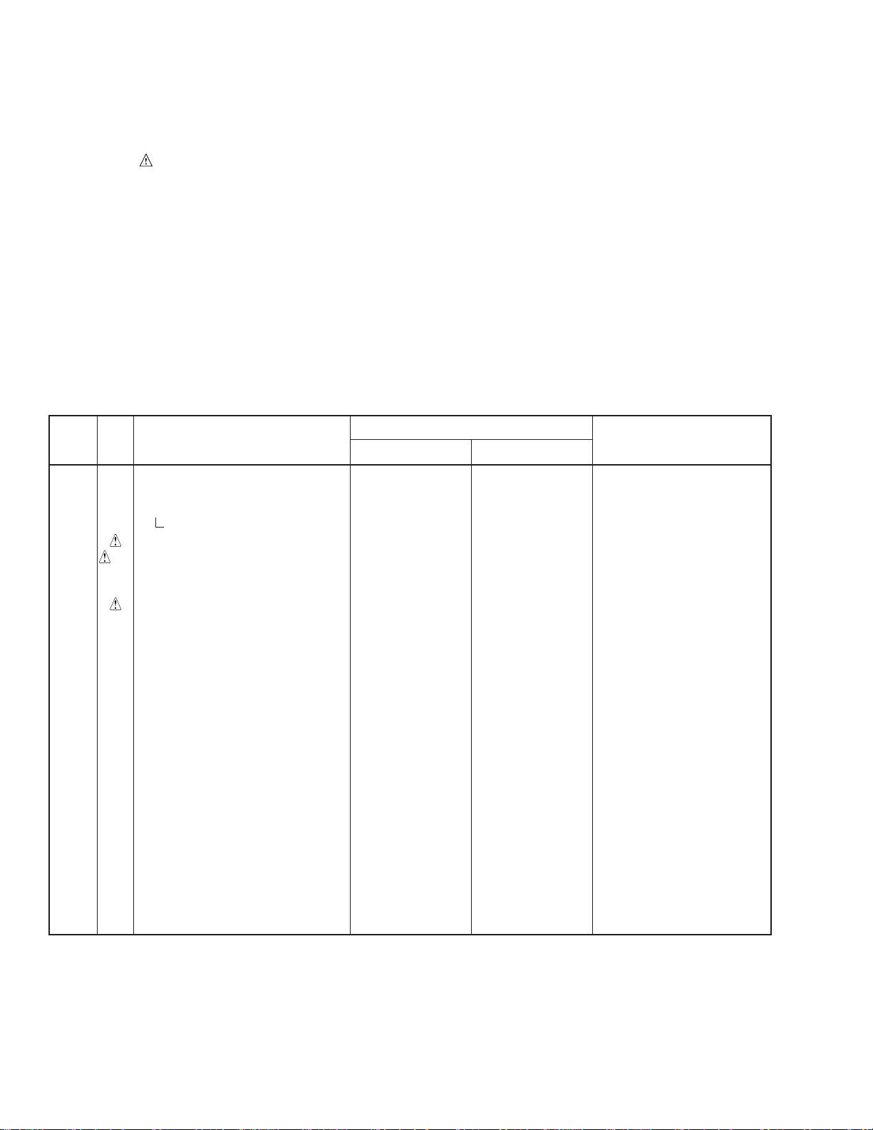
7 CONTRAST TABLE
DV-3300/RAMXQ and DV-333/KUXQ are constructed the same except for the following:
Ref.
Mark Symbol and Description
No.
1
= 561................................................... RD1/4PU 5 6 1 J
3
= 473 .................................................. RD1/4PU 4 7 3 J
Part No.
DV-333/KUXQ DV-3300/RAMXQ
Remarks
PCB ASSEMBLIES
P5 - 1 DVDM Assy VWS1412 VWS1413
FLJB Assy VWM1991 VWM2051
P5 - 4 FLJB Assy VWV1748 VWV1782
P5 - 5 POWER SUPPLY Unit VWR1327 VWR1330 (∗1)
P5 - 5
P3 - 1 Power Cord ADG7022 ADG7018
P3 - 9 Packing Case VHG1903 VHG1935
P3 -11 NSP Warranty Card ARY7045 ARY7046
P3 -13 Operating Instructions (English) VRB1244 Not used
P3 -13 Operating Instructions (Simp-Chinese) Not used VRC1113
P5 -12 Rear Panel VNA2174 VNA2196
P5 -13 Tray VNL1858 VNL1884
P5 -15 Pioneer Name Plate VAM1099 VAM1100
P5 -16 Tray Panel VNK4591 VNK4592
P5 -17 Front Panel Assy VXA2407 VXA2406
P5 -18 NSP Label VRW1629 Not used
P5 -19 NSP Pop Label VRW1830 VRW1832
P5 -20 Bonnet S VXX2651 VXX2652
P5 -24 Screw BCZ40P060FZK BCZ40P060FNI
P5 -26 FL Lens VNK4593 VNK4734
NSP
POWER SUPPLY Unit VWR1328 VWR1331 (∗1)
PACKING
EXTERIOR
Label Not used VRW1699 For Bonnet
Label Not used VRW1739 For Rear Panel
• For PCB assemblies, Refer to “CONTRAST OF PCB ASSEMBLIES”, “PCB PARTS LIST”, “2. SCHEMATIC DIAGRAM” and “3. PCB
CONNECTION DIAGRAM”.
∗1 : As for POWER SUPPLY Unit, either VWR1330 or VWR1331 is installed. Install VWR1330 when replacing the POWER SUPPLY Unit.
2

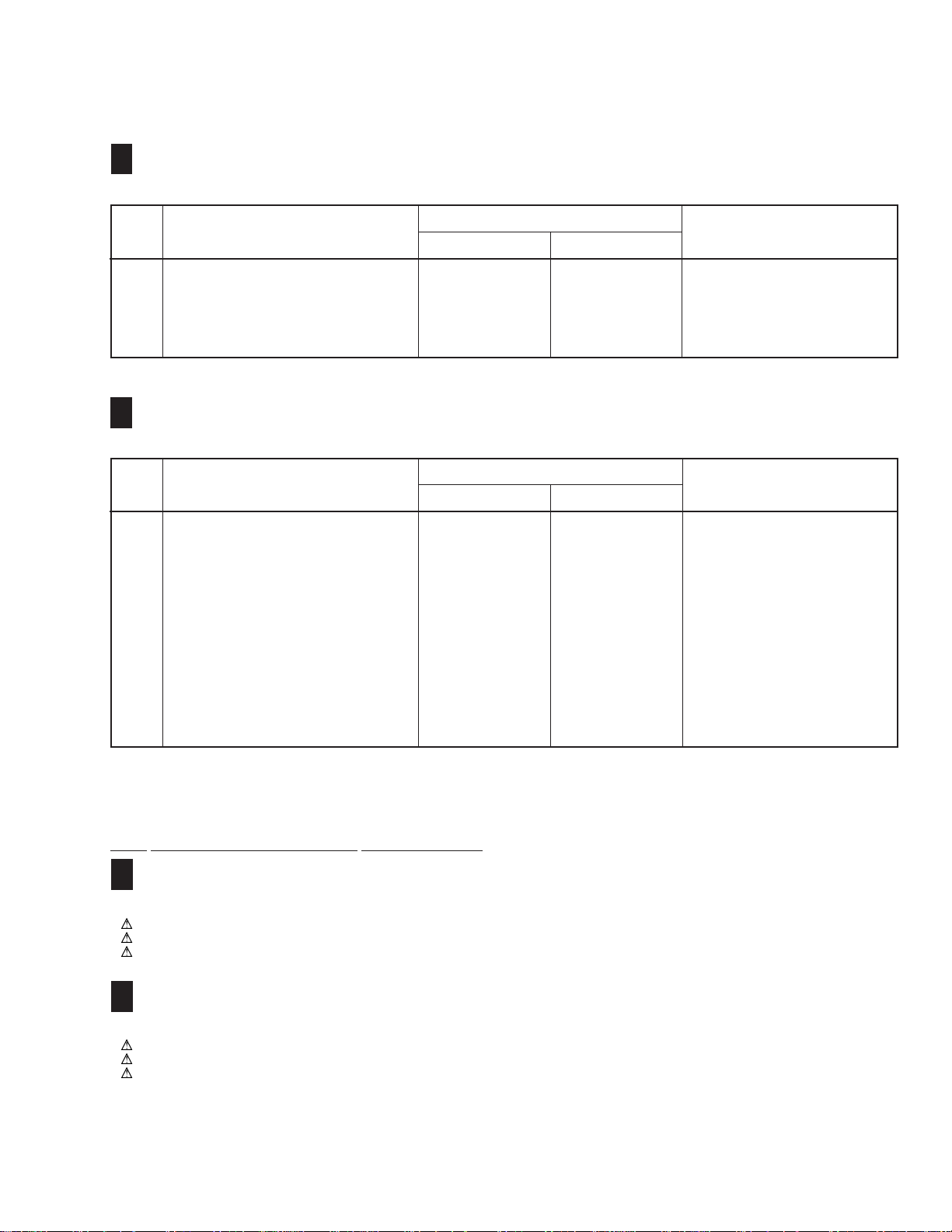
7 CONTRAST OF PCB ASSEMBLIES
D
DVDM ASSY
F
VWS1413 and VWS1412 are constructed the same except for the following:
DV-3300
Mark Symbol and Description
IC13 VYW1727 VYW1700
R1 Not used RS1/16S103J For CHECKER
R2 RS1/16S103J RS1/16S333J For CHECKER
R882 Not used DCN1106 (0Ω)
R951–R955 Not used RS1/16S0R0J
E
FLJB ASSY
F
VWV1782 and VWV1748 are constructed the same except for the following:
Mark Symbol and Description
S401 Not used VSH1020
R118 RS1/10S220J RS1/10S180J
R119 RS1/10S220J RS1/10S330J
R140 RS1/10S0R0J RS1/10S273J
R141 RS1/10S622J RS1/10S163J
R142 Not used RS1/10S683J
R143 RS1/10S363J RS1/10S272J
R486 RS1/10S682J Not used
R487 Not used RS1/10S682J
R488 Not used RS1/10S153J
VWS1412 VWS1413
VWV1748 VWV1782
Part No.
Part No.
Remarks
Remarks
R489 Not used RS1/10S103J
7 PCB PARTS LIST
Mark No. Description Part No.
I
F
POWER SUPPLY UNIT (VWR1330)
OTHERS
P101 PROTECTOR (800mA) AEK7063
P102 PROTECTOR (1.6A) AEK7066
FU101 FUSE (2.5A) REK1102
I
POWER SUPPLY UNIT (VWR1331)
F
OTHERS
P101 PROTECTOR (630mA) VZE1001
P102 PROTECTOR (1.25A) VZE1003
P103 PROTECTOR (1.6A) VZE1004
Note : When the fuse(F001) on VWR1331 blow out, VWR1331 might
be damaged.
At that time, exchange VWR1331 for VWR1330.
3

1
23
DV-3300
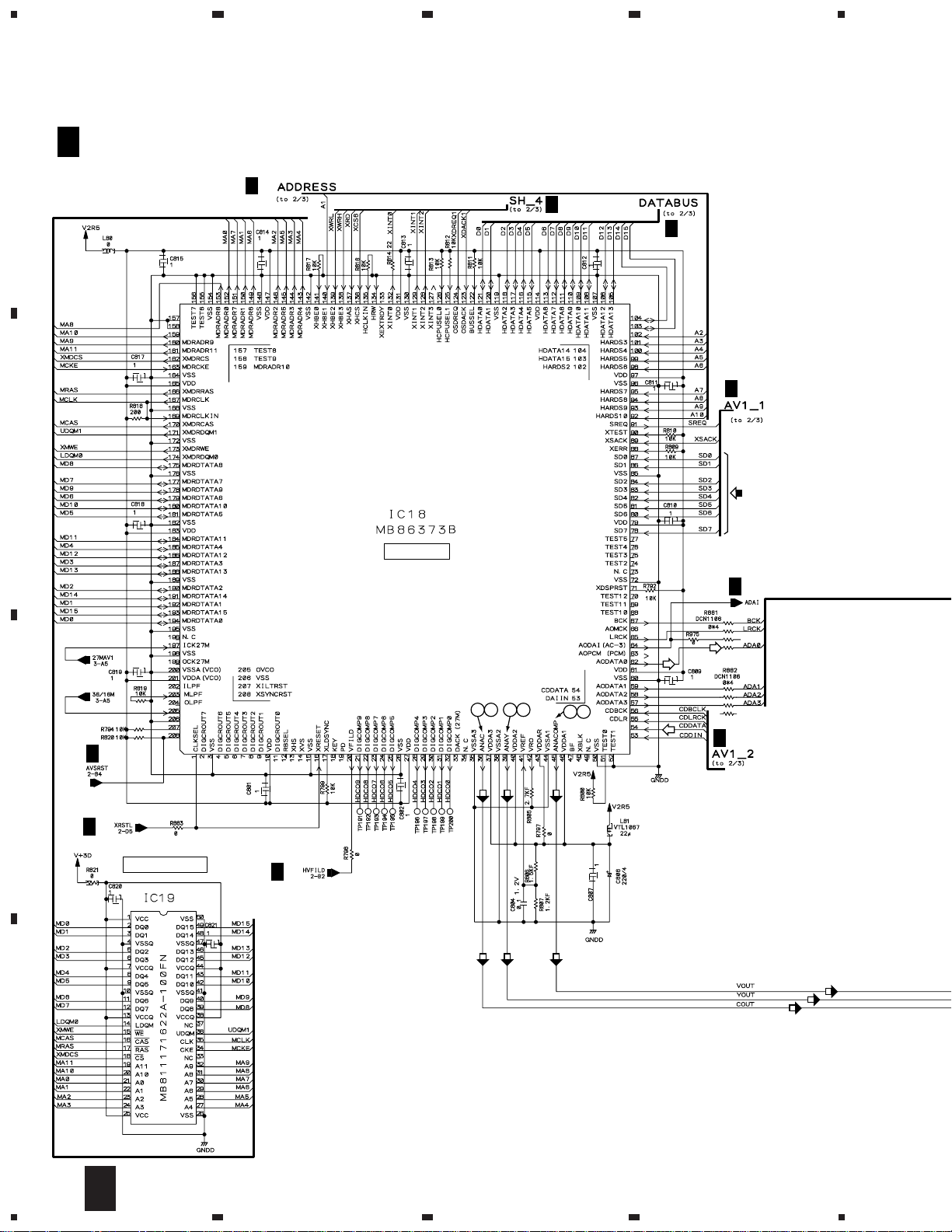
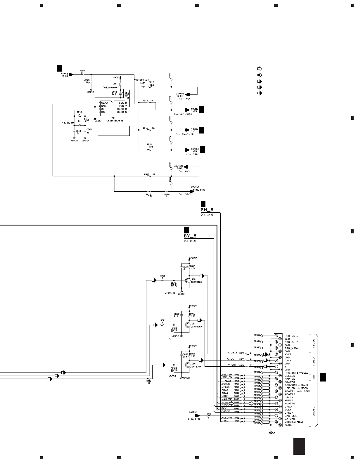
2. SCHEMATIC DIAGRAM
2.1 DVDM ASSY (3/3)
4
A
D 3/3F
B
DVDM ASSY (VWS1413)
D
2/3
AV-1
D
2/3
D
2/3
D
2/3
D
2/3
1417
1316
D
C
D
2/3
D
2/3
16M SDRAM
(Y)
(C)
D
2/3
(Y)
(C)
(VCB)
(VCB)
1215
D
2/3
(VCB)
(Y)
(C)
4
3/3F
D
1234

5
678
DV-3300
Note : When ordering service parts, be sure to refer to "EXPLODED VIEWS and PARTS LIST" or "PCB PARTS LIST".
D
2/3
D
2/3
: AUDIO SIGNAL ROUTE
: ROM DATA SIGNAL ROUTE
(VCB)
: V/CB SIGNAL ROUTE
(Y)
: Y SIGNAL ROUTE
(C)
: C SIGNAL ROUTE
A
CLOCK
GENERATOR
(VCB)
D
2/3
D
1/3
B
D
2/3
D
2/3
(VCB)
C
(Y)
(C)
(VCB)
(Y)
(C)
(Y)
(VCB)
(C) (C)
CN15
VKN1763
(Y)
E 3/3F
CN106
D
3/3F
D
5
6
7
8
5
 Loading...