

Page 1
PIONEER CORPORATION 4-1, Meguro 1-chome, Meguro-ku, Tokyo 153-8654, Japan
PIONEER ELECTRONICS (USA) INC. P.O. Box 1760, Long Beach, CA 90801-1760, U.S.A.
PIONEER EUROPE NV Haven 1087, Keetberglaan 1, 9120 Melsele, Belgium
PIONEER ELECTRONICS ASIACENTRE PTE. LTD. 253 Alexandra Road, #04-01, Singapore 159936
PIONEER CORPORATION 2006
POWE R
PROFESSIONAL MIXER
MIC
MIC 1MIC 2
-
12
-
12
MIC
OFF ON
HARMONIC
SOUND COLOR FX
CRUSH
FADER START
1234
HEADPHONES
MONO SPLIT STEREO
MIXING
LEVEL
PHONES
MIC 1
LEVEL
0
MIC 2
LEVEL
0
HI
+
6
EQ
LOW
+
6
TALK
OVER
SWEEP
FILTER
MASTERCUE
0
/DIGITAL PHONOCD/DIGITAL PHON O
CD
LINE
TRIM
TRIM
OVER
OVER
10
10
+
9
+
9
7
7
HI
HI
4
4
2
2
1
1
0
0
+6-
26
+6-
26
MID
MID
–1
–1
–2
–2
EQ EQ EQ EQ
–3
–3
–5
–5
+
6
-
26
+6-
26
–7
–7
LOW
LOW
–10
–10
–15
–15
–24
–24
dB dB dB dB
+6-
26
+6-
26
COLOR
COLOR
LOW
LOW
HI
HI
CUE
CUE
10
9
8
7
6
5
4
3
2
1
0
CROSS FADER ASSIGN
A B
LINE
/DIGITAL PHONO
/DIGITAL
TRIM
OVER
10
+
9
7
HI
4
2
1
0
+6-
26
MID
–1
–2
–3
–5
+6-
26
–7
LOW
–10
–15
–24
+6-
26
COLOR
LOW
HI
CUE
10
10
9
9
8
8
7
7
6
6
5
5
4
4
3
3
2
2
1
1
0
0
A THRU BA THRU BA THRU B
LINE
OVER
10
7
4
2
1
0
26
–1
–2
–3
–5
26
–7
–10
–15
–24
26
LOW
A THRU B
TRIM
+
9
HI
+6-
MID
+6-
LOW
+6-
COLOR
HI
CUE CUE
BOOTH MONITO R
CROSS FADER
MASTER
LR
BALANCE
MONO STEREO
CH FADER
LEVEL
0
OVER
10
7
4
2
1
0
–1
–2
–3
–5
–7
–10
BEAT
–15
–24
MIDI START
/STOP
AUTO/ TAP
dB
TAP
RL
CUE
BEAT EFFECTS
PHASER
FLANGER
FILTER
REVERB
TRANS
ROBOT
PAN
CHORUS
REV DLY
ROLL
ECHO
REV ROLL
DELAY
SND/RTN
MIC
4
3
CF.A
2
CF.B
1
MASTER
0
TIME
LEVEL/DEPTH
MAX
MIN
ON/OFF
ORDER NO.
RRV3340
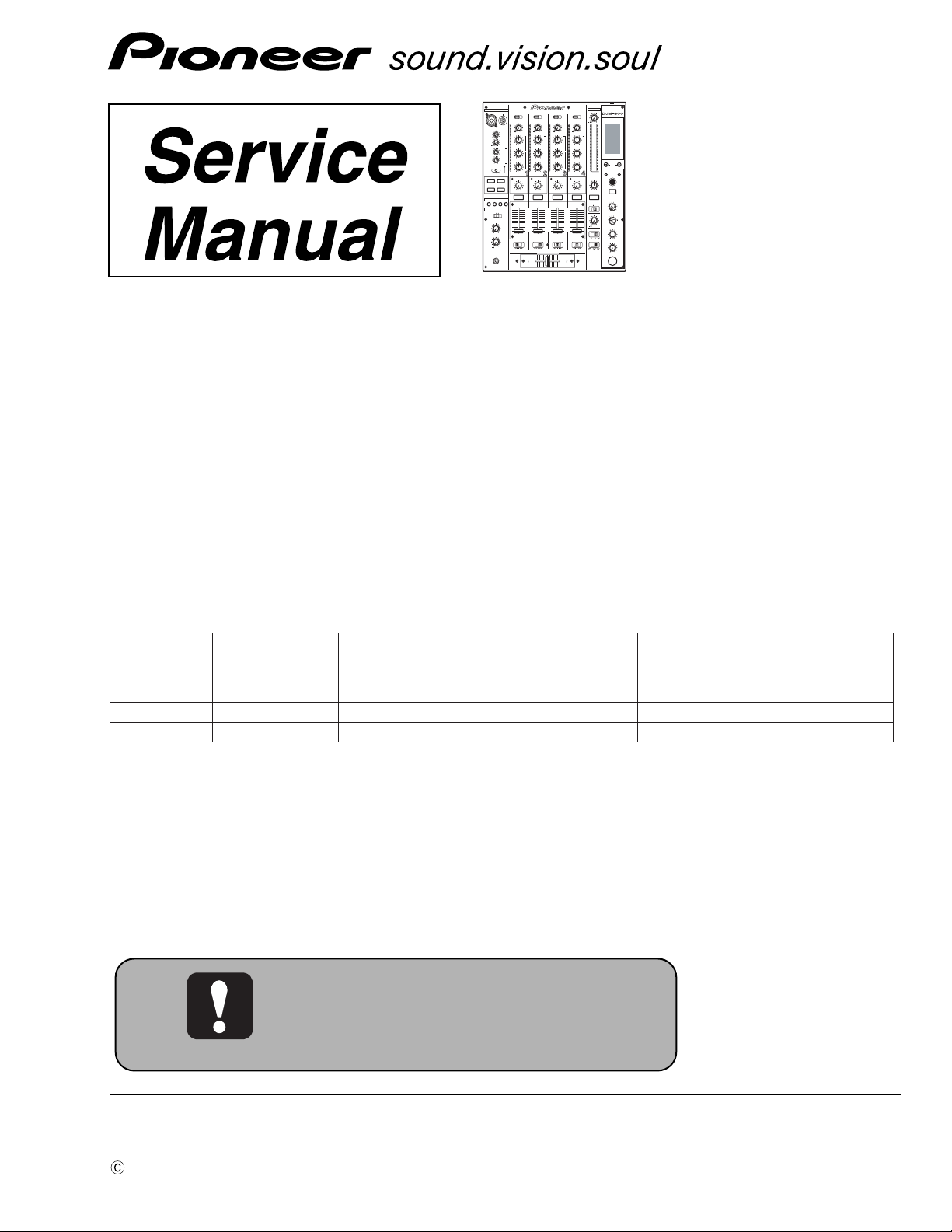
DJM-800
DJ MIXER
DJM-800
ROTARY VOLUME KIT
DJC-800RV
THIS MANUAL IS APPLICABLE TO THE FOLLOWING MODEL(S) AND TYPE(S).
Model Type Power Requirement Remarks
DJM-800 KUCXJ AC120V
DJM-800 WYXJ5 AC220 - 240V
DJM-800 TLXJ AC110 - 120V / 220 - 240V
DJC-800RV ZXJ/WL5 —
For details, refer to "Important Check Points for good servicing".
T-IZR MAR. 2006 printed in Japan
Page 2
1234
SAFETY INFORMATION
A
This service manual is intended for qualified service technicians ; it is not meant for the casual do-ityourselfer. Qualified technicians have the necessary test equipment and tools, and have been trained
to properly and safely repair complex products such as those covered by this manual.
Improperly performed repairs can adversely affect the safety and reliability of the product and may
void the warranty. If you are not qualified to perform the repair of this product properly and safely, you
should not risk trying to do so and refer the repair to a qualified service technician.
WARNING
This product contains lead in solder and certain electrical parts contain chemicals which are known to the state of California to
causecancer, birth defects or other reproductive harm.
B
NOTICE
(FOR CANADIAN MODEL ONLY)
Fuse symbols (fast operating fuse) and/or (slow operating fuse) on PCB indicate that replacement
parts must be of identical designation.
Health & Safety Code Section 25249.6 – Proposition 65
REMARQUE
(POUR MODÈLE CANADIEN SEULEMENT)
Les symboles de fusible (fusible de type rapide) et/ou (fusible de type lent) sur CCI indiquent que
les pièces de remplacement doivent avoir la même désignation.
C
(FOR USA MODEL ONLY)
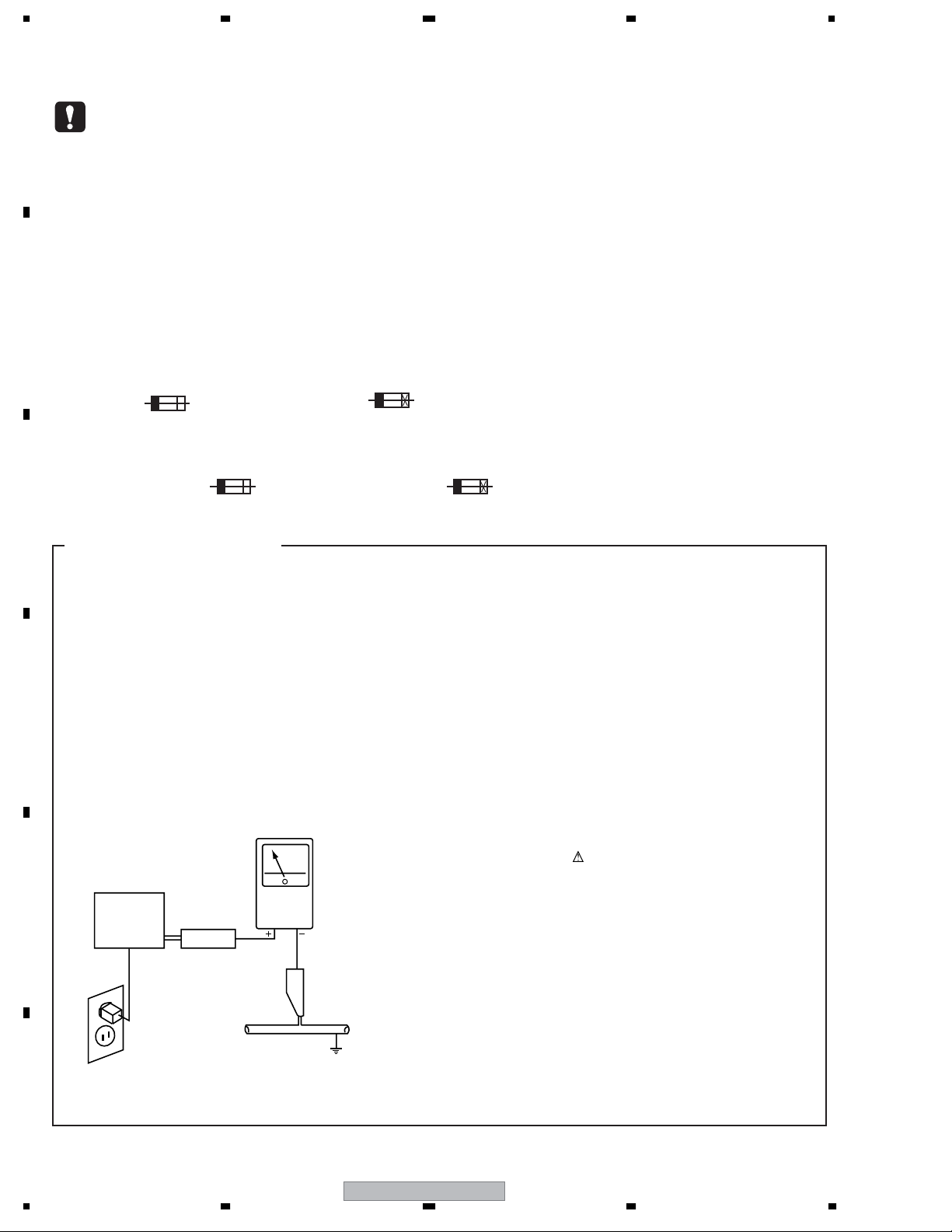
1. SAFETY PRECAUTIONS
The following check should be performed for the
continued protection of the customer and
service technician.
LEAKAGE CURRENT CHECK
Measure leakage current to a known earth ground (waterpipe
D
E
, conduit, etc.) by connecting a leakage current tester
such as Simpson Model 229-2 or equivalent between the
earth ground and all exposed metal parts of the appliance
(input/output terminals, screwheads, metal overlays, control
shaft, etc.). Plug the AC line cord of the appliance directly
into a 120V AC 60Hz outlet and turn the AC power switch
on. Any current measured must not exceed 0.5mA.
Reading should
not be above
0.5mA
Device
under
test
Test all
exposed metal
surfaces
Also test with
plug reversed
(Using AC adapter
plug as required)
Leakage
current
tester
Earth
ground
ANY MEASUREMENTS NOT WITHIN THE LIMITS
OUTLINED ABOVE ARE INDICATIVE OF A POTENTIAL
SHOCK HAZARD AND MUST BE CORRECTED BEFORE
RETURNING THE APPLIANCE TO THE CUSTOMER.
2. PRODUCT SAFETY NOTICE
Many electrical and mechanical parts in the appliance
have special safety related characteristics. These are
often not evident from visual inspection nor the protection
afforded by them necessarily can be obtained by using
replacement components rated for voltage, wattage, etc.
Replacement parts which have these special safety
characteristics are identified in this Service Manual.
Electrical components having such features are identified
by marking with a on the schematics and on the parts list
in this Service Manual.
The use of a substitute replacement component which does
not have the same safety characteristics as the PIONEER
recommended replacement one, shown in the parts list in
this Service Manual, may create shock, fire, or other hazards.
Product Safety is continuously under review and new
instructions are issued from time to time. For the latest
information, always consult the current PIONEER Service
Manual. A subscription to, or additional copies of, PIONEER
Service Manual may be obtained at a nominal charge
from PIONEER.
F
2
1234
AC Leakage Test
DJM-800
Page 3
5678
[Important Check Points for Good Servicing]
In this manual, procedures that must be performed during repairs are marked with the below symbol.
Please be sure to confirm and follow these procedures.
1. Product safety
Please conform to product regulations (such as safety and radiation regulations), and maintain a safe servicing environment by
following the safety instructions described in this manual.
1 Use specified parts for repair.
Use genuine parts. Be sure to use important parts for safety.
2 Do not perform modifications without proper instructions.
Please follow the specified safety methods when modification(addition/change of parts) is required due to interferences such as
radio/TV interference and foreign noise.
3 Make sure the soldering of repaired locations is properly performed.
When you solder while repairing, please be sure that there are no cold solder and other debris.
Soldering should be finished with the proper quantity. (Refer to the example)
4 Make sure the screws are tightly fastened.
Please be sure that all screws are fastened, and that there are no loose screws.
5 Make sure each connectors are correctly inserted.
Please be sure that all connectors are inserted, and that there are no imperfect insertion.
6 Make sure the wiring cables are set to their original state.
Please replace the wiring and cables to the original state after repairs.
In addition, be sure that there are no pinched wires, etc.
7 Make sure screws and soldering scraps do not remain inside the product.
Please check that neither solder debris nor screws remain inside the product.
8 There should be no semi-broken wires, scratches, melting, etc. on the coating of the power cord.
Damaged power cords may lead to fire accidents, so please be sure that there are no damages.
If you find a damaged power cord, please exchange it with a suitable one.
9 There should be no spark traces or similar marks on the power plug.
When spark traces or similar marks are found on the power supply plug, please check the connection and advise on secure
connections and suitable usage. Please exchange the power cord if necessary.
0 Safe environment should be secured during servicing.
When you perform repairs, please pay attention to static electricity, furniture, household articles, etc. in order to prevent injuries.
Please pay attention to your surroundings and repair safely.
A
B
C
D
2. Adjustments
To keep the original performance of the products, optimum adjustments and confirmation of characteristics within specification.
Adjustments should be performed in accordance with the procedures/instructions described in this manual.
3. Lubricants, Glues, and Replacement parts
Use grease and adhesives that are equal to the specified substance.
Make sure the proper amount is applied.
4. Cleaning
For parts that require cleaning, such as optical pickups, tape deck heads, lenses and mirrors used in projection monitors, proper
cleaning should be performed to restore their performances.
5. Shipping mode and Shipping screws
To protect products from damages or failures during transit, the shipping mode should be set or the shipping screws should be
installed before shipment. Please be sure to follow this method especially if it is specified in this manual.
56
DJM-800
E
F
3
7
8
Page 4

1234
CONTENTS
1. SPECIFICATIONS ............................................................................................................................................ 5
2. EXPLODED VIEWS AND PARTS LIST ............................................................................................................6
A
B
C
D
E
F
2.1 PACKING SECTION .................................................................................................................................. 6
2.2 EXTERIOR SECTION................................................................................................................................ 8
2.3 CONTROL PANEL SECTION .................................................................................................................. 10
3. BLOCK DIAGRAM AND SCHEMATIC DIAGRAM..........................................................................................12
3.1 OVERALL BLOCK DIAGRAM_1.............................................................................................................. 12
3.2 OVERALL BLOCK DIAGRAM_2.............................................................................................................. 14
3.3 OVERALL WIRING DIAGRAM................................................................................................................. 16
3.4 INPUT ASSY (1/6) ...................................................................................................................................18
3.5 INPUT ASSY (2/6) ...................................................................................................................................20
3.6 INPUT ASSY (3/6) ...................................................................................................................................22
3.7 INPUT ASSY (4/6) ...................................................................................................................................24
3.8 INPUT ASSY (5/6) ...................................................................................................................................26
3.9 INPUT ASSY (6/6) ...................................................................................................................................28
3.10 MIC 1 ASSY........................................................................................................................................... 30
3.11 PANEL 1 ASSY...................................................................................................................................... 32
3.12 TRIM1 to TRIM 4 ASSYS....................................................................................................................... 36
3.13 MAIC 2 ASSY ........................................................................................................................................ 37
3.14 PANEL 2 ASSY...................................................................................................................................... 38
3.15 CHFD 1 to CHFD 4 and CRSFD ASSYS............................................................................................... 40
3.16 DIGIA ASSY........................................................................................................................................... 41
3.17 DSP ASSY (1/3)..................................................................................................................................... 42
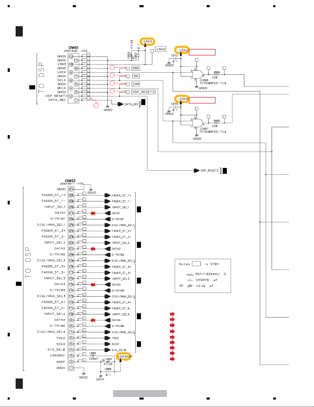
3.18 DSP ASSY (2/3)..................................................................................................................................... 46
3.19 DSP ASSY (3/3)..................................................................................................................................... 50
3.20 OUTPUT ASSY (1/3) .............................................................................................................................54
3.21 OUTPUT ASSY (2/3) .............................................................................................................................56
3.22 OUTPUT ASSY (3/3) .............................................................................................................................58
3.23 DIGIC ASSY .......................................................................................................................................... 60
3.24 DIGIB ASSY........................................................................................................................................... 64
3.25 HPAMP ASSY........................................................................................................................................ 66
3.26
HPJACK
ACSW
3.27
3.28 SW POWER SUPPLY UNIT................................................................................................................... 70
3.29 VOLTAGES............................................................................................................................................. 72
3.30 WAVEFORMS........................................................................................................................................ 78
4. PCB CONNECTION DIAGRAM ..................................................................................................................... 84
4.1 INPUT ASSY............................................................................................................................................ 84
4.2 PANEL 1 ASSY........................................................................................................................................ 88
4.3 TRIM 1 to TRIM 4 and ACSW ASSYS..................................................................................................... 92
4.4 MIC1 and MIC2 ASSYS........................................................................................................................... 94
4.5 CHFD1, CHFD2, CHFD3 and CHFD4 ASSYS ........................................................................................ 95
4.6 PANEL 2 and DIGIA ASSYS.................................................................................................................... 96
4.7 DSP ASSY ............................................................................................................................................. 100
4.8 OUTPUT ASSY...................................................................................................................................... 104
4.9 CRSFD, DIGIC and SLSW ASSYS........................................................................................................ 108
4.10 DIGIB ASSY......................................................................................................................................... 112
4.11 HPAMP and HPJACK ASSYS.............................................................................................................. 114
5. PCB PARTS LIST ......................................................................................................................................... 116
6. ADJUSTMENT ............................................................................................................................................. 123
7. GENARAL INFORMATION........................................................................................................................... 124
7.1 DIAGNOSIS ........................................................................................................................................... 124
7.1.1 TEST MODE .................................................................................................................................... 124
7.1.2 REWRITING THE FIRMWARE........................................................................................................ 133
7.2 POWER ON SEQUENCE...................................................................................................................... 146
7.3 DISASSEMBLY ...................................................................................................................................... 147
7.4 IC INFORMATION.................................................................................................................................. 152
8. PANEL FACILITES ....................................................................................................................................... 167
9. ROTARY VOLUME KIT (DJC-800RV)........................................................................................................... 172
9.1 PACKING SECTION .............................................................................................................................. 172
9.2 EXTERIOR SECTION............................................................................................................................ 173
9.3 SCHEMATIC DIAGAM........................................................................................................................... 174
9.4 DISASSEMBLY ...................................................................................................................................... 175
ASSYS .................................................................................................................................... 68
ASSY.......................................................................................................................................... 69
4
1234
DJM-800
Page 5
5678
1. SPECIFICATIONS
SPECIFICATIONS
1. General
Power source (/KUCXJ) .............................................. AC 120 V, 60 Hz
Power source (/WYXJ5) ..................................... AC 220–240V, 50/60 Hz
Power source (/TLXJ) ......................... AC 110–120/220–240V, 50/60 Hz
Power consumption ..................................................................... 32W
Operating temperature ..................... +5 ˚C to +35 ˚C (+41 ˚F to +95 ˚F)
Operating humidity ....................5 % to 85 % (without condensation)
Weight ..........................................................................8.0 kg (16.54 lb )
Maximum dimensions ...................... 320 (W) x 381 (D) x 108 (H) mm
2. Audio section
Sampling rate .............................................................................96 kHz
A/D, D/A converter ...................................................................... 24 bits
Frequency response
LINE ......................................................................... 20 Hz to 20 kHz
MIC .......................................................................... 20 Hz to 20 kHz
PHONO ......................................................... 20 Hz to 20 kHz (RIAA)
S/N ratio (at rated output)
LINE ....................................................................................... 105 dB
PHONO .................................................................................... 88 dB
MIC .......................................................................................... 84 dB
Distortion (LINE-MASTER 1) .................................................... 0.005 %
Standard input level/Input impedance
PHONO 2 to 4 ............................................................ –52 dBu/47 kΩ
MIC 1, MIC 2 ............................................................... –52 dBu/3 kΩ
LINE, LINE/CD 1 to 4 ................................................. –12 dBu/22 kΩ
RETURN .................................................................... –12 dBu/22 kΩ
Standard output level/Load impedance/Output impedance
MASTER 1 ..............................................
MASTER 2 .......................................................... +2 dBu/10 k Ω/1 kΩ
REC ..................................................................... –8 dBu/10 kΩ /1 kΩ
BOOTH ............................................................. +2 dBu/600Ω /600Ω
SEND ................................................................ –12dBu/10 kΩ /1 kΩ
PHONES ................................................ +8.5 dBu/32Ω /22Ω or less
Rated output level/Load impedance
MASTER 1 ................................................................ +22 dBu/10kΩ
MASTER 2 ................................................................. +20 dBu/10 kΩ
Crosstalk (LINE) ............................................................................ 88 dB
Channel equalizer response
HI ............................................................... –26 dB to +6 dB (13 kHz)
MID ............................................................. –26 dB to +6 dB (1 kHz)
LOW ............................................................ –26 dB to +6 dB (70 Hz )
Microphone equalizer response
HI ............................................................... –12 dB to +6 dB (10 kHz)
LOW .......................................................... –12 dB to +6 dB (100 Hz )
12-5/8 (W) x 15 (D) x 4-1/4 (H) in
+2 dBu/10kΩ /10Ω or less
3. Input/output connector systems
PHONO input connectors
RCA pin jacks .................................................................................. 3
LINE/CD input connectors
RCA pin jacks .................................................................................. 4
LINE input connectors
RCA pin jacks .................................................................................. 1
MIC input connectors
XLR connector/phone jack (Ø6.3 mm) ...........................................1
Phone jack (Ø6.3 mm) ....................................................................1
DIGITAL coaxial input connectors
RCA pin jacks .................................................................................. 4
RETURN input connectors
Phone jacks (Ø6.3 mm) .................................................................. 1
MASTER output connectors
XLR connectors ...............................................................................1
RCA pin jacks .................................................................................. 1
BOOTH output connectors
Phone jacks (Ø6.3 mm) .................................................................. 1
REC output connectors
RCA pin jacks .................................................................................. 1
SEND output connectors
Phone jacks (Ø6.3 mm) .................................................................. 1
DIGITAL coaxial output connector
RCA pin jack ....................................................................................1
MIDI OUT connector
5P DIN.............................................................................................. 1
PHONES output connector
Stereo phone jack (Ø6.3 mm) ........................................................ 1
CONTROL connector
Mini phone jacks (Ø3.5 mm) ..........................................................4
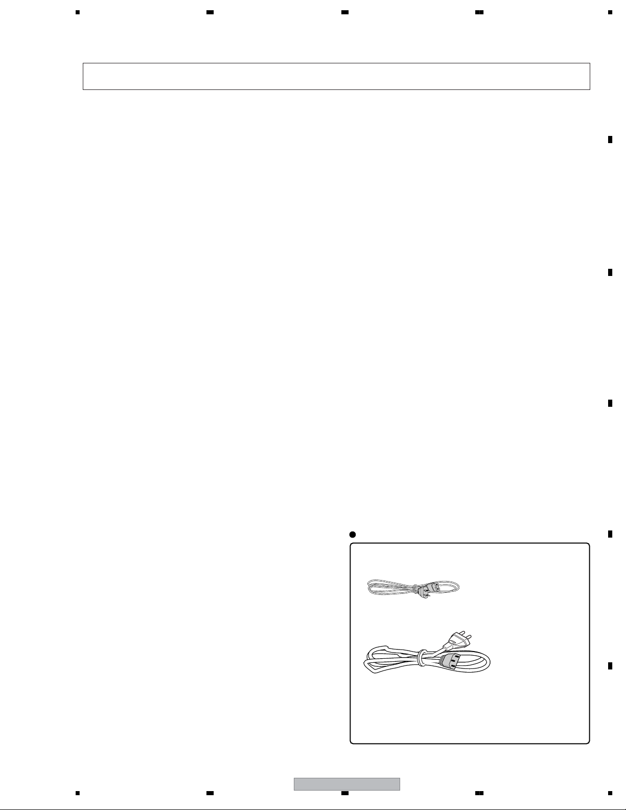
4. Accessories
Operating Instructions .........................................................................1
Power cord ........................................................................................... 1
Warranty card ......................................................................................1
Specifications and appearance are subject to change without notice.
Accessories
Power cord
(KUCXJ : DDG1028)
A
B
C
D
(WYXJ5,TLXJ : ADG7062)
Operating instrucions
Warranty card (KUCXJ only)
DJM-800
56
E
F
5
7
8
Page 6
1234
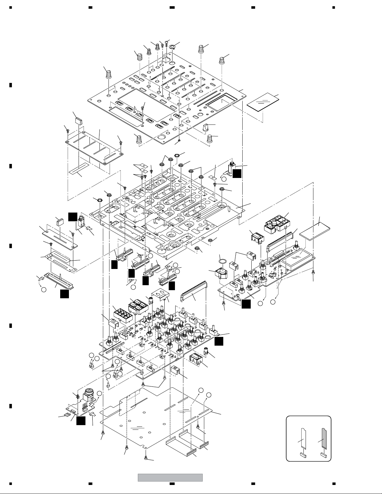
2. EXPLODED VIEWS AND PARTS LIST
NOTES:
A
Parts marked by "NSP" are generally unavailable because they are not in our Master Spare Parts List.
The mark found on some component parts indicates the importance of the safety factor of the part.
Therefore, when replacing, be sure to use parts of identical designation.
Screws adjacent to mark on product are used for disassembly.
For the applying amount of lubricants or glue, follow the instructions in this manual.
(In the case of no amount instructions, apply as you think it appropriate.)
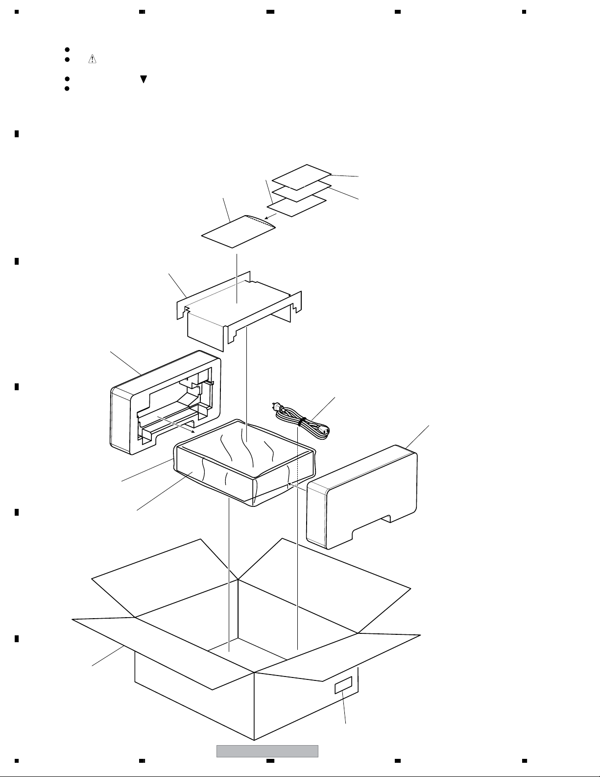
2.1 PACKING SECTION
B
C
5
9
4
12
11
3
D
7
8
2
FRONT
DJM-800
E
6
F
10
6
1234
DJM-800
Page 7
5678
(1) PACKING SECTION PARTS LIST
No. Description Part No.
No. Description Part No.
Mark
1• • • •
2Pad Front DHA1698
3Pad Rear DHA1699
4Pad Top DHA1705
5 Instruction Manual(M800) See Contrast table (2)
6Packing Case See Contrast table (2)
7 Sheet RHX1006
Mark
8 Power Cord See Contrast table (2)
NSP 9 Polyethylene Bag AHG7117
NSP 10 Label See Contrast table (2)
NSP 11 Warranty Card See Contrast table (2)
NSP 12 User Registration Sheet DRM1262
(2) CONTRAST TABLE
DJM-800/WYXJ5, DJM-800/TLXJ and DJM-800/KUCXJ are constructed the same except for the fHollowing
Mark No. Symbol and Description
5 Instruction Manual (English) DRB1393 Not used Not used
5 Instruction Manual (English, French Not used DRB1392 Not used
German, Italian, Dutch, Spanish)
5 Instruction Manual
(English, Spanish, Chinese)
6Packing Case DHG2559 DHG2558 DHG2560
8Power Cord DDG1028 ADG7062 ADG7062
NSP 10 Label DRW2311 VRW1629 VRW1629
NSP 11 Warranty Card ARY7043 Not used Not used
DJM-800
/KUCXJ
Not used Not used DRB1394
DJM-800
/WYXJ5
DJM-800
/TLXJ
A
B
C
>
>
D
E
56
DJM-800
F
7
7
8
Page 8
1234
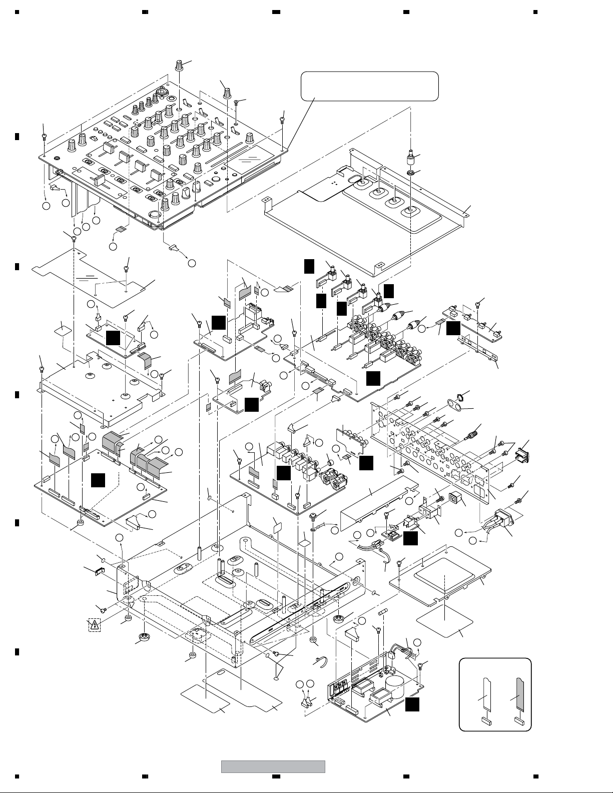
2.2 EXTERIOR SECTION
A
61
51
51
63
Refer to
"2.3 CONTROL PANEL SECTION".
61
50
64
B
C
22
D
59
S
A
O
P
59
Q
M
39
21
P
56
20
42
59
T
24
K
60
29
M
J
11
Q
60
T
R
L
7
J
45
S
12
O
59
31
60
8
B
19
59
K
N
27
16
17
M
O
18
L
J
59
I
16
I
K
47
6
E
A
30
48
47
60
71
I
D
1
33
4/4
23
C
D
5
49
68
3/4
Q
H
4
D
F
9
3
2/4
26
G
L
38
2
A
D
62
D
1/4
15
60
F
R
59
59
15
62
R
59
14
15
67
67
25
59
52
62
N
59
35
59
10
36
66
43
58
62
59
54
62
65
53
G
34
H
28
57
69
E
70
59
40
42
41
42
47
59
47
41
E
59
69
42
D
60
69
C
B
37
44
32
F
55
46
13
Q
NON-CONTACT
SIDE
CONTACT SIDE
8
1234
DJM-800
Page 9
5678
EXTERIOR SECTION PARTS LIST
No. Description Part No.
Mark
1 INPUT Assy DWX2535
2 TRIM 4 Assy DWX2551
3 TRIM 3 Assy DWX2550
4 TRIM 2 Assy DWX2549
5 TRIM 1 Assy DWX2548
6 DSP Assy DWX2534
7 OUTPUT Assy DWX2544
8 DIGIC Assy DWX2547
9 DIGIA Assy DWX2555
10 SLSW Assy DWX2536
11 DIGIB Assy DWX2546
12 HPAMP Assy DWX2556
13 POWER SUPPLY Unit DWR1433
14 ACSW Assy DWX2545
15 Short Pin Plug AKM7008
16 Flexible Cable (31P) DDD1316
17 Flexible Cable (12P) DDD1317
18 Flexible Cable (25P) DDD1318
19 Flexible Cable (16P) DDD1319
20 Flexible Cable (10P) DDD1321
21 Flexible Cable (30P) DDD1322
22 Flexible Cable (25P) DDD1323
23 Flexible Cable (7P) DDD1326
24 Flexible Cable (12P) DDD1327
25 Flexible Cable (6P) DDD1328
26 Flexible Cable (7P) DDD1329
27 Flexible Cable (10P) DDD1333
>
28 AC Inlet Assy See Contrast table (2)
29 Flexible Cable (24P) DDD1330
30 Connector Assy(10P-12P) DKP3763
31 Connector Assy PF05EE-S22
32 Connector Assy PF05EE4S32
33 Connector Assy PF06EE-D12
NSP 34 Rear Panel See Contrast table (2)
35 Bracket TRIM DNF1728
36 Bracket SSW DNF1729
>
>
No. Description Part No.
Mark
37 Shield Case DNH2697
38 Shield Case AC DNH2698
39 Shield Case DSP DNH2699
40 Chassis Assy DXB1881
41 Leg Assy REC-434
NSP 42 Spacer AEB7092
43 PHONE Spacer DEC2914
44 Barrier A DEC2915
45 Styling Sheet DEC2917
46 Bottom Cover DEC2918
47 Blind Label DEC2928
48 Barrier B DEC2944
49 Select Knob (S) DAA1166
50 Extension Shaft DNK4691
51 Rotary SW Knob S DAA1204
52 Bracket PSW DNF1730
53 POWER Knob DAC2306
54 POWER Knob Guard DNK4534
NSP 55 LABEL See Contrast table (2)
56 CAUTION Label DRW2312
57 Blind Cap DNK4218
58 Terminal Screw AKE-031-0
59 Screw BBZ30P060FTB
60 Screw BBZ30P080FTC
61 Screw BCZ30P080FTB
62 Screw BPZ30P080FTB
63 Screw CCZ30P060FTB
64 Flange Nut M7 DBN1011
65 Screw IBZ30P080FTB
66 Nut NKX2FTC
67 Screw PMH30P100FTB
68 Screw PMH40P080FTC
69 Binder (SKB-90BK) ZCA-SKB90BK
NSP 70 Caution LABEL See Contrast table (2)
NSP 71 Earth LABEL See Contrast table (2)
A
B
C
D
(2) CONTRAST TABLE
DJM-800/WYXJ5, /TLXJ and DJM-800/KUCXJ are constructed the same except for the fHollowing :
Mark No. Symbol and Description
28 AC Inlet Assy DKP3761 DKP3762 DKP3762
NSP 34 Rear Panel DNC1800 DNC1789 DNC1791
NSP 55 LABEL DRW2294 DRW2293 DRW2319
NSP 70 Caution LABEL DRW1975 Not used Not used
NSP 71 Earth LABEL DRW2276 Not used Not used
DJM-800
/KUCXJ
DJM-800
56
DJM-800
/WYXJ5
7
DJM-800
/TLXJ
E
F
9
8
Page 10
1234
2.3 CONTROL PANEL SECTION
A
27
33
29
30
54
53
41
28
34
47
54
43
B
C
45
55
20
14
D
54
43
A
P
54
9
H
22
22
58
10
16
36
44
57
56
38
54
5
G
1/4
15
51
39
25
27
6
G
48
21
G
15
E
F
4/4
58
57
17
50
57
56
17
D
7
49
G
8
3/4
2/4
C
57
57
40
31
32
25
E
B
51
57
Dependence
42
23
52
F
35
3
19
4
G
46
37
50
H
24
52
2
C
C
D
E
52
26
11
F
10
1234
B
1
18
52
E
F
A
B
52
52
52
DJM-800
42
13
49
35
G
H
59
52
12
NON-CONTACT
SIDE
CONTACT SIDE
Page 11

5678
CONTROL PANEL SECTION PARTS LIST
No. Description Part No.
Mark
1 MIC 1 Assy DWX2542
2PANEL 1 Assy DWX2552
3 MIC 2 Assy DWX2543
4PANEL 2 Assy DWX2554
5 CHFD 1 Assy DWX2537
6 CHFD 2 Assy DWX2538
7 CHFD 3 Assy DWX2539
8 CHFD 4 Assy DWX2540
9 CRSFD Assy DWX2541
10 HP JACK Assy DWX2553
No. Description Part No.
Mark
50 LEVEL Meter Assy DXB1882
51 Screw AMZ26P040FTC
52 Screw BBZ30P060FTB
53 Screw BPZ30P120FTB
54 Screw CCZ30P060FTB
55 Screw DBA1262
56 Screw DBA1298
57 Flange Nut M9 DBN1008
58 Nut NKX2FTC
A
11 Flexible Cable (12P) DDD1320
12 Flexible Cable (27P) DDD1324
13 Flexible Cable (30P) DDD1325
14 Housing Wire Assy PF03PP-D12
15 Housing Wire Assy PF04PP-D05
16 Housing Wire Assy PF04PP-D20
17 Housing Wire Assy PF04PP4D05
18 Housing Wire Assy PF05FF-D25
NSP 19 Panel Stay DND1254
20 CRF Stay DNF1726
21 MIC Stay DNF1727
22 Fader Packing DEC2903
23 SW Packing DEC2929
24 Barrier (FL) DEC2943
25 SW Packing DED1177
NSP 26 PC Support VEC1508
27 Rotary SW Knob (A) DAA1175
28 Rotary SW Knob (B) DAA1176
29 Rotary SW Knob S (A) DAA1177
30 Rotary SW Knob S (B) DAA1178
B
C
D
31 Select Knob DAA1205
32 Rotary SW Knob (C) DAA1180
33 Rotary SW Knob (HM) DAA1197
34 Rotary SW Knob (MA) DAA1198
35 CUE Knob DAC2215
36 Slide SW Cap (A) DAC2219
37 SET Knob (TAP) DAC2300
38 SET Knob (FS) DAC2301
39 SET Knob (HM) DAC2302
40 EFFECT Knob DAC2304
41 MIC Cap DAC2309
42 Slide SW Cap DAC2310
43 Slider Knob (L2) DAC2371
44 CHF Panel DAH2426
45 CRF Panel DAH2427
46 Disply Panel DAH2428
47 Control Panel DNB1144
48 LENS DNK4532
49 LENS Holder DNK4533
56
DJM-800
E
F
11
7
8
Page 12
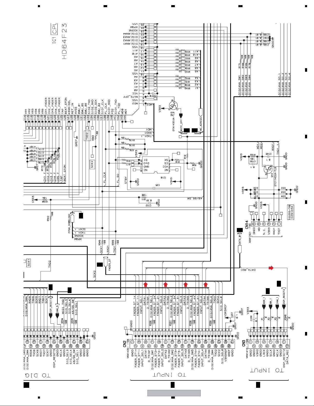
1234
S
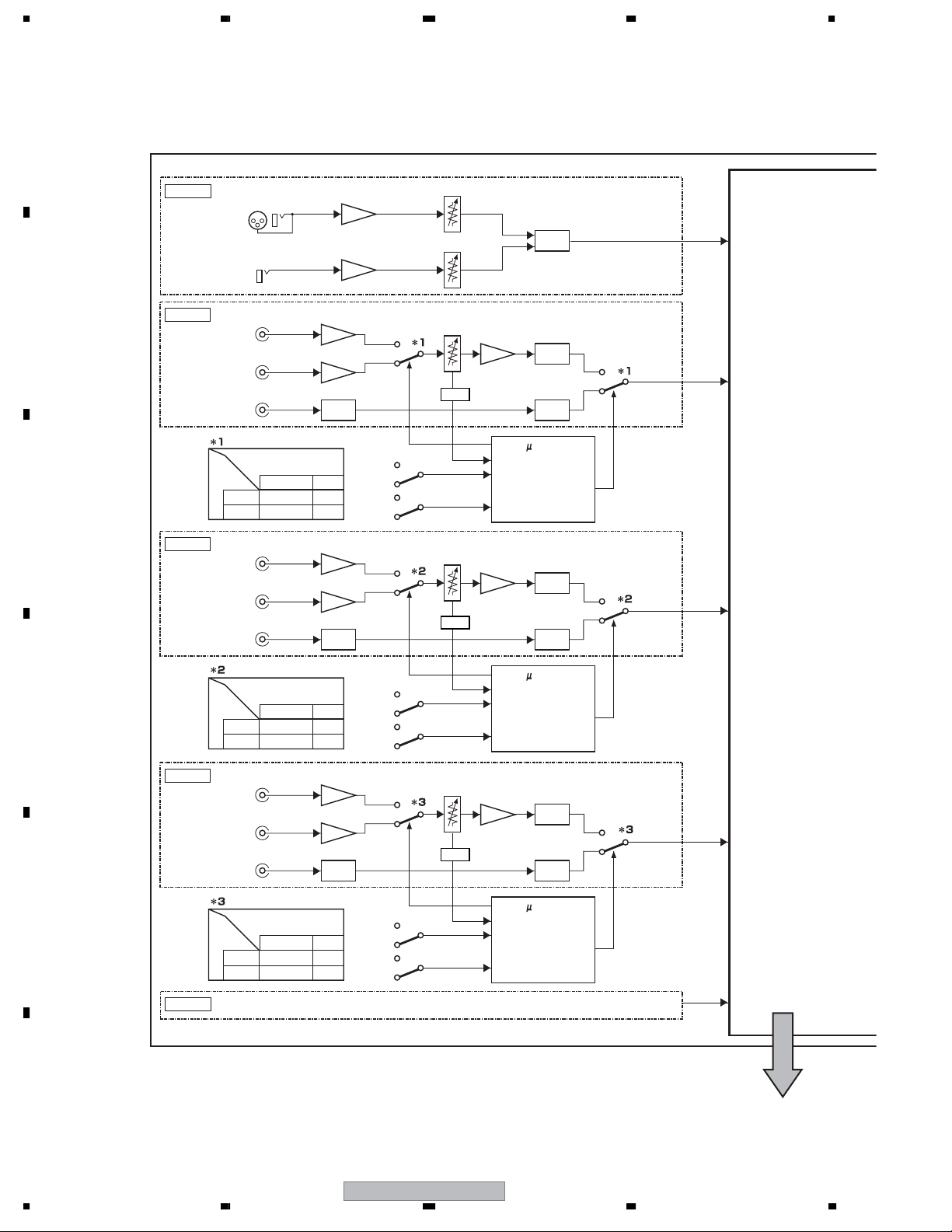
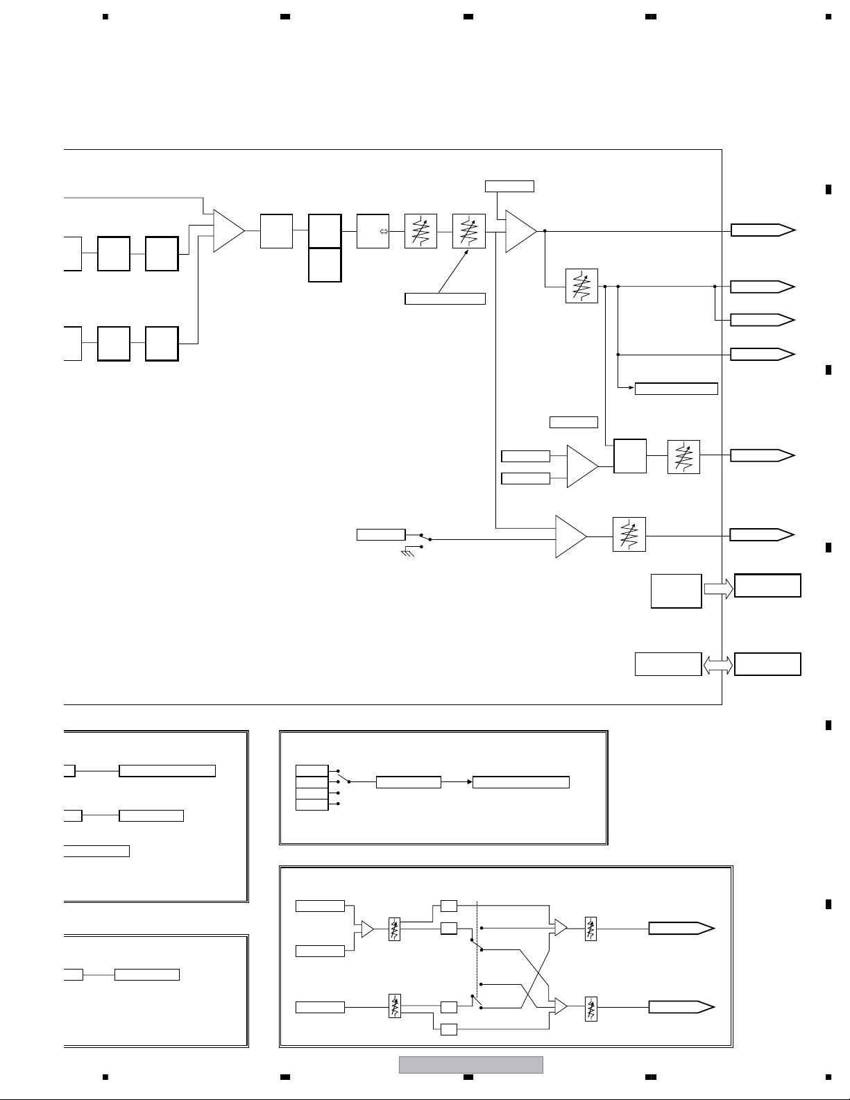
3. BLOCK DIAGRAM AND SCHEMATIC DIAGRAM
3.1 OVERALL BLOCK DIAGRAM_1
A
B
C
BLOCK DIAGRAM
MI C
MIC 1
MIC 2
CH 1
LINE
CD
DIGITAL
CD/DIGITAL
SW .
CD
DIGITAL/CD
CH 2
PHONO
CD
DIGITAL
DIGITAL
DIGITAL
CD/DIGITAL
LINE SW.
CD
PHONO AMP.
MIC AMP
MIC AMP
BUFFER
BUFFER
DIR
LINE
LINE
LINE
BUFFER
DIR
LINE
CD
CD
DIGITAL
MIC 1 LEVEL
MIC 2 LEVEL
TRIM
AD
MATRIX
55
119
MATRIX
19
TRIM
AD
MATRIX
A/D
BUFFER
A/D
SRC
-COM
VR AD
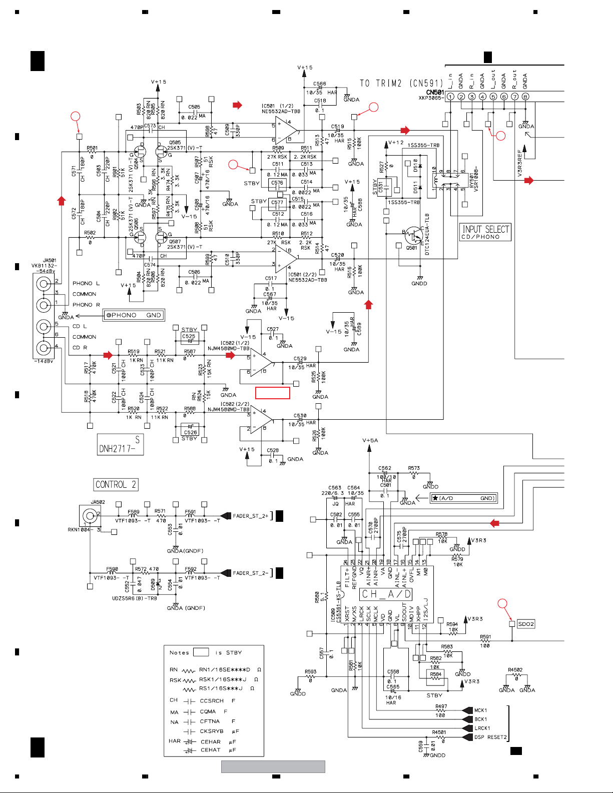
PHONO/LINE SW .
DIGIT AL SEL.
DIGITAL
/ANALOG SW.
BUFFER
A/D
SRC
28
147
143
144
MIC 1
MIC 2
CH 1
CH 2
D
59
CD/DIGI TAL
PHONO SW.
D
CH 3
PHONO
LINE
DIGITAL
SW .
CD
DIGITAL/CD
DIGITAL
CD/DIGI TAL
CD
DIGITAL
PHONO
PHONO
PHONO
PHONO
DIGITAL
PHONO AMP.
BUFFER
DIR
CD
CD
MATRIX
TRIM
119
20
BUFFER
AD
MATRIX
60
E
SW .
LINE
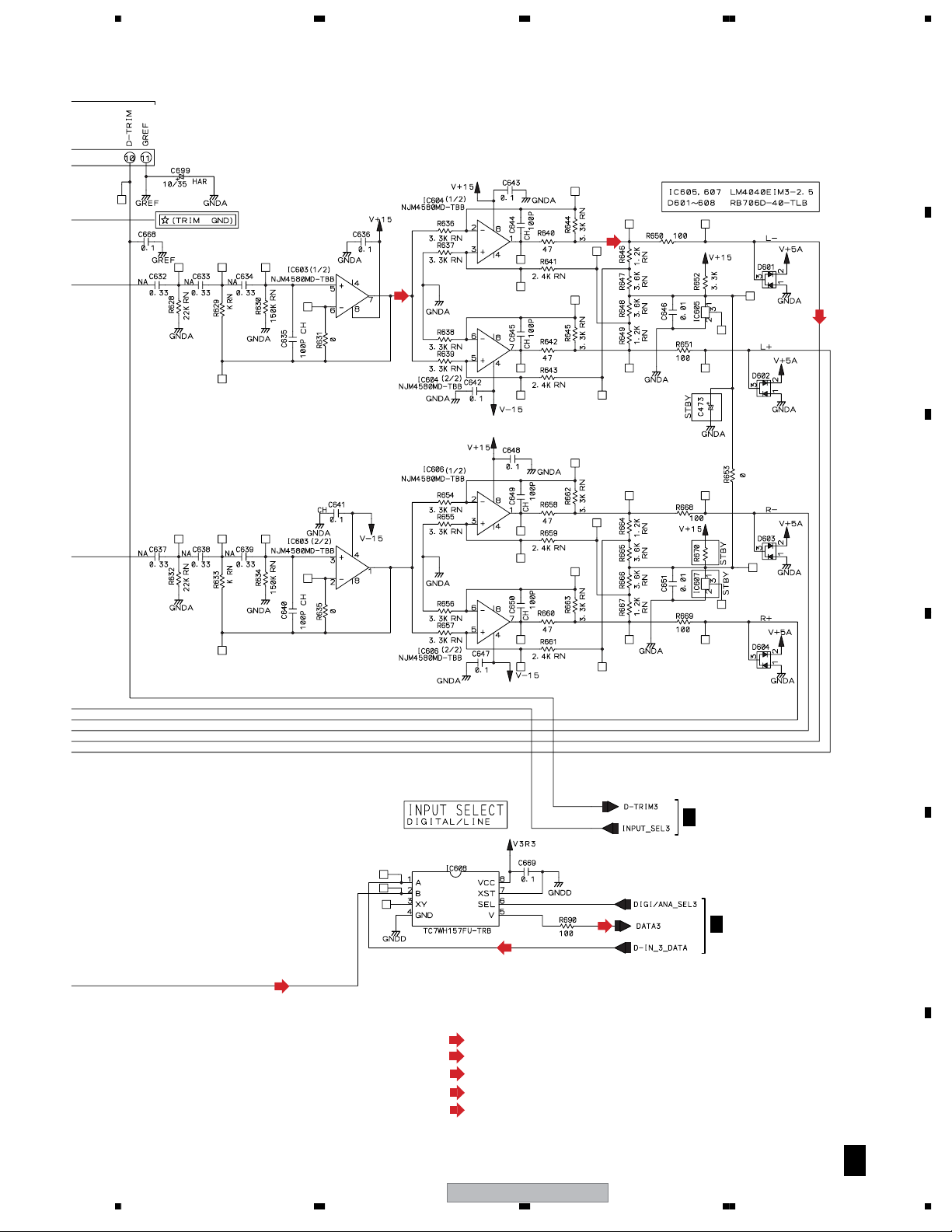
DIGITAL/LINE
DIGITAL
CH 4
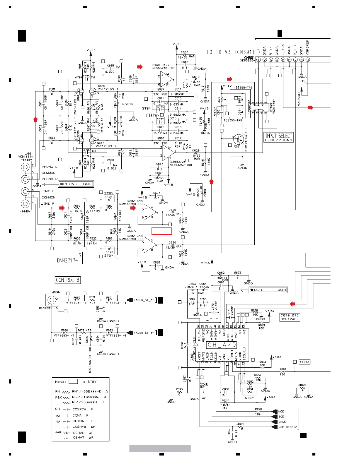
LINE/DIGI TAL
PHONO SW.
LINE/DIGI TAL
LINE
DIGITAL
PHONO
PHONO
PHONO
PHONO
LINE/CD
ANALOG
DIGITAL
119
MATRIX
21
same as CH 3
F
-COM
VR AD
PHONO/LINE SW .
DIGIT AL SEL.
DIGITAL
/ANALOG SW.
A/D
SRC
-COM
VR AD
PHONO/LINE SW .
DIGIT AL SEL.
DIGITAL
/ANALOG SW.
To DSP BLOCK DIAGRAM
29
30
145
146
CH 3
CH 4
12
DJM-800
1234
Page 13
5678
A
D610A003BPYPA225-K
DSP
PHONES
MASTER
BOOTH
REC
SEND
RETURN
13
27
20
18
17
150
D/A
MASTER ATT.
D/A
SRC DIT
BUFFER AMP.
D/A
BUFFER
D/A
D/A
A/D
BUFFER
AMP.
AMP.
MUTE
MUTE
MUTE
MUTE
MUTE
MUTE
PHONES
B
MASTER 1
MASTER 2
DIGITAL OUT
BOOTH
REC
C
SEND
D
RETURN
64M 4M
SDRAM
÷
When ordering service parts, be sure to refer to "EXPLODED VIEWS and PARTS LIST" or
FLASH
ROM
FPGA
XC3S50-
4TQG144C-K
-COM
HD64F2377-K
(PEG236A8-K)
"PCB PARTS LIST".
÷
The > mark found on some component parts indicates the importance of the safety factor
of the part. Therefore, when replacing, be sure to use parts of identical designation.
÷
: The power supply is shown with the marked box.
DJM-800
56
7
E
F
13
8
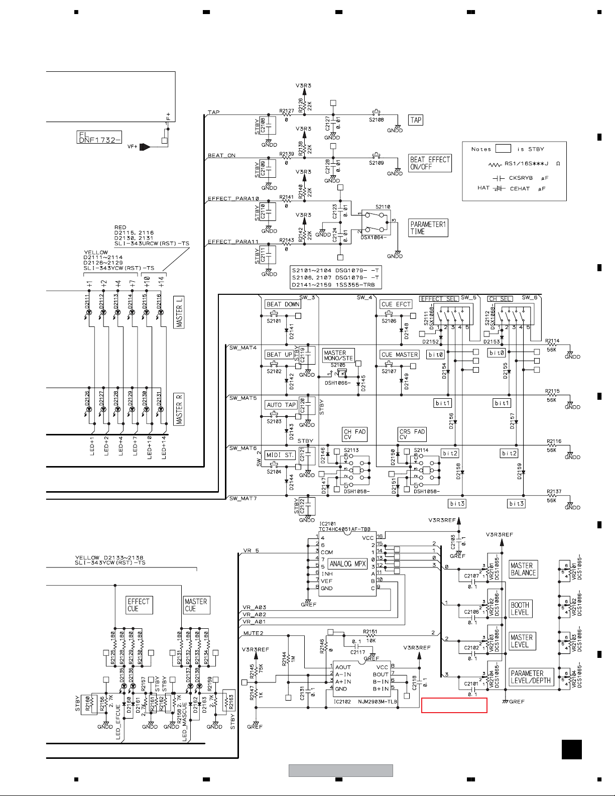
Page 14
1234
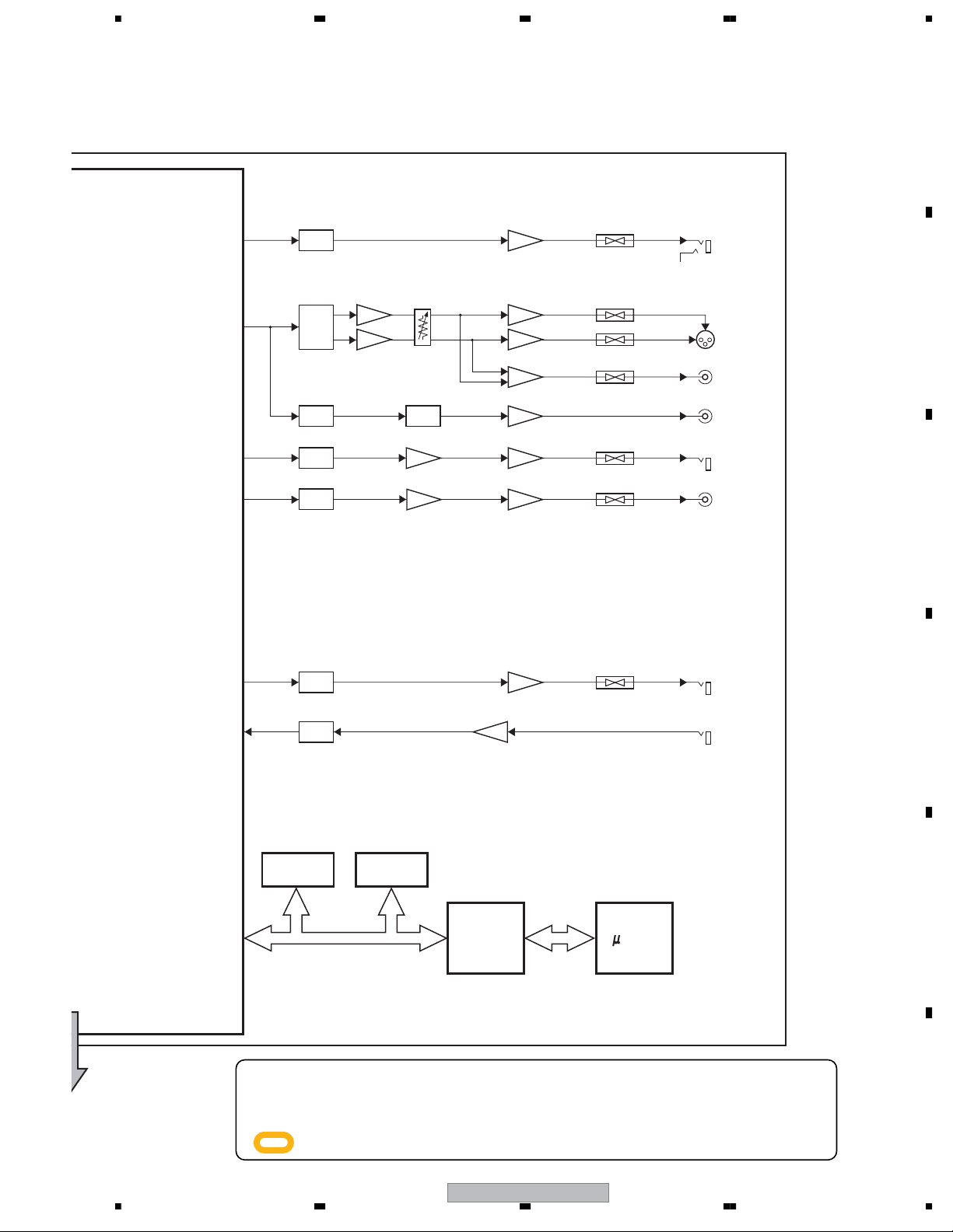
S
1
–
s
3.2 OVERALL BLOCK DIAGRAM_2
A
I
DSP BLOCK DIAGRAM
DJM-800 Audio DSP
CHn In
Digital in
Analog in
Input of digital / analog is set by SelectSW
B
MIC1,2 In
C
CH1-CH4 COMMON
Digital Trim
2Band
MIC
EQ
BPM
detect
CHx
MIC1,2
MIX
3Band
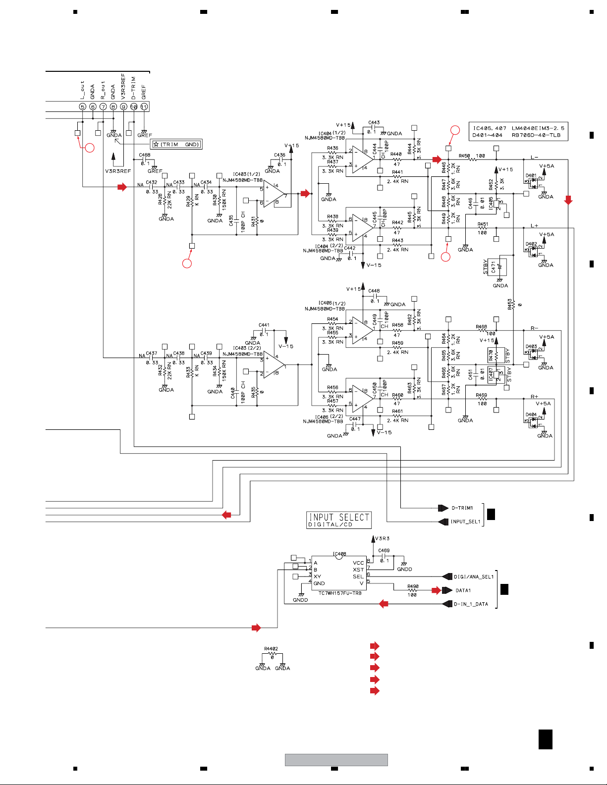
CHn
EQ
COLOR
EFFECTS
[ch1–4]
MIC SW
Off
On
TalkOver
3-possi.
BEAT
EFFECTS
[CHx(pre)]
∗1 ∗2,3
Send
Return
[CHx]
∗2,3,4
BPM
detect
[MIC]
∗5
CUE
Monitor
[CHx]
EFFECTS
BEAT
[MIC]
Send
Return
[MIC]
∗2,4
CHn Fader CF Assign
CH
Fader
Curve
3-possi.
CHx Level Meter CHx
Master
Balance
BEAT
EFFECTS
[CHx(post)]
MIC Data
Thru
CF_A
CF_B
3-possi.
CHx
+
+
CROSS
Fader
Cross
Fader
Curve
3-possi.
BPM
detect
[CF_A]
∗5 ∗4
BPM
detect
[CF_B]
∗5 ∗4
Send
Return
[CF_A]
Send
Return
[CF_B]
D
E
FPGA
[Dual PortRAM]
Send Out
Return In
MIC
Filter
• Mode
CPU
• Volume data
I/F
• Switch data
Bus
Logic
• CH Fader position
• CF Fader position
• Control Command
BEAT
EFFECTS
(SND/RTN)
/// BEAT EFFECT (SND/RTN) /// /// COLOR EFFECT (Harmonic) ///
EFFECT CH SELECT
–4
CH1
CF_A/B
MIC
Master
Return In
EFFECT CH SELECT
Return Level Effect SW
–4
CH1
CF_A/B
MIC
Master
No Cable EFFECT Processor CH
Cable Exist
CableCheck
SEND Out
Effect Out
EFFECT CUE
Talk Over On/Off
CH1
–4 In Friqency Counter
Effect Contror (from CPU)
∗1 : Ch1
∗2 : Boil
∗3 : Po
∗4 : I do
∗5 : I de
/// BEAT EFFECT (Other) ///
EFFECT CH SELECT
CH1
–4
F
CF_A/B
MIC
Master
EFFECT Processor
MIX RATIO Effect Out
14
Effect SW CH1–4 In EFFECT Processor CH1
EFFECT CUE
DJM-800
/// COLOR EFFECT (Others) ///
1234
Page 15
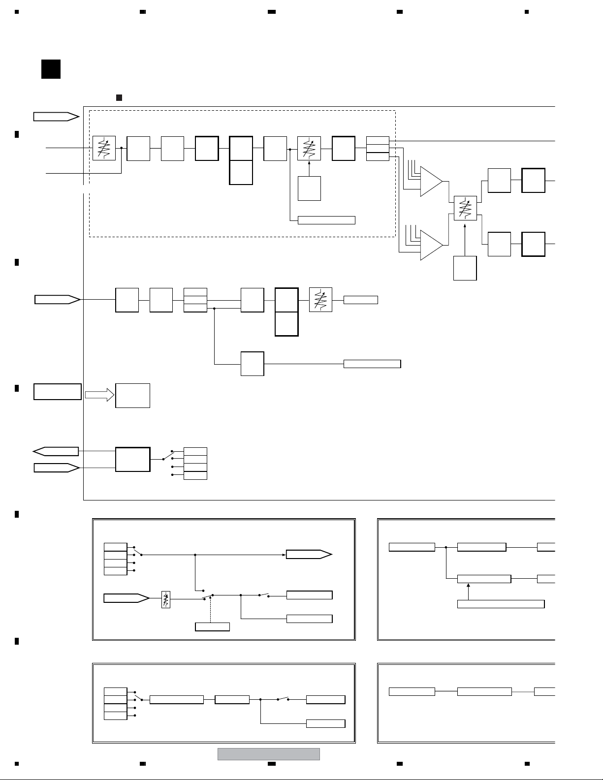
5678
t
o
t
t
A
Master
Balance Talk Over
Talk Over On/Off
MIC Monitor SW CHx MIX Data
∗2,4
Master
Mono
Stereo
MIC Data
BPM
M
Send
Return
ect
[CF_A]
_A]
∗5 ∗4 ∗2,3
M
Send
Return
ect
[CF_B]
_B]
∗5 ∗4 ∗2,3
∗1 : Ch1 – 4 processes the same effect.
∗2 : Boil
∗3 : Position of effect input is set in either front and back of fader by specification of Effect.
∗4 : I do SEND/RETURN of CH set in SND/RTN select by EffectCHSELECT.
∗5 : I detect B P M of CH selected by EFFECT CHSELECT.
BEAT
EFFECTS
[CF_A(post)
BEAT
EFFECTS
[CF_B(post)
effectch Select
+
SW and do of effect attention for selected setting.
detect
[Master]
BEAT
EFFECTS
[Master]
∗5
Send
Return
[Master]
MIC Data
+
CHx CUE
Effect CUE
Master Level
Master CUE
+
Booth Level
+
• DSP Status
• BPM Detect data
• Harmonic Detect data
• CH Level Meter
• Master Level Meter
Master Level Meter
H.P.
MIX
EFFECT
Processor
H.P. Level
CPU
I/F
Logic
Rec Out
Master Out1
Master Out2
Digital Out
H.P. Out
Booth Out
FPGA
[Dual PortRAM]
SD-RAM
B
C
D
/// BPM DET. ///
EFFECT CH SELECT
CH1
er Send to CPU
ssor CH1–4 Out
r (from CPU)
ssor CH1–4 Out Mono Split
56
–4
CF_A/B
MIC
Master
∗ I detect B P M only for CH which EFFECT CH SELECT appears, and was Counter.
/// H.P. MIX ///
CHx CUE
EFFECT CUE
Master CUE L
BPM COUNTER
CUE Balance
+
Master Balance H.P.Level
L
R
R
Send to CPU
H.P.MONOSPLIT/STEREO SW
Mono Split
Stereo
Stereo
+
+
H.P.Level
DJM-800
7
E
H.P. Out Lch
F
H.P. Out Rch
15
8
Page 16
1234
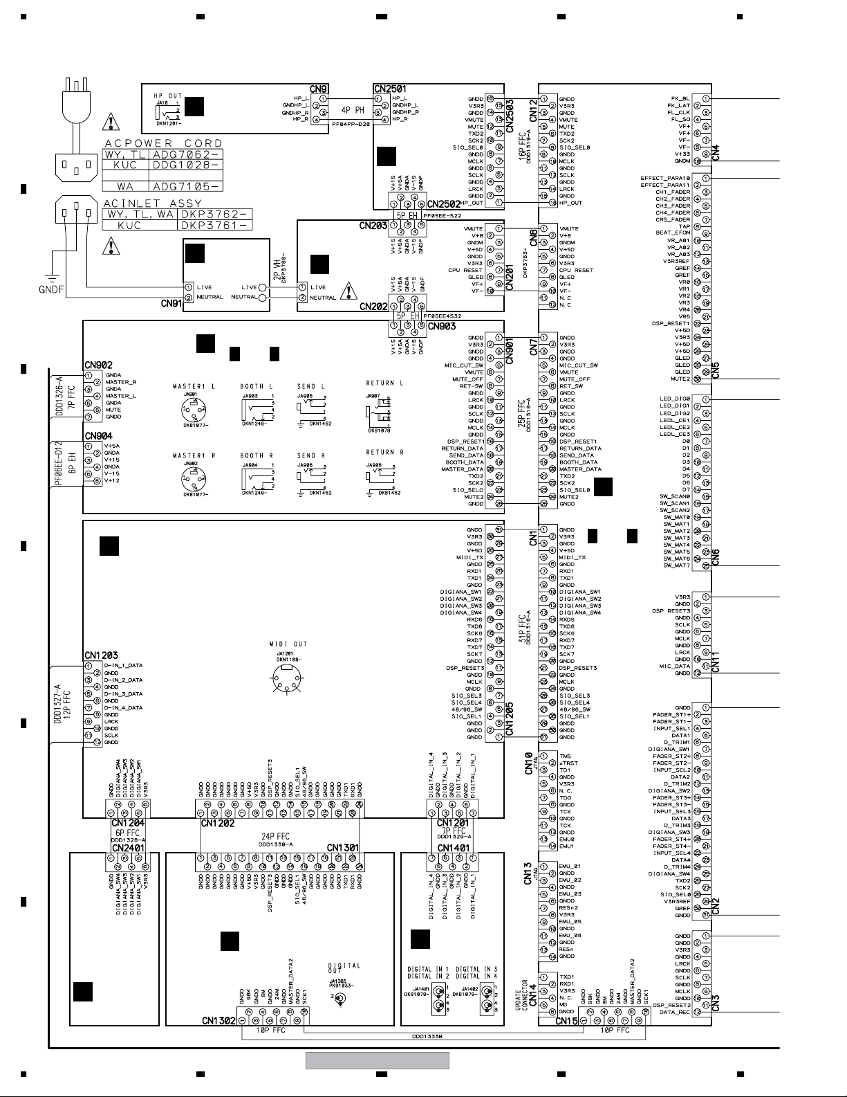
3.3 OVERALL WIRING DIAGRAM
A
B
C
P
HP JACK(DWX2553)
ACSW
R
(DWX2545)
OUTPUT(DWX2544)
J
J J
1/3–( 3/3)
O
SW POWER SUPPLY
Q
HPAMP
(DWX2556)
I
DSP
(DWX2534)
I I
DIGIC(DWX2547)
K
1/3–( 3/3)
D
E
DIGIB(DWX2546)
M
F
SLSW
N
(DWX2536)
DIGIA
L
(DWX2555)
16
DJM-800
1234
Page 17
5678
PANEL1(DWX2552)
C
G 1/4
CHFD1(DWX2537)
G 2/4
CHFD2(DWX2538)
G 3/4
CHFD3(DWX2539)
G 4/4
CHFD4(DWX2540)
H
CRSFD(DWX2541)
PANEL2(DWX2554)
F
A
B
C
A
INPUT
(DWX2535)
A A
1/6–( 6/6)
MIC1
B
(DWX2542)
MIC2
E
(DWX2543)
D
D 4/4
TRIM1(DWX2548)
D 3/4
TRIM2(DWX2549)
E
D 2/4
TRIM3(DWX2550)
D 1/4
TRIM4(DWX2551)
F
56
DJM-800
17
7
8
Page 18
1234
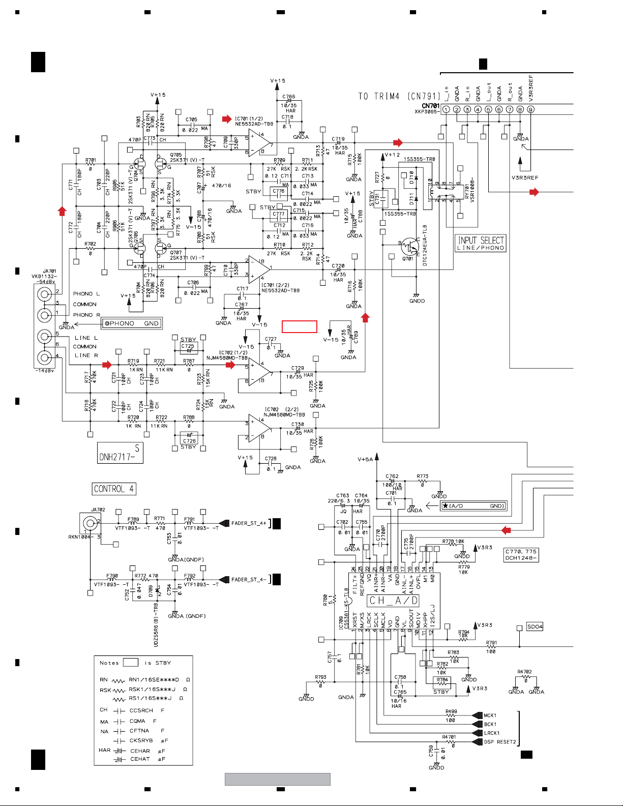
3.4 INPUT ASSY (1/6)
A
B
C
A 1/6
(LI)
INPUT ASSY(DWX2535)
8
(LI)
BUFFER
1
(CDI)
(CDI)
BUFFER
CN491
4/4
D
(LI)
9
(CDI)
2
Shield Case
D
Analogue
6/6
A
6/6A
E
7
F
18
2/6,3/6,4/6,6/6A
A 1/6
DJM-800
1234
Page 19
5678
A
5
3
_
(CH1)
(CH1)
(CH1)
(CH1)
B
1212
4
6
C
D
(CH1)
(D1)
(CH1D)
AUDIO SIGNAL ROUTE
(LI)
: LINE INPUT L CH SIGNAL
(CDI)
: CD INPUT L CH SIGNAL
(CH1)
: CH1 L CH SIGNAL
(D1)
(CH1Y)
: CH1 DIGITAL SIGNAL
: CH1 Y CH SIGNAL
DJM-800
56
6/6A
(CH1Y)
6/6A
E
F
A 1/6
19
7
8
Page 20
1234
3.5 INPUT ASSY (2/6)
A
A 2/6
INPUT ASSY(DWX2535)
CN591
3/4
D
(PI)
10
11
B
C
(PI)
_
(CDI)
(CDI)
12
(PI)
13
(CH2)
(CDI)
BUFFER
Shield Case
D
6/6
A
Analogue
(CH2)
6/6A
E
17
F
20
A 2/6
1/6,3/6,4/6,6/6A
DJM-800
1234
Page 21

5678
A
15
_
(CH2)
1212
14
(CH2)
16
(CH2)
B
C
(CH2D)
(D2)
AUDIO SIGNAL ROUTE
(PI)
: PHONO INPUT L CH SIGNAL
(CDI)
: CD INPUT L CH SIGNAL
(CH2)
: CH2 L CH SIGNAL
(D2)
(CH2Y)
: CH2 DIGITAL SIGNAL
: CH2 Y CH SIGNAL
(CH2Y)
D
6/6A
E
6/6A
F
56
DJM-800
A 2/6
21
7
8
Page 22
1234
3.6 INPUT ASSY (3/6)
A
A 3/6
INPUT ASSY(DWX2535)
(PI)
(PI)
CN691
2/4
D
(CH3)
B
C
D
(PI)
(LI)
Shield Case
_
(LI)
BUFFER
(LI)
E
F
22
A 3/6
Analogue
A
6/6
(CH3)
6/6A
1/6,2/6,4/6,6/6A
DJM-800
1234
Page 23
5678
A
_
(CH3)
1212
(CH3)
(CH3)
B
C
(CH3D)
AUDIO SIGNAL ROUTE
(PI)
: PHONO INPUT L CH SIGNAL
(LI)
: LINE INPUT L CH SIGNAL
(CH3)
: CH3 L CH SIGNAL
(D3)
(CH3Y)
: CH3 DIGITAL SIGNAL
: CH3 Y CH SIGNAL
(D3)
(CH3Y)
D
6/6A
E
6/6A
F
56
DJM-800
A 3/6
23
7
8
Page 24
1234
3.7 INPUT ASSY (4/6)
A
B
A 4/6
INPUT ASSY (DWX2535)
(PI)
(PI)
(PI)
CN791
1/4
D
(CH4)
_
C
(LI)
(LI)
Shield Case
D
A
BUFFER
6/6
(LI)
Analogue
(CH4)
6/6A
E
F
24
1/6,2/6,3/6,6/6A
A 4/6
DJM-800
1234
Page 25
5678
A
_
(CH4)
(CH4)
B
1212
(CH4)
C
(CH4D)
AUDIO SIGNAL ROUTE
(PI)
: PHONO INPUT L CH SIGNAL
(LI)
: LINE INPUT L CH SIGNAL
(CH4)
: CH4 L CH SIGNAL
(D4)
(CH4Y)
: CH4 DIGITAL SIGNAL
: CH4 Y CH SIGNAL
(D4)
(CH4Y)
D
6/6A
E
6/6A
F
56
DJM-800
A 4/6
25
7
8
Page 26
1234
3.8 INPUT ASSY (5/6)
A
B
C
A 5/6
6/6A
6/6A
INPUT ASSY (DWX2535)
(RECD)
(REC)
18
(REC)
19
D
(MA)
6/6A
E
BUFFER
(MA)
6/6A
F
26
A 5/6
DJM-800
1234
Page 27
5678
A
B
(REC)
22
20
MUTE
(MA)
(REC)
C
23
(MA)
(REC)
21
D
AUDIO SIGNAL ROUTE
(RECD)
: REC DIGITAL CH SIGNAL
(REC)
: REC L CH SIGNAL
(MA)
: MASTER L CH SIGNAL
DJM-800
56
E
F
A 5/6
27
7
8
Page 28
1234
3.9 INPUT ASSY (6/6)
A
B
C
A 6/6
CN3
INPUT ASSY (DWX2535)
28
27
1/3
I
24
26
25
A
5/6
LRCK BUFFER
BCK BUFFER
1/6,2/6,3/6,4/6
A
(CH1Y)
D
(CH2Y)
CN2
1/3
I
E
(CH3Y)
(CH4Y)
1/6A
2/6A
3/6A
AUDIO SIGNAL ROUTE
(CH1Y)
4/6A
(CH2Y)
(CH3Y)
(CH4Y)
5/6A
: CH 1 Y CH SIGNAL
: CH 2 Y CH SIGNAL
: CH 3 Y CH SIGNAL
: CH 4 Y CH SIGNAL
(D1)
: CH1 DIGITAL SIGNAL
(D2)
: CH2 DIGITAL SIGNAL
(D3)
: CH3 DIGITAL SIGNAL
(D4)
: CH4 DIGITAL SIGNAL
(MA)
: MASTER L CH SIGNAL
F
28
A 6/6
DJM-800
1234
Page 29

5678
A
MCK BUFFER
BCK BUFFER
(D4)
(D1)
(D2)
(D3)
CN1203
1/6A
A
2/6
A
3/6
4/6
A
K
B
1/6,2/6,3/6,4/6A
5/6A
(MA)
CN902
1/3
J3/3
C
1/6,2/6,3/6,4/6A
LRCK BUFFER
MCK BUFFER
BCK BUFFER
LRCK BUFFER
CN904
J
1/6,2/6,3/6,4/6A
D
CN1501
B
5/6A
E
5/6A
5/6A
DJM-800
56
F
A 6/6
29
7
8
Page 30
1234
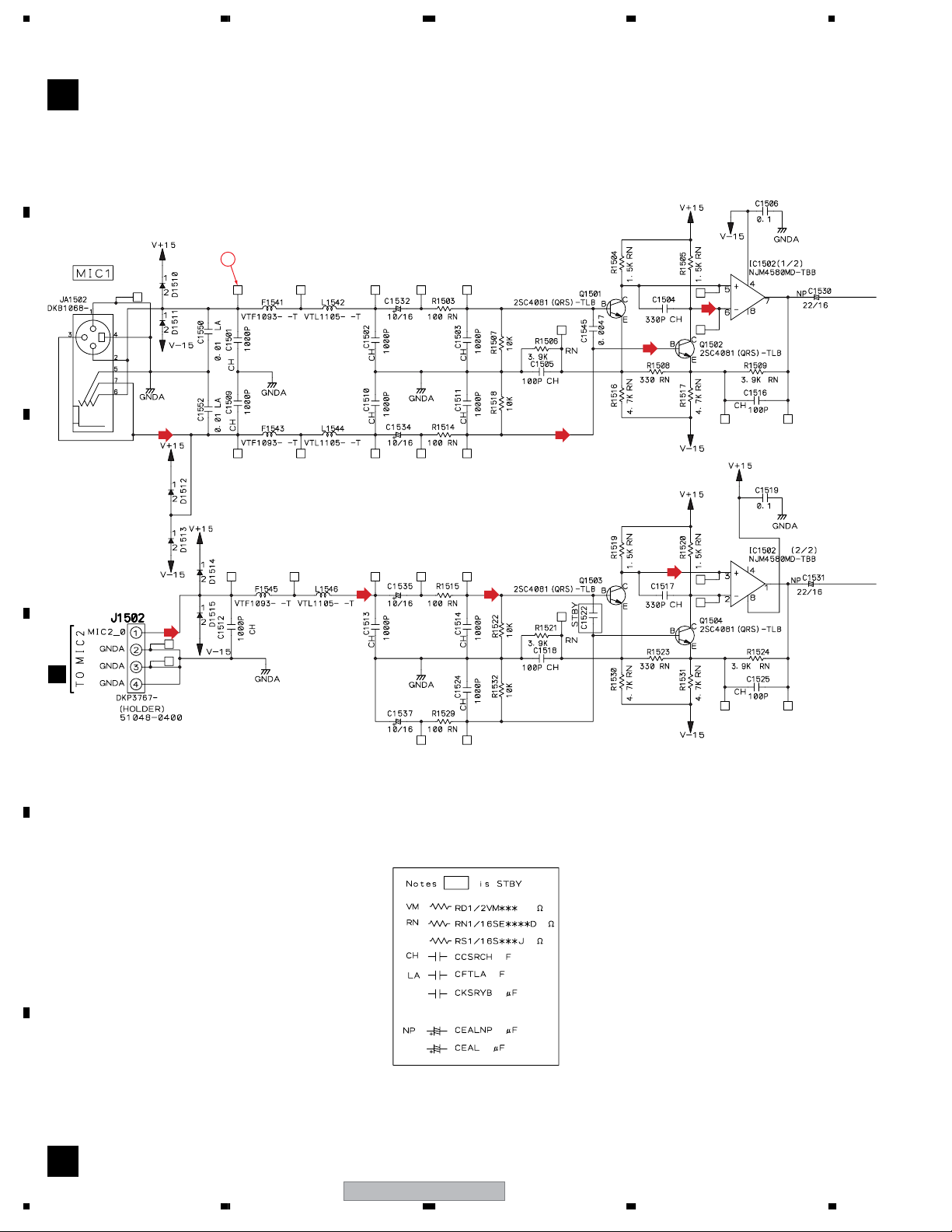
3.10 MIC 1 ASSY
MIC1 (DWX2542)
B
A
1
B
(MIC1)
(MIC1) (MIC1)
C
(MIC2) (MIC2)
(MIC2)
J1503
(MIC2)
(MIC1)
E
D
E
F
B
30
1234
DJM-800
Page 31

5678
A
2
(MIC1)
(MIC2)(MIC2)
(MIC1)
(MIC2)
3
B
CN456
(MIC1)
6/6
A2/3
C
(MIC2)
MIC A/D
7
6 5
D
(MIC1)
(MIC1)
C
Signal
(MIC2)
CN1704
DJM-800
56
AUDIO SIGNAL ROUTE
(MIC1)
: MIC1 L CH SIGNAL
(MIC2)
: MIC2 L CH SIGNAL
(MICD)
: MIC DIGITAL CH SIGNAL
7
(MICD)
CN11
I
4
E
F
B
31
8
Page 32

1234
3.11 PANEL 1 ASSY
PANEL1 ASSY (DWX2552)(1/2)
C
A
Large size
SCH diagram
1/2
B
F
CN2101
C
D
E
2/2
1/2
F
32
1234
DJM-800
Page 33

5678
F
CN2102
CURVE CHRST
A Curve
Special Curve
B Curve
B Curve
CLICK Exist/Noexist
No exist
Exist
Exist
No exist
A
B
C
D
E
56
DJM-800
F
33
7
8
Page 34

1234
A
C
PANEL1 ASSY
(DWX2552)(2/2)
B
CN2608
H
C
CN2604
G
Large size
CN2603
SCH diagram
G 4/4
1/2
D
CN2602
G 3/4
CN2601
1/4
G 2/4
E
2/2
F
34
2/2
CN4
1/3
I
DJM-800
1234
I
1/3
CN5
Page 35

5678
A
B
C
D
E
CN6
1/3
I
DJM-800
56
F
CN1503
B
35
7
8
Page 36

1234
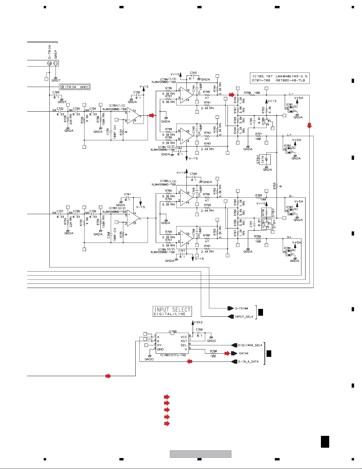
3.12 TRIM1 to TRIM 4 ASSYS
A
D 4/4
B
TRIM1 ASSY (DWX2548)
D 3/4
TRIM2 ASSY (DWX2549)
C
CN401
A
D 2/4
D
E
TRIM3 ASSY (DWX2550)
D 1/4
TRIM4 ASSY (DWX2551)
CN501
2/6
A1/6
CN601
A
F
CN701
4/6
A3/6
D 1/4–4/4 D 1/4–4/4
36
1234
DJM-800
Page 37

5678
3.13 MAIC 2 ASSY
MIC2 (DWX2543)
E
A
B
Earth Plate
AUDIO SIGNAL ROUTE
(MIC2)
: MIC2 L CH SIGNAL
(MIC2)
J1502
B
C
D
E
E
56
DJM-800
F
E
37
7
8
Page 38

1234
3.14 PANEL 2 ASSY
PANEL2 ASSY (DWX2554)
F
A
B
CN1710
C
C
D
CN1711
C
E
F
F
38
1234
DJM-800
Page 39
Holder
5678
A
B
C
D
E
56
DJM-800
MASTER VOL LEVEL
ZERO DETECTOR
7
F
F
39
8
Page 40
1234
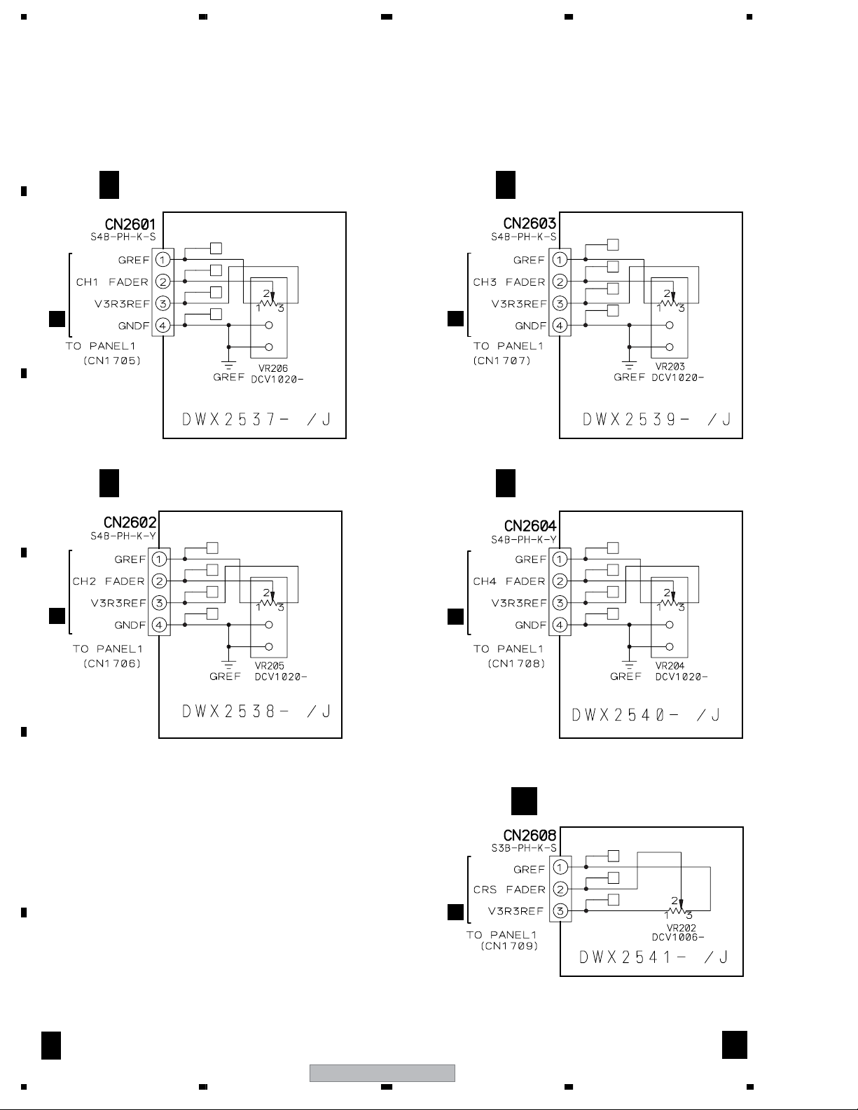
3.15 CHFD 1 to CHFD 4 and CRSFD ASSYS
A
G 1/4
B
CN1705
C
C
G 2/4
CHFD1(DWX2537)
CHFD2(DWX2538)
G 3/4
CN1707
C
G 4/4
CHFD3(DWX2539)
CHFD4(DWX2540)
CN1706
C
D
E
F
CN1708
C
CN1709
C
CRSFD(DWX2541)
H
G 1/4–4/4
40
1234
H
DJM-800
Page 41

5678
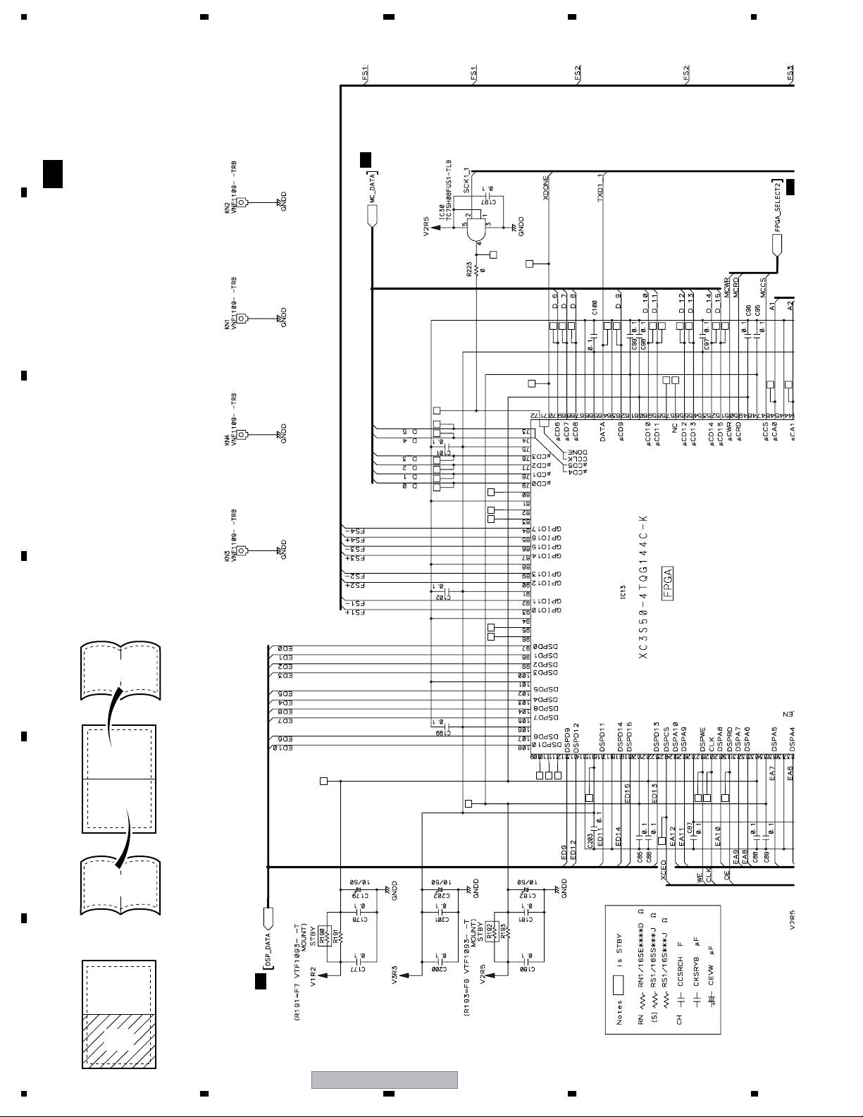
3.16 DIGIA ASSY
DIGIA ASSY (DWX2555)
L
K
A
CN1201
B
(D1)
(D2)
(D3)
(D4)
AUDIO SIGNAL ROUTE
(D1)
: CH1 DIGITAL SIGNAL
(D2)
: CH2 DIGITAL SIGNAL
(D3)
: CH3 DIGITAL SIGNAL
(D5)
: CH4 DIGITAL SIGNAL
C
D
E
L L
56
DJM-800
7
8
F
41
Page 42

1234
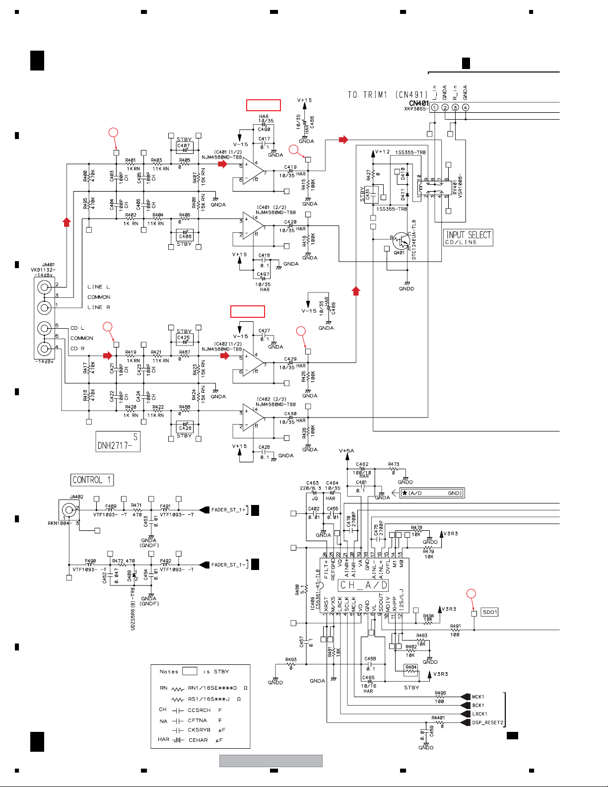
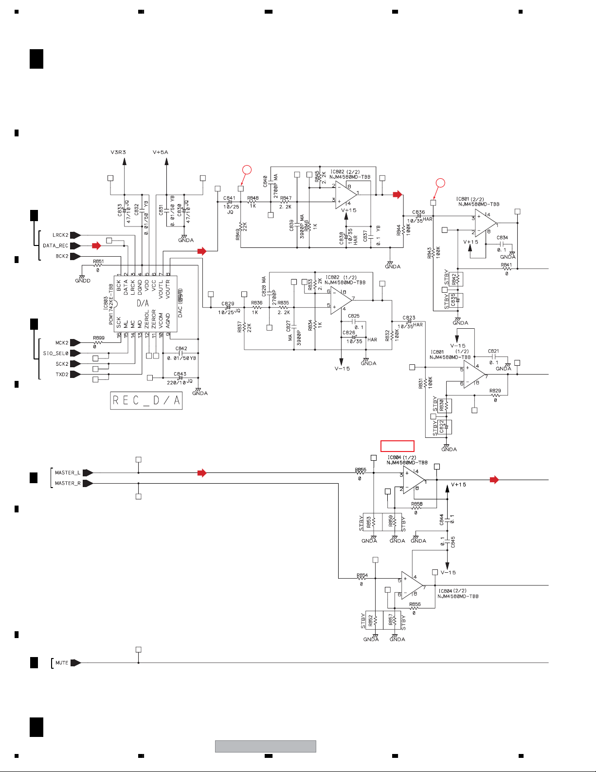
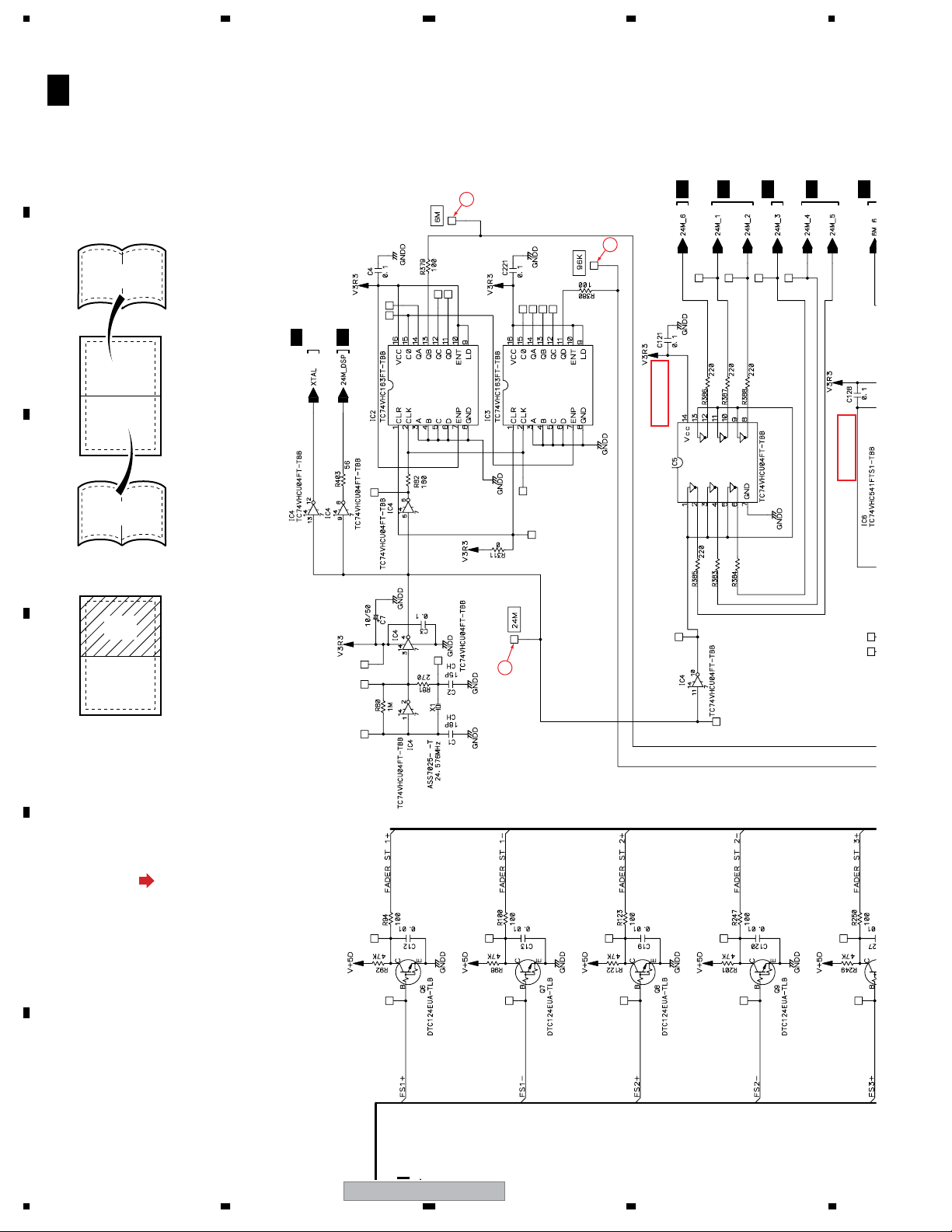
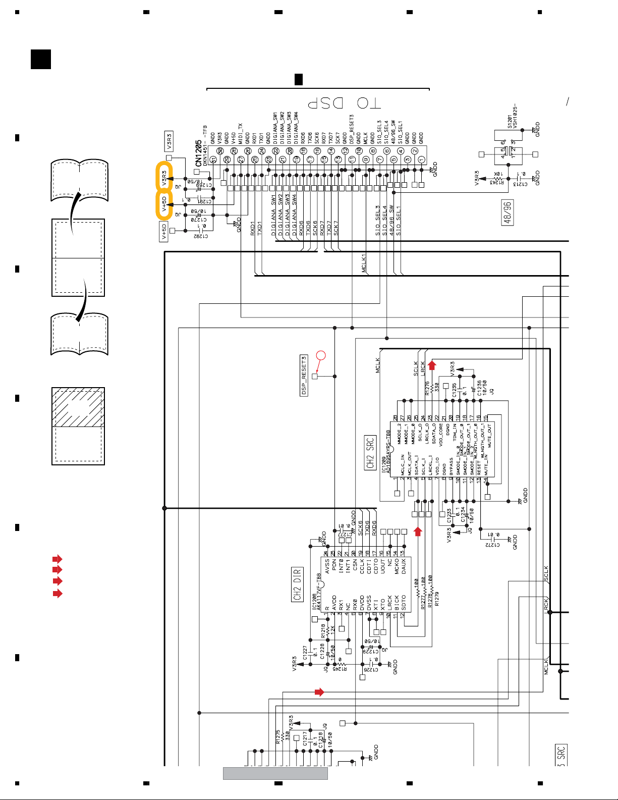
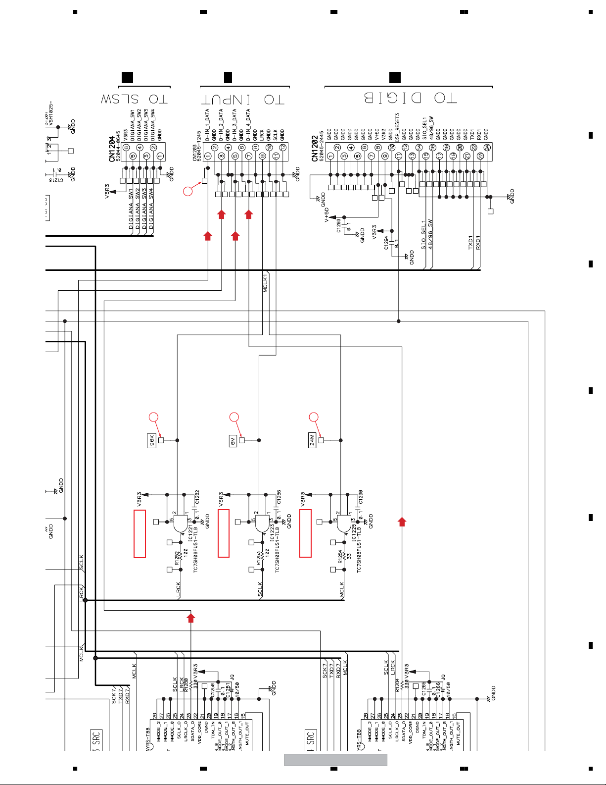
3.17 DSP ASSY (1/3)
A
B
C
I 1/3
DSP ASSY (DWX2534)(1/2)
Large size
SCH diagram
1/2
2/2
C
CN1701
C
CN1702
1/3,2/3I
1/2
3/3I
D
3/3I
E
AUDIO SIGNAL ROUTE
(SDD)
: SEND DIGITAL SIGNAL
(RND)
: RETURN DIGITAL SIGNAL
(BOD)
(MA1D)
: BOOTH DIGITAL SIGNAL
: MASTER DIGITAL SIGNAL
F
42
1234
DJM-800
Page 43

5678
A
C
CN1703
CN901
1/3
J
B
(RND)
(BOD)
1/3,2/3I
3/3
1/3I
I
(SDD)
(MA1D)
1/3,2/3I
C
I
1/3,2/3
I
2/3
I
BUFFER
2/3
1/3I
D
1/3,2/3I
E
BUFFER
3/3I
F
DYW1757
DJM-800
56
43
7
8
Page 44

1234
A
I 1/3
DSP ASSY
(DWX2534)(2/2)
B
3/3I
C
Large size
SCH diagram
1/2
2/3,3/3I
D
1/3
I
1/3,2/3I
3/3
2/2
E
I 2/3I
3/3I
3/3I
I
2/2
F
AUDIO SIGNAL ROUTE
(CH1Y)
(CH2Y)
44
: SCH 1 Y CH SIGNAL
: SCH 2 Y CH SIGNAL
DJM-800
1234
O
CN2503
K
CN1205
Page 45
5678
5
DYW17
1/3I
3/3
I
A
B
C
3/3
3/3I
2/3I
D
UPDATE
CONNECTOR
3/3I
1/3,2/3I
I
3/3
(CH1Y) (CH2Y) (CH3Y) (CH4Y)
(RECD)
1/3I
3/3I
E
K
CN1205
CN452
6/6
A 6/6
56
DJM-800
F
CN451
A
7
8
45
Page 46

1234
3.18 DSP ASSY (2/3)
A
B
C
I 2/3
DSP ASSY (DWX2534)(1/2)
Large size
SCH diagram
1/2
2/2
CN1502
B
1/3I 3/3I
1/2
D
E
F
46
1234
DJM-800
Page 47

5678
A
B
3/3I
C
3/3I
D
3/3I
1/3,2/3I
E
1/3I
56
DJM-800
F
47
7
8
Page 48

A
I 2/3
DSP ASSY
(DWX2534)
(2/2)
B
1234
Large size
C
SCH diagram
(CH2Y)
(CH4Y)
(CH1Y)
(CH3Y)
1/2
D
2/2
1/3I
1/3,3/3I
E
2/2
I
AUDIO SIGNAL ROUTE
(CH1Y)
(CH2Y)
(MA1D)
(MA2D)
(RECD)
F
48
: SCH 1 Y CH SIGNAL
: SCH 2 Y CH SIGNAL
: MASTER DIGITAL CH SIGNAL
: MASTER DIGITAL CH SIGNAL
: REC DIGITAL CH SIGNAL
(BOD)
: BOOTH DIGITAL CH SIGNAL
(SDD)
: SEND DIGITAL CH SIGNAL
(HPD)
: HP DIGITAL CH SIGNAL
SUPPLY
POWER
Q
CN201
DJM-800
1234
Page 49

5678
A
3/3
1/3I
I
1/3I
1
B
2
(MA1D)
(MA2D)
5
(HPD)
(RECD)
(BOD)
(SDD)
C
3
4
D
E
1/3,2/3I
3/3I
F
56
DJM-800
7
8
49
Page 50
3
1234
3.19 DSP ASSY (3/3)
I 3/3
A
Large size
SCH diagram
B
C
DSP ASSY (DWX2534)(1/2)
1/2
1/3I 2/3I
2/2
7
8
3/3I 2/3I
24M BUFFER
I1/3I 1/3I
6M BUFFER
R384=L5
R383=L8
L5=CTF1346
L8=CTF1357
1/2
6
D
AUDIO SIGNAL ROUTE
(MA2D)
E
: MASTER DIGITAL CH SIGNAL
F
50
1234
DJM-800
Page 51

3 3/3I 2/3I 2/3I 3/3I 2/3I 2/3I 1/3I1/3I1/3I 1/3I1/3I
5678
A
CN1302
M
B
(MA2D)
=L6
=L9
=L7
=L10
1/3I
6M BUFFER
L6, L9=CTF1357
96k BUFFER
L7, L10=CTF1357
3/3I
2/3I
C
1/3I
D
56
DJM-800
E
F
51
7
8
Page 52
1234
A
I 3/3
DSP ASSY
(DWX2534)(2/2)
B
1/3I
I
C
Large size
SCH diagram
D
1/2
E
2/2
2/3I
F
2/2
52
1234
DJM-800
Page 53

5678
A
1/3I
1/3I
B
1/3I
C
1/3,2/3I
D
1/3I
E
2/3I
DJM-800
56
1/3I
F
53
7
8
Page 54

1234
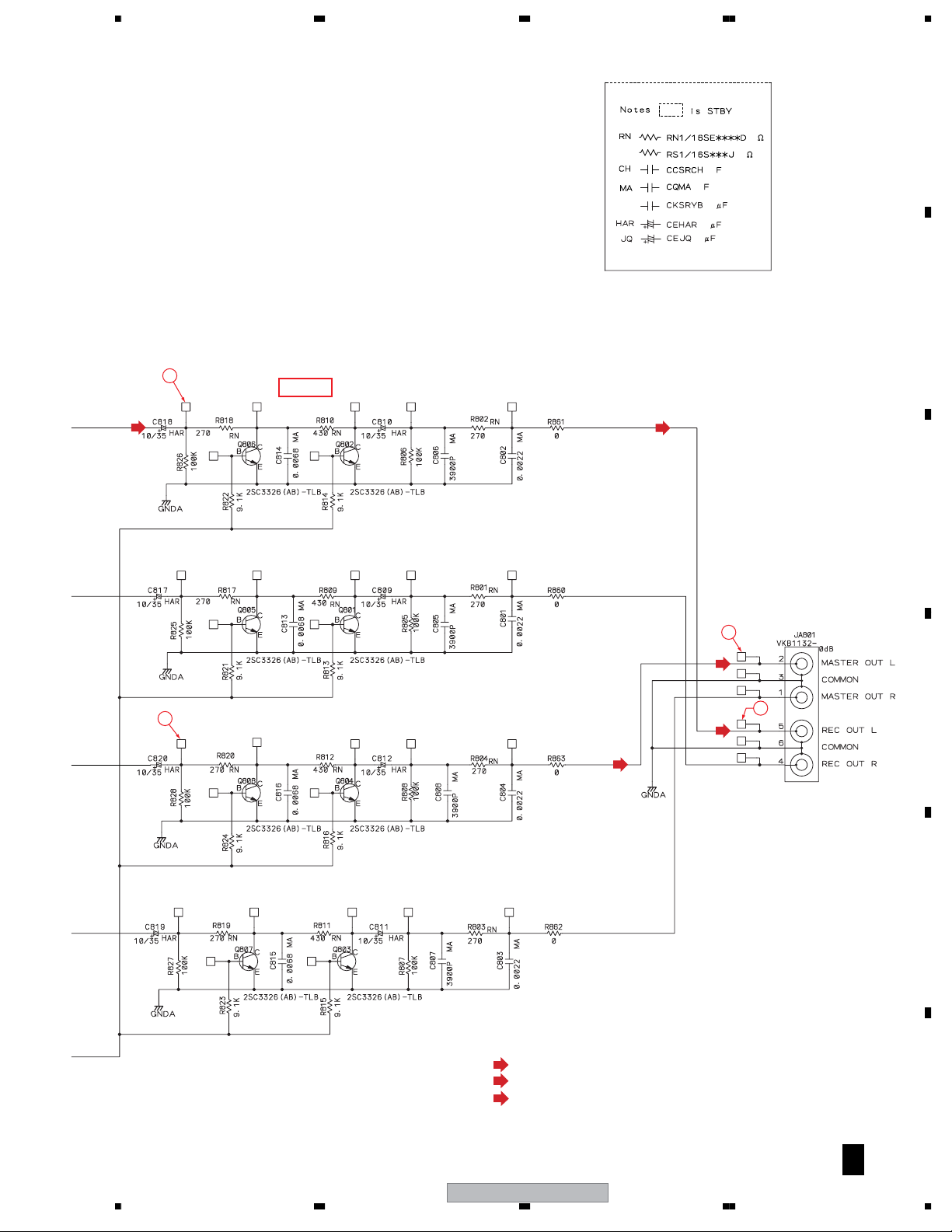
3.20 OUTPUT ASSY (1/3)
A
B
C
J 1/3
CN7
1/3
I
OUTPUT ASSY (DWX2544)
3/3J
22 262425
3/3
J
3/3J
J
(MA1D)
2/3,3/3
J
16
8
1
23
2/3
MCK BUFFER
2
(MA)
3
2/3,3/3J
BCK
BUFFER
D
LRCK
BUFFER
2/3,3/3J
2/3,3/3J
E
2/3,3/3J
F
54
J 1/3
DJM-800
1234
Page 55

5678
A
(MA)
(MA)
Shield Case
(MA)
4
(MA)
7
(MA)
(MA)
6
(MA)
B
5
C
(MA)
D
E
(MA)
AUDIO SIGNAL ROUTE
(MA)
CN454
6/6
A
(MA1D)
: MASTER L CH SIGNAL
: MASTER DIGITAL CH SIGNAL
F
56
DJM-800
J 1/3
55
7
8
Page 56

1234
3.21 OUTPUT ASSY (2/3)
A
B
C
J 2/3
1/3,3/3J
1/3
J
1/3,3/3
J
OUTPUT ASSY (DWX2544)
9
(BO)
(BOD)
10
Signal
1/3,3/3J
D
E
1/3,3/3
J
F
56
J 2/3
DJM-800
1234
Page 57

5678
A
(BO)
11
12
13
(BO)
(BO)
B
15
14
C
AUDIO SIGNAL ROUTE
(BO)
: BOOTH L CH SIGNAL
(BOD)
: BOOTH DIGITAL CH SIGNAL
D
E
F
56
DJM-800
J 2/3
57
7
8
Page 58

1234
3.22 OUTPUT ASSY (3/3)
A
B
C
J 3/3
1/3,2/3J
1/3J
1/3,2/3J
1/3,2/3J
OUTPUT ASSY (DWX2544)
(SDD)
17
(SD)
(SD)
1/3,2/3J
D
20
(RN)
E
BUFFER
21
(RN)
(RN)
F
58
J 3/3
DJM-800
1234
Page 59

5678
A
18
19
(SD)
B
C
Signal
(RND)
CN455
6/6
A
D
CN202
Q
E
1/3J
Powe r
Supply
1/3J
AUDIO SIGNAL ROUTE
(SD)
: SEND L CH SIGNAL
(SDD)
: SEND DIGITAL CH SIGNAL
(RN)
: RETURN L CH SIGNAL
1/3J
(RND)
: RETURN DIGITAL CH SIGNAL
F
56
DJM-800
J 3/3
59
7
8
Page 60
1234
3.23 DIGIC ASSY
DIGIC ASSY (DWX2547)(1/2)
K
A
Large size
SCH diagram
1/2
B
CN1
1/3
I
C
2/2
4
(D2)
1/2
D
AUDIO SIGNAL ROUTE
(D1)
: CH 1 DIGITAL SIGNAL
(D2)
: CH 2 DIGITAL SIGNAL
(D3)
: CH 3 DIGITAL SIGNAL
(D4)
E
: CH 4 DIGITAL SIGNAL
(D2)
(D1)
F
60
1234
DJM-800
Page 61
5678
N
CN2401
CN453
6/6
A
M
CN1301
3
(D2)
(D4)
(D1)
(D3)
A
B
C
6 7 5
LRCK BUFFER
(D3)
BCK BUFFER
D
(D4)
MCLK BUFFER
E
56
DJM-800
F
61
7
8
Page 62

1234
K
A
DIGIC ASSY
(DWX2547)(2/2)
2
B
(D1)
(D2)
Large size
SCH diagram
1/2
C
D
2/2
1
(D1)
(D1)
(D2)
2/2
E
(D2)
(D1)
AUDIO SIGNAL ROUTE
(D1)
: CH 1 DIGITAL SIGNAL
(D2)
: CH 2 DIGITAL SIGNAL
(D3)
: CH 3 DIGITAL SIGNAL
(D4)
: CH 4 DIGITAL SIGNAL
F
62
1234
DJM-800
Page 63

5678
A
(D3)
(D4)
B
(D3)
(D3)
(D4)
C
(D4)
D
L
(D3)
CN1401
(D4)
DJM-800
56
E
F
63
7
8
Page 64

1234
3.24 DIGIB ASSY
DIGIB ASSY (DWX2546)
M
A
B
2
(MA2D)
C
D
4
(D)
(D)
3
E
BUFFER
(D)
(D)
F
M
64
1234
DJM-800
Page 65

5678
A
LRCK
BUFFER
7
1
BCK
(D)
BUFFER
(MA2D)
CN15
3/3
I
B
6
MCLK BUFFER
5
C
(MA2D)
BUFFER
8
CN1202
K
D
(D)
AUDIO SIGNAL ROUTE
(D)
: DIGITAL CH SIGNAL
(MA2D)
: MASTER DIGITAL CH SIGNAL
DJM-800
56
E
F
M
65
7
8
Page 66

1234
3.25 HPAMP ASSY
HPAMP ASSY (DWX2556)
O
A
B
CN12
1/3
I
C
D
6
7
8
(HPD)
1
(HPD)
HP D/A
(HP)
2
E
Power Supply
CN203
Q
F
O
66
1234
DJM-800
Page 67

5678
A
B
3
C
(HP)
(HP)
4
5
(HP)
CN9
P
D
E
AUDIO SIGNAL ROUTE
(HP)
: HP L CH SIGNAL
(HPD)
: HP DIGITAL CH SIGNAL
DJM-800
56
F
O
67
7
8
Page 68

1234
A
B
3.26
HPJACKHPJACK
HPJACKHPJACK
HPJACK ASSY (DWX2553)
P
ASSYS
C
CN2501
O
D
AUDIO SIGNAL ROUTE
(HP)
: HP L CH SIGNAL
E
(HP)
F804=R1901
(R1901=0 )
F
P P
68
1234
DJM-800
Page 69

5678
3.27
R
ACSWACSW
ACSWACSW
ACSW (DWX2545)
ASSY
INLET ASSY
A
B
Q
C
TO SW POWER SUPPLY
D
E
R R
56
DJM-800
7
8
F
69
Page 70

1234
3.28 SW POWER SUPPLY UNIT
SW POWER SUPPLY UNIT (DWR1433)
Q
A
NOTE OF SPARE PARTS IN POWER SUPPLY (SYPS) UNIT
• In case of repairing, use the described parts only to prevent an accident.
• Please write the red mark on the board when the primary section of POWER SUPPLY (SYPS) Unit is repaired.
• Please take care to keep the space, not touching other parts when replacing the parts.
B
C
ASSY
ACSW
R
D
E
• NOTE FOR FUSE REPLACEMENT
F
CAUTION -
FOR CONTINUED PROTECTION AGAINST RISK OF FIRE.
REPLACE WITH SAME TYPE AND RATINGS ONLY.
Q
70
1234
DJM-800
Page 71

5678
A
B
CN 8
I 2/3
CN903
CN 2502
J
O
C
D
E
56
DJM-800
F
Q
71
7
8
Page 72

1234
3.29 VOLTAGES
Measurement Condition
A
B
C
D
E
Input
connectors
Output
connectors
MIC
CFX
FADER ST.
HP
CH
CRS FADER
MASTER
BOOTH MONITOR
CH FADER CURVE
CRS FADER CURVE
EFFECT
REAR
CD/LINE
PHONO
DIGITAL IN
RETURN
MIC1
MIC2
MASTER1
MASTER2
REC
BOOTH
SEND
DIGITAL OUT
HP
MIC LEVEL 1
MIC LEVEL 2
MIC EQ HI
MIC EQ LOW
MIC TKOV.
HP MONO/STEREO
MIXING
LEVEL
INPUT SELECT
TRIM
EQ HI
EQ MID
EQ LOW
COLOR
CUE
FADER
CROSS FADER ASSIGN
LEVEL
BALANCE
CUE
MONO/STEREO
AUTO/TAP
MIDI START/STOP
CUE
EFFECT
CHANNEL
TIME
LEVEL/DEPTH
ON/OFF
DIGI/ANA SEL
MASTER ATT.
MIC SIGNAL ADD/CUT
fs
Nothing
Nothing
Nothing
Nothing
Nothing
Nothing
Non connction
Non connction
Non connction
Non connction
Non connction
Non connction
Non connction
Max
Max
Center
Center
OFF
OFF(Lighting)
All Ch OFF
STEREO
Center
Max
All Fully counter clock wise direction
Max
Center
Center
Center
Center
ALL OFF
ALL Max
All Ch THRU
Center
Max
Center
OFF
STEREO
Max
Center
Center
AUTO
START
OFF
DERAY
1
–
Max
OFF(Lighting)
ALL DIGI
0dB
ADD
96K
F
72
1234
DJM-800
Page 73

Voltages
5678
A
INPUT ASSY
A 1/6
IC409 (CS5361-KS-TLB)
Pin No Voltage (V)
3.186
1
2
1.557
3
1.539
4
1.71
5
4.851
6
7
3.223
8
1.036–1.134
9
3.178
10
11
12
INPUT ASSY
A 4/6
IC709 (CS5361-KS-TLB)
Pin No Voltage (V)
3.187
1
2
1.608
3
1.541
4
1.715
5
4.859
6
7
3.223
8
1.065–1.193
9
3.22
10
11
12
PANEL1 ASSY
C
IC1706 (TC74HC238AF-TBB)
Pin No Voltage (V)
1.624
1
1.086
2
1.086
3
4
5
3.243
6
7
8
0
0
0
0
0
0
0
0
0
0
0
0
Pin No Voltage (V)
13
14
15
16
17
18
19
20
21
22
23
24
Pin No Voltage (V)
13
14
15
16
17
18
19
20
21
22
23
24
Pin No Voltage (V)
9
10
11
12
13
14
15
16
3.192
0
0.725
2.502
2.408
0
4.962
2.493
2.507
2.48
0
4.192
3.215
0
0.616
2.515
2.499
0
4.967
2.499
2.514
2.48
0
4.933
–
0.533
0.533
0.534
0.534
0.534
0.533
3.242
INPUT ASSY
A 2/6
IC509 (CS5361-KS-TLB)
Pin No Voltage (V)
3.188
1
2
1.559
3
1.541
4
1.709
5
4.848
6
7
3.224
8
1.032–1.166
9
3.221
10
11
12
INPUT ASSY
A 5/6
IC803 (PCM1742KE-TBB)
Pin No Voltage (V)
1.596
1
1.611
2
1.56
3
4
3.223
5
4.972
6
2.505
7
2.468
8
PANEL1 ASSY
C
IC1707 (TC74HC238AF-TBB)
Pin No Voltage (V)
1.624
1
1.085
2
1.086
3
4
5
3.242
6
7
8
0
0
0
0
0
0
0
–
0
Pin No Voltage (V)
13
14
15
16
17
18
19
20
21
22
23
24
Pin No Voltage (V)
9
10
11
12
13
14
15
16
Pin No Voltage (V)
9
10
11
12
13
14
15
16
3.188
0
0.783
2.511
2.497
0
4.964
2.498
2.512
2.476
0
4.724
0
2.412
–
–
0.015
3.19
0.002
1.733
–
0.533
0.533
0.533
0.533
0.533
0.532
3.242
INPUT ASSY
A 3/6
IC609 (CS5361-KS-TLB)
Pin No Voltage (V)
3.189
1
2
1.609
3
1.541
4
1.541
5
4.852
6
7
3.225
8
1.011–1.196
9
3.221
10
11
12
INPUT ASSY
A 6/6
IC805 (TA78L12F-TLB)
Pin No Voltage (V)
1
11.896
2
3
PANEL1 ASSY
C
IC1708 (TC74HC238AF-TBB)
Pin No Voltage (V)
1.622
1
1.622
2
1.622
3
4
5
3.24
6
0.406
7
8
0
0
0
0
0
15
0
0
0
Pin No Voltage (V)
13
14
15
16
17
18
19
20
21
22
23
24
Pin No Voltage (V)
9
10
11
12
13
14
15
16
3.221
0
0.668
2.514
2.5
0
4.964
2.505
2.522
2.48
0
4.931
MIC1 ASSY
B
IC1501 (AK5381VT-TBB)
Pin No Voltage (V)
2.530
1
2.534
2
0.000
3
2.499
4
0.000
5
5.008
6
0.230
7
0.000
8
0.295
9
0.274
10
0.264
11
0.270
12
0.072
13
0.000
14
0.000
15
0.000
16
0.402
0.403
0.403
0.403
0.403
0.403
0.405
3.24
B
C
D
PANEL1 ASSY
C
IC1711 (TC74HC273AF-TBB)
Pin No Voltage (V)
3.204
1
2
0.175
3
0.156
4
5
6
0.17
7
0.16
8
9
10
0
0
0
0
0
Pin No Voltage (V)
11
12
13
14
15
16
17
18
19
20
56
3.242
0.442
0.158
0.159
0.886
0.442
0.158
0.165
0.886
3.24
PANEL1 ASSY
C
IC1712 (TC74HC273AF-TBB)
Pin No Voltage (V)
3.204
1
2
0.167
3
0.155
4
5
6
0.17
7
0.159
8
9
10
0
0
0
0
0
Pin No Voltage (V)
11
12
13
14
15
16
17
18
19
20
3.241
0
0.151
0.159
0
0
0.157
0.164
0
3.24
DJM-800
PANEL1 ASSY
C
IC1713 (TC74HC273AF-TBB)
Pin No Voltage (V)
3.203
1
2
0.166
3
0.155
4
5
6
0.168
7
0.158
8
9
10
0
0
0
0
0
Pin No Voltage (V)
11
12
13
14
15
16
17
18
19
20
7
3.241
0
0.157
0.152
0
0
0.157
0
3.239
3.239
PANEL2
F
ASSY
IC2102
(NJM2903M-TLB)
Pin No Voltage (V)
3.24
1
0.005
2
3.238
3
4
5
6
7
8
0
0
–
–
3.242
8
E
F
73
Page 74

1234
A
DSP ASSY
I 1/3
IC1 (PEG236A)
Pin No Voltage (V) Pin No Voltage (V) Pin No Voltage (V)
0.026
3.188
1
0.000
2
0.036
3
3.203
4
5
6
7
B
C
D
E
F
8
9
10
11
12
13
14
15
16
17
18
19
20
21
22
23
24
25
26
27
28
29
30
31
32
33
34
35
36
37
38
39
40
41
42
43
44
45
46
47
48
49
50
51
52
53
54
55
56
57
58
59
60
–
1.003–1.478
1.568–1.913
2.698
1.377
0.000
1.202
0.422
1.025
0.029
2.817
2.679
0.581
0.000
0.024
3.162
0.024
0.024
2.545
3.187
0.000
3.175
3.183
3.183
0.024
3.183
3.183
0.099
3.173
0.026
3.175
0.026
2.246
2.246
3.176
0.000
3.182
0.970
0.114
0.109
1.381
0.978
1.376
0.116
0.114
0.000
2.250
2.247
2.247
–
0.026
0.024
0.549
0.705
0.026
0.026
61
62
63
64
65
66
67
68
69
70
71
72
73
74
75
76
77
78
79
80
81
82
83
84
85
86
87
88
89
90
91
92
93
94
95
96
97
98
99
100
101
102
103
104
105
106
107
108
109
110
111
112
113
114
115
116
117
118
119
120
0.000
0.443
0.357
0.562
0.555
0.551
0.358
0.689
0.000
0.567
3.171
0.551
0.680
0.293
0.284
0.282
0.278
0.280
0.278
2.234
1.822
1.822
–
0.007
3.129
3.143
3.143
3.156
–
2.977
3.146
0.519
0.514
0.000
–
1.599
3.161
3.162
–
–
0.000
3.192
2.257
2.256
0.024
3.159
3.181
3.180
3.180
3.182
3.183
1.390
1.576
1.596
1.603
1.581
2.501
3.146
2.988
∗
3.170
121
3.167
122
3.168
123
1.842
124
3.060
125
3.056
126
3.064
127
0.021
128
0.000
129
3.067
130
3.050
131
3.043
132
0.035
133
134
135
136
137
138
139
140
141
142
143
144
* Hang-up assumes
that I touch it.
–
3.057
3.049
3.083
2.863
0.030
–
0.083
1.109
0.139
0.139
DSP ASSY
I 2/3
IC22 (D610A003BPYPA225-K)
Pin No Voltage (V)
3.234–3.695
1
2
1.140
3
0.000
4
3.238
5
6
7
0.000
8
3.270
9
0.000
10
1.160
11
1.590
12
0.001
13
1.040
14
0.000
15
1.488
16
0.001
17
0.001
18
1.488
19
3.265
20
1.538
21
1.187
22
0.000
23
1.538
24
3.270
25
0.000
26
3.266
27
1.603
28
1.187
29
0.000
30
0.001
31
32
0.000
33
0.000
34
1.187
35
36
0.000
37
38
0.001
39
1.042
40
0.000
41
0.000
42
1.041
43
3.238
44
0.000
45
1.040
46
3.238
47
0.000
48
0.000
49
1.040
50
1.039
51
0.000
52
1.039
53
0.000
54
3.239
55
56
57
3.239
58
0.000
59
1.038
60
–
–
–
–
–
–
–
–
Pin No Voltage (V)
61
62
63
64
65
66
67
68
69
70
71
72
73
74
75
76
77
78
79
80
81
82
83
84
85
86
87
88
89
90
91
92
93
94
95
96
97
98
99
100
101
102
103
104
105
106
107
108
109
110
111
112
113
114
115
116
117
118
119
120
3.214
0.013
2.948
3.080
3.239
0.000
1.038
0.378
3.073
3.082
3.080
3.239
0.000
3.062
0.010
1.642
0.940
–
3.209
1.037
0.000
–
3.219
3.239
0.000
0.006
3.240
0.000
1.038
0.569–3.225
0.011
0.011
0.011
0.354–3.014
0.004
1.187
0.000
3.266
0.002
0.002
–
2.686
3.266
1.187
1.187
0.000
3.266
3.266
–
3.266
3.266
3.266
3.266
3.266
0.000
1.187
3.266
3.266
3.263
3.264
Pin No Voltage (V)
3.264
121
3.264
122
3.267
123
1.187
124
0.000
125
3.266
126
3.267
127
3.267
128
3.267
129
3.267
130
3.267
131
3.267
132
1.187
133
0.000
134
135
136
137
138
139
140
141
142
143
144
145
146
147
148
149
150
151
152
153
154
155
156
157
158
159
160
161
162
163
164
165
166
167
168
169
170
171
172
173
174
175
176
177
178
179
180
–
–
–
3.233
1.520
1.488
3.237
0.000
1.026
1.032
1.065
1.062
1.013
0.000
1.049
1.281
–
–
1.489
0.000
1.522
3.240
1.049
0.000
1.587
3.240
1.587
3.240
0.000
–
–
–
–
–
1.490
0.000
1.049
–
0.000
–
0.000
3.202
1.049
0.000
–
0.000
Pin No Voltage (V)
1.048
181
0.000
182
3.241
183
0.010
184
3.239
185
3.239
186
3.238
187
3.241
188
0.000
189
1.054
190
3.238
191
3.238
192
3.238
193
0.000
194
1.187
195
1.187
196
0.000
197
198
199
200
201
202
203
204
205
206
207
208
–
0.000
–
1.186
3.241
0.000
2.337
3.261
3.264
0.000
1.185
74
DJM-800
1234
Page 75

5678
A
DSP ASSY
I 2/3
IC11 (K4S641632H-TC75-K)
Pin No Voltage (V)
3.253
1
3.113
2
3.253
3
3.100
4
3.109
5
0.000
6
3.105
7
3.098
8
3.253
9
3.092
10
3.089
11
0.000
12
3.092
13
3.252
14
3.175
15
3.230
16
3.206
17
3.224
18
3.219
19
1.012–3.024
20
1.010–3.084
21
0.139
22
0.119
23
3.058
24
3.139
25
3.245
26
3.253
27
DSP ASSY
I 2/3
IC12 (MBM29LV400TC-70PFTN)
Pin No Voltage (V)
0.146
1
0.158
2
1.013–3.112
3
0.984–3.103
4
0.164
5
0.138
6
0.131
7
0.111
8
9
10
3.229
11
0.557
12
13
14
15
16
0.185
17
0.517
18
3.169
19
3.169
20
3.182
21
3.246
22
3.139
23
3.063
24
–
–
–
–
–
–
Pin No Voltage (V)
28
29
30
31
32
33
34
35
36
37
38
39
40
41
42
43
44
45
46
47
48
49
50
51
52
53
54
Pin No Voltage (V)
25
26
27
28
29
30
31
32
33
34
35
36
37
38
39
40
41
42
43
44
45
46
47
48
0.000
3.180
3.167
3.168
3.143
0.129
0.125
0.165
–
3.237
1.669
3.174
–
0.000
3.077
3.253
3.108
3.138
0.000
3.034
3.142
3.253
3.151
3.029
0.000
3.064
0.000
0.128
3.238
0.000
3.225
3.103
3.076
3.090
3.107
3.103
3.141
3.102
3.035
3.251
3.085
3.145
3.087
3.151
3.079
0.266
0.264
3.059
0.000
3.253
0.025
DSP ASSY
I 3/3
IC13 (XC3S50-4TQG144C-K)
Pin No Voltage (V) Pin No Voltage (V) Pin No Voltage (V)
0.604
1
2
3
4
5
6
7
8
9
10
11
12
13
14
15
16
17
18
19
20
21
22
23
24
25
26
27
28
29
30
31
32
33
34
35
36
37
38
39
40
41
42
43
44
45
46
47
48
49
50
51
52
53
54
55
56
57
58
59
60
2.994
0.126
3.183
–
–
–
–
1.579
0.020
0.052
3.176
1.577
0.053
3.175
–
0.000
–
–
3.182
–
3.176
0.000
–
–
–
–
1.047
2.665
0.020
–
2.803
0.025
1.029
3.182
0.435
1.196
2.524
2.525
2.525
1.412
2.646
0.000
3.181
1.595–1.927
0.000
1.048–1.458
3.153
2.514
1.215
3.174
3.161
0.329
0.334
3.182
0.332
0.334
–
–
0.335
0.336
61
62
63
64
65
66
67
68
69
70
71
72
73
74
75
76
77
78
79
80
81
82
83
84
85
86
87
88
89
90
91
92
93
94
95
96
97
98
99
100
101
102
103
104
105
106
107
108
109
110
111
112
113
114
115
116
117
118
119
120
1.215
2.514
0.706
0.021
0.084
3.179
0.000
0.361
0.585
0.713
2.541
2.521
0.381
0.562
3.181
0.583
0.587
0.557
0.467
0.000
0.359
0.021
0.021
0.021
0.000
0.021
0.022
3.181
0.021
0.021
0.000
3.028
3.018
3.030
3.019
0.000
3.016
3.028
3.003
3.021
3.182
3.018
3.070
3.040
3.082
0.000
0.604
0.856
0.000
0.880
0.793
0.605
121
0.661
122
0.610
123
0.614
124
0.604
125
0.595
126
1.216
127
1.240
128
1.251
129
1.233
130
1.706
131
1.745
132
1.676
133
1.701
134
1.771
135
0.000
136
1.801
137
1.712
138
0.000
139
1.851
140
–
1.784
141
1.720
142
–
1.725
143
–
144
–
–
–
–
–
–
DSP ASSY
I 3/3
IC14 (R1224N102H-TLB)
Pin No Voltage (V)
2.783
1
0.020
2
1.020
3
2.002
4
3.201
5
DSP ASSY
I 3/3
IC16 (NJM2374AM-TFB)
Pin No Voltage (V)
1
13.862
2
0.000
3
0.792
4
0.000
DSP ASSY
I 3/3
IC15 (S-1200B25-M5-TRB)
Pin No Voltage (V)
3.237
1
0.000
2
3.236
3
4
2.510
5
OUTPUT ASSY
J 1/3
IC904 (AK4393VF-TBB)
Pin No Voltage (V)
0.000
1
3.221
2
1.698
3
3.188
4
1.529
5
0.004
6
1.558
7
0.000
8
2.940
9
3.202
10
0.000
11
0.000
12
3.219
13
0.000
14
OUTPUT ASSY
J 2/3
IC910 (PCM1742KE-TBB)
Pin No Voltage (V)
1.529
1
0.003
2
1.560
3
0.000
4
3.223
5
4.976
6
2.505
7
2.462
8
Pin No Voltage (V)
5
6
7
8
–
Pin No Voltage (V)
15
16
17
18
19
20
21
22
23
24
25
26
27
28
Pin No Voltage (V)
9
10
11
12
13
14
15
16
1.268
8.813
8.767
6.840
0.000
0.000
4.977
4.977
0.000
2.621
2.620
2.623
2.623
2.629
3.217
3.219
0.000
0.000
0.000
2.481
–
–
0.016
3.192
0.002
1.705
B
C
D
E
F
56
DJM-800
75
7
8
Page 76

1234
A
J 3/3
IC915 (PCM1742KE-TBB)
Pin No Voltage (V)
1
2
3
4
5
6
7
B
8
J 3/3
IC918 (AK5381VT-TBB)
Pin No Voltage (V)
1
2
3
4
5
6
C
D
E
7
8
DIGIC ASSY
K
IC1202 (AK4117VF-TBB)
Pin No Voltage (V)
1
2
3
4
5
6
7
8
9
10
11
12
DIGIC ASSY
K
IC1208 (AK4117VF-TBB)
Pin No Voltage (V)
1
2
3
4
5
6
7
8
9
10
11
12
OUTPUT ASSY
Pin No Voltage (V)
1.530
0.002
1.559
0.000
3.224
4.975
2.509
2.467
9
10
11
12
13
14
15
16
OUTPUT ASSY
Pin No Voltage (V)
2.482
0.741
0.000
2.481
0.000
4.974
3.225
0.000
1.195
3.181
1.566
0.000
0.074
3.180
0.000
0.000
-
2.232
1.741
0.005
1.188
3.182
1.572
0.000
0.075
3.183
0.000
0.000
-
2.245
1.800
0.005
9
10
11
12
13
14
15
16
Pin No Voltage (V)
13
14
15
16
17
18
19
20
21
22
23
24
Pin No Voltage (V)
13
14
15
16
17
18
19
20
21
22
23
24
0.000
2.470
0.000
2.470
0.016
3.192
0.002
1.701
0.167
0.359
0.150
0.352
0.003
0.000
0.000
0.000
0.000
-
0.000
-
1.583
0.062
3.189
2.254
-
-
3.158
0.000
0.000
-
0.000
-
1.593
0.063
3.270
2.267
-
-
3.177
0.000
DIGIC ASSY
K
IC1214 (AK4117VF-TBB)
Pin No Voltage (V)
1.193
1
3.202
2
1.576
3
0.000
4
0.075
5
3.202
6
0.000
7
0.000
8
9
2.248
10
1.805
11
0.004
12
DIGIC ASSY
K
IC1217 (AK4117VF-TBB)
Pin No Voltage (V)
1.186
1
3.191
2
1.568
3
0.000
4
0.075
5
3.199
6
0.000
7
0.000
8
9
2.246
10
1.759
11
0.004
12
DIGIC ASSY
K
IC1203 (AD1895AYRS-TBB)
Pin No Voltage (V)
1
1.599
2
3
0.004
4
1.739
5
2.245
6
3.197
7
0.000
8
0.000
9
0.000
10
0.000
11
0.000
12
3.176
13
0.004
14
-
–
–
–
Pin No Voltage (V)
13
14
15
16
17
18
19
20
21
22
23
24
Pin No Voltage (V)
13
14
15
16
17
18
19
20
21
22
23
24
Pin No Voltage (V)
15
16
17
18
19
20
21
22
23
24
25
26
27
28
0.000
-
0.000
-
1.593
0.063
3.206
2.266
-
-
3.176
0.000
0.000
–
0.000
–
1.593
0.063
3.206
2.266
–
–
3.176
0.000
0.004
0.000
0.000
0.000
0.000
0.000
0.000
3.196
1.890
2.248
1.624
0.000
0.000
0.000
DIGIC ASSY
K
IC1209 (AD1895AYRS-TBB)
Pin No Voltage (V)
1
1.602
2
3
0.004
4
1.800
5
2.246
6
3.200
7
0.000
8
0.000
9
0.000
10
0.000
11
0.000
12
3.177
13
0.004
14
DIGIC ASSY
K
IC1215 (AD1895AYRS-TBB)
Pin No Voltage (V)
1
1.586
2
3
0.004
4
1.805
5
2.247
6
3.203
7
0.000
8
0.000
9
0.000
10
0.000
11
0.000
12
3.175
13
0.005
14
DIGIC ASSY
K
IC1218 (AD1895AYRS-TBB)
Pin No Voltage (V)
1
1.592
2
3
0.004
4
1.756
5
2.235
6
3.184
7
0.000
8
0.000
9
0.000
10
0.000
11
0.000
12
3.161
13
0.004
14
–
–
–
–
–
–
Pin No Voltage (V)
15
16
17
18
19
20
21
22
23
24
25
26
27
28
Pin No Voltage (V)
15
16
17
18
19
20
21
22
23
24
25
26
27
28
Pin No Voltage (V)
15
16
17
18
19
20
21
22
23
24
25
26
27
28
0.004
0.000
0.000
0.000
0.000
0.000
0.000
3.199
1.893
2.249
1.631
0.000
0.000
0.000
0.004
0.000
0.000
0.000
0.000
0.000
0.000
3.202
1.894
2.248
1.629
0.000
0.000
0.000
0.004
0.000
0.000
0.000
0.000
0.000
0.000
3.183
1.886
2.239
1.624
0.000
0.000
0.000
F
76
DJM-800
1234
Page 77

5678
A
DIGIB ASSY
M
IC1308 (AK4114VQ)
Pin No Voltage (V)
1
2
3
4
5
6
7
8
9
10
11
12
13
14
15
16
17
18
19
20
21
22
23
24
–
0.000
–
0.000
–
0.000
–
0.000
0.000
0.000
3.167
–
3.182
0.000
–
1.612
–
–
–
–
3.182
0.000
–
2.237
Pin No Voltage (V)
25
26
27
28
29
30
31
32
33
34
35
36
37
38
39
40
41
42
43
44
45
46
47
48
–
1.599
–
1.779
–
1.644
3.164
0.172
0.073
3.191
3.189
–
–
3.182
1.203
1.200
0.000
–
0.000
–
0.000
–
0.000
–
DIGIB ASSY
M
IC1307 (AD1895AYRS-TBB)
Pin No Voltage (V)
1
0.250
2
3
0.209
4
1.591
5
2.243
6
3.178
7
0.000
8
0.000
9
0.000
10
0.000
11
0.000
12
0.004
13
0.004
14
–
–
Pin No Voltage (V)
15
16
17
18
19
20
21
22
23
24
25
26
27
28
0.172
0.000
0.000
0.000
0.000
0.000
0.000
0.004
0.192
0.161
0.160
0.004
0.005
0.004
HPAMP ASSY
O
IC2501 (PCM1742KE-TBB)
Pin No Voltage (V)
1.556
1
0.002
2
1.563
3
0
4
3.2
5
4.928
6
2.481
7
2.441
8
0
9
2.456
10
11
12
13
14
15
16
-
-
0.015
3.191
0.001
1.602
B
C
D
E
F
56
DJM-800
77
7
8
Page 78

1234
3.30 WAVEFORMS
Measuring Conditions (Analog)
A
Measure CH
PHONO
LINE
CD
IN CH
CH1
CH1
CH1
IN LEVEL(TRIM MAX)
-46dBv
-6dBv
-6dBv
IN FREQ
1KHz
1KHz
1KHz
RL
RETURN
SEND
BOOTH
B
REC
MIC 1,2
HP
CH1SELECT
CH1SELECT
CH1
CH1
MIC 1,2
CH1
Set as follows except for designation;
CH1 FADER: MAX
C.F ASSIGN: Nothing
CH FADER CURVE: Center.
INPUT ASSY
A
C
JA401-pin 5 (CD L)
1
V: 0.2V/div. H: 500µsec/div.
GND
RY401-pin 9
2
V: 0.2V/div. H: 500µsec/div.
D
-6dBv
-6dBv(CH1)
-6dBv(CH1)
-6dBv(CH1)
-44.8dBv
-6dBv
The following waveforms were measured at the point of the corresponding
NOTE:
balloon number in the schematic diagram and PCB diagram.
R440 and R450 (AINL-)
5
V: 1.00V/div. H: 500µsec/div.
R442 and R451 (AINL+)
6
V: 1.00V/div. H: 500µsec/div.
GND
1KHz
1KHz
1KHz
1KHz
1KHz
1KHz
RY401 - pin7
9
V: 0.2V/div. H: 500µsec/div.
JA501 - pin2 (PHONO L)
10
V: 50mV/div. H: 500µsec/div.
600ohm
10Kohm
32ohm
SEND LEVEL MAX
SEND LEVEL MAX
BOOTH LEVEL MAX,EQ FLAT
HP LEVEL 4
CN501 - pin5 (L_OUT)
13
V: 0.2V/div. H: 500µsec/div.
GND
IC503 - pin7
14
V: 0.2V/div. H: 500µsec/div.
GND
GND
CN401-pin 5 (L_OUT)
3
V: 0.2V/div. H: 500µsec/div.
E
IC403-pin 7
4
V: 0.2V/div. H: 500µsec/div.
F
GND
GND
IC408 - pin 2 (SDO1)
7
V: 1V/div. H: 200nsec/div.
JA401 - pin 2 (LINE L)
8
V: 0.5V/div. H: 500µsec/div.
78
1234
GND
GND
GND
DJM-800
Q505 -Gate
11
V: 50mV/div. H: 500µsec/div.
RY501 - pin7
12
V: 0.2V/div. H: 500µsec/div.
GND
GND
GND
R540 and R550 (AINL-)
15
V: 1.0V/div. H: 500µsec/div.
R542 and R551 (AINL+)
16
V: 1.0V/div. H: 500µsec/div.
GND
GND
GND
Page 79

INPUT ASSY
A
5678
The following waveforms were measured at the point of the corresponding
NOTE:
balloon number in the schematic diagram and PCB diagram.
A
IC508 - pin2 (SDO2)
17
V: 1.0V/div. H: 200nsec/div.
C841 - Side (VOUTL)
18
V: 0.2V/div. H: 500µsec/div.
IC801 - pin3
19
V: 0.5V/div. H: 500µsec/div.
GND
GND
GND
JA801 - pin5 (RECOUT L)
21
V: 0.5V/div. H: 500µsec/div.
C820 - –Side (MASTER_OUT L)
22
V: 1.0V/div. H: 500µsec/div.
JA801 - pin2 (MASTER_OUT L)
23
V: 1.0V/div. H: 500µsec/div.
GND
GND
GND
CN451-pin 2 (DSP_RESET2)
25
V: 1V/div. H: 200nsec/div.
CN451-pin 4 (24M)
26
V: 1V/div. H: 50nsec/div.
CN451-pin 6 (6M)
27
V: 1V/div. H: 50nsec/div.
GND
B
GND
C
GND
C818 - –Side (REC OUT L)
20
V: 0.5V/div. H: 500µsec/div.
GND
CN451 - Pin1 (DATA_REC)
24
V: 1.0V/div. H: 200nsec/div.
GND
CN451-pin 8 (96k)
28
V: 1V/div. H: 2µsec/div.
GND
D
E
56
DJM-800
F
79
7
8
Page 80

1234
The following waveforms were measured at the point of the corresponding
NOTE:
balloon number in the schematic diagram and PCB diagram.
A
DSP ASSY
L
MIC 1 ASSY
B
IC22-pin 27 (MASTER_DATA1)
1
V: 1.00V/div. H: 200nsec/div.
GND
B
IC22-pin 27 (MASTER_DATA2)
2
V: 1.00V/div. H: 200nsec/div.
IC22-pin 18(REC DATA)
3
V: 1.00V/div. H: 200nsec/div.
GND
IC6 - pin 8 (6M)
7
V: 1V/div. H: 50nsec/div.
IC7 - pin 8 (96k)
8
V: 1V/div. H: 2µsec/div.
GND
GND
JA1502 - pin2 (MIC IN)
1
V: 50mV/div. H: 500µsec/div.
CN1503 pin1(MIC1_I)
2
V: 0.2V/div. H: 500µsec/div.
IC1501 - pin 1 (AINR)
3
V: 1V/div. H: 500µsec/div.
GND
GND
CN1502 - Pin4 (96k)
7
V: 1.0V/div. H: 2µsec/div.
GND
C
GND
GND
IC22-pin 17(SEND DATA)
4
V: 1.00V/div. H: 200nsec/div.
D
IC22 - pin 20(BOOTH DATA)
5
V: 1.00V/div. H: 200nsec/div.
GND
GND
CN1502 - pin2 (MIC_DATA)
4
V: 1.0V/div. H: 200nsec/div.
CN1502 - pin8 (6M)
5
V: 1.0V/div. H: 50nsec/div.
GND
GND
E
IC4 - pin 4 (24M)
6
V: 1V/div. H: 50nsec/div.
GND
CN1502 - pin6 (24M)
6
V: 1.0V/div. H: 50nsec/div.
GND
F
80
DJM-800
1234
Page 81

DIGIC ASSY
N
5678
The following waveforms were measured at the point of the corresponding
NOTE:
balloon number in the schematic diagram and PCB diagram.
A
IC1202-pin 4 (PNG)
1
V: 1.00V/div. H: 200nsec/div.
IC1203-pin 4 (PNG)
2
V: 1.00V/div. H: 500nsec/div.
CN1203-pin 1(D-IN_1_DATA)
3
V: 1.00V/div. H: 200nsec/div.
GND
GND
GND
CN1203 - pin 11 (6M)
7
V: 1V/div. H: 50nsec/div.
GND
B
C
CN1205-pin 11(DSP_RESET3)
4
V: 1.00V/div. H: 200nsec/div.
CN1205 - pin 9(24M)
5
V: 1.00V/div. H: 200nsec/div.
CN1203 - pin 9 (96k)
6
V: 1V/div. H: 50nsec/div.
GND
GND
D
GND
E
56
DJM-800
F
81
7
8
Page 82

1234
OUTPUT ASSY
M
The following waveforms were measured at the point of the corresponding
NOTE:
balloon number in the schematic diagram and PCB diagram.
CN901-pin 20 (MASTER_DATA)
1
A
V: 1.0V/div. H: 200nsec/div.
IC904 -pin 23 (L +)
2
V: 1.0V/div. H: 500µsec/div.
GND
JA901 - pin 2 (MASTER OUT L COLD)
7
V: 1V/div. H: 500µsec/div.
CN901 - pin19 (BOOTH_DATA)
8
V: 1.0V/div. H: 200nsec/div.
GND
C980 & R1049
13
V: 2.0V/div. H: 500µsec/div.
JA903 - OUTPUT PIN(BOOTH L COLD)
14
V: 1.0V/div. H: 500µsec/div.
GND
JA905 - Output (SEND L)
19
V: 0.2V/div. H: 500µsec/div.
JA907 - Input pin (RETURN L)
20
V: 0.2V/div. H: 500µsec/div.
GND
B
GND
GND
IC904 -pin 22 (L –)
3
V: 1.0V/div. H: 500µsec/div.
GND
GND
C965 & R1031 (VOUTL)
9
V: 1.0V/div. H: 500µsec/div.
GND
GND
JA903 - Output Pin(BOOTH L HOT)
15
V: 1.0V/div. H: 500µsec/div.
GND
GND
IC918 - pin2 (RETURN_A/D)
21
V: 1.0V/div. H: 500µsec/div.
C
L902 -pin 1 (L –)
4
V: 1.0V/div. H: 500µsec/div.
GND
D
L902 - pin 6 (L +)
5
V: 1.0V/div. H: 500µsec/div.
JA901 - pin 3 (MASTER_OUT L Hot)
6
V: 1.0V/div. H: 500µsec/div.
GND
C970 & R1036
10
V: 1.0V/div. H: 500µsec/div.
IC912 - pin1
11
V: 1.0V/div. H: 500µsec/div.
C975 & R1044
12
V: 2.0V/div. H: 500µsec/div.
GND
GND
CN901 - Pin18 (SEND_DATA)
16
V: 1.0V/div. H: 200nsec/div.
C1008 & R1097
17
V: 2.0V/div. H: 500µsec/div.
C1013 – Side
18
V: 0.2V/div. H: 500µsec/div.
GND
GND
CN901 - pin17 (RETURN_DATA)
22
V: 1.0V/div. H: 200nsec/div.
CN901 - pin16 (DSP_RESET1)
23
V: 1.0V/div. H: 200nsec/div.
CN901 - pin14 (24M)
24
V: 1.0V/div. H: 50nsec/div.
GND
GND
E
GND
GND
GND
GND
CN901-pin12 (6M)
25
V: 1V/div. H: 50nsec/div.
F
82
DJM-800
GND
CN901-pin10 (96k)
26
V: 1V/div. H: 2µsec/div.
GND
1234
Page 83

DIGIB ASSY
P
5678
The following waveforms were measured at the point of the corresponding
NOTE:
balloon number in the schematic diagram and PCB diagram.
A
HP JACK ASSY
S
CN1302-pin3 (MASTER_DATA2)
1
V: 1.0V/div. H: 500nsec/div.
IC1307-pin23 (fs=48k)
2
V: 1.0V/div. H: 500nsec/div.
IC1307-pin23 (fs=96k)
2
V: 1.0V/div. H: 500nsec/div.
GND
GND
GND
JA1303 - Input pin (fs=96k)
4
V: 0.5V/div. H: 200nsec/div.
CN1302 - pin 5 (24M)
5
V: 1V/div. H: 50nsec/div.
CN1302 - pin7 (6M)
6
V: 1V/div. H: 50nsec/div.
GND
GND
GND
CN2503-pin1 (HP OUT)
1
V: 1.0V/div. H: 500µsec/div.
CN2534 - – Side
2
V: 0.2V/div. H: 500µsec/div.
C2521 - + Side
3
V: 2.0V/div. H: 200µsec/div.
GND
GND
GND
CN2503 - pin5 ( 6M )
7
V: 1.0V/div. H: 50nsec/div.
CN2503 - pin3 ( 96k )
8
V: 1.0V/div. H: 2µsec/div.
GND
B
GND
C
IC1303-pin 6(fs=48k)
3
V: 1.0V/div. H: 200nsec/div.
IC1303 - pin 6(fs=96k)
3
V: 2.0V/div. H: 200nsec/div.
JA13034 - Input pin (fs=48k)
4
V: 0.5V/div. H: 200nsec/div.
GND
GND
GND
CN1302 - pin3 (96K)
7
V: 1.0V/div. H: 2µsec/div.
CN1301 - pin11 (DSP_RESET3)
8
V: 1.0V/div. H: 2µsec/div.
GND
GND
IC2503 - pin 1
4
V: 2.0V/div. H: 500µsec/div.
CN2501 - pin 1 (HP_L)
5
V: 1V/div. H: 200nsec/div.
CN2503 - pin7 (24M)
6
V: 1V/div. H: 50nsec/div.
D
GND
GND
E
GND
56
DJM-800
F
83
7
8
Page 84

1234
C
C629
C
6
6
6
6
6
8
P
1
C
6
8
4. PCB CONNECTION DIAGRAM
4.1 INPUT ASSY
SIDE A
A
INPUT ASSY
A
NOTE FOR PCB DIAGRAMS :
1. Part numbers in PCB diagrams match those in the schematic
diagrams.
2. A comparison between the main parts of PCB and schematic
B
diagrams is shown below.
Symbol In PCB
Symbol In Schematic
Diagrams
Diagrams
BCEBCE
BCE
BCE
BCE
DGGSS
D
3. The parts mounted on this PCB include all necessary parts for
several destinations.
For further information for respective destinations, be sure to
C
check with the schematic diagram.
4. View point of PCB diagrams.
Connector
Capacitor
BCE
DGS
Part Name
Transistor
Transistor
with resistor
Field effect
transistor
Resistor array
3-terminal
regulator
SIDE A
P.C.Board
Chip Part
SIDE B
D
E
CN904
CN455
J
CN791
CN701
D 1/4
C870
KN1
C868
IC805
C869
V+12
C827
C828
C823
C817
C841
MUTE
Q805
Q801
C819
16
IC802
8
C822
IC803
9
R899
81
C833
C830
C839
5
4
1
C840
C836
5
4
1
8
Q806
Q802
4
5
8
1
C820
Q808
Q804
C808
R804
C871
C843
C829
C838
C813
C809
C805
R801
C801
Q807
C815
Q803
C811 C812
C807
R803
C803 C804
R862 R863
CN902
J
CN455
466.750
IC809
V+5A
16
1
2
V-15
R765
4
R757
C740
R733
Q701
R797
R791
D704
D703
C715
R770
1
IC706
R727
C765
C751
R766
D711
C731
C711
C766
R761
R784
R735
R734
R732
R716
R796
R4701
C759
R781
R783
8
5
D710
IC701
1
4
C717
Q704
C757
12
IC707
R767
R709
IC709
1
C758
R782
R769
R760
R763
IC703
R756
1
45
RY701
R715
C707
Q705Q706
C826
IC801
IC804
C818
C810
C806
R802
C816
C865
V+15
C835
C802
R764
R758
R762
R754
R759
R755
C814
R775
C867
SDO4
466.750
IC810
R768
C739
C738
C720
C716
C706
C712
C708
Q707
C474
R740
C741
C737
C718
C866
C767
R746
R744
R736
R741
R737
C719
8
5
R774
R720
R869
R868
R499
C736
8
R730
R728
R4702
C724
R731
C705
24
1
4
R718
R750
C735
C732
C789
C726
IC456
IC455
4
13
R747
1
4
IC704
C714
C713
4
5
5
C702
C730
C722
C701
C775
R752
C721
CN454
CONTACT SIDE UP
7
3
C496
1
CN454
IC454
C495
C763
R867
4
5
3
1
C770
C755
SDO3
C764
D702
D701
C762
C746
IC705
R658
R662
R749
R751
R654
8
C734
C733
11
C788
CN701
5
R739
R729
R743
R659
R655
R742
R745
R738
1
R748
CAUTION
C729
85
REPLACE IC LINK
IC702
C725
R675
C723
R719
R717
CN2
I
1
1
C861
R665
1
C640
Q601
R684
R670
R657
R633
C615
R866
C651
R666
R627
R4601
C659
R681
R683
IC607
D611
C631
C620
C616
C606
C657
R682
R661
C658
12
R635
R634
R632
8
54
D610
IC601
1
IC453
C666
3
1
C494
C665
R691
D604
D603
R668
R664
IC606
C639
C638
LITTELFUSE INC.
AS MARKED.MFD.BY
C617
C612
C611
C608
R696
R697
Q607
Q606
Q604
CN452
4
3
1
5
C493
R498
IC609
1
C667
R646
C473
R640
R667
R669
R644
R636
R641
R660
R637
R663
R656
IC603
1
45
C641
R628
C637
RY601
R615R616
C618
58
4
R609
C607
R620
Q605
8
1
CONTACT
24
R630
C619
R4602
R674
IC708
8
C624
13
R631
C605
1
R618
C636
4
4
C602
R650
C635
C626
5
DS
C655
C600
C675
R64
4
C632
1
8
1
R790
C670
R647
C614
C613
C630
C622
IC
R652
R
R
R
R
I
C621
D 2/4
CN69
IC708IC709IC801IC802
JA601
JA801
F
84
A
IC803 IC804
Q803 Q804Q805 Q806
Q807 Q808
Q801 Q802
DJM-800
IC810IC805
Q707
Q706
IC809
IC707
IC703 IC704 IC705
IC706
JA701
IC456
IC455
JA702
IC453IC454
IC606 IC607 IC60
Q607Q704 Q705
IC601 IC603 IC
IC609IC701 IC702
Q601Q701
Q604 Q605
Q606
1234
Page 85

5678
R
4
R66
0
4
C
CN2
I
1
CN452
IC708
8
C453
4
3
1
5
IC609
1
666 C497
7
R669
R660
R663
R656
IC603
1
5
45
RY601
10
R6156
601
617
609
Q605
4
1
CONTACT SIDE UP
C493
R498
24
13
C667
R646
C473
R640
R644
R636
R641
R637
C636
8
R631
R630
C641
R628
C637
C619
R4602
C618
58
C605
1
C607
4
R674
C624
R620
4
C602
IC608
5
5
8
4
1
R790
DSP_RESET2
C663
C670
C655
C600
D602
C675
D601
C662
C646
R652
R650
R648
IC604
1
R643
R639
R629
R647
C635
C632
C614
C613
C629
C630
5
C626
C623
C621
C622
R617R618
JA601
IC508
8
14
R690
SDO2
C664
IC605
R649
8
54
C634
C633
11
C688C689
8
IC602
C625
R619
C699
R651
R475
5
R564
R558
R562
R554
R559
R555
R642
R645
R638
JA602
R590
R591
D504
D503
1
CN1203
K
31
IC408
5
8
14
R490
IC451
R864
R4501
C559
R581
C565
C557
R584
R583
12
R582
IC507
R570
C551
R568
R565
R566
45
R557
IC506
C539
C540
C538
C531
Q501
R527
CN601
C520
C515
C516
C506
C512
C508
R597
Q506Q507
CONTACT SIDE UP
12
4
3
R865
C491
1
5
R497
IC509
C558
C566
R567
8
R560
R563
R561
R556
IC503
1
R535
4
R534
R533
R532
D511
RY501
D510
R516
R515
IC501
1
4
C517
R509
C511
R596
Q504 Q505
IC452
5
R569
C536
C507
4
241
C472
C541
C537
C518
CN453CN452
C567
R550
R544
R536
R541
R537
8
R520
5
5
3
1
13
R540
R530
R528
R4502
R474
C492
C502
R546
8
C519
C524
C555
C575
R531
C535
4
C873
3
4
C501
C505
1
CN453
1
C872
31
1
IC807
4
5
5
R884R885
C563
C570
C564
D502
SDO1
D501
C562
R552
R547
R548
1
IC504
4
R543
R539
R529
C532
C588
C589
C514
ICT FC
C513
C530
C529
8
5
C526
C525
C523
C521
C522
R519
R517R518
JA501
CN451
1
R4401
C459
IC806
24M
R481
C465
C457
R484
R491
D404
D403
C546
IC505
R464
R468
R458
R551
R462
R549
R454
R459
81
R455
R542
R545
R538
5
C534
11
R457
C439
C533
C438
CN501
1
IC502
ATTENTION
REMPLACER LE IC
JA502
CN451
C853
12
96K
6M
IC409
1
C458
R483
12
R482
R470
C451
R465
R467
R466
1
8
4
5
R461
IC406
R435
C440
R434
R433
D411
R432
Q401
R427
C431
D410
C420
1
4
C417
C408
LINK COMME INDEQUE.
C402
24
R496
C455
C475
13
D401
C490
IC407
C471
R469
R440
R444
R436
R460
R441
R437
R463
R456
C436
IC403
1
4
C441
C437
RY401
R4402
C418
58
IC401
C430
C407
C426
R420
R418
V3R3
C470
8
5
R428
C432
C419
14
C424
JA401
C463
C401
R450
R431
C422
CN3
I
1
D402
R447
R446
1
45
IC404
C435
R430
C489
R439
R429
C464
R452
R448
IC405
C446
8
C433
11
C488
CN401
51
KN2
C462
C434
R449
R443
CN456
R451
R442
R445
R438
1
Production Code
C429
IC402
58
C425
C423
C421
R419
R417
JA402
(DNP2207-C)
CN456CN401
CN1501
B
CN491
D 4/4
SIDE A
A
B
C
D
E
CN691
D 2/4
3
1
IC603 IC604
609 IC708
IC508 IC509
IC605
IC602
IC608
IC408
Q5074 Q605
IC503
IC507
IC506
IC501 IC502
IC451 IC452
Q506
56
CN601
CN501
IC806IC807
IC504 IC505
D 3/4
IC409
IC406
Q401Q501 Q504 Q505
DJM-800
CN591
IC407
IC401 IC402IC403 IC404
IC405
7
F
A
85
8
Page 86

1234
R673
A
B
C
SIDE B
INPUT ASSY
A
CN456CN401
CN451
LF
C852
38
C876
1
C877
C878
5
R473
R478
R479
35
R480
R494
37
36
34
R493
CN453 CN452
1
12
R593
R573
R578
R594
R580
R579
C469
27
C569
C669
7
R553
C468
C445
C443
C442
C444
R453
5
C450
C448
4
6
26
C449
C447
C568
C545
C543
C542
C544
24
25
C550
C548
C547
C549
C643
C645
C642
C668
11
3
1
F491
F492
R415
C454
F490
D409
R487
F489
C428
R488
C453
R421
R423
R471
R425
C427
R426
2
3
1
R407
R422
C403
R400
8
R424
2
D
R472
C452
E
9
R403
R401
R416
R572
C552
R408
R406
R405
R404
C406
C405
R402
C404
R495
1
C554
F592
F590
F589
D509
11
1
R587
F591
C553
R521
R571
R525
C528
23
R513
R526
3
R588
R523
2
1
C527
R524
R507
R511
R522
R505
R901
ADD SOLDERADD SOLDER
21
C503
C509
20
22
R598
C573
R599
C510
R514
R512
C576
R501
C577
R510
R503
C571
R504
R508
R902
C574
C504
R672
C652
R502
C654
F690
R506
D609
C572
F692
R687
11
1
F689
R623
C628
R621
F691
3
R625
2
1
C653
R61
R671
R626
R688
R624
CN501
Q1502
F
Q1504
Q1501
Q1503
CN601
A
86
1234
DJM-800
Page 87

5678
CN452 CN454 CN455
L803
668
R502
C469
R593
C654
27
C645
F690
R506
F692
D609
C572
R687
C569
11
1
F689
R623
C643
R621
C628
1
C860
C669
C769
R678
R673
R694
R680
R679
R699
C610
R601
C650
R614
R612
C676
C648
C677
R610
R603
C649
C647
R608
R604
C671
R904
F691
3
2
C642
C653
R625
1
R613
R671
R624
R626
R688
C644
C627
R653
R903
R611
R622
C603
R605
R698
C609
R607
C673
ADD SOLDER ADD SOLDER ADD SOLDER
C604
R602
C674
R693
C768
R772
C752
C754
C672
7
R773
R778
R780
R779
R753
C743
11
1
F789
3
2
F791
R721
1
C728
R723
C742
C753
R725
R788
R713
R771
R726
C744
C727
R905
R707
R705
R724
C703
R711
R722
C709
R701
R798
R799
C710
C773
C745
F792
D709
F790
R606
R787
C750
C863
R794
C776
C864
C748
R906
R703
C771
6
C747
R704
C704
R702
R714
R708
C774
C862
R793
R712
C777
R710
C749
C772
R849
29
R806
1
R848
R861
R842
R841
R818
R810
R898
R826
R860
R706
R812
R808
31
R858
32
R820
R846
R843
C831
R845
R859
R853
R828
30
R847
R844
C821
R832
C834
C845
R805
R857
C844
28
C842
C832
R825
R807
C825
R829
R835
C837
R827
R856
R819
R851
R831
R836
R854
R811
33
R838
R830
R817
R809
R852
R822
R814
R821
R813
R855
R824
R816
SIDE B
A
B
R837
R834
R833
C
CN701
D
R823
R815
E
CN601
NOTE : The encircled numbers denote measuring point.
DJM-800
56
(DNP2207-C)
7
F
A
87
8
Page 88

1234
7
4.2 PANEL 1 ASSY
A
B
C
SIDE A
IC1710
PANEL1 ASSY
C
NO USE
S1706
INPUT SEL
CH4
NO USE
INPUT SEL
CH3
D1795
D1794
D1790 D1791
D1786 D1787
HI
D1782
CN2101
F
CN1710
CN2102
F
CN1711
V+5D
103
VR1718
VR1717
103B
VR1713
D1778
D1779
D1775
D1774
CN1710
D1783
HI
D1771
103B
D1770
D1767
D1766
MID
MID
D1763
VR1714
D1762
271
D1759
D1758
D1754 D1755
103B
103B
D1750
D1751
1
D1747
LOW
VR1719
D1746
VR1715
D1742
9
D1739
D1743
10 18
D1738
103B
103B
LOW
IC1710
VR1720
MIX
D1714
1
103
VR1716
D1713
MIX
S1704 S1705
INPUT SEL
NO USE
VR1710
HI
VR1709
103B
MID
103B
LOW
CN1711
103B
VR1711
30
VR1712
103
S1707
103
MIX
MIX
D1
CH2
D
IC1709
S1703
INPUT SEL
D1789
D1793
NO USE
D1792
D1788
D1785
D1784
D1780
D1781
103B
D1765
D1764
D1761
MID
D1760
D1769
D1773
D1777
HI
VR1705
D1772
D1776
D1768
VR1706
D1756
D1757
D1753
D1752
103B
D1748 D1749
D1745
LOW
D1744
CH1
E
VR1701
CN1704
VR1702
103A-NON
LEVEL1 LEVEL2
81
VR1703
103A-NON
HI
103B
LOW
VR1704
103B
91
D1737
D1741
VR1707
103B
D1740
MIC
D1736
D1711
D1735
S1701
D1712
IC1709
1810
VR1708
MIX2
D1720
S1708
D1719
MIX1
F
C
88
CN1704
CN1503
B
DJM-800
1234
Page 89

5678
CN2604
G 4/4
CN1708 CN1707
V+5D
DWX2552- /J
103
D1733 D1734
MIX
D1714
0
1
VR1716 VR1720
D1713
103
D1732
D1731
MIX
18
S1718
CUE_CH3
S1717
Heat Ploof
CUE_CH4
TO CH4 FADER
CN1708
4
CN1707
TO CH3 FADER
1
OPEN SIDE
14
OPEN SIDE
YELLOW
Pre-Flux
G 3/4
R
CN2603
PANEL1
S1722
S1720
Production Code
CRS FAD
ASS 4
ASS 3
CRS FAD
31
CN1709
CN1709
CN2608
H
SIDE A
A
OPEN SIDE
B
C
30
MIX2
D1720
D1719
18
S1708
VR1712
D1712
1
IC1709
VR1708
103
103
MIX
MIX
D1721
MIX4
D1722
S1709
S1710
D1729 D1730
D1728
D1727
MIX3
S1713
S1714
S1712
S1716
S1715
CUE_CH2
TO CH2 FADER
TO CH1 FADER
CUE_CH1
D1726
D1725
D1724
FS4
FS3
FS2
CN1706
CN1705
14
14
OPEN SIDE
OPEN SIDE
YELLOW
CN1701
1
CONTACT SIDE
S1702
1
10
H.P.MIXING H.P.LEVEL
VR1721
H.P. MN/ST
103B
C1741
CN1702
CONTACT SIDE
VR1722
S1721
S1719
C1742
CN2602
CRS FAD
ASS 2
CN1705 CN1706
G 2/4
CN2601
D
G 1/4
CRS FAD
ASS 1
C1743
ICT FC
1
30
CN1703
CONTACT SIDE
25
E
(DNP2209-D)
S1707
FS1
D1723
S1711
CN1701
CN4
I
CN1702
CN5
I
DJM-800
56
103B-NON
7
CN1703
CN6
I
F
C
89
8
Page 90

A
C1736
0
1
B
C
D
E
F
SIDE B
Q1720
IC1705
Q1712
Q1724
IC1713
IC1704
Q1711
Q1709
Q1723
Q1708
Q1705 Q1706 Q1707
Q1703 Q1704
Q1701
Q1702
IC1708
Q1710
IC1706
IC1707
Q1718
Q1722
IC1712
IC1714
IC1703
Q1721
IC1702
Q1717
IC1711
Q1719
Q1716
Q1715
Q1714
IC1701
Q1713
1234
PANEL1 ASSY
C
1.GREF
2.CRS FADER
3.V3R3REF
22.SW_MAT4
23.SW_MAT5
24.SW_MAT6
25.SW_MAT7
D1709
C1705
13
CN1709
CN1709
18.SW_MAT0
19.SW_MAT1
20.SW_MAT2
21.SW_MAT3
17.SW_SCAN2
1
0
0
0
R1816
321
1
0
D1710
R1849
S1722
D1820 D1821
R1850
D1816 D1817
R1815
C1748
R1709
Q1705
R1701
R1702
R1703
R1704
R1706
R1705
IC1708
13.D6
14.D7
15.SW_SCAN0
16.SW_SCAN1
CN1705 CN1706
7.D0
8.D1
9.D2
10.D3
11.D4
12.D5
3.LED\DIG2
4.LED_CE1
5.LED_CE2
6.LED_CE3
26.V+5D
27.GLED
28.GLED
1.LED_DIG0
2.LED_DIG1
125
30
23.V+5D
24.V3R3
25.V+5D
30.MUTE2
S1719S1720 S1721
V3R3
MUTE2
DSP_RESET
17.VR1
18.VR2
19.VR3
20.VR4
21.VR5
22.DSP_RESET
29.GLED
D1819
D1814
D1815
16.VR0
D1818
R1814
13.V3R3REF
14.GREF
15.GREF
C1733
R1813
10.VR_A01
11.VR_A02
12.VR_A03
16
1
9.BEAT_EFON
V3R3REF
CN1702CN1703
4.CH2_FADER
5.CH3\FADER
6.CH4_FADER
7.CRS_FADER
8.TAP
C1709
9
8
V+5D
1
1.EFFECT_PARA10
2.EFFECT_PARA11
3.CH1_FADER
CN1703 CN1702 CN1701
C1749
Q1706
Q1701
16
C1732
1
10.GNDM
8.VF-
9.V+33
10
V+33
7.VF-
VR1721VR1722
987654321
R1710
6.VF+
A
B
C
C1752
Q1703
Q1702
IC1707
R1845
C1759
C1757
4.FL_SO
5.VF+
CN1701
R1711
Q1707
3.FL_CLK
DWX2552- /J
PANEL1
2.CH4 FADER
1.GREF
R1712
C1753
Q1708
9
16
C1731
8
1
IC1706
Q1718
Q1722
R1774
R1846
R1773
R1731
C1747
R1844
14
R1842
1
R1730
1.FL_BK
2.FL_LAT
1
C1708
FL_CLK
R1729
S1702
4.GNDF
3.V3R3REF
CN1708
CN1707
R1707
Q1704
R1732
8
IC1714
7
C1758
R1843
R1847
R1708
9
8
C1751
CN1705
D1701
R1841
CN1708
CN1707
LF
R1848
D1707
C1704
1
D1705
D1703
R1780
C1702C1703
1
1
D1702
10
11
IC1711
C1756
D1797
D1708
D1706
2.CH2 FADER
1.GREF
D1704
R1746
Q1713
R1770
41
4
3.V3R3REF
2.CH3 FADER
1.GREF
3.V3R3REF
4.GNDF
CN1706
4
4
20
Q1716
Q1715
Q1714
C1701
R1750
4.GNDF
1
R1752
R1749
R1747
R1748
R1769
R1767
Q1712
Q1710
C1734
R1751
R1745
R1768
D1811
R1757
2.CH1 FADER
1.GREF
C1737
D1813
R1765
R1763
D1812
S1717
R1760
R1758
4.GNDF
3.V3R3REF
D1823
D1810
S1715
S1714
S1713
S1712
S1718
D1826
R1759
S1716
D1822
D1807
S1711
R1840
D1828
R1766
R1764
D1824
D1808D1809
R1832
Q1711
D1825
R1825
R1833
R1753
D1827
R1836
D1829
R1754
S1710
R1831
R1839
29.V3R3
30.GLED
R1828
R1835
R1827
R1755
R1756
S1709
C1740
R1830
R1837
R1829
28.V+5D
R1834
Q1719
D1805
D1806
R1838
R1761
R1762
26.VR_A03
27.VR_5
R1720
C1739
R1826
D1804
_
1
90
C
DJM-800
1234
Page 91

5678
7
S1717
SIDE B
A
R1765
R1763
R1758
S1718
D1826
R1759
S1716
R1840
D1828
R1766
R1764
D1824
R1832
Q1711
D1825
D1827
R1836
D1829
R1831
R1839
29.V3R3
30.GLED
R1828
R1835
R1827
R1837
C1740
R1830
R1838
R1761
R1762
R1829
26.VR_A03
27.VR_5
28.V+5D
R1720
C1736
23.MUTE2
24.VR_A01
25.VR_A02
R1719
VR1720
20
1
21.LED14
22.TAP
IC1713
VR1716
16.LED_EFON
17.LED_TAP
18.LED_MASCUE
19.LED_EFCUE
20.LED15
R1726
C1725
1
11
10
18
IC1710
C1721
R1722
30
11.SW_6
12.SW_MAT4
13.SW_MAT5
14.SW_MAT6
15.SW_MAT7
C1717
CN1711
R1725
R1727
Q1709
R1721
R1723
10.SW_5
8.SW_3
9.SW_4
R1778
Q1720
R1782
R1777
C1755
R1728
R1775
R1776
C1754
R1781
R1724
2.GREF
3.GREF
4.BEAT_EFON
5.EFFECT_PARA10
6.EFFECT_PARA10
7.SW_2
R1717
Q1724
9
10
Q1723
CN1711
1.V3R3REF
R1718
R1818
VR1715
C1724
C1720
CONTACT SIDE
C1716
1
26.GNDM
27.V+33
CONTACT SIDE
VR1710VR1711VR1712
22.FL_BK2
23.FL_LAT2
24.FL_CLK2
25.FL_SO2
C1729
27
CN1710
16
C1730
C1723
1
17.LED-10
18.LED-15
19.LED-24
20.LED05
21.LED04
IC1704
16
1
C1719
C1715
R1795
R1796
IC1705
14.LED-3
15.LED-5
16.LED-7
R1798
12.LED-1
13.LED-2
8
R1799
R1800
R1797
9
8
10.LED+1
11.LED0
9
VR1717VR1718VR1719
7.LED+7
8.LED+4
9.LED+2
VR1713VR1714
CN1710
VR1709
4.VF-
5.LED+14
6.LED+10
3.VF+
2.VF-
C1722
1.VF+
C1718
C1714
C1738
D1801
S1706
B
D1800
S1705
C1746
D1799
C1745
1
S1704
C
R1805
R1806
R1807
R1808
R1809
R1810
R1811
R1812
IC1712
1
R1743
R1741
VR1708
R1744
R1742
C1735
D1803
S1707S1708
1
20
IC1709
18
R1713
R1714
C1713
R1715
R1739
R1740
16
C1726
1
IC1701
R1737
R1738
D1802
C1739
R1754
S1710
S1709
R1755
R1756
Q1719
D1806
R1834
D1805
D1804
10
R1826
11
D1823
R1825
R1833
R1753
D1822
14
D1808D1809
13
D1807
S1711
R1771
R1779
R1716
9
R1783
R1784
R1786
R1787
R1788
R1785
R1817
10
C1750
Q1721
R1772
Q1717
VR1707
9
8
D1796
S1701
C1706
C1712
C1707
R1790
R1789
R1792
R1791
R1794
C1711
R1793
C1727
VR1703VR1704
C1728
16
1
IC1702
16
1
7.GNDF
8.GNDF
5.MIC2_O
6.GNDA
9
IC1703
8
9
8
3.GNDA
4.,IC2_I
R1802
VR1705VR1706
1.MIC1_I
2.MIC1_O
R1801
R1804
R1803
C1710
D1798
C1744
S1703
(DNP2209-D)
8
R1820
VR1702
CN1704
1
R1819
VR1701
D
E
F
CN1704
56
DJM-800
C
91
7
8
Page 92
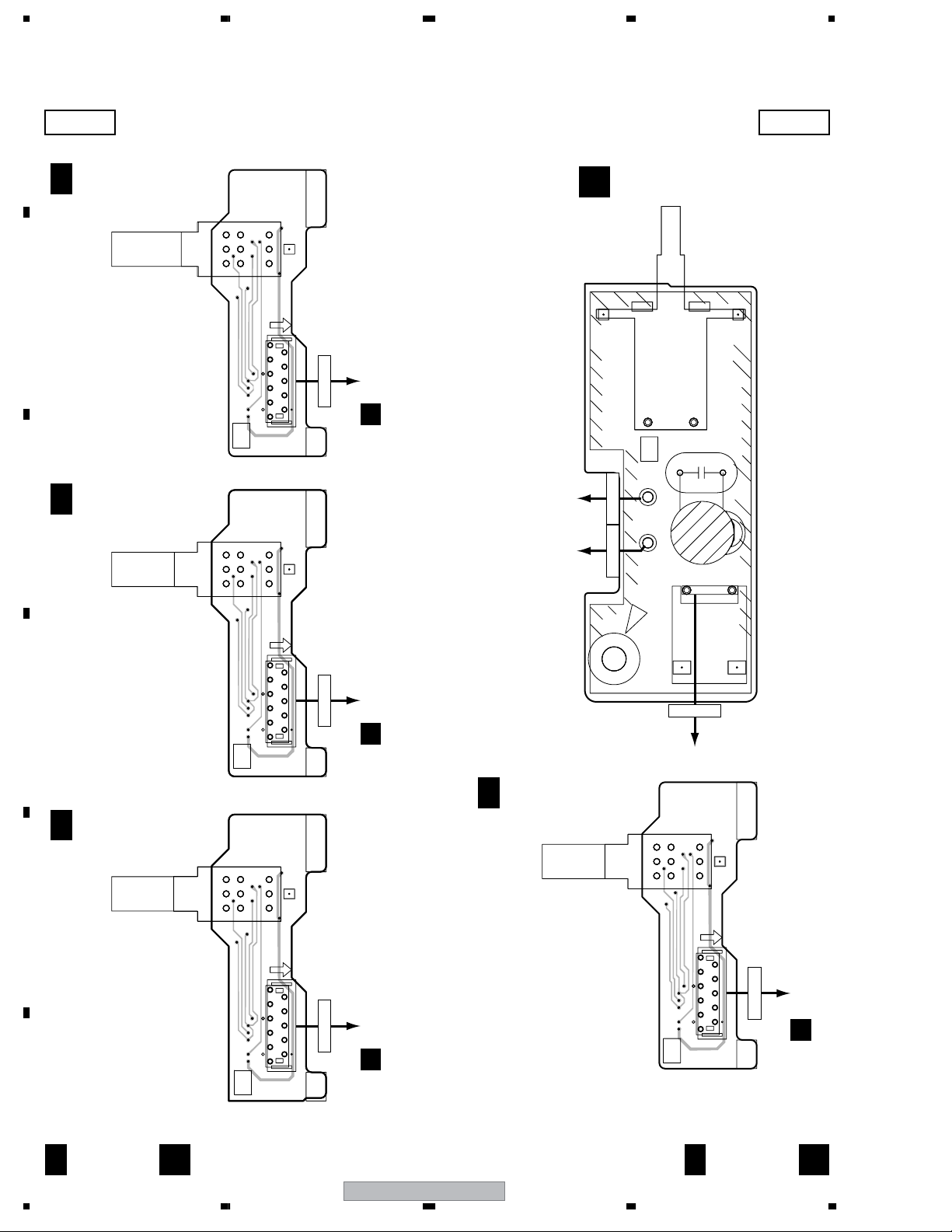
1234
4.3 TRIM 1 to TRIM 4 and ACSW ASSYS
A
SIDE A SIDE A
B
C
D 2/4
D 3/4
TRIM3 ASSY
TRIM2 ASSY
1
DWX2550- /J
11
LF
(DNP2208-C)
TRIM3
CN691
TRIM2
CN601
A
ACSW ASSY
R
ACSW
LIVE
LIVENEUTRAL
WHITE
BROWN
NEUTRAL
SW Power Supply
LF
NEUTRAL
2
C1
S1
PRIMARY
LIVE
1
D
E
F
D 4/4
TRIM1 ASSY
1
DWX2549- /J
11
LF
(DNP2208-C)
VR491 VR591 VR691
1
CN491 CN591 CN691
DWX2548- /J
11
LF
(DNP2208-C)
CN591
TRIM1
CN491
CN501
A
CN401
A
D 1/4
AC INLET ASSY
TRIM4 ASSY
CN91
DWX2545- /J
CN 91
VR791
1
CN791
DWX2551- /J
11
LF
(DNP2208-C)
(DNP2208-C)
TRIM4
CN791
CN701
A
D 1/4–4/4
92
1234
R
DJM-800
D 1/4–4/4
R
Page 93
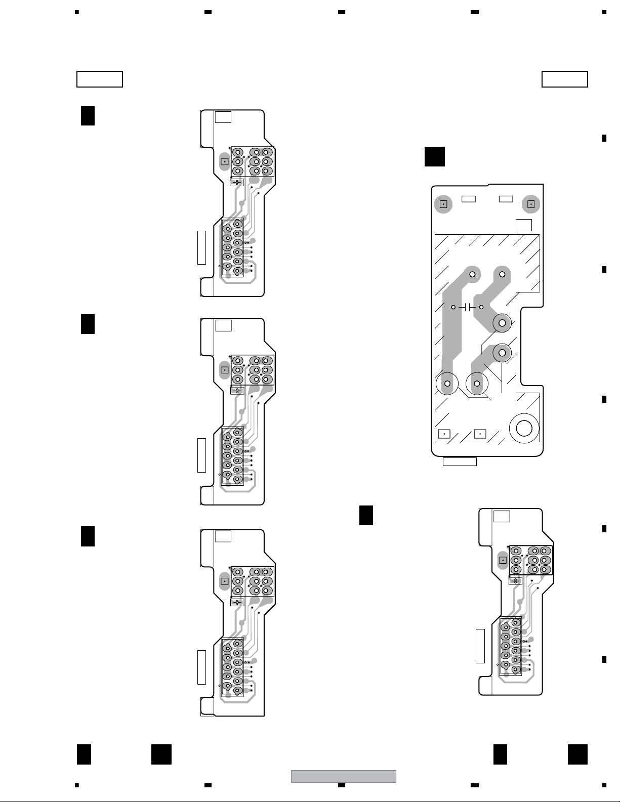
5678
SIDE B SIDE B
CN691CN591CN491
(DNP2208-C)
LF
LF
C691
TRIM3
ACSW ASSY
R
DWX2545- /J
ACSW
PRIMARY
LIVE
NEUTRAL
LF
D 2/4
D 3/4
TRIM3 ASSY
TRIM2 ASSY
A
B
C
D 4/4
TRIM1 ASSY
C591
TRIM2 TRIM1
(DNP2208-C)
LF
C491
111 111 111
D 1/4
LIVE
CN 91
TRIM4 ASSY
SOLDER
NEUTRAL
CN791
ADD
LF
C791
(DNP2208-C)
111
TRIM4
D
E
D 1/4–4/4
56
R
(DNP2208-C)
DJM-800
(DNP2208-C)
F
D 1/4–4/4
7
8
R
93
Page 94

1234
4.4 MIC1 and MIC2 ASSYS
A
SIDE A
SIDE A
MIC2 ASSY
E
DWX2543- /J
JA1501
MIC2
J1503
1
B
4
J1503
MIC2_0
1.
GNDA
2.
GNDA
3.
GNDA
4.
(DNP2207-C)
LF
JA1502
C
J1502
C1552
C1550
MIC1 ASSY
B
D1514
1
J1502
4
CN1503
45
C1504
R1509
C1516
C1534
IC1502
R1524
R1530
C1517
R1519
C1506
R1505
C1525
R1523
R1504
C1532
C1537
R1531
81
D1515
R1520
C1519
C1530
C1531
NP
NP
CN1501
C1535
1
15
V+5A
81
C1521
C1508
1
4
C1520
8
5
IC1503
C1507
R1503
C1538
MIC1 DWX2542
C1539
16
9
R1538
C1540
DSP_RESET3
24M
C1529
C1541
C1544
C1543
6M
C1542
V+15
D1519
C1549
D1520
8
V-15
D1518
1
C1551
D1521
IC1501
96K
1
12
CONTACT SIDE UP
V3R3
CN1502
CN1501
CN1503
(DNP2207-C)
IC1502 IC1503 IC1501
SIDE B SIDE B
CN456
A
CN1704
C
D
MIC1 ASSY
B
1
Q1503
2
R1522
C1522
R1521
Q1502
C1512
R1529
C1510
L1542
C1524
4
1
R1532
C1518
L1544
F1541
C1509
R1518
C1511
C1502
C1501
J1502
D1513
F1543
R1514
D1510
D1511
F1545
L1546
MIC1 DWX2542
F1549
C1547
4
E
CN1503 CN1501
7
R1540
5
6
C1548
C1528
C1546
5
F1548
F1547
C1527
LF
3
8
C1526
R1525
R1510
1
R1527
R1512
C1513
R1516
C1545
R1515
R1508
R1511
R1526
C1503
C1505
C1514
Q1504
R1517
Q1501
R1507
R1506
MIC2 ASSY
E
DWX2543- /J
LF
MIC2
1
J1503
4
D1512
C3 C2
2
3
C1
D1
1
MIC2_0
1.
2. GNDA
3.
GNDA
4.
GNDA
(DNP2207-C)
1
F
(DNP2207-C)
NOTE : The encircled numbers denote measuring point.
B E
94
B E
DJM-800
1234
Page 95

5678
4.5 CHFD1, CHFD2, CHFD3 and CHFD4 ASSYS
SIDE A SIDE B
CHFD1 ASSY
CHFD2 ASSY
1
4
CH1 FADER
LF
CN2601CN2604
DWX2537- /J
LF
CN2602CN2603
(DNP2207-C)
4
1
CN2602
YELLOW
VR205
CN1705
C
41
C
CN2602
CN2601
(DNP2207-C)
CN1706
CN2601
41
G 1/4
VR206
G 2/4
A
B
C
VR203
CN2603
41
CN1708
C
C
CN2603
(DNP2207-C)
(DNP2207-C)
CN1707
CN2604
(DNP2207-C)
YELLOW
41
G 3/4
G 4/4
VR204
CN2604
CHFD3 ASSY
CHFD4 ASSY
DWX2538- /JCH2 FADER
CH3 FADER DWX2539- /J
LF
CH4 FADER
1
4
DWX2540- /J
(DNP2207-C)
D
4
1
(DNP2207-C)
E
LF
(DNP2207-C)
G 1/4–4/4 G 1/4–4/4
56
DJM-800
7
8
95
F
Page 96

1234
C
C
4.6 PANEL 2 and DIGIA ASSYS
SIDE A
A
PANEL2 ASSY
F
LF
1/2
CRS FD CV
CH FD CV
BOOTH LEVEL
VR2102
B
S2114
S2113
103B-NON
142.0
MIC MONITOR
S2105
S2107
CUE MAS
D2137D2138
VR2101
V+5D
103B
MAS BALAN
DWX2554- /J
VR2104
PANEL2
S2110
D2133
D2134
C
S2109
EFFECT
ON/OFF
103B
LEVEL/DEPTH
TIME
2
4
5
3
1
EFFECT CH SEL
S2112
2
4
5
3
1
EFFECT SEL
S2111
D2135
D2136
S2106
TAP
S2108
CUE EF
D
DIGIA ASSY
L
DWX2555- /J DIGIA
DIG IN 4
JA1402
E
DIG IN 3
71
CN1401
(DNP2210-C)
1/2
DIG IN 1DIG IN 2
JA1401
CN1401
CN1201
K
F
F L
96
DJM-800
1234
Page 97

5678
D2137D2138
SIDE A
A
CN1711
C
CN2102
V+5D
CN2102
C2116
Lch
D2102
VR2101
103B
MAS BALANCE
D2135
D2136
S2106
TAP
S2108
CUE EFCT
C2115
AUTO/TAP
D2132
D2139
MIDI
START
S2104
S2103
Rch
D2117
DOWN
S2102
UP
D2103
D2118
S2101
D2104
D2119
30
D2105
D2120
D2121
D2106
39
D2122
D2107
D2108 D2109
D2123
34
C
D2124
CN1710
CN2101
CN2101
D2110
D2111
D2126
D2125
27
D2127
D2112
D2128
D2113
D2114
D2129
D2130
D2115
C2112
D2116
D2131
C2113
VR2103
103B-NON
MAS LEVEL
1
C2114
B
V2101
C
(DNP2210-C)
D
E
56
DJM-800
F
F
97
7
8
Page 98

A
2
2
SIDE B
1234
PANEL2 ASSY
F
CN2102CN2101
V+33
VF-
C2132
CONTACT SIDE
VF+
CN2101
27
1
30
V3R3REF
V3R3
1
CONTACT SIDE
CN2102
D2143
C2127
R2126
D2144
MUTE2
R2127
C2108
R2135
C2107
C2117
R2136
C2118
5
8
IC
41
R2120
D2148
IC
B
C2102
27
1
26.VF-
27.VF+
24.VF-
25.VF+
20.LED+4
21.LED+7
22.LED+10
23.LED+14
18.LED+1
19.LED+2
C
R2111
Q2102
16.LED-1
17.LED0
R2110
13.LED-5
14.LED-3
15.LED-2
R2112
Q2106
C2126
10.LED-15
11.LED-10
12.LED-7
C2136
Q2101
Q2101
3.FL_SO2
1.V+33
2.GNDM
4.FL_CK2
5.FL_LAT2
6.FL_BK2
7.LED04
8.LED05
9.LED-24
R2101
R2102
R2103
R2104
R2109
C2105
R2153
R2154
R2155
R2152
C2135
R2107
R2106
Q2105
C2125
R2105
14.LED_TAP
15.LED_EFON
16.SW_MAT7
13.LED_MASCUE
12.LED_EFCUE
29.GREF
30.V3R3REF
10.LED14
11.LED15
27.BEAT\EFON
28.GREF
26.EFFECT_PARA10
Q2105 Q2104Q2102 Q2103
34
C2133
C2134
7.VR_A01
8.MUTE2
9.TAP
5.VR_A03
6.VR_A02
20.SW_6
21.SW_5
22.SW_4
23.SW_3
24.SW_2
18.SW_MAT5
19.SW_MAT4
25.EFFECT_PARA11
C2104
R2108
1.GLED
2.V3R3
3.V+5D
4.VR_5
Q2104
17.SW_MAT6
D2101
Q2108
R2148
R2149
Q2108
39
D2141
C2119
R2150
R2118
R2117
Q2107
C2129
C2120
R2113
D2142
C2130
Q2103
Q2107Q2106
V+5D
C2121
C2122
D
E
F
98
F L
DIGIA ASSY
L
1/2
DWX2555- /J DIGIA
CN1401
1
7.DIGITAL_IN_4
1
CONTACT SIDE
7
7
LF
(DNP2210-C)
1.DIGITAL_IN_1
3.DIGITAL_IN_2
2.GNDD
4.GNDD
5.DIGITAL_IN_3
6.GNDD
CN1401
DJM-800
1234
Page 99
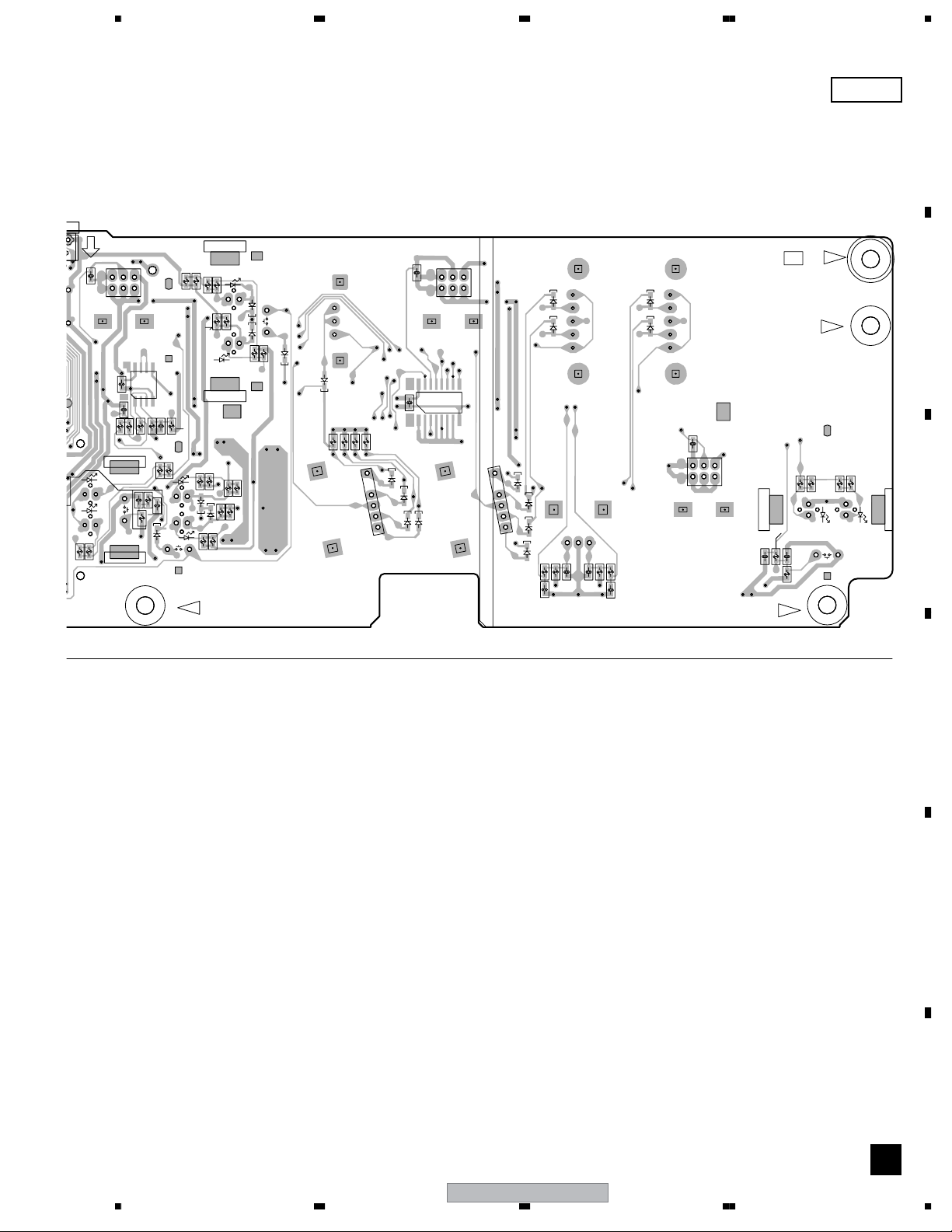
C2108
3
M
1
CN2102
R3
UTE2
R2135
CONTACT SIDE
C2107
8
C2118
C2117
R2136
5
41
R2120
IC2102
D2148
5678
SIDE B
A
R2162
R2119
R2151
R2158
R2163
R2146
D2160
R2159
R2144
R2129
R2132
R2147
R2125
R2131
C2131
R2128
D2161
R2130
R2145
R2156
R2157
R2134
R2160
R2161
D2162
D2163
R2133
D2149
D2145
R2115
R2137
R2114
R2116
S2111
1/2
C2106
IC2101
16
C2103
1
2
D2154
D2158
4
5
3
1
D2156
D2152
9
8
S2112
2
D2155
4
5
D2159
3
1
D2157
D2153
C2111
R2143
R2142
D2146 D2147
C2124
1
5
C2123
R2140
R2141
C2110
DWX2554- /J
1
D2150 D2151
5
C2101
PANEL2
C2109
R2138
LF
R2139
R2124
C2128
R2123
R2122
B
R2121
C
(DNP2210-C)
IC2101IC2102
D
E
56
DJM-800
F
F
99
7
8
Page 100

1234
3
C
R48
2
FK BL
C
F
N
N
4.7 DSP ASSY
SIDE A
A
B
C
D
IC47 IC48
IC43 IC44
E
IC39
IC12
IC22
IC5 IC6 IC7
IC11
IC45IC46
IC25
IC1
IC31
IC3
IC13
IC2
IC4
IC15
IC14
IC30
IC8
IC49
IC16
IC40
IC42
IC24
IC41
DSP ASSY
I
Q5
Q13
Q2
Q1
Q3
Q4
Q16
Q14
CN11
CN1502
B
KN4
CONTACT SIDE
14
IC5 IC6
C121
C217
C7
C218
CN14
1
R385
C135
C215
CN11
R386
IC2
TXD1
RXD1
1
V3R3
N.C.
MD
GNDD
6
12
1
R387
8
7
R383
16
1
6
R388
R384
R311
GNDD
R129
R128
C128
24M
D32
D33
D34
Q14
V3R3
R381
20
1
8
C3
CN1205
K
CN1
3
131
CONTACT SIDE
GNDD
V+5D
GNDD
RXD1
TXD1
MIDI_TX
C214
CN1
TXD6
GNDD
SCK6
RXD7
TXD7
SCK7
GNDD
RXD6
DIGIANA_SW1
DIGIANA_SW2
DIGIANA_SW3
DIGIANA_SW4
DSP DWX2534- /J
MCLK
GNDD
GNDD
SIO_SEL3
DSP_RESET3
SIO_SEL4
LF
R130
GNDD
MIC_DATA
GNDD
LRCK
GNDD
MCLK
GNDD
SCLK
GNDD
DSP_RESET3
GNDD
V3R3
R115
R116
R117
R118
11
C139
B
R382
R119
R194
R195
R196
R197
11
20
IC7
C129
10
1
6M
R373
R374
R375
R376
R377
R378
R198
10
96K
C216
R350
R349
C23
R177
R347
R239
R348
R179
R178
R78
R180
C152
C171
C172
C173
C169
C170
C191
C190
C189
C188
C187
C186
R355
R354
R11
R176
R175
R174
R173
R172
R218
R217
R216
R215
R214
R213
A
C140
36
37
CN1302
M
CONTACT SIDE
1
CN15
48/96_SW
SIO_SEL1
GNDD
GNDD
GNDD
RXD1
TXD1
C246
5
3131
R389
IC1
CN15
MASTER
C174
CN10
14
C157
C245
4
31
IC45
IC46
IC25
C22
2
10
DATA2
GNDD
24M
96K
GNDD
GNDD
6M
L4
C175
C39C4C40
Q5
D5
R7
R258
C46
R257
C47
R256
FPGA
RESET
R159
R158
R157
R156
R155
R154
R153
R152
R151
R150
R149
DSP_RESET
SCK2
1
144
GNDD
C176
C45
GNDD
C44
SCK1
7 8
R362
1
C156
R80
C148
R363
9
R364
IC3
R144
R212
R142
X1
R167
R165
R147
R163
R161
R145
20
C24
R143
11
IC24
72
73
R166
R141
14
8
R146
R148
C2
C1
IC8
8
7
R211
R210
R209
R208
R207
R206
R205
C183
R164
R15
R162
R160
10
C21
CN13
1
CPU
C18
R8
C20
R236
TXD2
R345
C16
C15
108
C17
C14
C251
D36
R395
IC49
R314
C250
CAUTION
REPLACE IC
LINKS AS
MARKED.MFD.BY
LITTELFUSE INC.
16
9
C221
1
8
R82
IC4
7
1
14
R81
14
C11
C204
D29
D30
D31
R183
GNDD
V3R3
LRCK
GNDD
GNDD
SCLK
DATA
SEND
SCK1
GNDD
MASTER_DATA2
C9
1
C42
C41
C43
R260
C48
C49
C51
C50
52
C52
C53
C54
C55C56
C60
C61
C62C63
C57 C58
C59
C130
Q13
A
C247
4315
5
4
13
IC47
C
A
C
4
DATA_REC
GNDD
MCLK
GNDD
1
CONTA
DSP_RESET2
C36
C243
C37
C38
208
53
R57
C66C67
C64 C65
C198
1
3
IC31
C91
R202
R203
B
C93
C131
R245
ATTENTION
REMPLACER LE
IC LINK COMME
INDEQUE.DE CHEZ
LITTELFUSE INC.
C143
DNP2
C35
C34
C8
R54
R55
R56
R226
5
R224
4
144
1
C92
36
37
R244
REC
C32
C
C
C33
R268
C31
DS
R50
R51
R52
R53
C90
C89
R225
C95
C94
R243
CPU_RESET
EFFECT_PARA10
EFFECT_PARA11
CH1_FADER
CH3_FADER
CH4_FADER
CRS_FADER
TAP
BEAT_EFON
VR_A01
VR_A02
VR_A03
GREF
GREF
VR0
VR1
VR2
VR3
VR4
VR5
DSP_RESET1
V+5D
V3R3
V+5D
V+5D
GLED
GLED
GLED
LED_DIG0
LED_DIG1
LED_DIG2
LED_CE1
LED_CE2
LED_CE3D0D1D2D3D4D5D6D7
KN1
CN6
1
1
CONTACT SIDE
SW_SCAN0
SW_SCAN1
SW_SCAN2
SW_MAT0
SW_MAT1
SW_MAT2
SW_MAT3
SW_MAT4
SW_MAT5
SW_MAT6
SW_MAT7
CH2_FADER
CN5
25
CN6
F
CN1703
C
V3R3REF
1
CONTACT SIDE
CN5
CN1702
C
MUTE2
30
I
100
1234
DJM-800
 Loading...