

Page 1
ORDER NO.
CRT3474
DEH-P70BT/EW
HIGH POWER CD/MP3/WMA PLAYER WITH BLUETOOTH WIRELESS TECHNOLOGY, RDS TUNER AND MULTI CD/DAB CONTROL
DEH-P70BT
This service manual should be used together with the following manual(s):
Model No. Order No. Mech.Module Remarks
CX-3158 CRT3394 S10.1AAC CD Mech. Module:Circuit Description, Mech. Description, Disassembly
/EW
For details, refer to "Important Check Points for Good Servicing".
PIONEER CORPORATION 4-1, Meguro 1-chome, Meguro-ku, Tokyo 153-8654, Japan
PIONEER ELECTRONICS (USA) INC. P.O. Box 1760, Long Beach, CA 90801-1760, U.S.A.
PIONEER EUROPE NV Haven 1087, Keetberglaan 1, 9120 Melsele, Belgium
PIONEER ELECTRONICS ASIACENTRE PTE. LTD. 253 Alexandra Road, #04-01, Singapore 159936
PIONEER CORPORATION 2005
K-ZZD.JUNE 2005 Printed in Japan
Page 2
1234
SAFETY INFORMATION
This service manual is intended for qualified service technicians; it is not meant for the casual do-it-yourselfer.
Qualified technicians have the necessary test equipment and tools, and have been trained to properly and safely
A
repair complex products such as those covered by this manual.
Improperly performed repairs can adversely affect the safety and reliability of the product and may void the warranty.
If you are not qualified to perform the repair of this product properly and safely, you should not risk trying to do so
and refer the repair to a qualified service technician.
Safety Precautions for those who Service this Unit.
• Follow the adjustment steps in the service manual when servicing this unit. When check-
ing or adjusting the emitting power of the laser diode exercise caution in order to get safe, reliable results.
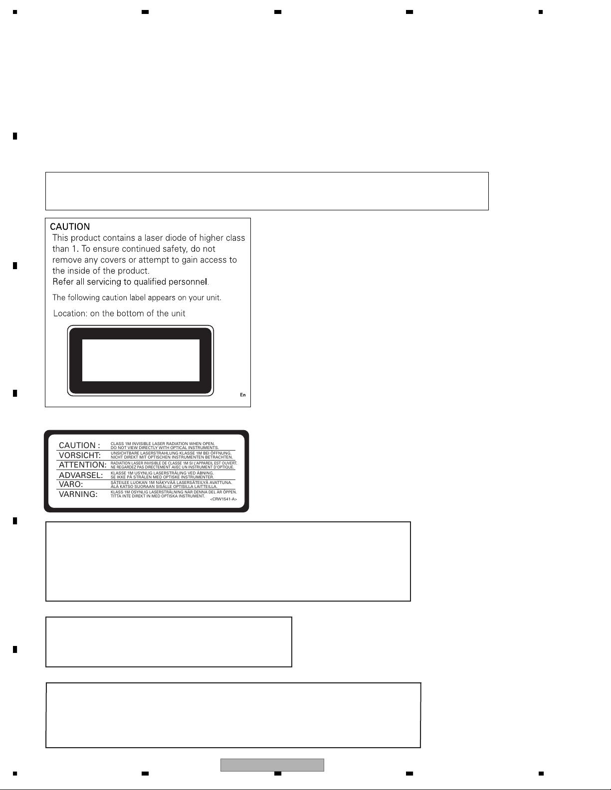
CAUTION:
B
USE OF CONTROLS OR ADJUSTMENTS OR PERFORMANCE OF PROCEDURES OTHER THAN THOSE
SPECIFIED HEREIN MAY RESULT IN HAZARDOUS RADIATION EXPOSURE.
C
CLASS 1
LASER PRODUCT
On the top of the player.
CAUTION :
D
VORSICHT:
ATTENTION:
ADVARSEL:
VARO:
VARNING:
The AEL (accessible emission level )of the laser power output is less than CLASS 1
but the laser component is capable of emitting radiation exceeding the limit for
CLASS 1.
E
A specially instructed person should do servicing operation of the apparatus.
CLASS 1M INVISIBLE LASER RADIATION WHEN OPEN.
DO NOT VIEW DIRECTLY WITH OPTICAL INSTRUMENTS.
UNSICHTBARE LASERSTRAHLUNG KLASSE 1M BEI ÖFFNUNG.
NICHT DIREKT MIT OPTISCHEN INSTRUMENTEN BETRACHTEN.
RADIATION LASER INVISIBLE DE CLASSE 1M SI L’APPAREIL EST OUVERT.
NE REGARDEZ PAS DIRECTEMENT AVECUN INSTRUMENT D’OPTIQUE.
KLASSE 1M USYNLIG LASERSTRÅLING VED ÅBNING.
SE IKKE PÅ STRÅLEN MED OPTISKE INSTRUMENTER.
SÄTEILEE LUOKAN 1M NÄKYVÄÄ LASERSÄTEILYÄ AVATTUNA.
ÄLÄ KATSO SUORAAN SISÄLLE OPTISILLA LAITTEILLA.
KLASS 1M OSYNLIG LASERSTRÅLNING NÄR DENNA DEL ÄR ÖPPEN.
TITTA INTE DIREKT IN MED OPTISKA INSTRUMENT.
<CRW1541-A>
WARNING!
Laser diode characteristics
Wave length : 785~814nm
Maximum output : 1190µW(Emitting period : unlimited)
Additional Laser Caution
F
Transistors Q101 in PCB drive the laser diodes.
When Q101 is shorted between their terminals, the laser diodes will radiate beam.
If the top cover is removed with no disc loaded while such short-circuit is continued,
the naked eyes may be exposed to the laser beam.
2
1234
DEH-P70BT/EW
Page 3
5678
CAUTION
Danger of explosion if battery is incorrectly replaced.
Replaced only with the same or equivalent type recommended by the manufacture.
Discord used batteries according to the manufacture's instructions.
- CD Section Precaution
1. You should conform to the regulations governing the product (safety, radio and noise, and other
regulations), and should keep the safety during servicing by following the safety instructions
described in this manual.
2. Before disassembling the unit, be sure to turn off the power. Unplugging and plugging the connectors
during power-on mode may damage the ICs inside the unit.
3. To protect the pickup unit from electrostatic discharge during servicing, take an appropriate treatment
(shorting-solder) by referring to "the DISASSEMBLY".
4. After replacing the pickup unit, be sure to check the grating.
A
B
C
D
E
56
DEH-P70BT/EW
F
7
8
3
Page 4
1234
[Important Check Points for Good Servicing]
In this manual, procedures that must be performed during repairs are marked with the below symbol.
Please be sure to confirm and follow these procedures.
A
B
C
D
1. Product safety
Please conform to product regulations (such as safety and radiation regulations), and maintain a safe servicing environment by
following the safety instructions described in this manual.
1 Use specified parts for repair.
Use genuine parts. Be sure to use important parts for safety.
2 Do not perform modifications without proper instructions.
Please follow the specified safety methods when modification(addition/change of parts) is required due to interferences such as
radio/TV interference and foreign noise.
3 Make sure the soldering of repaired locations is properly performed.
When you solder while repairing, please be sure that there are no cold solder and other debris.
Soldering should be finished with the proper quantity. (Refer to the example)
4 Make sure the screws are tightly fastened.
Please be sure that all screws are fastened, and that there are no loose screws.
5 Make sure each connectors are correctly inserted.
Please be sure that all connectors are inserted, and that there are no imperfect insertion.
6 Make sure the wiring cables are set to their original state.
Please replace the wiring and cables to the original state after repairs.
In addition, be sure that there are no pinched wires, etc.
7 Make sure screws and soldering scraps do not remain inside the product.
Please check that neither solder debris nor screws remain inside the product.
8 There should be no semi-broken wires, scratches, melting, etc. on the coating of the power cord.
Damaged power cords may lead to fire accidents, so please be sure that there are no damages.
If you find a damaged power cord, please exchange it with a suitable one.
9 There should be no spark traces or similar marks on the power plug.
When spark traces or similar marks are found on the power supply plug, please check the connection and advise on secure
connections and suitable usage. Please exchange the power cord if necessary.
0 Safe environment should be secured during servicing.
When you perform repairs, please pay attention to static electricity, furniture, household articles, etc. in order to prevent injuries.
Please pay attention to your surroundings and repair safely.
2. Adjustments
To keep the original performance of the products, optimum adjustments and confirmation of characteristics within specification.
Adjustments should be performed in accordance with the procedures/instructions described in this manual.
3. Lubricants, Glues, and Replacement parts
Use grease and adhesives that are equal to the specified substance.
E
Make sure the proper amount is applied.
4. Cleaning
For parts that require cleaning, such as optical pickups, tape deck heads, lenses and mirrors used in projection monitors, proper
cleaning should be performed to restore their performances.
5. Shipping mode and Shipping screws
To protect products from damages or failures during transit, the shipping mode should be set or the shipping screws should be
installed before shipment. Please be sure to follow this method especially if it is specified in this manual.
F
4
1234
DEH-P70BT/EW
Page 5

5678
CONTENTS
SAFETY INFORMATION......................................................................................................................................2
1. SPECIFICATIONS.............................................................................................................................................6
2. EXPLODED VIEWS AND PARTS LIST.............................................................................................................8
2.1 PACKING....................................................................................................................................................8
2.2 EXTERIOR(1)...........................................................................................................................................10
2.3 EXTERIOR(2)...........................................................................................................................................12
2.4 CD MECHANISM MODULE(S10.1AACA)................................................................................................14
3. BLOCK DIAGRAM AND SCHEMATIC DIAGRAM ..........................................................................................16
3.1 BLOCK DIAGRAM....................................................................................................................................16
3.2 OVERALL CONNECTION DIAGRAM(GUIDE PAGE)..............................................................................20
3.3 KEYBOARD UNIT ....................................................................................................................................26
3.4 CD MECHANISM MODULE(GUIDE PAGE).............................................................................................28
3.5 BLUETOOTH UNIT...................................................................................................................................38
4. PCB CONNECTION DIAGRAM ......................................................................................................................40
4.1 TUNER AMP UNIT ...................................................................................................................................40
4.2 KEYBOARD UNIT ....................................................................................................................................44
4.3 CD CORE UNIT(S10.1)............................................................................................................................46
4.4 PANEL UNIT.............................................................................................................................................48
4.5 ANTENNA PCB ........................................................................................................................................49
4.6 BLUETOOTH PCB....................................................................................................................................50
5. ELECTRICAL PARTS LIST .............................................................................................................................52
6. ADJUSTMENT ................................................................................................................................................60
6.1 DISPLAY TEST MODE.............................................................................................................................60
6.2 CD ADJUSTMENT ...................................................................................................................................62
6.3 CHECKING THE GRATING AFTER CHANGING THE PICKUP UNIT.....................................................64
6.4 ERROR MODE.........................................................................................................................................66
6.5 BLUETOOTH TEST MODE ......................................................................................................................67
6.6 OEL UNIT ADJUSTMENT........................................................................................................................72
6.7 SYSTEM MICROCOMPUTER TEST PROGRAM....................................................................................73
7. GENERAL INFORMATION .............................................................................................................................74
7.1 DIAGNOSIS..............................................................................................................................................74
7.1.1 DISASSEMBLY ......................................................................................................................................74
7.1.2 CONNECTOR FUNCTION DESCRIPTION ..........................................................................................79
7.2 IC ..............................................................................................................................................................80
7.3 OPERATIONAL FLOW CHART................................................................................................................93
8. OPERATIONS .................................................................................................................................................94
A
B
C
D
E
F
56
DEH-P70BT/EW
7
8
5
Page 6
1234
1. SPECIFICATIONS
A
B
C
D
E
F
6
1234
DEH-P70BT/EW
Page 7
5678
A
B
C
D
E
56
DEH-P70BT/EW
F
7
8
7
Page 8
N
1234
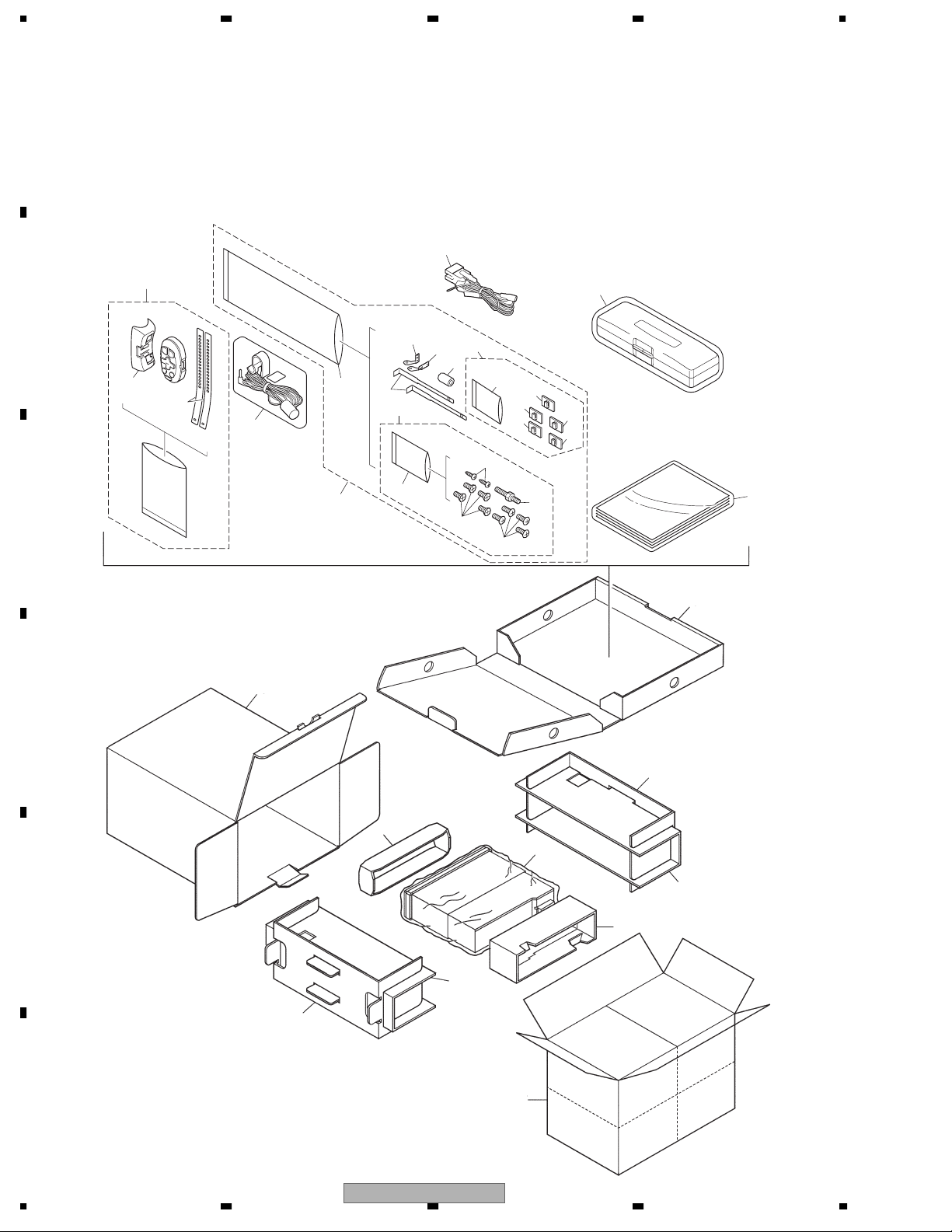
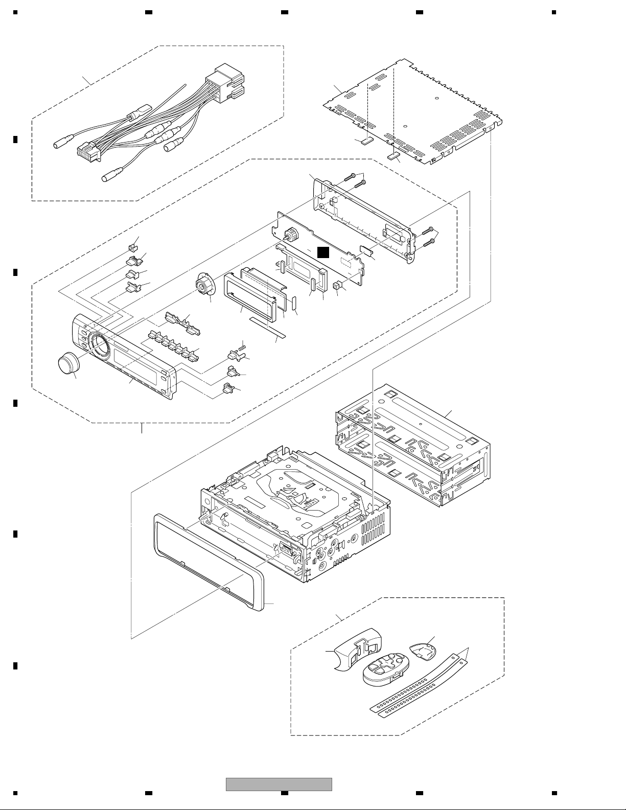
2. EXPLODED VIEWS AND PARTS LIST
OTES : • Parts marked by " * " are generally unavailable because they are not in our Master Spare Parts List.
• The > mark found on some component parts indicatesthe importance of the safety factor of the part.
A
Therefore, when replacing, be sure to use parts of identical designation.
• Screw adjacent to mark on the product are used for disassembly.
• For the applying amount of lobricants or glue, follow the instructions in this manual.
(In the case of no amount instructions,apply as you think it appropriate.)
2.1 PACKING
"
1
23
B
14
25
24
20
C
18
D
11
12
5
2
8
13
15
3
4
17
17
17
6
7
9
10
22
17
17
21
30
26
28
16
27
E
27
26
F
8
1234
DEH-P70BT/EW
19
29
Page 9
5678
PACKING SECTION PARTS LIST
Mark No. Description Part No.
1 Cord Assy CDE7153
2 Accessory Assy CEA4862
3 Cord Clamper Assy CEA4636
* 4 Polyethylene Bag E36-615
5 Screw Assy CEA5317
6 Screw BPZ20P060FTB
7 Screw CBA1650
* 8 Polyethylene Bag CEG-127
9 Screw CRZ50P090FTC
10 Screw TRZ50P080FTC
* 11 Polyethylene Bag CEG-158
12 Handle CNC5395
13 Holder CND1250
14 Holder CND2699
15 Bush CNV3930
16 Polyethylene Bag CEG-162
* 17 Clamper CNV8262
18 Carton CHG5647
19 Contain Box CHL5647
Mark No. Description Part No.
20 Microphone Assy CPM1059
21-1 Polyethylene Bag CEG1116
21-2 Owner's Manual CRD3985
21-3 Owner's Manual CRD3986
21-4 Owner's Manual CRD4041
21-5 Installation Manual CRD4042
* 21-6 Caution Card CRP1207
* 21-7 Passport CRY1013
* 21-8 Warranty Card CRY1157
22 Case Assy CXB3520
23 Remote Control Assy CXC4293
24 Belt CZN5499
25 Holder CZN7041
26 Protector CHP2383
27 Protector CHP2384
28 Protector CHP2432
29 Protector CHP2555
30 Sub Carton CHA3167
A
B
Owner's Manual,Installation Manual
Part No. Language
CRD3985 English, Spanish
CRD3986 German, French
CRD4041 Italian, Dutch
CRD4042 English, Spanish, German, French, Italian, Dutch
C
D
E
56
DEH-P70BT/EW
F
7
8
9
Page 10
1234
2.2 EXTERIOR(1)
27
1
13
5
24
6
7
22
23
10
20
26
15
16
19
17
11
8
9
12
15
B
18
2
34
34
4
14
31
32
4
21
A
B
C
3
D
E
F
30
28
29
25
33
10
1234
DEH-P70BT/EW
Page 11

5678
EXTERIOR(1) SECTION PARTS LIST
Mark No. Description Part No.
1 Cord Assy CDE7153
2 Case CNB3160
3 Detach Grille Assy CXC4291
4 Screw BPZ20P100FTB
5 Button(PHONE) CAC9098
6 Button(LIST) CAC9099
7 Button(ATT) CAC9100
8 Button(EQ) CAC9101
9 Button(DISP) CAC9102
10 Button(1-6,TA) CAC9103
A
11 Button(OPEN) CAC9123
12 Cover CNS8208
13 Lighting Conductor CNV8435
14 Connector(CN1501) CKS5207
15 Cushion CNM6633
16 Spacer CNM7697
17 Spacer CNM7698
18 Holder CNV6910
19 OEL Unit MXS8221
20 Holder XNC7006
21 Cushion XNM7049
22 Holder XNV7023
23 Button Unit(SRC-BAND) CXC4357
24 Sub Grille Unit CXC4397
25 Belt CZN5499
26 Spring XBH7001
27 Knob Unit XXA7337
28 Remote Control Assy CXC4293
29 Battery Cover CZN5497
30 Panel XNS7089
31 Holder CNC8659
32 IC(IC1562) TSOP4840SB1
33 Holder CZN7041
34 Sheet CNM9600
B
C
D
56
DEH-P70BT/EW
E
F
7
8
11
Page 12
1234
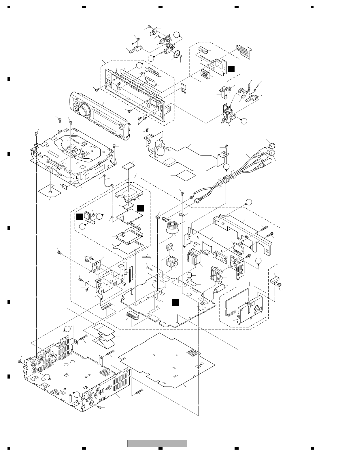
2.3 EXTERIOR(2)
52
55
A
74
62
51
2
11
2
82
43
F
3
19
19
8
B
A
8
42
15
34
B
2
C
84
D
45
46
56
76
47
29
62
2
59
75
A
79
62
2
14
18
44
E
41
22
35
57
52
60 80
B
58
78
77
13
40
31
22
26
A
C
83
30
27
50
54
48
10
49
61
53
70
25
36
23
68
72
33
71
66
D
65
E
38
20
63
67
17
17
21
21
F
12
9
64
69
D
73
2
F
6
37
7
24
32
28
E
E
4
1
C
D
F
12
1234
5
4
16
81
1
4
DEH-P70BT/EW
39
Page 13

>
5678
EXTERIOR(2) SECTION PARTS LIST
Mark No. Description Part No.
1 Screw BMZ30P040FTB
2 Screw BSZ26P060FTC
3 Screw BSZ30P060FTC
4 Screw BSZ30P200FTC
5 Cable CDE7842
6 Cord Assy CDE7843
7 IC(IC351) PAL007B
8 Transistor(Q551,751) 2SD2396
9 Earth Plate CNC8915
10 Shield CND2791
11 Insulator CNM7682
12 Cushion CNM8890
13 Insulator CNM9597
14 Sheet CNM9599
15 IC(IC911) NJM2388F84
16 Insulator CNM9628
17 Cap CNV6727
18 Tuner Amp Unit CWM9941
19 Screw ASZ26P060FTC
20 Screw BPZ26P080FTC
21 Screw BSZ26P160FTC
22 Clamper CEF1047
23 Fuse(10A) CEK1208
24 Pin Jack(CN301) CKB1051
25 Plug(CN981) CKM1376
26 Plug(CN302) CKS1238
27 Connector(CN101) CKS3408
28 Plug(CN801) CKS3537
29 Connector(CN701) CKS3837
30 Connector(CN151) CKS4124
31 Connector(CN971) CKS4977
32 Antenna Jack(CN401) CKX1056
33 Holder CND2700
34 Holder CND2701
35 Insulator CNM9629
36 Sheet CNM9265
37 Heat Sink CNR1668
38 FM/AM Tuner Unit CWE1801
39 Holder CND2144
40 Bluetooth Unit CWM9942
Mark No. Description Part No.
50 Insulator XNM7031
51 Detach Grille Assy CXC4291
52 Screw(M2x4) CBA1649
53 Microphone(MIC251) CPM1068
54 Washer CBF1038
55 Spring CBH2650
56 Cord Assy CDE7847
57 Earth Plate CND2708
58 Gear CNV5997
59 Arm CNV7400
60 Damper Unit CXB9503
61 Button(EJECT) CAC7752
62 Screw CBA1925
63 Spring CBH2651
64 Spring CBH2652
65 Spring CBH2653
66 Holder CND1254
67 Arm CNV7401
68 Arm CNV7402
69 Arm CNV7403
70 Panel Unit CWM8758
71 Connector(CN1951) CKS4806
72 Connector(CN1950) CKS5192
73 Holder Unit CXB9502
74 Sub Panel Unit CXC4398
75 Cover CNM6854
76 Panel CNS8209
77 Lighting Conductor CNV6487
78 Spring CBL1512
79 Pin CNV6486
80 Holder Unit CXC4388
81 Chassis Unit CXC4387
82
83 Screw ISS26P055FTC
84 Insulator XNM7106
CD Mechanism Module(S10.1AACA)
CXK5668
A
B
C
D
E
41 Connector(CN1051) CKS4244
42 Connector(ANT1001) CKS5058
43 Connector(ANT1102) CKS5058
44 Holder CND2703
45 Holder CND2704
46 Insulator CNM9449
47 Sheet CNM9598
48 Choke Coil(L981) CTH1280
49 Terminal(CN402) VNF1084
56
DEH-P70BT/EW
F
7
8
13
Page 14
1234
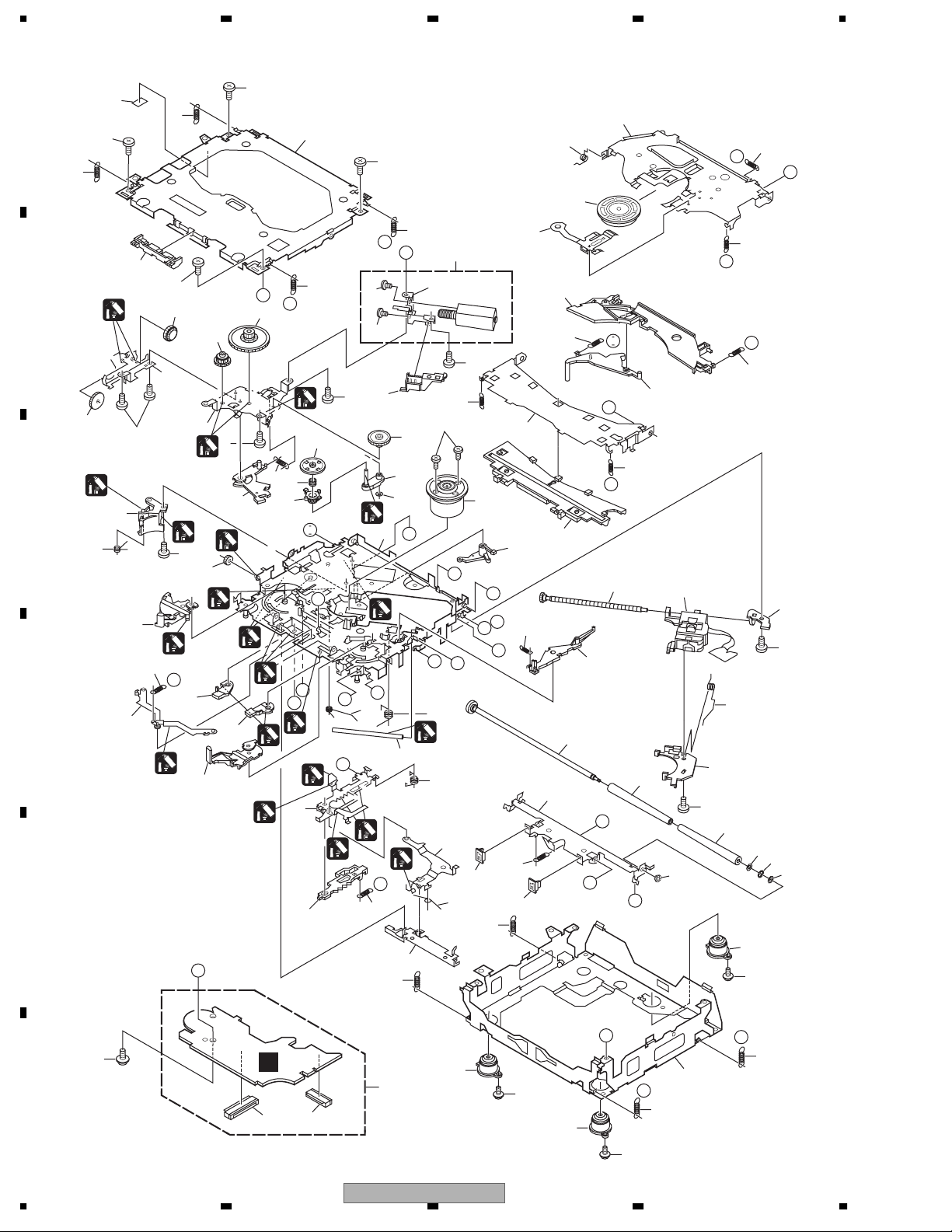
2.4 CD MECHANISM MODULE(S10.1AACA)
A
13
5
13
42
5
81
34
5
15
22
E
F
93
13
A
B
44
5
B
1
54
52
53
13
C
D
86
86
82
83
4
37
71
4
29
51
1
73
50
72
10
1
I
76
55
5
36
4
1
18
2
C
24
47
7
64
2
1
61
2
M
1
23
87
75
B
E
63
57
62
58
1
G
L
1
N
R
1
1
2
40
1
56
D
O
16
P
33
1
1
P
19
J
12
3
20
39
1
69
30
2
21
M
D
79
2
1GEM1024
2GEM1045
3GEM1035
E
92
26
G
68
28
I
H
28
45
J
38
23
K
59
49
F
Q
A
27
H
77
90
48
8
67
17
78
25
70
60
80
N
L
K
43
46
6
60
11
89
10
14
74
R
31
41
85
C
91
F
C
3
65
1
2
85
66
35
O
31
Q
14
85
14
1234
DEH-P70BT/EW
Page 15

5678
CD MECHANISM MODULE(S10.1AACA) SECTION PARTS LIST
Mark No. Description Part No.
1 CD Core Unit(S10.1) CWX3096
2 Connector(CN101) CKS4182
3 Connector(CN901) CKS4017
4 Screw BMZ20P035FTC
5 Screw BSZ20P040FTC
6 Screw(M2x4) CBA1362
7 Screw(M2x3) CBA1824
8 Screw(M2x3) CBA1825
9 •••••
10 Washer CBF1038
11 Washer CBF1060
12 Spring CBH2390
13 Spring CBH2606
14 Spring CBH2607
15 Spring CBH2608
16 Spring CBH2609
17 Spring CBH2610
18 Spring CBH2735
19 Spring CBH2612
20 Spring CBH2613
21 Spring CBH2614
22 Spring CBH2615
23 Spring CBH2616
24 Spring CBH2617
25 Spring CBH2620
26 Spring CBH2621
27 Spring CBH2641
28 Spring CBH2642
29 Spring CBH2643
30 Spring CBH2659
31 Spring CBH2688
32 •••••
33 Shaft CLA4441
34 Frame CNC9962
35 Frame CNC9963
36 Bracket CND2712
37 Bracket CND1895
38 Arm CNC9968
39 Arm CND1909
40 Lever CND2032
41 Lever CNC9984
42 Sheet CNM8134
43 Collar CNV7798
44 Guide CNV7799
45 Arm CNV8403
Mark No. Description Part No.
50 Gear CNV8379
51 Gear CNV8380
52 Gear CNV8381
53 Gear CNV8382
54 Gear CNV8383
55 Gear CNV8384
56 Rack CNV8385
57 Arm CNV8386
58 Arm CNV8387
59 Guide CNV8388
60 Roller CNV7218
61 Gear CNV8389
62 Arm CNV8391
63 Arm CNV8390
64 Arm CNV8392
65 Damper CNV7313
66 Damper CNV7314
67 Arm CNV8394
68 Arm CNV8395
69 Guide CNV8396
70 Guide CNV8397
71 Holder CNV8398
72 Arm CNV8402
73 Gear CNV8400
74 Damper CNV7618
75 Motor Unit(M1) CXC4440
76 Chassis Unit CXC2318
77 Screw Unit CXB8729
78 Gear Unit CXC2397
79 Arm Unit CXC2316
80 Arm CND1896
81 Arm CND1894
82 Motor Unit(M2) CXB8933
83 Bracket CNC9985
84 •••••
85 Screw(M2x5) EBA1028
86 Screw JFZ20P020FTC
87 Screw JGZ17P022FTC
88 •••••
89 Washer YE20FTC
90 Pickup Unit(P10)(Service) CXX1641
91 Screw IMS26P030FTC
92 Spring CBL1635
93 Clamper CNV8372
A
B
C
D
E
46 Rack CNV8374
47 Holder CNV8376
48 Holder CNV8377
49 Arm CNV8378
56
DEH-P70BT/EW
F
7
8
15
Page 16
N
X
D
C
M
C
3
8
1234
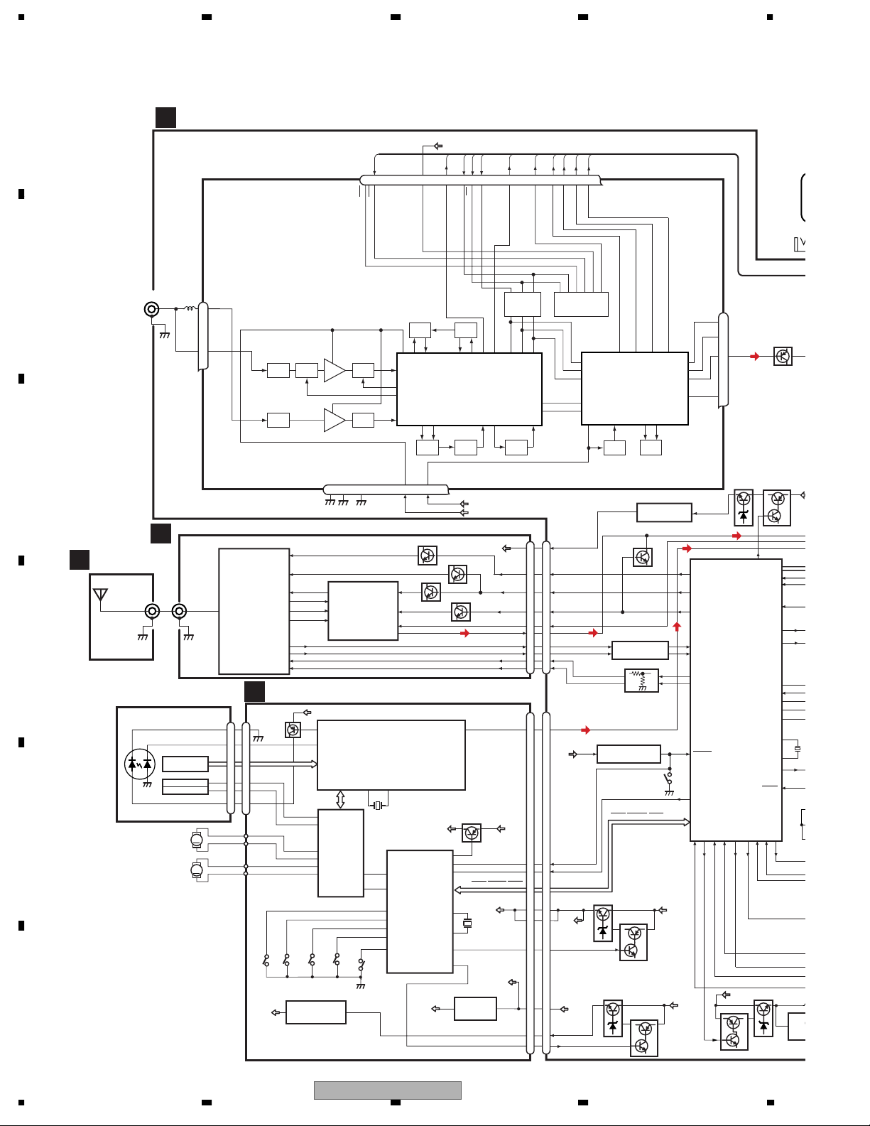
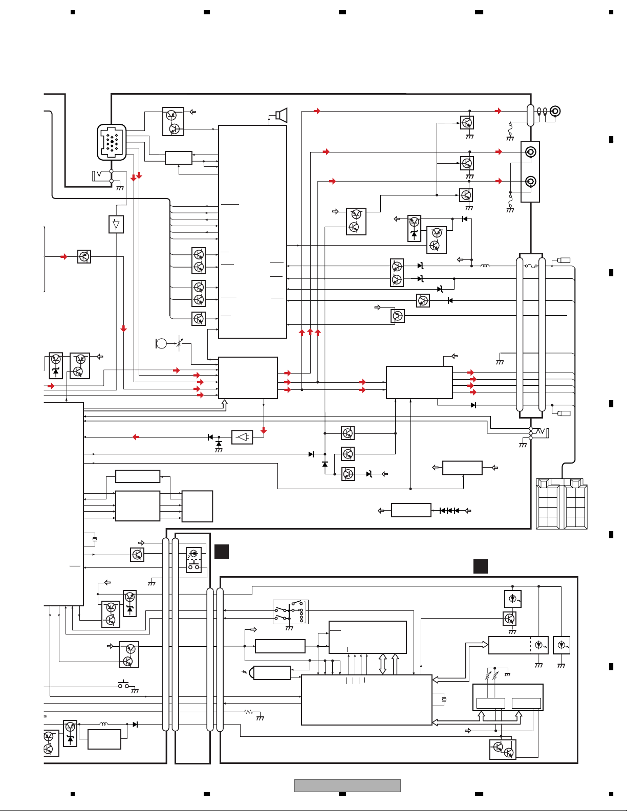
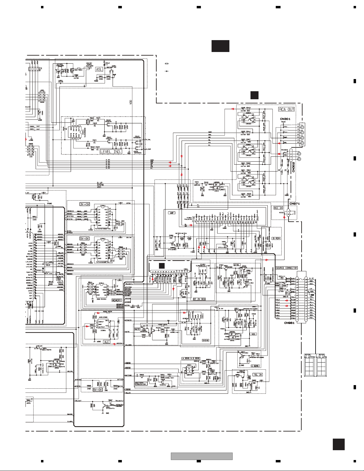
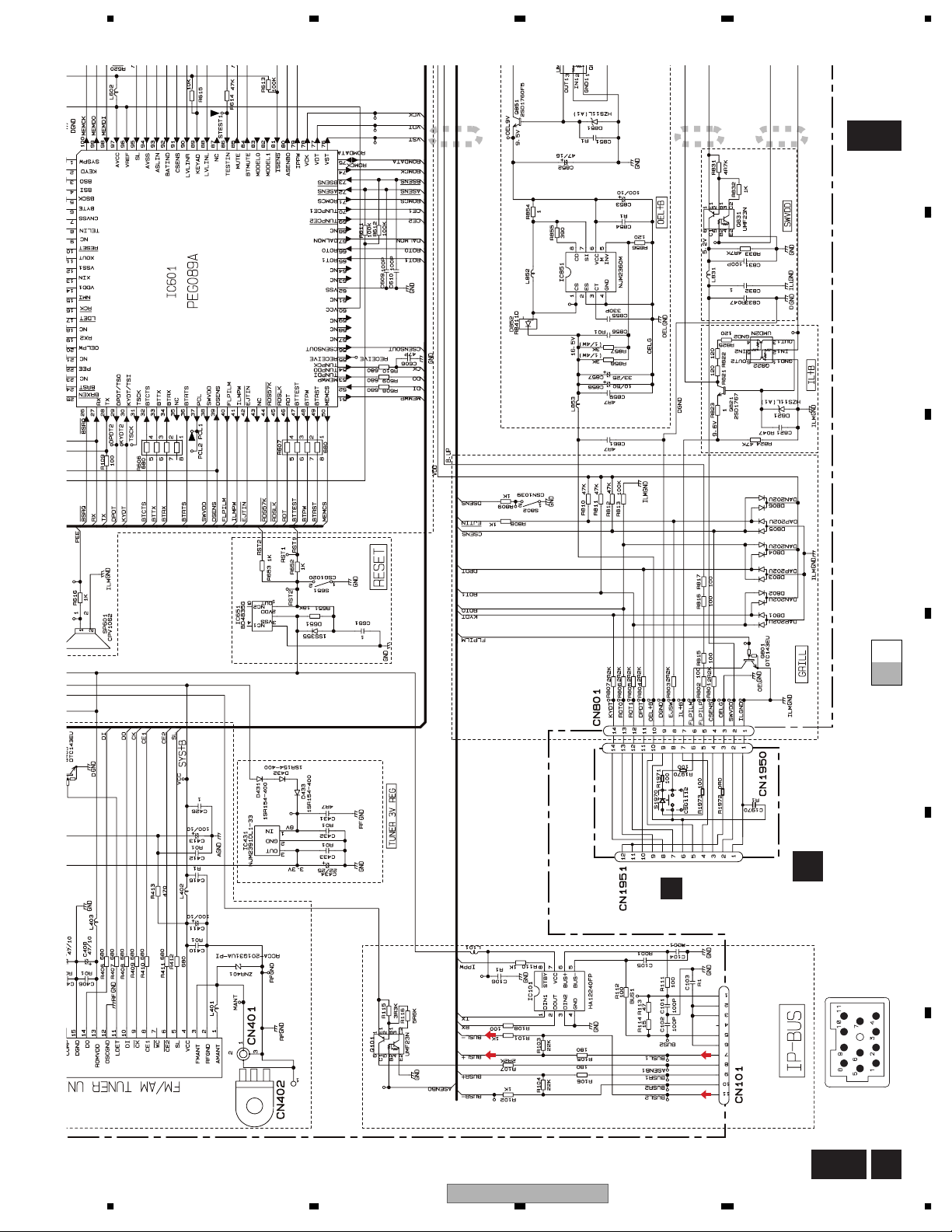
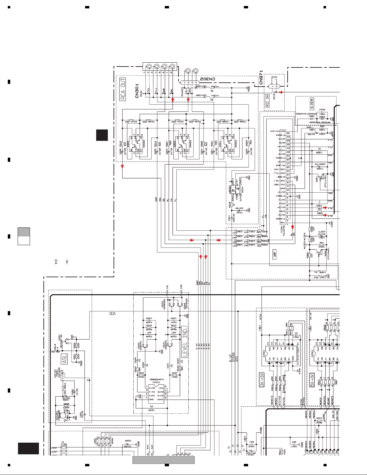
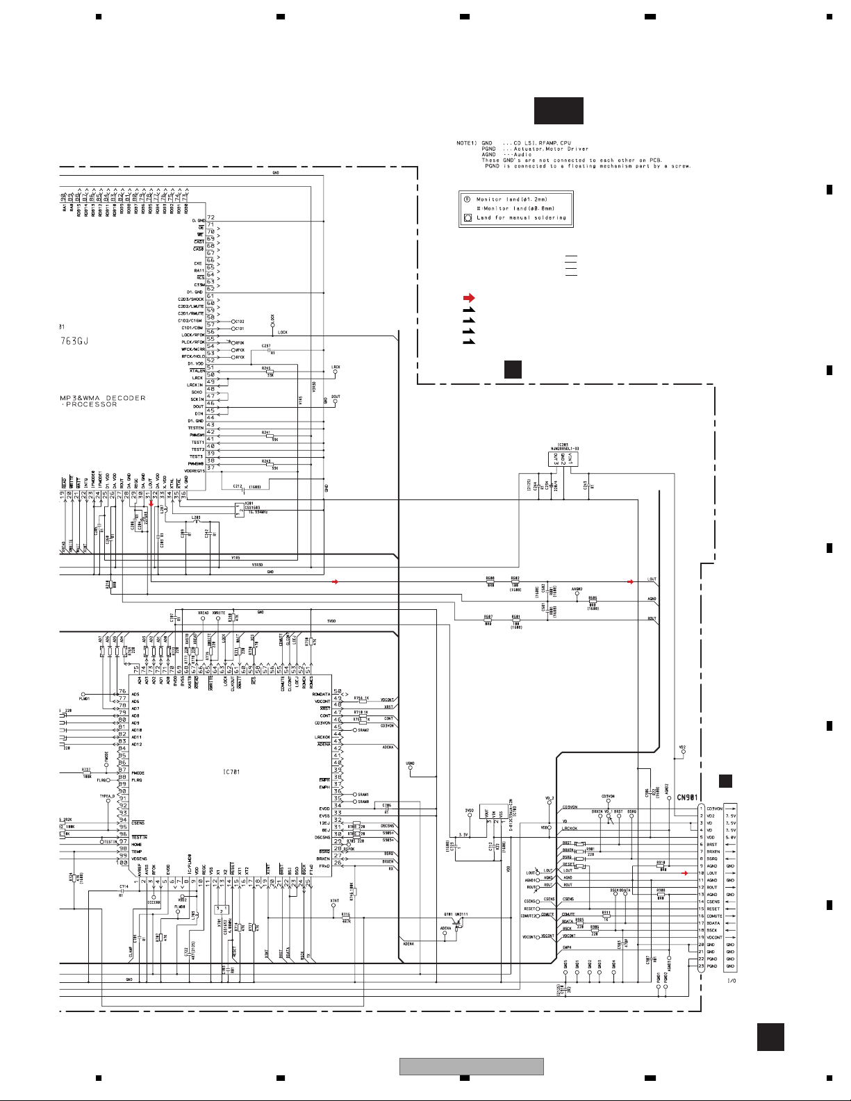
3. BLOCK DIAGRAM AND SCHEMATIC DIAGRAM
3.1 BLOCK DIAGRAM
A
TUNER AMP UNIT
A
VDD
FM/AM TUNER UNIT
SL
CK
CE2
7 13 5 10 8 11 14 18 19 20 21
69
WC
CE2
ROM_VDD
DO
CE1
DI
SL
CK
CE1
LDET
LDET
DI
DO
RDSCK
RDSLOCK
RDSDATA
IP-BUS
RDSHSLK
C
MIC IN
B
C
D
E
F
BLUETOOTH
ANTENNA
16
FM/AM ANTENNA
ANTENNA PCB
F
ANT1101
CN401
1
3
BLUETOOTH PCB
E
ANT1102
PICKUP UNIT
(P10)(SERVICE)
LASER
DIODE
MONITOR
DIODE
LOAD/
ANT1001
1
2,3
HOLOGRAM
UNIT
FOCUS ACT.
TRACKING ACT.
SPINDLE
MOTOR
CARRIAGE
MOTOR
AM ANT
1
FM ANT
3
BLUETOOTH MODULE
Y1001
CWX3131
A5
RF_I/O
LD-
15
MD
5
FO+
1
TO+
4
LD+
14
M
M
ATT
ATT
P1
SIOF_SS2
Q2
RESETP
N2
SIOF_RXD
N1
SIOF_SCK
N3
SIOF_TXD
SIOF_SYNC
I2
SCIF1_RTS
H3
SCIF1_TXD
H2
SCIF1_RXD
I1
SCIF1_CTS
CD CORE UNIT(S10.1)
C
F,E
12EJ
SENSE
SENSE
3
NJM2885DL1-33
V3R3D
142
143
12
13
16
15
18
17
8EJ
IC203
LD
PD
TD/FD
FOP
TOP
SOP
SOM
LCOP
LCOM
15
5
1
4
14
CN101
FOP
TOP
CLAMP
SENSE
V3R3D
Q101
AC,BD
+3.3V REGULATOR
TANK
RFTANK
LPF
RF
RFGND
OSCGND
DGND
VCC
212 15 4 17
2
DX
3
BCLK
4
DR
5O2
FS
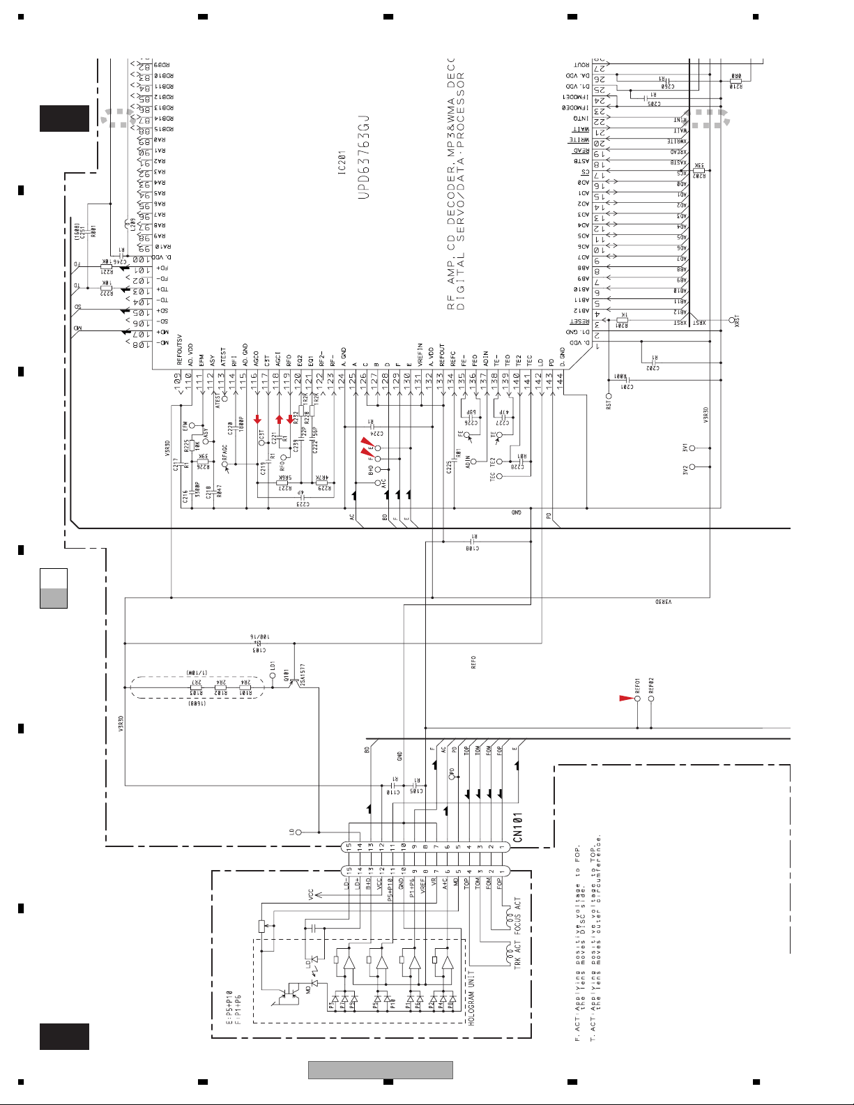
DIGITAL SERVO / DATA PROCESSOR
DRIVER
IC301
BA5835FM
DISC
SENSE
RSTN
CODEC
MUTEN
IC1041
VFTN
AK2301A
IC201
UPD63763GJ
RF-AMP,CD DECODER,
MP3 , WMA, DECODER,
SD/MD
X201
CD
53
22
LOEJ
9
47
CONT
4
32
31
30
97
HOME
2
VD2
VDD_3.3
Q1001
Q1041
22
23
15
7
GSR
3534
A/D REF
CSENSE
LOEJ
IC701
CONT
PE5454B
CD CONTROLLER
CLAMP
12EJ
8EJ
DSCSNS
HOME
VDCONT
CD3VON
3VDD
ADENA
RESET
DEH-P70BT/EW
LPFVCO
IC1
MIX/IF/PLL
TUN 3.3V
SYS +B
CN1051
3.3V
Q1002
Q1042
31
LOUT
Q701
43
14
94
BRST,BRXEN,BSRQ
BDATA,BSCK
VD
12
X1
X701
13
X2
49
46
+3.3V REGULATOR
3
VDD
IC703
S-812C33AUA-C2N
IC4
5V 3.3V
X-talCFIFT
BT3V
BTTEST
BTRST
BTMUTE
MICIN
TELOUT
BTCTS
BTRX
BTTX
BTRTS
CN901
L-OUT
VDD
VDCONT
2
VD2
CD3VON
VD
IC3
←
EEPROM
IC2
DET/NC/MPC/MPX/DIV/RDS
OSC
REG
BT3V REGULATOR
3
IC451
NJM2391DL1-33
1414
BTTEST
77
BTRST
88
BTMUTE
12
12
MICIN
1010
TELOUT1
11
BTCTS3
3
3
BTRX3
5
5
4
4
6
6
CN701
CDL
10
14
VDD
RESET
15
9
CSENS
14
10
VD
3
21
20
4
VD
VDCONT
5
19
19
5
VD2
22
2
CD3VON
23
1
MUTE
Q591
3V -> 5V
4
IC501(2/2)
98
TC74VHCT08AFTS1
2
BRST,BRXEN,BSRQ
Q751
Q753
5V -> 3V
RESET
IC651
BD4835G
BDATA,BSCK
MECHA VD
Q752
MECHA VD
Q754
S651
RESET
BTTX3
BTRTS3
VDD
6
1
24,25,26,
3,4,5
B.UP
47
49
84
32
34
33
36
10
56
VD
1
BTTEST
BTRST
BTMUTE
BTCTS
BTRX
BTTX
BTRTS
RESET
CSENSOUT
91
COMP
16
Rch
24
Lch
23
ANT1
22
SYSTEM
CONTROLLER
IC601(2/2)
PEG089A
KYDT/TSI
DSENS
CSENS
OELPW
20
30
39
Q852
OELPW
Q551
29
B.UP
BTPW
MEMWP
SWVDD
DPDT/TSO
38
65
DEEMPHASIS
Q401
Q552
Q553
48
KEYAD
KEYD
LVLINL
MUTE
SYSPW
MEMCS
MEMDI
MEMDO
MEMCK
XIN
XOUT
FLPILM
EJTIN
ILMPW
ROT166ROT0
41
Q851
6,7
DC-DC
1234
AN612
89
2
88
85
1
50
98
51
99
100
13
11
40
42
AL
IC5
15
V
I
NJ
Page 17
T
Q
5678
A
22
SYSTEM
CONTROLLER
IC601(1/2)
PEG089A
PreoutL
IC201
FrontoutL
PML009A
RearoutL
SELoutL
1
IC241
57
9.6V
Phase B
Phase A
SWVDD
3.3V REGULATOR
5,4
S-818A33AUC-BGN
IC1562
TSOP4840SB1
REMOTE CONTROL
SENSOR
SP601
BUZZER
PEE
67
DALMON
73
BSENS
72
ASENS
92
BATIND
81
ISENS
8
TELIN
12
10
11
MULTI-CONTROL
S1501
10
1
IC1551
3
1
RL
SWL
FL
MUTING
B.UP
Q304
VDD REGULATOR
Q901
VDD
Q902
BACKUP SENSE
Q921
ACC SENSE
VDD
Q951
Q941
ILM SENSE
Q302
SWL
Q303
Q301
B.UP
TELEPHONE MUTE
B.UP
6,20
23
OUT4-
21
OUT4+
3
OUT2-
5
OUT2+
25
SYS+B REGULATOR
2
IC911
NJM2388F84
4
1
1
SYS +B
Q352
Q351
Q381
E-MUTE
MUTE
TUN 3.3V
14
12
MUTE
POWER AMP
IN4(FL)
IN2(RL)
22
B.UP
SYSPW
TUNER 3.3V
REGULATOR
3
NJM2391DL1-33
IC351
PAL007B
STBYMUTE
4
IC431
Switch_out
SYS+B
B
JOYST
33
3.3V
23
1
60
14
96
5
REM
Vdd1
Vdd2
27
DPDT
28
KYDT
ROM
BYTE/VPP
IC1563
PD8140A
VCC
97
Vref
RD
CE
CS2
CS1
2
12
14
43
42
46
47
48
RD
CS1
CS0
CS2
AVcc
KEY/OEL CONTROLLER
IC1561
PEG088A
DATA
ADDRESS
VR1592
95
92
KD1-4,KS1-4
JOYST
BTLED
13
Xout
Xin
11
16MHz
CKA,CKC,CKD,
D1_L,D0_L,LS
SWVDD
X1561
OTL +TAB OTL -TAB
5.2V
16.5V
Q1591
8.7V REGULATOR
6
Q101
IC101
HA12240FP
8
CE2
CE1
DO
DI
CK
SL
RDSCK
RDSLOCK
RDSDATA
RDSHSLK
LDET
VR251
1
2
3
5
6
CN1950
6
8
9
7
2
11
14
4
B.UP
1
TX
RX
2
IPPW
Q404
Q403
Q405
VST,VCK,VDT
MEMORY
IC541
S99-50084
CS
SO
W#
SI
SCK
S1970
CN1951
80
ASENBO
28
TX
19
RX2
27
RX
79
IPPW
69
TUNPCE2
70
TUNPCE1
53
TUNPDO
52
TUNPDI
54
TUNPCK
95
SL
16
RCK
45
RDSLK
46
RDT
44
RDS57K
17
LDET
93
ASLIN
ELECTRONIC VOLUME/
SOURCE SELECTOR
15
NoiseDETout
13
MIcin
40
IN1L
43
IN4+L
44
IN4-L
42
IN3L
41
IN2L
NJM4558MD
LEVEL INDICATOR
PANEL UNIT
D
CN1501
IL+B
4
4
ROT0
9
9
ROT1
7
7
SWVDD
2
2
OPT IN
DPDT
10
10
KYDT
8
8
CSENS
3
3
OEL+B
5
5
CN101
8
5
IP-BUS
MIC IN
CN971
ALC
IC581
AN6123MS
1
7
11
BUSL-
BUSL+
IP-BUS DRIVER
BUS-
BUS+
5
6
3
5
DEEMPHASIS
Q401
MIC251
Q552
Q551
48
BTPW
KEYAD
KEYD
LVLINL
MUTE
SYSPW
MEMCS
MEMDI
MEMWP
MEMDO
EM
MEMCK
OLLER
1(2/2)
XIN
089A
DPDT/TSO
29
38
FLPILM
SWVDD
65
XOUT
EJTIN
ROT166ROT0
41
Q553
85
1
50
98
51
99
100
13
11
40
42
ILMPW
89
2
88
15.000MHz
B.UP
KEYAD
KEYD
3
1
4
12
9
X601
ILB CONTROL
B.UP
Q822
VDD
BUSL+
BUSLTUNL
CDL
3V -> 5V
IC501(2/2)
TC74VHCT08AFTS1
5V -> 3V
IC521
TC74VHC08FTS1
CN801
B.UP
FLDILM
Q801
Q821
Q831
SWVDD
EJSW
IL+B
ROT0
ROT1
1
3
6
11
8
565
8
9
7
13 13
12 12
2
DSENSE
S802
DPDT
11
KYDT
14
CSENS
B.UP
Q851
852
6,7
DC-DC CONVERTER
IC851
NJM2360M
1
OEL+B
4
10 10
CN302
RL
FL
FUSE
3A
FUSE
3A
CN981
BUP1
ACC1
GND1
RL22
BRE1
B.UP
ILL1
TEL1
FL22
FL21
RL21
CN301
8
7
4
3
16
14
12
15
11
CN151
2
1
FUSE
16
10A
14
12
9
9
15
7
7
5
5
8
8
6
6
11
3
2
1
WIRED
REMOTE
CONTROL
BACK
UP
ILM
GND
KEYBOARD UNIT
BT-IND-ILM
Q1501
KEY MATRIX
S1531-S1544
VR1591
OEL UNIT
7
10
ILLUMINATION
Q1592
2,8
5
8.7V
4,16
REAR L
FRONT L
NON-FAD OR
SUB WOOFER L
BACK UP
ACC
ILM
TELMUTE
GND
FLFL+
RL-
RL+
B.REM
RR
RR
+
FR
FR
+
-
B.
FL
FL
REM
+
-
RL
RL
ACC
+
-
B
C
D
E
F
56
DEH-P70BT/EW
7
8
17
Page 18
1234
- Current Block Diagram
A
B
C
D
E
SYSPW
B.UP CWE1801
Source OFF
BT standby
430
437
399
BT measurement
468
472
430
BT immobile
252
259
223
Backup current
2.842
2.842
2.450
[mA]
SYS +B
VDD
BTPW
BT 5V 212
VDCOUNT
OELPW
D/D CON
ILMPW
ILL +B
243.68
243.68
243.68
TUN 3.3
66.45
66.45
66.45
SWVDD
214
214
214
Mecha rush
FF/REV
2.12 (A)
611
2.07 (A)
601
1.89 (A)
592
Dimmer OFF
Dimmer ON
52.92/ 76.24
51.58/ 62.90
52.60/ 75.79
51.27/ 62.59
54.61/ 78.49
53.25/ 64.51
70.36
68.33
61.13
121.21
121.21
121.21
17.235
17.235
17.201
VDD 3.3
BT 3V
0.233
0.233
0.233
212
212
133
133
133
7.039/ 2.761
7.017/ 2.273
7.032/ 2.765
7.016/ 2.282
7.039/ 2.750
7.019/ 2.266
TUNER VCC
E-VOL PML009A
LEVEL IND NJM4558MD
TUNER VDD 3.3 CWE1801
SYSTEM µ- COM PEG089A
CWE1801TUNER ROM_VDD
CXK5668CD VDD
HA12240FPIP-BUS
ROM CORRECTION
BD4835GRESET IC
GRILL µ- COM PEG089ASW VDD
REMOTE IC
P-BLUE OEL+VE TAB
P-BLUE OEL-VE TAB
PEG088AGRILL µ-COM
PD8140AROM
BT-MODULE CWX3131
CODEC
HF MICAMP AN6123MS
CD VD CXK5668VD
CD VD 2 CXK5668VD 2
DC/ DC IC
OEL +VE TAB
OEL -VE TAB-VE +B
KEY ILL Bule 11mA × 11 121mA
EJ SW ILL CSG1112EJ ILL
AK2301A
S99-50084FLASH 1Mbit
TC74VHC08FTS1 (×2)5V ⇒ 3V IC
TC74VHCT08AFTS13V ⇒ 5V IC
P-BLUE OEL
NJM2360M
P-BLUE OEL
F
18
1234
DEH-P70BT/EW
Page 19
5678
- Voltage Block Diagram
SYSPW
B.UP CWE1801
Voltage set
value
14.4
15.1
(excessive)
10.8
(decrease)
[V]
SYS +B
VDD
BTPW
BT 5V 3.254
8.42
8.42
8.42
5.24
5.24
5.23
5.22
5.25
5.18
TUN 3.3
SWVDD
3.329
3.329
3.328
5.15
5.16
5.13
VDD 3.3
BT 3V
3.328
3.328
3.327
3.254
3.252
TUNER VCC
CAPTAIN 4 PML009A
LEVEL IND NJM4558MD
TUNER VDD 3.3 CWE1801
SYSTEM µ- COM PEG089A
CWE1801TUNER ROM_VDD
CXK5668CD VDD
HA12240FPIP-BUS
ROM CORRECTION
BD4835GRESET IC
GRILL µ- COM PEG089ASW VDD
REMOTE IC
P-BLUE OEL+VE TAB
P-BLUE OEL-VE TAB
PEG088AGRILL µ-COM
PD8140AROM
BT-MODUL CWX3131
CODEC
AK2301A
S99-50084FLASH 1Mbit
TC74VHC08FTS1 (×2)5V ⇒ 3V IC
A
B
C
VDCOUNT
OELPW
D/D CON
ILMPW
ILL +B
8.123
8.123
7.989
Black/Blue
9.47/ 9.46
9.54/ 9.53
9.28/ 9.27
9.41
9.57
9.16
5.51
5.51
5.51
8.71
8.71
8.71
HF MICAMP AN6123MS
TC74VHCT08AFTS13V ⇒ 5V IC
CD VD CXK5668VD
CD VD 2 CXK5668VD 2
DC/ DC IC
OEL +VE TAB
OEL -VE TAB-VE +B
KEY ILL Bule 11mA × 11 121mA
EJ SW ILL CSG1112EJ ILL
NJM2360M
P-BLUE OEL
P-BLUE OEL
D
E
56
DEH-P70BT/EW
F
7
8
19
Page 20
1234
3.2 OVERALL CONNECTION DIAGRAM(GUIDE PAGE)
Note: When ordering service parts, be sure to refer to " EXPLODED VIEWS AND PARTS LIST" or
"ELECTRICAL PARTS LIST".
A
A-a
Large size
A-a A-b
SCH diagram
A-a
A-b
Guide page
A-a
B
Detailed page
A-b
FM(100%):-15.5dBs
AM(30%):-26.0dBs
C
CN901
CD:0dBs
ELECTRONIC VOLUME,
SOURCE SELECTOR
C
NOT USED
D
RESET
E
B
CN1501
IB-BUS:+2.2dBs
F
PANEL UNIT
D
EJECT
BSENSE
SYSTEM CONTROL
A D
20
1234
DEH-P70BT/EW
Page 21
5678
A
A-b
NOTE :
Symbol indicates a resistor.
No differentiation is made between chip resistors and
discrete resistors.
Symbol indicates a capacitor.
No differentiation is made between chip capacitors and
discrete capacitors.
The > mark found on some component parts indicates
the importance of the safety factor of the part.
Therefore, when replacing, be sure to use parts of
identical designation.
Decimal points for resistor
and capacitor fixed values
are expressed as :
←
2.2 2R2
←
0.022 R022
TUNER AMP UNIT
A
FRONT
OUTPUT
SUB WOOFER,
NON FADING
OUTPUT
REAR
OUTPUT
B
FM:+7.6dBs
AM:-0.9dBs
IB-BUS:10.3dBs
CD:10.1dBs
TEL:+11.1dBs
TEL:-5dBs
E
CN1051
POWER AMP
>>
FM:+33.6dBs
AM:+25.1dBs
IP-BUS:+36.3dBs
CD:+36.1dBs
TEL:+37.1dBs
MICROPHONE
INPUT
>
FUSE
CEK1208
10A
BACK
UP
B.
ILM
REM
ACC
GND
C
D
E
RR
RR
+
FR
FR
+
FL
FL
+
RL
RL
+
-
56
DEH-P70BT/EW
F
A
7
8
21
Page 22
A
B
A-b
1234
1
ELECTRONIC VOLUME,
SOURCE SELECTOR
C
NOT USED
A-b
A-a
A-a
D
E
CD:0dBs
F
A-a
22
CN901
C
FM(100%):-15.5dBs
AM(30%):-26.0dBs
1234
DEH-P70BT/EW
Page 23
5678
A
3 42
SYSTEM CONTROL
A-b
B
RESET
BSENSE
EJECT
B
CN1501
PANEL UNIT
D
A-b
A-a
A-a
C
D
E
56
DEH-P70BT/EW
IB-BUS:+2.2dBs
F
A-a
7
8
D
23
Page 24
1234
A
SUB WOOFER,
NON FADING
OUTPUT
OUTPUT
REAR
OUTPUT
MICROPHONE
INPUT
FRONT
>>
B
TUNER AMP UNIT
A
←
←
Decimal points for resistor
and capacitor fixed values
are expressed as :
2.2 2R2
0.022 R022
C
A-b
A-a
Symbol indicates a resistor.
No differentiation is made between chip resistors and
discrete resistors.
Symbol indicates a capacitor.
No differentiation is made between chip capacitors and
discrete capacitors.
The > mark found on some component parts indicates
the importance of the safety factor of the part.
Therefore, when replacing, be sure to use parts of
NOTE :
identical designation.
D
POWER AMP
E
F
A-b
24
FM:+7.6dBs
AM:-0.9dBs
IB-BUS:10.3dBs
CD:10.1dBs
TEL:+11.1dBs
1
DEH-P70BT/EW
1234
Page 25
5678
+
+
+
+
RL
FL
FR
>
FUSE
CEK1208
RR
-
RR
10A
FM:+33.6dBs
AM:+25.1dBs
IP-BUS:+36.3dBs
CD:+36.1dBs
TEL:+37.1dBs
FR
BACK
-
-
-
RL
FL
B.
REM
ACC
UP
GND
ILM
A
B
CN1051
E
C
A-b
A-a
D
TEL:-5dBs
E
56
DEH-P70BT/EW
F
3 42
7
8
A-b
25
Page 26
1234
3.3 KEYBOARD UNIT
A
CN1951
D
B
MULTI- CONTROL
C
D
E
F
B
26
1234
DEH-P70BT/EW
Page 27
5678
A
KEYBOARD UNIT
B
B
C
D
E
56
DEH-P70BT/EW
F
B
7
8
27
Page 28
1234
Y
3.4 CD MECHANISM MODULE(GUIDE PAGE)
A
PICKUP UNIT(P10)(SERVICE)
B
C-a
F
T
C
S
%
F
T
F
T
T
F
F
T
F
F
T
T
#
@
C
D
3
2
1
E
M1 CXC4440
SPINDLE MOTOR
M2 CXB8933
LOADING
/CARRIAGE
MOTOR
S
S
C
C
T
9
F
0
F
F
T
T
CD DRIVER
$
S
7
C
8
4
5
S
C
S
C
T
F
C
28
1234
DEH-P70BT/EW
Page 29
5678
A
C-b
SWITCHES:
CD CORE UNIT(S10.1)
ras
!
S901:HOME SWITCH..........ON-OFF
S903:DSCSNS SWITCH......ON-OFF
S904:12EJ SWITCH.............ON-OFF
S905:8EJ SWITCH...............ON-OFF
The underlined indicates the switch position.
SIGNAL LINE
F
FOCUS SERVO LINE
T
TRACKING SERVO LINE
C
CARRIAGE SERVO LINE
S
SPINDLE SERVO LINE
CD CORE UNIT(S10.1)
C
B
TYPE_A/D
MICRO COMPUTER
PE5454B
SRAMLEVEL2
SRAMLEVEL1
SRAMLEVEL0
3V REGULATOR
3.3V REGULATOR
C
D
A
CN701
6
E
^
&
DEH-P70BT/EW
56
F
C
7
8
29
Page 30
A
C-b
1234
1
2
B
C
C-b
A-a
C-a
F
T
C
S
#
@
%
T
T
F
F
D
E
F
C-a
30
T
T
F
F
T
TFF
PICKUP UNIT(P10)(SERVICE)
DEH-P70BT/EW
1234
Page 31

5678
A
2
3 4
5 6
C-b
B
4
C-b
A-a
C-a
C
7
$
S
8
C
C
5
C
S
S
CD DRIVER
D
F
T
F
9
T
0
F
T
E
2
3
1
S
S
M1 CXC4440
SPINDLE MOTOR
C
DEH-P70BT/EW
56
C
LOADING
/CARRIAGE
M2 CXB8933
7
MOTOR
8
F
C-a
31
Page 32

1234
A
B
CD CORE UNIT(S10.1)
3.3V REGULATOR
C
SIGNAL LINE
FOCUS SERVO LINE
TRACKING SERVO LINE
CARRIAGE SERVO LINE
C
SWITCHES:
CD CORE UNIT(S10.1)
S901:HOME SWITCH..........ON-OFF
S903:DSCSNS SWITCH......ON-OFF
S904:12EJ SWITCH.............ON-OFF
S905:8EJ SWITCH...............ON-OFF
C-b
C-a
D
F
The underlined indicates the switch position.
SPINDLE SERVO LINE
T
S
C
E
F
C-b
32
!
ras
1
2
DEH-P70BT/EW
1234
Page 33

5678
A
CN701
3V REGULATOR
A
6
B
^
&
C
SRAMLEVEL2
MICRO COMPUTER
SRAMLEVEL0
SRAMLEVEL1
PE5454B
C-b
C-a
D
E
TYPE_A/D
F
2
3 4
DEH-P70BT/EW
56
5 6
7
8
C-b
33
Page 34

1234
- Waveforms Note : 1. The encircled numbers denote measuring points in the circuit diagram.
2. Reference voltage REFO1(1.65V)
A
1 DSCSNS
2 8SNS
3 12SNS
4 LOEJ
12 cm CD Loading operation
5V/div
5V/div
5V/div
5V/div
500ms/div
1 DSCSNS
5 CLCONT
4 LOEJ
6 VD
12 cm CD Loading operation 8 cm CD Loading operation
5V/div
5V/div
5V/div
10V/div
500ms/div
1 DSCSNS
2 8SNS
3 12SNS
4 LOEJ
5V/div
5V/div
5V/div
5V/div
500ms/div
Ref.:
GND
Mode:
Normal
B
7 SIN
8 CIN
9 TIN
12 cm CD-DA setup operation after loading 12 cm CD-ROM(3 sessions) setup operation
Ref.:
C
REFO
Mode:
Normal
0 FIN
! RFOK
7 SIN
12 cm CD-DA Source On setup operation
D
1V/div
500mV/div
500mV/div
200mV/div
2V/div
2V/div
2s/div
500ms/div
Ref.:
GND
Mode:
Normal
7 SIN
8 CIN
9 TIN
12 cm CD-ROM(1 session) setup operation
after loading
Ref.:
REFO
Mode:
Normal
@ TE
# FE
Source On setup operation CD-DA Play operation
1V/div
500mV/div
500mV/div
500mV/div
500mV/div
1s/div
200ms/div
Ref.:
GND
Mode:
Normal
7 SIN
8 CIN
9 TIN
after loading
Ref.:
REFO
Mode:
Normal
# FE
0 FIN
@ TE
9 TIN
1V/div
500mV/div
500mV/div
500mV/div
500mV/div
500mV/div
500mV/div
2s/div
20ms/div
Ref.:
REFO
Mode:
Normal
# FE
0 FIN
E
@ TE
9 TIN
CD-ROM play operation(Regular track Jump)
Ref.:
REFO
Mode:
Normal
F
34
500mV/div
500mV/div
500mV/div
500mV/div
1234
20ms/div
Ref.:
REFO
Mode:
Normal
$ MDX
7 SIN
Spindle waveform during play operation Spindle waveform during play operation
Ref.:
REFO
Mode:
Normal
1V/div
200mV/div
50ms/div
Ref.:
REFO
Mode:
Normal
$ MDX
7 SIN
(Wider)
Ref.:
REFO
Mode:
Normal
2V/div
1V/div
5µs/div
DEH-P70BT/EW
Page 35

5678
0 FIN
# FE
Focus Search waveform
Ref.:
REFO
Mode:
TEST
% RFAGC
@ TE
9 TIN
4 Tracks Jump waveform 32 Tracks Jump waveform
Ref.:
REFO
Mode:
TEST
500mV/div
500mV/div
1V/div
500mV/div
500mV/div
200ms/div
500µs/div
@ TE
% RFAGC
500mV/div
500mV/div
2ms/div
% RFAGC
@ TE
9 TIN
Track Open waveform 1 Track Jump waveform
Ref.:
REFO
Mode:
TEST
% RFAGC
@ TE
9 TIN
10 Tracks Jump waveform
Ref.:
REFO
Mode:
TEST
1V/div
500mV/div
500mV/div
1ms/div
Ref.:
REFO
Mode:
TEST
% RFAGC
@ TE
9 TIN
Ref.:
REFO
Mode:
TEST
1V/div
500mV/div
500mV/div
1V/div
500mV/div
500mV/div
500µs/div
A
B
2ms/div
C
% RFAGC
@ TE
8 CIN
7 SIN
Search operation(Outter to Inner)
Ref.:
REFO
Mode:
Normal
1 DSCSNS
5 CLCONT
4 LOEJ
12 cm CD Eject operation
Ref.:
GND
Mode:
Normal
1V/div
1V/div
500mV/div
2V/div
5V/div
5V/div
5V/div
200ms/div
500ms/div
^ LOUT
& ROUT
Analog audio waveform
Ref.:
AGND
Mode:
Normal
1 DSCSNS
2 8SNS
3 12SNS
4 LOEJ
8 cm CD Eject operation
Ref.:
GND
Mode:
Normal
1V/div
1V/div
5V/div
5V/div
5V/div
5V/div
200µs/div
500ms/div
1 DSCSNS
2 8SNS
3 12SNS
4 LOEJ
12 cm CD Eject operation
Ref.:
GND
Mode:
Normal
7 SIN
8 CIN
9 TIN
CD-DA >> CD-ROM mode change(Band key)
Ref.:
REFO
Mode:
Normal
5V/div
5V/div
5V/div
5V/div
1V/div
500mV/div
500mV/div
500ms/div
500ms/div
D
E
56
DEH-P70BT/EW
F
7
8
35
Page 36

1234
7 SIN
8 CIN
A
9 TIN
CD-ROM >> CD-DA mode change(Band key)
Ref.:
REFO
Mode:
Normal
B
C
1V/div
500mV/div
500mV/div
500ms/div
% RFAGC
9 TIN
@ TE
0 FIN
Black dot(800µm) during play
Ref.:
REFO
Mode:
Normal
1V/div
1V/div
1V/div
1V/div
500µs/div
D
E
F
36
1234
DEH-P70BT/EW
Page 37

5678
A
B
C
D
E
56
DEH-P70BT/EW
F
7
8
37
Page 38

1234
3.5 BLUETOOTH UNIT
A
BLUETOOTH PCB
E
B
C
D
E
ANTENNA PCB
F
F
E
F
38
1234
DEH-P70BT/EW
Page 39

5678
A
A
B
BLUETOOTH UNIT
Consists of
BLUETOOTH PCB
ANTENNA PCB
C
D
E
56
DEH-P70BT/EW
F
E
7
8
39
Page 40

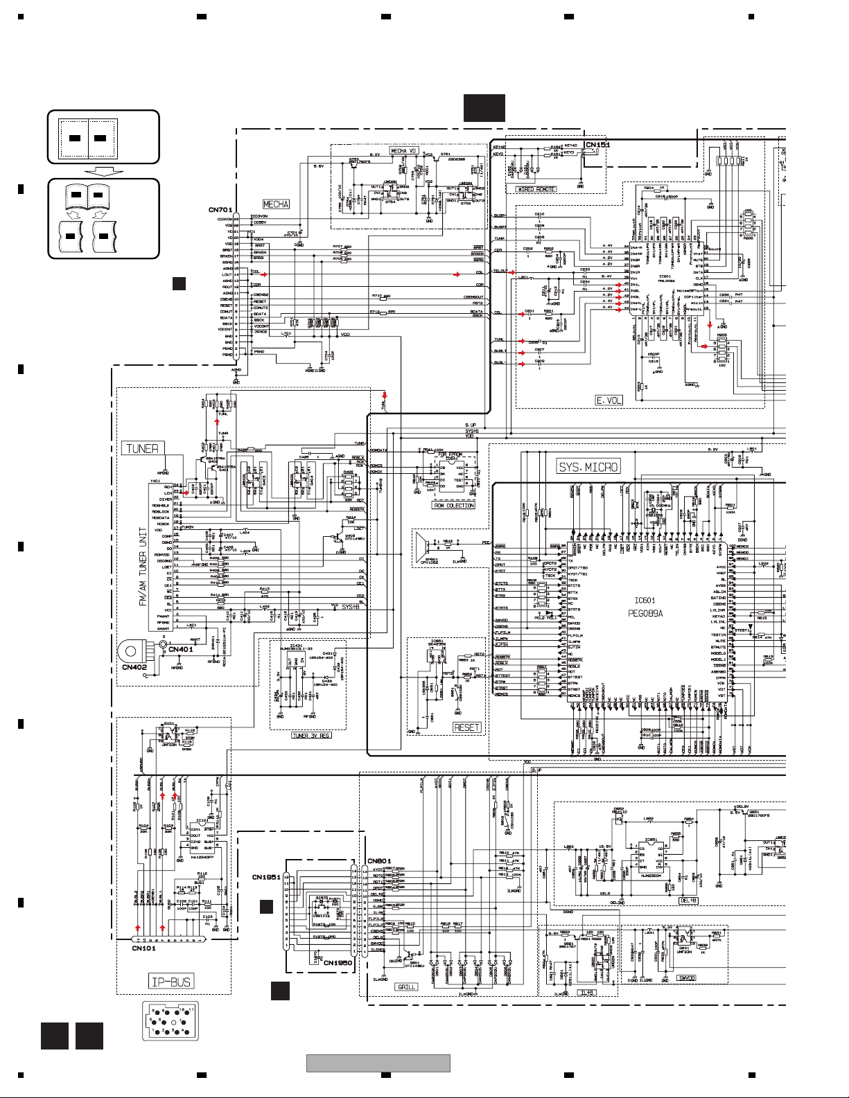
1234
8
A
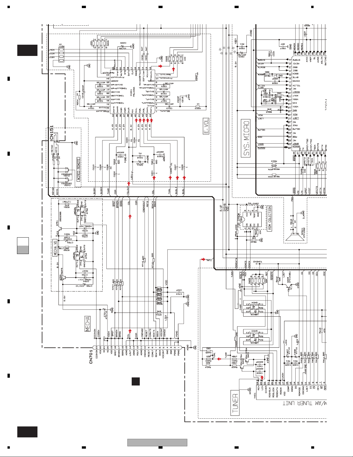
4. PCB CONNECTION DIAGRAM
4.1 TUNER AMP UNIT
A
B
C
NOTE FOR PCB DIAGRAMS
1.The parts mounted on this PCB
include all necessary parts for
several destination.
For further information for
respective destinations, be sure
to check with the schematic dia gram.
2.Viewpoint of PCB diagrams
Connector
Capacitor
SIDE A
P.C.Board
Chip Part
SIDE B
CORD ASSY(REAR OUTPUT)
CORD ASSY(MICROPHONE INPUT)
TUNER AMP UNIT
A
150
140
130
120
110
100
90
WIRED REMOTE
CONTROL
1
2
3
IP-BUS
4
CORD
123
5637
891011
80
70
D
60
50
40
E
30
20
10
DSENSE
RESET
Y
F
40
0
A
DEH-P70BT/EW
1234
10 20 30 40 50 60 70
X
CN1051
E
FRONT
Page 41

5678
CORD ASSY(POWER SUPPLY, SPEAKER)
FRONT
OUTOUT
SUB WOOFER OUTOUT OR
NON FADING OUTPUT
LR LR
3
42
1
7
86
SIDE A
A
3
5
B
2
FM/AM ANTENNA
1
C
FM/AM TUNER UNIT
1 2 3 4 5 6 7 8 9 101112 1314 15161718192021222324
RESET
70 80 90 100 110 120 130 140 150 160 170
FRONT
CN901
C
56
D
CN1950
DEH-P70BT/EW
7
D
E
F
A
8
41
Page 42

1234
A
TUNER AMP UNIT
A
1
B
1
C
STEST1
PCL1
D
E
1
F
90100110120130140150160170
A
42
1234
DEH-P70BT/EW
Page 43

5678
SIDE B
A
150
1
140
130
B
120
110
100
C
90
80
70
60
50
40
30
20
10
D
E
102030405060708090 0
DEH-P70BT/EW
56
Y
F
X
A
7
8
43
Page 44

1234
4.2 KEYBOARD UNIT
KEYBOARD UNIT
B
A
B
C
EQ
DISP
TA
160
150
140
130
120
110
100
SIDE A
90
80
123456
70
D
4
10
6
7
5
2
E
MULTI-CONTROL
8
9
3
1
BAND
60
50
40
30
20
SRC
ATT
LIST
F
B
44
1234
PHONE
DEH-P70BT/EW
10203040
X
10
Y
0
Page 45

5678
KEYBOARD UNIT
B
160
150
140
130
120
110
100
TP7
TP6
TP5
D
SIDE B
A
CN1951
B
C
90
80
70
60
50
40
30
D
E
20
10
Y
0
56
10 20 30 40
X
DEH-P70BT/EW
F
B
7
8
45
Page 46

1234
4.3 CD CORE UNIT(S10.1)
CD CORE UNIT(S10.1)
C
A
M2
LOADING
B
/CARRIAGE
MOTOR
M1
SPINDLE
MOTOR
SIDE A
C
D
PICKUP UNIT(P10)(SERVICE)
E
A
CN701
HOME
EF
REFO1
F
C
46
1234
DEH-P70BT/EW
Page 47

5678
CD CORE UNIT(S10.1)
C
SIDE B
A
DSCSNS
8EJ
12EJ
B
C
C
D
E
F
56
DEH-P70BT/EW
7
8
47
Page 48

1234
4.4 PANEL UNIT
A
PANEL UNIT
D
CN1501
B
B
C
SIDE A
EJECT
PANEL UNIT
D
E
F
D
A
CN801
SIDE B
48
D
DEH-P70BT/EW
1234
Page 49

5678
4.5 ANTENNA PCB
A
ANTENNA PCB
F
E
20
10
Y
X
ANT1001
SIDE A
ANTENNA PCB
F
BT ANTENNA
SIDE B
20
10
B
Y
C
10 20 300
102030 0
X
F
D
E
F
56
DEH-P70BT/EW
7
8
49
Page 50

1234
4.6 BLUETOOTH PCB
BLUETOOTH PCB
A
E
SIDE A
A
B
C
40
30
20
D
10
E
Y
0
F
X
10 20 30
50
E
DEH-P70BT/EW
1234
Page 51

5678
BLUETOOTH PCB
E
SIDE B
40
30
A
B
C
20
D
10
E
Y
102030
X
0
F
ANT1102
F
56
DEH-P70BT/EW
E
7
8
51
Page 52

1234
5. ELECTRICAL PARTS LIST
NOTE:
A
• Parts whose parts numbers are omitted are subject to being not supplied.
• The part numbers shown below indicate chip components.
Chip Resistor
RS1/_S___J,RS1/__S___J
Chip Capacitor (except for CQS.....)
CKS....., CCS....., CSZS.....
• The > mark found on some component parts indicatesthe importance of the safety factor of the part.
Therefore, when replacing, be sure to use parts of identical designation.
• Meaning of the figures and others in the parentheses in the parts list.
B
Example) IC 301 is on the point (face A, 91 of x-axis, and 111 of y-axis) of the corresponding
PC board.
IC 301 (A, 91, 111) IC NJM2068V
Circuit Symbol and No. Part No.
Unit Number : CWM9941
Unit Name : Tuner Amp Unit
Unit Number : CWM9942
Unit Name : Bluetooth Unit
C
Unit Number : CWM9943
Unit Name : Keyboard Unit
Unit Number : CWM8758
Unit Name : Panel Unit
Unit Number : CWX3096
Unit Name : CD Core Unit(S10.1)
D
A
Unit Number : CWM9941
Unit Name : Tuner Amp Unit
MISCELLANEOUS
IC 101 (B,35,116) IC HA12240FP
IC 201 (A,88,94) IC PML009A
IC 241 (A,109,78) IC NJM4558MD
IC 351 (A,104,139) IC PAL007B
E
IC 431 (B,146,26) IC NJM2391DL1-33
IC 451 (B,64,55) IC NJM2391DL1-33
IC 501 (A,97,73) IC TC74VHCT08AFTS1
IC 521 (A,98,66) IC TC74VHC08FTS1
IC 541 (A,98,59) IC S99-50084
IC 581 (A,53,76) IC AN6123MS
IC 601 (A,137,77) IC PEG089A
IC 651 (B,121,45) IC BD4835G
IC 851 (A,44,26) IC NJM2360M
IC 911 (A,5,120) IC NJM2388F84
Q 101 (A,29,123) Transistor UMF23N
F
Q 301 (A,142,129) Transistor IMH23
Q 302 (A,63,84) Transistor IMH23
Q 303 (A,158,128) Transistor IMH23
Circuit Symbol and No. Part No.
Q 304 (A,156,121) Transistor UMD2N
Q 351 (B,120,137) Transistor DTC114EU
Q 352 (B,121,132) Transistor DTC124EU
Q 381 (A,136,129) Transistor 2SC4081
Q 401 (B,156,44) Transistor 2SA1576A
Q 402 (B,156,40) Transistor 2SA1576A
Q 403 (A,150,52) Transistor UMH1N
Q 404 (A,150,55) Transistor UMH1N
Q 405 (B,158,76) Transistor DTC143EU
Q 551 (A,6,103) Transistor 2SD2396
Q 552 (A,15,90) Transistor 2SB1243
Q 553 (B,26,82) Transistor DTC114EU
Q 591 (A,80,78) Transistor DTC314TU
Q 751 (A,6,70) Transistor 2SD2396
Q 752 (A,22,74) Transistor UMD2N
Q 753 (A,21,49) Transistor 2SD1760F5
Q 754 (A,21,58) Transistor UMD2N
Q 801 (B,103,25) Transistor DTC143EU
Q 821 (A,18,27) Transistor 2SD1767
Q 822 (A,25,16) Transistor UMD2N
Q 831 (A,73,21) Transistor UMF23N
Q 851 (A,21,34) Transistor 2SD1760F5
Q 852 (A,29,41) Transistor UMD2N
Q 901 (B,37,61) Transistor 2SD1760F5
Q 902 (A,33,71) Transistor UMD2N
Q 921 (A,75,116) Transistor UMX1N
Q 941 (B,85,112) Transistor DTC114EU
Q 951 (B,86,118) Transistor 2SA1576A
D 151 (A,11,129) Diode DAN202U
D 152 (B,6,134) Diode DAP202U
D 241 (A,91,79) Diode Network DA204U
D 242 (A,114,86) Diode Network DA204U
D 243 (B,112,83) Diode DAN202U
D 244 (B,112,87) Diode DAP202U
D 251 (B,118,82) Diode RB706F-40
D 301 (A,123,125) Diode 1SS133
D 381 (A,123,128) Diode HZS9L(A2)
D 382 (A,131,129) Diode DAN202U
D 431 (A,138,25) Diode 1SR154-400
D 432 (A,141,25) Diode 1SR154-400
D 433 (A,145,25) Diode 1SR154-400
52
1234
DEH-P70BT/EW
Page 53

5678
Circuit Symbol and No. Part No.
D 551 (B,22,89) Diode UDZS5R6(B)
D 591 (A,73,76) Diode 1SS355
D 651 (B,112,48) Diode 1SS355
D 751 (A,16,71) Diode HZS9L(A2)
D 754 (A,15,57) Diode HZS6L(C1)
D 801 (B,122,29) Diode DAP202U
D 802 (B,120,23) Diode DAN202U
D 803 (B,129,23) Diode DAP202U
D 804 (B,129,19) Diode DAN202U
D 805 (B,111,30) Diode DAP202U
D 806 (B,111,24) Diode DAN202U
D 821 (A,24,26) Diode HZS11L(A1)
D 851 (A,33,36) Diode HZS11L(A1)
D 852 (B,37,20) Diode RB411D
D 901 (A,37,81) Diode MPG06G-6415G50
D 902 (A,37,67) Diode HZS6L(B1)
D 921 (A,67,115) Diode HZS7L(C3)
D 922 (A,71,115) Diode HZS7L(A1)
D 931 (A,81,114) Diode HZS9L(B3)
D 932 (A,87,114) Diode Network DA204U
D 941 (A,66,108) Diode MPG06G-6415G50
D 951 (B,69,126) Diode DAN202U
D 961 (A,111,118) Diode MPG06G-6415G50
D 962 (A,108,118) Diode MPG06G-6415G50
D 981 (A,46,125) Diode MPG06G-6415G50
D 982 (A,54,117) Diode MPG06G-6415G50
ZNR401 (A,160,109)Surge Protector RCCA-201Q31UA-PI
L 101 (B,49,113) Inductor LCTC1R0K1608
L 201 (A,71,102) Inductor LCTAW2R2J2520
L 401 (B,157,103) Inductor LCTAW4R7J2520
L 402 (A,152,95) Inductor LAU1R0K
L 403 (A,154,74) Inductor LAU1R0K
L 404 (A,154,53) Inductor LAU2R2K
L 501 (A,92,71) Inductor CTF1379
L 521 (A,92,70) Inductor CTF1379
L 541 (A,92,58) Inductor CTF1379
L 581 (A,58,75) Inductor CTF1379
L 601 (A,119,68) Ferri-Inductor LAU100K
L 602 (A,132,91) Inductor LCTC1R0K1608
L 701 (A,112,51) Ferri-Inductor LAU100K
L 831 (A,84,21) Ferri-Inductor LAU100K
L 852 (A,31,25) Inductor CTF1618
L 853 (A,45,19) Inductor LCTAW2R2J3225
L 951 (B,61,127) Inductor LCTAW2R2J3225
L 981
X 601 (A,124,77)Crystal Resonator 15.000MHz CSS1653
S 651 (A,73,10) Switch(RESET) CSG1020
S 802 (A,25,10) Switch(DSENSE) CSN1039
VR251 (A,105,109)Semi-fixed 10kΩ(B) CCP1229
(A,34,106)Choke Coil 600µH CTH1280
>FU301 (A,157,124) Fuse 3A CEK1286
>FU302 (A,53,88) Fuse 3A CEK1286
MIC251 (A,97,121) Microphone CPM1068
SP601 (A,58,13) Buzzer CPV1062
> Fuse 10A CEK1208
FM/AM Tuner Unit CWE1801
RESISTORS
R 101 (B,27,121) RS1/16S102J
R 102 (B,29,124) RS1/16S102J
56
R 103 (B,26,124) RS1/16S223J
R 104 (B,33,120) RS1/16S223J
R 105 (B,26,129) RS1/16S181J
R 106 (B,31,124) RS1/16S181J
R 107 (B,33,124) RS1/16S222J
R 108 (B,53,108) RS1/16S101J
R 109 (B,127,107) RS1/16S101J
R 110 (B,48,111) RS1/16S102J
R 111 (B,41,129) RS1/16S101J
R 112 (B,39,129) RS1/16S101J
R 113 (B,41,133) RS1/16S470J
R 114 (B,39,134) RS1/16S150J
R 115 (A,26,124) RS1/16S332J
R 116 (A,26,122) RS1/16S562J
R 151 (B,6,138) RS1/16S102J
R 152 (B,4,139) RS1/16S102J
R 201 (B,81,93) RS1/16S821J
R 202 (B,81,97) RS1/16S821J
R 203 (B,80,86) RS1/16S102J
R 204 (B,80,102) RS1/16S102J
R 205 (A,98,88) RAB4C101J
R 206 (A,99,100) RAB4C101J
R 211 (A,99,95) RAB4C102J
R 241 (A,103,78) RS1/16S104J
R 242 (A,114,76) RS1/16S104J
R 243 (A,101,78) RS1/16S563J
R 244 (A,116,77) RS1/16S563J
R 245 (A,95,79) RS1/16S474J
R 246 (A,113,82) RS1/16S474J
R 251 (B,121,96) RS1/16S104J
R 252 (B,119,85) RS1/16S104J
R 253 (A,97,110) RS1/16S222J
R 254 (A,97,109) RS1/16S561J
R 301 (B,139,128) RS1/16S821J
R 302 (B,141,128) RS1/16S821J
R 305 (B,135,139) RS1/16S223J
R 306 (B,140,139) RS1/16S223J
R 307 (B,70,88) RS1/16S821J
R 308 (B,58,84) RS1/16S821J
R 311 (B,65,87) RS1/16S223J
R 312 (B,61,87) RS1/16S223J
R 313 (B,157,128) RS1/16S821J
R 314 (B,159,128) RS1/16S821J
R 317 (B,149,139) RS1/16S223J
R 318 (B,154,139) RS1/16S223J
R 319 (A,148,121) RS1/16S102J
R 351 (B,80,136) RS1/16S153J
R 352 (B,125,130) RS1/16S103J
R 353 (B,114,143) RS1/16S103J
R 354 (B,120,141) RS1/16S331J
R 355 (B,116,141) RS1/16S101J
R 357 (A,121,120) RS1/16S331J
R 358 (B,112,126) RS1/16S331J
R 359 (A,119,120) RS1/16S331J
R 360 (B,114,126) RS1/16S331J
R 381 (A,120,134) RS1/16S104J
R 382 (A,121,134) RS1/16S473J
R 383 (A,130,126) RS1/16S472J
R 384 (A,133,127) RS1/16S473J
R 401 (B,156,48) RS1/16S182J
DEH-P70BT/EW
Circuit Symbol and No. Part No.
7
8
A
B
C
D
E
F
53
Page 54

1234
Circuit Symbol and No. Part No.
R 402 (B,156,38) RS1/16S182J
R 403 (A,155,44) RS1/16S821J
R 404 (A,155,42) RS1/16S821J
A
R 405 (A,144,55) RAB4C223J
R 406 (B,159,64) RS1/16S681J
R 407 (B,159,79) RS1/16S681J
R 408 (B,159,81) RS1/16S681J
R 409 (B,159,84) RS1/16S681J
Circuit Symbol and No. Part No.
R 642 (A,118,58) RS1/16S103J
R 643 (A,121,58) RS1/16S103J
R 651 (B,117,46) RS1/16S183J
R 652 (B,113,44) RS1/16S102J
R 653 (B,112,46) RS1/16S102J
R 701 (B,80,26) RS1/16S473J
R 703 (B,85,39) RS1/16S682J
R 704 (B,85,37) RS1/16S682J
R 410 (B,159,86) RS1/16S681J
R 411 (B,159,90) RS1/16S681J
R 412 (B,159,92) RS1/16S681J
R 413 (A,143,51) RS1/16S471J
R 414 (B,158,72) RS1/16S103J
B
R 425 (B,150,49) RS1/16S0R0J
R 426 (B,153,42) RS1/16S0R0J
R 501 (B,86,73) RS1/16S681J
R 502 (B,93,74) RS1/16S681J
R 503 (B,100,66) RS1/16S681J
R 504 (B,100,68) RS1/16S681J
R 505 (B,100,70) RS1/16S681J
R 506 (B,100,72) RS1/16S681J
R 521 (A,104,66) RAB4C681J
R 522 (A,92,65) RAB4C681J
R 523 (B,135,58) RS1/16S122J
C
R 524 (B,133,55) RS1/16S332J
R 525 (B,135,55) RS1/16S332J
R 526 (B,138,60) RS1/16S182J
R 541 (A,104,59) RAB4C101J
R 542 (A,92,61) RS1/16S101J
R 543 (A,92,62) RS1/16S101J
R 551 (B,8,104) RS1/16S472J
R 552 (B,21,84) RS1/16S223J
R 553 (A,15,86) RD1/4PU152J
R 705 (B,85,29) RS1/16S682J
R 706 (B,85,27) RS1/16S682J
R 707 (B,102,42) RS1/16S221J
R 708 (B,102,40) RS1/16S221J
R 709 (B,102,37) RS1/16S221J
R 710 (B,105,36) RS1/16S221J
R 712 (B,105,31) RS1/16S221J
R 751 (A,16,75) RD1/4PU271J
R 752 (A,15,60) RD1/4PU391J
R 801 (B,108,24) RS1/16S222J
R 802 (A,44,9) RS1/16S101J
R 803 (B,115,24) RS1/16S222J
R 804 (B,119,10) RS1/16S222J
R 805 (B,117,24) RS1/16S222J
R 806 (B,126,21) RS1/16S222J
R 807 (B,124,22) RS1/16S222J
R 808 (B,117,32) RS1/16S102J
R 809 (A,26,18) RS1/16S102J
R 810 (B,116,28) RS1/16S473J
R 811 (B,118,28) RS1/16S473J
R 812 (B,110,27) RS1/16S473J
R 813 (B,128,26) RS1/16S104J
R 815 (A,15,23) RS1/16S101J
R 816 (A,14,26) RS1/16S101J
R 817 (A,12,26) RS1/16S101J
R 554 (A,115,61) RS1/16S0R0J
R 556 (A,15,94) RD1/4PU0R0J
D
R 581 (A,51,79) RS1/16S105J
R 582 (A,72,84) RS1/16S332J
R 584 (A,62,76) RS1/16S0R0J
R 596 (A,77,78) RS1/16S223J
R 597 (A,83,78) RS1/16S102J
R 601 (A,129,91) RS1/16S104J
R 602 (B,129,81) RS1/16S0R0J
R 603 (A,134,98) RS1/16S473J
R 604 (A,135,100) RS1/16S472J
R 605 (A,133,100) RS1/16S472J
R 606 (A,135,64) RAB4C681J
E
R 607 (A,142,65) RAB4C681J
R 608 (A,149,71) RS1/16S681J
R 609 (A,149,72) RS1/16S681J
R 610 (A,149,74) RS1/16S681J
R 611 (A,131,100) RS1/16S104J
R 612 (A,129,100) RS1/16S104J
R 613 (A,128,99) RS1/16S104J
R 614 (A,138,89) RS1/16S473J
R 615 (A,135,91) RS1/16S103J
R 616 (A,72,17) RS1/16S102J
R 618 (B,133,85) RS1/16S104J
F
R 619 (A,125,68) RS1/16S681J
R 821 (A,18,24) RS1/16S121J
R 822 (A,24,21) RS1/16S121J
R 823 (B,20,31) RS1/16S1R0J
R 824 (B,19,28) RS1/16S473J
R 825 (A,24,18) RS1/16S121J
R 831 (B,70,26) RS1/16S472J
R 832 (B,65,26) RS1/16S102J
R 833 (B,76,25) RS1/16S472J
R 851 (B,29,43) RS1/16S331J
R 852 (B,25,43) RS1/16S331J
R 854 (B,48,28) RS1/16S1R0J
R 855 (B,43,28) RS1/16S391J
R 856 (B,47,30) RS1/16S121J
R 857 (A,42,35) RD1/4PU302J
R 858 (A,42,33) RD1/4PU302J
R 901 (A,33,75) RS1/16S821J
R 902 (A,34,77) RS1/16S333J
R 903 (A,33,73) RS1/16S821J
R 911 (B,8,113) RS1/16S473J
R 921 (B,67,121) RS1/16S472J
R 922 (B,62,122) RS1/16S473J
R 923 (B,77,119) RS1/16S103J
R 924 (B,65,121) RS1/16S473J
R 925 (B,74,120) RS1/16S104J
R 931 (A,85,116) RS1/16S392J
R 620 (B,131,83) RS1/16S104J
R 641 (A,115,58) RS1/16S104J
54
1234
R 932 (A,85,114) RS1/16S223J
R 933 (A,88,116) RS1/16S102J
DEH-P70BT/EW
Page 55

5678
Circuit Symbol and No. Part No.
R 941 (B,72,109) RS1/16S103J
R 951 (B,82,121) RS1/16S472J
R 952 (B,86,115) RS1/16S102J
R 953 (B,80,121) RS1/16S472J
R 954 (B,78,119) RS1/16S104J
R 955 (B,66,127) RS1/16S153J
R 971 (A,45,68) RS1/16S220J
R 972 (A,63,81) RS1/16S102J
R 981 (A,61,115) RD1/4PU102J
R 982 (A,76,111) RS1/16S392J
R 983 (A,64,115) RD1/4PU102J
CAPACITORS
C 101 (B,34,137) CCSRCH101J50
C 102 (B,36,137) CCSRCH101J50
C 103 (B,32,137) CKSRYB104K50
C 104 (B,38,122) CKSRYB102K50
C 105 (B,38,124) CKSRYB102K50
C 106 (B,37,120) CKSRYB104K50
C 201 (B,81,91) CKSRYB105K10
C 202 (B,81,95) CKSRYB105K10
C 203 (B,86,90) CCSQCH222J50
C 204 (B,87,97) CCSQCH222J50
C 205 (A,79,93) CKSRYB104K50
C 206 (A,79,96) CKSRYB104K50
C 207 (A,79,91) CKSRYB105K10
C 208 (A,79,98) CKSRYB105K10
C 209 (A,79,90) CKSRYB105K10
C 210 (A,79,99) CKSRYB105K10
C 211 (A,73,95) CEAL470M10
C 212 (B,71,95) CKSRYB104K50
C 213 (A,80,83) CEALNP4R7M35
C 214 (A,80,105) CEALNP4R7M35
C 215 (A,79,88) CCSQCH152J50
C 216 (A,74,106) CCSQCH152J50
C 217 (A,87,83) CEALNP4R7M35
C 218 (A,87,105) CEALNP4R7M35
C 219 (A,93,83) CEALNP4R7M35
C 220 (A,93,105) CEALNP4R7M35
C 221 (A,100,83) CEALNP4R7M35
C 222 (A,100,105) CEALNP4R7M35
C 229 (A,105,97) CEAL100M25
C 230 (A,100,92) CKSRYB474K10
C 231 (A,100,91) CKSRYB474K10
C 233 (B,87,95) CKSRYB104K50
C 234 (B,87,93) CKSRYB104K50
C 241 (A,101,77) CKSRYB104K50
C 242 (A,116,76) CKSRYB104K50
C 243 (A,99,79) CKSRYB104K50
C 244 (A,114,79) CKSRYB104K50
C 245 (A,97,79) CKSRYB474K10
C 246 (A,113,84) CKSRYB474K10
C 247 (A,94,79) CCSRCH101J50
C 248 (A,114,81) CCSRCH101J50
C 249 (A,110,82) CKSRYB104K50
C 251 (A,105,91) CEALNP100M16
C 252 (A,101,114) CEAL220M16
C 253 (A,93,114) CEAL100M25
C 301 (A,136,123) CEAL100M25
56
C 302 (A,136,110) CEAL100M25
C 303 (A,68,83) CEVW100M16
C 304 (A,58,84) CEVW100M16
C 305 (A,143,123) CEAL100M25
C 306 (A,140,116) CEAL100M25
C 310 (A,129,114) CEAL220M35
C 351 (A,123,120) CKSRYB474K10
C 352 (B,110,126) CKSRYB474K10
C 353 (A,117,120) CKSRYB474K10
C 354 (B,116,126) CKSRYB474K10
C 355 (A,125,120) CKSQYB225K10
C 356 (A,123,117) CKSQYB225K10
C 357 (A,129,122) CEAL100M25
C 358 (B,50,123) CKSRYB104K50
C 359 (A,48,125) 3300µF/16V CCH1486
C 360 (B,111,141) CKSQYB105K16
C 361 (A,126,133) CEHAS330M10
C 363 (A,121,117) CKSQYB474K16
C 364 (B,115,120) CKSQYB474K16
C 365 (A,119,117) CKSQYB474K16
C 366 (B,117,120) CKSQYB474K16
C 367 (B,131,127) CKSRYB103K50
C 368 (A,128,107) CKSRYB104K50
C 401 (B,160,44) CKSRYB222K50
C 402 (B,160,41) CKSRYB222K50
C 405 (B,164,59) CKSRYB103K50
C 406 (B,164,64) CKSRYB103K50
C 407 (A,153,60) CEJQ470M10
C 408 (A,153,66) CEJQ470M10
C 410 (B,164,96) CKSRYB103K50
C 411 (A,151,102) CEAL101M10
C 412 (A,155,47) CKSRYB103K50
C 413 (A,146,47) CEJQ101M10
C 416 (A,154,97) CKSRYB104K50
C 425 (A,142,38) CKSRYB105K10
C 426 (B,62,96) CKSRYB105K10
C 431 (A,155,26) CKSYB475K10
C 432 (B,153,28) CKSRYB103K50
C 433 (B,153,24) CKSRYB103K50
C 434 (A,154,32) CEJQ220M25
C 451 (B,57,50) CKSRYB103K50
C 452 (B,60,60) CKSRYB103K50
C 453 (A,46,59) CEAL220M16
C 454 (B,57,48) CKSYB475K10
C 501 (A,92,74) CKSRYB104K50
C 521 (A,92,68) CKSRYB104K50
C 541 (A,92,59) CKSRYB104K50
C 551 (A,26,78) CEHAS101M10
C 552 (B,20,89) CKSRYB103K50
C 553 (A,16,81) CEHAS101M10
C 554 (A,25,88) 470µF/16V CCH1339
C 581 (A,47,71) CKSYB106K6R3
C 582 (A,48,77) CKSYB106K6R3
C 583 (A,65,79) CCSRCH331J50
C 584 (A,71,79) CKSRYB334K10
C 602 (B,121,66) CKSRYB103K50
C 603 (A,120,63) CEAL4R7M50
C 604 (B,126,79) CCSRCH200J50
C 605 (B,126,76) CCSRCH180J50
C 606 (A,149,75) CCSRCH470J50
DEH-P70BT/EW
Circuit Symbol and No. Part No.
7
8
A
B
C
D
E
F
55
Page 56

1234
Circuit Symbol and No. Part No.
C 607 (B,144,83) CKSYB475K10
C 608 (A,124,70) CKSRYB221K50
C 609 (B,142,85) CCSRCH101J50
A
C 610 (B,139,81) CCSRCH101J50
Circuit Symbol and No. Part No.
L 1001 (B,8,30) Inductor LCTAW1R0J2520
L 1041 (B,8,33) Inductor LCYC2R2K1608
Y 1001 (B,18,21) BT Module CWX3131
ANT1101 (B,9,8) BT Antenna CWX3132
C 611 (B,131,118) CCSRCH101J50
C 641 (A,114,54) CKSRYB104K50
C 651 (B,112,53) CKSRYB105K10
C 701 (A,92,53) 470µF/10V CCH1438
C 704 (B,85,25) CCSRCH101J50
C 751 (B,16,69) CKSRYB473K50
C 752 (B,10,69) CKSRYB102K50
C 753 (A,15,66) CEHAS101M10
C 754 (B,9,58) CKSRYB473K50
C 755 (A,27,57) CEHAS101M10
B
C 821 (A,21,24) CKSRYB473K50
C 831 (B,78,25) CCSRCH101J50
C 832 (B,83,18) CKSRYB105K10
C 833 (B,76,20) CKSRYB473K50
C 851 (B,34,32) CKSRYB104K50
C 852 (A,35,46) CEHAS470M16
C 853 (A,41,41) CEHAS101M10
C 854 (B,48,23) CKSRYB104K50
C 855 (B,43,23) CCSRCH331J50
C 856 (B,43,30) CKSRYB103K50
C
C 857 (A,34,13) CEJQ330M25
C 858 (A,40,13) CEJQ100M50
C 859 (A,41,19) 4.7µF CCG1111
C 861 (A,82,11) 4.7µF CCG1111
C 901 (A,37,55) 470µF/16V CCH1339
C 902 (A,26,67) 470µF/16V CCH1339
C 903 (A,37,65) CKSRYB472K50
C 904 (B,39,70) CKSRYB103K50
C 905 (A,39,73) CEHAS101M10
C 911 (A,15,107) 100µF/25V CCH1316
C 912 (B,8,117) CKSRYB103K50
D
C 913 (A,15,99) CEHAS101M10
C 921 (B,70,121) CKSRYB104K50
C 931 (A,83,114) CKSRYB104K50
C 941 (B,77,112) CKSQYB105K16
C 951 (B,61,124) CKSRYB104K50
C 961 (B,106,118) CKSRYB473K50
C 971 (A,46,82) CEVW330M10
C 981 (B,60,140) CKSRYB473K50
Bluetooth Unit
Consists of
E
Bluetooth PCB
Antenna PCB
EF
Unit Number : CWM9942
Unit Name : Bluetooth Unit
RESISTORS
R 1001 (A,21,17) RS1/16S681J
R 1002 (A,8,12) RS1/16S0R0J
R 1003 (A,21,15) RS1/16S681J
R 1004 (A,10,15) RS1/16S103J
R 1005 (A,8,18) RS1/16S0R0J
R 1006 (A,29,22) RS1/16S103J
R 1007 (B,9,26) RS1/16S0R0J
R 1008 (A,9,22) RS1/16S103J
R 1009 (A,29,23) RS1/16S473J
R 1010 (A,29,27) RS1/16S334J
R 1021 (B,25,43) RS1/16S203J
R 1022 (B,25,40) RS1/16S203J
R 1023 (B,30,42) RS1/16S103J
R 1024 (B,30,40) RS1/16S103J
R 1031 (B,12,39) RS1/16S393J
R 1032 (B,12,42) RS1/16S393J
R 1033 (B,9,41) RS1/16S103J
R 1034 (B,9,42) RS1/16S103J
R 1041 (A,23,29) RAB4C101J
R 1042 (A,29,30) RS1/16S104J
R 1043 (A,28,30) RS1/16S473J
R 1051 (B,6,40) RS1/16S0R0J
R 1052 (A,10,35) RS1/16S0R0J
R 1053 (A,12,35) RS1/16S681J
R 1054 (A,13,35) RS1/16S0R0J
R 1055 (A,15,35) RS1/16S681J
R 1056 (A,24,34) RS1/16S681J
R 1057 (A,24,36) RS1/16S681J
R 1058 (B,30,44) RS1/16S0R0J
R 1059 (A,30,36) RS1/16S681J
CAPACITORS
C 1001 (B,7,11) CCSRCH101J50
C 1002 (B,7,9) CSZS1R0M16
C 1003 (B,7,12) CKSRYB104K50
C 1004 (B,7,15) CKSRYB104K50
C 1005 (B,7,16) CSZS4R7M16
C 1006 (B,7,20) CKSRYB104K50
C 1007 (B,7,19) CSZS100M16
C 1010 (B,27,31) CKSRYB104K50
C 1021 (B,27,43) CCSRCH101J50
C 1022 (B,27,40) CCSRCH101J50
C 1023 (B,30,43) CKSRYB105K10
C 1024 (B,30,39) CKSRYB105K10
C 1026 (B,30,37) CKSRYB105K10
C 1031 (B,12,41) CCSRCH101J50
C 1032 (B,12,44) CKSRYB105K10
MISCELLANEOUS
IC 1041 (B,19,40) IC AK2301A
Q 1001 (B,29,18) Transistor DTC124EU
F
Q 1002 (B,29,22) Transistor DTC124EU
Q 1041 (B,30,26) Transistor DTC124EU
Q 1042 (B,30,30) Transistor DTC124EU
56
1234
C 1033 (B,9,39) CKSRYB105K10
C 1034 (B,9,44) CKSRYB105K10
C 1041 (B,8,34) CKSRYB104K50
C 1042 (B,8,36) CSZS100M16
C 1043 (B,30,36) CKSRYB105K10
C 1044 (B,30,35) CKSRYB334K10
DEH-P70BT/EW
Page 57

5678
Circuit Symbol and No. Part No.
B
Unit Number :
Unit Name : Keyboard Unit
MISCELLANEOUS
IC 1551 (A,127,23) IC S-818A33AUC-BGN
IC 1561 (B,80,18) IC PEG088A
IC 1562 (A,151,24) IC TSOP4840SB1
IC 1563 (A,110,22) IC PD8140A
Q 1501 (A,29,38) Transistor DTC114EU
Q 1591 (B,69,34) Transistor 2SC4617
Q 1592 (B,70,31) Transistor 2SD1664
D 1503 (A,24,24) LED SML412BC5T(MN)
D 1504 (A,41,40) LED SML412BC5T(MN)
D 1505 (A,41,7) LED SML412BC5T(MN)
D 1506 (A,58,24) LED SML412BC5T(MN)
D 1507 (A,16,40) LED SML412BC5T(MN)
D 1508 (A,152,40) LED SML412BC5T(MN)
D 1531 (A,17,34) LED SML412BC5T(MN)
D 1532 (A,17,14) LED SML412BC5T(MN)
D 1533 (A,59,5) LED SML412BC5T(MN)
D 1534 (A,15,23) LED SML412BC5T(MN)
D 1535 (A,23,5) LED SML412BC5T(MN)
D 1536 (A,76,5) LED SML412BC5T(MN)
D 1537 (A,87,5) LED SML412BC5T(MN)
D 1538 (A,134,5) LED SML412BC5T(MN)
D 1539 (A,99,5) LED SML412BC5T(MN)
D 1540 (A,152,16) LED SML412BC5T(MN)
D 1541 (A,122,5) LED SML412BC5T(MN)
D 1542 (A,110,5) LED SML412BC5T(MN)
D 1543 (A,145,5) LED SML412BC5T(MN)
D 1544 (A,152,32) LED SML412BC5T(MN)
D 1561 (B,63,22) Diode 1SS355
L 1501 (A,129,30) Inductor CTF1617
L 1551 (A,122,17) Inductor CTF1617
TH1591 (B,73,35) Thermistor CCX1037
X 1561
S 1501 (A,41,24) Switch(MULTI-CONTROL) CSX1065
S 1531 (A,18,31) Push Switch CSG1155
S 1532 (A,18,17) Push Switch CSG1155
S 1533 (A,66,5) Push Switch CSG1155
S 1534 (A,16,26) Push Switch CSG1155
S 1535 (A,17,5) Push Switch CSG1155
S 1536 (A,77,7) Push Switch CSG1155
S 1537 (A,89,7) Push Switch CSG1155
S 1538 (A,135,7) Push Switch CSG1155
S 1539 (A,101,7) Push Switch CSG1155
S 1540 (A,152,13) Push Switch CSG1155
S 1541 (A,124,7) Push Switch CSG1155
S 1542 (A,112,7) Push Switch CSG1155
S 1543 (A,145,7) Push Switch CSG1155
S 1544 (A,152,34) Push Switch CSG1155
VR1591
VR1592 (B,115,13)Semi-fixed 15kΩ(B) CCP1230
RESISTORS
(B,69,19)Ceramic Resonator 16.000MHz CSS1616
(B,120,13) Semi-fixed 15kΩ(B) CCP1230
OEL Unit MXS8221
Circuit Symbol and No. Part No.
R 1503 (A,134,29) RS1/16S222J
R 1505 (B,145,33) RS1/16S102J
R 1506 (B,147,35) RS1/16S102J
R 1508 (A,128,33) RS1/16S103J
R 1509 (A,75,17) RS1/16S103J
R 1510 (B,44,20) RS1/16S222J
R 1511 (B,46,23) RS1/16S332J
R 1512 (B,44,23) RS1/16S822J
R 1513 (B,43,21) RS1/16S4702D
R 1514 (B,45,40) RS1/16S561J
R 1516 (B,55,24) RS1/16S561J
R 1518 (A,23,37) RS1/16S271J
R 1520 (B,153,32) RS1/16S821J
R 1531 (B,18,21) RS1/16S331J
R 1533 (B,22,7) RS1/16S561J
R 1535 (B,19,12) RS1/16S561J
R 1537 (B,123,6) RS1/16S331J
R 1539 (B,148,7) RS1/16S331J
R 1541 (A,102,5) RS1/16S331J
R 1543 (B,150,11) RS1/16S561J
R 1551 (A,124,21) RS1/16S222J
R 1561 (B,145,13) RS1/16S101J
R 1562 (B,150,18) RS1/16S103J
R 1563 (B,152,16) RS1/16S2R2J
R 1565 (B,74,8) RS1/16S104J
R 1566 (B,63,21) RS1/16S154J
R 1567 (A,77,17) RS1/16S473J
R 1568 (A,75,34) RS1/16S103J
R 1569 (A,76,26) RS1/16S473J
R 1570 (A,76,27) RS1/16S473J
R 1571 (B,55,14) RAB4C102J
R 1572 (B,55,18) RAB4C102J
R 1573 (A,73,16) RS1/16S221J
R 1574 (A,88,23) RAB4C473J
R 1575 (A,85,28) RAB4C101J
R 1576 (B,92,11) RAB4C101J
R 1577 (A,93,24) RAB4C101J
R 1578 (B,99,15) RAB4C101J
R 1579 (A,98,21) RAB4C101J
R 1580 (B,92,18) RAB4C101J
R 1581 (B,97,22) RAB4C101J
R 1582 (B,92,24) RAB4C101J
R 1583 (B,103,10) RS1/16S101J
R 1584 (B,87,30) RAB4C101J
R 1585 (B,104,11) RS1/16S101J
R 1591 (B,67,34) RS1/16S333J
R 1592 (B,72,34) RS1/16S683J
R 1593 (B,75,33) RS1/16S393J
R 1594 (B,71,27) RS1/16S392J
R 1595 (B,81,30) RAB4C101J
R 1596 (B,69,23) RS1/16S101J
R 1597 (B,70,24) RS1/16S101J
R 1598 (B,110,17) RS1/16S222J
R 1599 (B,112,16) RS1/16S222J
R 1601 (B,53,36) RS1/16S103J
R 1602 (B,61,27) RS1/16S103J
CAPACITORS
A
B
C
D
E
F
R 1501 (A,133,17) RS1/16S473J
R 1502 (A,135,29) RS1/16S222J
56
C 1505 (A,136,20) CKSRYB105K10
DEH-P70BT/EW
7
8
57
Page 58

1234
Circuit Symbol and No. Part No.
C 1510 (A,24,27) CKSRYF104Z50
C 1511 (A,46,40) CKSRYF104Z50
C 1512 (A,35,7) CKSRYF104Z50
A
C 1513 (A,59,24) CKSRYF104Z50
C 1514 (A,16,39) CKSRYF104Z50
C 1515 (A,152,37) CKSRYF104Z50
C 1531 (A,24,34) CKSRYF104Z50
C 1532 (A,24,14) CKSRYF104Z50
C 1533 (A,59,7) CKSRYF104Z50
C 1534 (A,15,20) CKSRYF104Z50
C 1535 (A,23,6) CKSRYF104Z50
C 1536 (A,72,7) CKSRYF104Z50
C 1537 (A,84,7) CKSRYF104Z50
C 1538 (A,131,7) CKSRYF104Z50
B
C 1539 (A,96,7) CKSRYF104Z50
C 1540 (A,146,16) CKSRYF104Z50
C 1541 (A,119,7) CKSRYF104Z50
C 1542 (A,107,7) CKSRYF104Z50
C 1543 (A,149,7) CKSRYF104Z50
Circuit Symbol and No. Part No.
MISCELLANEOUS
IC 201 (A,39,24) IC UPD63763GJ
IC 203 (B,45,78) IC NJM2885DL1-33
IC 301 (A,49,88) IC BA5835FP
IC 701 (A,48,51) IC PE5454B
IC 703 (A,30,44) IC S-812C33AUA-C2N
Q 101 (A,20,22) Transistor 2SA1577
Q 701 (B,62,59) Transistor UN2111
L 203 (A,53,32) Inductor CTF1389
L 207 (A,53,31) Inductor CTF1389
L 209 (A,26,20) Inductor CTF1389
L 703 (A,64,49) Inductor CTF1389
X 201 (A,51,35)Ceramic Resonator 16.934MHz CSS1603
X 701 (A,59,53)Ceramic Resonator 4.00MHz CSS1652
S 901 (A,15,43) Switch(HOME) CSN1067
S 903 (B,53,100) Switch(DSCSNS) CSN1068
S 904 (B,35,108) Switch(12EJ) CSN1067
S 905 (B,48,109) Switch(8EJ) CSN1067
C 1544 (A,146,32) CKSRYF104Z50
C 1551 (A,132,20) CSZSR4R7M16
C 1552 (A,122,22) CSZSR4R7M10
C 1553 (A,126,19) CKSRYB103K50
C 1554 (A,127,16) CSZSR4R7M10
C
C 1561 (B,63,18) CKSRYB103K50
C 1562 (A,88,20) CKSRYB103K50
C 1563 (B,70,16) CKSRYB104K50
C 1564 (B,147,16) CSZSR100M16
C 1565 (A,99,16) CKSRYB103K50
C 1566 (A,58,26) CKSRYF104Z50
C 1591 (A,87,31) CKSRYB104K50
C 1592 (A,124,32) CKSRYB104K50
C 1593 (A,122,32) CKSRYB104K50
C 1594 (A,111,31) CKSRYB104K50
C 1595 (B,67,26) CKSRYB104K50
D
C 1596 (A,118,33) CKSRYB104K50
C 1601 (B,62,32) CKSRYB103K50
D
Unit Number : CWM8758
Unit Name : Panel Unit
MISCELLANEOUS
D 1970 LED CL220PGC
S 1970 Push Switch(EJECT) CSG1112
E
RESISTORS
R 1970 RS1/16S101J
R 1971 RS1/16S101J
R 1972 RS1/16S0R0J
CAPACITORS
C 1970 CKSRYB104K16
RESISTORS
R 101 (A,22,24) RS1/10SR2R4J
R 102 (A,22,26) RS1/10SR2R4J
R 103 (A,25,25) RS1/10SR2R7J
R 201 (A,53,16) RS1/16SS102J
R 202 (A,55,21) RS1/16SS333J
R 221 (B,31,18) RS1/16SS103J
R 222 (B,26,18) RS1/16SS103J
R 225 (A,27,8) RS1/16SS103J
R 226 (A,27,7) RS1/16SS393J
R 227 (B,33,10) RS1/16SS562J
R 228 (B,36,8) RS1/16SS122J
R 229 (B,34,8) RS1/16SS472J
R 232 (B,35,10) RS1/16SS122J
R 241 (B,42,28) RS1/16SS333J
R 243 (B,44,28) RS1/16SS333J
R 245 (A,39,38) RS1/16SS333J
R 301 (A,48,78) RS1/16SS183J
R 302 (A,42,78) RS1/16SS822J
R 304 (A,50,78) RS1/16SS183J
R 305 (A,42,77) RS1/16SS822J
R 307 (A,36,85) RS1/16SS183J
R 308 (A,32,83) RS1/16SS183J
R 309 (A,38,89) RS1/16SS183J
R 310 (A,35,88) RS1/16SS183J
R 601 (B,43,59) RS1/16S101J
R 602 (B,41,62) RS1/16S101J
R 606 (B,44,67) RS1/16S0R0J
R 607 (B,43,56) RS1/16SS0R0J
R 608 (B,36,67) RS1/16SS0R0J
R 705 (B,50,59) RS1/16SS221J
R 706 (B,57,61) RS1/16SS221J
R 707 (A,62,47) RS1/16SS473J
R 708 (B,50,57) RS1/16SS221J
R 710 (A,28,77) RS1/16SS102J
R 711 (B,44,53) RS1/16SS221J
F
C
Unit Number : CWX3096
Unit Name : CD Core Unit(S10.1)
58
1234
R 714 (B,51,53) RS1/16SS473J
R 716 (A,63,56) RS1/16SS472J
R 719 (B,49,45) RS1/16SS221J
R 720 (B,46,52) RS1/16SS471J
DEH-P70BT/EW
Page 59

5678
Circuit Symbol and No. Part No.
R 724 (A,62,42) RS1/16S473J
R 725 (B,57,43) RS1/16SS222J
R 726 (A,52,41) RS1/16SS103J
R 727 (B,50,54) RS1/16SS473J
R 729 (A,57,40) RS1/16SS223J
R 730 (A,65,41) RS1/16SS473J
R 731 (A,53,41) RS1/16SS104J
R 737 (A,41,42) RS1/16SS104J
R 740 (A,35,46) RS1/16SS473J
R 742 (A,50,41) RS1/16SS104J
R 746 (B,60,56) RS1/16SS104J
R 750 (A,39,59) RS1/16SS473J
R 754 (B,48,60) RS1/16SS102J
R 755 (A,43,61) RS1/16SS102J
R 765 (B,51,40) RAB4CQ221J
R 769 (B,48,40) RAB4CQ221J
R 773 (B,39,37) RAB4CQ221J
R 777 (B,48,51) RS1/16SS221J
R 778 (B,48,52) RS1/16SS221J
R 779 (B,45,54) RS1/16SS221J
R 901 (B,52,65) RAB4CQ221J
R 905 (B,54,60) RS1/16SS221J
R 906 (B,56,68) RS1/16SS221J
R 908 (B,45,69) RS1/16SS0R0J
R 910 (B,44,69) RS1/16SS0R0J
R 911 (B,40,73) RS1/16SS102J
CAPACITORS
C 103 (B,14,8) 100µF/16V CCH1504
C 105 (A,19,15) CKSSYB104K10
C 108 (B,39,16) CKSSYB104K10
C 110 (A,18,6) CKSSYB104K10
C 201 (A,51,14) CKSSYB102K50
Circuit Symbol and No. Part No.
C 246 (A,23,19) CKSSYB104K10
C 251 (B,28,31) CKSRYB102K50
C 260 (A,54,25) CKSSYB104K10
C 301 (A,43,78) CKSSYB221K50
C 302 (A,50,79) CKSSYB221K50
C 303 (A,37,85) CKSSYB472K25
C 304 (A,39,89) CKSSYB103K16
C 305 (B,34,92) CEVW101M16
C 307 (B,56,90) CKSSYB104K10
C 601 (B,46,60) CCSRCH102J50
C 602 (B,41,65) CCSRCH102J50
C 701 (A,64,46) CKSSYB104K10
C 703 (B,50,61) CKSSYB103K16
C 706 (B,50,62) CKSSYB104K10
C 707 (A,36,45) CKSSYB104K10
C 712 (A,22,42) CKSRYB224K16
C 714 (B,60,45) CKSSYB104K10
C 716 (A,61,40) CKSSYB103K16
C 722 (B,52,48) CKSQYB475K6R3
C 723 (A,26,41) CKSRYB105K10
C 903 (B,56,70) CKSSYB471K50
C 906 (A,40,77) CKSRYB224K16
C 907 (A,47,76) CKSSYB103K16
C 910 (B,60,71) CKSQYB225K10
Miscellaneous Parts List
M 1 Motor Unit(SPINDLE) CXC4440
M2
Pickup Unit(P10)(Service) CXX1641
Motor Unit(LOADING/CARRIAGE) CXB8933
A
B
C
C 202 (B,50,17) CKSSYB104K10
C 203 (A,55,23) CKSSYB104K10
C 204 (B,28,22) CEVW220M6R3
C 205 (A,53,25) CKSSYB104K10
C 208 (B,44,25) CKSSYB104K10
C 209 (A,54,29) CKSSYB104K10
C 212 (A,45,37) CKSRYB105K10
C 216 (A,25,8) CKSSYB332K50
C 217 (A,28,12) CKSSYB104K10
C 218 (A,25,7) CKSSYB473K10
C 219 (A,34,7) CKSSYB104K10
C 220 (A,33,11) CKSSYB182K50
C 221 (B,35,6) CKSSYB104K10
C 222 (B,35,8) CCSSCH560J50
C 223 (B,33,8) CCSSCH4R0C50
C 224 (B,40,16) CKSSYB104K10
C 225 (B,45,14) CKSSYB103K16
C 226 (B,43,12) CCSSCH680J50
C 227 (A,45,10) CCSSCH470J50
C 228 (A,49,9) CKSSYB103K16
C 234 (B,36,81) CEVW221M4
C 237 (B,38,29) CKSSYB104K10
C 239 (B,34,10) CCSSCH220J50
C 242 (B,58,32) CKSSYB104K10
C 243 (B,39,76) CKSSYB104K10
D
E
F
C 244 (B,49,70) CKSSYB104K10
56
DEH-P70BT/EW
7
8
59
Page 60

1234
6. ADJUSTMENT
6.1 DISPLAY TEST MODE
A
B
C
- Display Test Mode
BT antenna test
BT flash memory test
[1]+[3] Key Reset Start
Beep sound "Pi"
BT Test Mode Service Mode
[PHONE] key [BAND] key
Still image mode
[1]+[3] Key
Service mode,
Screen-still mode,
or BT test mode
[1]+[3] Key
Normal screen
Screen-still
[BAND] key
Normal display
All lights on
All lights off
Data and address bus
connection check
Display of microcomputer
version information
Display of ROM
correction information
D
E
F
60
1234
DEH-P70BT/EW
Page 61

5678
1.1 Outline
A circuit test around the display microcomputer as well as the check of OEL display and flash memory write-in action
are to be conducted.
* Display microcomputer does not comply with the function which outputs its test results as communication data.
1.2 Types of Test Mode
1 Display of all lights on and off
2 Data and address bus connection check
3 Image check
4 Font check
5 Version display
6 Check on ROM correction connection
A
1.3 Test Mode Operation Method
1.3.1 Entrance into Display Test Mode
Reset starts by pressing [1] and [3] keys simultaneously (along with BEEP sound)
1.3.2 Switching of Display Test Mode
After entering test mode, initially press [1] and [3] keys for the display test mode, press [BAND] key for the service
mode and press [PHONE] key for the BT connection test.
1.3.3 Switching of Display Test Mode
The types of display test mode are switched for every press of [1] and [3] keys.
Order Types of mode
12Normal display
Fixed screen
1.3.4 Switching of Service Mode
The types of display service mode are switched for every press of [BAND] key.
Order Types of mode
1
Normal display
2
All lights on
3
All lights off
4
Data & address bus connection check
5
Display of microcomputer version information
6
Display of ROM-correction version information
Content of display
Normal screen
For taking pictures
Content of display
Also turn on BT LED
Display both SYS and DISP
Display both SYS and DISP
B
C
D
1.4 Cautions
How to turn action ON/OFF for screen-saver function
The initial values for both still image mode and service mode have their screen-savers set ON.
For turning OFF the screen-saver mode, conduct either of the followings:
1. Press [5] key.
2. Turn the reverse mode setting OFF on the initialization screen.
56
DEH-P70BT/EW
7
E
F
8
61
Page 62

1234
6.2 CD ADJUSTMENT
A
1) Cautions on adjustments
• In this product the single voltage (3.3V) is used for the
regulator. The reference voltage is the REFO1 (1.65V)
instead of the GND.
If you should mistakenly short the REFO1 with the GND
during adjustment, accurate voltage will not be obtained,
2) Test mode
This mode is used to adjust the CD mechanism module.
• To enter the CD test mode.
While pressing the 4 and 6 keys at the same time, reset.
• To exit from the test mode.
Turn off the ACC and back up.
and the servo’s misoperation will apply excessive shock
to the pickup. To avoid such problems:
a. Do not mix up the REFO1 with the GND when
connecting the (-) probe of measuring instruments.
Especially on an oscilloscope, avoid connecting the (-)
probe for CH1 to the GND.
B
b. In many cases, measuring instruments have the same
potential as that for the (-) probe. Be sure to set the
measuring instruments to the floating state.
c. If you have mistakenly connected the REFO1 to the GND,
turn off the regulator or the power immediately.
Notes:
a. During ejection, do not press any other keys than the
EJECT key until the loaded disc is ejected.
b. If you have pressed the (→) key or (←) key during focus
search, turn off the power immediately to protect the
actuator from damage caused by the lens stuck.
c. For the TR jump modes except 100TR, the track jump
operation will continue even if the key is released.
d. For the CRG move and 100TR jump modes, the tracking
loop will be closed at the same time when the key is
released.
• Before mounting and removing filters or leads for
adjustment, be sure to turn off the regulator.
e. When the power is turned off and on, the jump mode
is reset to the single TR (91), the RF amp gain is set to 0dB,
and the auto-adjustment values are reset to the default
• For stable circuit operation, keep the mechanism
settings.
operating for about one minute or more after the
C
regulator is turned on.
• In the test mode, any software protections will not
work. Avoid applying any mechanical or electrical
shock to the mechanism during adjustment.
• The RFI and RFO signals with a wide frequency range
are easy to oscillate. When observing the signals,
insert a resistor of 1k ohms in series.
• The load and eject operation is not guarantied with the
mechanism upside down. If the mechanism is blocked
D
E
due to mistaken eject operation, reset the product or
turn off and on the ACC to restore it.
F
62
1234
DEH-P70BT/EW
Page 63

5678
- Flow Chart
[KEY]
Contents
Display
[BAND]
Power Off
TRK MIN SEC
[BAND]
Power Off
TRK MIN SEC
[BAND]
Power Off
TRK MIN SEC
[4]+[6]+Reset or
[4]+[6]+BU+ACC
Test Mode In
[SOURCE]
Source On
SEC
TRK MIN
[BAND]
Power On
(T.Offset is adjusted)
TRK
MIN
SEC
00
00
00
[3]
Focus Close
S curve check
TRK
MIN
SEC
91
91
91
[1]
T.Close and AGC
Applicable servomechanism
TRK
MIN
SEC
?tr
?min
?sec
[1]
F,T,RF AGC
F.Bias display switching
TRK
MIN
SEC
??
??
??
[3]
Power On
(T.Offset is not adjusted)
TRK
MIN
SEC
99
99
99
[2]
RF AMP
Gain switching
TRKGGMINGGSEC
*1 *9
GG
[6] [1]
*2
Focus Mode
switching
TRK0xMIN0xSEC
[6]
T.Close
Applicable servomechanism
TRK MIN SEC
?tr ?min ?sec
[3]
*7 *5 *4*4
F,T AGC / F.Bias
RF AGC
TRK MIN SEC
?tr ?min ?sec ?tr ?min ?sec ?tr ?min ?sec ?tr ?min?sec
Tracking Servo
TRK
0x
or
RF AGC coefficient display
TRK
TRK MIN SEC
Close
MIN
SEC
00
00
TRK
MIN
99
99
[3]
RF AGC /
MIN
SEC
??
??
[6]
CRG/TR Jump
value switching
00
SEC
99
??
[4]
SPINDLE
Speed switching
TRKSPMINSPSEC
SP
[→][←]
CRG+
TRK
MIN
SEC
00
00
99
00
MIN
SEC
99
TRK
or
[→][←]
CRG+
TRK8xMIN8xSEC
TRK9xMIN9xSEC
or
8x
[→][←]
CRG/TR Jump +
TRK MIN SEC
*8 *8
99
CRG-
TRK
MIN
SEC
00
00
99
00
MIN
SEC
99
TRK
or
CRG-
9x
TRK8xMIN8xSEC
TRK9xMIN9xSEC
or
8x
CRG/TR Jump -
TRK MIN SEC
Automatic adjustment
TRK
??
99
T.Balance adjustment /
T.BAL coefficient display
TRK
??
9x
Tracking Open
TRK8xMIN8xSEC
TRK9xMIN9xSEC
or
*6
[2]
switching
MIN
??
[2]
MIN
??
[2]
A
B
*3
SEC
??
SEC
??
C
8x
9x
[BAND]
Power Off
TRK MIN SEC
*1) TYP → -6dB → -12dB
TRK MIN SEC TRK 06 MIN 06 SEC 06 TRK 12 MIN 12 SEC 12
*2) Focus Close → S.Curve check setting → F EQ measurement setting
TRK 00 MIN 00 SEC 00 TRK 01 MIN 01 SEC 01 TRK 02 MIN 02 SEC 02
(TRK 99 MIN 99 SEC 99)
*3) F.Offset Display → T.Offset Display → Switch to the order of the original display
*4) 1TR / 32TR / 100TR
*5) Single TR → 32TR → 100TR → CRG Move
9x(8x) : 91(81) 92(82) 93(83) 94(84)
*6) Only at the time of CRG move, 100TR jump
*7) TRK/MIN/SEC → F.AGC → T.AGC → F Bias → RF AGC
*8) CRG motor voltage = 2[V]
[2]
Tracking Open
TRK8xMIN8xSEC
TRK9xMIN9xSEC
or
[Key]
[BAND]
Power On / Off
CRG + / TR Jump +
[→]
(Direction of the external surface)
CRG - / TR Jump -
[←]
(Direction of the internal surface)
U.CLS and AGC and Applicable servomechanism /
[1]
AGC, AGC display setting
RF Gain switching / Offset adjustment display /
[2]
T.Balance adjustment / T.Open
Close, S.Curve / Rough Servo and RF AGC /
[3]
F, T, RF AGC
SPDL 1X / 2X switching
[4]
As for the double speed (2x), audio output cannot be supported.
Error Rate measurement
[5]
F.Mode switching / Tracking Close /
[6]
CRG • TR Jump switching
Operation
Test Mode
8x
9x
1st - ON : ERR count Beginning (30Sec)
2nd - ON : BER display data [%]
D
E
*9) Applicability : A, B, C, D, E, F
TYP(1X) → 2X → 1X
TRK MIN SEC TRK 22 MIN 22 SEC 22 TRK 11 MIN 11 SEC 11
As for the double speed (2x), audio output cannot be supported
56
Applicability : G
TYP(2X) → 1X → 2X
TRK MIN SEC TRK 11 MIN 11 SEC 11 TRK 22 MIN 22 SEC 22
DEH-P70BT/EW
7
F
8
63
Page 64

1234
6.3 CHECKING THE GRATING AFTER CHANGING THE PICKUP UNIT
A
• Note :
The grating angle of the PU unit cannot be adjusted after the PU unit is changed. The PU unit in the CD mechanism
module is adjusted on the production line to match the CD mechanism module and is thus the best adjusted PU
unit for the CD mechanism module. Changing the PU unit is thus best considered as a last resort. However, if the
PU unit must be changed, the grating should be checked using the procedure below.
• Purpose :
To check that the grating is within an acceptable range when the PU unit is changed.
B
• Symptoms of Mal-adjustment :
If the grating is off by a large amount symptoms such as being unable to close tracking, being unable to perform
track search operations, or taking a long time for track searching.
• Method :
• Measuring Equipment
• Measuring Points
• Oscilloscope, Two L.P.F.
• E, F, REFO1
• Disc • TCD-782
• Mode • TEST MODE
CD CORE UNIT(S10.1)
C
L.P.F.
E
100kΩ
VREF
F
VREF
D
F
E
REFO1
390pF
100kΩ
390pF
L.P.F.
Xch Ych
Oscilloscope
• Checking Procedure
1. In test mode, load the disc and switch the 3V regulator on.
2. Using the → and ← buttons, move the PU unit to the innermost track.
3. Press key 3 to close focus, the display should read "91". Press key 2 to implement the tracking balance
adjustment the display should now read "81". Press key 3. The display will change, returning to "81" on the
fourth press.
E
4. As shown in the diagram above, monitor the LPF outputs using the oscilloscope and check that the phase
difference is within 75° . Refer to the photographs supplied to determine the phase angle.
5. If the phase difference is determined to be greater than 75° try changing the PU unit to see if there is any
improvement. If, after trying this a number of times, the grating angle does not become less than 75° then the
mechanism should be judged to be at fault.
• Note
Because of eccentricity in the disc and a slight misalignment of the clamping center the grating waveform may be
seen to "wobble" ( the phase difference changes as the disc rotates). The angle specified above indicates the
average angle.
• Hint
Reloading the disc changes the clamp position and may decrease the "wobble".
F
64
1234
DEH-P70BT/EW
Page 65

5678
Grating waveform
0°
45°
Ech → Xch 20mV/div, AC
Fch → Ych 20mV/div, AC
A
30°
B
60°
C
75°
D
90°
E
F
56
DEH-P70BT/EW
7
8
65
Page 66

1234
6.4 ERROR MODE
- Error Messages
A
Error is displayed with number for Error cause when CD is inoperative or stops with Error during operation.
The purpose is to reduce nonsense calls from users as well as to assist all related analysis and repair for defects
at service station.
(1) Basic Display Method
1) When CSMOD (CD mode area for system) is SERRORM, Error code will be written in DMIN (minutes area for
display), DSEC (seconds area for display). The same data shall be written in DMIN and DSEC. DTNO is blank as
usual.
2) Display Example of Head Unit
The following is about LCD display ability. xx is Error number.
B
8 digits 6 digits 4 digits
ERROR–xx ERR–xx E–xx
OR
Err–xx
(2) Error Code List
No. Classification Contents Details • Cause
10 Electricity Carriage Home NG CRG can’t move to the inner.
C
CRG can’t move from the inner.
→ HOME SW failure, CRG movement failure.
11 Electricity Focus Search NG Focus can’t be caught.
→ Back of Disc / Severe dirt and vibration.
12 Electricity Spindle Lock NG Not spindle, lock. Wrong subcode (can’t read).
Subcode NG
RF-amp NG
→ Defective Spindle. Scratch and dirt on Disc. Intense vibration.
The appropriate gain of the RF amp cannot be obtained.
→ Defective spindle.
→ Scratched or dirty disc. Severe vibration. Abnormal CD signals.
→ Blanc CD-R disc. Disc inserted upside down.
D
17 Electricity Setup NG AGC protection doesn’t work, out of Focus soon.
→ Scratch on Disc/Severe dirt and vibration.
22 Disc Impossible to play There is no playable MP3 or WMA file present in a disc.
→ No MP3 or WMA file exists in a CD-ROM disc inserted.
23 Disc File Format NG Contents are stored in an incompatible file format.
→ The contents in a CD-ROM disc inserted are recorded in a file format
other than ISO9660 Level-1 and 2.
30 Electricity Search Time Out Can’t reach the target address.
→ Defective CRG/tracking, or scratch on Disc.
E
44 Disc Impossible to play There is no playable TRK No. present in a disc.
→ All TRK Nos. In a disc inserted are specified as a track which should
be skipped, in the track skip information.
50 Mecha Disc Load / Eject NG Disc loading/ejection cannot be complete.
→ Foreign objects entered into the mechanism. Disc caught in between
during loading/ejection.
A0 System Power NG Power supply (VD) isn’t connected to the ground.
→ Defective SW transistor. Abnormal power (failed connector)
Note : Error doesn’t display in mechanism only. (CD off causes mechanism off)
If TOC can’t be read, error wouldn’t occur, but mechanism still continues its operation.
F
The upper digits of error code is mainly classified by 3 kinds as follows:
1x: Setup related error, 3x: Search related error, Ax: Other errors.
66
1234
DEH-P70BT/EW
Page 67

5678
6.5 BLUETOOTH TEST MODE
- About Memory Clear
When resetting the microprocessor, the memory is initialized except for the following four items.
This enables user to avoid the task of registering phones and transfering phone directory again even after resetting
system at the time of battery exchange, etc.
• Registration of phone
• Phone directory
• History of sending/arrival
• Dial preset
A
B
C
D
E
F
56
DEH-P70BT/EW
7
8
67
Page 68

1234
- Function Specifications for Bluetooth Test Mode (when using BT-compliant mobile phone)
¥ ¥ Specifications for BT Built-in mobile phone
A
The mobile phone compliant to Bluetooth Ver 1.1 requires at least *HFP and *OPP to be mounted.
The model having validly accomplished connecting verification is desirable. [6230(Nokia),SonyEricsson(Z600), etc.]
The model capable of being in standby state is desirable.
*HFP : Hands-Free Profile, OPP : Object Push Profile
1. Cautions
* This is a caution clause when mobile phone is actually connected at service site.
When action is checked by connecting actual mobile phone at repair site as a task of action confirmation upon receiving
service, the memory had been cleared by ’Backup off’ in conventional specification.
However, the new model saves phone directory information registered by user and its memory cannot be cleared by
’Backup off’.
When connecting actual mobile phone at service site for action confirmation or other purposes, the telephone
B
information registered at service site would remain in the product upon immediate return to user.
Therefore, when connecting actual mobile phone at service site for the above purposes, the task to clear only the
information of mobile phone used at service from FUNCTION menu is required.
[ Important ]
When user actually connects mobile phone to the already registered No. or Guest, among No1through 5 and Guest
capable of resistering to the memory of this product, note that the phone information registered by user would be
overwritten.
2. Outline of Functions
The following 3 items are to be confirmed for the simple BT action check by using BT-compliant mobile phone:
C
• Confirmation of Bluetooth connection (certification connection and voice connection)
• Confirmation of BT antenna sensitivity (connection)
• Confirmation of FLASH memory action
3. Configuration Diagram
DEH-P70BT
D
E
Bluetooth
F
68
1234
DEH-P70BT/EW
Page 69

5678
4. Initiation Method of Test Mode
Specifications for Operation
Operation Method Screen
Remark
A
↓
RESET while pressing [1] and [3] keys
simultaneously to start Production
Technology & Service test mode.
Press PHONE key to make the telephone
source ON for the start of test.
Clear FLASH memory → Write in →
Read in → Clear, and the result display
Simultaneously, retrieval around BT is
started. (Retrieve BT equipment without
category limitation)
After completion of retrieval around BT,
a name of first-discovered device is
displayed. (Ex: when discovered Bluetooth
device is "Nokia 6230",)
If multiple devices are retrieved, select a
connecting device with an up & down key.
(Ex: when discovered Bluetooth device is
"CDMA A5504T",)
If none is retrieved, ’not found’ is displayed.
↓ PHONE
↓
↓ / ↑
↓
’BT & Flash Test’ mode is added to
the conventional menu.
Flash Memory check is automatically
conducted when pressing [PHONE].
OK or NG display
B
C
Determine a device with PUSH key and
connection starts.
PIN code requesting screen is displayed
*
on cell-phone side.
→ Input PIN code of DEH-P70BT ("1111").
BT connection completed. (BEEP sound 1)
Simultaneously, the detection of present
BT antenna sensitivity level is displayed.
↓
↓
D
This numeric value is only a standard.
When cell-phone is placed
near the front of product, it indicates
the range of about -30 and -60.
Any other indication or no indication
proves defective BT antenna
connection.
E
56
DEH-P70BT/EW
F
7
8
69
Page 70

1234
- Function Specifications for Bluetooth Test Mode (when using 2.4GHz-compliant spectrum analyzer)
1. Cautions
A
* When the service site has a 2.4GHz-compliant spectrum analyzer, the peripheral facilities shown below are also
required.
Also, the antenna terminal on BT unit must be directly connected to the cable.
A white coaxial cable connected to the antenna connector on BT unit is removed by taking out the upper case and
CD mechanics of the product.
This task would be safer if a special connector-drawing jig is available.
Next, the U.FL connector from spectrum analyzer is connected. The styling of cable must be taken good care so as
not to add further burden on BT antenna connector and to break it.
2. Outline of Functions
The following confirmation is to be conducted by test mode in order to simply check BT actions using 2.4GHz-compliant
apectrum analyzer.
B
* Confirmation of output level of Bluetooth unit
3. Configuration Diagram
C
D
DEH-P70BT
A
Remove CD mechanics and
connect to ANT connector
inside Bluetooth unit
B
2.4GHz-compliant spectrum analyzer
A: U.FL-SMA conversion adapter
(Hirose Electric Co., Ltd CL311-0301-5)
B: Coaxial cable for SMA microwave
(Stack Electronics Co., Ltd. SMA
C: SMA conversion connector
(Stack Electronics Co., Ltd. BA057)
C
¥
P-100-STF358)
E
F
70
1234
DEH-P70BT/EW
Page 71

5678
4. Initiation Method of Test Mode
Specifications for Operation
Operation Method Screen Remark
After starting reset while pressing [4] and
[6] keys simultaneously, start BT test mode
with PHONE key.
3 seconds after test mode initiation: go to
TEST mode selection screen
Display of HSP_Connect_TEST mode of
an initial value
Select mode by right & left key.
Select LOC NM (Non-modulated data).
Select frequency by up & down key.
An initial value is 2402MHz.
02 : 2402 41 : 2441 80 : 2480
95 : 2495
Determine by PUSH key.
Screen of LOC NM setup defined.
The setup of product is hereby completed.
↓ PHONE
↓
↓
↓
↓
PEE sound 1 is on and "BT-TEST"
displays for 3 seconds.
After displaying "BT-TEST",
the screen automatically changes.
HSP is an abbreviation of
HEAD_SET_PROFILE
02, 41 and 80 are measured
respectively.
A
B
C
As per above, measure output level of
each frequency with spectrum analyzer
upon connection.
A standard of judgment should be within
the following range of output level V.
"-6dBm<V<4dBm"
D
E
56
DEH-P70BT/EW
F
7
8
71
Page 72

1234
6.6 OEL UNIT ADJUSTMENT
A
- Adjustment Point
KEYBOARD UNIT(SIDE B)
B
Digital Multi-Meter
TP7
VR1591
VR1592
TP5TP6
C
D
E
<When the OEL Unit has been replaced>
1. Use VR1591 to adjust the resistance between TP5 and TP7 to 6.2kΩ.
2. Use VR1592 to adjust the resistance between TP6 and TP7 to 6.2kΩ.
F
72
1234
DEH-P70BT/EW
Page 73

5678
6.7 SYSTEM MICROCOMPUTER TEST PROGRAM
- PCL Output
In the normal operation mode (with the detachable panel installed, the ACC switched ON, the standby mode
cancelled), shift the STEST1 (Pin 86) terminal to H.
The clock signal is output from the PCL1 terminal (Pin 37).
The frequency of the clock signal is 468.75kHz that is one 32th of the fundamental frequency.
The clock signal should be 468.75kHz ± 19Hz.
If the clock signal is out of the range, the X'tal (X601) should be replaced with new one.
A
B
C
D
E
F
56
DEH-P70BT/EW
7
8
73
Page 74

1234
7. GENERAL INFORMATION
7.1 DIAGNOSIS
7.1.1 DISASSEMBLY
A
-
Removing the Case (not shown)
1. Remove the Case.
- Removing the CD Mechanism Module (Fig.1)
1
Remove the four screws.
B
C
Disconnect the connector and then remove the
CD Mechanism Module.
- Removing the Grille Assy (Fig.2)
1
Disconnect the Cord Assy by Jig GGF1539.
CD Mechanism Module
1
1
1
1
Fig.1
D
2
Remove the two screws.
Disconnect the connector and then remove the
Grille Assy.
1
2 2
3
E
Cord Assy
F
Grille Assy
Fig.2
74
1234
DEH-P70BT/EW
Page 75

5678
When unplugging the cord assy, make sure to use jig GGF1539.
If the antenna cable is directly unplugged without using jig GGF1539, you might damage your fingertip or fingernail.
- How to Remove the Cord Assy
When unplugging cord assy, hook the point of jig GGF1539 on the lid of cord assy and vertically draw out
along with the engagement axis of connector.
GGF1539
1
Cord Assy
Fig.3
2
Connector
A
B
- How to Attach the Cord Assy
For inserting cord assy, adjust cord assy with the engagement axis of connector and insert it as vertically
as possible.
Do not insert the cord assy in extreme slant, as the connector might suffer damage.
- Removing the Tuner Amp Unit (Fig.4)
1
Remove the two screws and then remove
the Shield.
2
Remove the screw.
3
Remove the three screws.
4
Straighten the tabs at three locations
indicated.
5
Remove the screw and then remove
the Tuner Amp Unit.
3
2
3
1
C
3
D
1
5
E
4
DEH-P70BT/EW
56
Shield
7
4
4
Tuner Amp Unit
8
Fig.4
F
75
Page 76

1234
A
- Removing the Bluetooth Unit (Fig.5)
1
Remove the solder.
2
Remove the solder.
1
Straighten the three tabs, and then remove the
Bluetooth Unit.
2
2
B
2
Bluetooth Unit
Fig.5
C
D
E
F
76
1234
DEH-P70BT/EW
Page 77

5678
- How to hold the Mechanism Unit
1. Hold the top and bottom frame.
2. Do not squeeze top frame's front portion too tight,
because it is fragile.
- Removing the Upper and Lower Frames
1. With a disc clamped, remove the four springs (A),
the two springs (B), the two springs (C), and the
four screws.
2. To remove the upper frame, open it on the fulcrum
A.
3. While lifting the carriage mechanism, remove the
three dampers.
4. With the frames removed, insert the connectors
coming from the main unit and eject the disc.
Caution: Before installing the carriage mechanism in
the frames, be sure to apply some alcohol to the
dampers and set the mechanism to the clamp mode.
A
B
Do not squeeze.
A
Upper Frame
A
C
A
C
A
Carriage Mechanism
B
Damper
Lower Frame
A
Damper
B
Damper
C
D
E
56
DEH-P70BT/EW
F
7
8
77
Page 78

1234
- Removing the Pickup Unit
1. Apply shorting solder to the Pickup flexible cable.
Disconnect the cable.
A
2. Set the mechanism to the clamp mode.
3. Remove the lead wires from the inner holder.
4. Remove the washer, styling holder, change arm,
and pickup lock arm.
5. While releasing from the hook of the inner holder,
lift the end of the feed screw.
Caution: In assembling, move the planet gear to the
load/eject position before setting the feed screw
in the inner holder.
B
Shorting
Solder
C
Washer
Pickup Lock Arm
Styling Holder
Change Arm
Feed Screw
D
E
Inner Holder
Planet Gear
F
78
1234
DEH-P70BT/EW
Page 79

5678
11. BUS L
INPUT
7.1.2 CONNECTOR FUNCTION DESCRIPTION
WIRED REMOTE
CONTROL
A
4321
111098
7
65
IP-BUSPOWER SUPPLY, SPEAKER
1. BUS+
2. GND
3. GND
4. NC
5. BUS-
6. GND
7. BUS L+ INPUT
-
8. ASENB
9. BUS R+ INPUT
10. BUS R- INPUT
B
9. TEL MUTE
10. NC
11. B.REM
12. ILM
13. NC
14. ACC
15. GND
16. BACKUP
216468101214
1153 5 7 9 11 13
1. FR+
2. RR+
3. FR-
4. RR-
5. FL+
6. RL+
7. FL-
8. RL-
C
REAR OUTPUT
MICROPHONE INPUT
F
SW
SUBWOOFER OUTPUT OR
NON FADING OUTPUT
ANTENNA JACK FRONT OUTPUT
D
E
F
56
DEH-P70BT/EW
7
8
79
Page 80

7.2 IC
1234
TC74VHCT08AFTS1
A
B
C
TC74VHC08FTS1
NJM2388F84
UPD63763GJ
*TC74VHCT08AFTS1
*TC74VHC08FTS1
1A 1
1B 2
1Y 3
2A 4
PE5454B
PEG088A
PD8140A
PAL007B
14 VCC
13 4B
12 4A
11 4Y
S99-50084
AN6123MS
NJM2391DL1-33
PEG089A
IC's marked by * are MOS type.
Be careful in handling them because they are very
liable to be damaged by electrostatic induction.
AK2301A
2B 5
2Y 6
GND 7
D
NJM2388F84
V
IN
E
Bandgap
Reference
+
-
Cont
GND
ON/OFF
control
Over Voltage
Protection
10 3B
9 3A
8 3Y
Thermal
Protection
Over Current
Protection
OUT
V
1234
1.VIN
2.VOUT
3.GND
4.ON/OFF CONTROL
F
80
1234
DEH-P70BT/EW
Page 81

5678
-
)
f
n FunctionsUPD63763GJ
I/O
Power supply
or digital circuits
D1.GND GND for 1.6V digital circuits
3 reset I Input of reset
4-8 AB12-8 I Address bus 12-8 from the microcomputer
9-16 AD7-0 I/O Address/data bus 7-0 to the microcomputer
17 cs I Chip selection
18 ASTB I Address strobe
19 read I Control signals(read)
20 write I Control signals(write)
21 wait O Control signals(wait)
22 INTQ O Interruption signals to the external microcomputer
23, 24 IFMODE0, 1 I Switching the microcomputer I/F 0, 1
25 D1.VDD Power supply for 1.6V digital circuits
26 DA.VDD Power supply for DAC
27 ROUT O Output of audio for the right channel
28 DA.GND GND for DAC
29 REGC Connected to the capacitor for band gap
30 DA.GND GND for DAC
31 LOUT O Output of audio for the left channel
32 DA.VDD Power supply for DAC
33 X.VDD Power supply for the crystal oscillator
34 XTAL I Connected to the crystal oscillator(16.9344MHz)
35 xtal O Connected to the crystal oscillator(16.9344MHz)
36 X.GND Ground for the crystal oscillator
37 VDDREG15 Control of 1.6V regulator
38 PWMSW0 I Setup 0 for PWM output(SD, MD)
39-41 TEST3-1 I Connected to GND
42 PWMSW1 I Setup 1 for PWM output(FD, TD)
43 TESTEN I Connected to GND
44 D1.GND GND for 1.6V digital circuits
45 DIN I Input of audio data
46 DOUT O Output of audio data
47 SCKIN I Clock input for audio data
48 SCKO O Clock output for audio data
49 LRCKIN I Input of LRCK for audio data
50 LRCK O Output LRCK for audio data
51 xtalen I Permission to oscillate 16.9344MHz
52 D1.VDD Power supply for 1.6V digital circuits
53 RFCK/HOLD O Output of RFCK/HOLD signal
54 WFCK/MIRR O Output of WFCK/MIRR signal
55 PLCK/RFOK O Output of PLCK/Output of RFOK
56 LOCK/RFOK O Output of LRCK/Output of RFOK
57 C1D1/C8M O Information on error correction/C8M : 8MHz
58 C1D2/C16M O Information on error correction/C16M : 16MHz
59 C2D1/RMUTE O Information on error correction/Mute for Rch
60 C2D2/LMUTE O Information on error correction/Mute for Lch
61 C2D3/SHOCK O Information on error correction/Detection of vibration
62 D1.GND GND for 1.6V digital circuits
63 C33M O Output of 33.8688MHz(CLK for SDRAM)
64 (rcs) O DRAM cs
65 RA11 O Output of DRAM address 11
66 (CKE) O Output of DRAM CKE
67 ras O Output of DRAM ras
68 cas)(LDQM) O Output of DRAM lower cas(LDQM)
69 cas!(UDQM) O Output of DRAM upper cas(UDQM)
70 we O Output of DRAM we
71 oe(cas) O Output of DRAM oe(cas)
72 D.GND Ground for digital circuits
73-88 RDB0-15 I/O Input/output of DRAM data0-15
89-99 RA0-10 O Output of DRAM address0-10
A
B
C
D
E
F
56
DEH-P70BT/EW
7
8
81
Page 82

1234
f
I/O
Power supply
A
O Output of focus drive PWM +
or digital circuits
102 FD- O Output of focus drive PWM 103 TD+ O Output of tracking drive PWM +
104 TD- O Output of tracking drive PWM 105 SD+ O Output of thread drive PWM +
106 SD- O Output of thread drive PWM 107 MD+ O Output of spindle drive PWM +
108 MD- O Output of spindle drive PWM 109 REFOUTSV O REFOUT for servo
110 AD.VDD Power supply for ADC
111 EFM O Output of EFM signals
112 ASY I Input of asymmetry
B
113 ATEST O Analog tests
114 RFI I Input of RF
115 AD.GND Ground for the analog system
116 AGCO O Output of RF
117 C3T O Connection to the capacitor for detecting 3T
118 AGCI I Input of AGC
119 RFO O Output of RF(AGC)
120, 121 EQ2, 1 I Equalizer 2, 1
122 RF2- I Reversal input of RF2
123 RF- I Reversal input of RF
124 A.GND Ground for the analog system
125 A I Input of A
C
126 C I Input of C
127 B I Input of B
128 D I Input of D
129 F I Input of F
130 E I Input of E
131 VREFIN I Input of reference voltage
132 A.VDD Power supply for the analog system
133 REFOUT O Output of reference voltage
134 REFC I Connected to the capacitor for output of REFOUT
135 FE- I Reversal input of FE
136 FEO O Output of FE
137 ADIN I Input of FE, TE A/D converter
D
138 TE- I Reversal input of TE
139 TEO O Output of TE
140 TE2 O TE2
141 TEC I TEC
142 LD O Output of LD
143 PD I Input of PD
144 D.GND Ground for digital circuits
* UPD63763AGJ
E
109
108
144
F
82
1
1234
73
72
37
36
DEH-P70BT/EW
Page 83

5678
)
)
SS
D
d
y
d
n
)
r
yg g
D
k
k
t
y
k
)
)
r
t
t
t
t
)
)
d
d
t
n
n
D
f
t
t
d
t
)
t
t
t
t
t
t
t
t
T
t
t
d
t
d
t
)
t
d
t
n FunctionsPE5454B
I/O
V
power supply Positive power supply(5V
power supply GN
RFOK O C Output of state of RFOK
4 NC Not use
5 EVDD E power supply Positive power suppl
6, 7 NC Not use
8 IC/FLMD0
:
direct connection/FLMOD0 : Pull-dow
9 VDD Positive power supply(5V
10 REGC Connected to the capacity stabilizing output of the regulato
11 VSS
N
12 X1 I Oscillator connection for maincloc
13 X2 Oscillator connection for maincloc
14 reset I
stem reset inpu
15 XT1 I Connected to the oscillator for subcloc
connected to VSS via the resistor
16 XT2 Connected to the oscillator for subclock(Open
17 NC Connected to EVDD or EVSS via the resistor
18 NC Not used
19 xint C CD LSI interruption signal input
20 NC Connected to VSS via the resisto
21 brst I P-Bus reset inpu
22 BSI I P-Bus serial data inpu
23 BSO O C P-Bus serial data outpu
24 bsck I/O /C P-Bus serial clock input/outpu
25 FTXD O C For flash rewriting(transmitted signal
26 FRXD I For flash rewriting(received signal
27 BRXEN I/O /C
t is possible to receive P-Bus
28 bsrq I/O /C P-Bus service request deman
29 NC Not use
30 DSCSNS I Disc state sense inpu
31 8EJ(S905) I
32 12EJ(S904) I
nput of detection of 8 cm disc ejectio
nput of detection of 12 cm disc ejectio
33 EVSS E power supply GN
34 EVDD E power supply Positive power supply
35, 36 SRAMLEVEL0, 1 O C SRAM level meter output
37 EMPH O C Emphasis in
ormation outpu
38 emph O C Emphasis information outpu
39-42 NC Not use
43 adena O C
44 LRCKOK O C
45 SRAMLEVEL2 O C
D reference voltage supply control outpu
DOUT mute output
RAM level meter outpu
46 CD3VON O C CD +3.3V power supply control outpu
47 CONT O C
48 xrst O C
49 VDCONT O C
ervo driver power supply control outpu
D LSI reset control outpu
D power supply control outpu
50 ROMDATA I/O /C E2PROM data input/outpu
51 ROMCS O C E2PROM chip selection outpu
52 ROMCK O C E2PROM clock outpu
53 LOEJ O C
he direction change output of LOAD/EJEC
54 CLCONT O C Driver input change outpu
55 CDMUTE O C CD mute control outpu
56-58 NC Not use
59 xcs O C CD LSI chip selection outpu
60 NC Not use
61 xwait I CD LSI write control signal outpu
62 CLKOUT O C
63 LOCK I
nternal system clock output(Open
pindle lock inpu
64 NC Not use
65 xwrite O CD LSI write control signal outpu
66 NC Not used
A
B
C
D
E
F
56
DEH-P70BT/EW
7
8
83
Page 84

1234
t
t
SS
D
0
y
/C
d
f
r
g
d
t
t
t
t
t
y
d
t
g
S
I/O
7
A
XASTB O CD LSI address strobe outpu
BV
7
71-83 AD0-12 I/O
O CD LSI read control signal outpu
B power supply GN
B power supply Positive power suppl
ddress/data Bus 0-12
84-86 NC Not use
87 FMODE I For
88 FLRQ O
lash rewriting Connected to VSS via the resisto
For flash rewritin
89-93 NC Not use
94 csens I Flap closing sense inpu
95 TYPE_A/D I
D-DA analog/digital output change setup
96 testin I Chip check test program starting inpu
97 HOME I
B
98 TEMP
99 VDSENS
ome SW sense inpu
emperature information sense inpu
D power supply short sense inpu
100 NC Not use
* PE5454B
Forma
75
76
C
100
1
D
51
50
26
25
eanin
CMO
E
F
84
1234
DEH-P70BT/EW
Page 85

5678
)
o
e
/O
at
n
p
C
T
CS
CK
used OPEN
t
pp
pp
p
/O
E
ection
SS
ection
,
used OPEN
t
p
OUT
n
SS1
ection
3
i
CC1VCC connection
5
t
9
-
0KC
e
CNot used OPEN
A
e
CNot used OPEN
S
l
CNot used OPEN
6KD
data transfer and d
ock
8
n
9
1
t
CNot used
1
CNot used
0
t
CNot used
0
C
used OPEN
t
CNot used OPEN
hol
t
CPEN
2
rd
be
CPEN
6
cs@
address
cs!
address
8
cs)
t
9Address bus 19
8PEN
59
9Address bus
-
CC2VCC connection
8Address bus
SS2
ection
69Address bus 7-
0PEN
86D15-0
/O
ata bus 15-
90
ks!-
/O
e
93
C
used
ection
T
t
ection
ection
00
CNot used
Pin Functions (PEG088A
Pin N
in Nam
N
ROMD
ROM
ROM
YT
NV
8
10rese
X
V
1
V
1
16-1
-
2
N
K
23N
L
25N
2
2
2
ELD
N
LK
N
ELD
N
LK
N
N
d
40,41N
4
43-45N
4
4
49A1
1
1-
A17V
A
V
70A
71-
71-
$ I
N
VSS
JOYS
VCC
-1
N
I
I
Form
Function and Operatio
Not
ROM collection data input/outpu
A
n
ND conn
ND conn
Not
Pull u
rystal oscillating element connection pi
ND conn
Crystal oscillating element connection p
NMI inpu
B
Key data 1
OEL cathode driver puls
OEL anode driver puls
OEL line synchronous signa
EL
river cl
n
Key data communicatio
Display data outpu
C
T1 clock input
Display data outpu
T0 clock input
Not
RDY signal inpu
HOLD signal inpu
ead stro
D
Bank
Bank
External ROM chip selec
17
ND conn
I
D
E
ey strob
Not
ND conn
Rotary encoder AD inpu
ND conn
VCC conn
56
F
DEH-P70BT/EW
7
8
85
Page 86

1234
at
g
OS
n
* PEG088A
A
50
51
75
B
76
26
25
1
100
Form
Meanin
M
Nch open drai
* PD8140A
NC
CS1
C
A19
A8
A7
A6
1
2
3
4
5
6
44
43
42
41
40
39
NC
CS2
A9
A10
A11
A12
7
A5
8
A4
9
A3
10
D
E
A2
A1
ROMCE
GND
RD
D0
D8
D1
D9
D2
D10
D3
D11
11
12
13
14
15
16
17
18
19
20
21
22
A0-A19
D0-D15
CS1, 2
ROMCE
RD
AVC C
GND
:Address input
:Data output
:Bank address
:Chip enable input
:Read strobe
:Power supply
:GND
38
37
36
35
34
33
32
31
30
29
28
27
26
25
24
23
A13
A14
A15
A16
A17
AVCC
GND
D15
D7
D14
D6
D13
D5
D12
D4
AVC C
F
86
1234
DEH-P70BT/EW
Page 87

5678
PAL007B
TAB
P-GND2
OUT2-
STBY
OUT2+
VCC
OUT1-
P-GND1
OUT1+
SVR
IN1
IN2
S-GND
IN4
IN3
AC-GND
OUT3+
P-GND3
OUT3-
VCC
OUT4+
MUTE
OUT4-
P-GND4
SWITCH
1
2
3
4
5
6
7
8
9
10
11
12
13
14
15
16
17
18
19
20
21
22
23
24
25
Protector;
Over voltage
Stand-by
Circuit
Protector;
Short circuit
Protector;
Over current limit
Offset
Detection
Offset
Detection
Offset
Detection
Offset
Detection
stby
amp_vcc
+
-
+
+
-
+
+
-
+
+
-
+
sw_vcc
amp_vcc
sw_vcc
Protector;
Thermal
A
Reference
B
C
D
E
Mute circuit
DEH-P70BT/EW
56
F
7
8
87
Page 88

1234
S99-50084
A
CS#
SO
W#
GND
B
C
1
SCK
SI
2
SO
CS#
3
HOLD
VCC
GND
4
NJM2391DL1-33
:Serial clock input
:Serial data input
:Serial data output
:Chip select input
:Hold input
:Supply voltage input
:Ground
8
7
6
5
VCC
HOLD#
SCK
SI
AN6123MS
INPUT GND OUTPUT
34 5
DET
21
DET VCC
gm
D
+
VREF
E
F
-
Thermal
Shutdown
13
IN
Over current
protector
2
GND
OUT
88
1234
DEH-P70BT/EW
Page 89

5678
)
o.
e
n
t
yp p
t
yp
SO
t
p
p
t
pp y p
p
t
p
t
p
used
p
t
t
ppp
t
qp
t
p
t
p
t
p
p
used
t
p
p
pp
t
t
jyp
used
t
t
cation
p
p
used
t
used
Pin FunctionsPEG089A
Pin N
Pin Nam
YSPW
I/O Function and Operatio
System power control outpu
Key data inpu
B
P-BUS : Serial data outpu
4 BSI I P-BUS : Serial data input
5 BSCK O P-BUS : Serial clock output
6 BYTE I External data bus width change input
7 CNVSS I Processor mode change input
8 TELIN I Mobile phone mute input
9 NC Not used
10 reset I Reset input
11 XOUT O Clock output
12 VSS GND
13 XIN I
14 VCC I Power supply inpu
15 NMI I
16 RCK I RDS : Clock inpu
17 LDET I RDS : PLL lock detect inpu
18 NC Not
19 RX2 I
20 OELPW O OEL power supply output
21 NC Not used
22 PEE O PEE sound output
23 NC
Not used
24 brst O P-BUS : Reset outpu
25 brxen I/O P-BUS : Reception enable input/outpu
26 brsq I P-BUS : Service request inpu
27 RX I IPBUS :Inpu
28 TX O IPBUS : Outpu
29 DPDT O GRILLE : Data outpu
30 KYDT I
31 TSCK O Not
32 BTCTS I BT driver : CTS inpu
33 BTTX O BT driver : Data output
34 BTRX I BT driver : Data input
35 NC Not used
36 BTRTS O BT driver : RTS output
37 PCL O Output for clock adjustment
38 SWVDD O GRILLE : Chip enable output
39 dsens
40 FLPILM
41 ILMPW
42 ejtin
Illumination output inside fla
Illumination outpu
Eject key inpu
43 NC Not
44 RDS 57K
45 RDSLK
RDS : 57kHz pulse count inpu
RDS : Lock signal inpu
46 RDT I RDS : Data input
47 BTTEST O BT driver : RF test output
48 BTPW O BT driver : Power supply ON/OFF output
49 BTRST O BT driver : Reset output
50 MEMCS O External memory : Chip select output
51 MEMWP O External memory : Write protect output
52 TUNPDI
TUNER : PLL communi
53 TUNPDO
54 TUNPCK
55 RECIVE
56 CSENSOUT
Not
CSENS outpu
57-59 NC Not
A
B
C
D
E
56
DEH-P70BT/EW
F
7
8
89
Page 90

1234
o.
e
n
CC
t
CNot used
SS
ot used
t
used
)
)
Pin N
A
Pin Nam
V
1N
2V
I/O Function and Operatio
Power supply inpu
ND
63,64 NC N
67 DALMON
For consumption current reduction outpu
68 NC Not
69 tunpce@
70 TUNPCE1
TUNER : Chip enable output(EEPROM
TUNER : Chip enable output(PLL
71 romcs O ROM correction : Chip select output
72 asens I ACC sense input
73 bsens I Back up sense input
74 ROMCK O ROM correction : Clock output
B
75 ROMDATA I/O ROM correction : Data input/output
76 VST O EVOL : Strobe output
77 VDT O EVOL : Data output
78 VCK O EVOL : Clock output
79 IPPW O IPBUS : Driver power supply control output
80 ASENBO O IPBUS : Slave ACC sense output
81 isens I Illumination sense input
82, 83 NC Not used
84 BTMUTE O Mute output for Bluetooth sound codec
85 MUTE O MUTE output
86 TESTIN I Test program input
87 NC Not used
C
88 LVLINL I Level indicator Lch input
89 KEYAD I Key data input
90 LVLINR I Level indicator Rch input
91 CSENS I Flap opening-and-closing sense input
92 BATIND I Battery indicator input
93 ASLIN I ASL input
94 AVSS AD translation power supply input terminal
95 SL I TUNER : Signal level input
96 VREF AD translation reference voltage
97 AVCC AD translation power supply input terminal
98 MEMDI I External memory : Data input
99 MEMDO O External memory : Data output
D
100 MEMCK O External memory : Clock output
E
F
90
* PEG089A
50
51
75
76
26
25
1
100
DEH-P70BT/EW
1234
Page 91

5678
*AK2301A
-Pin Layout
24 23 22 21 20 15 14 13
1 2 3 4 5 6 7 8 9 10 11 12
A
19 18 17 16
B
C
-Block Diagram
GST
VFTN
VFTP
VR
VFR
AMPR
GSR
TAGND
VREF
VDD
VSS
-
+
AMPT
-
+
BGREF
AAF
SMF
AMP1
-
+
A/D
D/A
CODEC Core
Internal
Main Clock
AMP2
PCM I/F
PLL
-
+
DX
DR
FS
BCLK
PLLC
MUTEN
RSTN
TEST1
TEST2
TEST3
D
E
AMP1O
56
AMP1I AMP2O AMP2I
DEH-P70BT/EW
F
7
8
91
Page 92

1234
- FM/AM Tuner Unit
A
7135108111418192021
69
WC
CE2
ROM_VDD
DI
SL
CK
CE1
LDET
DO
RDS_CK
RDS_HSLK
RDS_DATA
RDS_LOCK
AM ANT
1
LPFVCO
FM ANT
B
C
3
TANK
ATT
ATT
RFTANK
LPF
RF
RFGND
OSCGND
DGND
212 15 4 17
VCC
VDD_3.3
IC1
MIX/IF/PLL
No. Symbol I/O Explain
1 AMANT I AM antenna input AM antenna input high impedance AMANT pin is connected with
IC4
←
5V 3.3V
X-talCFIFT
IC3
EEPROM
IC2
DET/NC/MPC/MPX/DIV/RDS
REG
OSC
COMP
ANT1
16
Rch
24
Lch
23
22
an all antenna by way of 33µH. (LAU type inductor) A series circuit
including an inductor and a resistor is connected with RF ground for
the countermeasure against the hum of power transmission line.
2 RFGND RF ground Ground of antenna block
3 FMANT I FM antenna input Input of FM antenna 75Ω Surge absorber is necessary.
4 VCC power supply The power supply for analog block. D.C 8.4V ± 0.3V
5 SL signal level Output of FM/AM signals level
6 CE2 IIchip enable-2 Chip enable for EEPROM ”Low” active
7 WC write control You can write EEPROM, when EEPROM write control is “Low”.
Ordinary non connection
D
8 CE1 IIchip enable-1 Chip enable for AF•RF ”High” active
9 CK clock Clock data input
10 DI I data in Data input
11 LDET O lock detector “Low” active
12 OSCGND osc ground Ground of oscillator block
13 ROM_VDD power supply Power supply for EEPROM pin 13 is connected with a power supply of
micro computer.
14 DO OOdata out Data output
15 DGND digital ground Ground of digital block
16 COMP composite output FM composite signal output.
O
17 VDD_3.3 power supply The power supply for digital block. 3.3V ± 02V
18 RDS_CK O RDS clock Output of RDS clock(2.5V)
E
19 RDS_DATA O RDS data Output of RDS data(2.5V)
20 RDS_LOCK O
RDS lock Output unit “High” active(2.5V) (RDS_LOCK turns over by the
external transistor. “Low” active)
21 RDS_HSLK RDS high speed
22 ANT1 diversity antenna
O
lock
Output unit “High” active(2.5V)(RDS_HSLK turns over by the
external transistor. “Low” active)
Antenna switch control signal output. “High” : MAIN, ”Low”=SUB
control
23 L ch O L channel output FM stereo “L-ch” signal output or AM audio output
24 R ch O R channel output FM stereo “R-ch” signal output or AM audio output
F
92
1234
DEH-P70BT/EW
Page 93

5678
7.3 OPERATIONAL FLOW CHART
Power ON
VCC=5V
Pin 14, 60
bsens
Pin 73
bsens=L
asens
Pin 72
asens=L
dsens
Pin 39
dsens=L
ASENBO←H
Pin 80
A
B
C
Starts
communication
with Grille
microcomputer.
300ms
SWVDD←H
Pin 38
300ms
In case of the above signal, the communication
Source keys
operative
with Grille microcomputer may fail.
If the time interval is not 300msec, the oscillator
may be defective.
Source ON
SYSPW←H
Pin 1
Completes power-on operation.
(After that, proceed to each source operation)
D
E
56
DEH-P70BT/EW
F
7
8
93
Page 94

1234
8. OPERATIONS
A
B
C
D
E
F
94
1234
DEH-P70BT/EW
Page 95

5678
A
B
C
D
E
56
DEH-P70BT/EW
F
7
8
95
Page 96

1234
A
B
C
D
E
F
96
1234
DEH-P70BT/EW
Page 97

5678
A
B
C
D
E
56
DEH-P70BT/EW
F
7
8
97
Page 98

1234
Holder
CND2699
Holder
CND1250
Fixing the front panel
A
B
If you do not operate the removing and attaching the front panel function, use the supplied
fixing screws and holders to fix the front panel to this unit.
1. Attach the holders to both sides of the front panel.
2. Replace the front panel to the unit.
C
3.
Flip the holders into upright positions.
D
4. Fix the front panel to the unit using fixing screws.
E
Fixing Screw
BPZ20P060FTB
F
98
1234
DEH-P70BT/EW
Page 99

5678
- Connection Diagram
A
Rear output(Refer to
page 5 - 6.)
15 cm
Subwoofer output or non fading output
15 cm
This product
Front output
Microphone input
IP-BUS input
(Blue)
Jack for the Wired Remote Control Please
see the Instruction Manual for the Wired
Fuse
Antenna jack
Multi-CD player
(sold separately)
Yellow/blackIf you use a cellular telephone,
connect it via the Audio Mute lead on the
cellular telephone. If not, keep the Audio
Mute lead free of any connections.
Remote Control (sold separately).
IP-BUS cable
Blue/white (7*)To Auto-antenna relay
Blue/whiteTo system control terminal of
the power amp (max. 300 mA 12 V
DC).
control terminal (max. 300 mA 12 V DC).
Blue/white (6*)
Speaker leadsWhite : Front left
+White/black : Front left ≠Gray : Front
right +Gray/black : Front right ≠Green
: Rear left + or Subwoofer +Green/black
: Rear left ≠ or Subwoofer ≠Violet : Rear
: Rear right ≠ or Subwoofer ≠
right + or Subwoofer +Violet/black
B
C
4 m
Note:
Depending on the kind of vehicle, the function
of 3* and 5* may be different. In this case, be
Microphone
Connect leads of the same
color to each other.
2*
1*
3*
sure to connect 2* to 5* and 4* to 3*.
4*
5*
Cap (1*)When not using this
terminal, do not remove the cap.
Yellow (2*)To terminal always
supplied with power regardless
of ignition switch position.
Red (4*)To electric terminal
Yellow (3*)Back-
up(or accessory)
Red
controlled by ignition switch (12
V DC) ON/OFF.
(5*)Accessory(or
back-up)
Orange/whiteTo lighting
switch terminal.
Black (ground)To vehicle
(metal) body.
D
The pin position of the ISO connector will differ
depends on the type of vehicle. Connect 6* and 7*
when Pin 5 is an antenna control type. In another type
of vehicle, never connect 6* and 7*.
E
ISO connectorNote:In some vehicles, the ISO
connector may be divided into two. In this case,
be sure to connect to both connectors.
F
56
DEH-P70BT/EW
7
8
99
Page 100

1234
A
Power amp
(sold separately)
Power amp
(sold separately)
Power amp
(sold separately)
Front speakerFront speaker
+
≠
+
Rear speaker
+
≠
≠
Perform these connections when using the
optional amplifier.
B
System remote control
Connecting cords
with RCA pin plugs
(sold separately)
Blue/white (7*)
To Auto-antenna relay control terminal
(max. 300 mA 12 V DC).
≠
+
+
+
≠
≠
Note:
Change the initial setting of this unit (refer
to the Operation Manual). The subwoofer
C
Left Right
The pin position of the ISO connector will differ
depends on the type of vehicle. Connect 6* and
7* when Pin 5 is an antenna control type. In
another type of vehicle, never connect 6* and 7*.
Blue/white (6*)
Rear speaker
Subwoofer Subwoofer
output of this unit is monaural.
D
Microphone input
Multi-CD player
(sold separately)
Rear output
(REAR OUTPUT)
E
IP-BUS input
(blue)
15 cm
This product
15 cm
Jack for the Wired Remote Control
Please see the Instruction Manual for the
Wired Remote Control (sold separately).
IP-BUS cable
Fuse
Front output
Speaker leads
White : Front left +
White/black : Front left ≠
Gray : Front right +
ISO connector
Note:
In some vehicles, the ISO connector may
be divided into two. In this case, be sure
Gray/black : Front right ≠
Green : Rear left + or Subwoofer +
Green/black : Rear left ≠ or Subwoofer ≠
Violet : Rear right + or Subwoofer +
Violet/black : Rear right ≠ or Subwoofer ≠
to connect to both connectors.
Antenna jack
F
100
1234
Subwoofer output or
non fading output
DEH-P70BT/EW
 Loading...