

Page 1
PIONEER CORPORATION 4-1, Meguro 1-chome, Meguro-ku, Tokyo 153-8654, Japan
PIONEER ELECTRONICS (USA) INC. P.O. Box 1760, Long Beach, CA 90801-1760, U.S.A.
PIONEER EUROPE NV Haven 1087, Keetberglaan 1, 9120 Melsele, Belgium
PIONEER ELECTRONICS ASIACENTRE PTE. LTD. 253 Alexandra Road, #04-01, Singapore 159936
PIONEER CORPORATION 2004
ORDER NO.
CRT3377
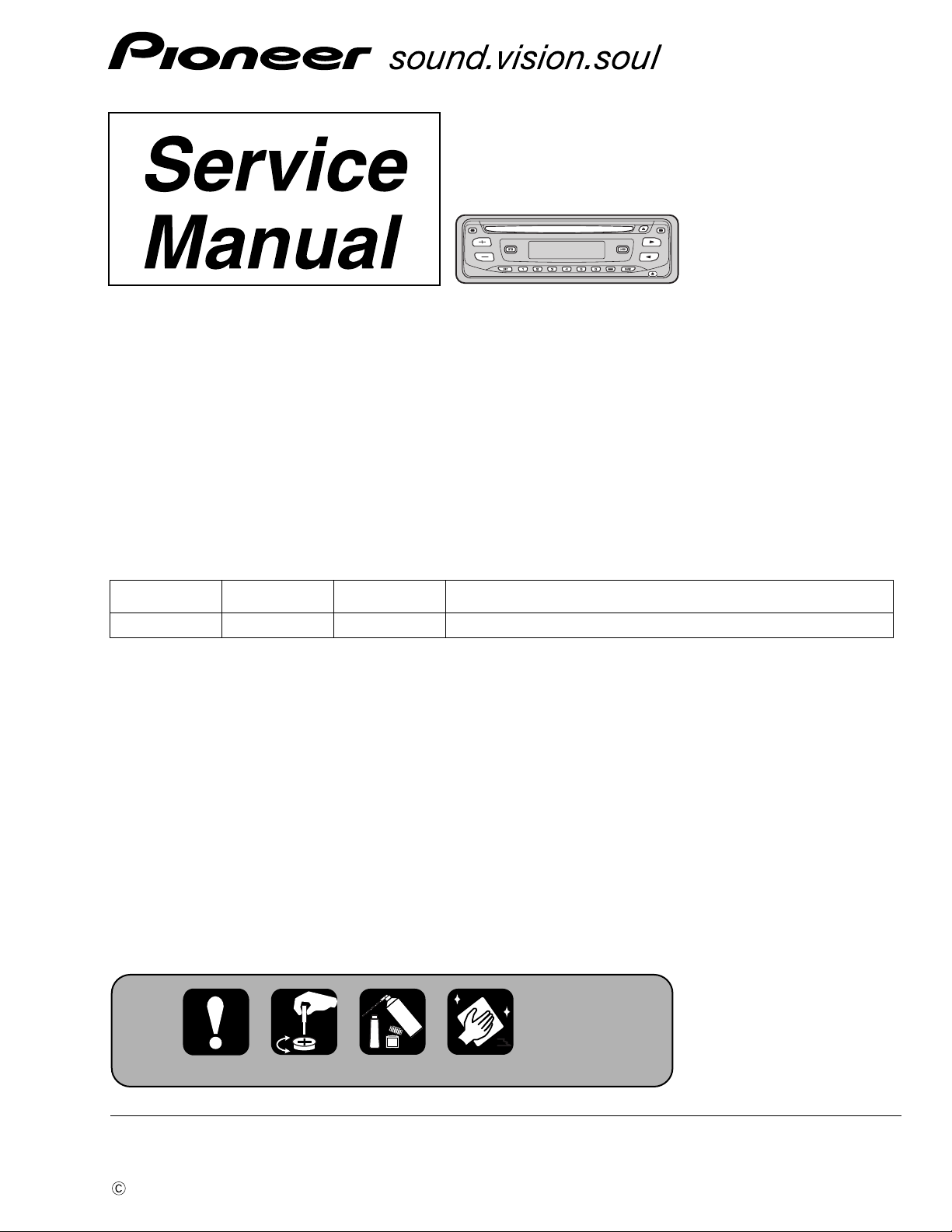
DEH-1750/XN/GS
HIGH POWER CD PLAYER WITH FM/AM TUNER
DEH-1750
DEH-1770
This service manual should be used together with the following manual(s):
Model No. Order No. Mech.Module Remarks
CX-3110 CRT3178 S10.1 CD Mech. Module:Circuit Description, Mech. Description, Disassembly
/XN/CS
/XN/GS
For details, refer to "Important Check Points for Good Servicing".
K-ZZW. OCT. 2004 printed in Japan
Page 2
1234
SAFETY INFORMATION
This service manual is intended for qualified service technicians; it is not meant for the casual do-it-yourselfer.
Qualified technicians have the necessary test equipment and tools, and have been trained to properly and safely
A
repair complex products such as those covered by this manual.
Improperly performed repairs can adversely affect the safety and reliability of the product and may void the warranty.
If you are not qualified to perform the repair of this product properly and safely, you should not risk trying to do so
and refer the repair to a qualified service technician.
- Service Precaution
1. You should conform to the regulations governing the product (safety, radio and noise, and other
B
regulations), and should keep the safety during servicing by following the safety instructions
described in this manual.
2. Before disassembling the unit, be sure to turn off the power. Unplugging and plugging the connectors
during power-on mode may damage the ICs inside the unit.
3. To protect the pickup unit from electrostatic discharge during servicing, take an appropriate treatment
(shorting-solder) by referring to "the DISASSEMBLY".
4. After replacing the pickup unit, be sure to check the grating.
C
D
E
F
2
1234
DEH-1750/XN/GS
Page 3
5678
[Important Check Points for Good Servicing]
In this manual, procedures that must be performed during repairs are marked with the below symbol.
Please be sure to confirm and follow these procedures.
1. Product safety
Please conform to product regulations (such as safety and radiation regulations), and maintain a safe servicing environment by
following the safety instructions described in this manual.
1 Use specified parts for repair.
Use genuine parts. Be sure to use important parts for safety.
2 Do not perform modifications without proper instructions.
Please follow the specified safety methods when modification(addition/change of parts) is required due to interferences such as
radio/TV interference and foreign noise.
3 Make sure the soldering of repaired locations is properly performed.
When you solder while repairing, please be sure that there are no cold solder and other debris.
Soldering should be finished with the proper quantity. (Refer to the example)
4 Make sure the screws are tightly fastened.
Please be sure that all screws are fastened, and that there are no loose screws.
5 Make sure each connectors are correctly inserted.
Please be sure that all connectors are inserted, and that there are no imperfect insertion.
6 Make sure the wiring cables are set to their original state.
Please replace the wiring and cables to the original state after repairs.
In addition, be sure that there are no pinched wires, etc.
7 Make sure screws and soldering scraps do not remain inside the product.
Please check that neither solder debris nor screws remain inside the product.
8 There should be no semi-broken wires, scratches, melting, etc. on the coating of the power cord.
Damaged power cords may lead to fire accidents, so please be sure that there are no damages.
If you find a damaged power cord, please exchange it with a suitable one.
9 There should be no spark traces or similar marks on the power plug.
When spark traces or similar marks are found on the power supply plug, please check the connection and advise on secure
connections and suitable usage. Please exchange the power cord if necessary.
0 Safe environment should be secured during servicing.
When you perform repairs, please pay attention to static electricity, furniture, household articles, etc. in order to prevent injuries.
Please pay attention to your surroundings and repair safely.
A
B
C
D
2. Adjustments
To keep the original performance of the products, optimum adjustments and confirmation of characteristics within specification.
Adjustments should be performed in accordance with the procedures/instructions described in this manual.
3. Lubricants, Glues, and Replacement parts
Use grease and adhesives that are equal to the specified substance.
Make sure the proper amount is applied.
4. Cleaning
For parts that require cleaning, such as optical pickups, tape deck heads, lenses and mirrors used in projection monitors, proper
cleaning should be performed to restore their performances.
5. Shipping mode and Shipping screws
To protect products from damages or failures during transit, the shipping mode should be set or the shipping screws should be
installed before shipment. Please be sure to follow this method especially if it is specified in this manual.
56
DEH-1750/XN/GS
E
F
7
8
3
Page 4

1234
CONTENTS
SAFETY INFORMATION..................................................................................................................................... 2
1. SPECIFICATIONS ............................................................................................................................................5
2. EXPLODED VIEWS AND PARTS LIST............................................................................................................8
A
B
C
2.1 PACKING................................................................................................................................................... 8
2.2 EXTERIOR............................................................................................................................................... 10
2.3 CD MECHANISM MODULE.....................................................................................................................12
3. BLOCK DIAGRAM AND SCHEMATIC DIAGRAM..........................................................................................14
3.1 BLOCK DIAGRAM................................................................................................................................... 14
3.2 OVERALL CONNECTION DIAGRAM(GUIDE PAGE)..............................................................................16
3.3 KEYBOARD UNIT.................................................................................................................................... 22
3.4 CD MECHANISM MODULE.....................................................................................................................24
4. PCB CONNECTION DIAGRAM ..................................................................................................................... 28
4.1 TUNER AMP UNIT...................................................................................................................................28
4.2 KEYBOARD UNIT.................................................................................................................................... 32
4.3 CD CORE UNIT(S10) ..............................................................................................................................34
5. ELECTRICAL PARTS LIST ............................................................................................................................ 36
6. ADJUSTMENT ...............................................................................................................................................39
6.1 CD ADJUSTMENT................................................................................................................................... 39
6.2 CHECKING THE GRATING AFTER CHANGING THE PICKUP UNIT.................................................... 41
6.3 ERROR MODE ........................................................................................................................................43
6.4 SYSTEM MICROCOMPUTER TEST PROGRAM...................................................................................44
7. GENERAL INFORMATION.............................................................................................................................45
7.1 DIAGNOSIS............................................................................................................................................. 45
7.1.1 DISASSEMBLY .....................................................................................................................................45
7.1.2 CONNECTOR FUNCTION DESCRIPTION.......................................................................................... 48
7.2 PARTS......................................................................................................................................................49
7.2.1 IC ..........................................................................................................................................................49
7.2.2 DISPLAY............................................................................................................................................... 56
7.3 OPERATIONAL FLOW CHART ...............................................................................................................57
7.4 CLEANING............................................................................................................................................... 58
8. OPERATIONS ................................................................................................................................................ 59
D
E
F
4
1234
DEH-1750/XN/GS
Page 5
5678
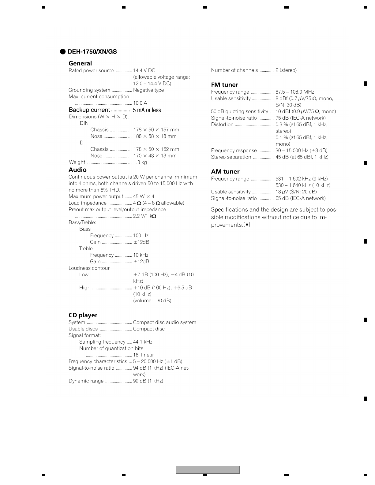
1. SPECIFICATIONS
A
B
C
D
E
56
DEH-1750/XN/GS
F
7
8
5
Page 6
1234
A
B
C
D
E
F
6
1234
DEH-1750/XN/GS
Page 7

5678
A
B
C
D
E
56
DEH-1750/XN/GS
F
7
8
7
Page 8
N
5
8
3
1234
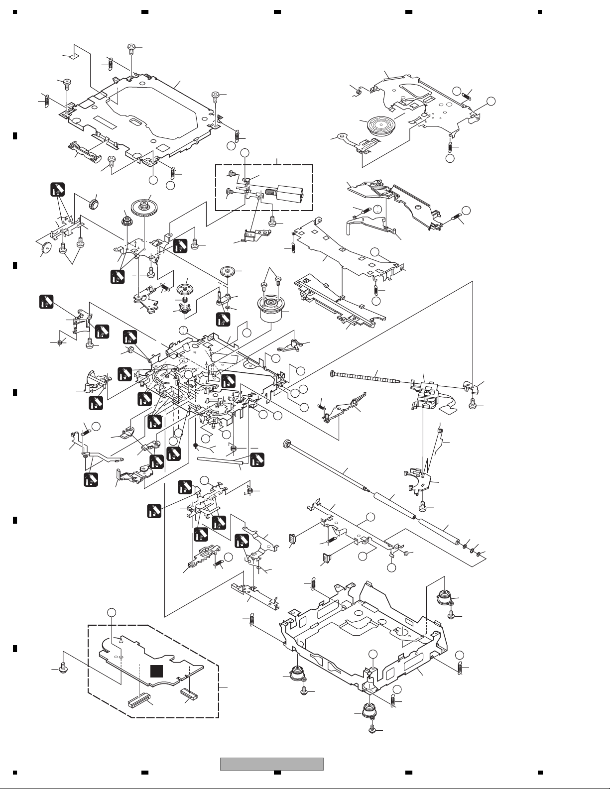
2. EXPLODED VIEWS AND PARTS LIST
OTES : • Parts marked by " * " are generally unavailable because they are not in our Master Spare Parts List.
• The > mark found on some component parts indicatesthe importance of the safety factor of the part.
A
Therefore, when replacing, be sure to use parts of identical designation.
• Screw adjacent to mark on the product are used for disassembly.
• For the applying amount of lobricants or glue, follow the instructions in this manual.
(In the case of no amount instructions,apply as you think it appropriate.)
2.1 PACKING
"
B
C
D
1
E
F
8
1234
DEH-1750/XN/GS
Page 9
5678
PACKING SECTION PARTS LIST
Mark No. Description Part No.
1 Accessory Assy CEA4850
2 Screw Assy CEA3849
3 Screw CBA1650
* 4 Polyethylene Bag CEG-127
5 Screw CRZ50P090FTC
6 Screw TRZ50P080FTC
* 7 Polyethylene Bag CEG-158
8 Handle CNC5395
9 Bush CNV3930
10 Polyethylene Bag CEG-162
11 Carton(DEH-1750) CHG5418
Carton(DEH-1770) CHG5419
Owner's Manual,Installation Manual
Part No. Language
CRD3910 English, Traditional Chinese, Arabic
CRD3911 English, Traditional Chinese, Arabic
CRD3912 English, Spanish, Portuguese(B)
CRD3913 English, Spanish, Portuguese(B)
Mark No. Description Part No.
12 Contain Box(DEH-1750) CHL5347
Contain Box(DEH-1770) CHL5348
13 Protector CHP2664
14 Protector CHP2868
15-1 Owner's Manual(DEH-1750) CRD3910
Owner's Manual(DEH-1770) CRD3912
15-2 Installation Manual(DEH-1750) CRD3911
Installation Manual(DEH-1770) CRD3913
15-3 Caution Card CRP1310
16 Case Assy CXB3520
17 Cord Assy XDE7008
A
B
C
D
E
F
56
DEH-1750/XN/GS
7
8
9
Page 10
1234
2.2 EXTERIOR
A
B
C
D
E
F
10
1234
DEH-1750/XN/GS
Page 11

5678
EXTERIOR SECTION PARTS LIST
Mark No. Description Part No.
1 Screw BSZ26P060FTC
2 Screw BSZ26P100FTC
3 Cable CDE7702
4 Cord Assy XDE7008
5 Panel CNS8048
6 Case CNB2793
7 Holder CNC8659
8 Insulator CNM9145
9 Tuner Amp Unit(DEH-1750) CWM9601
Tuner Amp Unit(DEH-1770) CWM9605
10 Screw ASZ26P060FTC
11 Screw BMZ26P160FTC
12 Screw BPZ26P080FTC
> 13 Fuse(10A) CEK1208
14 Pin Jack(CN352) CKB1059
15 Plug(CN901) CKM1376
16 Connector(CN831) CKS3581
17 Connector(CN651) CKS3835
18 Antenna Jack(CN401) CKX1056
19 Holder CND2413
20 Holder CND2414
21 Heat Sink CNR1762
22 FM/AM Tuner Unit CWE1912
23 Holder CND1054
24 Terminal(CN402) VNF1084
Mark No. Description Part No.
47 Spring CBH2367
48 Bracket CNC6791
49 Holder CNC8042
50 Cover CNM6276
51 Panel CNS8044
52 Arm CNV4692
53 Arm CNV4728
54 Arm CNV5576
55 Screw IMS20P030FZK
56 Chassis Unit CXC3600
57 CD Mechanism Module(S10) CXK5605
58 Screw ISS26P055FTC
59 IC(IC302) TDA7386
60 Transistor(Q921,991) 2SD2396
A
B
C
25 Detach Grille Assy(DEH-1750) CXC3538
Detach Grille Assy(DEH-1770) CXC3542
26 Screw BPZ20P100FZK
27 Button(VOLUME) CAC8924
28 Button(SELECT) CAC8925
29 Button(BTB,SRC) CAC8927
30 Button(LOUD,BAND) CAC8928
31 Button(1-6) CAC8929
32 Button(CD EJECT,AUDIO) CAC8930
33 Button(DETACH) CAC8931
34 Spring CBH2210
35 Cover CNS8042
36 LCD CAW1847
37 Connector(CN1801) CKS3580
38 Holder CND2412
39 Sheet CNM9144
40 Lighting Conductor CNV8190
41 Rubber CNV8191
42 Connector CNV8192
43 Grille Unit(DEH-1750) CXC3592
Grille Unit(DEH-1770) CXC3994
44 Button CAC4836
45 Spring CBH1835
46 Spring CBH2208
D
E
F
56
DEH-1750/XN/GS
7
8
11
Page 12
1234
2.3 CD MECHANISM MODULE
42
A
5
13
13
5
81
34
5
15
22
E
F
93
13
A
44
B
5
B
1
54
53
C
52
13
D
86
86
82
83
4
37
71
4
29
51
1
73
50
72
10
1
I
76
B
55
5
36
4
1
18
2
64
47
C
24
2
1
7
61
2
M
1
23
87
75
E
63
57
62
58
1
G
L
1
N
R
1
1
2
1
40
56
D
O
16
P
1
33
1
P
19
J
12
3
20
39
1
69
30
2
21
M
D
79
2
1GEM1024
2GEM1045
3GEM1035
E
92
26
G
68
28
I
H
28
45
J
38
23
K
59
49
F
Q
A
27
H
77
90
48
8
67
17
78
25
70
60
80
N
L
K
43
46
6
60
11
89
10
14
74
R
31
41
85
C
91
F
C
65
1
2
3
85
66
35
O
31
Q
14
85
12
1234
DEH-1750/XN/GS
Page 13

5678
CD MECHANISM MODULE SECTION PARTS LIST
Mark No. Description Part No.
1 CD Core Unit(S10) CWX3110
2 Connector(CN101) CKS4182
3 Connector(CN701) CKS4188
4 Screw BMZ20P035FTC
5 Screw BSZ20P040FTC
6 Screw(M2x4) CBA1362
7 Screw(M2x3) CBA1824
8 Screw(M2x3) CBA1825
9 •••••
10 Washer CBF1038
11 Washer CBF1060
12 Spring CBH2390
13 Spring CBH2606
14 Spring CBH2607
15 Spring CBH2608
16 Spring CBH2609
17 Spring CBH2610
18 Spring CBH2735
19 Spring CBH2612
20 Spring CBH2613
21 Spring CBH2614
22 Spring CBH2615
23 Spring CBH2616
24 Spring CBH2617
25 Spring CBH2620
26 Spring CBH2621
27 Spring CBH2641
28 Spring CBH2642
29 Spring CBH2643
30 Spring CBH2659
31 Spring CBH2688
32 •••••
33 Shaft CLA4441
34 Frame CNC9962
35 Frame CNC9963
36 Bracket CND2712
37 Bracket CND1895
38 Arm CNC9968
39 Arm CND1909
40 Lever CND2032
41 Lever CNC9984
42 Sheet CNM8134
43 Collar CNV7798
44 Guide CNV7799
45 Arm CNV8403
Mark No. Description Part No.
50 Gear CNV8379
51 Gear CNV8380
52 Gear CNV8381
53 Gear CNV8382
54 Gear CNV8383
55 Gear CNV8384
56 Rack CNV8385
57 Arm CNV8386
58 Arm CNV8387
59 Guide CNV8388
60 Roller CNV7218
61 Gear CNV8389
62 Arm CNV8391
63 Arm CNV8390
64 Arm CNV8392
65 Damper CNV7313
66 Damper CNV7314
67 Arm CNV8394
68 Arm CNV8395
69 Guide CNV8396
70 Guide CNV8397
71 Holder CNV8398
72 Arm CNV8402
73 Gear CNV8400
74 Damper CNV7618
75 Motor Unit(M1) CXC4440
76 Chassis Unit CXC2318
77 Screw Unit CXB8729
78 Gear Unit CXC2397
79 Arm Unit CXC2316
80 Arm CND1896
81 Arm CND1894
82 Motor Unit(M2) CXB8933
83 Bracket CNC9985
84 •••••
85 Screw(M2x5) EBA1028
86 Screw JFZ20P020FTC
87 Screw JGZ17P022FTC
88 •••••
89 Washer YE20FTC
90 Pickup Unit(P10)(Service) CXX1641
91 Screw IMS26P030FTC
92 Spring CBL1635
93 Clamper CNV8372
A
B
C
D
E
46 Rack CNV8374
47 Holder CNV8376
48 Holder CNV8377
49 Arm CNV8378
56
DEH-1750/XN/GS
F
7
8
13
Page 14
Q
Q
Q
1234
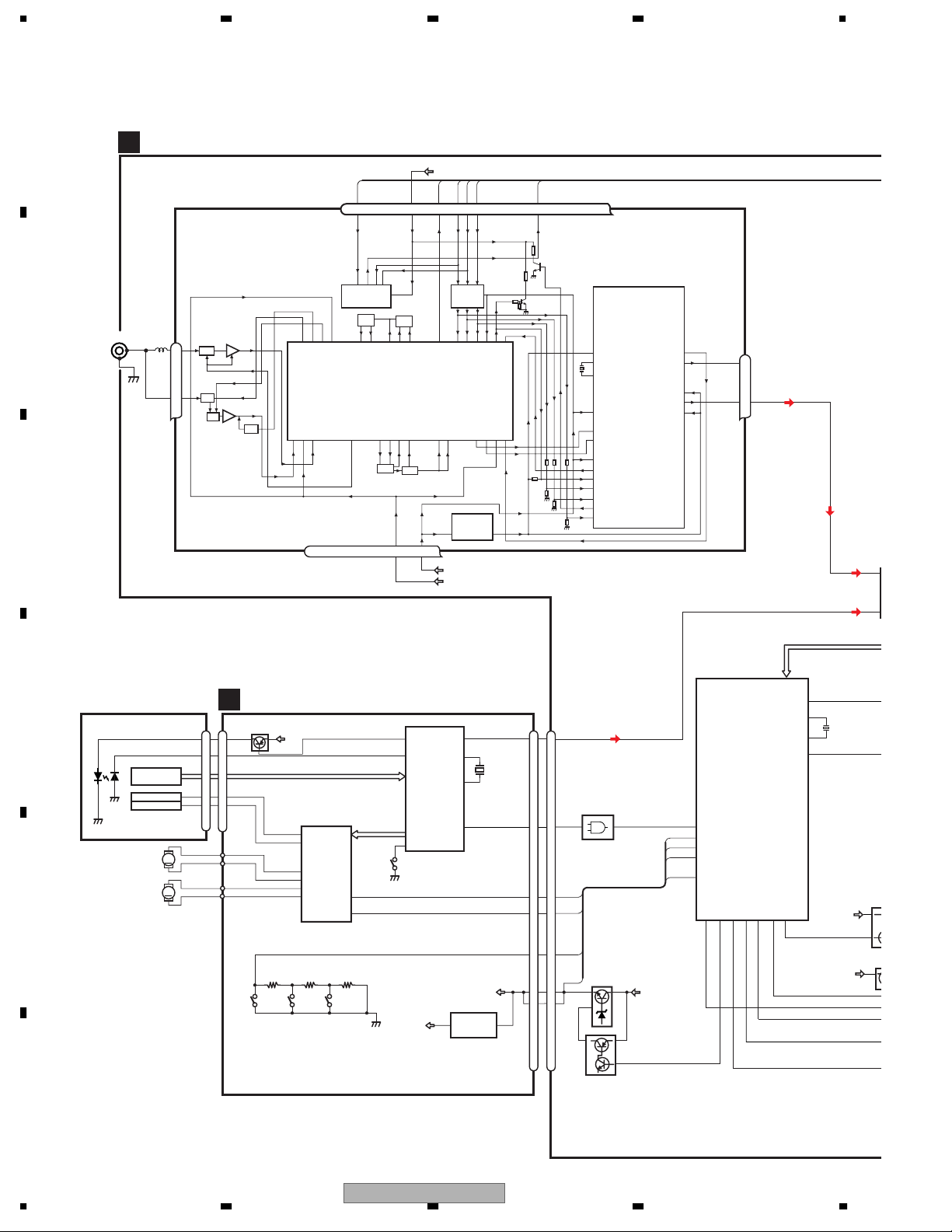
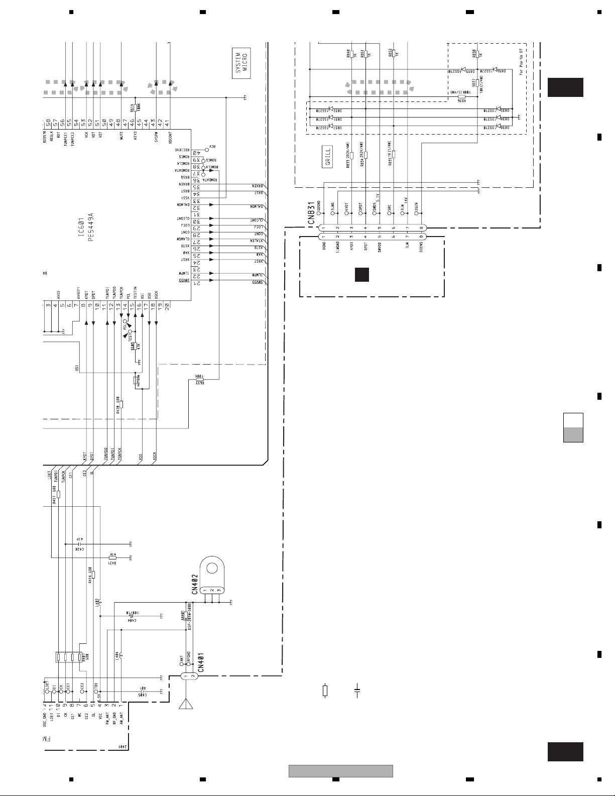
3. BLOCK DIAGRAM AND SCHEMATIC DIAGRAM
3.1 BLOCK DIAGRAM
A
TUNER AMP UNIT
A
VDD
FM/AM TUNER UNIT
B
ANTENNA
CN401
1
2
1
3
AM ANT
FM ANT
ATT
ATT
ANT adj
FMRF
FMRF
RF adj
7 6 13 5 10 9 8 11 14 18 19 20 21
NC
CE2
ROM_VDD
IC 3 EEPROM
5.0V
OSC
LPF
IC 1
3.3V
MIXER, IF AMP
T51
CF52
C
RFGND
OSCGND
DGND
212 1522 16 4 17
AUDIOGNDNCVCC
VDD_3.3
3.3V
SL
TUN 3V
VCC
DI
IC 5
←
5V 3.3V
IC 4
3.3V 2.5V
CK
NC
CE1
←
2.5V
DO
NCNCNC
NC
DET, FM MPX,
RDS DECODER
Rch
IC 2
2.5V
24
Lch
23
TUN L
2
CD L
VST,VCK,VDT
3
PICKUP UNIT
D
(P10)(SERVICE)
LASER
DIODE
HOLOGRAM
UNIT
FOCUS ACT.
TRACKING ACT.
MONITOR
DIODE
SPINDLE
MOTOR
CARRIAGE
LOADING/
MOTOR
LD+
MD
FOP
TOP
M
M
E
CD CORE UNIT(S10)
C
D
CN101
Q101
14
5
FOP
1
TOP
4
12EJ 8EJ DSCSNS
3R3V
12
13
16
15
17
18
FOP
TOP
ACT,MOTOR
DRIVER
SOP
SOM
LCOM
LCOP
LOEJ
CONT
IC 301
BA5835FP
AC, F, E, BD
FD, TD, SD, MD
22
9
HOME
1
LD
2
PD
SERVO
CONTROL,
DSP,
LPF, DAC
IC 201
UPD63712AGC
42
LIMIT
3R3V
20
LOUT
23
xtal
X201
24
XTAL
12
SO
VD
3.3V REGULATOR
3
IC 701
CN701
LOUT
CONT
DSCSNS
1
LOEJ
CN651
8
14
SYSTEM CONTROLLER
XSI
LOEJ
CONT
DISCSENS
VDSENS
INTRQ
66
41
VDCONT
8
IC 601(2/2)
PE5449A
KYDT
DSENS
9
65
DPDT
21
XSI
16
5
7
6
VD
1
2
IC 652
24
6
TC7SET08FU
17
15
16
VDSENS
20
21
Q991
Q992
B.UP
16
29
28
79
78
swvdd
22
MUTE
SYSPW
ILMPW
48
70
X1
X601
69
X2
43
B.UP
VDD
NJM2885DL1-33
F
14
1234
DEH-1750/XN/GS
Page 15
5678
A
RESET
CE2
55
TUNPCE2
CE1
56
TUNPCE1
DO
11
TUNPDI
DI
12
TUNPDO
CK
13
TUNPCK
76
SL
1
S-80834CNY
60
reset
SYSTEM CONTROLLER
IC 601(1/2)
PE5449A
IC 961
2
DALMON
bsens
asens
ANTPW
VDD
RCA OUT
CN352
RL
VDD REGULATOR
VDD
32
64
63
49
Q911
BACKUP SENSE
Q931
ACC SENSE
Q912
B.UP
B.UP
ACC
B REMOTE
TPD1018F
IC 551
6
15
Q352
CN901
2
FUSE
16
10A
14
11
15 15
RL
B
16
14
11
BACK UP
ACC
B.REM
GND
C
TE
X1
X2
W
CD L
VST,VCK,VDT
48
70
69
43
TUN L
X601
B.UP
VDD
ELECTRONIC VOLUME/
SOURCE SELECTOR
2
IN1-L
IC 151
PML010A
3
IN2-L
CN831
Q821
ILM
7
Q822
Q801
SWVDD
5
SOURCE
66
DPDT
4
DSENS
KYDT
3
FL
RL
CN1801
7
5
4
88
KYDT
3
10
11
ILL
SW5V
SOURCE
DPDT
DSENS
MUTE
Q452
SOURCE
18
DPDT
20
KTDT
10
56
VDD
VLCD
LCD DRIVER/
KEY CONTROLLER
PD6340A
IC 1801
14
12
KEY DATA
POWER AMP
IC 302
FLIN
TDA7386
RLIN
STBYMUTE
22 4
SYS 8.4V REGULATOR
VCC
TUNER 3.3V REGULATOR
TUN 3V
Q921
IC 901
BA33BC0FP
6,20
FLFL+
RLRL+
Q923
B.UP
23
21
3
5
SYSPW
31
VCC
KEYBOARD UNIT
B
KEY MATRIX
LCD
B.UP
7
7
5
5
8
8
6
6
FLFL+
RL-
RL+
D
E
56
DEH-1750/XN/GS
F
7
8
15
Page 16
1234
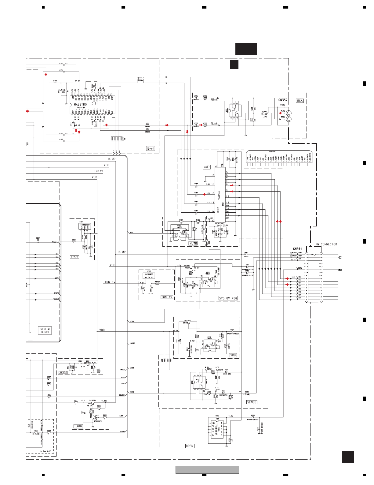
3.2 OVERALL CONNECTION DIAGRAM(GUIDE PAGE)
Note: When ordering service parts, be sure to refer to " EXPLODED VIEWS AND PARTS LIST" or
"ELECTRICAL PARTS LIST".
A
A-a
C
A-a A-b
A-a
A-b
Large size
SCH diagram
Guide page
CN701
A-b
Detailed page
CD:+0.4dBs
A-a
B
FM:-20.4dBs
AM:-31.3dBs
C
D
ANTENNA
E
NOTE :
Symbol indicates a resistor.
No differentiation is made between chip resistors and
discrete resistors.
Symbol indicates a capacitor.
No differentiation is made between chip capacitors and
discrete capacitors.
The > mark found on some component parts indicates
the importance of the safety factor of the part.
Therefore, when replacing, be sure to use parts of
identical designation.
Decimal points for resistor
and capacitor fixed values
are expressed as :
←
2.2 2R2
←
0.022 R022
B
CN1801
F
16
A
DEH-1750/XN/GS
1234
Page 17
4
5678
A
A-b
TUNER AMP UNIT
A
dBs
FM: +2.8dBs
AM: -8.1dBs
CD:+10.6dBs
>
REAR L
REAR R
FM:+2.0dBs
AM: -8.9dBs
CD:+9.8dBs
B
C
>
CEK1208
10A
BACKUP
GND
ACC
B.REM
RL–
FM:+29.3dBs
AM:+18.4dBs
CD:+36.6dBs
FL–
RL+
FL+
RR–
FR–
RR+
FR+
D
56
DEH-1750/XN/GS
E
F
A
7
8
17
Page 18
A
A-b
1234
1
CD:+0.4dBs
2 3 4
B
CN701
C
C
A-b
A-a
A-a
D
E
F
A-a
18
FM:-20.4dBs
AM:-31.3dBs
1234
DEH-1750/XN/GS
Page 19
5678
3 4 5
A
6
A-b
B
B
CN1801
←
←
Decimal points for resistor
and capacitor fixed values
are expressed as :
2.2 2R2
0.022 R022
A-b
A-a
A-a
C
D
E
Symbol indicates a resistor.
No differentiation is made between chip resistors and
discrete resistors.
Symbol indicates a capacitor.
No differentiation is made between chip capacitors and
discrete capacitors.
NOTE :
ANTENNA
DEH-1750/XN/GS
56
The > mark found on some component parts indicates
the importance of the safety factor of the part.
Therefore, when replacing, be sure to use parts of
identical designation.
A-a
7
8
F
19
Page 20

1234
GND
ACC
B.REM
>
BACKUP
10A
CEK1208
A
FM:+2.0dBs
CD:+9.8dBs
AM: -8.9dBs
REAR L
REAR R
B
>
TUNER AMP UNIT
A
C
A-b
A-a
FM: +2.8dBs
CD:+10.6dBs
D
E
AM: -8.1dBs
F
A-b
20
1
Bs
2 3 4
DEH-1750/XN/GS
1234
Page 21

>
BACKUP
10A
CEK1208
5678
FR–
FL–
RL+
B.REM
RL–
GND
ACC
FR+
FL+
RR+
RR–
A
FM:+29.3dBs
CD:+36.6dBs
AM:+18.4dBs
B
A-b
A-a
C
D
E
3 4 5
56
DEH-1750/XN/GS
F
6
7
8
A-b
21
Page 22

1234
3.3 KEYBOARD UNIT
A
B
C
D
E
F
B
22
1234
DEH-1750/XN/GS
Page 23

5678
A
KEYBOARD UNIT
B
B
A
CN831
CEL1651 (GREEN)
CEL1651 (GREEN)
CL-490S-WF-SD
D1803-D1809 : SML-310PT
C
D
E
56
DEH-1750/XN/GS
F
B
7
8
23
Page 24

1234
3.4 CD MECHANISM MODULE
A
PICKUP UNIT(P10)(SERVICE)
#
B
F
T
T
F F
T
T
F
F
F
T
T
F
T
T
F
F
F
T
T
!
C
0
1
9
D
MOTOR DRIVER
8
T
7
F
C
M1
CXC4440
SPINDLE MOTOR
E
M2
CXB8933
LOADING/CARRIAGE
MOTOR
S
S
C
C
3.3V
REGULATOR
F
F
T
T
@
S
5
6
3
C
C
S
S
F
24
C
DEH-1750/XN/GS
1234
Page 25

5678
A
F
T
C
S
SWITCHES:
CD CORE UNIT(S10)
S901:HOME SWITCH..........ON-OFF
S903:DSCSNS SWITCH......ON-OFF
S904:12EJ SWITCH.............ON-OFF
S905:8EJ SWITCH...............ON-OFF
The underlined indicates the switch position.
B
@
9
RF AMP / SERVO / DSP
DAC / LPF
4
SIGNAL LINE
F
FOCUS SERVO LINE
T
TRACKING SERVO LINE
C
CARRIAGE SERVO LINE
S
SPINDLE SERVO LINE
CD CORE UNIT(S10)
C
2
A
CN651
7.5V
7.5V
C
D
5
6
E
3
$
%
C
C
F
C
56
DEH-1750/XN/GS
7
8
25
Page 26

1234
- Waveforms Note : 1. The encircled numbers denote measuring points in the circuit diagram.
2. Reference voltage REFO1(1.65V)
1 DSCSNS
A
2 CLCONT
3 LOEJ
4 VD
When loading a 12cm CD
5V/div
5V/div
5V/div
10V/div
500ms/div
1 DSCSNS
2 CLCONT
3 LOEJ
4 VD
When loading an 8cm CD
5V/div
5V/div
5V/div
10V/div
500ms/div
5 SIN
6 CIN
7 TIN
When setting up after loading a 12cm CD-DA
disc
1V/div
500mV/div
500mV/div
2s/div
Ref.:
GND
Mode:
Normal
B
8 FIN
9 RFOK
5 SIN
200mV/div
2V/div
2V/div
500ms/div
Ref.:
GND
Mode:
Normal
0 TE
! FE
500mV/div
500mV/div
200ms/div
Ref.:
REFO
Mode:
Normal
! FE
8 FIN
0 TE
7 TIN
When setting up "Source On"(12cm CD-DA) During "Play"(CD-DA)
Ref.:
REFO
C
Mode:
Normal
@ MDX
5 SIN
500mV/div
1V/div
5ms/div
When setting up "Source On"
Ref.:
REFO
Mode:
Normal
@ MDX
5 SIN
500mV/div
1V/div
5µs/div
Ref.:
REFO
Mode:
Normal
# RFAGC 500mV/div 0.5µs/div
500mV/div
500mV/div
500mV/div
500mV/div
20ms/div
Spindle waveform during "Play"
D
Ref.:
REFO
Mode:
Normal
8 FIN
! FE
E
Focus Search
Ref.:
REFO
Mode:
TEST
F
500mV/div
500mV/div
200ms/div
Spindle waveform during "Play"(Magnified) RF eye pattern
Ref.:
REFO
Mode:
Normal
0 TE
# RFAGC
500mV/div
500mV/div
2ms/div
Ref.:
REFO
Mode:
Normal
# RFAGC
0 TE
7 TIN
When "Tracking Open" 1 Track Jump
Ref.:
REFO
Mode:
TEST
Ref.:
REFO
Mode:
TEST
1V/div
500mV/div
500mV/div
500µs/div
26
1234
DEH-1750/XN/GS
Page 27

5678
# RFAGC
0 TE
7 TIN
32 Track Jump
Ref.:
REFO
Mode:
TEST
# RFAGC
0 TE
6 CIN
5 SIN
When reproducing scratch(1mm)
Ref.:
REFO
Mode:
Normal
1V/div
500mV/div
500mV/div
1V/div
1V/div
500mV/div
2V/div
500ms/div
500µs/div
# RFAGC
0 TE
7 TIN
1V/div
500mV/div
500mV/div
5ms/div
# RFAGC
7 TIN
0 TE
8 FIN
100(32x3) Track Jump When reproducing black dots(1mm)
Ref.:
REFO
Mode:
TEST
# RFAGC
0 TE
6 CIN
5 SIN
When reproducing fingerprint(65µm)
Ref.:
REFO
Mode:
Normal
1V/div
1V/div
500mV/div
2V/div
5ms/div
Ref.:
REFO
Mode:
Normal
# RFAGC
0 TE
6 CIN
5 SIN
During inside/outside search
(outer circumference → inner circumference)
Ref.:
REFO
Mode:
Normal
1V/div
1V/div
1V/div
1V/div
1V/div
1V/div
500mV/div
2V/div
500µs/div
500µs/div
A
B
C
$ LOUT
% ROUT
Analog Audio
Ref.:
AGND
Mode:
Normal
1V/div
1V/div
200µs/div
1 DSCSNS
2 CLCONT
3 LOEJ
When "Eject"(12cm CD) When "Eject"(8cm CD)
Ref.:
GND
Mode:
Normal
5V/div
5V/div
5V/div
200ms/div
1 DSCSNS
2 CLCONT
3 LOEJ
Ref.:
GND
Mode:
Normal
5V/div
5V/div
5V/div
200ms/div
D
E
56
DEH-1750/XN/GS
F
7
8
27
Page 28

1234
4. PCB CONNECTION DIAGRAM
4.1 TUNER AMP UNIT
A
B
C
NOTE FOR PCB DIAGRAMS
1.The parts mounted on this PCB
include all necessary parts for
several destination.
For further information for
respective destinations, be sure
to check with the schematic dia gram.
2.Viewpoint of PCB diagrams
Connector
P.C.Board
Capacitor
Chip Part
SIDE A
SIDE B
TUNER AMP UNIT
A
Cord Assy
D
E
F
C
CN701
B
CN1801
28
A
DEH-1750/XN/GS
1234
Page 29

5678
RCA
ANTENNA
2
1
SIDE A
A
B
C
B
CN1801
FRONT
FM/AM TUNER UNIT
D
E
F
56
DEH-1750/XN/GS
A
7
8
29
Page 30

1234
A
TUNER AMP UNIT
A
B
1
C
D
E
F
A
30
1234
DEH-1750/XN/GS
Page 31

5678
SIDE B
A
B
C
D
E
F
56
DEH-1750/XN/GS
A
7
8
31
Page 32

1234
4.2 KEYBOARD UNIT
KEYBOARD UNIT
B
A
AUDIO
RIGHT
EJECT
B
C
LEFT
LOUD
LOC BAND
SIDE A
456
D
VOL+
BTB
VOL-
E
3
SRC 1 2
CLK
F
B
32
1234
DEH-1750/XN/GS
Page 33

5678
KEYBOARD UNIT
B
SIDE B
A
B
C
A
CN831
D
E
F
56
DEH-1750/XN/GS
B
7
8
33
Page 34

1234
4.3 CD CORE UNIT(S10)
CD CORE UNIT(S10)
C
A
M2
B
C
LOADING
/CARRIAGE
MOTOR
M1
SPINDLE
MOTOR
SIDE A
A
CN651
D
PICKUP UNIT(P10)(SERVICE)
E
HOME
REFO1
F
E
F
C
34
1234
DEH-1750/XN/GS
Page 35

5678
CD CORE UNIT(S10)
C
DSCSNS
8EJ
SIDE B
A
12EJ
B
C
321
D
E
56
DEH-1750/XN/GS
F
C
7
8
35
Page 36

1234
5. ELECTRICAL PARTS LIST
NOTE:
A
• Parts whose parts numbers are omitted are subject to being not supplied.
• The part numbers shown below indicate chip components.
Chip Resistor
RS1/_S___J,RS1/__S___J
Chip Capacitor (except for CQS.....)
CKS....., CCS....., CSZS.....
• The > mark found on some component parts indicatesthe importance of the safety factor of the part.
Therefore, when replacing, be sure to use parts of identical designation.
B
Circuit Symbol and No. Part No.
A
Unit Number:CWM9601(DEH-1750)
Unit Number:CWM9605(DEH-1770)
Unit Name:Tuner Amp Unit
MISCELLANEOUS
IC 151 (B,134,85) IC PML010A
IC 302 (A,95,135) IC TDA7386
C
IC 551 (B,62,118) IC TPD1018F
IC 601 (B,88,62) IC PE5449A
IC 652 (B,113,45) IC TC7SET08FU
IC 901 (B,144,29) IC BA33BC0FP
IC 961 (A,59,81) IC S-80834CNY
Q 352 (B,162,129) Transistor UMH3N
Q 452 (B,140,128) Transistor UMD2N
Q 801 (B,84,26) Transistor 2SA1036K
Q 821 (B,43,16) Transistor 2SA1036K
Q 822 (B,32,18) Transistor DTC114EU
D
Q 912 (B,15,145) Transistor UMD2N
Q 913 (A,16,111) Transistor 2SD1859
Q 921 (A,9,104) Transistor 2SD2396
Q 923 (B,26,79) Transistor UMD2N
Q 931 (B,62,107) Transistor UMX1N
Q 991 (A,9,69) Transistor 2SD2396
Q 992 (B,23,58) Transistor UMD2N
D 551 (A,63,126) Diode MPG06G-6415G3
D 552 (A,60,126) Diode MPG06G-6415G3
D 831 (A,110,21) Diode 1SS270
D 832 (A,113,21) Diode 1SS270
E
D 833 (A,118,21) Diode 1SS270
D 834 (A,110,13) Diode 1SS270
D 835 (A,113,13) Diode 1SS270
D 836 (A,118,13) Diode 1SS270
D 837 (A,115,21) Diode 1SS270
D 838 (A,115,13) Diode 1SS270
D 901 (A,36,132) Diode MPG06G-6415G3
D 902 (A,36,129) Diode MPG06G-6415G3
D 911 (A,20,107) Diode MPG06G-6415G3
D 912 (A,15,129) Diode HZS6L(B2)
D 921 (A,25,88) Diode HZS9L(B3)
F
D 931 (A,70,116) Diode HZS7L(C3)
D 932 (A,53,113) Diode HZS7L(A1)
D 991 (A,21,66) Diode HZS7L(C3)
Circuit Symbol and No. Part No.
L 151 (A,146,70) Inductor LAU2R2K
L 401 (A,158,58) Inductor LAU2R2K
L 402 (A,147,95) Inductor LAU2R2K
L 404 (B,161,101) Inductor LCTAW4R7J2520
L 601 (A,94,85) Ferri-Inductor LAU100K
L 602 (A,105,67) Inductor LAU2R2K
L 801 (A,94,25) Inductor LAU2R2K
L 901 (A,37,108) Choke Coil 600µH CTH1280
X 601
FU352 (B,144,135) Fuse 3A CEK1286
AR401 (A,162,110) Surge Protector DSP-201M-S00B
>
(A,104,72) Radiator 12.58291MHz
Fuse 10A CEK1208
FM/AM T uner Unit CWE1912
CSS1402
RESISTORS
R 157 (B,128,98) RAB4C102J
R 301 (B,94,104) RS1/16S153J
R 353 (B,146,128) RS1/16S821J
R 354 (B,165,128) RS1/16S821J
R 357 (B,146,133) RS1/16S223J
R 358 (B,166,135) RS1/16S223J
R 405 (B,157,63) RS1/16S681J
R 407 (B,161,88) RAB4C681J
R 414 (B,161,91) RS1/16S681J
R 420 (B,100,48) RS1/16S681J
R 421 (B,161,80) RS1/16S473J
R 454 (B,137,127) RS1/16S103J
R 455 (B,141,131) RS1/16S153J
R 456 (B,141,133) RS1/16S221J
R 457 (B,100,50) RS1/16S681J
R 601 (B,102,58) (DEH-1750) RS1/16S473J
(DEH-1770) RS1/16S333J
R 602 (B,109,56) (DEH-1750) RS1/16S333J
(DEH-1770) RS1/16S473J
R 606 (B,112,62) RS1/16S104J
R 607 (B,106,63) RS1/16S222J
R 609 (B,104,44) RS1/16S473J
R 610 (B,100,52) RS1/16S681J
R 611 (B,113,74) RS1/16S473J
R 614 (B,73,67) RS1/16S104J
R 633 (B,54,74) RS1/16S104J
R 664 (B,77,52) RAB4C221J
R 666 (A,84,44) RD1/4PU102J
R 667 (B,77,47) RAB4C221J
R 668 (A,81,44) RD1/4PU221J
R 669 (B,101,43) RS1/16S221J
>
36
1234
DEH-1750/XN/GS
Page 37

5678
Circuit Symbol and No. Part No.
R 801 (B,81,26) RS1/16S153J
R 802 (B,85,29) RS1/16S153J
R 803 (B,97,22) RS1/16S222J
R 821 (B,36,18) RS1/16S562J
R 822 (B,71,22) RS1/16S102J
R 823 (B,39,15) RS1/16S103J
R 833 (A,81,11) RD1/4PU222J
R 834 (A,84,11) RD1/4PU222J
R 835 (A,72,19) RD1/4PU102J
R 836 (A,78,22) RD1/4PU104J
R 837 (A,81,19) RD1/4PU103J
R 838 (B,91,89) RS1/16S102J
R 841 (B,50,15) RS1/16S1R0J
R 848 (A,107,48) RD1/4PU102J
R 851 (A,104,48) RD1/4PU102J
R 852 (B,93,89) RS1/16S102J
R 911 (B,20,141) RS1/16S223J
R 912 (A,13,134) RD1/4PU152J
R 923 (A,21,90) RD1/4PU821J
R 926 (B,15,101) RS1/16S221J
R 931 (B,67,112) RS1/16S473J
R 932 (B,67,110) RS1/16S104J
R 933 (A,56,116) RD1/4PU102J
R 934 (B,61,110) RS1/16S472J
R 935 (B,57,106) RS1/16S473J
R 936 (B,57,110) RS1/16S223J
R 940 (B,88,82) RS1/16S104J
R 941 (B,90,82) RS1/16S104J
R 961 (B,68,78) RS1/16S102J
R 962 (B,64,78) RS1/16S822J
R 991 (A,21,61) RD1/4PU271J
R 992 (A,16,69) RD1/4PU221J
R 993 (B,41,20) RS1/16S222J
R 994 (B,48,45) RS1/16S472J
CAPACITORS
C 151 (B,161,74) CKSRYB224K10
C 152 (B,161,76) CKSRYB224K10
C 153 (B,126,78) CKSRYB105K6R3
C 154 (B,144,79) CKSRYB105K6R3
C 155 (A,124,84) CEJQ4R7M35
C 156 (A,144,84) CEJQ4R7M35
C 165 (B,143,73) CKSRYB104K16
C 166 (A,139,71) CEJQ470M10
C 167 (A,129,71) CEJQ100M16
C 301 (A,134,129) CFTNA224J50
C 302 (A,130,111) CFTNA224J50
C 303 (A,134,125) CFTNA224J50
C 304 (A,124,111) CFTNA224J50
C 309 (B,137,132) CKSQYB225K10
C 310 (B,138,136) CKSQYB225K10
Circuit Symbol and No. Part No.
C 405 (B,169,97) CKSRYB103K50
C 409 (B,148,58) CCSRCH470J50
C 420 (B,106,44) CCSRCH470J50
C 451 (A,133,135) CEJQ330M10
C 551 (B,70,120) CKSRYB103K50
C 552 (B,67,123) CKSRYB103K50
C 601 (B,70,83) CKSRYB103K50
C 603 (A,102,89) CEJQ4R7M35
C 604 (B,100,75) CCSRCH200J50
C 605 (B,103,75) CCSRCH200J50
C 606 (B,110,71) CKSRYB104K16
C 607 (B,102,67) CCSRCH101J50
C 610 (A,102,83) CEJQ4R7M35
C 611 (B,97,80) CKSRYB224K10
C 654 (B,109,44) CKSRYB104K16
C 801 (B,95,22) CKSRYB104K16
C 832 (B,47,13) CKSRYB104K16
C 901 (A,37,140) CEAT332M16(P45)
C 911 (A,18,96) CEJQ470M10
C 912 (B,20,145) CKSRYB103K50
C 913 (A,24,144) CEAT221M16
C 921 (A,26,66) 330µF/16V CCH1326
C 922 (A,25,83) CEJQ101M16
C 923 (B,24,86) CKSRYB103K50
C 961 (B,55,82) CKSRYB473K50
C 963 (A,65,82) CEJQ100M16
C 981 (B,133,25) CKSRYB334K10
C 983 (A,145,38) CEJQ470M10
C 991 (B,18,64) CKSRYB473K50
C 992 (A,18,54) CEJQ101M10
B
Unit Number:CWM9622
Unit Name:Keyboard Unit
MISCELLANEOUS
IC 1801 (B,26,94) IC PD6340A
D 1803 (A,37,85) LED SML-310PT
D 1804 (A,37,97) LED SML-310PT
D 1805 (A,37,109) LED SML-310PT
D 1806 (A,37,49) LED SML-310PT
D 1807 (A,37,61) LED SML-310PT
D 1808 (A,37,73) LED SML-310PT
D 1809 (A,37,121) LED SML-310PT
D 1810 (A,23,120) LED CL-490S-WF-SD
X 1801 (B,33,84) Ceramic Resonator 5.00MHz CSS1547
IL 1801 (B,21,21) Lamp 40mA,14V CEL1651
IL 1802 (B,21,151) Lamp 40mA,14V CEL1651
LCD CAW1847
A
B
C
D
E
C 311 (A,98,122) CEJQ2R2M50
C 312 (A,105,125) CEJQ100M16
C 313 (B,101,142) CKSRYB104K16
C 353 (A,136,120) CEJQ2R2M50
C 354 (A,136,111) CEJQ2R2M50
C 401 (B,162,70) CKSRYB103K50
C 402 (B,156,60) CKSRYB103K50
C 403 (A,153,58) CEJQ470M6R3
C 404 (A,152,95) CEJQ101M10
56
RESISTORS
R 1801 (B,22,60) RS1/16S222J
R 1802 (B,24,60) RS1/16S222J
R 1804 (B,14,157) RS1/16S0R0J
R 1806 (B,28,156) RS1/16S0R0J
R 1807 (B,22,33) RS1/4SA471J
R 1808 (B,19,33) RS1/4SA471J
R 1809 (B,32,122) RS1/4SA471J
R 1810 (B,37,92) RS1/16S104J
DEH-1750/XN/GS
F
7
8
37
Page 38

1234
Circuit Symbol and No. Part No.
CAPACITORS
A
C 1801 (B,37,96) CKSRYB103K50
C 1802 (A,19,125) CKSRYF104Z25
C
Unit Number:CWX3110
Unit Name:CD Core Unit(S10)
Circuit Symbol and No. Part No.
C 213 (A,21,29) CKSSYB103K16
C 214 (A,23,26) CKSSYB104K10
C 215 (A,25,23) CKSSYB104K10
C 216 (A,24,21) CKSSYB103K16
C 217 (A,21,18) CCSSCH560J50
C 218 (A,24,14) CCSSCH5R0C50
C 219 (A,28,14) CKSSYB104K10
C 220 (B,27,24) CKSSYB104K10
C 221 (B,41,21) CKSSYB104K10
C 222 (A,35,12) CKSSYB103K16
MISCELLANEOUS
IC 201 (A,35,25) IC UPD63712AGC
IC 301 (A,45,81) IC BA5835FP
B
IC 701 (B,53,56) IC NJM2885DL1-33
Q 101 (B,22,12) Transistor 2SA1577
X 201 (A,45,36) Ceramic Resonator 16.934MHz CSS1603
S 901 (A,15,44) Switch(HOME) CSN1067
S 903 (B,53,101) Switch(DSCSNS) CSN1068
S 904 (B,35,109) Switch(12EJ) CSN1067
S 905 (B,48,110) Switch(8EJ) CSN1067
RESISTORS
R 101 (B,26,13) RS1/10SR2R4J
R 102 (B,28,15) RS1/10SR2R4J
C
R 103 (B,29,12) RS1/10SR2R7J
R 201 (A,58,26) RS1/16SS102J
R 214 (A,23,28) RS1/16SS332J
R 215 (A,21,27) RS1/16SS183J
R 216 (A,24,19) RS1/16SS122J
R 217 (A,22,15) RS1/16SS562J
R 218 (A,24,16) RS1/16SS472J
R 235 (A,27,44) RS1/16SS103J
R 236 (A,31,46) RS1/16SS103J
R 301 (A,54,73) RS1/16SS183J
R 302 (A,54,70) RS1/16SS822J
D
R 303 (A,45,70) RS1/16SS183J
R 304 (A,47,69) RS1/16SS822J
C 223 (A,37,14) CCSSCH680J50
C 224 (A,45,11) CCSSCH470J50
C 225 (A,46,14) CKSSYB103K16
C 231 (A,30,43) CKSSYB102K50
C 232 (B,38,64) CKSSYB102K50
C 301 (B,37,74) 100µF/16V CCH1504
C 302 (A,54,71) CKSSYB221K50
C 303 (A,45,68) CKSSYB221K50
C 304 (A,33,73) CKSSYB472K25
C 305 (A,36,74) CKSSYB103K16
C 306 (B,45,94) CKSSYB104K10
C 501 (B,45,51) CKSSYB103K16
C 502 (A,61,68) CKSSYB103K16
C 703 (B,47,61) CKSQYB104K16
C 704 (B,54,63) CKSQYB105K10
Miscellaneous Parts List
Pickup Unit(P10)(Service) CXX1641
M 1 Motor Unit(SPINDLE) CXC4440
M2 Motor Unit(LOADING/CARRIAGE) CXB8933
R 305 (A,34,75) RS1/16SS183J
R 306 (A,32,69) RS1/16SS183J
R 307 (A,38,74) RS1/16SS183J
R 308 (A,36,67) RS1/16SS183J
R 601 (B,52,43) RS1/16SS101J
R 602 (B,46,42) RS1/16SS101J
R 603 (B,48,48) RS1/16SS0R0J
R 901 (B,48,103) RS1/16SS104J
R 902 (B,46,105) RS1/16SS473J
E
R 903 (B,44,106) RS1/16SS273J
CAPACITORS
C 103 (B,13,8) 100µF/16V CCH1504
C 109 (A,34,12) CKSSYB104K10
C 201 (A,45,19) CKSSYB104K10
C 202 (A,53,21) CKSSYB102K50
C 205 (B,37,36) 22µF/6.3V CCH1507
C 206 (B,40,30) CKSSYB103K16
C 207 (A,46,30) CKSSYB104K10
F
C 209 (A,46,31) CKSSYB104K10
C 210 (A,41,35) CKSSYB104K10
C 211 (A,33,35) CKSSYB104K10
38
1234
DEH-1750/XN/GS
Page 39

5678
6. ADJUSTMENT
6.1 CD ADJUSTMENT
A
1) Cautions on adjustments
• In this product the single voltage (3.3V) is used for the
regulator. The reference voltage is the REFO1 (1.65V)
instead of the GND.
If you should mistakenly short the REFO1 with the GND
during adjustment, accurate voltage will not be obtained,
and the servo’s misoperation will apply excessive shock
to the pickup. To avoid such problems:
a. Do not mix up the REFO1 with the GND when
connecting the (-) probe of measuring instruments.
Especially on an oscilloscope, avoid connecting the (-)
probe for CH1 to the GND.
b. In many cases, measuring instruments have the same
potential as that for the (-) probe. Be sure to set the
measuring instruments to the floating state.
c. If you have mistakenly connected the REFO1 to the GND,
turn off the regulator or the power immediately.
• Before mounting and removing filters or leads for
adjustment, be sure to turn off the regulator.
• For stable circuit operation, keep the mechanism
operating for about one minute or more after the
regulator is turned on.
• In the test mode, any software protections will not
work. Avoid applying any mechanical or electrical
shock to the mechanism during adjustment.
2) Test mode
This mode is used to adjust the CD mechanism module.
• To enter the test mode.
While pressing the 4 and 6 keys at the same time, reset.
• To exit from the test mode.
Turn off the ACC and back up.
Notes:
a. During ejection, do not press any other keys than the
EJECT key until the loaded disc is ejected.
b. If you have pressed the (→) key or (←) key during focus
search, turn off the power immediately to protect the
actuator from damage caused by the lens stuck.
c. For the TR jump modes except 100TR, the track jump
operation will continue even if the key is released.
d. For the CRG move and 100TR jump modes, the tracking
loop will be closed at the same time when the key is
released.
e. When the power is turned off and on, the jump mode
is reset to the single TR (91), the RF amp gain is set to 0dB,
and the auto-adjustment values are reset to the default
settings.
B
C
• The RFI and RFO signals with a wide frequency range
are easy to oscillate. When observing the signals,
insert a resistor of 1k ohms in series.
• The load and eject operation is not guarantied with the
mechanism upside down. If the mechanism is blocked
due to mistaken eject operation, reset the product or
turn off and on the ACC to restore it.
D
E
56
DEH-1750/XN/GS
F
7
8
39
Page 40

1234
- Flow Chart
A
[KEY]
Contents
[4]+[6]+Reset
Test Mode In
Display
[CD]or[SOURCE]
Source On
TRK MIN
[BAND]
Power On
(T.Offset is adjusted)
TRK
MIN
SEC
00
00
B
[BAND]
Power Off
TRK MIN SEC
[BAND]
Power Off
TRK MIN SEC
Focus Close /
S curve check
TRK
91
T.Close and F,T AGC
and RF AGC
Applicable servomechanism
TRK
xx
00
[3]
MIN
SEC
91
91
[1]
MIN
SEC
xx
xx
[3]
Power On
(T.Offset is not adjusted)
TRK
MIN
SEC
99
99
[6] [1]
Focus Mode
switching
TRK
MIN0xSEC
0x
[6]
T.Close and
Applicable servomechanism
TRK
MIN
SEC
xx
xx
99
Tracking Servo
*2
TRK
0x
TRK
or
RF AGC coefficient display
TRK
xx
Close
MIN
00
00
MIN
99
[3]
RF AGC /
MIN
??
??
99
[→][←]
*8
CRG+
SEC
00
SEC
99
MIN
TRK
or
SEC
00
00
99
00
MIN
SEC
99
or
99
TRK
*8
CRG-
MIN
TRK
SEC
00
00
99
00
MIN
SEC
99
99
TRK
[→][←]
CRG+
SEC
??
TRK8xMIN8xSEC
TRK9xMIN9xSEC
or
8x
9x
CRG-
TRK8xMIN8xSEC
TRK9xMIN9xSEC
or
8x
9x
[2]
Automatic adjustment
display switching
TRK
MIN
SEC
??
??
??
[2]
T.Balance adjustment
T.Balance coefficient display
TRK
MIN
SEC
??
??
??
*3
C
[BAND]
Power Off
TRK MIN SEC
[1]
F,T,RF AGC /
F.Bias display switching
TRK
MIN
SEC
??
??
*7
??
[3]
F,T AGC /F.Bias
RF AGC
TRK
MIN
SEC
xx
xx
xx
[6]
CRG/TR Jump value
switching
TRK
MIN
SEC
xx
xx
*5
xx
[→] [←]
CRG/TR Jump +
TRK
xx
*4
MIN
SEC
xx
xx
CRG/TR Jump -
TRK
MIN
SEC
xx
xx
*4
xx
*6
[2]
Tracking Open
TRK8xMIN8xSEC
TRK9xMIN9xSEC
or
8x
9x
[BAND]
Power Off
TRK MIN SEC
D
*1) TYP → -12dB
TRK MIN SEC TRK 12 MIN 12 SEC 12
*2) Focus Close → S.Curve → F EQ measurement setting
TRK 00 MIN 00 SEC 00 TRK 01 MIN 01 SEC 01 TRK 02 MIN 02 SEC 02
(TRK 99 MIN 99 SEC 99)
*3) F.Offset Display → RF.Offset Display → T.Offset Display
*4) 1TR/32TR/100TR
*5) Single TR → 32TR → 100TR → CRG Move
E
9x(8x) : 91(81) 92(82) 93(83) 94(84)
*6) Only at the time of CRG Move or 100TR Jump
*7) TRK/MIN/SEC → F.AGC → T.AGC Gain → F.bias → RF AGC
*8) CRG motor voltage = 2[V]
[2]
Tracking Open
or
[Key]
[BAND]
[→]
[←]
[1]
[2]
[3]
-
-
[6]
TRK8xMIN8xSEC
TRK9xMIN9xSEC
8x
9x
Operation
Test Mode
Power On / Off
CRG + / TR Jump +
(Direction of the external surface)
CRG - / TR Jump (Direction of the internal surface)
CLS and AGC and Applicable servomechanism /
AGC, AGC display switching
RF Gain switching / Offset adjustment display /
T.Balance adjustment / T.Open
Close, S.Curve /
Rough Servo and RF AGC / F, T, RF AGC
SPDL 1X / 2X switching
(Double-speed compatibility only)
Gop measurement
Forcus Mode switching / Tracking Close
/ CRG, TR Jump switching
F
40
1234
DEH-1750/XN/GS
Page 41

5678
6.2 CHECKING THE GRATING AFTER CHANGING THE PICKUP UNIT
• Note :
The grating angle of the PU unit cannot be adjusted after the PU unit is changed. The PU unit in the CD mechanism
module is adjusted on the production line to match the CD mechanism module and is thus the best adjusted PU
unit for the CD mechanism module. Changing the PU unit is thus best considered as a last resort. However, if the
PU unit must be changed, the grating should be checked using the procedure below.
• Purpose :
To check that the grating is within an acceptable range when the PU unit is changed.
A
• Symptoms of Mal-adjustment :
If the grating is off by a large amount symptoms such as being unable to close tracking, being unable to perform
track search operations, or taking a long time for track searching.
• Method :
• Measuring Equipment
• Measuring Points
• Oscilloscope, Two L.P.F.
• E, F, REFO1
• Disc • TCD-782
• Mode • TEST MODE
CD CORE UNIT(S10)
L.P.F.
E
100kΩ
VREF
F
VREF
F
E
REFO1
390pF
100kΩ
390pF
L.P.F.
Xch Ych
Oscilloscope
B
C
D
• Checking Procedure
1. In test mode, load the disc and switch the 3V regulator on.
2. Using the → and ← buttons, move the PU unit to the innermost track.
3. Press key 3 to close focus, the display should read "91". Press key 2 to implement the tracking balance
adjustment the display should now read "81". Press key 3. The display will change, returning to "81" on the
fourth press.
4. As shown in the diagram above, monitor the LPF outputs using the oscilloscope and check that the phase
difference is within 75° . Refer to the photographs supplied to determine the phase angle.
5. If the phase difference is determined to be greater than 75° try changing the PU unit to see if there is any
improvement. If, after trying this a number of times, the grating angle does not become less than 75° then the
mechanism should be judged to be at fault.
• Note
Because of eccentricity in the disc and a slight misalignment of the clamping center the grating waveform may be
seen to "wobble" ( the phase difference changes as the disc rotates). The angle specified above indicates the
average angle.
• Hint
Reloading the disc changes the clamp position and may decrease the "wobble".
56
DEH-1750/XN/GS
7
8
E
F
41
Page 42

1234
Grating waveform
A
0°
B
45°
C
Ech → Xch 20mV/div, AC
Fch → Ych 20mV/div, AC
30°
60°
D
75°
E
F
90°
42
1234
DEH-1750/XN/GS
Page 43

5678
6.3 ERROR MODE
- Error Messages
If a CD is not operative or stopped during operation due to an error, the error mode is turned on and cause(s) of
the error is indicated with a corresponding number. This arrangement is intended at reducing nonsense calls from
the users and also for facilitating trouble analysis and repair work in servicing.
(1) Basic Indication Method
1) When SERRORM is selected for the CSMOD (CD mode area for the system), error codes are written to DMIN
(minutes display area) and DSEC (seconds display area). The same data is written to DMIN and DSEC. DTNO
remains in blank as before.
A
2) Head unit display examples
Depending on display capability of LCD used, display will vary as shown below. xx contains the error number.
8-digit display 6-digit display 4-digit display
ERROR–xx ERR–xx
E–xx
(2) Error Code List
Code
10
Class Displayed error code Description of the code and potential cause(s)
Electricity Carriage Home NG CRG can't be moved to inner diameter.
SERVO LSI Com-
CRG can't be moved from inner diameter.
munication Error → Failure on home switch or CRG move mechanism.
Communication error between microcomputer and SERVO LSI.
11 Electricity Focus Servo NG Focusing not available.
→ Stains on rear side of disc or excessive vibrations on REWRITABLE.
12 Electricity Spindle Lock NG Spindle not locked. Sub-code is strange (not readable).
Subcode NG → Failure on spindle, stains or damages on disc, or excessive vibrations.
A disc not containing CD-R data is found.
Turned over disc are found, though rarely.
CD signal error.
17 Electricity Setup NG AGC protection doesn't work. Focus can be easily lost.
→ Damages or stains on disc, or excessive vibrations on REWRITABLE.
30 Electricity Search Time Out
Failed to reach target address.
→ CRG tracking error or damages on disc.
44 Electricity ALL Skip Skip setting for all track.
(CD-R/RW)
50 Mechanism CD On Mech Error Mechanical error during CD ON.
→ Defective loading motor, mechanical lock and mechanical sensor.
A0 System Power Supply NG
Power (VD) is ground faulted.
→ Failure on SW transistor or power supply (failure on connector).
Remarks: Mechanical errors are not displayed (because a CD is turned off in these errors).
Unreadable TOC does not constitute an error. An intended operation continues in this case.
Upper digits of an error code are subdivided as shown below:
1x: Setup relevant errors, 3x: Search relevant errors, Ax: Other errors.
B
C
D
E
56
DEH-1750/XN/GS
F
7
8
43
Page 44

1234
6.4 SYSTEM MICROCOMPUTER TEST PROGRAM
A
- PCL output
In the normal operation mode (with the detachable panel installed, the ACC switched ON, the standby mode cancelled),
shift the TESTIN (Pin 15) terminal to H. The clock signal is output from the PCL terminal (Pin 14). The frequency of the
clock signal is 786.432kHz that is one 16th of the fundamental frequency.The clock signal should be 786.432kHz ± 31.5Hz.
If the clock signal is out of the range, the X’tal (X601) should be replaced with new one.
B
C
D
E
F
44
1234
DEH-1750/XN/GS
Page 45

5678
-
-
)
-
)
Case.
-
)
.
s.
sconnect the connector and the
e
odule.
ease the two latchs and the
e
y.
s.
dicated.
3
e
.
7. GENERAL INFORMATION
7.1 DIAGNOSIS
7.1.1 DISASSEMBLY
Removing the Case (not shown
1. Remove the
A
Removing the CD Mechanism Module (Fig.1)
Remove the four screw
Di
D Mechanism M
n remove th
Removing the Grille Assy (Fig.1
Rel
the Grille Ass
n remov
Removing the Tuner Amp Unit (Fig.2
Remove the screw
Remove the three screw
CD Mechanism Module
B
1
1
1
1
Grille Assy
2
2
2
Fig.1
2
C
D
Straighten the tabs at three locations
in
Remove the screw and then remov
the Tuner Amp Unit
1
3
56
DEH-1750/XN/GS
Tuner Amp Unit
7
4
E
3
3
Fig.2
F
8
45
Page 46

1234
- How to hold the Mechanism Unit
1. Hold the top and bottom frame.
2. Do not squeeze top frame's front portion too tight,
A
because it is fragile.
B
- Removing the Upper and Lower Frames
1. With a disc clamped, remove the four springs (A),
the two springs (B), the two springs (C), and the
four screws.
2. To remove the upper frame, open it on the fulcrum
A.
C
3. While lifting the carriage mechanism, remove the
three dampers.
4. With the frames removed, insert the connectors
coming from the main unit and eject the disc.
Caution: Before installing the carriage mechanism in
the frames, be sure to apply some alcohol to the
dampers and set the mechanism to the clamp mode.
Do not squeeze.
A
Upper Frame
A
C
A
A
Carriage Mechanism
B
A
C
Damper
D
E
Lower Frame
Damper
B
Damper
F
46
1234
DEH-1750/XN/GS
Page 47

5678
- Removing the Pickup Unit
1. Apply shorting solder to the Pickup flexible cable.
Disconnect the cable.
2. Set the mechanism to the clamp mode.
3. Remove the lead wires from the inner holder.
4. Remove the washer, styling holder, change arm,
and pickup lock arm.
5. While releasing from the hook of the inner holder,
lift the end of the feed screw.
Caution: In assembling, move the planet gear to the
load/eject position before setting the feed screw
in the inner holder.
A
Shorting
Solder
B
Pickup Lock Arm
Styling Holder
Feed Screw
Inner Holder
Washer
Planet Gear
C
Change Arm
D
E
56
DEH-1750/XN/GS
F
7
8
47
Page 48

1234
7.1.2 CONNECTOR FUNCTION DESCRIPTION
A
B
ANTENNA JACK
C
D
RCA OUTPUT
Pin No.
12345678910111213
14
15
16
10A
Pin No.
1
FR+
2
RR+
3
FR-
4
RR-
5
FL+
6
RL+
7
FL-
8
RL-
9
10
11
12
13
14
15
16
-
B.REMOTE
-
ACC
GND
B.UP
E
F
48
1234
DEH-1750/XN/GS
Page 49

5678
7.2 PARTS
7.2.1 IC
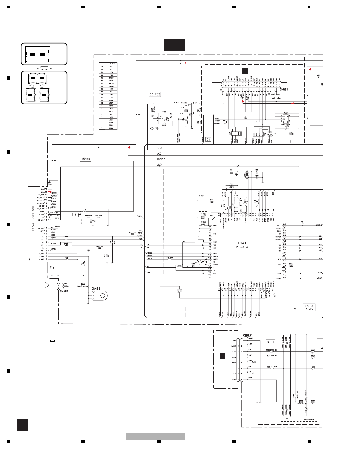
- Pin Functions(PE5449A)
1
4
7
8
9
10
11
12
13
14
15
16
17
18
21
22
23
24
25
26
27
28
29
30
31
32
33
34
35
36
37
38
39
40
41
42
43
46
47
48
49
50
51
52
53
54
55
56
57
58
59
60
61
Pin Name
MODEL1
NC
AVSS
NC
AVREF1
KYDT
DPDT
NC
TUNPDI
TUNPDO
TUNPCK
PCL
TESTIN
XSI
XSO
XSCK
NC
swvdd
ILMPW
NC
XRST
XA0
XSTB
CLAMSW
CONT
LOEJ
CLCONT
NC
DALMON
VSS1
BRST
BRXEN
BRSQ
ROMDATA
ROMCLK
ROMCS
RECIEVE
VDCONT
NC
SYSPW
NC
KEY2
NC
MUTE
ANTPW
NC
VST
VDT
VCK
NC
TUNPCE2
TUNPCE1
RDT
RDSLK
RDS57K
reset
LDET
Pin No.
2,3
5,6
19,20
44,45
Function and Operation
I/O
Model port 1
Not used
A/D GND
Not used
A/D converter reference voltage
Key data input
I
Display data output
O
Not used
PLL IC data input
I
PLL IC data output
O
PLL IC clock output
O
Clock adjustment output
O
Test program mode input
I
Serial data input
I
Serial data output
O
Serial data clock output
O
Not used
Keyboard unit power supply control output
O
Illumination power supply control output
O
Not used
CD LSI reset output
O
CD LSI identification control signal output
O
CD LSI strobe output
O
Not used
Servo driver power supply control output
O
CD load motor LOAD/EJECT direction exchange output
O
Driver input select output
O
Not used
Stand-by output
O
GND
Not used
Not used
Not used
ROM collection data output (Not used)
O
ROM collection clock output (Not used)
O
ROM collection chip select output (Not used)
O
During RDS data reception
VD control output
O
Not used
System power supply control output
O
Not used
Not used
Not used
System mute output
O
B. REMOTE output
O
Not used
Strobe pulse output for electronic volume
O
Data output for electronic volume
O
Clock output for electronic volume
O
Not used
EEPROM chip enable output 2
O
EEPROM chip enable output 1
O
RDS demodulation data input (Not used)
I
RDS LK signal input (Not used)
I
RDS 57kHz pulse count input (Not used)
I
Reset input
I
Not used
A
B
C
D
E
F
56
DEH-1750/XN/GS
7
8
49
Page 50

1234
Function and Operation
Pin No.
A
B
62
63
64
65
66
67
68
69
70
71
72
73
74
75
76
77
78
79
80
Pin Name
RCK
asens
bsens
DSENS
INTRQ
VSS0
VDD1
X2
X1
IC(VPP)
NC
XT1
VDD0
AVDD
SL
TEMP
VDSENS
DISCSENS
STRKEY1
I/O
RDS demodulation clock input (Not used)
I
ACC sense input
I
Back up sense input
I
Grille detach sense input
I
SOURCE key sense input
I
GND
Power supply
Crystal oscillator connection pin
Crystal oscillator connection pin
Connect to GND
Not used
Connect to GND
Power supply
Positive power supply terminal for analog circuit
SD level input from tuner
I
Connect to VDD
VD power supply voltage sense input
I
CD DISC sense input
I
NC
* PE5449A
80
1
C
20
21
D
BA33BC0FP
Vref
61
60
41
40
-
Vref
IC's marked by * are MOS type.
Be careful in handling them because they are very
liable to be damaged by electrostatic induction.
+
E
OCP TSD
1
2
NCOUT
F
50
1234
3
VCC
DEH-1750/XN/GS
Page 51

5678
49
48
33
32
17
16
1
64
- Pin Functions(PD6340A)
Pin No. Pin Name I/O Function and Operation
1-5 SEG4-0 O LCD segment output
6-9 COM3-0 O LCD common output
10 VLCD LCD drive power supply
11-14 KST3-0 O Key strobe output
15,16 KDT0,1 I Key data input (analogue input)
17 REW I Remote control reception input
18 DPDT I Display data input
19 NC Not used
20 KYDT O Key data output
21 MODA GND
22 X0 Crystal oscillator connection pin
23 X1 Crystal oscillator connection pin
24 VSS GND
25,26 KDT2,3 I Key data input
27 NC Not used
28 KST4 O Key strobe output
29-32 NC Not used
33-55 SEG35-13 O LCD segment output
56 VDD Power supply
57-64 SEG12-5 O LCD segment output
* PD6340A
A
B
C
D
E
56
DEH-1750/XN/GS
F
7
8
51
Page 52

1234
- Pin Functions(UPD63712AGC)
Pin No. Pin Name I/O Function and Operation
A
B
C
D
E
F
1 LD O Output of LD
2 PD I Input of PD
3 PN I Assignment of pickup polarity
4 AVDD Power supply for the analog system
5 DGND Ground for digital circuits
6 RFOK O Output of RFOK
7 INTQ O Interruption signals to the external microcomputer
8 rst I Input of reset
9 A0 I Command/Parameter discrimination signal input
10 stb I Data strobe signal input
11 sck I Serial data clock input
12 SO O Serial data output
13 SI I Serial data input
14 DVDD Power supply for digital circuits
15 DAVDD Power supply for DAC
16 ROUT O Output of audio for the right channel
17 DAGND GND for DAC
18 REGC Connected to the capacitor for band gap
19 DAGND GND for DAC
20 LOUT O Output of audio for the left channel
21 DAVDD Power supply for DAC
22 XVDD Power supply for the crystal oscillator
23 xtal O Connected to the crystal oscillator
24 XTAL I Connected to the crystal oscillator
25 XGND Ground for the crystal oscillator
26 DVDD Power supply for digital circuits
27 C1D1 O Information on error correction
28 C1D2 O Information on error correction
29 C2D1 O Information on error correction
30 C2D2 O Information on error correction
31 C2D3 O Information on error correction
32 LOCK O Output of LOCK
33 MIRR O MIRR signal
34 HOLD O HOLD signal
35 PLCK O Output of PLCK
36 C16M O Output of 16.9344MHz
37 DGND Ground for digital circuits
38 TX O DAI output
39 EMPH O Pre-emphasis information output
40 FLAG O The flag for which output sound data cannot be corrected is outputted
41 DVDD Power supply for digital circuits
42 LIMIT I Signal is inputted when the register can be read
43 xtalen I Permission to oscillate
44 DGND Ground for digital circuits
45 DIN I Input of audio data
46 DOUT O Output of audio data
47 SCKIN I Clock input for audio data
48 SCKO O Clock output for audio data
49 LRCKIN I Input of LRCK for audio data
50 LRCK O Output LRCK for audio data
51 DVDD Power supply for digital circuits
52 FD+ O Output of focus drive PWM
53 FD- O Output of focus drive PWM
54 TD+ O Output of tracking drive PWM
55 TD- O Output of tracking drive PWM
56 SD+ O Output of thread drive PWM
57 SD- O Output of thread drive PWM
58 MD+ O Output of spindle drive PWM
59 MD- O Output of spindle drive PWM
60 DGND Ground for digital circuits
52
1234
DEH-1750/XN/GS
Page 53

5678
Pin No. Pin Name I/O Function and Operation
61 TESTEN I Connected to GND
62-66 TEST4-0 I Connected to GND
67 ADGND GND for DAC
68 EFM O Output of EFM signals
69 ASY I Input of asymmetry
70 ADVDD Power supply for DAC
71 RFI I Input of RF
72, 73 EQ2, 1 Equalizer 2, 1
74 RF- I Reversal input of RF
75 RF2- I Reversal input of RF2
76 AGCO O Output of RF
77 AGCI I Input of AGC
78 RFO O Output of RF
79 ATEST O Analog tests
80 C3T Connection to the capacitor for detecting 3T
81 AGND Ground for the analog system
82 A I Input of A
83 C I Input of C
84 B I Input of B
85 D I Input of D
86 F I Input of F
87 E I Input of E
88 VREFIN I Photo-detector input bias voltage
89 AVDD Power supply for the analog system
90 REFOUT O Output of reference voltage
91 REFC Connected to the capacitor for output of REFOUT
92 FE- I Reversal input of FE
93 FEO O Output of FE
94 ADCIN I TEST
95 TE- I Reversal input of TE
96 TEO O Output of TE
97 TE2 O TE2
98 TEC I TEC
99 AGND Ground for the analog system
100 PWMSW I Servo PWM mode switching
A
B
C
* UPD63712AGC
50
51
75
76
D
26
25
E
1
100
F
56
DEH-1750/XN/GS
7
8
53
Page 54

1234
- Pin Functions(BA5835FP)
Pin No. Pin Name Function and Operation
A
B
C
1 VR Input pin for reference voltage
2 OPIN2(+) Input pin for non-inverting input for CH2 preamplifier
3 OPIN2(-) Input pin for inverting input for CH2 preamplifier
4 OPOUT2 Output pin for CH2 preamplifier
5 OPIN1(+) Input pin for non-inverting input for CH1 preamplifier
6 OPIN1(-) Input pin for inverting input from CH1 preamplifier
7 OPOUT1 Output pin for CH1 preamplifier
8 GND Ground pin
9 MUTE Mute control pin
10 POWVCC1 Power supply pin for CH1, CH2, and CH3 at "Power" stage
11 VO1(-) Driver CH1 - Negative output
12 VO1(+) Driver CH2 - Positive output
13 VO2(-) Driver CH2 - Negative output
14 VO2(+) Driver CH2 - Positive output
15 VO3(+) Driver CH2 - Positive output
16 VO3(-) Driver CH2 - Negative output
17 VO4(+) Driver CH4 - Positive output
18 VO4(-) Driver CH4 - Negative output
19 POWVCC2 Power supply pin for CH4 at "Power" stage
20 GND Ground pin
21 CNT Control pin
22 LDIN Loading input
23 OPOUTSL Output pin for preamplifier for thread
24 OPINLSL Input pin for preamplifier for thread
25 OPOUT3 CH3 preamplifier output pin
26 OPIN3(-) Input pin for inverting input for CH3 preamplifier
27 OPIN3(+) Input pin for non-inverting input for CH3 preamplifier
28 PREVCC PreVcc
BA5835FP
114
D
15 28
NJM2885DL1-33
Thermal
Protection
E
+
Bandgap
Reference
-
F
54
1234
DEH-1750/XN/GS
1
IN
2
GND
3
OUT
Page 55

5678
- FM/AM Tuner Unit
76 13 5 1098 11 14 18192021
NC
CE2
ROM_VDD
DI
SL
CK
NC
CE1
DO
NCNCNC
NC
A
VDD_3.3
3.3V
IC 5
←
5V 3.3V
IC 4
3.3V 2.5V
Rch
IC 2
2.5V
DET, FM MPX
←
2.5V
24
Lch
23
1
3
AM ANT
FM ANT
ATT
ATT
ANT adj
FMRF
FMRF
RF adj
IC 3 EEPROM
5.0V
OSC
LPF
IC 1
3.3V
MIXER, IF AMP
T51
CF52
RFGND
OSCGND
DGND
212 1522 16 4 17
AUDIOGNDNCVCC
No. Symbol I/O Explain
1 AMANT I AM antenna input AM antenna input high impedance AMANT pin is connected with
an all antenna by way of 4.7µH. (LAU type inductor) A series circuit
including an inductor and a resistor is connected with RF ground for
the countermeasure against the hum of power transmission line.
2 RFGND RF ground Ground of antenna block
3 FMANT I FM antenna input Input of FM antenna 75Ω Surge absorber(DSP-201M-S00B) is necessary.
4 VCC power supply The power supply for analog block. D.C 8.4V ± 0.3V
5 SL O signal level Output of FM/AM signals level
6 CE2 I chip enable-2 Chip enable for EEPROM ”Low” active
7 NC non connection Not used
8 CE1 I chip enable-1 Chip enable for AF•RF ”High” active
9 CK I clock Clock
10 DI I data in Data input
11 NC non connection Not used
12 OSCGND osc ground Ground of oscillator block
13 ROM_VDD power supply Power supply for EEPROM pin 13 is connected with a power supply of
micro computer.
14 DO O data out Data output
15 DGND digital ground Ground of digital block
16 NC non connection Not used
17 VDD_3.3 power supply The power supply for digital block. 3.3V ± 0.2V
18 NC non connection Not used
19 NC non connection Not used
20 NC non connection Not used
21 NC non connection Not used
22 AUDIOGND audio ground Ground of audio block
23 L ch O L channel output FM stereo “L-ch” signal output or AM audio output
24 R ch O R channel output FM stereo “R-ch” signal output or AM audio output
B
C
D
E
56
DEH-1750/XN/GS
F
7
8
55
Page 56

7.2.2 DISPLAY
- LCD(CAW1847)
A
B
1234
C
D
E
F
56
1234
DEH-1750/XN/GS
Page 57

5678
7.3 OPERATIONAL FLOW CHART
Power ON
VDD1=5V
Pin 68
bsens
Pin 64
bsens=L
asens
Pin 63
asens=L
DSENS
Pin 65
DSENS=L
A
B
C
Starts communication with Grille microcomputer.
300ms
swvdd←L
Pin 21
300ms
In case of the above signal, the communication
Source keys
operative
with Grille microcomputer may fail.
If the time interval is not 300msec, the oscillator
may be defective.
Source ON
SYSPW←H
Pin 43
Completes power-on operation.(After that, proceed to each source operation.)
D
E
56
DEH-1750/XN/GS
F
7
8
57
Page 58

1234
7.4 CLEANING
A
Before shipping out the product, be sure to clean the
following portions by using the prescribed cleaning
tools:
Portions to be cleaned Cleaning tools
CD pickup lenses Cleaning liquid : GEM1004
Cleaning paper : GED-008
B
C
D
E
F
58
1234
DEH-1750/XN/GS
Page 59

5678
8. OPERATIONS
A
B
C
D
E
56
DEH-1750/XN/GS
F
7
8
59
Page 60

1234
A
B
C
D
E
F
60
1234
DEH-1750/XN/GS
Page 61

5678
- CONNECTION DIAGRAM
Power amp
separately)
(sold
A
.
Right
Connecting cords with RCA
pin plugs (sold separately)
Fuse
System remote control
Blue/white
Tosystem controlterminal ofthe power amp or
Auto-antenna relay control terminal (max. 300 mA
12 V DC).
Rear speaker
Perform these connections whenusing
+
≠
+
≠
Rear speaker
the optional amplifier
+
Gray
White
+
Front speaker
≠
≠
Front speaker
+
Violet
Gray/black
Green
White/black
+
Left
Rear speaker
≠
≠
rRea speaker
Violet/black
Green/black
With a 2 speaker system, do not
connect anything to the speaker leads
that are not connectedto speakers.
B
C
D
This Product
Antenna jack
Rear output
Yellow
DEH-1750/XN/GS
56
Toterminal alwayssupplied with
7
power regardless of ignition
switch position.
Red
E
Toelectric terminalcontrolled by
ignition switch (12 V DC)
ON/OFF.
Black (ground)
Tovehicle (metal)body.
F
8
61
Page 62

1234
sc
82
g
ggg
g
ggg
)
e
.
s
Jigs List
Nam
Test Di
A
B
Jig No
TCD-7
Remark
Checking the gratin
Checking the gratin
Two pieces
C
D
E
F
62
1234
DEH-1750/XN/GS
 Loading...