

Pioneer CX-958 Service manual

Model No. Order No. CD Mechanism Module Mechanism Unit
DEH-P410/X1N/UC CRT2414 CXK5201 CXB4800
DEH-P4100/X1N/UC
DEH-P310/X1N/UC
DEH-P41/X1N/UC CRT2415 CXK5201 CXB4800
DEH-P3100/X1N/UC
DEH-P4150/X1N/ES CRT2416 CXK5201 CXB4800
DEH-P3150/X1N/ES
DEH-P4100R/X1N/EW CRT2417 CXK5201 CXB4800
DEH-3110/X1N/EE
DEH-3130R/X1N/EW CRT2418 CXK5201 CXB4800
DEH-3100R-B/X1N/EW
DEH-3100R/X1N/EW
PIONEER CORPORATION 4-1, Meguro 1-Chome, Meguro-ku, Tokyo 153-8654, Japan
PIONEER ELECTRONICS SERVICE INC. P.O.Box 1760, Long Beach, CA 90801-1760 U.S.A.
PIONEER ELECTRONIC [EUROPE] N.V. Haven 1087 Keetberglaan 1, 9120 Melsele, Belgium
PIONEER ELECTRONICS ASIACENTRE PTE.LTD. 253 Alexandra Road, #04-01, Singapore 159936
C PIONEER CORPORATION 1999
K-ZZA. OCT. 1999 Printed in Japan
ORDER NO.
CRT2423
CD MECHANISM MODULE
CX-958
- This service manual describes the operation of the CD mechanism incorporated in models listed in the
table below.
- When performing repairs use this manual together with the specific manual for model under repair.
CONTENTS
1. CIRCUIT DESCRIPTIONS ...........................................2
2. MECHANISM DESCRIPTIONS.................................17
3. DISASSEMBLY .........................................................18
2
CX-958
1. CIRCUIT DESCRIPTIONS
The LSI (UPD63711GC) used on this unit comprises six main blocks ; the pre-amp section, servo, signal processor,
DAC, CD text decoder (not used on this model) and LPF. It also equips with nine automatic adjustment functions.
1.1 PRE-AMP SECTION
This section processes the pickup output signals to
create the signals for the servo, demodulator and
control.
The pickup output signals are I-V converted by the preamp with the built-in photo-detector in the pickup, then
added by the RF amp to obtain RF, FE, TE, TE zero cross
and other signals.
This pre-amp section is built in the servo LSI
UPD63711GC (IC201). The following describes function
of each section.
Since this system has a single power supply (+5V), the
reference voltage for this LSI and pickup are set to
REFO (2.5V). The REFO is obtained by passing the
REFOUT from the LSI through the buffer amplifier. The
REFO is output from Pin 89 of this LSI. All
measurements are done using this REFO as reference.
Note : During the measurement, do not try to short the
REFO and GND.
1) APC Circuit (Automatic Power Control)
When the laser diode is driven with constant current,
the optical output has large negative temperature
characteristics. Thus, the current must be controlled
from the monitor diode so that the output may be
constant. APC circuit is for it. The LD current is obtained
by measuring the voltage between LD1 and V+5. The
value of this current is about 35mA.
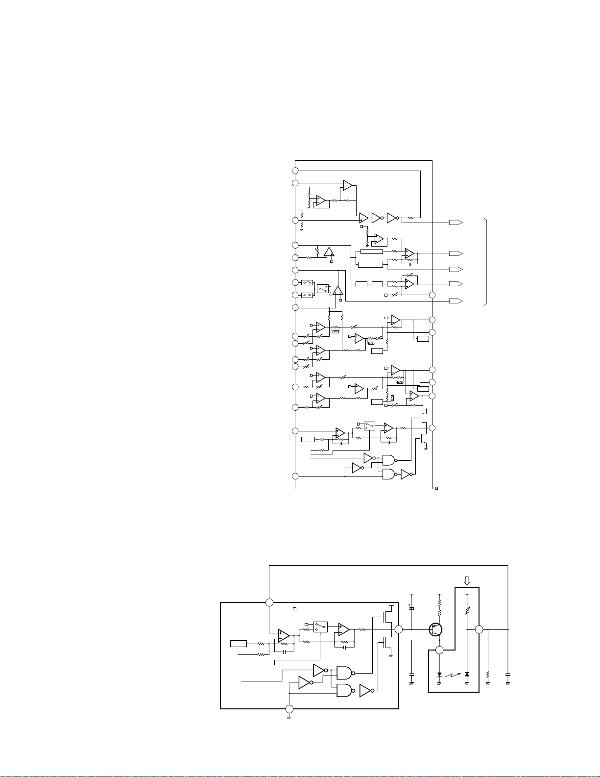
Fig.1 : BLOCK DIAGRAM OF BUILT-IN RF AMPLIFIER
Fig.2 : APC CIRCUIT
EFM
ASY
AGCO
AGCI
RFO
EQ2
EQ1
71
72
RFI
74
75
76
77
78
79
RF-
80
Vref
A
82
C
83
Vref
B
84
D
85
Vref
F
86
Vref
E
87
PD
97
VREG
GND
APN
LDON
Vref
PEAK DET.
Vref
Vref
BOTTOM DET.
LPF
S/H
Vref
Vref
Vref
Vref
Vref
D/A
Vref
D/A
Vref
Vref
73
91
90
A/D
93
92
A/D
94
98
C-3T
FEO
FE-
TEO
TE-
TE2
LD
EFM
MIRR
DEFECT
A3T
FOK
To the
following stage
of the LSI
PD
16k
VREG
GND
AMP_PN
(H:Nch L:Pch)
LDON
(H:LD MOVE L:STOP)
1k
PN
99
·····Vref(+2.5V)
+5V
C103
97
150k
3p
·····Vref(+2.5V)
Vref
99
PN
100k
100k
110k
1k
3p
LD
98
100µF/6.3V
Q101
2SB1132
C102
0.1µF
R102
10
R101
12
14
PU UNIT
5
R103
C105
2.2k
0.33µF
CX-958
3
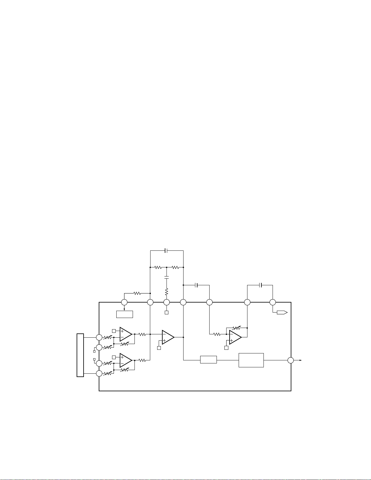
2) RF Amplifier and RFAGC Amplifier
The photo-detector outputs (A +C) and (B +D) are
added, amplified and equalized on this LSI and then
output to the RFI terminal as the RF signal. (The eye
pattern can be checked by this signal.)
The RFI voltage low frequency component is :
RFI = (A +B +C +D) ×3.2
RFI is used on the FOK generator circuit and RF offset
adjusting circuit.
R207 is an offset resistor for maintaining the bottom
reference voltage of the RFI signal at 1.5 VDC. The D/A
output used for the RF offset adjustment (to be
described later) is entered via this resistor.
After the RFI signal from Pin 77 is externally AC
coupled, entered to Pin 76 again, then amplified on the
RFAGC amplifier to obtain the RFO signal.
The RFAGC adjustment function (to be described later)
built-in the LSI is used for switching feedback gain of
the RFAGC amplifier so that the RFO output may go to
1.5 ±0.3Vpp.
The RFO signal is used for the EFM, DFCT, MIRR and
RFAGC adjustment circuits.
3) RFOK Circuit
This circuit generates the signal that is used for
indicating the timing of closing the focus or state of the
focus close currently being played. This signal is output
from Pin 4 as the FOK signal. It goes high when the
focus close and in-play.
The RFOK signal is generated by holding DC level of the
RFI at its peak with the succeeding digital section, then
comparing it at a specific threshold level. Thus, the
RFOK signal goes high even if the pit is absent. It
indicates that the focus close can take place on the disc
mirror surface, too.
This signal is also supplied to the micro computer via
the low pass filter as the FOK signal and used for the
protection and the RF amplifier gain switching.
Fig.3 : RFAMP, RFAGC AND FOK CIRCUIT
CN101
6
13
A+C
B+D
C216 3pF
R205
10k
C217
27pF
R207
12k
66
D/A
10k
82
83
84
85
10k
16k
16k
R206
1.8k
80 79 74757677
10k
10k
R204
10k
C215
0.1µF
A/D
10k
12k
3900pF
RFOAGCIRFI
FOK
CIRCUIT
C213
TO EFM
CIRCUIT
FOK
4
4
CX-958
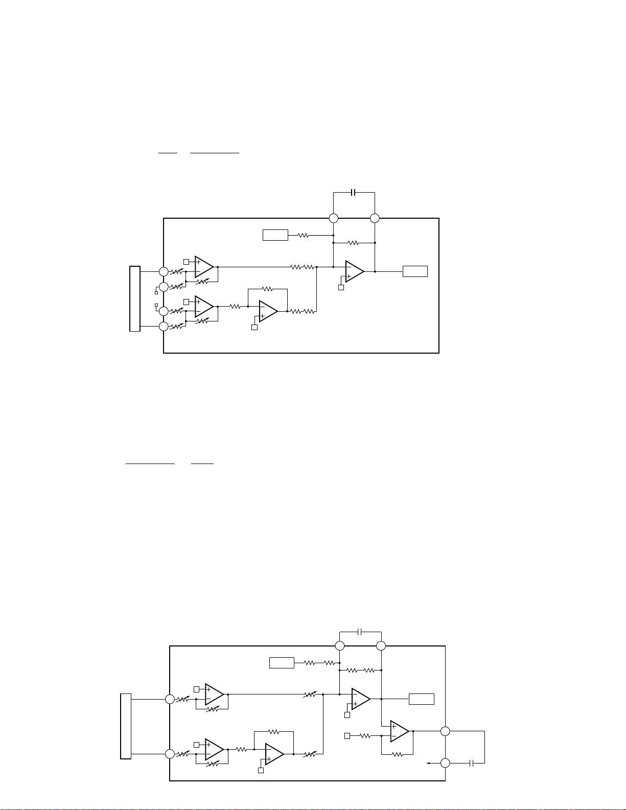
Fig.5 TRACKING ERROR AMPLIFIER AND TRACKING ZERO CROSSING AMPLIFIER
4) Focus Error Amplifier
The photo-detector outputs (A+C) and (B+D) are passed
through a differential amplifier and an error amplifier, and
then (A+C−B−D) is output from Pin 91 as the FE signal.
The FE voltage low frequency component is :
FE = (A + C − B − D) ××
= (A + C − B − D) × 5
Using REFO as the reference, an S-curve of approximately 1.5
Vpp is obtained for the FE output. The final-stage amplifier
cutoff frequency is 11.4 kHz.
5) Tracking Error Amplifier
The photo-detector outputs E and F are passed through
a differential amplifier and an error amplifier, and then
(E −F) is output from Pin 93 as the TE signal. The TE
voltage low frequency component is :
TE =(E −F)
××
=
(E −F) ×6.6 (Effective LSI output is 5.0).
Using REFO as the reference, the TE waveform of
approximately 1.3 Vpp is obtained for the TE output.
The final-stage amplifier cutoff frequency is 20 kHz.
6) Tracking Zero Crossing Amplifier
TEC signal (the tracking zero crossing signal) is
obtained by multiplying the TE signal four times. It is
used for locating the zero crossing points of the
tracking error. The zero cross point detection is done for
the following two reasons :
1
To count tracks for carriage moves and track jumps.
2
To detect the direction in which the lens is moving
when the tracking is closed (it is used on the
tracking brake circuit to be described later).
The TEC signal frequency range is 300 Hz to 20 kHz.
TEC voltage =TE level ×4
Theoretical TEC level is 5.2V. The signal exceeds Drange of the operational amplifier and thus is clipped.
It, however, can be ignored since this signal is used by
the servo LSI only at the zero crossing point.
20k5k
CN101
84
6
13
83
82
10k
20k
5k
85
A+C
16k
B+D
48k
16k
10k
9190
D/A
80k
110k
FE
C219 180pF
A/D
FE OFFSET
TO DIG. EQ
48k
48.7k
CN101
9
11
86
112k
48.7k
87
F
E
F
224k
E
48k
224k
112k
9392
D/A
80k
110k
TE
C220 51pF
80k
110k
A/D
TE OFFSET
TO DIG. EQ
48k
60k
20k
95
94
TE2
TEC
C221
6800pF
16k
10k
80k
(20k + 5k)
Fig.4 : FOCUS ERROR AMPLIFIER
224k
112k
160k
48.7k
CX-958
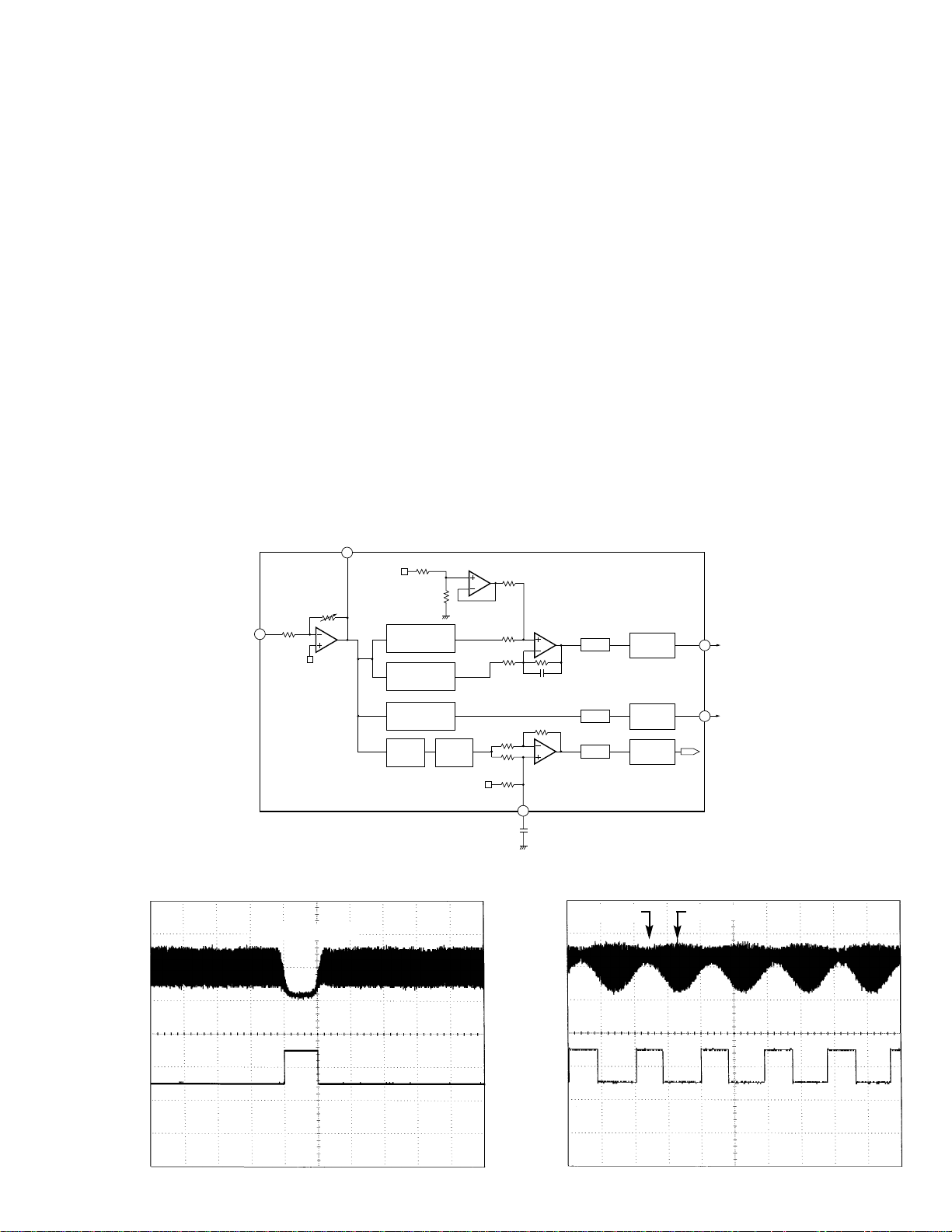
7) DFCT (Defect) Circuit
The DFCT signal is used for detecting defects on the
mirrored disc surface. It allows monitoring from the
HOLD pin (Pin 2). It goes high when defects are found
on the mirrored surface.
The DFCT signal is generated by comparing the RF
amplified signal (which is obtained by bottom holding
the RFO signal) at a specific threshold level by the
succeeding digital section.
Stains or scratches on the disc can constitute the
defects on the mirrored disc surface. Thus, as long as
the DFCT signal remains high in the LSI, the focus and
tracking servo drives are held in the current state so
that a better defect prevention may be ensured.
8) 3TOUT Circuit
The 3TOUT signal is generated by entering disturbance
to the focus servo loop, comparing phase of
fluctuations of the RF signal 3T component against that
of the FE signal at that time, then converting the signal
to DC level. This signal is used for adjusting bias of the
FE signal (to be described later). This signal is not
output from the LSI, thus its monitoring is not available.
9) MIRR (Mirror) Circuit
The MIRR signal shows the on track and off track data,
and is output from Pin 3.
When the laser beam is
On track : MIRR ="L"
Off track : MIRR ="H"
This signal is used on the brake circuit (to be described
later) and also as the trigger to turn on track counting
when jumping take place.
The MIRR signal is supplied to the micro computer, too,
for the protection purpose.
A/D
MIRR
CIRCUIT
3T
CIRCUIT
DFCT
CIRCUIT
BOTTOM DETECT
BOTTOM DETECT
PEAK DETECT
LPFS/H
A/D
A/D
76
75
73
3
2
40k
20k
20k
40k
40k
40k
200k
200k
C212
0.1µF
C3T
AGCI
RFO
12k
10k
20k
30k
MIRR
HOLD
Fig.6 : DFCT, MIRR AND 3T DETECTION CIRCUIT
Fig.7 : HOLD OUTPUT WAVEFORM
(When surface defects are present)
Fig.8 : MIRR OUTPUT WAVEFORM
(When an access is made)
5
Surface defects
RFI
HOLD
RFI
MIRR
OFF Track ON Track
6
CX-958
10) EFM Circuit
This circuit is used for converting the RF signal to
digital signal consisting of “0” and “1”. The RFO signal
from Pin 75 is externally AC coupled, entered to Pin 74,
then applied to the EFM circuit.
Loss of the RF signal due to scratches or stains on the
disc, or vertical asymmetry of the RF due to variations
in the discs manufactured can’t be eliminated by AC
coupling alone. This circuit, therefore, controls the
reference voltage ASY on the EFM comparator by use
of the fact that “0” and “1” appear fifty fifty in the EFM
signal. By this arrangement, the comparate level is
constantly maintained at almost center of the RFO
signal level. The reference voltage ASY is generated
when the EFM comparator output is passed through
the low pass filter. The EFM signal is output from Pin
71. It is a 2.5 Vp-p amplitude signal centering on REFO.
Fig.9 : EFM CIRCUIT
C213
3900pF
RFI
EFM. SIG
40k
74
40k
15k75k
2k
71
72
40k
40k
EFM
ASY
C211
0.1µF
R202
10k
R203
39k
C210
3300pF
 Loading...