

Page 1

Model Service Manual CD Mechanism Module Mechanism Unit
CDX-P1250/X1N/UC,ES CRT2318 CXK4900 CXB3008
CDX-P1250/X1N/EW CXK4905 CXB3008
CDX-FM1259/X1N/UC CRT2320 CXK4916 CXB3008
CDX-FM1257/X1N/UC,ES CXK4915 CXB3008
PIONEER ELECTRONIC CORPORATION 4-1, Meguro 1-Chome, Meguro-ku, Tokyo 153-8654, Japan
PIONEER ELECTRONICS SERVICE INC. P.O.Box 1760, Long Beach, CA 90801-1760 U.S.A.
PIONEER ELECTRONIC [EUROPE] N.V. Haven 1087 Keetberglaan 1, 9120 Melsele, Belgium
PIONEER ELECTRONICS ASIACENTRE PTE.LTD. 253 Alexandra Road, #04-01, Singapore 159936
C PIONEER ELECTRONIC CORPORATION 1999
K-ZZU. FEB. 1999 Printed in Japan
ORDER NO.
CRT2357
CD MECHANISM MODULE
CX-938
- This service manual describes the operation of the CD mechanism incorporated in models listed in the
table below.
- When performing repairs use this manual together with the specific manual for model under repair.
CONTENTS
1. CIRCUIT DESCRIPTIONS...........................................2
2. DISASSEMBLY .........................................................18
3. MECHANISM DESCRIPTIONS.................................23
Page 2
2
C X-938
1. CIRCUIT DESCRIPTIONS
The LSI (UPD63710GC) used on this unit comprises five main blocks ; the pre-amp section, servo, signal processor,
DAC and CD text decoder (not used on this model). It also equips with nine automatic adjustment functions.
1.1 PRE-AMP SECTION
This section processes the pickup output signals to
create the signals for the servo, demodulator and
control.
The pickup output signals are I-V converted by the preamp with the built-in photo-detector in the pickup, then
added by the RF amp to obtain RF, FE, TE, TE zero cross
and other signals.
This pre-amp section is built in the servo LSI
UPD63710GC (IC201). The following describes function
of each section.
Since this system has a single power supply (+5V), the
reference voltage for this LSI and pickup are set to
REFO (2.5V). The REFO is obtained by passing the
REFOUT from the LSI through the buffer amplifier. The
REFO is output from Pin 89 of this LSI. All
measurements are done using this REFO as reference.
Note : During the measurement, do not try to short the
REFO and GND.
1) APC Circuit (Automatic Power Control)
When the laser diode is driven with constant current,
the optical output has large negative temperature
characteristics. Thus, the current must be controlled
from the monitor diode so that the output may be
constant. APC circuit is for it. The LD current is obtained
by measuring the voltage between LD1 and V+5. The
value of this current is about 35mA.
71
72
74
76
AGCI
77
RFO
75
78
79
80
73
91
90
93
92
C-3T
FEO
FE-
TEO
TE-
85
86
87
E
97
PD
99
PN
F
D
82
83
84
B
C
A
RF-
EQ1
EQ2
AGCO
RFI
ASY
EFM
PEAK DET.
LPF
BOTTOM DET.
S/H
D/A
A/D
D/A
A/D
94
98
TE2
LD
VREG
GND
APN
LDON
EFM
DEFECT
FOK
A3T
MIRR
To the
following stage
of the LSI
Vref
Vref
Vref
Vref
Vref
Vref
Vref
Vref
Vref
Vref
Vref
Vref
Vref
Vref
Vref
·····Vref(+2.5V)
97
PD
99
PN
98
LD
VREG
GND
AMP_PN
(H:Nch L:Pch)
LDON
(H:LD MOVE L:STOP)
Vref
·····Vref(+2.5V)
14
5
R102
10
R101
12
Q101
2SB1132
C102
0.1µF
C103
100µF/6.3V
PU UNIT
R103
2.2k
C105
0.33µF
+5V
1k
110k
3pF
3pF
150k
100k
100k
16k
1k
Fig.1 : BLOCK DIAGRAM OF BUILT-IN RF AMPLIFIER
Fig.2 : APC CIRCUIT
Page 3
C X-938
3
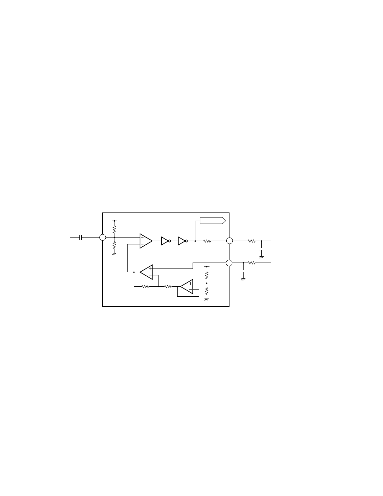
2) RF Amplifier and RFAGC Amplifier
The photo-detector outputs (A +C) and (B +D) are
added, amplified and equalized on this LSI and then
output to the RFI terminal as the RF signal. (The eye
pattern can be checked by this signal.)
The RFI voltage low frequency component is :
RFI = (A
+B +C +
D) ×3.2
RFI is used on the FOK generator circuit and RF offset
adjusting circuit.
R215 is an offset resistor for maintaining the bottom
reference voltage of the RFI signal at 1.5 VDC. The D/A
output used for the RF offset adjustment (to be
described later) is entered via this resistor.
After the RFI signal from Pin 77 is externally AC
coupled, entered to Pin 76 again, then amplified on the
RFAGC amplifier to obtain the RFO signal.
The RFAGC adjustment function (to be described later)
built-in the LSI is used for switching feedback gain of
the RFAGC amplifier so that the RFO output may go to
1.5
±
0.3Vpp.
The RFO signal is used for the EFM, DFCT, MIRR and
RFAGC adjustment circuits.
3) FOK Circuit
This circuit generates the signal that is used for
indicating the timing of closing the focus or state of the
focus close currently being played. This signal is output
from Pin 4 as the FOK signal. It goes high when the
focus close and in-play.
The RFOK signal is generated by holding DC level of the
RFI at its peak with the succeeding digital section, then
comparing it at a specific threshold level. Thus, the
RFOK signal goes high even if the pit is absent. It
indicates that the focus close can take place on the disc
mirror surface, too.
This signal is also supplied to the micro computer via
the low pass filter as the FOK signal and used for the
protection and the RF amplifier gain switching.
CN101
84
18
25
83
82
10k
10k
85
FOK
CIRCUIT
A/D
4
A+C
16k
B+D
10k
16k
10k
R215
12k
C209 3pF
R214
10k
R207
1.8k
C208
27pF
R213
10k
80 79 74757677
D/A
12k
66
10k
RFOAGCIRFI
C207
0.22µF
C206
3900pF
FOK
TO EFM
CIRCUIT
Fig.3 : RFAMP, RFAGC AND FOK CIRCUIT
Page 4
5) Tracking Error Amplifier
The photo-detector outputs E and F are passed through
a differential amplifier and an error amplifier, and then
(E −F) is output from Pin 93 as the TE signal. The TE
voltage low frequency component is :
TE
=
(E −F)
××
=
(E −F) ×5.7 (Effective LSI output is 5.0).
Using REFO as the reference, the TE waveform of
approximately 1.3 Vpp is obtained for the TE output.
The final-stage amplifier cutoff frequency is 20 kHz.
6) Tracking Zero Crossing Amplifier
TEC signal (the tracking zero crossing signal) is
obtained by multiplying the TE signal four times. It is
used for locating the zero crossing points of the
tracking error. The zero cross point detection is done for
the following two reasons :
1
To count tracks for carriage moves and track jumps.
2
To detect the direction in which the lens is moving
when the tracking is closed (it is used on the
tracking brake circuit to be described later).
The TEC signal frequency range is 300 Hz to 20 kHz.
TEC voltage
=
TE level ×4
Theoretical TEC level is 5.2V. The signal exceeds Drange of the operational amplifier and thus is clipped.
It, however, can be ignored since this signal is used by
the servo LSI only at the zero crossing point.
4
C X-938
Fig.5 TRACKING ERROR AMPLIFIER AND TRACKING ZERO CROSSING AMPLIFIER
4) Focus Error Amplifier
The photo-detector outputs (A+C) and (B+D) are passed
through a differential amplifier and an error amplifier, and
then (A
+C−B−
D) is output from Pin 91 as the FE signal.
The FE voltage low frequency component is :
FE
= (A + C − B − D) ××
=
(A + C − B − D) × 5
Using REFO as the reference, an S-curve of approximately 1.5
Vpp is obtained for the FE output. The final-stage amplifier
cutoff frequency is 11.4 kHz.
20k
CN101
84
18
25
83
82
10k
20k
85
A+C
16k
B+D
48k
16k
10k
9190
D/A
80k
110k
FE
C210 220pF
R208 300k
A/D
FE OFFSET
TO DIG. EQ
48k
38k
CN101
21
23
86
56k
38k
87
F
E
F
224k
E
48k
224k
56k
9392
D/A
80k
110k
TE
C211 100pF
A/D
TE OFFSET
TO DIG. EQ
48k
R216
27k
R215
27k
60k
20k
95
94
TE2
TEC
R212
0
C212
6800pF
16k
10k
(80k//300k)
20k
Fig.4 : FOCUS ERROR AMPLIFIER
224k
(56k
+27k)
80k
38k
Page 5
C X-938
7) DFCT (Defect) Circuit
The DFCT signal is used for detecting defects on the
mirrored disc surface. It allows monitoring from the
HOLD pin (Pin 2). It goes high when defects are found
on the mirrored surface.
The DFCT signal is generated by comparing the RF
amplified signal (which is obtained by bottom holding
the RFO signal) at a specific threshold level by the
succeeding digital section.
Stains or scratches on the disc can constitute the
defects on the mirrored disc surface. Thus, as long as
the DFCT signal remains high in the LSI, the focus and
tracking servo drives are held in the current state so
that a better defect prevention may be ensured.
8) 3TOUT Circuit
The 3TOUT signal is generated by entering disturbance
to the focus servo loop, comparing phase of
fluctuations of the RF signal 3T component against that
of the FE signal at that time, then converting the signal
to DC level. This signal is used for adjusting bias of the
FE signal (to be described later). This signal is not
output from the LSI, thus its monitoring is not available.
9) MIRR (Mirror) Circuit
The MIRR signal shows the on track and off track data,
and is output from Pin 3.
When the laser beam is
On track : MIRR ="L"
Off track : MIRR
=
"H"
This signal is used on the brake circuit (to be described
later) and also as the trigger to turn on track counting
when jumping take place.
The MIRR signal is supplied to the micro computer, too,
for the protection purpose.
A/D
MIRR
CIRCUIT
3T
CIRCUIT
DFCT
CIRCUIT
BOTTOM DETECT
BOTTOM DETECT
PEAK DETECT
LPFS/H
A/D
A/D
76
75
73
3
2
40k
20k
20k
40k
40k
40k
200k
200k
C205
0.1µF
C3T
AGCI
RFO
12k
10k
20k
30k
MIRR
HOLD
Fig.6 : DFCT, MIRR AND 3T DETECTION CIRCUIT
Fig.7 : HOLD OUTPUT WAVEFORM
(When surface defects are present)
Fig.8 : MIRR OUTPUT WAVEFORM
(When an access is made)
5
Surface defects
RFI
HOLD
RFI
MIRR
OFF Track ON Track
Page 6
6
C X-938
10) EFM Circuit
This circuit is used for converting the RF signal to
digital signal consisting of “0” and “1”. The RFO signal
from Pin 75 is externally AC coupled, entered to Pin 74,
then applied to the EFM circuit.
Loss of the RF signal due to scratches or stains on the
disc, or vertical asymmetry of the RF due to variations
in the discs manufactured can’t be eliminated by AC
coupling alone. This circuit, therefore, controls the
reference voltage ASY on the EFM comparator by use
of the fact that “0” and “1” appear fifty fifty in the EFM
signal. By this arrangement, the comparate level is
constantly maintained at almost center of the RFO
signal level. The reference voltage ASY is generated
when the EFM comparator output is passed through
the low pass filter. The EFM signal is output from Pin
71. It is a 2.5 Vp-p amplitude signal centering on REFO.
74
RFI
40k
40k
C206
3900pF
72
71
ASY
EFM
40k
40k
15k75k
2k
R205
10k
R206
39k
C203
0.1µF
C204
3300pF
EFM. SIG
Fig.9 : EFM CIRCUIT
Page 7
7
C X-938
1.2 SERVO SECTION (UPD63710GC :
IC201)
The servo section controls the operations such as error
signal equalizing, in focus, track jump and carriage
move. The DSP is the signal processing section used
for data decoding, error correction and interpolation
processing, among others.
This circuit implements analog to digital conversion of
the FE and TE signals generated on the pre-amplifier,
then outputs them through the servo block as the drive
signal used on the focus, tracking and carriage system.
The EFM signal is decoded on the signal processing
section and finally output via the D/A converter as the
audio signal. The decoding process also generates the
spindle servo error signals which is fed to the spindle
servo block to generate the spindle drive signal.
The focus, tracking, carriage and spindle drive signals
are then amplified on the driver IC BA5986FM (IC301)
and fed to respective actuators and motors.
1) Focus Servo System
The focus servo main equalizer is consisted of the
digital equalizer. Fig.10 shows the focus servo block
diagram.
When implementing the focus close on the focus servo
system, the lens must be brought within the in-focus
range. Therefore, the lens is moved up and down
according to the triangular focus search voltage to find
the focus point. During this time, the spindle motor is
kicked and kept rotating as a set speed.
The servo LSI monitors the FE and RFOK signals and
automatically carries out the focus close at an
appropriate point.
The focus closing is carried out when the following
three conditions are met :
1
The lens approaches the disc from its current
position.
2
RFOK
=
"H"
3
The FZC signal is latched at high after it has once
crossed the threshold set on the FZD register (Edge
of the FZD).
As the result, the FE (
=
REFO) is forced to low.
FE
AMP
DIG.
EQ
82
A+C
B+D
FD
FOP
FOM
IC301
BA5986FM
LENS
IC201 UPD63710GC
85
62
3
4
14
13
FOCUS SEARCH
TRIANGULAR
WAVE GENERATOR
DAC
CONTROL
A/D
R302
15k
R301
10k
Fig.10 : FOCUS SERVO BLOCK DIAGRAM
Page 8
8
C X-938
When the above conditions are all met and the focus is
closed, the XSI pin goes to low from the current high,
then 40 ms later, the microcomputer begins to monitor
the RFOK signal after it that has been passed through
the low pass filter.
When the RFOK signal is recognized as low, the micro
computer carries out various actions including
protection.
Fig.11 a series of operations carried out relevant to the
focus close (the figure shows the case where focus
close is not available).
You can check the S-curve, search voltage and actual
lens behavior by selecting the Display 01 for the focus
mode select in the test mode, and then pressing the
focus close button.
REFO
FD
LENS POSITION
RELATIVE TO DISC
NEAR
FAR
"JUST FOCUSED"
MD
REFO
Expanding around "Just Focused Point"
REFO
RFI
FOK
FE
FZD
THRESHOLD
LEVEL
FZD
(INTERNAL SIGNAL)
Focus closing would normally take place at these points
XSI
(IN THE EVENT
FOCUS IS
CLOSED)
LEVEL
Fig.11 : FOCUS CLOSE SEQUENCE
Page 9
9
C X-938
2) Tracking Servo System
The digital equalizer is employed for the main equalizer
on the tracking servo. Fig.12 shows the tracking servo
block diagram.
a) Track jump
When the LSI receives the track jump command from
the microcomputer, the operation is carried out
automatically by the auto sequence function of the LSI.
This system has five types of track jumps used for the
search : 1, 4, 10, 32 and 32 ×3. In the test mode, in
addition to three jumps (1, 32 and 32
×
3), move of the
carriage can be check by mode selection. For track
jumps, the microcomputer sets almost half of tracks (5
tracks for 10 tracks, for instance) and counts the set
number of tracks using the TEC signals. When the
microcomputer has counted the set number of tracks, it
outputs the brake pulse for a fixed period of time
(duration can be specified with the command) to stop
the lens. In this way, the tracking is closed and normal
play is continued.
To improve the servo loop retracting performance just
after the track jump, the brake circuit is turned on for 50
ms after the brake pulse has been terminated to
increase gain of the tracking servo.
Fast forward and reverse operations are realized by
through consecutive signal track jumps. The speed is
about 10 times as fast as that in the normal mode.
TOP
TOM
IC301
BA5986FM
LENS
11
12
6
7
R304
15k
R303
10k
TE
AMP
DIG.
EQ
86
F
E
TD
IC201 UPD63710GC
87
63
JUMP
PARAMETERS
DAC
CONTROL
A/D
t1
t2
GAIN NORMAL
TD
KICK
BRAKE
TEC
T. BRAKE
EQUALIZER
T. SERVO
CLOSED
OPEN
NORMAL
GAIN UP
OFF
ON
t1
TD
TEC
(10 TRACK)
EQUALIZER
T. BRAKE
SERVO
SD
2.9mS (4.10 TRACK JUMP)
5.8mS (32 TRACK JUMP)
GAIN UP
NORMAL
ON
OFF
OPEN
CLOSED
t2
50mS
t
Fig.12 : TRACKING SERVOBLOCK DIAGRAM
Fig.13 : SINGLE TRACK JUMP
Fig.14 : MULTI-TRACK JUMP
Page 10

10
C X-938
b) Brake Circuit
The servo retracting performance can be deteriorate
during the setup or track jump operation. In this
connection, the brake circuit is used to ensure steady
retract of the tracking servo. The brake circuit detects in
which direction the lens is moving, then slows down its
move by outputting the drive signal that moves the
lens into the opposite direction alone. Track slippage
direction is determined by referencing the TEC and
MIRR signals and their phase.
TEC
TZC
(TEC "SQUARED UP" )
(INTERNAL SIGNAL )
MIRR
MIRR LATCHED AT
TZC EDGES
=
SWITCHING PULSE
EQUALIZER OUTPUT
(SWITCHED)
DRIVE DIRECTION
Note : Equalizer output assumed to hava same phase as TEC.
FORWARD
LENS MOVING FORWARDS
(INNER TRACK TO OUTER)
LENS MOVING BACKWARDS
Time
REVERSE
Fig.15 : TRACKING BRAKE CIRCUIT
Page 11

11
C X-938
3) Carriage Servo System
The carriage servo supplies the tracking equalizer’s
low-frequency component (lens position data) output to
the carriage equalizer, then, after providing a fixed
amount of gain to it, outputs the drive signal from the
LSI. This signal is then applied to the carriage motor via
the driver IC.
When the lens offset reaches a certain level during play,
the entire pickup must be moved into the forward
direction. Therefore, the equalizer gain is set to the
level that allows to generate a voltage higher than the
carriage motor starting voltage. In actual operations, a
certain threshold level is set for the equalizer output by
the servo LSI so that the drive voltage may be output
from the servo LSI only when the equalizer output
exceeds the threshold level. This arrangement helps
reducing power consumption. Also, due to disc
eccentricity or other factors, the equalizer output may
cross the threshold level a number of times. In this
case, the drive voltage output from the LSI will have
pulse-like waveform.
COP
COM
IC301
BA5986FM
CARRIAGE
MOTOR
15
16
M
DIG.
EQ
SD
IC201 UPD63710GC
64
KICK, BRAKE
REGISTERS
DAC
CONTROL
FROM
TRACK. EQ
26
25
R306
7.5k
R305
10k
DRIVE ON/OFF THRESHOLD
CARRIAGE MOVED AT THESE POINTS
TRACKING DRIVE
(LOW FREQUENCY)
LENS POSITION
CRG DRIVE
(INSIDE UPD63710GC)
CRG MOTOR VOLTAGE
Fig.16 : CARRIAGE SERVOBLOCK DIAGRAM
Fig.17 : CARRIAGE SIGNAL WAVEFORM
Page 12

12
C X-938
4) Spindle Servo System
The spindle servo has the following modes.
1
Kick :
This mode is used for accelerating the disc rotation
during setup.
2
Offset :
(a) After the kick is over in the setup, this mode is
turned on until changing to rough servo mode.
(b) When focus is lost during play, this mode is
turned on until the focus is restored.
Both of the above are used for maintaining the disc
rotation rate near to the specified rate.
3
Applicable servo :
The CLV servo mode is turned on for the normal
operations.
In the EFM demodulation block, the frame sync
signal and internal counter output signal are
sampled for every WFCK/16 and a signal is produced
for indicating whether or not they are matching.
They are determined to be asynchronous only when
this signal fails to match 8 times in succession. In all
other cases, above two signals are assumed to be
synchronous. In the applicable servo mode, the
retracting servo is automatically selected if the two
signals are synchronous. If not, the regular servo is
automatically selected.
4
Brake :
This mode is turned on when stopping the spindle
motor.
The microcomputer outputs the brake voltage
through the servo LSI. The LSI monitors the EFM
waveform and, if its longest pattern exceeds a
certain interval (if the rotation is sufficiently slow),
the flag is set the LSI and the microcomputer turns
off the brake voltage. When the flag is not up within
a specified period time, the microcomputer switches
the mode from the brake to the stop mode, and
maintains this mode for a fixed period of time. If this
stop mode is continued for a fixed period of time,
the disc will be ejected.
5
Stop :
This mode is used for powering on the system and
the eject operation. When this mode is turned on,
voltage across the spindle motor is 0V.
6
Rough servo :
This mode is used for when the carriage feed
(carriage mode for the long search, etc.) is turned on.
The linear speed is calculated from the EFM
waveform and high or low level is entered to the
spindle equalizer. In the test mode, this mode is also
used for the grating check.
SOP
SOM
IC301
BA5986FM
SPINDLE
MOTOR
17
18
M
23
22
R308
7.5k
R307
10k
DSP
BLOCK
DIG.
EQ
MD
IC201 UPD63710GC
65
DAC
EFM
SIGNAL
SPEED ERROR SIGNAL
PHASE ERROR SIGNAL
Fig.18 : SPINDLE SERVOMOTOR BLOCK DIAGRAM
Page 13

13
C X-938
1.3 AUTOMATIC ADJUSTMENT FUNCTIONS
Every circuit adjustment on the CD-LSI of this system is
automated.
Every circuit adjustment is automatically implemented
when the disc is inserted or the CD mode is selected
from the source key. The following describes how the
adjustments are executed.
1) FZD Cancel Setting
This setting is used for executing the focus close
operation without fail.
When power is turned on, the FE offset level is read and
a voltage opposite to this offset value is written to the
CRAM on the IC to cancel the offset. In this manner, the
FZD threshold level can be set to a constant value
(+240mV), thereby ensuring to meet one of the
requirements for the IC to execute the focus close that
“the FZD signal is latched at high”.
2) Automatic Adjustment of TE, FE and RF Offset
Using REFO as the reference, this function adjusts the
pre-amp TE, FE and RF offsets to the respective target
value when power is turned on (targets values of the
TE, FE and RF are 0, 0 and −1V, respectively).
The following is the adjustment procedure :
(1) Respective offset (LD off) is read by the
microcomputer via the servo LSI.
(2) The microcomputer calculates the voltages to be
corrected from the read values, then sets them to
the specified field.
3) Automatic Adjustment of Tracking Balance (T.
BAL)
This adjustment is used for eliminating differences
between the pickup E and F channels outputs by
adjusting gain of the amplifier on the LSI. In the actual
operation, the TE waveform is adjusted so that it may
be vertically symmetric with REFO.
The following is the adjustment procedure :
(1) Make sure the focus close is complete.
(2) Kick the lens in the radial direction to generate the
TE waveform.
(3) At this time, the microcomputer reads the TE signal
offset value (via the servo LSI) being calculated by
the LSI.
(4) The microcomputer determines if the read offset
value is positive, negative or zero.
If the offset value =0, the adjustment is terminated.
If the offset value =A positive or negative value,
gain of the E and F channels amplifiers are modified
according the predetermined rule.
Then above steps (2) through (4) are repeated until the
“Offset value =0” or “Specified limit count” is reached.
4) Automatic Adjustment of FE Bias
This adjustment is intended at maximizing the RFI level
by optimizing the focus point in-play. This adjustment
utilizes the phase difference between the RF waveform
3T level and the focus error signal when disturbance is
applied.
Since disturbance is applied to the focus loop, this
adjustment is designed to take place in the same timing
as the auto gain control (to be described later).
The following is the adjustment procedure :
(1) Disturbance is injected to the focus loop by the
command from the microcomputer (within the servo
LSI).
(2) The LSI detects fluctuation of the RF signal 3T
component level.
(3) The LSI determines relationship between fluctuation
of the 3T component and the injected disturbance to
detect magnitude and direction of the off-focus
introduced.
(4) The microcomputer reads the detected results from
the LSI.
(5) The microcomputer calculates necessary correction,
then hands the calculated value to the bias
adjustment term set on the LSI.
This adjustment is repeated several times, as it is so
with the auto gain control, to ensure higher accuracy.
Page 14

C X-938
5) Focus and Tracking Automatic Gain Control
This function is used for implementing automatic
control of the focus and tracking loop gain.
The following is the adjustment procedure :
(1) Inject disturbance to the servo loop.
(2) Extract the error signal (FE and TE) generated at
when the disturbance is applied to obtain the
signals G1 and G2 via the B.P.F.
(3) The microcomputer reads the G1 and G2 signals via
the LSI.
(4) Based on the necessary correction calculated by the
microcomputer, the LSI performs the loop gain
adjustment.
Above adjustments are repeated several times to
ensure higher adjustment accuracy.
6) Automatic RF Level Adjustment (RFAGC)
This adjustment is used for implementing intended
signal transmission successfully by adjusting
unevenness of the RF signal (RFO) levels, that results
from disc and machine relevant factors, to a target
value. The adjustment is actually done by varying gain
of the amplifier provided between the RFI and RFO.
The following is the adjustment procedure :
(1) Using the command, the microcomputer reads the
output from the RF level detection circuit on the
servo LSI.
(2) Based on the read value, the microcomputer
calculates an amplifier gain that will produce the
target RFO level.
(3) The microcomputer sends the corresponding
command to the servo LSI so that the above gain
value may be set.
This adjustment takes place at the following timing :
• When the focus close alone is completed during the
setup process.
• Just before the setup is completed (just before the
play takes place).
• After the off-focus has been corrected during the play.
7) Adjustment of Pre-Amp Stage Gain
It is used for adjusting the entire RFAMP (FE, TE and RF
amplifiers) to +6dB or +12dB depending on given gain
level when reflected light from the disc is significantly
below the required level due to stained lens. This
phenomena can be noticed when playing back the CDRW.
The following is the adjustment procedure :
When reflected light from disc is judged to be
significantly below the required level during the setup,
set the entire RFAMP to
+
6dB or +12dB. In this case, if
the gain is modified, the setup have to be repeated
from the first step.
Through the adjustment, if you judged the play
becomes available by setting the entire RFAMP to +6dB,
+
6dB should be selected for the setup next time on.
See the figure below :
Play at +6dB increases due to stained lens or other reasons
(the typical gain is employed for the initial setup)
Time
Gain of entire RFAMP
+ 12dB
+ 6dB
TYP
Play the CD-RW with the gain being set to +12dB
Play is started with +6dB
judging the lens is stained
Fig.19 : CONCEPTUAL DIAGRAM OF PRE-AMP GAIN ADJUSTMENT
14
Page 15

15
C X-938
8) Initial Adjusting Values
All the automatic adjustments are implemented using
the previous adjustment values as the initial values
unless the microcomputer power (the backup power) is
not turned off (though there are some exceptions).
When the backup is turned off, automatic adjustment is
executed based on the initial values rather than the
previous adjustment values.
9) Displaying Coefficients After Adjustment
You can display and check results of some automatic
adjustments (FE and RF offset, FZD cancel and F / T /
RFAGC) from the test mode. The following coefficients
are displayed in each automatic adjustment :
(1) FE and RF offset and FZD cancel
Reference value =32 (The coefficient of 32 indicates
that no adjustment was required).
The results are displayed in multiples of
approximately 40 mV.
An example : When FZD cancel coefficient =35
35 −32 =3
3 ×40 mV =120 mV
Since the corrected value is
approximately +120 mV, the FE offset
before adjustment was −120 mV.
(2) F and T gain adjustment
Reference value =Focus/Tracking =20
A coefficient displayed indicates an amount of
adjustment conducted on the reference value.
An example : When AGC coefficient =40
40/20 =Overall gain has bee doubled
(+6dB). (The original loop gain of 1/2
has been doubled to have the targeted
overall gain.)
(3) RF level adjustment (RFAGC)
Reference value =8
Coefficient =9 to 15 ····· The direction in which the
RF level is increased (the
gain is increased).
Coefficient =7 to 0 ······· The direction in which the
RF level is decreased (the
gain is decreased).
Incrementing or decreasing the coefficient by “1”
varies the gain by 0.7 to 1dB.
Maximum gain =Typically +6.5dB. Coefficient at this
time is 15.
Minimum gain =Typically −6.0dB. Coefficient at this
time is 0.
Page 16

16
C X-938
1.4 POWER SUPPLY UNIT CONFIGURATION
The power supply unit of this system consists of 4
power sources, VD(8.6V), 5VA(5V), 4R3VLR(4.3V) and
EVREF(5V).
VD :Main power source. Generated in the expan-
sion board.
5VA :Power source for IC201 and the Pick-up Unit.
Generated by the regulator IC (IC101) from VD.
4R3VLR :Audio midpoint voltage. Generated by the
regulator IC (IC603) from VD.
EVREF :Power source for Linear Position Sensor. A/D
reference voltage of the microcomputer.
Usually taken from the microcomputer's VDD
line via on enabling switch.
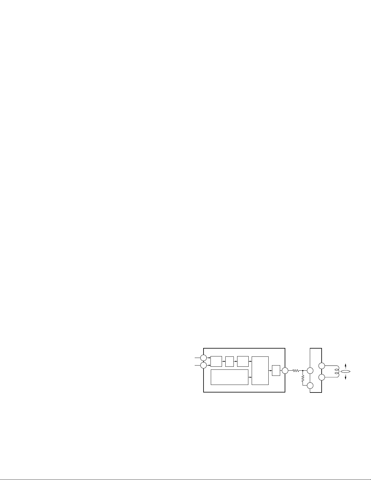
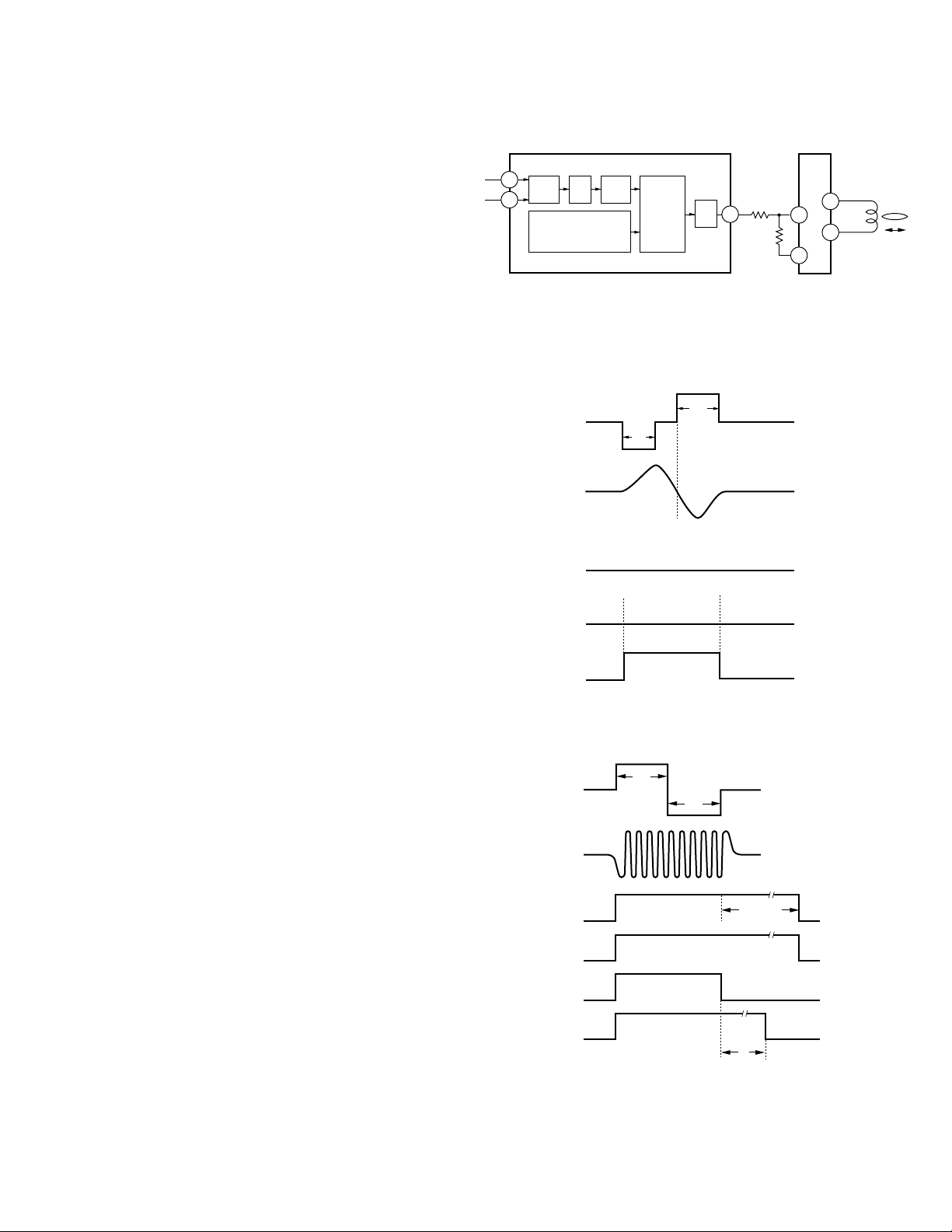
1.5 MECHANISM OPERATION
1) Elevation Operation
The microcomputer determines the present elevation
position from the voltage value (EPVO) obtained from
the potential divider VR801.
The voltage of the position of the requested disk is calculated from figure 20 and the ELV Motor is controlled
so that the EPVO voltage is matched to the value
obtained from the calculation.
2) Tray Extension and Retractino
The microcomputer detects the DSP signal waveform
(voltage) and TRP signal waveform (voltage) obtained
at the DSP switch (S852) and the TRP switch (S851) by
tray retraction, tray extension and clamp completion
and controls the Tray Motor.
EJECT Voltage position EREF+446LSB
DISC1 Voltage position EREF+367LSB EREF+377LSB EREF+387LSB
DISC2 Voltage position EREF+260LSB EREF+270LSB EREF+280LSB
DISC3 Voltage position EREF+193LSB EREF+203LSB EREF+213LSB
DISC4 Voltage position EREF+125LSB EREF+135LSB EREF+145LSB
DISC5 Voltage position EREF+ 58LSB EREF+ 68LSB EREF+ 78LSB
DISC6 Voltage position EREF+ 0LSB EREF+ 0LSB EREF+ 0LSB
DISC7 Voltage position EREF- 78LSB EREF- 68LSB EREF- 58LSB
DISC8 Voltage position EREF-145LSB EREF-135LSB EREF-125LSB
DISC9 Voltage position EREF-213LSB EREF-203LSB EREF-193LSB
DISC10 Voltage position EREF-280LSB EREF-270LSB EREF-260LSB
DISC11 Voltage position EREF-348LSB EREF-338LSB EREF-328LSB
DISC12 Voltage position EREF-416LSB EREF-406LSB EREF-396LSB
[
[
[
[
[
[
[
[
[
[
[
[
[
EPVO
H
L
MAG
* 1LSB=approx 4.88mV (5/1024V)
min typ max
[
]
[
]
ON
OFF
OFF
ON
TRP switch
DSP switch
Tray retracted
Tray in transition
Clamp completed
Fig. 20
Page 17

17
C X-938
3) 0.6mm UP/DOWN Operation
In order to secure clearance with the neighboring disk
the Stage Mechanism is driven down by the ELV Motor
(M852) when clamping is complete. The microcomputer
detects the completion of clamping, and when the Tray
Motor is brought to a full stop, the ELV Motor (M852) is
forcibly driven for a 240 ms interval in the downward
direction.
When the tray is being retracted, the ELV Motor (M852)
is controlled to match the value of EPVO calculated
during the elevation operation. The tray retraction operation is started when the Tray has been moved to the
prescribed position.
Each motor is driven by the driver IC302 (LB1836M).
LB1836M is an IC which usually operated through the
combination of H and L of the 4 lines l1, l2, l3 and l4.
With this system, l1=l3 and control is realized through a
combination of H and L of the 3 lines l1, l2 and l4.
4) Disc Detection
The DSP signal waveform (voltage) at the DSP switch
(S852) is used for determinating the existence and nonexistence of a disk and the disk type (8cm or 12cm). The
disk detection operations are carried out while the Tray
is being pulled out of the magazine. Disk detection is
determined when the light passes through (DISC
waveform L:less than 2.5v) or is interrupted (DISC
waveform H:2.5V or above) with an array of LEDs and
photo transistors above and below the Tray.
The DISC waveform is continuously monitored within
the intervals A and B above and if a L is detected even
once, that interval is determined as L. If a L is not detected at all then that interval is determined as H in the
following.
[
[
]
]
OFF
ON
DSP switch
DISC(12cm)
DISC(8cm)
DISC(Tray only)
AB
40msec
ELV Motor Tray Motor l1,l3 l2 l4
Forward Brake H H L
Reverse Stand-by L L H
Brake Forward H L H
Stand-by Reverse L H L
Brake Brake H H H
Stand-by Stand-by L L L
* ELV Motor Forward : ELV-up (Disc No. Down)
Tray Motor Forward : Tray Ejection
12cm
8cm
No Disk
A
B
Page 18

18
C X-938
Cautions on Service
1) Do not hold the upper frame of the magazine insertion port in the CD mechanism module, marked by an arrow in
Fig. 21, when servicing. It's because this section is easily deformed.
2) The stage mechanism section projects below the chassis when positioned at the tenth stage or lower. So, do not
leave the stage mechanism section at these positions to avoid damage or malfunction.
3) Before removing the flexible card and pickup flexible PCB from the connectors on the relay PCB, be sure to insert a
short pin into the pickup unit first.
4) When replacing the tray motor assy, mount the 2-stage gear(Not resable) on the shaft of a new tray motor assy. (As
the gear uses snap-on fittings, push it in until it is snapped completely.)
5) When replacing the magazine holder assy, mount the worm wheel(Not resable) on the shaft of a new elevation
worm wheel.
(As the gear uses snap-on fittings, push it in until it is snapped completely.)
2. DISASSEMBLY
- Removing the Pickup Unit
1. Insert a short pin into the pickup flexible PCB.
2. Remove the pickup flexible PCB from the connector.
3. Remove the flexible card from the connector.
4. Remove the lead wires of the spindle motor assy and carriage motor assy by removing solder.
5. Loosen the two screws. Lift up the relay PCB as shown in Fig. 22.
Be careful not to excessively pull the tray motor flexible PCB and the relay flexible PCB.
Fig. 21
CD mechanism module
Fig. 22
Flexible card
Erect
Flexible PCB (*Handle
with care)
Tray motor
flexible PCB
(*Handle with
care)
Short Pin
Relay PCB
This section is easily deformed.
Page 19

19
C X-938
6. Remove three screws A and then remove the carriage motor assy, remove the lighting conductor ,feed screw holder,
feed screw and belt (see Fig. 23).
7. Remove screw C on the main side and the pickup unit together with the guide shaft (see Fig. 23).
- Removing the CD Core Unit
1. Insert a short pin into the pickup flexible PCB.
2. Remove the flexible card from the CD core unit connector.
3. Remove the lead wires of the elevation motor assy that were soldered to the CD core unit.
4. Remove screw D and three screws E and then the CD core unit (see Fig. 24).
- Cautions on Mounting the CD Core Unit
When mounting the CD core unit on the CD mechanism module, accurately insert the
linear position sensor (Slide control: VR801) mounted on the CD core unit into the Ushaped groove of the elevation front lever (see Fig. 35).
If the linear position sensor is not inserted into the U-shaped groove, elevation operation
will malfunction.
- Removing the Carriage Motor Assy
After removing the pickup unit (see "Removing the Pickup Unit" in pages 17 and 18),
remove the feed screw, belt ,and feed screw holder.
Fig. 24
Screw E
CD core unit
Screw D
Screw E
Screw E
Mechanism unit - bottom view
Screw A
Motor bracket
CRG motor
Screw B
Feed screw holder
Feed screw
Guide shaft(main)
Guide shaft(sub)
Belt
Screw C
Pickup unit
Fig. 23
Lighting conductor
Page 20

20
C X-938
- Removing the Spindle Motor Assy
1. Rotate the tray motor until the clamp joint arm moves.
2. Slide and remove the clamp spring as shown in Fig. 25.
3. Remove the clamper.
4. As shown below, match the positions of the holes of the support wheel and screws F. Then remove the two screws F
and spindle motor assy.
* When removing the clamper, be careful not to lose the ball mounted between the clamper and clamp spring.
- Cautions on Mounting the Spindle Motor Assy
1. Mount the spindle motor assy so that the lead wires face the rear of the mechanism unit (see Fig. 26).
2. Check that the torsion spring presses the side pressure plate (see Fig. 27).
3. When mounting the clamper, confirm that the ball has been installed.
Fig. 26
Fig. 27
Fig. 25
Front side (magazine insertion port)
Support wheel
Torsion spring
Side pressure plate
Mechanism unit - bottom view
Rear
Clamp spring
Release the clamp spring from the
hook(s), and then slide it in the
direction indicated with an arrow.
Clamper
Match the positions of the
holes and screws F.
Screw F
Support wheel
Screw F
Orientation of the lead wire
Ball
Spindle motor assy
Spindle
motor
assy
Lift here
Clamper
Clamp joint
arm
Page 21

21
C X-938
- Removing the Tray Motor Assy (see Fig. 28)
1. Remove screw G.
2. Remove the elevation joint arm spring.
3. Remove the polyslider washer and the 2-stage gear.
4. Move the front lever to move the stage mechanism unit to the "4" position on the front lever.
5. Remove screw H.
6. Move the front lever again to move the stage mechanism unit to the uppermost stage.
7. Remove the tray motor assy.
- Cautions on Mounting the Tray Motor Assembly (see Fig. 28)
When mounting the 2-stage gear, verify that the positions of the holes of the 2-stage gear
and the stage chassis match each other. For easy confirmation, check that the shapes of the 2-stage gear and the stage
chassis form a concentric circle, as shown in the figure.
- Removing the Elevation Motor Bracket Assy (see Fig. 28)
1. Remove the elevation joint arm spring.
2. Remove the polyslider washer and the 2-stage gear.
3. Remove two screws I and the elevation motor bracket assy.
Fig. 28
Shape of the 2-stage gear
Shape of the stage chassis
Polyslider
washer
2-stage gear
Elevation joint arm spring
Stopper
Magazine
lock spring
Screw I
Elevation motor
bracket assy
Screw I
Screw G
Polyslider
washer
Front frame
Screw H
Front lever
Match the edge of the
front frame and the
reading "4" on the
front lever.
Tray motor assy
Front lever
Page 22

22
C X-938
- Removing the Stage Mechanical Unit Section (see Fig. 29)
1. Remove the elevation joint arm spring.(See Fig. 28)
2. Remove the magazine lock spring.(See Fig. 28)
3. Remove the 2-stage gear.(See Fig. 28)
4. Remove the screw J and then the stopper.
5.Fully slide the front lever in the direction that the stage mechanism assy moves upwards. Then, the front lever and
the rear lever can be removed at the same time.
6. Remove three screws K and two screws L, and then the magazine holder Assy.
7. Remove four screws M and then the lower frame.
8. Remove three screws N and then the front frame.
9. Move the stage mechanism assy to the lowest position. Slide the bent section of the stage mechanism assy along
the L-shaped groove in the front frame to remove the stage mechanism assy.
Fig. 29
Front frame
Screw N
Screw N
Screw L
Screw K
Screw K
Stopper
Screw N
Screw M
Screw M
Lower frame
Magazine
holder Assy
Screw J
Screw K
Screw M
Screw M
Screw L
Rear view of the CD
mechanism module
with the front and rear
levers removed.
Front frame L-shaped groove
Move to this position
Stage bent section
Page 23

23
C X-938
3. MECHANISM DESCRIPTIONS
- Inserting the Magazine
1. When the magazine is inserted against the force of the EJECT lever spring, the lock arm comes in along the groove
in the rear side of the magazine to lock (see Fig. 30).
2. The magazine lock is detected when the detection arm moves along the EJECT lever cam section and presses the
magazine detection switch mounted on the CD core unit.
When the magazine is not inserted, the detection arm is held at the SW OFF position by the EJECT lever cam (see
Fig. 31).
When the magazine starts insertion, the lock arm starts moving along the groove in the rear of the magazine. Then
the lock arm stops at the detection arm "stop" position. Although the detection arm tries to move in the SW ON
direction, the lock arm stops it. (See Fig. 32.)
When the magazine is completely inserted, the magazine to lock. At the same time, the detection arm is released to
press the magazine detection switch with spring force. (See Fig. 33)
Fig. 30
Fig. 31 Fig. 32 Fig. 33
EJECT lever cam
Magazine detection
switch
Detection arm
Lock arm
Stop
Stop
SW ON
Moves along
the groove in
the magazine.
Located at the lock
position along the groove.
When the magazine is not inserted
After the magazine has been inserted
Magazine
Lock arm
EJECT lever
EJECT spring
Lock arm
Groove in the rear of
the magazine
When the magazine is locked
Direction of the magazine insertion
Page 24

24
C X-938
- Elevation Operation (see Fig. 34)
When the elevation motor is driven, the elevation joint arm rotates. The front and rear
levers, engaged with the ends of the elevation joint arm respectively, slide to move the
stage mechanism unit up and down.
- Detecting Elevation (see Fig. 35).
When the elevation joint arm rotates, the front lever slides.
Because the knob of the linear position sensor (slide control: VR801) is inserted in the U-shaped groove of this front
lever, the elevation joint arm moves in synchronization with the lever and detects the voltage at that time.
Fig. 34
Fig. 35
Linear position sensor (Slide
control: VR801)
Front lever
Front leverShaft
Bottom view
Rear leverShaft
Stage mechanism unit
Elevation
joint arm
Stage mechanism unit
Page 25

25
C X-938
- Tray Extraction to Clamp Operation (Loading Motor Drive Section) (See Fig. 36.)
When the loading motor drives the cam gear, the cam gear moves the tray extraction arm along the cam groove to
extract the tray. At that time, the carriage assy (including the spindle motor assy and tray positioning pin) waits until
the tray passes it. When tray extraction has been completed, the cam gear swings the clamp joint arm and slides the
clamp lever engaged with the clamp joint arm. The shaft of the carriage assy is lifted along the step-shaped groove as
the clamp lever slides. The carriage assy swings toward the stage chassis. Subsequently, the spindle motor assy
comes to a CD disc to load and lift it up from the tray.
Fig. 36
Clamp spring
Clamper
CD
Tray
Spindle
motor assy
Carriage assy
Carriage chassis
Waiting state
Stage chassis
Tray
Clamp joint arm
Cam gear
Clamper
Spindle motor assy
Carriage chassis
Shaft
Positioning pin
Clamp lever
Tray extraction arm
Clamp position
Page 26

26
C X-938
- Elevation Mechanism - Play Elimination
Immediately before the clamp operation is completed, the bent sections of the clamp lever comes into the frame
stopper section and press it downward to control the vertical position. This operation can press the stage downward
by means of the elevation mechanism. At this time, the elevation motor stops, not by the detection of the pressed
position, but in a certain period of time after the elevation mechanism moves up to the limit of the movement. (See
Fig. 37)
The figure 37 shows the pressing mechanism. When the clamp lever bent sections press the framestopper section, the
carriage chassis shaft inserted into the clamp lever groove is lifted up until it is pressed against the end of the vertical
groove in the stage chassis. At this time, the stage chassis shaft, which is also inserted into the other groove in the
clamp lever, is located at the wider portion of the groove so that the carriage chassis shaft can move to the end of the
vertical groove in the stage chassis. This pressing operation eliminates the play at each of the stage chassis, carriage
chassis, clamp lever, and the frame to improve the resistance against vibration. (See Fig. 39.)
* The elevation joint arm spring has been installed to keep this pressing state.
- Disc detection
The cam gear for tray extraction operation moves the DSP switch lever to turn the DSP switch (S852) ON and OFF. The
photo sensors (Q851 and D852) detect the presence of discs and their types (8 or 12 cm) with a certain timing.
Fig. 37
Clamp lever
bent section
Clamp lever
bent section
Clamp lever
bent section
Frame stopper
Stage chassis vertical
groove end
Stage chassis shaft
Carriage chassis shaft
Frame stopper
Clamp lever
The play of each
section is eliminated
by pressing the
sections marked by
circles.
Stage
chassis
Carriage
chassis
Looseness
After being pressed
Before being pressed
Gaps
Total amount of
carriage shaft
looseness
Fig. 38
Fig. 39
Page 27

27
C X-938
- Detecting Tray Extraction and Return
A) Tray extraction (Fig. 40)
The clamp joint arm moves the clamp lever and performs clamping. After clamping has been completed, the
protrusion on the clamp joint arm presses the TRP switch (S851) via the TRP switch (S851) via the plate spring on
the DSP switch lever and turns on the switch.
B) Tray return (see Fig. 41)
The TRP switch (S851) is turned on by the DSP switch lever moved by the cam gear.
Fig. 40
Fig. 41
DSP switch lever
LED (D851)
DSP switch (S852)(ON)
TRP switch (S851)(ON)
Cam gear
Clamp lever
Clamp joint arm
DSP switch (S852)(OFF)
TRP switch (S851)(ON)
Page 28

28
C X-938
- Tray Lock Mechanism
In other modes than the PLAY mode, the tray bouncing prevention spring is deflected by the rear lever and functions
as a stopper to prevent the tray from coming out of the magazine. (Fig. 43)
In the PLAY mode, the window in the rear frame catches the projection of the tray bouncing prevention spring.
Accordingly, the spring is not deflected to enable the tray's insertion and extraction. (Fig. 42)
Consequently, in other modes than the PLAY mode (during the waiting mode), the tray will not come out of the
magazine even if external shock is applied to it. (Fig. 43)
- Ejecting the Magazine (see Fig. 44)
When the rear lever is further driven from the uppermost stage position of the elevation, the bent end face of the rear
lever presses the boss on the lock arm to release the lock and the magazine is ejected by the EJECT lever.
Fig. 42
Fig. 43
Fig. 44
Lock arm
Boss
Rear lever
When set in the
PLAY position
When set to a position
other than PLAY
Functions as a stopper
Rear lever
Tray
Bouncing
prevention spring
Window
Page 29

29
C X-938
- Lubrication points (Fig. 45)
(3) For the other sections, use the E paste.
Fig. 45
Feed screw tip
Pickup Unit
Sub guide shaft
(1) Around the pickup assy ->
Use EM-60L for all points.
(2) Slide section with clamp ball
Main shaft
Feed screw tip
Feed screw
thread
Spacer
Clamper
EM-60L (Dow
Corning)
Clamp spring
 Loading...