

Page 1

PIONEER ELECTRONIC CORPORATION 4-1, Meguro 1-Chome, Meguro-ku, Tokyo 153-8654, Japan
PIONEER ELECTRONICS SERVICE INC. P.O.Box 1760, Long Beach, CA 90801-1760 U.S.A.
PIONEER ELECTRONIC [EUROPE] N.V. Haven 1087 Keetberglaan 1, 9120 Melsele, Belgium
PIONEER ELECTRONICS ASIACENTRE PTE.LTD. 501 Orchard Road, #10-00, Wheelock Place, Singapore 238880
C PIONEER ELECTRONIC CORPORATION 1998
K-ZZB. OCT. 1998 Printed in Japan
ORDER NO.
CRT2291
MD MECHANISM MODULE
CX-893
CONTENTS
1. CIRCUIT DESCRIPTIONS...........................................2
2. DISASSEMBLY.........................................................13
- This service manual outlines operations of the MD mechanism module used in the models listed
below.
- For repair, use this Service Manual and the Service Manual of the model used in the system.
Model Service manual MD mechanism module
MEH-P5000R/EW CRT2287 CXB2784
Page 2
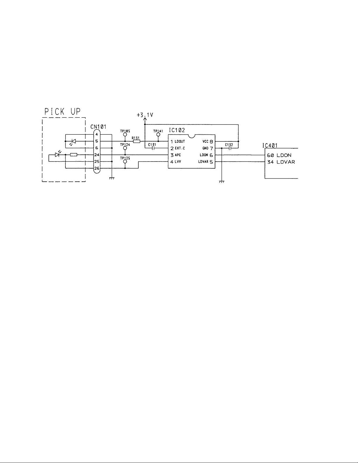
Figure 1 below shows the block diagram. This block
controls the output from the block LD to be consistent
with the monitor diode.
The block consists of IC 102 and turned to LD ON when
LDON (6 pin) is H and to LD OFF when LDON is L. LD
output level is set with the voltage value of LDVAR and
is usually around 2.4 V.
2
CX-893
1. CIRCUIT DESCRIPTION
1.1 APC Part
Fig.1
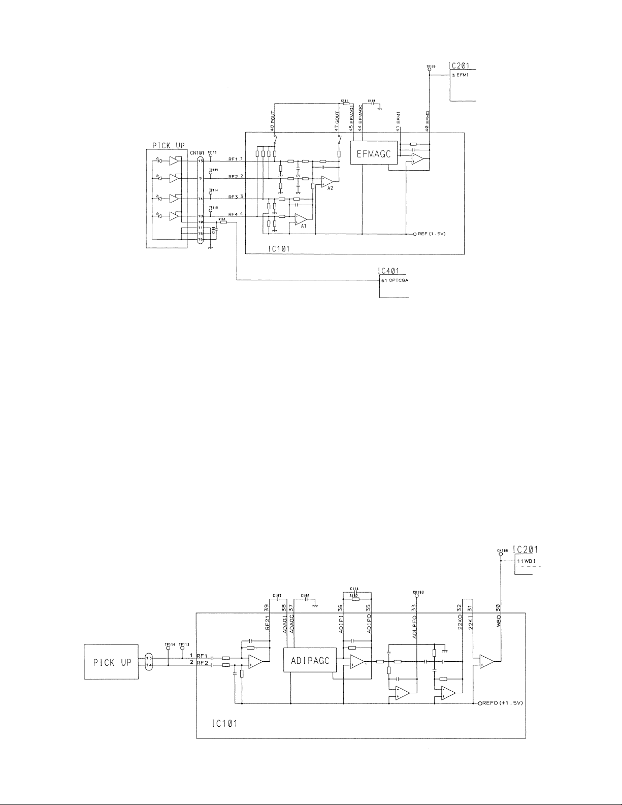
1.2 RF amplifying part
The block amplifies the pickup output signal and
generates RF and ADIP signals.
This block mainly consists of IC101.
REFO part
REFO (+1.5 V) is the reference voltage for the servo.
The signal is resistive divided at the IC (REFI: 5 pin) and
output to 6 pin through buffer. This signal will be the
reference for RFIC.
RF signal amplifying part
Figure 2 below shows the block diagram. The signal
which is I-V converted at the pickup is input to the RF1-4
(1-4 pin). Gain at the I-V amplifier contained in the PU
is switched depending on the disc types. The switching
is controlled by OPICGA (IC401, 61 pin) and H is output
at Premaster DISC and L is output at Recordable DISC.
The signal input from the I-V amplifier is operated with
the contained resistance and amplifiers (A1, A2) and the
signal (RF1 + RF2 + RF3 + RF4) (POUT) and the signal
(RF1 + RF2 + RF3 - RF4) (GOUT) are generated. Each of
POUT and GOUT is equipped with an analog switch.
The switches are controlled with the DISC signal (bits
on microprocessor serial communications). The POUT
signal is output through 48 pin when the DISC signal is
H (PIT mode) and GOUT signal is output through 47 pin
when the DISC signal is L (GRV mode).
These signals are input to EFMAGC (45 pin) through the
coupling capacitors (C133, C112) and transmitted to the
AGC circuit and filter part to be output from EFMO (40
pin). The EFMO is maintained at almost same level
(approx. 1.5 Vpp) with the AGC circuit. These signals
are input to the signal processing part (IC201: 3 pin) and
used for data processing and spindle control when
playing a Premaster Disc.
Page 3
3
CX-893
Fig.2
ADIP signal amplifying part
Figure 3 shows the block diagram of this part. The block
generates the ADIP signal which exists only on a
Recordable DISC of a MD.
Signals input to RF1 and RF2 (1,2 pin) are transmitted
through the AGC part and the filter part to be output to
22KO (32 pin). The 22KO is designed to be maintained
at almost same level (approx. 1.2 Vpp) with the AGC
circuit. However, fluctuation of about +0.5V may be
observed due to core components, responsibility of
tracking servo, etc. The signal is then converted to 1
and 0 signal with the comparator C1, input to the signal
processing part (IC201:11 pin), and used for address
control when playing disc for recording and spindle
control.
*Will not be used when Premaster Disc is played.
C1
Fig.3
Page 4
4
CX-893
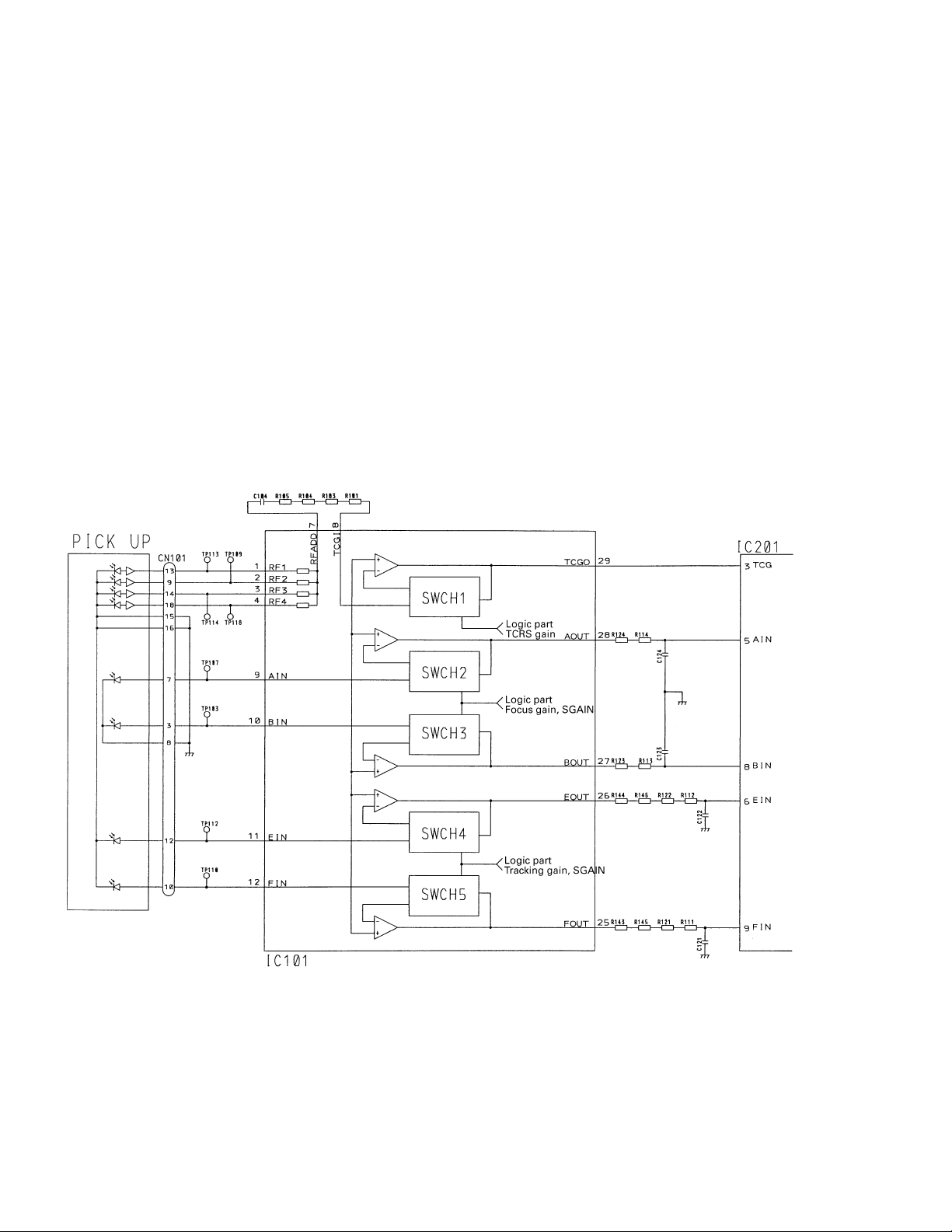
Track cross part, signal amplifying part for servo
Figure 4 shows the block diagram of these parts.
The signal input to RF1-4 (1-4 pin) is resistive divided
and amplified to be output to TCGO (29 pin). TCGO is
input to the signal processing part (IC201:7 pin) and
TCRS signal is generated and will be used when the
system skips tracks to play.
Outputs from the focus servo based photo diode are
input to AIN (9 pin) and BIN (10 pin) and are output to
AOUT (28 pin) and BOUT (27 pin), respectively, after
being amplified.
Outputs from focus servo based photo diode are input
to EIN (11 pin) and FIN (12 pin) and are output to EOUT
(26 pin) and FOUT (25 pin), respectively, after being
amplified .
These signals are input to the signal processing part
(IC201: 5,6,7,8,9 pin) and used at each servo.
Amplifying ratios of each signal are controlled by the
microprocessor and adjusted so that they reach
optimized values when mechanical modules are
shipped. Those optimized values are stored in IC402.
Therefore, when you replace IC or PU switch, etc., you
should have the IC402 memorize new optimized values
by turning EEPROM (IC402) to write mode (See the
relevant sections for details.) and running test modes
AUTO1 and AUTO2 with a Recordable DISC (MMD-211
or MMD-212).
Fig.4
Page 5

5
CX-893
Logic part
Serial commands of the microprocessor determines the
setting of this IC.
Timing chart
DATA (23pin)
CLOCK (22pin)
LATCH (21pin)
MSB 7SB 6SB 5SB 4SB 3SB 2SB 1SB
Structure of serial data
MSB 7SB 6SB 5SB 4SB 3SB 2SB 1SB
Pattern A H L Focus gain Tracking gain
Pattern B L H STBY DISC SGAIN Track loss gain
Gain setting (+12dB when SGAIN=H at normal operation)
Setting value Focus gain Tracking gain Track loss gain
000 –40 –40 –18
001 –34 –34 –12
010 –28 –28 –6
011 –22 –22 0
100 –16 –16 6
101 –10 –10 12
110 –4 –4 18
111 –4 –4 18
STBY: Switches to stand-by mode
H: Normal L: Stand-by
DISC: Switches to disc mode
H: PIT (Premaster Disc)
L: GRV (Recordable Disc)
SGAIN: Switch of amplifier gain for servo
H: +12dB
L: Normal
Page 6

6
CX-893
1.3 Signal processing part (IC201)
This block consists of the following four parts:
1) Servo part
2) Signal processing part
3) Shock proof controlling part
4) ATRAC part
The details for each part are described below.
1) Servo part
1.1) Focus servo
Figure 5 shows the block diagram of the focus servo.
The signals input to AIN (5 pin) and BIN (8 pin) are
processed with subtraction treatment after analogdigital conversion. These signals can be monitored
with FEMON (75 pin). These signals, however, should
be monitored using LPF with cutoff of around 50 kHz
(e.g. R=100 kΩ, C=33 pF) because they are PWM signals.
These signals are equalized at subsequent D and F parts
and output to FODRF (18 pin) and FODRR (19 pin) with
PWM.
The output signals are amplified with the driver (IC601)
and drive the actuator.
You must move the lens up and down for close focus.
Close the focus when the following requirements are
met:
1) When the lens is going down.
2) FOK (82 pin) = L
3) FZC (signal inside IC ) = i
Fig.5
Page 7

7
CX-893
1.2) Tracking servo and thread (carriage) servo
Figure 6 shows the block diagram of the tracking servo
and thread (carriage) servo.
1.2.1) Tracking servo
Signals input to EIN (6 pin) and FIN (9 pin) are
processed with subtraction treatment after analogdigital conversion. These signals can be monitored
with TEMON (75 pin). These signals, however, should
be monitored using LPF with cutoff of around 50 kHz
(e.g. R=100 kΩ, C=33pF) because they are PWM signals.
These signals are equalized at subsequent D and F parts
and output to TRDRF (20 pin) and TRDRR (21 pin) with
PWM. The output signals are amplified with the driver
(IC601) and drive the actuator.
1.2.2) Thread servo
Thread servo extracts and amplifies only low frequency
signals by transmitting the outputs from tracking D and
F parts through D and F parts. When these signals
exceed a certain threshold voltage, they are output to
SLDRF (22 pin) and SLDRR (23 pin) with PWM.
These signals are amplified with the driver (IC601) and
then drives the motor.
Fig.6
Page 8

1.3) Track jumping
Tracks to play are automatically skipped using AUTO
mode which is an LSI function.
Figure 7, 8, and 9 show examples of 1TJUMP, 10JUMP
and Auto MOVE, respectively.
8
CX-893
Antiskid
SLKLEV
WAIT
SLCT
Automove
Antiskid
SENSE (terminal)
Tracking output
Tracking count
(COUT) : the no. of
tracks = TRCNT x 64
Thread output
Specified no. of tracks
Fig.7
Fig.8
Fig.9
TE
Tracking
drive output
SENSE (terminal)
TE
Tracking
drive output
SENSE (terminal)
Page 9

1.4) Spindle servo
Figure 10 shows the block diagram of the spindle servo.
Perform CLV control with EFMI (3 pin) when you play
the read-in area of a Premaster DISC or Recordable
DISC and with WBI (11 pin) when you play the program
area of a Recordable DISC.
1.5) Auto tuning
This mechanical module is automatically tuned so that
it absorbs dispersion among discs caused by ambient
changes or course of time thereby stabilizing the play of
discs. This auto tuning will be made whenever you
insert a disc or select MD mode with the source cue.
1.5.1) When you play Premaster DISC
Tracking ATT tuning
Measures the levels of LPFEINO, LPFFINO and EFMIO
that EIN (6 pin) and FIN (9 pin) generate and specifies
the amount of ATT that is calculated with formula.
u
Maintains the tracking loop gain at a certain level and
stabilizes the tracking servo operation.
Focus ATT tuning
Measures the levels of LPFABO that AIN (5 pin) and
EIN (8 pin) generate and specifies the amount of ATT
that is calculated with formula.
u
Maintains the focus loop gain at a certain level and
stabilizes the tracking servo operation.
1.5.2) When you play a Recordable DISC
Tracking ATT tuning (PIT. GRV)
Measures the levels of LPFEINO, LPFFINO and EFMIO
that EIN (6 pin) and FIN (9 pin) generate and specifies
the amount of ATT that is calculated with formula.
u
Maintains the tracking loop gain at a certain level and
stabilizes the stabilizes the tracking servo operation.
Focus ATT tuning (PIT. GRV)
Measures the levels of LPFABO that AIN (5 pin) and
EIN (8 pin) generate and specifies the amount of ATT
that is calculated with formula.
u
Maintains the focus loop gain at a certain level and
stabilizes the tracking servo operation.
TCRS ATT tuning
Measures the level of TCGSMIO that TOG (7 pin)
generates and specifies the amount of ATT that is
calculated with formula.
u
Stabilizes searches when you play a Recordable DISC.
9
CX-893
Fig.10
Page 10

2) Signal processing part
Figure 11 shows the block diagram of signal
processing, shock proof controlling and ATRAC parts.
The signal processing part consists of the two blocks,
one of which demodulates the music data on the disc
and corrects errors, and the other of which controls
addresses used for searches and time calculation.
2.1) Music data
The signal input from EFMI (3 pin) is equalized with the
digital filter after analog-digital conversion. This signal
can be monitored with EFMO (1 pin). The signal will be
sliced at an appropriate level and modulated to 0 and 1
signal and then transmitted to the subsequent shock
proof part after EFM demodulation and error correction
are completed.
2.2) Address control
Reads the address data on the disc and specifies targets
for time control during play and searches. The
methods of reading the address data depends on the
disc types.
When you use a Premaster DISC
Extracts the address data from the music data after
error correction is completed.
When you use a Recordable DISC
Modulates frequency of the signal input from WBI (11
pin) and reads the addresses from the data.
3) Shock proof controlling part
The data from the signal processing part is temporarily
stored in DRAM (IC202). Later, the data will be sent out
sequentially by the data requests from the subsequent
ATRAC part or instructions from the microprocessor.
This mechanical module contains the 4MB DRAM and
can store the data of approximately 10 seconds.
4) ATRAC part
The data from DRAM (IC202) will be extended for
ATRAC at this block and then converted into the audio
data.
The data formats to be used at the subsequent DAC
(IC501) are as follows:
BCLK (71 pin): 64 Fs
DADATA (74 pin): 20 bits from the last
DFCK (72 pin): 256 Fs
LRCK (70 pin): Fs, L/R
*Fs=44.1 kHz
10
CX-893
Fig.11
Page 11

1.4 Mechanical control
1) Loading
The microprocessor instructs the motor driver IC651 to
rotate backward (IC651: 3 pin: L, 4 pin:Ht¨L+: L, L-:H) if
LOAD STRAT SW (SW652) detects OFF (LOAD
STRAT=H). If LOAD STRAT SW (SW652) detects ON
(LOAD END=L) later, the microprocessor instructs the
motor driver IC651 to stop (IC651: 3pin: H, 4pin:Ht¨L+:
L, L-:H) and completes the loading and then transits to
PLAY operation. If DISC IN SW (SW903) is OFF (DISC
IN=H) or LOAD END SW has been OFF for a long time,
the microprocessor determines that there is no inserted
disc or a disc insertion error and performs EJECT or
Error STOP.
2) EJECT
The microprocessor instructs the motor driver IC651 to
positively rotate (IC651: 3 pin: H, 4 pin:Lt¨L+: H, L-:L)
when it receives the EJECT instruction. If EJECT END
SW (SW653) detects ON (EJECT END=L) later, the
microprocessor instructs the motor driver IC651 to stop
(IC651: 3pin: H, 4pin:Ht¨L+: H, L-:H) and completes the
EJECT operation.
11
CX-893
1.5 Others
1) Temperature detection
This module detects high temperatures, to protect PU.
When the temperature of the output from the
temperature sensor (IC402) exceeds a certain voltage
level, it is determined as high temperature and an
appropriate process such as Error STOP will be
performed. The ambient temperature which causes
that high temperature on the module is approximately
80 degree Celsius.
2) Voltage monitoring
This module monitors voltage to protect the system.
The signals which are resistive divided (R803, 804) from
the input VD from the product (CN301: 1,2) are
monitored (IC401, 25 pin). If the voltage of the signal is
higher than 2.86 V (VD7V or higher) or lower than 2.04
V (VD5V or lower), an appropriate process such as Error
STOP will be performed.
Page 12

12
CX-893
1.6 How to rewrite EEPROM
This mechanical module stores adequate values for the
servo, etc., in the EEPROM (IC402). Therefore you need
to rewrite the data in the EEPROM when you replaced
mechanism, PU, LSI, or microprocessor.
- When you replaced EEPROM (IC402),
microprocessor (IC401)
1 Make TP435 (IC402: 6 pin) and TP421 (IC402: 8 pin)
short-circuited.
2 Start the product in Test mode. (See manuals for
each product for how to start.)
3 Display the EEPROM setting menu and view any
setting value, e.g., Focus “FGP__XX”. (You should
not change the value.)
4 Switch to Test STOP mode.
5 Turn ACC off. * After turning ACC off, wait for about
10 seconds because EEPROM is written into during
that time.
6 Turn Backup off.
7 Disconnect the short-circuits you have done in the
step 1).
- When you replace pickup, mechanism, LSI
(IC101, 201) or their peripherals.
1 Make TP435 (IC402: 6 pin) and TP421 (IC402: 8 pin)
short-circuited.
2 Start the product in Test mode. (See manuals for
each product for how to start.)
3 Load Recordable DISC (MMD-211 or MMD-212) and
run AUTO1. When “Complete” sign appears, press
the FUNC key and run AUTO2. When “Complete”
sign appears again, press the FUNC key and confirm
the indicated addresses are normally counted up.
*If “Can’t ADJ” sign appears in this step, check the
soldering if it has any problem.
4 Switch to Test STOP mode.
5 Turn ACC off. * After turning ACC off, wait for about
10 seconds because EEPROM is written into during
that time.
6 Turn Backup off.
7 Disconnect the short-circuits you have done in the
step 1).
Page 13

2. DISASSEMBLY
- How to remove mechanism
1. Remove No.3 screws and remove the loading motor.
2. Rotate No.4 gear in the direction indicated by the arrow.
3. Remove the No.1 screw and then No.2 screw and take out the mechanism.
13
CX-893
Fig.12
Fig.13
Page 14

- How to remove the disc motor
1. Remove the connector from the mechanism PCB.
2. Release the three screws and remove the disc motor.
CX-893
- How to remove the sled motor.
1. Remove the two points of solder on the sled motor
terminal.
2. Release the two screws and remove the sled motor.
Note) Be sure not to damage the motor gear.
- How to remove optical pickup
1. Release the three screws.
2. Pull one shaft out a little to the slide motor side and
lift the optical pickup upward slowly.
Disc motor
Mechanism PCB
MD mechanism
Sled motor
x2
Remove the solder
x2
x1
x1
Shaft
Optical pickup
Fig.14
Fig.15
Fig.16
 Loading...