

Page 1
ORDER NO.
PIONEER CORPORATION 4-1, Meguro 1-chome, Meguro-ku, Tokyo 153-8654, Japan
PIONEER ELECTRONICS (USA) INC. P.O. Box 1760, Long Beach, CA 90801-1760, U.S.A.
PIONEER EUROPE NV Haven 1087, Keetberglaan 1, 9120 Melsele, Belgium
PIONEER ELECTRONICS ASIACENTRE PTE. LTD. 253 Alexandra Road, #04-01, Singapore 159936
PIONEER CORPORATION 2009
CRT4300
DVD MECHANISM MODULE(LS1)
CX-3250
- This service manual describes the operation of the DVD mechanism module incorporated in models listed in the table below.
- When performing repairs use this manual together with the specific manual for model under repair.
Model Service manual DVD Mechanism Module
DVH-P4100UB/XN/EW5 CRT4256 CXK6800
DVH-P4100UB/XN/UW5
DVH-P4150UB/XN/RC CRT4282 CXK6800
DVH-P4150UB/XN/RD
DVH-P4150UB/XN/RI
DVH-P4190UB/XN/ID
CONTENTS
1. CIRCUIT DESCRIPTIONS ...............................................................................................................................2
2. MECHANISM DESCRIPTIONS ......................................................................................................................17
3. DISASSEMBLY ...............................................................................................................................................22
K-ZZU. JAN. 2009 Printed in Japan
Page 2
1234
1234
C
D
F
A
B
E
1. CIRCUIT DESCRIPTIONS
1. Front end section (MN2DS0018MAUB : IC1501)
MN2DS0018MAUB is a 1 chip LSI for DVD-Player. A DVD-Player system can be constructed by connecting this LSI,
driver IC, SDRAM, Flash-ROM, Audio-DAC, etc.
This LSI includes a front end (SODC/FE) which executes RF signal processing, servo processing and decode
processing, a AV decoder(back end/BE) which executes video decode processing such as MPEG1/MPEG2/JPEG
and audio decode processing such as DVD-Audio/Dolby Digital /DTS/MP3, and a system controller which controls
the system.
The front end section realizes optical head signal computation processing and RF signal processing, digital signal
processing (16-8 demodulation, error correction) for DVD-ROM playback according to the DVD specifications,
digital signal processing of CD-DA/CD-ROM (error correction), AV decoder transfer, servo control, spindle motor control
and seek control.
In the case of MN2DS0018MAUB, the front end servo system waveforms, such as FE, TE and AS, are not observed
as in the case of DVD mechanism module (MS5) CX-3212. Please pay attention.
1.1 Analog block (MN2DS0018MAUB : IC1501)
The functions of the analog block are as described below.
1. Reference power circuit
2. SERVO system/DPD system signal processing circuit
Gain switching amplifier and Low Pass Filter (LPF)
3. RF signal processing circuit
RF adding circuit, circuit to make inline, Variable Gain Amplifier (VGA) circuit
4. Laser power control (LPC) circuit
5. A/D converter for SERVO (10 bit, DPD system-4ch),DPD converter, PWM
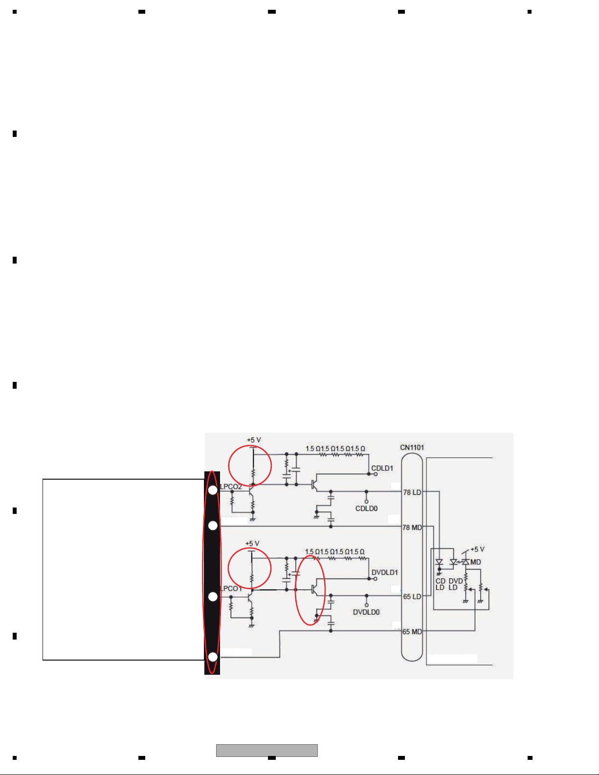
1.1.1 APC circuit
The optical output of the laser diode (LD) has a large negative temperature characteristic.
Therefore, if the LD is driven by a constant current, a constant optical output cannot be obtained.
APC circuit is a circuit to control the current so that the output at the monitor diode (MD) will be constant.
MN2DS0016AAUB includes 2 types of APC circuit, one for DVD and the other for CD.
The LD current can be obtained by dividing the measured voltage between DVDLD1 (CDLD1) and 5 V by 6 Ω
(1.5 Ω x 4=6 Ω), in the case of DVD (CD). It will be approximately 50 mA (45 mA) in the case of DVD (CD).
The potential difference between DVDLD1(CDLD1) and 5 V is set to approx. 300 mV(270 mV).
DV5U Chip
(MN2DS0018MAUB : IC1501)
CDMPD
17
DVDMPD
PU UNIT
2
106
105
104
103
7
8
18
2
CX-3250
Page 3

5 678
56
7
8
C
D
F
A
B
E
ADC
ADC driving AMP
Buffer AMP
Selector
ADC
Selector
Gain switching
6/7.5/9/10.5/
12/13.5/15/
16.5/17/19.5 dB
Gain switching
3 dB, 9 dB
FE
DV5U Chip
AMP
Gain switching
15
G=0 dB
LPF
50 k/100 kHz
-6 dB, 0 dB, 9.5 dB
VIN7
115
14
FE1
Buffer
LPF
LPF
50 k/100 kHz
Input AMP
VIN8
116
FE = (FE1) - (FE2)
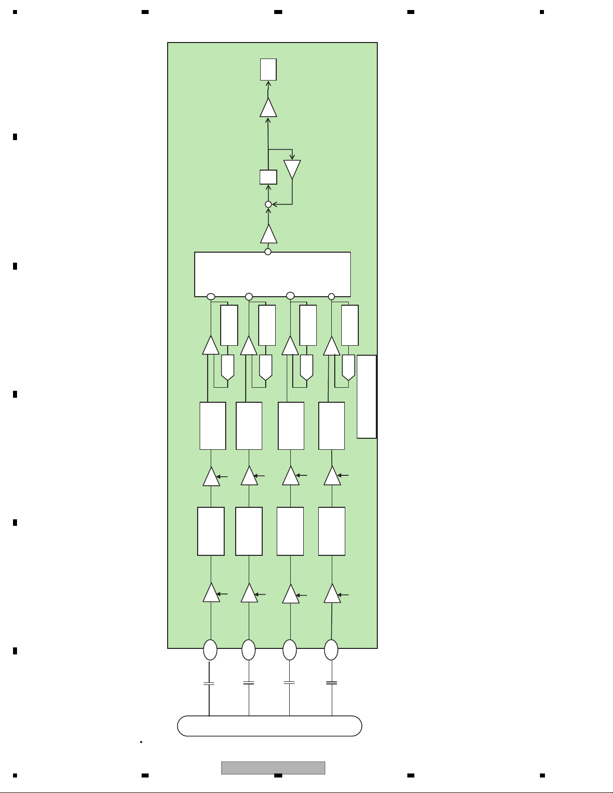
The signal from PU, FE1 and FE2, are AD converted inside IC1501 and captured. After that, a differential is obtained by taking the offset cancellation into consideration,
1.1.2 FE forming circuit
and FE is obtained.
Focus error (FE) forming circuit
CN1101
FE2
FE signal forming circuit
1+Pfbal0,1/0x0100
After 10 bit ADC
CX-3250
FE1
+
-
DV5U Chip
1-Pfbal0,1/0x0100
Fbal coarse adjustment value
Offset cancel
FE2
3
Page 4
1234
1234
C
D
F
A
B
E
1.1.3 TE forming circuit
Tracking error (TE) forming circuit
In the case of a DVD, the phase difference method is used for TE forming, and the TE is formed from the phase difference among (A+C) and (B+D).
In the case of a CD, 3 beam method is used, and after entering the signal into a variable amplifier, it is AD converted,
and a TE is formed by the equation of TE=(F+H_G+H)-(E+G_E+F).
DVD (phase difference TE)
A
B
C
D
CN1101
0.1 μF
0.1 μF
0.1 μF
0.1 μF
10
11
12
13
98
99
VIN3RF
VIN1RF
97
VIN4RF
100
VIN2RF
Gain switching
–7.5 dB, 0 dB, 3.5 dB
LPF
11.3 M
/5.7 MHz
Input AMP LPF
LPF
11.3 M
/5.7 MHz
LPF
11.3 M
/5.7 MHz
LPF
11.3 M
/5.7 MHz
Buffer
Gain switching
G=0,3,6,9,12,15 dB
HPF
HPF
DAC control
Filter
1 MHz/25 MHz
/Through
HPF
1 MHz/25 MHz
/Through
HPF
1 MHz/25 MHz
/Through
HPF
1 MHz/25 MHz
/Through
G=-1 dB
ADCAMP
DV5 Chip
Phase comparator
Phase
comparator
LPF (integrator)
D
+
TE signal forming circuit
AMP
TE
+
DAC
DAC control
Filter
DAC
DAC control
Filter
DAC
DAC control
Filter
DAC
4
CX-3250
Page 5
5 678
56
7
8
C
D
F
A
B
E
ADCSelector
AMP
Buffer AMP
Buffer
LPF
LPF
50 kHz
Selector ADC
G=0 dB
Gain switching
6/7.5/9/10.5/
12/13.5/15/
16.5/18/19.5 dB
Gain switching
3 dB, 9 dB
DV5U Chip
LPF
50 kHz
TE
AMP
+
TE signal forming circuit
1+Ptbal0,1/0x0100
-
DV5U Chip
1-Ptbal0,1/0x0100
Input AMP
VIN9
CD (3 beam TE)
CN1101
112
4
H
F+H_G+
Gain switching
-6 dB, 0 dB, 9.5 dB
VIN10
111
5
E+G_E+F
After 10 bit ADC
F+H_G+H
CX-3250
Offset cancel Tbal adjustment value
E+G_E+F
5
Page 6
1234
1234
C
D
F
A
B
E
1.2 Servo block (MN2DS0018MAUB : IC1501)
At the servo block, focusing, tracking, servo control of traverse, spindle motor control and seek control are performed.
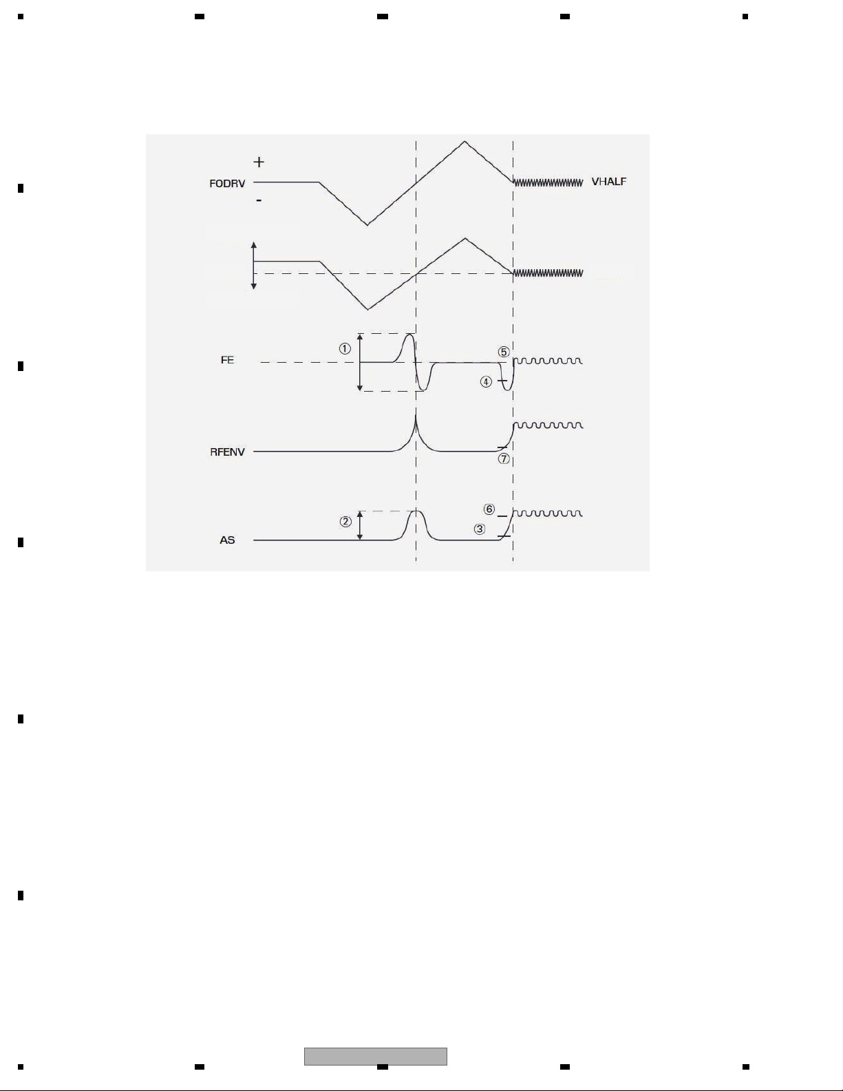
1.2.1 Focus close
After issuing the focus close command, both the DVD and the CD will perform the following processing.
1. Measurement and optimization of the signal level.
First the PU lens is driven in the direction getting away from the disc, then it is driven in the direction getting close
to the disc. At this time, each signal level of FE, AS and RFENV are measured at the focused focal point that the
lens passes, and the levels of FE and AS are optimized. (1 and 2 in the figure)
2. Focus adjustment
Next, after detecting the drawing level of FE and AS by driving the lens away from the disc, the focus loop filter is
activated and the focus is drawn. (3~6)
3. Confirmation of adjustment
Confirm the drawing at the signal level of AS and RFENV. (6, 7)
The signal levels of FE, AS and RFENV and the focus drive voltage can be checked by the focus search in the
test mode.
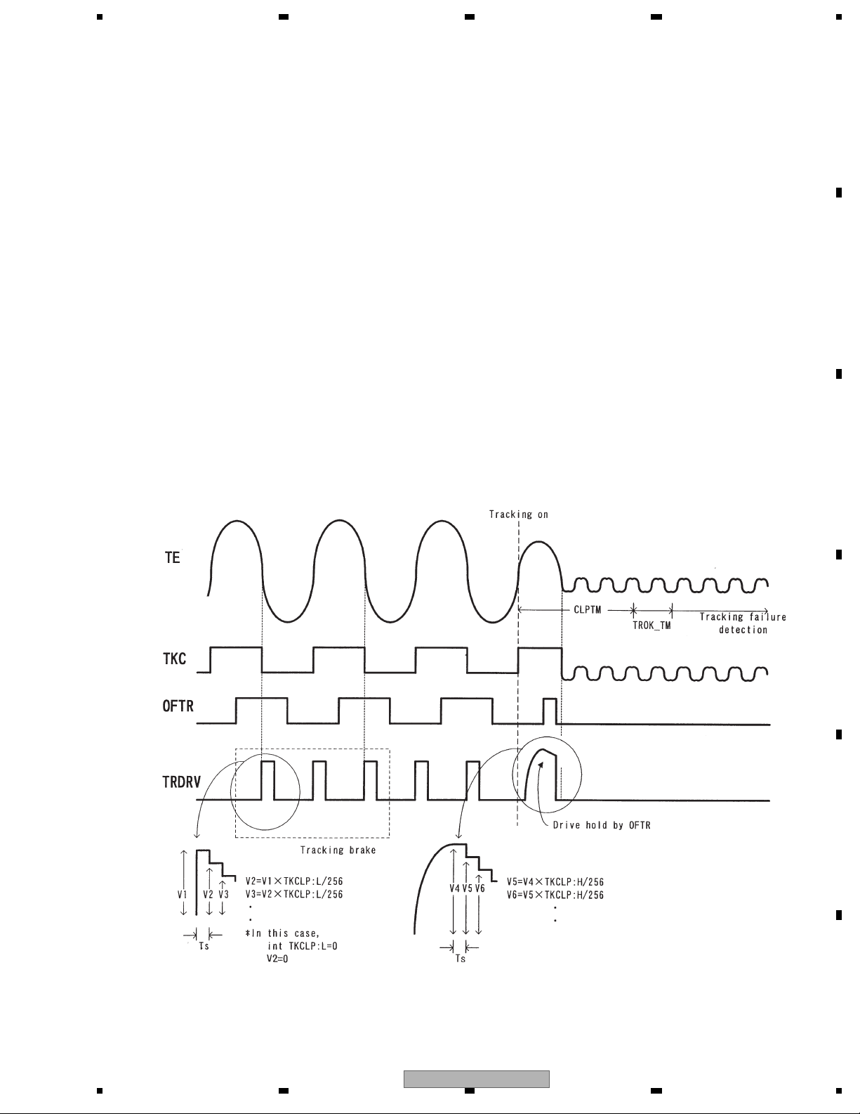
1.2.2 Tracking close
After issuing the tracking close command, both the DVD and the CD will perform the following processing.
1. Tracking brake
1/2 cycle of the track cross is measured and if the cycle is within the specified range, the brake pulse is output.
The output direction of the brake pulse is determined by the phase relationship of the OFTR and the TKC
(binary signal of TE) signals. When it is confirmed that the swinging of the lens against the disc has been controlled,
braking will be stopped and enters into drawing. If the drawing conditions are not met within 10 msec, after the brake
output, the brake will be ended and entered into drawing.
2. Tracking adjustment
Tracking drive hold processing by the OFTR signal will be performed.
3. Confirmation of adjustment
Checking is made that the number of track jumps within the specified period of time are at the designated numbers
or less. The time out for confirmation of adjustment is 8.4 msec. and retry is performed by the command from the
microcomputer.
Close to disc.
Lens
Late
Merging
point
6
CX-3250
Page 7
5 678
56
7
8
C
D
F
A
B
E
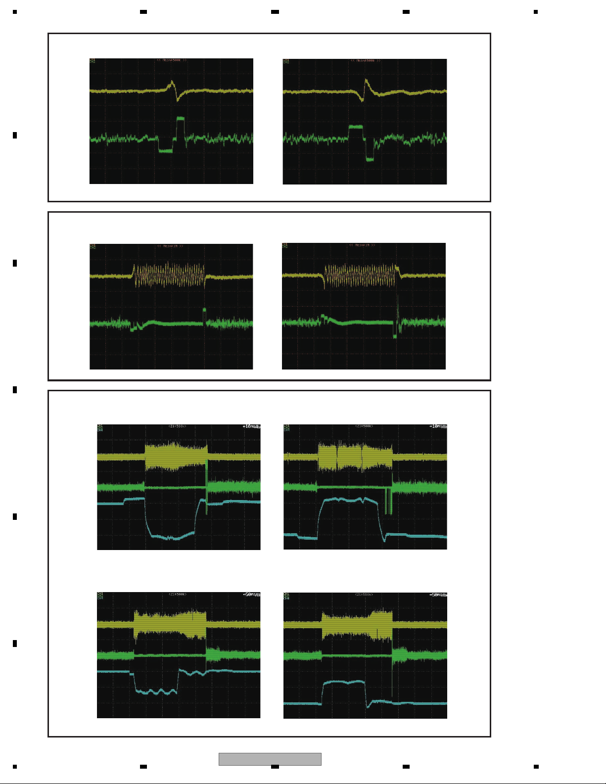
1.2.3 Track jump
In this system, one of the three methods, interval jump, multi jump or traverse seek, is selected depending on the
number of target moving tracks.
1. Interval jump
Detailed seek can be performed to execute repeated track jump of 1 track, and it is used when the target track gets
close or at the time of seek operation to the adjacent track.
2. Multi jump
Both edges of the track cross signal TKC are counted, and track count move of the designated number is executed.
Furthermore, the CRG motor is driven according to the number of jumps.
3. Traverse seek
Track count by TKC is performed, and I control movement speed and seek it.
I minimize vibration of PU occurring for movement.
It indicates the setting for jump switching common to DVD and CD.
Types of target move number of jumps.
DVD
~10 Interval jump
1
~500 Multi jump
11
~1000 Combination of multi jump and interval jump
501
~ Traverse seek (short)
1001
Tracking-on process
CD
~10 Interval jump
1
~100 Multi jump
11
~500 Combination of multi jump and interval jump
101
~ Traverse seek (short)
501
The waveform of track jump is shown on the next page.
CX-3250
7
Page 8
1234
1234
C
D
F
A
B
E
Interval jump (1 track) DVD
Outer peripheral jump Inner peripheral jump
Multi jump (32 track) DVD
Outer peripheral jump Inner peripheral jump
Traverse seek (1001 tracks) DVD
Outer peripheral jump Inner peripheral jump
Traverse seek (10 000 tracks)
Outer peripheral jump Inner peripheral jump
TE
TD
TE
TD
TE
TD
COP-COM
COP-COM
TE
TD
8
CX-3250
Page 9
5 678
56
7
8
C
D
F
A
B
E
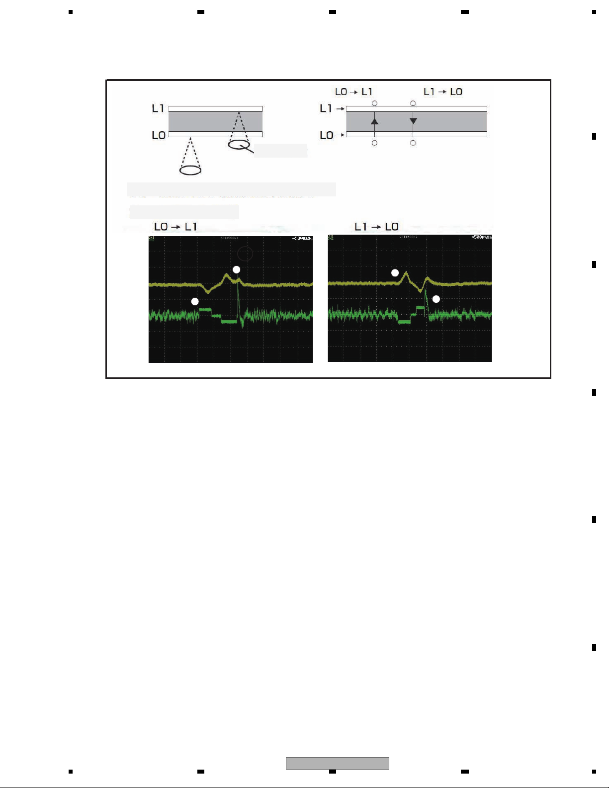
1.2.4 Focus jump
Focus jump is a function compatible to 2 layers on one side or 2 layers on both sides. Looking from the object lens,
the layer close to the lens is called “layer 0” (L0) and the layer away from the lens is called “layer 1” (L1).
1.3 Auto adjustment function
All circuit adjustments are automated in this system.
Details of each auto adjustment are explained below.
1.3.1 VIN7, VIN8, VIN9, VIN10 offset cancel
Each signal from VIN7,8, 9 and 10 output by PU is converted to a digital signal by the AD converter in the servo block.
Offset cancel is a function to cancel input offset of the AD converter at the time of power ON.
1.3.2 VCO gain adjustment (VARI adjustment)
It has a function to absorb variation of VCO gain among individual LSI by learning so that auto adjustment is made to
maintain the VCO gain at a certain level. VCO is locked against the reference frequency for learning.
And, a frequency control value (FCNT) is read, and VARI register is adjusted so that the read value becomes the
same as the target FCNT value.
1.3.3 FE normalization adjustment
FE signal level measured at the time of focus close is adjusted so that it will become 190LSB at the digital equalizer
input stage.
FE
FD
Object lens
The waveform of the focus jump is shown below.
Focus jump waveform
The flow of the focus jump is shown below.
1. The tracking is opened by the layer being played back.
2. A command is issued to execute jump to the target layer.
3. The tracking is closed at the layer after the jump and the playback is resumed.
Incidentally, the process when the jump command is issued is as described below.
1. The lens is accelerated to the target layer until the FE signal detects the focus jump acceleration end level.
Acceleration will be ended by force, however, if the time for acceleration timeout has elapsed before detecting the
acceleration end level.
2. The drive voltage is not output until the FE signal detects the speed reduction start level, and the lens is moved by
inertia.
3. The lens speed is reduced from detection of the speed reduction start level until detection of the speed reduction
end level. Speed reduction will be ended by force, however, if the time for speed reduction timeout has elapsed
before detecting the speed reduction end level.
B
A
C
D
CX-3250
9
Page 10
1234
1234
C
D
F
A
B
E
State
Power ON
F close
F close (after TBAL)
T close
Coefficient
VIN7 offset
VIN8 offset
VIN9 offset
VIN10 offset
FEPP(FEMAX-FEMIN)
AS MAX
FE normalization
TEPP(TEMAX-TEMIN)
TE normalization
F gain
T gain
AS normalization
DVD
05FB~0A17
05FB~0A17
-
1D84~6C08
No standard
No standard
2328~59D8
No standard
0100~0400
0100~0400
No standard
CD
0533~0B0C
0533~0B0C
2E18~A8CF
1E91~98D1
Note) Coefficient values are indicated in hexadecimals. In all cases, specifications
at the production line are described. For discs, TDV-582 is used for DVD and TCD-792 is used for CD.
1.4 CIRC block (MN2DS0018MAUB : IC1501)
The CIRC block includes the digital signal processing function (EFM modulation and error correction) of CD-DA and
CD-ROM and the digital servo processing function of the spindle motor.
1.5 DRC block (MN2DS0018MAUB : IC1501)
The digital read channel (DRC) is equipped with A/D converter, digital equalizer (DEQ), Adaptive filter, Viterbi
detector, digital PLL circuit, RISC interface and periphery circuits for reading of signal on optical disc.
The list of auto adjustment coefficient
1.3.4 Focus balance (FBAL) adjustment
The focus position is adjusted so that the RFENV will be the maximum at the time of focus close tracking open and
tracking close.
1.3.5 DPD amplitude adjustment
I perform the gain adjustment of the analog step so that the input signal of the DPD comparator of the TE generation
circuit of the DVD becomes constant.
1.3.6 Learning of tracking error amplitude
At the time of focus close and tracking open, the lens is oscillated in the track direction and adjusted so that the TE
amplitude level becomes 190 LSB at the digital equalizer input stage.
1.3.7 Tracking balance (TBAL) adjustment
At the time of focus close and tracking open, the lens is oscillated in the track direction and the balanced point where
the DC offset becomes zero is searched and adjusted by using the Newton-Raphson method.
1.3.8 OFTR adjustment
The binary threshold level is adjusted to make the OFTR signal into a binary digit.
1.3.9 AS normalization adjustment
The AS signal level is measured for the designated number of samples at the time of track closing, and after A/D
conversion at the ADSC, it is fine adjusted to become 64 LSB at the digital equalizer input stage.
1.3.10 Focus gain adjustment, tracking gain adjustment
At the time of tracking close, a disturbance is entered into the servo loop to adjust to the target gain intersection.
All auto adjustments can be confirmed by displaying the adjustment result in the test mode.
10
CX-3250
Page 11
5 678
56
7
8
C
D
F
A
B
E
1.6 LS1 Power Supply Map
VD8(Driver)
8 V+/-0.4 V
VD8(Reg)
8 V+/-0.4 V
VDD5
5 V+/-0.4 V
1chip Driver(8 V)
5 V Reg(VCC5)
5.0 V +/-0.1 V
IC1002
S-1133B50-U5
LD
Photo IC
5 V Reg(AVCC5)
5.0 V +/-0.1 V
IC1003
S-1200B50-M5
ADAC
IC1801
PCM1753DBQ
3.3 Reg(VCC33)
3.0 V<--->3.45 V
IC1004
NJM2885DL1-33
1.2 DC/DC(VCC12)
1.08 V<---> 1.32 V
IC1005
R1232D121B
DVD1chip(3.3 V)
SDRAM
IC1480
K4S641632N-LC75
Flash-ROM 1 (Program)
IC1402
S29AL016J70TFIC10H
Other
DVD1chip(1.2 V)
VD8V
HOST
Power Supply
Mecha inside
Power Supply
Pick Up Unit
CGY5000
1chip Driver
IC1201
BD8231EFV
DVD LSI
IC1501
MN2DS0018MAUB
Supply
IC
Flash-ROM 2 (Data)
IC1401
S29AL016J70TFIC10H
USB Circuit
IC1951
TC7SZU04FU
CX-3250
11
Page 12

1234
1234
C
D
F
A
B
E
1.7 LS1 Clock circuit
[Outline]
By connecting a 27 MHz crystal oscillator to DVD-LSI (IC1501), DACCLK for externally connected Audio-DAC
is formed and supplied by the clock generator inside the DVD-LSI in addition to the clock used inside the LSI.
IC1501
DVD-LSI
R1508
220ohm
MN2DS0018MAUB
156pin 155pin
OSCO OSCI
R1501
12 pF
R1503
1Moh
CSS1768
1200ohm
27 MHz
X1501
10 pF
C1512
C1510
[
USB_Clock outline]
DACCLK
33.868 8 MHz
or 36.864 MHz
IC1801
Audio-DAC
PCM1753DBQ
By connecting a 48 MHz crystal oscillator to DVD-LSI (IC1501), clock is formed and supplied by the clock
generator inside the DVD-LSI in addition to the clock used inside the USB circuit.
IC1501
DVD-LSI
MN2DS0018MAUB
50pin
USB_Clock
R1953
10 pF
C1951
4pin(OUT_Y)
R1952
1 Moh
X1950
CSS1760
680 ohm
48 MHz
IC951
TC7SZU04
2pin(IN_A)
m
FU
10 pF
C1952
12
CX-3250
Page 13

5 678
56
7
8
C
D
F
A
B
E
1.8 LS1 Audio circuit
[Analog audio signal]
[Digital audio signal]
Zo=820 ohm
AVCC5
Radio audio circuit
17 pin
(Lch)
A
udio GND
LS1 Mechanism module
Audio DAC
(PCM1753)
15 pin
(Rch)
14,16,18 pin
(AudioGND)
fc=88 kHz
MUTE
Circuit
AMUTE
8 pin
47 kohm or more
47 kohm or more
IC1801
820 ohm
R1804
C1804
R1803
C1803
C1802
C1801
4.7 uF
4.7 uF
R1802R1801
100 kohm
100 kohm
CN1901
[Outline]
1 Analog audio signal
Serial 3 line digital output + DACCLK (audio clock) output from DVD-LSI (IC1501) are converted to
analog audio signal by Audio-DAC (IC1801), and are output from HOST IF connector (CN1901).
Furthermore, analog MUTE signal is also output from DVD-LSI (IC1501) via HOST IF connector
(CN1901) simultaneously.
2 Digital audio signal (IEC60958/IEC61937)
Digital audio signal (IEC60958/IEC61937), output from DVD-LSI (IC1501), is output via Multi-ch/Ripping
IF connector (CN1901).
25pin
(IECOUT)
IC1501
DVD_LSI
152pin
CN1901
R1504
12 ohm
820 ohm
1 800 pF
1 800 pF
CX-3250
13
Page 14

1234
1234
C
D
F
A
B
E
1.9 LS1 Video circuit
[Outline]
Composite signal is output from DVD-LSI (IC1501), and output from HOST IF (CN1901).
LS1 Mechanism module
VCC33
LPF & 75 ohm Video
CN1901
(*1)
DVD LSI
(DV5U)
IC1501
100 ohm
200 ohm
Zo=300 ohm
19 pin(CVBS)
138pin:Comopsite
20 pin
14
CX-3250
Page 15

5 678
56
7
8
C
D
F
A
B
E
1.10 LS1 SDRAM I/F
SDRAM interface
*When viewed from DVD-LSI
Signal Name Bits I/O
MDQ[15:0] 16 I/O
MA[11:0] 12 O
BA[1:0] 2 O
NRAS 1 O
NCAS 1 O
NEW 1 O
NCS 1 O
DQM[0] 1 O
DQM[1] 1 O
MCK 1 O
MCKI 1 I
SDRAM specifications
Data bus width: 32 bit
Operating frequency: 121.5 MHz
CAS latency=3
8 word burst transfer
Manual precharge
CAS before RAS refresh (Auto refresh)
SDRAM connection configuration
DVD-LSI SDRAM
I
C1501 IC1480
MDQ[15:0] DQ[15:0]
MA[11:0] A[11:0]
BA[1:0] BA[1:0]
NRAS XRAS
NCAS XCAS
NEW XWE
DQM[1:0] DQM[1:0]
NCSM XCS
MCK CLK
MCKI
Description
Data bus of external SDRAM
SDRAM address
SDRAM bank address
RAS signal of SDRAM
CAS signal of SDRAM
Write enable signal of SDRAM
Chip select signal of SDRAM
SDRAM data mask 0
SDRAM data mask 1
Clock input to SDRAM
Clock input for data input from SDRAM
[Outline]
It is a memory for realizing the AV decoding function of DVD-LSI (IC1501). It is used for various purposes
such as buffering of stream data before decoding, working area for decoding, and storing of AV data or
output data after decoding.
CX-3250
15
Page 16

1234
1234
C
D
F
A
B
E
[Outline]
It inputs a D-/D+ signal into DVD - LSI (IC1501) than HOST IF (CN1901).
It uses CP_RESET, SDA, SCL by the iPod certification.
DVD LSI
(DV5U)
VCC33
CN1901
IC1501
R 1951
28pin(SDA)
29pin(RESET)
VCC33
VCC33
VCC33
1.11 LS1 USB(iPod)circuit
LS1 Mechanism module
6.8 kohm
10 kohm
R 1527
R 1535
61pin
(CP_Reset)
46pin
(I2C_SDA)
47pin
(I2C_SC)
144pin
(LOUT)
146pin
(ROUT)
24 ohm
R 1950
24 ohm
R1546
R 1955
15 kohm
6.8 kohm
R 1532
100 ohm
R 1544
180 ohm
R 1543
180 ohm
R 1954
27pin(SCL)
22pin(D-)
23pin(D+)
15 kohm
24pin(DGND)
16
CX-3250
Page 17

5 678
56
7
8
C
D
F
A
B
E
Construction
CRG motor
PU Unit
Spindle motor
Module PCB
Connector PCB
Damper
CRG mechanism
Upper/Under Frame
2. MECHANISM DESCRIPTIONS
CX-3250
17
Page 18

1234
1234
C
D
F
A
B
E
State of CRG mechanism
Clamper arm assy
SW armRoller arm assy
Disc guide assy
18
CX-3250
Page 19

5 678
56
7
8
C
D
F
A
B
E
Disc loading operation
1.When the disc is inserted, the SW arm L and R rotate and then SW1 turns ON from OFF.
By the SW1 turning ON from OFF, the load carriage motor starts and then the rubber roller rotates.
2.In the case for a 12cm disc, SW1 is turned OFF from ON by the SW arm being opened widely and then the
microcomputer determines that the disc is 12cm.
3.In the case for a 8cm disc, SW arm does not open widely, so SW1 is not turned OFF from ON but goes into the clamp
movement and then the microcomputer determines the disc to be 8cm.
(SW arms are jointed on both sides, and even if one side is pushed, the joint part is locked and the arms do not open
more than a fixed width. (SW1 is not turned OFF from ON.))
Load carriage motor
PU unit
Roller
SW arm L
SW3
SW2
SW1
DISC
SW arm R
CX-3250
19
Page 20

1234
1234
C
D
F
A
B
E
Disc centering mechanism
1. 8cm disk is centered with the guide pin and the centering pin.
2. 12cm disk passes under the guide pin and the centering pin, and is centered at the mechanism interior position.
Centering pin
Guide pin Guide pin
8cm disc
Guide pin
Centering pin
Centering pin12cm disc
20
CX-3250
Page 21

5 678
56
7
8
C
D
F
A
B
E
Clamp Operation Structure
1.Drive the detection arm at the position where 8 or 12 cm disc is centered on the spindle.
2.Detection arm matches the jumping rack with the rack drive gear.
3.The drive lever that was jointed with the jumping rack slides and then lowers the clamp arm (it clamps the disc.).
At the same time, it rotates the roller arm and separates the rubber roller from the disc.
Moreover,rotation of the roller arm releases the upper and lower mecha locks and completes the clamp operation.
4.After the completion of the clamp operation, the control by the cam above the drive lever is released and then the
switching lock arm rotates.
When the same arm rotates, the switching idler gear is separated from the rack drive gear and meets with the feed screw
drive gear and then the carriage operation is executed.
Detection arm
Switching idler arm
Clamp arm
1
Switching lock arm
Feed drive gear
Worm wheel
Feed screw gear
1
4
Switching idler gear
5
Rubber roller
Jumping rack
2
Drive lever
Rack drive gear
3
Ejecting Operation
1.It starts the ejecting operation in the reverse order of above procedures when the load carriage motor rotates in the
reverse direction and the pick up is sent to the inner periphery with the home SW ON or more.
2.Ejection is completed when SW1 goes OFF->ON->OFF for 12cm disc.
3.Ejection is completed when SW1 goes ON->ON->OFF for 8cm disc.
CX-3250
21
Page 22

1234
1234
C
D
F
A
B
E
3. DISASSEMBLY
1.Have a specified part.
Please note that holding the front part of the upper frame or the CRG mechanical part,
or inserting a foreign substance could cause deformation.
Handling OK
Handling NG
How to have it
22
CX-3250
Page 23

5 678
56
7
8
C
D
F
A
B
E
Connector (relay FFC)
Relay FFC
Fig. 1 Fig. 2
GND the brown line
4V to the gray line
Mecha Module_Bringing into the Clamp State with No Disc Loaded
1. Remove the relay FFC from the connector on the module PCB side (Fig. 1).
(Precaution) When it is difficult to apply 4V to the motor in procedure 2 below, remove the connector on the relay
PCB side, then remove the FFC, and remove the solder of the CRG motor lead and apply voltage to the lead.
2. Push the Disc detection arm while applying 4V to the CRG motor (Fig. 2)
By this action, the mecha moves to the clamp state and the PU moves to the outer periphery.
3. Stop the motor when the PU comes to the vicinity of the intermediate periphery.
(Precaution) If the PU goes to the outer most periphery, it idles.
It is not a problem, but please try not to let it idle as much as possible.
CX-3250
23
Page 24

1234
1234
C
D
F
A
B
E
T-case washer
Drive gear
Fig. 1
Fig. 2
b.Open-lock state
c.Clamp state with no disc loaded
CRG Mecha_Bringing into the Clamp State with No Disc Loaded
1.Remove the CRG mecha assy according to the “Removing the CRG Mecha assy” manual
(mecha is in the ejecting state).
2.Remove the T-case washer and then remove the drive gear. (Fig. 1)
3.Lift the clamp arm assy until it is in the state shown in Fig. 2_b (open-lock state).
4.Put your finger on the area A of Fig. 2_c and then slide it to the direction of the arrow (the direction of the playing state).
5.Push down the clamp arm.
(Precaution) When bringing the CRG mecha into the ejecting state again, install the drive gear after sliding the drive lever
and bringing it to the ejecting state, in order to prevent the cog of the pinion in the drive gear from chipping at the time of
its installation.
a.Ejecting state
There is a
space
There is
no space
A
24
CX-3250
Page 25

5 678
56
7
8
C
D
F
A
B
E
Connector (pick up FPC)
Connector(Relay FFC)
PCB clinch screw
Short-circuit
Fig.1
Fig. 2
Fig.3
Pick up FPC
Relay FFC
Fig. 4
Solder on the lead
Relay PCB clinch screw
Hook A
Hook B
Fig. 5
Hook B
Fig. 6
Fig. 7
Fig. 8
Removing the Module PCB
1.Short-circuit two spots on the land of the pick up FPC. (Fig. 1)
2.Remove the pick up FPC and the relay FFC from the connector. (Fig. 2)
3.Temporarily attach the pick up FPC to the pick up rack. (Fig. 3)
(in order to prevent the damage to the pick up FPC)
4.Remove the two PCB clinch screws and then remove the module PCB. (Fig. 2)
Removing/Installing the Relay PCB
Removing)
1.Remove the relay FFC from the connector
(remove both sides so that the entire FFC will be removed). (Fig. 2)
2.Remove the solder on the lead for the CRG motor. (Fig. 4)
3.Remove the one relay PCB clinch screw. (Fig. 4)
4.Slide the relay PCB to the direction of the arrow and then remove
the relay PCB from the hook A and the hook B. (Fig. 4)
5.Turn the relay PCB over and then remove the SPDL motor FFC
from the connector.
Installing)
1.Check the mecha is in the ejecting state (disc-load suspended state).
When it is not in the ejecting state, apply 4V to the lead (motor) and
then bring it to the ejecting state (4V to the brown line and GND the gray line).
2.Fit the SPDL motor FFC to the connector (back of the relay PCB).
3.Hold the relay PCB so that it does not touch the SW knob as in Fig. 5.
4.Insert it into the hook B as it is a little off to the clockwise direction.
(Precaution) This is to prevent the SW knob from getting into the NG
position as in Fig. 6.
5.Push down the relay PCB lightly and then rotate it to the
counterclockwise direction.
It sets the relay PCB in the hook A and the positioning dowel.
(Precaution) Pay attention so the SW knob will not get onto the PU rack.
(Fig. 6)
6.As in the Figures, while supporting the location A with your fingers,
screw the relay PCB. (Fig. 7 / Fig. 8)
7.Solder the lead for the CRG motor.
8.Fit the relay FFC to the connector.
NGOK
A
CX-3250
25
Page 26

1234
1234
C
D
F
A
B
E
Fig. 2a
Permanently hooked position
Temporary hooked position
Fig. 2b
Slide to the direction of inner periphery
Fig. 1
Fig. 3
Fig.4
Regularly installed position
Install avoiding the
area with blue broken
line (the connected
metal plate part)
The spring is installed under the resin flange and inside
the bended metal plate.
Outside holder
Back end of
the feed screw
Removing the PU Unit
1.Bring to the clamp state with no disc loaded according to the “Bringing into the Clamp State with No Disc Loaded
(Motor Drive)” manual.
2.Remove the module PCB according to the “Removing the Module PCB” manual.
3.Hook the feed screw biasing spring on the temporary hook (Fig. 2b). Be careful not to get injured by the tip of the spring.
4.Hold the PU at the location A in Fig. 1 and slide and scoot it to the direction of the inner periphery.
5.As in Fig. 3, shift the back end of the feed screw to the side and then to above and remove it from the outside holder.
6.Remove the tucking joint for the chassis at the location B and the PU unit by lifting them up without changing their
position and then remove the PU unit.
(Precaution) When installing the PU again, make sure to tuck the chassis in B and the PU unit (Fig. 4) first.
Moreover, do not forget to permanently hook the feed screw biasing spring (Fig. 2a).
Adjustments to the PU after its installation should be made according to the service manual.
Sending the PU to the outer periphery
1.Bring to the clamp state with no disc loaded according to the “Mecha Module_Bringing into the Clamp State with
No Disc Loaded” manual.
(Precaution) The relay FFC must be removed for certainty in order to prevent the IC damage.
2.Apply 1.5V to the CRG motor and then transfer the PU to the outer periphery.
(Precaution) Do not forget to reinstall the relay FFC after sending the PU to the outer periphery and take the
necessary measures.
[Installation NG]
The chassis is not tucked
between the PU case and the
PU rack.
A
B
26
CX-3250
Page 27

5 678
56
7
8
C
D
F
A
B
E
Spindle motor
Spindle motor clinch screws
Removing the Spindle Motor
1.Remove the CRG mecha assy according to the “Removing the CRG Mecha assy” manual
(mecha is in the ejecting state).
2.Bring to the clamp state with no disc loaded according to the “Bringing into the Clamp State with No Disc Loaded
(Manual)” manual.
3.Remove the clamp arm according to the procedure 3 and after of the “Removing the Clamp Arm” manual.
4.Remove the relay PCB according to the “Removing the Relay PCB” manual.
5.Remove the two spindle motor clinch screws and then remove the spindle motor assy.
CX-3250
27
Page 28

1234
1234
C
D
F
A
B
E
Removing the Clinch of the Bottom Frame
1.Use the needle-nose pliers when removing the clinch on the right side.
Nip the clinch at the location in Fig. 1a and then open it until it is in the position
circled by the red broken line in Fig. 2a.
2.Also to remove the clinch on the left side, use the needle-nose pliers,
nip the clinch at the location in Fig. 1b and then open it until it is in the position
circled by the red broken line in Fig. 2b.
(Precaution) When clinching again, use Fig. 2a and Fig. 2b as a guide.
It is okay as long as the tip of the clinch does not come off from the side a and
the side b by the vibration stroke (from front to back and from side to side).
Check Fig. 3a and Fig. 3b for the height of the clinch.
Correct the height with the needle-nose pliers when the height does not meet
the standard listed in those Figures.
In case of metal fatigue on the clinch part, exchange the lower frame.
Caution: After repairing, make sure to clinch to the lower frame again.
Fig. 1a
Fig. 1b
L
It is bended orthogonally
in the initial condition
Clinch on the left side
It is in the L/2 position
in the initial condition
Clinch on the right side
Fig. 2a
Fig. 3a
28.9+0.6/-0.3
(28.6 - 29.5)
Fig. 2b
Fig. 3b
25.45+0.6/-0.3
(25.15 - 26.05)
28
CX-3250
Page 29

5 678
56
7
8
C
D
F
A
B
E
OK:The end of the groove of the shaft
is hidden by the damper exterior.
NG:The end of the groove of the shaft
is found outside the damper exterior.
OK:A shaft is found
inside the spring.
NG:A shaft is found
outside the spring.
Removing the CRG Mecha assy
1.Follow up to the procedure 3 of the “Removing the Module PCB” manual and then remove the PU FPC from the
connector.
2.Remove the relay FFC from the connector (both ends) and then remove the FFC. (Fig. 1)
3.Open the clinch of the bottom frame according to the “Removing the Clinch of the Bottom Frame” manual.
4.Remove the front-pulling springs on both sides. (Fig. 2a & Fig. 2b)
5.Remove four clinch screws of the top frame and then remove the top frame. (Fig. 3)
6.As lifting the carriage mecha, remove it from the dampers at three locations. (Fig. 3)
(Precaution) When assembling the CRG mecha assy again, apply alcohol on the dampers.
Make sure that the damper shafts are inside the three neutral springs (Fig. 4) and that the springs on both sides are hooked.
Before connecting to the module PCB after installing the CRG mecha, bring to the clamp state with no disc loaded
according to the “Mecha Module_Bringing into the Clamp State with No Disc Loaded” manual, push the upper part of the
damper of the CRG mecha by the finger and then make sure that the damper and the CRG mecha are jointed with certainty.
(Fig. 5)
Fig. 1
Fig. 4
Caution : After repairing, make sure to clinch to the lower frame again.
Caution : After repairing, make sure to clinch to the lower frame again.
Clinch screw of the top frame
Front-pulling spring
Fig. 2a
Fig. 3
Dampers
Front-pulling spring
Fig. 2b
Fig. 5
CX-3250
29
Page 30

1234
1234
C
D
F
A
B
E
Guide bracket clinch screw
Roller transmission side gears
Fig. 1
Fig. 2
Roller assy biasing spring
Fig. 3
Disc guide assy
Roller Guide assy
Fig. 4
Removing the Disc Guide assy
(Removing the Roller Transmission Side Gear)
1.Remove the CRG mecha assy according to the “Removing the CRG Mecha assy” manual (mecha is in the ejecting state).
2.Remove the two guide bracket clinch screws and then remove the Disc guide assy. (Fig. 1)
3.Remove the two roller transmission side gears. (Fig. 2)
(Precaution) When assembling the Disc guide assy again, do not forget to install two gears on the side panel.
Removing the Roller assy
1.Remove the CRG mecha assy according to the “Removing the CRG Mecha assy” manual (mecha is in the ejecting state).
3.Remove the Roller assy biasing spring. (Fig. 3)
4.Remove the Disc guide assy according to the procedure 2 and after of the “Removing the Disc Guide assy” manual.
5.Hold the Roller assy at the locations A, slide it to the left and then remove it. (Fig.4)
(Precaution) When assembling the Disc guide assy again, do not forget to install two gears on the side panel.
A
30
CX-3250
Page 31

5 678
56
7
8
C
D
F
A
B
E
Removing/Reassembling the Clamp Arm assy
1.Remove the CRG mecha assy according to the “Removing the CRG Mecha assy” manual
(mecha is in the ejecting state).
2.Bring to the clamp state with no disc loaded according to the “Bringing into the Clamp State with No Disc Loaded
(Manual)” manual.
3.Remove the right clamp arm biasing spring. (Just on the clamp-arm side. Do not remove on the chassis side.)
4.Lift the clamp arm assy until it is in the state shown in Fig. 2 (open-lock state).
5. Lightly push the part A and lift the clamp arm assy further to the position in Fig. 3.
6. Remove the left clamp arm biasing spring.
7. Lift the clamp arm assy further to 45-60 degrees, slide it to the left and then remove it. (Fig. 1)
Fig. 2
Fig. 3
Fig. 1
Left biasing spring
A
Right biasing spring
Poly slider
Installing)
1.With the clamp arm assy tilted at 45-60 degrees, install it to the rotation fulcrum by sliding it from the left.
2.Bring down the clamp arm assy to the position in Fig. 3 (position where it meets the chassis and then stops).
3.Install the left clamp arm biasing spring.
4.Completely turn the detection arm to the position OK in Fig. 4 and then push the clamp arm assy to the bottom.
5.Install the right clamp arm biasing spring.
(Precaution) –When replacing the clamp arm assy, replace the poly slider with a new part as well.
Do not forget to apply the E paste on the poly slider (Fig. 4).
Fig. 3
Fig. 4
NGOK
Apply the E paste on the yellow area.
Clamper convexity contact zone
CX-3250
31
Page 32

1234
1234
C
D
F
A
B
E
Fig. 1
Remove the solder
Line clamper
Slide the spring
to remove it
CRG motor biasing spring
Fig. 2a
Fig. 2b
Correctly installed condition
Joint removed condition
Fig. 4
Switching idler arm (Pull upward)
Fig. 3
Idler gear
Worm wheel
Switching idler arm biasing spring
CRG motor clinch screw
Fig. 5
Remove the joint
hook
Fig. 6a
Fig. 6c
Fig. 6b
A
Removing the CRG Motor assy
(Removing the Drive Transmission Gear)
1.Remove the CRG mecha assy according to the “Removing the CRG Mecha assy” manual (mecha is in the ejecting state).
2.Remove the clamp arm assy according to the “Removing the Clamp Arm assy” manual.
3.Remove the solder of the CRG motor lead and then remove the lead from the line clamper. (Fig. 1)
4.Remove the clinch screw of the CRG motor biasing spring and then slide the biasing spring to the direction of the arrow to remove it. (Fig. 1)
5.Nip the gear hook of the switching idler arm by the tips of your fingers and then push it below from the top of the gear. (Fig. 2a -> Fig. 2b)
6.Bend the hook on the chassis side of the switching idler arm to the direction of the arrow by tweezers and then remove the joint with the chassis.
(Fig. 3)
7.Pull off the switching idler arm from the top of the mecha (Fig. 4) and then remove the worm wheel and the idler gear. (Fig. 3)
8.Remove the switching idler lock arm biasing spring. (Fig. 3)
9.Remove two CRG motor clinch screws and then remove the CRG motor. (Fig. 3)
(Precaution) When installing the switching idler arm again, temporarily set the idler gear and the worm wheel as in Fig. 5, press the idler gear
from its top by your finger and then install the switching idler arm according to the steps in Fig. 6 from the opposite side of the chassis.
Do not forget to install the switching idler arm biasing spring.
Since the idler arm is in the snap fit structure, do not use them again.
When installing the CRG motor, scoot it to the center of the mecha in order to ensure that the gear engages.
Step 1: Insert the arm rotation fulcrum boss in the worm
wheel through the chassis hole.
Insert only the tip of the boss as in the figure.
Step 2: As pressing the idler gear from the opposite,
insert the gear fulcrum boss into the gear and joint them
until they are in the correctly installed condition in Fig. 2a.
When the idler arm is not installed correctly, there could be
an interference either in the location a or in the location b of
Fig. 4. Make a fine adjustment by moving it left and right.
Step 3: As matching the tip of the rotation fulcrum boss
with the metal plate hole by your finger (Fig. 6b), push the
area A in Fig. 6c to install the idler arm.
a: Match the fulcrum hole of the worm wheel
with the metal plate hole.
b: Engage the idler gear with the worm wheel.
c: Align the gear with the outer shape of the metal plate concavity as a guide.
Biasing spring cylind screw
Switching idler arm
a
b
c
32
CX-3250
Page 33

5 678
56
7
8
C
D
F
A
B
E
Fig.5
Part C : NG
Position with
inadequate
approach
Part C : OK
Position with
adequate
approach
Idler gear
Removing the Drive Lever assy
1.Remove the CRG mecha assy according to the “Removing the CRG Mecha assy” manual (mecha is in the ejecting state).
2.Remove the clamp arm assy according to the “Removing the Clamp Arm assy” manual.
3.Remove the drive lever biasing spring. (Fig. 1)
4.Slide the drive lever to the direction of the arrow (the direction of ejecting), lift it to the direction of upper right and then
remove it. (Fig. 2)
(Precaution) When installing the drive lever assy again, install the part B (Fig. 2) first with the part A in Fig. 3 scooted to
the direction of the arrow(*1). Next, install the part C (Fig. 4) of the drive lever in the channel bending the side of the
chassis, and in the end, install the part D (Fig. 4) into the L-shaped channel of the chassis and then slide the drive lever to
the position in Fig. 1.
Fig. 3
*1: If approach of Part A (Fig 3) is inadequate, the drive lever will not be
able to be well incorporated.
In this case, the idler gear might be located at the red dashed line (Fig 5).
Therefore, approach Part A (Fig 3) to the direction of the arrow as
approaching the idler gear to the direction of the arrow (Fig 5).
Determine, with the position of Part C in Fig 5, if the approach of
Part A is adequate.
Drive lever biasing spring
Fig. 1 Fig. 2
A
Fig. 4
D
B
C
CX-3250
33
Page 34

1234
1234
C
D
F
A
B
E
Connecting lever biasing spring
Fig. 1
Fig. 2
Removing the SW Arm
1.Remove the roller arm assy according to the “Removing the Roller Arm assy” manual.
2.Remove the SW arm connecting lever biasing spring. (Fig. 1)
3.Open the SW arms on both left and right sides until their tips touch the chassis. (Fig. 2)
4.Keep the SW arms open, lift them upward and then remove them.
Removing the Damper
1.Remove the CRG mecha according to the “Removing the CRG Mecha assy” manual
2.Insert the screwdriver under the part A of the metal plate configuration which joints the damper, lift the metal plate to
release the damper from being clinched by the part C.
3.Insert the screwdriver under the part D as well. Lift the metal plate, release the damper from being clinched to remove it.
A
C
D
Open the SW arms on both left and right side
Open the SW arm
on left sides until their tips
Open the SW arm
on right sides until their tips
Caution: After repairing, make sure to clinch to the lower frame again.
Caution: When mounting a damper, hold it tight with a clinch in order to avoid backlash.
In case of metal fatigue on the clinch part, exchange the frame.
34
CX-3250
Page 35

5 678
56
7
8
C
D
F
A
B
E
Fig. 7
Fig. 2
Hook
PU rack
Fig. 1
PU rack clinch screw
Fig. 3
Fig. 6
Fig. 4
FFC folding line
FFC folding back part
C
Fig. 8
Actuator
Removing the PU Rack
1.Remove the PU unit according to the “Removing the PU Unit” manual.
2.Remove the PU rack clinch screw. (Fig. 1)
3.Pick up the root of the hook on the PU rack (Fig. 2) with tweezers as in Fig. 3. While bending it so the tip of the hook
would open to the direction of the arrow (unhooked direction), pull out the PU rack upward.
(Precaution) When handling the PU unit, do not “touch the actuator in Fig. 9 or hit the desk with it during the operation.”
Handle the PU and the PU unit according to “Holding the PU” manual.
When installing the PU rack into the PU again, fold back the PU FPC as in Fig. 5 according to the folding line in Fig. 4
before installing the rack and settle it in the channel on the PU case. To install the PU rack, first install the part a and the
part b in Fig. 6 into the PU case, install the FPC folding back part in Fig. 5 so that it is held by the part A in Fig. 7, and push
the part B (top of the snap fit) to fit the PU rack.
When it is hard to fit the PU rack, try again as scooting it to the direction of the arrow C in Fig. 7.
After installing the PU rack, insert the feed screw from the side c in Fig. 8. Insert approximately 18mm on the part shown in
the figure.
Fig. 5
A
B
Fig. 7b
OK
NG
Fig. 9
CX-3250
35
Page 36

1234
1234
C
D
F
A
B
E
Handling OK
Handling NG
Do not touch the object lens.
Do not touch the ACT.
Do not touch the Hologram.
Do not pull the FPC.
Holding the PU
1.Hold the “Handling OK” area of the PU indicated by the figure. Do not hold the “Handling NG” area.
36
CX-3250
 Loading...