

Page 1

ORDER NO.
CRT3896
DVD MECHANISM MODULE(MS5)
CX-3212
- This service manual describes the operation of the DVD mechanism module incorporated in models
listed in the table below.
- When performing repairs use this manual together with the specific manual for model under repair.
Model Service manual DVD Mechanism Module
AVIC-D3/XU/UC CRT3879 CXK6601
AVI C- D3/XU /EW5
CONTENTS
1. CIRCUIT DESCRIPTIONS................................................................................................................................2
2. MECHANISM DESCRIPTIONS ......................................................................................................................19
3. DISASSEMBLY ...............................................................................................................................................24
PIONEER CORPORATION 4-1, Meguro 1-chome, Meguro-ku, Tokyo 153-8654, Japan
PIONEER ELECTRONICS (USA) INC. P.O. Box 1760, Long Beach, CA 90801-1760, U.S.A.
PIONEER EUROPE NV Haven 1087, Keetberglaan 1, 9120 Melsele, Belgium
PIONEER ELECTRONICS ASIACENTRE PTE. LTD. 253 Alexandra Road, #04-01, Singapore 159936
PIONEER CORPORATION 2007
K-ZZU. FEB. 2007 Printed in Japan
Page 2

1234
1. CIRCUIT DESCRIPTIONS
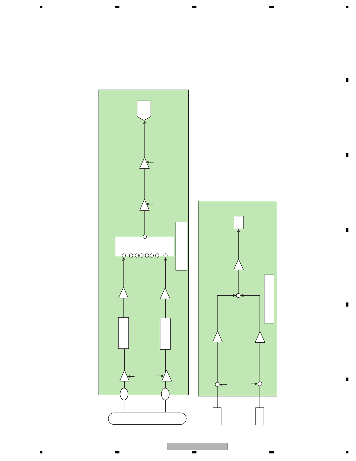
1. Front end section (MN2DS0016AAUB : IC1501)
MN2DS0016AAUB is a 1 chip LSI for DVD-Player. A DVD-Player system can be constructed by connecting this LSI,
A
driver IC, SDRAM, Flash-ROM, Audio-DAC, etc.
This LSI includes a front end (SODC/FE) which executes RF signal processing, servo processing and decode
processing, a back end (AV decoder/BE) which executes video decode processing such as MPEG1/MPEG2/JPEG
and audio decode processing such as DVD-Audio/Dolby Digital /DTS/MP3, and a system controller which controls
the system.
The front end section realizes optical head signal computation processing and RF signal processing, digital signal
processing (16-8 demodulation, error correction) for DVD-ROM playback according to the DVD specifications,
digital signal processing of CD-DA/CD-ROM (error correction), AV decoder transfer, servo control, spindle motor control
and seek control.
In the case of MN2DS0016AAUB, the front end servo system waveforms, such as FE, TE and AS, are not observed
as in the case of DVD mechanism module (MS4) CX-3183. Please pay attention.
B
1.1 Analog block (MN2DS0016AAUB : IC1501)
The functions of the analog block are as described below.
1. Reference power circuit
2. SERVO system/DPD system signal processing circuit
Gain switching amplifier and Low Pass Filter (LPF)
3. RF signal processing circuit
RF adding circuit, circuit to make inline, Variable Gain Amplifier (VGA) circuit
4. Laser power control (LPC) circuit
5. A/D converter for SERVO (10 bit, DPD system-4ch), PWM
2
1.1.1 APC circuit
C
The optical output of the laser diode (LD) has a large negative temperature characteristic.
Therefore, if the LD is driven by a constant current, a constant optical output cannot be obtained.
APC circuit is a circuit to control the current so that the output at the monitor diode (MD) will be constant.
MN2DS0016AAUB includes 2 types of APC circuit, one for DVD and the other for CD.
The LD current can be obtained by dividing the measured voltage between DVDLD1 (CDLD1) and 5 V by 6 Ω
(1.5 Ω x 4=6 Ω), in the case of DVD (CD). It will be approximately 50 mA (45 mA) in the case of DVD (CD).
The potential difference between DVDLD1(CDLD1) and 5 V is set to approx. 300 mV(270 mV).
D
CDMPD
14
DVN Chip
E
(MN2DS0016AAUB : IC1501)
DVDMPD
F
2
1234
CX-3212
PU UNIT
Page 3
5 678
A
ADC
ADC driving AMP
Buffer AMP
Selector
ADC
Selector
Gain switching
6/7.5/9/10.5/
12/13.5/15/
16.5/17/19.5 dB
Gain switching
3 dB, 9 dB
DVN Chip
AMP
B
C
FE
D
Gain switching
12
G=0 dB
LPF
50 k/100 kHz
-6 dB, 0 dB, 9.5 dB
VIN5
136
11
FE1
Buffer
LPF
LPF
50 k/100 kHz
Input AMP
VIN6
137
FE = (FE1) - (FE2)
The signal from PU, FE1 and FE2, are AD converted inside IC1501 and captured. After that, a differential is obtained by taking the offset cancellation into consideration,
1.1.2 FE forming circuit
and FE is obtained.
Focus error (FE) forming circuit
56
CN1101
FE2
FE signal forming circuit
1+Pfbal0,1/0x0100
After 10 bit ADC
CX-3212
FE1
+
-
DVN Chip
1-Pfbal0,1/0x0100
Fbal coarse adjustment value
Offset cancel
FE2
7
E
F
8
3
Page 4
1234
AMP
ADC2
TE
D
+
+
Phase
comparator
ADC3
ADC4
A
TE signal forming circuit
B
LPF (integrator)
Phase comparator
C
ADC
ADC1
AMP
G=-1 dB
/5.7 MHz
HPF
100 kHz
LPF
/5.7 MHz
27 M/11.3 M
VIN3RF
121
HPF
LPF
27 M/11.3 M
VIN4RF
120
HPF
D
Buffer
E
Input AMP LPF
HPF
100 kHz
Gain switching
G=0,3,6,9,12,15 dB
LPF
/5.7 MHz
27 M/11.3 M
Gain switching
–7.5 dB, 0 dB, 3.5 dB
VIN1RF
123
HPF
100 kHz
LPF
27 M/11.3 M
VIN2RF
122
DVN Chip
100 kHz
/5.7 MHz
0.1 μF
F
CN1101
1.1.3 TE forming circuit
Tracking error (TE) forming circuit
In the case of a DVD, the phase difference method is used for TE forming, and the TE is formed from the phase difference among (A+C) and (B+D).
In the case of a CD, 3 beam method is used, and after entering the signal into a variable amplifier for tracking offset adjustment via an external resistor, it is AD converted,
4
1234
and a TE is formed by the equation of TE=(E+G_E+F)-(F+H_G+H).
DVD (phase difference TE)
8
A
7
B
CX-3212
0.1 μF
0.1 μF
9
C
0.1 μF
10
D
Page 5
5 678
A
B
ADCSelector
AMP
Buffer AMP
Buffer
LPF
LPF
Selector ADC
G=0 dB
50 k/100 kHz
Gain switching
6/7.5/9/10.5/
12/13.5/15/
16.5/17/19.5 dB
Gain switching
3 dB, 9 dB
DVN Chip
LPF
50 k/100 kHz
TE
AMP
+
TE signal forming circuit
1+Ptbal0,1/0x0100
-
1-Ptbal0,1/0x0100
C
D
DVN Chip
E
Input AMP
CD (3 beam TE)
CN1101
56
VIN9
135
21
H
F+H_G+
Gain switching
-6 dB, 0 dB, 9.5 dB
VIN10
134
22
E+G_E+F
After 10 bit ADC
CX-3212
Offset cancel Tbal adjustment value
E+G_E+F
F+H_G +H
7
8
F
5
Page 6

1234
1.2 Servo block (MN2DS0016AAUB : IC1501)
A
At the servo block, focusing, tracking, servo control of traverse, spindle motor control and seek control are performed.
1.2.1 Focus close
Close to disc.
Lens
B
Merging
point
Late
C
After issuing the focus close command, both the DVD and the CD will perform the following processing.
1. Measurement and optimization of the signal level.
D
First the PU lens is driven in the direction getting away from the disc, then it is driven in the direction getting close
to the disc. At this time, each signal level of FE, AS and RFENV are measured at the focused focal point that the
lens passes, and the levels of FE and AS are optimized. (1 and 2 in the figure)
2. Focus adjustment
Next, after detecting the drawing level of FE and AS by driving the lens away from the disc, the focus loop filter is
activated and the focus is drawn. (3~6)
3. Confirmation of adjustment
Confirm the drawing at the signal level of AS and RFENV. (6, 7)
The signal levels of FE, AS and RFENV and the focus drive voltage can be checked by the focus search in the
test mode.
E
1.2.2 Tracking close
After issuing the tracking close command, both the DVD and the CD will perform the following processing.
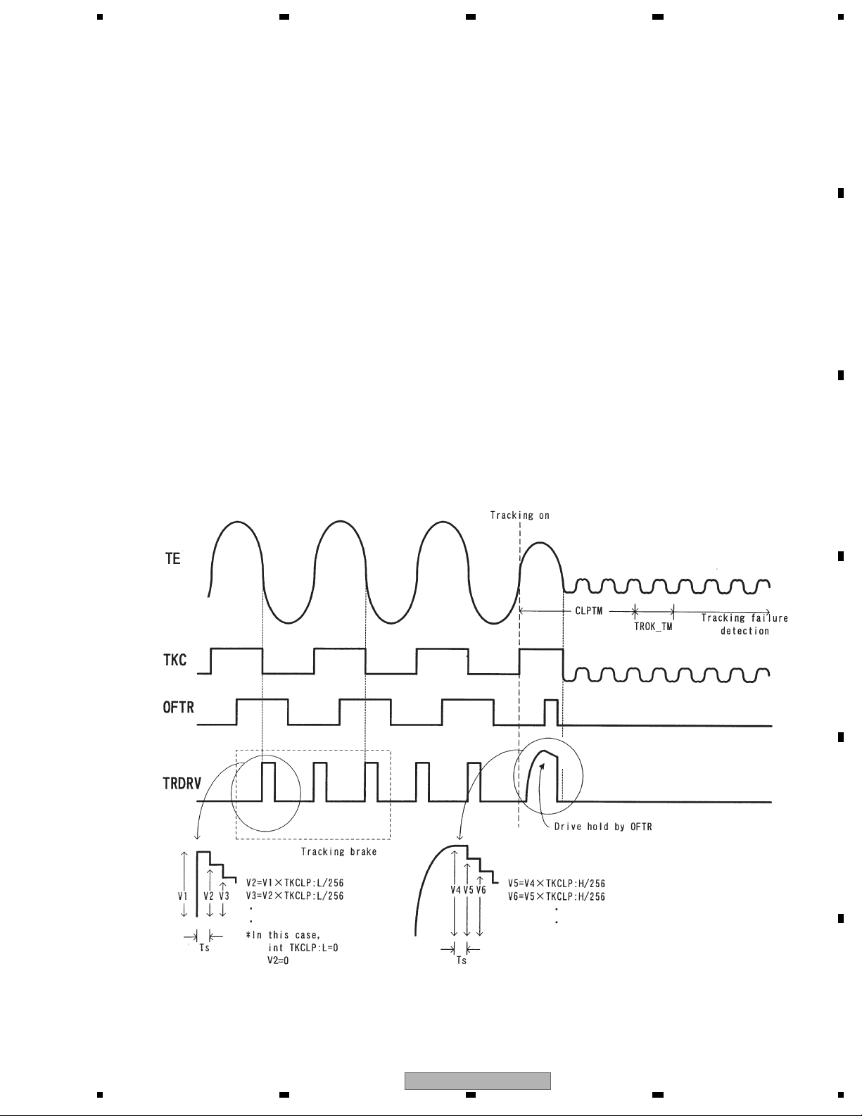
1. Tracking brake
1/2 cycle of the track cross is measured and if the cycle is within the specified range, the brake pulse is output.
The output direction of the brake pulse is determined by the phase relationship of the OFTR and the TKC
(binary signal of TE) signals. When it is confirmed that the swinging of the lens against the disc has been controlled,
braking will be stopped and enters into drawing. If the drawing conditions are not met within 10 msec, after the brake
output, the brake will be ended and entered into drawing.
2. Tracking adjustment
Tracking drive hold processing by the OFTR signal will be performed.
3. Confirmation of adjustment
F
Checking is made that the number of track jumps within the specified period of time are at the designated numbers
or less. The time out for confirmation of adjustment is 8.4 msec. and retry is performed by the command from the
microcomputer.
6
1234
CX-3212
Page 7
5 678
1.2.3 Track jump
In this system, one of the three methods, interval jump, multi jump or traverse seek, is selected depending on the
number of target moving tracks.
1. Interval jump
Detailed seek can be performed to execute repeated track jump of 1 track, and it is used when the target track gets
close or at the time of seek operation to the adjacent track.
2. Multi jump
Both edges of the track cross signal TKC are counted, and track count move of the designated number is executed.
Furthermore, the stepping motor is driven according to the number of jumps.
3. Traverse seek
The stepping motor is controlled by F/W. Track count by TKC is not performed, and the stepping motor is moved
according to the number of jumps. In the case of a DVD, seek is performed by maintaining the pick up at the mid
point using the mid point servo by the microcomputer.
It indicates the setting for jump switching common to DVD and CD.
Types of target move number of jumps.
DVD
~10 Interval jump
1
~500 Multi jump
11
~878 Combination of multi jump and interval jump
501
~1756 Traverse seek (short)
879
~ Traverse seek (long)
1757
CD
~10 Interval jump
1
~400 Multi jump
11
~780 Combination of multi jump and interval jump
401
~928 Traverse seek (short)
781
~ Traverse seek (long)
929
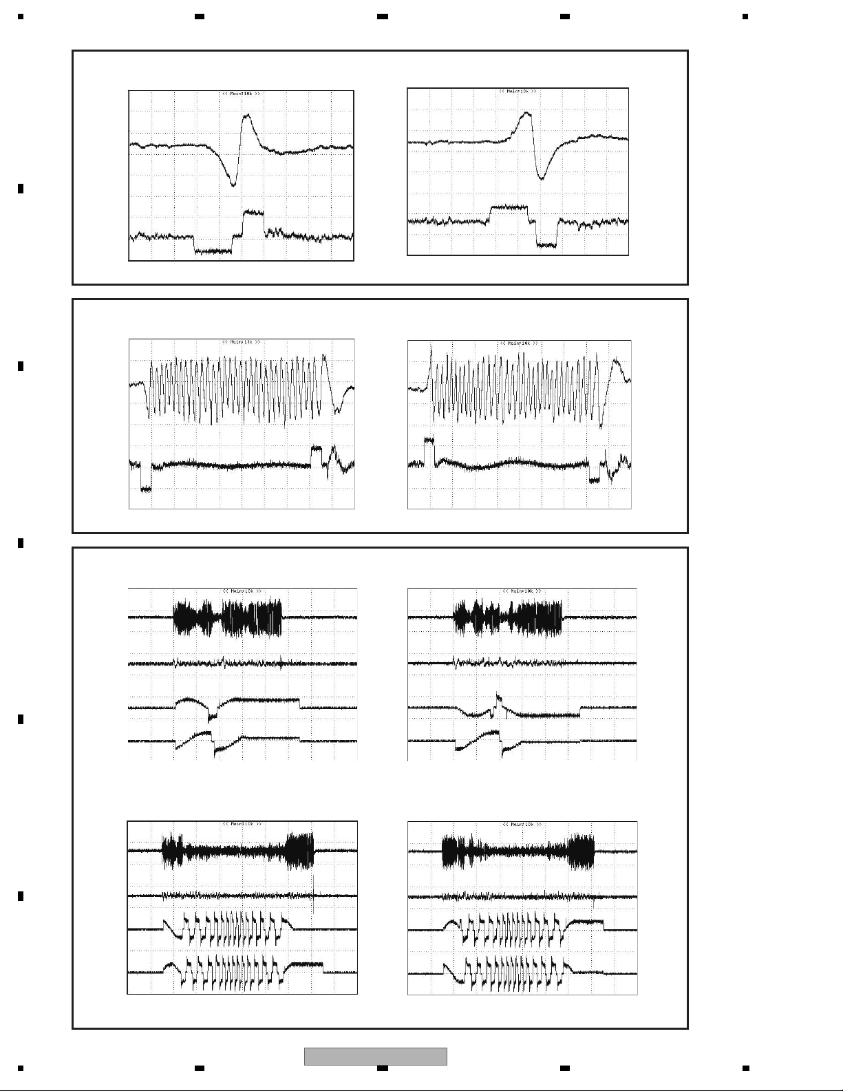
The waveform of track jump is shown on the next page.
Tracking-on process
A
B
C
D
E
F
CX-3212
56
7
8
7
Page 8
1234
Interval jump (1 track) DVD
Outer peripheral jump Inner peripheral jump
A
TE
TD
B
Multi jump (32 track) DVD
Outer peripheral jump Inner peripheral jump
TE
C
TD
Traverse seek (900 tracks)
A ± and B ± are measured by setting the LPF of the oscilloscope to 10 kHz.
Outer peripheral jump Inner peripheral jump
D
TE
TD
A±
B±
Traverse seek (10 000 tracks)
E
Outer peripheral jump
Inner peripheral jump
TE
TD
A±
B±
F
8
1234
CX-3212
Page 9
5 678
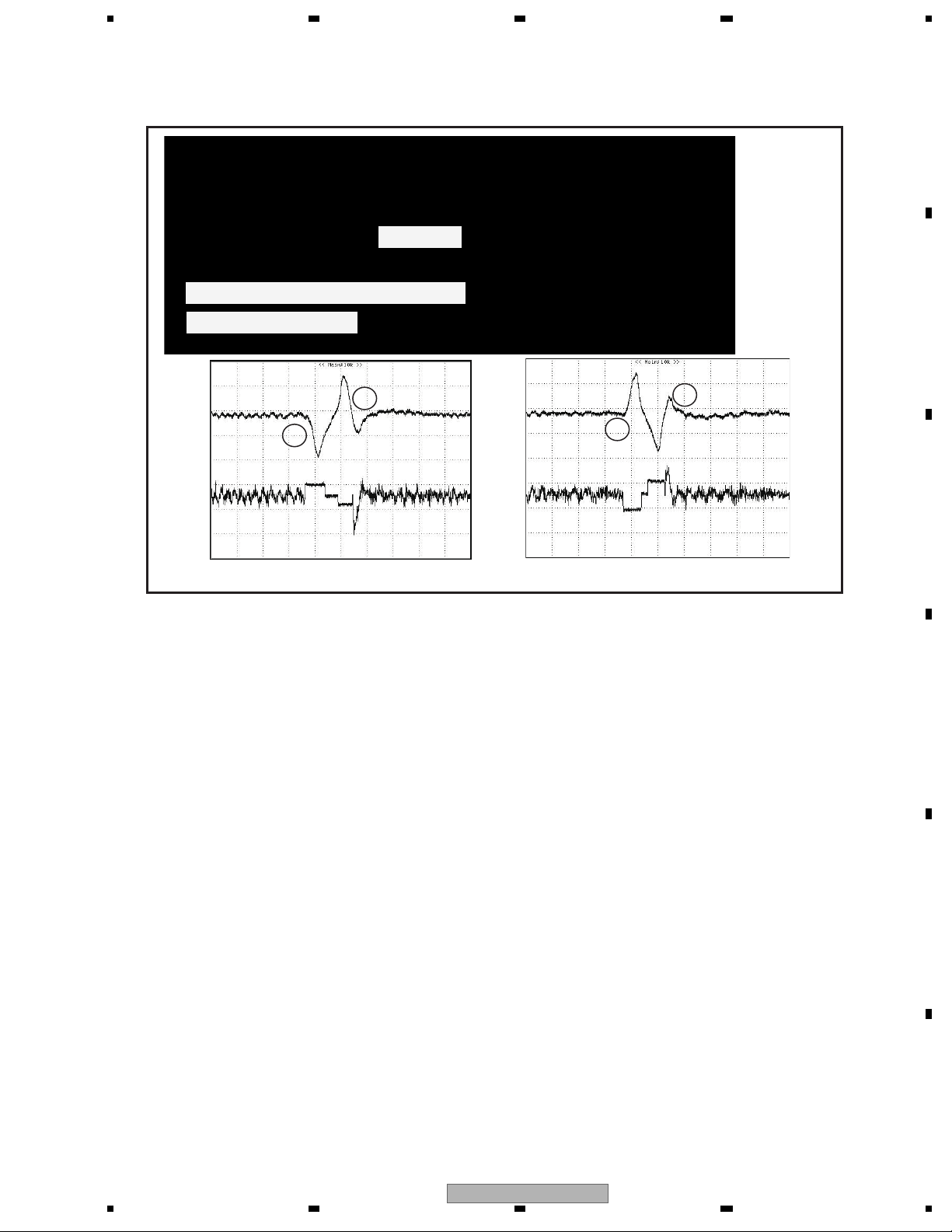
1.2.4 Focus jump
Focus jump is a function compatible to 2 layers on one side or 2 layers on both sides. Looking from the object lens,
the layer close to the lens is called “layer 0” (L0) and the layer away from the lens is called “layer 1” (L1).
Object lens
The waveform of the focus jump is shown below.
Focus jump waveform
A
B
B
D
FE
A
C
FD
The flow of the focus jump is shown below.
1. The tracking is opened by the layer being played back.
2. A command is issued to execute jump to the target layer.
3. The tracking is closed at the layer after the jump and the playback is resumed.
Incidentally, the process when the jump command is issued is as described below.
1. The lens is accelerated to the target layer until the FE signal detects the focus jump acceleration end level.
Acceleration will be ended by force, however, if the time for acceleration timeout has elapsed before detecting the
acceleration end level.
2. The drive voltage is not output until the FE signal detects the speed reduction start level, and the lens is moved by
inertia.
3. The lens speed is reduced from detection of the speed reduction start level until detection of the speed reduction
end level. Speed reduction will be ended by force, however, if the time for speed reduction timeout has elapsed
before detecting the speed reduction end level.
C
D
1.3 Auto adjustment function
All circuit adjustments are automated in this system.
Details of each auto adjustment are explained below.
1.3.1 VIN1, VIN2, VIN3, VIN4, VIN5, VIN6, VIN9, VIN10 offset cancel
Each signal from VIN1~6, 9 and 10 output by PU is converted to a digital signal by the AD converter in the servo block.
Offset cancel is a function to cancel input offset of the AD converter at the time of power ON.
1.3.2 VCO gain adjustment (VARI adjustment)
It has a function to absorb variation of VCO gain among individual LSI by learning so that auto adjustment is made to
maintain the VCO gain at a certain level. VCO is locked against the reference frequency for learning.
And, a frequency control value (FCNT) is read, and VARI register is adjusted so that the read value becomes the
same as the target FCNT value.
1.3.3 FE normalization adjustment
FE signal level measured at the time of focus close is adjusted so that it will become 190LSB at the digital equalizer
input stage.
CX-3212
56
7
8
E
F
9
Page 10
1234
1.3.4 Tracking balance (TBAL) adjustment
At the time of focus close and tracking open, the lens is oscillated in the track direction and the balanced point where
A
the DC offset becomes zero is searched and adjusted by using the Newton-Raphson method.
1.3.5 Learning of tracking error amplitude
At the time of focus close and tracking open, the lens is oscillated in the track direction and adjusted so that the TE
amplitude level becomes 190 LSB at the digital equalizer input stage.
1.3.6 OFTR adjustment
The binary threshold level is adjusted to make the OFTR signal into a binary digit.
1.3.7 RF gain adjustment
The gain setting is adjusted by the VGA value in order to set the gain setting of the RF forming circuit to an optimum
one according to the PU output.
B
1.3.8 Focus balance (FBAL) adjustment
The focus position is adjusted so that the RFENV will be the maximum at the time of focus close tracking open and
tracking close.
1.3.9 Focus gain adjustment, tracking gain adjustment
At the time of tracking close, a disturbance is entered into the servo loop to adjust to the target gain intersection.
1.3.10 AS normalization adjustment
The AS signal level is measured for the designated number of samples at the time of track closing, and after A/D
conversion at the ADSC, it is fine adjusted to become 64 LSB at the digital equalizer input stage.
C
D
All auto adjustments can be confirmed by displaying the adjustment result in the test mode.
The list of auto adjustment coefficient
State
Power ON
F close
F close (after TBAL)
T close
Coefficient
VIN1 offset
VIN2 offset
VIN3 offset
VIN4 offset
VIN5 offset
VIN6 offset
VIN9 offset
VIN10 offset
FE MAX
FE MIN
AS MAX
FE normalization
TE MAX
TE MIN
TE normalization
F gain
T gain
AS normalization
DVD
06B7~08CD
06B7~08CD
06B7~08CD
06B7~08CD
06B7~08CD
06B7~08CD
-
0E48~36CD
C933~F1B8
037B~1BD9
01DD~05B4
1518~47E0
B820~EAE8
017C~0320
0100~0400
0100~0400
024C~125F
CD
-
-
-
06E1~08A3
06E1~08A3
06B7~08CD
06B7~08CD
13A5~469A
B966~EC5B
0978~3DDC
016A~045B
0337~381A
C7E6~FCC9
0230~08AF
0168~0399
Note) Coefficient values are indicated in hexadecimals. In all cases, specifications
E
at the production line are described. For discs, TDV-582 is used for DVD and TCD-792 is used for CD.
1.4 CIRC block (MN2DS0016AAUB : IC1501)
The CIRC block includes the digital signal processing function (EFM modulation and error correction) of CD-DA and
CD-ROM and the digital servo processing function of the spindle motor.
1.5 DRC block (MN2DS0016AAUB : IC1501)
The digital read channel (DRC) is equipped with A/D converter, digital equalizer (DEQ), Adaptive filter, Viterbi
detector, digital PLL circuit, RISC interface and periphery circuits for reading of signal on optical disc.
F
10
1234
CX-3212
Page 11

5 678
1.6 ATAPI I/F(MS5 base model)
[Outline]
The ATAPI interface is a ATAPI protocol control circuit compatible to ATA/ATAPI-5.
The register of the control section can be directly accessed from the system controller, and the data
transfer is made via the SODC internal bus.
? ATAPI interface
Signal Name
HDD[15:0]
NCS[1:0]
DA[2:0]
NIORD
NIOWR
IORDY
DMARQ
NDMACK
INTRQ
NDASP]
NPDIAG
NRESET
MASTER
Bits
16
2
3
1
1
1
1
1
1
1
1
1
1
* When viewed from u DVD-LSI.
I/O
Description
I/O
ATAPI data input/output
I
ATAPI host chip select
I
ATAPI host address
I
ATAPI host data read out
I
ATAPI host data write
O
ATAPI host ready output
O
DMA request to ATAPI host
I
DMA response from ATAPI host
O
Interrupt request to ATAPI host
O
ATAPI drive information
O
ATAPI slave master diagnosis
I
ATAPI host hard reset
I
ATAPI slave master selection
A
B
? ATAPI specifications
Compatible transfer mode
PIO
Single word DMA
Multi word DMA
Ultra DMA
mode 0 to 4
mode 0 to 2
mode 0 to 2
mode 0 to 4
64 Byte data FIFO for host I/F is built-in.
Auto capturing function of ATAPI command packet is built-in.
Master slave compatible
? ATAPI connection configuration
DVD-LSI
ATAPI I/F connector
IC1501 CN2001
HDD[15:0]
NCS[1:0]
DA[2:0]
NIORD
NIOWR
IORDY
DMARQ
NDMACK
INTRQ
NDASP
NPDIAG
NRESET
MASTER
C
D
E
CX-3212
56
F
7
8
11
Page 12

1234
1.7 Power Supply Map(MS5 base model)
A
B
C
HOST
Power Supply
VD8(Reg)
8 V+/-0.4 V
VD8V
VD8(Driver)
8 V+/-0.4 V
Mecha inside
Power Supply
5V Reg(VCC5)
5.0 V +/-0.1 V
IC1004
NJM2880U1-05
5V Reg(AVCC5)
5.0 V +/-0.1 V
IC1005
S-L2980A50MC-C7J
Pick Up Unit
CGY4800
LD
Photo IC
ADAC
IC1801 PCM1753DBQ
Video circuit
Disc detect LED
1chip Driver
IC1201 BD7996EFV
1chip Driver(8 V)
Supply
IC
VDD5
5 V+/-0.4 V
3.3 DC/DC(VCC33)
3.21 V <---> 3.41 V
D
2 ch DC/DC
Converter
E
F
IC1001
BD9851EFV
1.2 DC/DC(VCC12)
1.17 V <---> 1.23 V
1chip Driver(5 V)
SDRAM
IC1481
EDS1232AATA-75-E
Flash-ROM 1 (Program)
IC1402
S99AL016DBT1
Flash-ROM 2 (Data)
IC1401
S99AL016DBT1
Latch
IC1352
TC74LCX16373FT
Other
DVD1chip(3.3 V)
DVD LSI
IC1501
MN2DS0016AAUB
DVD1chip(1.2 V)
12
1234
CX-3212
Page 13

5 678
Power Supply Map(MS5AV code2 model)
HOST
Power Supply
VD8(Reg)
8 V+/-0.4 V
VD8V
VD8(Driver)
8 V+/-0.4 V
Mecha inside
Power Supply
5V Reg(VCC5)
5.0 V +/-0.1 V
IC1004
NJM2880U1-05
5V Reg(AVCC5)
5.0 V +/-0.1 V
IC1005
S-L2980A50MC-C7J
Supply
IC
Pick Up Unit
CGY4800
LD
Photo IC
ADAC
IC1801 PCM1753DBQ
Video circuit
Disc detect LED
1chip Driver
IC1201 BD7996EFV
1chip Driver(8 V)
A
B
C
VDD5
5 V+/-0.4 V
3.3 Reg.(VCC33)
3.15 V <--> 3.45 V
IC1007
NJM2885DL1-33
1.2 DC/DC(VCC12)
1.08 V <--> 1.32 V
IC1008
R1232D121B
1chip Driver(5 V)
SDRAM
IC1481
EDS1232AATA-75-E
Flash-ROM 1 (Program)
IC1402
S99AL016DBT1
Flash-ROM 2 (Data)
IC1401
S99AL016DBT1
Latch
IC1352
TC74LCX16373FT
Other
DVD1chip(3.3 V)
DVD LSI
IC1501
MN2DS0016AAUB
DVD1chip(1.2 V)
D
E
F
CX-3212
56
7
8
13
Page 14

1234
1.8 Clock circuit
A
[Outline]
By connecting a 27 MHz crystal oscillator to DVD-LSI (IC1501), DACCLK for externally connected Audio-DAC
is formed and supplied by the clock generator inside the DVD-LSI in addition to the clock used inside the LSI.
IC1501
DVD-LSI
B
C
MN2DS0016AAUB
169pin
OSCO
R1528
8 pF
C1519
R1530
1 Mohm
X1501
CSS1714
100 ohm
27 MHz
170pin
OSCI
8 pF
C1518
DACCLK
33.868 8 MHz or 36.864 MHz
R1526
27 ohm
IC1801
Audio-DAC
PCM1753DBQ
D
E
F
14
1234
CX-3212
Page 15

5 678
1.9 Audio circuit
[Outline]
1 Analog audio signal
Serial 3 line digital output + DACCLK (audio clock) output from DVD-LSI (IC1501) are converted to
analog audio signal by Audio-DAC (IC1801), and are output from HOST IF connector (CN1901).
Furthermore, analog MUTE signal is also output from DVD-LSI (IC1501) via HOST IF connector
(CN1901) simultaneously.
2 Digital audio signal (IEC60958/IEC61937)
Digital audio signal (IEC60958/IEC61937), output from DVD-LSI (IC1501), is output via Multi-ch/Ripping
IF connector (CN1851).
3 Digital multi-channel audio serial signal
Serial 6 line output from DVD-LSI (IC1501) is output via Multi-ch/Ripping IF connector (CN1851).
4 CD-DA ripping signal
Serial 3 line signal output + SUB-CODE signal, output from DVD-LSI (IC1501), are output in 4 times
speed via Multi-ch/Ripping IF connector (CN1851).
[Analog audio signal]
MS5 Mechanism module
AVCC5
IC1801
Audio DAC
(PCM1753)
R1804
820 ohm
C1809
1 800 pF1 800 pF
C1811
4.7 μF
fc=88 kHz
Zo=820 Ω
R1806R1805
29 pin
CN1901
(Lch)
26,28,30 pin
(AudioGND)
100 kohm
A
B
Radio audio circuit
C
47 kohm or more
R1803
820 ohm
C1808
C1810
4.7 μF
AMUTE
27 pin
(Rch)
100 kohm
20 pin
Audio GND
47 kohm or more
MUTE
Circuit
D
E
CX-3212
56
F
7
8
15
Page 16

1234
[Digital audio signal]
A
172pin
174pin
173pin
175pin
DACCLK
BCK
LRCK
ADOUT3
IC1801
ADAC(Stereo)
179pin
IC1851
TC74VHC125FTx2
BCK
178pin
B
IC1501
177pin
176pin
ADOUT0
ADOUT1
ADOUT2
DVD_LSI
LRCK
ADOUT
IECOUT
24PIN
CN1851
86pin
C
76pin
75pin
IC1852
IC1853
IC1853
BMUTE
MCKENA
Pull-UP
RIPP
"H"Fixed
EMPH
Multi ch Output (Digital)
[CD-DA 4 times speed ripping signal]
190pin
174pin
D
173pin
175pin
179pin
IC1851
TC74VHC125FTx2
178pin
177pin
IC1501
E
DVD_LSI
176pin
86pin
IC1852
IC1853
F
76pin
75pin
SBCK
BCK
SUBC
BLKCK
CLDCK
LRCK
DATAOUT
IPFLG
BMUTE
"Low"Fixed
MCKENA
Pull-UP
RIPP
"Low"Fixed
EMPH
24PIN
Multi ch Output (Digital)
CN1851
16
1234
CX-3212
Page 17

5 678
1.10 Video circuit
[Outline]
Composite signal and component signal are output from DVD-LSI (IC1501), and output from HOST IF (CN1901).
Incidentally, the buffer circuit of MS5AVcode2 model ->
CXK6631-,CXK6601-,CXK6610- and CXK6611- : No Mount, and the output signal from DVD-LSI is output as is.
CXK6630- : The buffer circuit is installed.
CXK6631-,CXK6601-,CXK6610- and CXK6611-
MS5 Mechanism module
A
VCC33
DVD LSI
(DVN)
IC1501
161pin:Composite
154pin:Component Y
153pin:Component Cb
152pin:Component Cr
CXK6630-
MS5 Mechanism module
VCC33
Zo=200 Ω :
CXK6601-,CXK6610- and CXK6611Zo=300 Ω :
CXK6631-
32,34,36,38 pin
(CVBS,Y,Cb,Cr)
31,33,35,37 pin
Zo=75 Ω
CN1901
LPF & 75 Ω Video Driver
CN1901
LPF & 75 Ω Video Driver
B
C
D
DVD LSI
(CVBS,Y,Cb,Cr)
(DVN)
IC1501
31,33,35,37 pin
161pin:Composite
154pin:Component Y
153pin:Component Cb
152pin:Component Cr
CX-3212
56
32,34,36,38 pin
E
F
7
8
17
Page 18

1234
1.11 SDRAM I/F
A
[Outline]
It is a memory for realizing the AV decoding function of DVD-LSI (IC1501). It is used for various purposes
such as buffering of stream data before decoding, working area for decoding, and storing of AV data or
output data after decoding.
? SDRAM interface
* When viewed from u DVD-LSI
Description
Signal Name
MDQ[31:0]
MA[11:0]
B
BA[1:0]
NRAS
NCAS
NEW
NCS
DQM[0]
DQM[1]
DQM[2]
DQM[3]
MCK
MCKI
C
Bits
32
12
2
1
1
1
1
1
1
1
1
1
1
I/O
Data bus of external SDRAM
I/O
SDRAM address
O
SDRAM bank address
O
RAS signal of SDRAM
O
CAS signal of SDRAM
O
Write enable signal of SDRAM
O
Chip select signal of SDRAM
O
O
Mask signal for writing lower level byte of the lower 2 bytes in SDRAM
O
Mask signal for writing higher level byte of the lower 2 bytes in SDRAM
O
Mask signal for writing lower level byte of the higher level 2 bytes in SDRAM
O
Mask signal for writing higher level byte of the higher 2 bytes in SDRAM
O
Clock input to SDRAM
I
Clock input for data input from SDRAM
? SDRAM specifications
Data bus width: 32 bit
Operating frequency: 121.5 MHz
CAS latency=3
8 word burst transfer
Manual precharge
CAS before RAS refresh (Auto refresh)
D
? SDRAM connection configuration
DVD-LSI
SDRAM
IC1501 IC1481
MDQ[31:0]
MA[11:0]
BA[1:0]
NRAS
NCAS
NEW
E
DQM[3:0]
NCSM
MCK
DQ[31:0]
A[11:0]
BA[1:0]
XRAS
XCAS
XWE
DQM[3:0]
XCS
CLK
MCKI
F
18
1234
CX-3212
Page 19

5 678
2. MECHANISM DESCRIPTIONS
Construction
CRG motor
PU unit
A
B
Load motor
Spindle motor
C
D
E
SW5(clamp SW)
SW4
8/12 detection lever L
SW1
SW2
8/12 detection lever R
SW6
SW3
CX-3212
56
F
7
8
19
Page 20

1234
2.1 Disc loading operation
A
1. When the disc is loaded, 8/12 detection lever R L will slide, either SW1 or SW2 will be ONtOFF,
and the loading motor will start.
2. In the case of a 12 cm disc, the disc is transported and SW3 becomes OFF and SW4 becomes ON,
and the microcomputer judges as a 12 cm disc.
B
C
3. In the case of an 8 cm disc, even if the disc is transported, the SW3 OFF and SW4 ON state will not be realized,
and the clamping motion will be taken. The microcomputer will judge as an 8 cm disc.
D
E
F
20
1234
CX-3212
Page 21

5 678
2.2 Disc centering mechanism
1. In the case of a 12 cm disc, the centering arm R L will open by the disc being transported and both the lock arm
R L being pushed. Furthermore, the disc will be centered by the stopper of either the clamp arm or the centering
arm R and stopped, and the clamping motion will be taken.
12 cm DISC positioning section
A
B
Lock arm
Centering arm
Lock arm
Centering arm
Clamp arm
2. In the case of an 8 cm disc, if a disc is inserted being shifted to the left or the right, the disc will first hit the lock
arm R or L.
As the lock arm R and L are coupled via the centering arm R and L and the lock will not be released unless both
are pushed, the disc will be restricted by the fixed lock arm and centered.
The disc pushes out the detection arm while being centered, the disc stops at a position where the motion of the
detection arm is completed, and the clamping motion will be taken.
C
D
8 cm DISC positioning section
CX-3212
56
E
F
7
8
21
Page 22

1234
2.3 Clamping operation
A
1. When a disc is loaded, the clamp lever will be driven by the disc detection arm being pushed by an 8 cm or a 12 cm
disc. By engagement of the jump rack and the lever driving gear, the disc clamping motion will start.
Disc detection arm
Disc pushing section
Clamp lever
Jump rack
B
Load lever R
C
2. When the load lever R pushed by the jump rack moves to the front side of the mechanism, the roller shaft restricted
by the cam of the load lever R will move downward.
And the roller shaft is also restricted by the cam of the cam ring.
The power of the roller shaft is transferred to the load lever L via the cam ring, and the load lever L will move to the
front side of the mechanism.
D
The coupling of the load cam attached to each load lever, three shafts of the CRG chassis unit and the shaft of the
clamp arm will be released, and the clamping motion will be completed at a position where the switch pushing section
of the load lever R turns the clamp SW to ON.
The shaft coupling to the cam
(CRG)
The shaft coupling to the cam
E
(Clamp arm)
The shaft coupling
to the cam (CRG)
The shaft coupling to the cam
(CRG)
F
22
1234
CX-3212
Page 23

5 678
2.4 Ejection operation
1. The loading motor reverse rotates, and the ejection motion will start.
2. In the case of a 12 cm disc, the ejection will be completed by OFFtONtOFF of SW4.
3. In the case of an 8 cm disc, the ejection will be completed when both SW3 and SW6 become ON after either SW3
or SW6 is ONtOFF.
A
B
C
D
E
F
CX-3212
56
7
8
23
Page 24

1234
3. DISASSEMBLY
A
- How to hold the mechanism section (Fig 1)
1. Hold the main frame and the top frame.
2. As the mechanical strength of the front part of the top frame is not strong, do not hold this part.
3. Do not touch the switches provided on the top face of the mechanism section.
4. Be careful not to pull the flexible PCB on the side face.
B
Fig 1
C
Do not touch this part. Do not touch this part.
Do not touch this part.
- How to remove the module PCB (Fig 2, Fig 3)
1. Put the mechanism section in locked state (disc load standby position).
2. Hold the mechanism module with its top face down.
3. Make the lands at 2 locations on the pick up flexible PCB short.
4. Disconnect the connectors of the pick up flexible PCB and the SPDL flexible PCB.
D
E
(Be sure to disconnect the connectors as the flexible PCB will be damaged if the PCB is removed without removing
the flexible PCB.)
5. Remove the solder joint of the lead wire of the load motor and the clamp SW.
6. Remove the two screws, and then remove the module PCB.
(Lift up point A slightly and remove it toward B direction. Be careful as the point C is connected with a flexible PCB.)
7. Disconnect the connector of the 8-12 detection flexible PCB from the PCB.
Fig 2
Module PCB
Short
B
Connector
(pick up flexible)
Connector
(8-12 detection flexible)
F
Solder land
(load motor, lead wire of the clamp SW.)
24
1234
Connector (SPDL flexible)
CX-3212
A
C
Fig 3
Page 25

5 678
- How to remove the spindle motor (Fig 4)
1. Remove the module PCB according to the instructions in “How to remove the module PCB”.
2. Remove the flexible PCB of the CRG motor from the connector of the spindle motor.
3. Remove the three motor mounting screws. When mounting or removing the motor, be careful not to deform the
CRG chassis.
- How to remove the CRG motor assy (Fig 4)
1. Remove the module PCB according to the instructions in “How to remove the module PCB”.
2. Remove the Mylar tape.
3. Remove the flexible PCB of the CRG motor from the connector of the spindle motor.
4. Remove the two screws, and then remove the CRG motor assy.
A
Set screw (CRG)
CRG motor assy
Set screw (CRG)
Feeding screw
PU rack
Set screw (spindle)
Mylar tape
Spindle motor
Set screw (spindle)
Fig 4
- How to remove the upper frame assy (Fig 5)
1. Remove the module PCB according to the instructions in “How to remove the module PCB”.
2. Remove the vibration-proof spring (right front).
3. Remove the four screws, and then remove the upper frame assy.
B
C
D
Set screw
Set screw
CX-3212
56
Set screw
Vibration-proof spring
(right front)
E
Upper frame assy
Set screw
Fig 5
F
7
8
25
Page 26

1234
- How to remove the PU unit (Fig 6)
1. Remove the module PCB according to the instructions in “How to remove the module PCB”.
2. Hang the main shaft holding spring to the CRG chassis temporary hanger.
3. Remove the CRG motor assy according to the instructions in “How to remove the CRG motor assy”.
A
4. Remove the holding plate spring of the main shaft.
5. While lifting up the tip of the pick up rack, slide the main shaft, and remove the PU unit.
(Note) When mounting the PU unit again, make sure to do the adjustments of the devices mounted thereon
according to the descriptions of the service manual. Furthermore, make sure to hang the main shaft
holding spring permanently.
B
Holding plate spring
Main shaft
PU unit
Main shaft holding spring
C
Sub shaft
D
CRG chassis temporary hanging section
Fig 6
E
Temporary hanging
F
26
1234
Permanent hanging
CX-3212
Page 27

5 678
- How to remove the load gear assy (Fig 7)
1. Remove the module PCB according to the instructions in “How to remove the module PCB”.
2. Remove the upper frame assy according to the instructions in “How to remove the upper frame assy”.
3. Remove the two screws, and then remove the load gear assy.
4. Remove the jump rack and the rack attached spring.
Set screw
Load gear assy
Set screw
A
B
Fig 7
- How to make the empty clamp state (motor driven empty clamp) (Fig 8)
1. While driving the motor in the clamping direction, pull the clamp lever toward you.
2. Even if the clamp lever has pushed the jump rack putting it in the clamped state, continue pulling the clamp lever
toward you lightly until it is stopped. It should be noted that the ejection will not work if the bar ring of the clamp
lever is positioned at the center of the hook shape. (Fig 9)
3. When the clamping motion is finished, stop the motion before the convex shape of the jump rack touches the load
lever R. (Fig 10)
Clamp lever
(pull toward you)
C
D
E
CX-3212
56
Fig 8
F
7
8
27
Page 28

1234
Bar ring of the clamp lever
A
Clamp spring
B
Fig 9
Make sure that the bar ring of the clamp
lever does not get inside the clamp spring.
C
Make it stop before this clearance
Load lever R
no longer exists.
Jump rack
D
E
Fig 10
F
28
1234
CX-3212
Page 29

5 678
- How to make the empty clamp state (manual empty clamp) (Fig 11)
1. Remove the module PCB according to the instructions in “How to remove the module PCB”.
2. Remove the upper frame assy according to the instructions in “How to remove the upper frame assy”.
3. Remove the load gear assy according to the description in “How to remove the load gear assy”.
4. While pulling the clamp lever toward you, pull the slip stopper of the load lever R, and make it clamp.
Clamp lever
(pull toward you)
A
Hold this part
and pull toward you.
Load lever R
Fig 11
- How to remove the load motor assy (Fig 12)
1. Remove the module PCB according to the instructions in “How to remove the module PCB”.
2. Remove the upper frame assy according to the instructions in “How to remove the upper frame assy”.
3. Remove the load gear assy according to the description in “How to remove the load gear assy”.
4. Make the empty clamp state according to the description in “How to make the empty clamp state
(manual empty clamp)”.
5. Remove the screw and then pull out the load motor assy from the side.
B
C
D
Make it slide and pull out.
CX-3212
56
E
Set screw
Fig 12
F
7
8
29
Page 30

1234
- How to remove the CRG assy (Fig 13)
1. Make the empty clamp state according to the description in “How to make the empty clamp state (motor driven
empty clamp)”.
2. Remove the module PCB according to the instructions in “How to remove the module PCB”.
A
3. Remove the upper frame assy according to the instructions in “How to remove the upper frame assy”.
4. Remove the three vibration-proof springs.
5. Remove the CRG assy by lifting it up until the shaft slips out of the damper.
- How to remove the disc guide assy (Fig 13)
1. Make the empty clamp state according to the description in “How to make the empty clamp state (motor driven
empty clamp)”.
2. Remove the module PCB according to the instructions in “How to remove the module PCB”.
3. Remove the upper frame ASSY according to the instructions in “How to remove the upper frame assy”.
4. Remove the two screws, and then remove the disc guide by lifting it up and placing it at 45° position and further
B
sliding it to the left.
Vibration-proof spring
CRG assy
Vibration-proof spring
Vibration-proof spring
C
D
Disc guide spring
Disc guide
Disc guide spring
Fig 13
E
F
30
1234
CX-3212
Page 31

5 678
- How to remove the roller assy (Fig 14)
1. Remove the module PCB according to the instructions in “How to remove the module PCB”.
2. Remove the upper frame assy according to the instructions in “How to remove the upper frame assy”.
3. Remove the extension spring.
4. Remove the load gear assy according to the description in “How to remove the load gear assy”.
5. Make the empty clamp state according to the description in “How to make the empty clamp state (manual empty
clamp)”.
6. Remove the disc guide assy according to the description in “How to remove the disc guide assy”.
7. Remove the CRG assy according to the description 4 and 5 in “How to remove the CRG assy”.
8. Push the slip stopper of load lever R toward the back, and move it until the end.
9. Remove the load motor assy according to the description in “How to remove the load motor assy”.
10. Remove the roller arm spring R L.
As for the roller arm spring R, remove only the tip hanging on the load lever R.
11. Remove the extension spring, and then remove the roller assy by lifting it up to the highest position and sliding it
toward the right.
(Note) Be careful not to deform the shutter when removing the roller assy.
A
B
Roller arm spring L
Shutter
Roller assy
Extension spring
Shutter
Load lever R
(move it toward the back)
Roller arm spring R
Fig 14
C
D
E
CX-3212
56
F
7
8
31
Page 32

1234
- How to remove the damper (Fig 15)
1. Make the empty clamp state according to the description in “How to make the empty clamp state
(manual empty clamp)”.
2. Remove the module PCB according to the instructions in “How to remove the module PCB”.
A
3. Remove the upper frame assy according to the instructions in “How to remove the upper frame assy”.
4. Remove the three vibration-proof springs.
5. Remove the CRG assy according to the description 4 and 5 in “How to remove the CRG assy”.
6.1 Release the clinch by holding the A section of the damper attached to the main frame using a pair of pliers and
lifting it up toward B direction.
(As there will be a gap made at section C, remove the damper.)
6.2 Insert a screwdriver into section D, release the clinch by lifting up a metal plate on the other side, and remove the
damper.
7.1 Remove the CRG motor assy according to the description 3 and 4 in “How to remove the CRG motor assy”.
7.2 Remove the damper.
B
C
C
A
B
Fig 15
D
D
E
F
32
1234
CX-3212
 Loading...